US7388932B1 - Fully parallel multi-channel demodulator - Google Patents
Fully parallel multi-channel demodulatorDownload PDFInfo
- Publication number
- US7388932B1 US7388932B1US10/335,209US33520902AUS7388932B1US 7388932 B1US7388932 B1US 7388932B1US 33520902 AUS33520902 AUS 33520902AUS 7388932 B1US7388932 B1US 7388932B1
- Authority
- US
- United States
- Prior art keywords
- channel
- data
- demodulation
- data corresponding
- demodulation engine
- Prior art date
- Legal status (The legal status is an assumption and is not a legal conclusion. Google has not performed a legal analysis and makes no representation as to the accuracy of the status listed.)
- Expired - Lifetime, expires
Links
- 238000012545processingMethods0.000claimsabstractdescription92
- 239000000872bufferSubstances0.000claimsabstractdescription61
- 238000000034methodMethods0.000claimsabstractdescription27
- 230000008569processEffects0.000claimsabstractdescription11
- 238000011084recoveryMethods0.000claimsdescription31
- 238000012937correctionMethods0.000claimsdescription9
- 230000036316preloadEffects0.000claimsdescription3
- 238000010586diagramMethods0.000description10
- XUIMIQQOPSSXEZ-UHFFFAOYSA-NSiliconChemical compound[Si]XUIMIQQOPSSXEZ-UHFFFAOYSA-N0.000description6
- 230000008901benefitEffects0.000description6
- 229910052710siliconInorganic materials0.000description6
- 239000010703siliconSubstances0.000description6
- 238000013461designMethods0.000description4
- 238000005516engineering processMethods0.000description3
- 230000006870functionEffects0.000description2
- 238000005070samplingMethods0.000description2
- 230000005540biological transmissionEffects0.000description1
- 238000004891communicationMethods0.000description1
- 238000002592echocardiographyMethods0.000description1
- 238000012986modificationMethods0.000description1
- 230000004048modificationEffects0.000description1
- 230000010363phase shiftEffects0.000description1
- 230000009467reductionEffects0.000description1
Images


Classifications
- H—ELECTRICITY
- H04—ELECTRIC COMMUNICATION TECHNIQUE
- H04L—TRANSMISSION OF DIGITAL INFORMATION, e.g. TELEGRAPHIC COMMUNICATION
- H04L27/00—Modulated-carrier systems
- H04L27/0012—Modulated-carrier systems arrangements for identifying the type of modulation
- H—ELECTRICITY
- H04—ELECTRIC COMMUNICATION TECHNIQUE
- H04L—TRANSMISSION OF DIGITAL INFORMATION, e.g. TELEGRAPHIC COMMUNICATION
- H04L1/00—Arrangements for detecting or preventing errors in the information received
- H04L1/004—Arrangements for detecting or preventing errors in the information received by using forward error control
- H—ELECTRICITY
- H04—ELECTRIC COMMUNICATION TECHNIQUE
- H04L—TRANSMISSION OF DIGITAL INFORMATION, e.g. TELEGRAPHIC COMMUNICATION
- H04L25/00—Baseband systems
- H04L25/02—Details ; arrangements for supplying electrical power along data transmission lines
- H04L25/03—Shaping networks in transmitter or receiver, e.g. adaptive shaping networks
- H04L25/03006—Arrangements for removing intersymbol interference
- H—ELECTRICITY
- H04—ELECTRIC COMMUNICATION TECHNIQUE
- H04L—TRANSMISSION OF DIGITAL INFORMATION, e.g. TELEGRAPHIC COMMUNICATION
- H04L7/00—Arrangements for synchronising receiver with transmitter
- H04L7/0079—Receiver details
Definitions
- the present inventiongenerally relates to demodulators and, more specifically, to an improved design for a fully parallel multi-channel demodulator.
- FIG. 1is a simplified block diagram illustrating typical circuitry used to handle RF channels.
- a typical demodulator chipincludes a channel processing block 10 for each RF channel.
- Each channel processing block 10further includes an analog-digital converter (ADC) 12 , a demodulator block 14 providing functionality such as automatic gain control (AGC), timing recovery, equalization and carrier recovery, and a forward error correction (FEC) block 16 .
- ADCanalog-digital converter
- FECforward error correction
- a digital cable receiver chip designed to accommodate two channelsincludes two channel processing blocks.
- the architecture of the typical demodulator chip as shown in FIG. 1has a number of problems or disadvantages.
- the foregoing architectureis not cost effective as the number of RF channels increases. Since each channel has its own dedicated circuitry for signal processing, the corresponding circuitry remains idle when the associated channel is not active; even when the channel is active, the associated circuitry is only active during certain periods of time. As a result, silicon resources within the chip are not shared or utilized efficiently.
- the architecturedoes not scale well with silicon technology improvements. For example, as silicon technology improves to provide higher processing speed, the number of channels that can be processed remains the same.
- FIG. 2is a simplified schematic diagram illustrating a typical FIR filter.
- a typical FIR filterprocesses an input data stream in a serial manner.
- the input data streamis processed sequentially by a number of multipliers.
- Each of these multipliersmust be designed to accommodate the largest possible coefficient. Consequently, the size of each multiplier must be at least as large as the largest possible coefficient even though the largest possible coefficient may never be used. This design results in inefficient use of silicon resource.
- the improved demodulatorincludes an automatic gain control, a data buffer and a demodulation engine. Data from various RF channels are processed by the automatic gain control in order to keep the signal strength in each RF channel at their respective constant levels. Output from the automatic gain control is passed to the data buffer for temporary storage. Corresponding data from a selected channel is then processed by the demodulation engine.
- the demodulation engineincludes a timing recovery circuit, a matched filter, equalizer and carrier recovery circuit and a forward error correction circuit.
- the improved demodulatoris able to operate in any one of three operating modes, namely, a data processing mode, a channel switching mode and a waiting mode.
- the demodulation engineprocesses the channel data that is currently loaded into the demodulation engine.
- the demodulation enginestores the current channel data into the data buffer and retrieves and loads channel data from another channel for processing.
- status and history information relating to the current channel datais stored into a channel status memory and status and history information relating to the next channel to be processed is retrieved from the channel status memory.
- status and history information relating to the next channel to be processedis preloaded during the previous data processing mode.
- the demodulation engineawaits further processing instructions to decide whether to enter into either the data processing mode or the channel switching mode.
- the demodulation engineis designed to have a power saving feature to reduce consumption of power.
- the systemincludes a fully parallel low pass FIR filter.
- the fully parallel low pass FIR filteris designed to operate on multiple data streams in a concurrent manner. An input data stream from a channel is duplicated to generate the multiple data streams. The multiple data streams are respectively provided to corresponding multipliers. The size of each multiplier depends on the size of the data stream and a corresponding coefficient. Outputs from the multipliers are summed together to provide an output data stream.
- the fully parallel low pass FIR filtercan be deployed within various components of the demodulation engine.
- the demodulation enginecan be used to process multiple RF channels.
- various RF channelsare able to share the demodulation engine.
- the present inventionalso takes advantage of advancing silicon technologies. As processing speed increases, the demodulation engine is able to take advantage of the speed increase and processes more data (and/or more channels) without having to add on additional components.
- FIG. 1is a simplified block diagram illustrating typical circuitry used to handle RF channels
- FIG. 2is a simplified schematic diagram illustrating a typical FIR filter
- FIG. 3is a simplified block diagram illustrating one exemplary embodiment of the present invention.
- FIG. 4is a simplified block diagram illustrating optimized channel switching by one exemplary embodiment of the present invention.
- FIG. 5is a simplified timing diagram illustrating processing and switching of channels by an exemplary embodiment of the present invention.
- FIG. 6is a simplified schematic diagram illustrating an exemplary embodiment of the fully parallel low pass FIR filter according to the present invention.
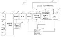
- FIG. 3is a simplified block diagram illustrating one exemplary embodiment of the present invention.
- the system 20includes a number of analog-digital converters (ADCs) 22 , a digital tuner 24 , a first data buffer 26 , an automatic gain control (AGC) 28 , a second data buffer 30 , and a demodulation engine 44 , all arranged in a sequential manner as shown in FIG. 3 .
- the demodulation engine 44further includes a timing recovery circuit 32 , a matched filter, equalizer and carrier recovery circuit 34 and a forward error correction (FEC) circuit 36 .
- ADCsanalog-digital converters
- ADCautomatic gain control
- FECforward error correction
- the first data buffer 26is controlled by a channel selector 38 ; and the time recovery circuit 32 , the matched filter, equalizer and carrier recovery circuit 34 and the FEC circuit 36 interact with both a channel switch control 40 and a channel status memory 42 .
- Each of the ADCs 22is a high-speed device that is capable of receiving and processing analog signals from a wideband channel.
- the wideband channelcovers at least one RF channel.
- the ADCs 22respectively convert analog signals from various RF channels to corresponding digital signals.
- Output from the ADCs 22is then relayed to the digital tuner 24 .
- the digital tuner 24is utilized to separate the RF channels in the digital domain.
- the separated signals from the RF channelsare then stored in the first data buffer 26 for subsequent processing.
- the channel selector 38is used to control how the corresponding data belonging to each RF channel is to be stored in the first data buffer 26 .
- Data from the first data buffer 26is then provided to the AGC 28 .
- the AGC 28is able to process data from multiple RF channels in a concurrent manner.
- the AGC 28is utilized to keep the signal strength of each individual channel at a relatively constant level. Keeping the signal strength of the RF channel at a relatively constant level ensures the proper functioning of a timing recovery circuit and an equalizer. It should be understood that a person of ordinary skill in the art should know of various ways and/or methods to implement the functions provided by the AGC 28 .
- Output from the AGC 28is then provided to the second data buffer 30 where it is stored for subsequent processing.
- the channel switch control 40is used to select the corresponding data belonging to the RF channel that is to be processed from the second data buffer 30 .
- the demodulation engine 44includes the timing recovery circuit 32 , the matched filter, equalizer and carrier recovery circuit 34 and the FEC circuit 36 .
- the timing recovery circuit 32is used to identify the optimal sampling time and restore signal values at the optimal sampling time.
- the matched filter, equalizer and carrier recovery circuit 34is utilized to remove channel echoes, minimize inter-symbol-interference, and compensate residual carrier frequency and phase shift.
- the FEC circuit 36is employed to extract coded data bit and correct transmission error.
- the system 20has three operating modes, namely, a channel switching mode, a data processing mode, and a waiting mode.
- the demodulation engine 44recovers a predetermined number of symbols from the current channel data corresponding to a particular channel.
- a person of ordinary skill in the artwill appreciate how to derive the predetermined number of symbols.
- the demodulation engine 44pauses for further processing instructions. Subsequent processing instructions may direct the demodulation engine 44 to engage in any one of the three operating modes. For example, the demodulation engine 44 may be directed to continue the data processing mode; alternatively, the demodulation engine may be switched into the channel switching mode or the waiting mode.
- the demodulation engine 44switches current channel data with selected data from another channel for processing. In other words, data from a new channel is loaded into the demodulation engine 44 for processing. More specifically, status and history information relating to the current channel is stored into the channel status memory 42 and current channel data is stored into the second data buffer 30 ; and status and history information relating to the next channel to be processed is retrieved from the channel status memory 42 and the corresponding channel data that is to be operated on is extracted from the second data buffer 30 and loaded into the demodulation engine 44 for processing.
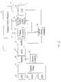
- FIG. 4illustrates one exemplary architecture used to provide optimized channel switching by the system 20 .
- a number of registers 46 and a number of buffers 48are positioned between the demodulation engine 44 and the channel status memory 42 .
- the registers 46are used to hold and supply status and history information relating to the current channel that is being processed by the demodulation engine 44 .
- the buffers 48are used to hold status and history information relating to the next channel that is to be processed.
- the status and history information relating to the next channel to be processedis preloaded into the buffers 48 from the channel status memory 42 .
- the corresponding status and history informationis put back into the channel status memory 42 and the status and history information corresponding to a new piece of data belonging to the next channel to be processed is preloaded into a buffer 48 from the channel status memory 42 .
- the demodulation engine 44enters the channel switching mode, information in the preloaded buffers 48 can be quickly transferred to the registers 46 for use when the demodulation engine 44 enters back into the data processing mode.
- the channel switching mode once initiatedcan be completed within fewer number of clock cycles.
- the reduction of channel switching timeallows the demodulation engine 44 to operate more efficiently, i.e., it allows the demodulation engine 44 to spend more time in the data processing mode thereby processing more data. As a result, more channels can be processed or higher throughput can be achieved.
- the demodulation engine 44In the waiting mode, the demodulation engine 44 remains idle for a certain period of time or number of clock cycles. This period of time or number of clock cycles can be either fixed or variable, depending on the design of a particular application.
- the demodulation engine 44may enter into the waiting mode when there is a gap between the data processing mode and the channel switching mode.
- the demodulation engine 44When in the waiting mode, the demodulation engine 44 is designed to have a power saving feature to reduce consumption of power.
- FIG. 5is a simplified timing diagram illustrating processing and switching of the channels by the demodulation engine 44 .
- the first and second data buffers 26 and 30there are two data buffers in the data path, namely, the first and second data buffers 26 and 30 .
- the first data buffer 26is located between the digital tuner 24 and the AGC 28
- the second data buffer 30is located between the AGC 28 and the timing recovery circuit 32 .
- the demodulation engine 44is shared amongst different RF channels. Referring to FIG. 5 , respective data from various channels are switched and processed by the system 20 .
- the timing recovery circuit 32when the timing recovery circuit 32 is processing data from Channel A, respective channel data belonging to Channel B and Channel C are stored in the second data buffer 30 and corresponding channel status and history information is also stored in the channel status memory 42 .
- the demodulation engine 44pauses for further processing instructions. The next processing instructions indicate that the demodulation engine 44 is to go into the waiting mode. Subsequently, at t 2 , the demodulation engine 44 is directed to enter the channel switching mode. Under the channel switching mode, the channel switch control 40 sends a command to switch the current channel to Channel B.
- channel data from Channel Ais stored into the second data buffer 30 and status and history information relating to Channel A is stored into the channel status memory 42 .
- the demodulation engine 44retrieves the corresponding channel data and status and history information relating to Channel B from the second data buffer 30 and the channel status memory 42 respectively.
- the channel switching timecan be optimized or reduced by the system 20 , if desired. This is accomplished by preloading status and history information relating to the next channel to be processed which, in this case, is Channel B during the data processing mode when data from Channel A is being processed. This allows the channel switching mode to be completed in fewer number of clock cycles.
- the demodulation engine 44enters into the data processing mode and begins to process the channel data belonging to Channel B. Similarly, at t 4 , the demodulation engine 44 enters into the channel switching mode again, this time, swapping channel data from Channel B to Channel C. Similarly, the channel switching time can be reduced by preloading status and history information relating to Channel C. At t 5 , the demodulation engine 44 resumes the data processing mode and begins to process channel data belonging to Channel C.
- the system 20includes a fully parallel low pass FIR filter.
- FIG. 6illustrates an exemplary embodiment of the fully parallel low pass FIR filter according to the present invention. As shown in FIG. 6 , this exemplary FIR filter is capable of handling five (5) channels in a concurrent manner with each channel having a 10-bit data stream. The identical data streams 50 a - e are generated based on an input data stream from a single channel. Identical data streams 50 a - e are provided to a number of multipliers 52 a - e in parallel.
- each multiplier 52 a - evaries depending on its corresponding coefficient.
- the size of multiplier 52 ais 10 ⁇ 10 (based on the 10-bit data stream and the 10-bit coefficient) and the size of multiplier 52 c is 10 ⁇ 4 (based on the 10-bit data stream and the 4-bit coefficient).
- the respective results from the multipliers 52 a - eare then added together by a number of adders 54 a - e to generate the output data.
- the fully parallel low pass FIR filter of the present inventioncan be deployed in various components of the system 20 .
- this filtercan be used in the digital tuner 24 and various components of the demodulation engine 44 including the timing recovery circuit 32 , the matched filter, equalizer and carrier recovery circuit 34 and the FEC circuit 36 .
- the timing recovery circuit 32the matched filter, equalizer and carrier recovery circuit 34 and the FEC circuit 36 .
- the present invention as described hereincan be implemented in various ways and/or manner.
- the system 20can be implemented using control logic in the form of software or hardware or a combination of both.
- a person of ordinary skill in the artwill know of other ways and/or methods to implement the present invention.
- the present inventioncan be deployed in various applications.
- the present inventioncan be incorporated in an integrated circuit chip within a communication system.
- a person of ordinary skill in the artwill know of other ways and/or applications in which to deploy the present invention.
Landscapes
- Engineering & Computer Science (AREA)
- Computer Networks & Wireless Communication (AREA)
- Signal Processing (AREA)
- Circuits Of Receivers In General (AREA)
Abstract
Description
Claims (39)
Priority Applications (1)
| Application Number | Priority Date | Filing Date | Title |
|---|---|---|---|
| US10/335,209US7388932B1 (en) | 2002-12-30 | 2002-12-30 | Fully parallel multi-channel demodulator |
Applications Claiming Priority (1)
| Application Number | Priority Date | Filing Date | Title |
|---|---|---|---|
| US10/335,209US7388932B1 (en) | 2002-12-30 | 2002-12-30 | Fully parallel multi-channel demodulator |
Publications (1)
| Publication Number | Publication Date |
|---|---|
| US7388932B1true US7388932B1 (en) | 2008-06-17 |
Family
ID=39510463
Family Applications (1)
| Application Number | Title | Priority Date | Filing Date |
|---|---|---|---|
| US10/335,209Expired - LifetimeUS7388932B1 (en) | 2002-12-30 | 2002-12-30 | Fully parallel multi-channel demodulator |
Country Status (1)
| Country | Link |
|---|---|
| US (1) | US7388932B1 (en) |
Cited By (7)
| Publication number | Priority date | Publication date | Assignee | Title |
|---|---|---|---|---|
| US20090033529A1 (en)* | 2007-07-16 | 2009-02-05 | Raz Gil M | System and method of multi-channel signal calibration |
| US7609192B1 (en)* | 2005-06-20 | 2009-10-27 | The Math Works, Inc. | Control of analog to digital conversion for analog I/O boards |
| US20100318689A1 (en)* | 2009-06-15 | 2010-12-16 | Thomson Licensing | Device for real-time streaming of two or more streams in parallel to a solid state memory device array |
| US9578469B2 (en) | 2014-10-02 | 2017-02-21 | Motorola Solutions, Inc. | Method and system for direct mode communication within a talkgroup |
| CN107070834A (en)* | 2017-02-09 | 2017-08-18 | 武汉米风通信技术有限公司 | Multiple channel demodulation method based on multichannel communication reception system |
| CN107453799A (en)* | 2017-06-30 | 2017-12-08 | 上海卫星工程研究所 | Satellite high data rate Ground Processing System and its method of testing |
| US11411950B2 (en)* | 2020-04-28 | 2022-08-09 | Bank Of America Corporation | Electronic system for integration of communication channels and active cross-channel communication transmission |
Citations (12)
| Publication number | Priority date | Publication date | Assignee | Title |
|---|---|---|---|---|
| WO1995012261A1 (en) | 1993-10-29 | 1995-05-04 | Airnet Communications Corp. | Wideband fft channelizer |
| WO1996034480A1 (en) | 1995-04-28 | 1996-10-31 | Qualcomm Incorporated | Method and apparatus for providing variable rate data in a communications system using statistical multiplexing |
| US6038435A (en)* | 1997-12-24 | 2000-03-14 | Nortel Networks Corporation | Variable step-size AGC |
| US6061406A (en)* | 1998-02-23 | 2000-05-09 | Motorola, Inc. | Multichannel time shared demodulator and method |
| US6122295A (en)* | 1995-06-08 | 2000-09-19 | Canon Kabushiki Kaisha | Multi-channel communication |
| JP2001069020A (en) | 1999-08-30 | 2001-03-16 | Matsushita Electric Ind Co Ltd | Digital broadcast receiver |
| US6205133B1 (en)* | 1996-11-25 | 2001-03-20 | Ericsson Inc. | Flexible wideband architecture for use in radio communications systems |
| US20010030940A1 (en)* | 1998-06-10 | 2001-10-18 | Richard Hellberg | Method and apparatus for digital channelisation and de-channelisation |
| US6466591B1 (en)* | 2000-12-30 | 2002-10-15 | Redback Networks Inc. | Method and apparatus for processing of multiple protocols within data and control channels in data transmission signals |
| US20030131191A1 (en) | 2001-11-26 | 2003-07-10 | Broadlogic Network Technologies, Inc. | Multi-stream access scheme for high speed access and recording using a hard disk drive |
| US6704372B2 (en)* | 2001-09-18 | 2004-03-09 | Broadlogic Network Technologies Inc. | Digital implementation of multi-channel demodulators |
| US6791995B1 (en)* | 2002-06-13 | 2004-09-14 | Terayon Communications Systems, Inc. | Multichannel, multimode DOCSIS headend receiver |
- 2002
- 2002-12-30USUS10/335,209patent/US7388932B1/ennot_activeExpired - Lifetime
Patent Citations (15)
| Publication number | Priority date | Publication date | Assignee | Title |
|---|---|---|---|---|
| WO1995012261A1 (en) | 1993-10-29 | 1995-05-04 | Airnet Communications Corp. | Wideband fft channelizer |
| JPH09507618A (en) | 1993-10-29 | 1997-07-29 | エアーネット・コミュニケーションズ・コーポレイション | Wideband channelizer |
| WO1996034480A1 (en) | 1995-04-28 | 1996-10-31 | Qualcomm Incorporated | Method and apparatus for providing variable rate data in a communications system using statistical multiplexing |
| US6005855A (en) | 1995-04-28 | 1999-12-21 | Qualcomm Incorporated | Method and apparatus for providing variable rate data in a communications system using statistical multiplexing |
| JP2003324776A (en) | 1995-04-28 | 2003-11-14 | Qualcomm Inc | Method and apparatus for providing variable rate data in communications system using statistical multiplexing |
| US6122295A (en)* | 1995-06-08 | 2000-09-19 | Canon Kabushiki Kaisha | Multi-channel communication |
| US6205133B1 (en)* | 1996-11-25 | 2001-03-20 | Ericsson Inc. | Flexible wideband architecture for use in radio communications systems |
| US6038435A (en)* | 1997-12-24 | 2000-03-14 | Nortel Networks Corporation | Variable step-size AGC |
| US6061406A (en)* | 1998-02-23 | 2000-05-09 | Motorola, Inc. | Multichannel time shared demodulator and method |
| US20010030940A1 (en)* | 1998-06-10 | 2001-10-18 | Richard Hellberg | Method and apparatus for digital channelisation and de-channelisation |
| JP2001069020A (en) | 1999-08-30 | 2001-03-16 | Matsushita Electric Ind Co Ltd | Digital broadcast receiver |
| US6466591B1 (en)* | 2000-12-30 | 2002-10-15 | Redback Networks Inc. | Method and apparatus for processing of multiple protocols within data and control channels in data transmission signals |
| US6704372B2 (en)* | 2001-09-18 | 2004-03-09 | Broadlogic Network Technologies Inc. | Digital implementation of multi-channel demodulators |
| US20030131191A1 (en) | 2001-11-26 | 2003-07-10 | Broadlogic Network Technologies, Inc. | Multi-stream access scheme for high speed access and recording using a hard disk drive |
| US6791995B1 (en)* | 2002-06-13 | 2004-09-14 | Terayon Communications Systems, Inc. | Multichannel, multimode DOCSIS headend receiver |
Non-Patent Citations (1)
| Title |
|---|
| English translation of Notice of Reasons for Rejection of Dec. 28, 2007 for Japanese application 2004-563171. |
Cited By (11)
| Publication number | Priority date | Publication date | Assignee | Title |
|---|---|---|---|---|
| US7609192B1 (en)* | 2005-06-20 | 2009-10-27 | The Math Works, Inc. | Control of analog to digital conversion for analog I/O boards |
| US20090033529A1 (en)* | 2007-07-16 | 2009-02-05 | Raz Gil M | System and method of multi-channel signal calibration |
| US7796068B2 (en)* | 2007-07-16 | 2010-09-14 | Gmr Research & Technology, Inc. | System and method of multi-channel signal calibration |
| US20100318689A1 (en)* | 2009-06-15 | 2010-12-16 | Thomson Licensing | Device for real-time streaming of two or more streams in parallel to a solid state memory device array |
| US8417846B2 (en)* | 2009-06-15 | 2013-04-09 | Thomson Licensing | Device for real-time streaming of two or more streams in parallel to a solid state memory device array |
| US9578469B2 (en) | 2014-10-02 | 2017-02-21 | Motorola Solutions, Inc. | Method and system for direct mode communication within a talkgroup |
| CN107070834A (en)* | 2017-02-09 | 2017-08-18 | 武汉米风通信技术有限公司 | Multiple channel demodulation method based on multichannel communication reception system |
| CN107070834B (en)* | 2017-02-09 | 2020-04-17 | 成都米风感知科技有限公司 | Multichannel demodulation method based on multichannel communication receiving system |
| CN107453799A (en)* | 2017-06-30 | 2017-12-08 | 上海卫星工程研究所 | Satellite high data rate Ground Processing System and its method of testing |
| CN107453799B (en)* | 2017-06-30 | 2020-08-25 | 上海卫星工程研究所 | Satellite high-speed data ground processing system and test method thereof |
| US11411950B2 (en)* | 2020-04-28 | 2022-08-09 | Bank Of America Corporation | Electronic system for integration of communication channels and active cross-channel communication transmission |
Similar Documents
| Publication | Publication Date | Title |
|---|---|---|
| US7236118B2 (en) | Multiple input analog-to-digital conversion apparatus and radio receiver using the same | |
| US20030056221A1 (en) | Digital implementation of multi-channel demodulators | |
| US5732337A (en) | Reconfigurable mixer-filter-decimator | |
| US7388932B1 (en) | Fully parallel multi-channel demodulator | |
| US6023717A (en) | Method and apparatus for polyphase digital filtering in a mobile telephone | |
| US20020003494A1 (en) | GPS receiver | |
| US6246444B1 (en) | Digital and analog TV common-use receiver having single ghost canceler and ghost cancellation method | |
| US7592942B2 (en) | Circuit and method for A/D conversion processing and demodulation device | |
| EP1579648B1 (en) | A fully parallel multi-channel demodulator | |
| JPH06104949A (en) | Fir filter | |
| KR20030047477A (en) | Device and method for cancelling narrow-band interference in wireless communication systems | |
| US7343140B2 (en) | Tuner | |
| US5263018A (en) | Apparatus for time division multiplexed processing of plural QAM signals | |
| JP5005622B2 (en) | Receiving device, tuner, and television receiver | |
| EP0583890A2 (en) | Apparatus for time division multiplexed processing of frequency division multiplexed signals | |
| US5432813A (en) | Parallel processing based digital matched filter and error detector for a digital demodulator | |
| US7196739B2 (en) | Multi-channel tuner apparatus | |
| US20060189291A1 (en) | Receiver and method for concurrent receiving of multiple channels | |
| KR20010089746A (en) | System and methods for multimode operation of a digital filter with shared resources | |
| US6999499B1 (en) | Demodulation apparatus of a base station in a CDMA mobile communication system | |
| US20060190967A1 (en) | Multi-channel satellite signal receiving apparatus |
Legal Events
| Date | Code | Title | Description |
|---|---|---|---|
| AS | Assignment | Owner name:BROADLOGIC NETWORK TECHNOLOGIES INC., CALIFORNIA Free format text:ASSIGNMENT OF ASSIGNORS INTEREST;ASSIGNORS:ZHANG, WEIMIN;RADIONOV, VLADIMIR;STENERSON, ROGER;AND OTHERS;REEL/FRAME:013958/0401 Effective date:20030404 | |
| STCF | Information on status: patent grant | Free format text:PATENTED CASE | |
| FPAY | Fee payment | Year of fee payment:4 | |
| AS | Assignment | Owner name:BROADCOM CORPORATION, CALIFORNIA Free format text:ASSIGNMENT OF ASSIGNORS INTEREST;ASSIGNOR:BROADLOGIC NETWORK TECHNOLOGIES, INC.;REEL/FRAME:030704/0725 Effective date:20130627 | |
| FEPP | Fee payment procedure | Free format text:PAT HOLDER NO LONGER CLAIMS SMALL ENTITY STATUS, ENTITY STATUS SET TO UNDISCOUNTED (ORIGINAL EVENT CODE: STOL); ENTITY STATUS OF PATENT OWNER: LARGE ENTITY | |
| FPAY | Fee payment | Year of fee payment:8 | |
| AS | Assignment | Owner name:BANK OF AMERICA, N.A., AS COLLATERAL AGENT, NORTH CAROLINA Free format text:PATENT SECURITY AGREEMENT;ASSIGNOR:BROADCOM CORPORATION;REEL/FRAME:037806/0001 Effective date:20160201 Owner name:BANK OF AMERICA, N.A., AS COLLATERAL AGENT, NORTH Free format text:PATENT SECURITY AGREEMENT;ASSIGNOR:BROADCOM CORPORATION;REEL/FRAME:037806/0001 Effective date:20160201 | |
| AS | Assignment | Owner name:AVAGO TECHNOLOGIES GENERAL IP (SINGAPORE) PTE. LTD., SINGAPORE Free format text:ASSIGNMENT OF ASSIGNORS INTEREST;ASSIGNOR:BROADCOM CORPORATION;REEL/FRAME:041706/0001 Effective date:20170120 Owner name:AVAGO TECHNOLOGIES GENERAL IP (SINGAPORE) PTE. LTD Free format text:ASSIGNMENT OF ASSIGNORS INTEREST;ASSIGNOR:BROADCOM CORPORATION;REEL/FRAME:041706/0001 Effective date:20170120 | |
| AS | Assignment | Owner name:BROADCOM CORPORATION, CALIFORNIA Free format text:TERMINATION AND RELEASE OF SECURITY INTEREST IN PATENTS;ASSIGNOR:BANK OF AMERICA, N.A., AS COLLATERAL AGENT;REEL/FRAME:041712/0001 Effective date:20170119 | |
| AS | Assignment | Owner name:AVAGO TECHNOLOGIES INTERNATIONAL SALES PTE. LIMITE Free format text:MERGER;ASSIGNOR:AVAGO TECHNOLOGIES GENERAL IP (SINGAPORE) PTE. LTD.;REEL/FRAME:047195/0658 Effective date:20180509 | |
| AS | Assignment | Owner name:AVAGO TECHNOLOGIES INTERNATIONAL SALES PTE. LIMITE Free format text:CORRECTIVE ASSIGNMENT TO CORRECT THE EFFECTIVE DATE OF MERGER PREVIOUSLY RECORDED ON REEL 047195 FRAME 0658. ASSIGNOR(S) HEREBY CONFIRMS THE THE EFFECTIVE DATE IS 09/05/2018;ASSIGNOR:AVAGO TECHNOLOGIES GENERAL IP (SINGAPORE) PTE. LTD.;REEL/FRAME:047357/0302 Effective date:20180905 | |
| AS | Assignment | Owner name:AVAGO TECHNOLOGIES INTERNATIONAL SALES PTE. LIMITE Free format text:CORRECTIVE ASSIGNMENT TO CORRECT THE ERROR IN RECORDING THE MERGER PREVIOUSLY RECORDED AT REEL: 047357 FRAME: 0302. ASSIGNOR(S) HEREBY CONFIRMS THE ASSIGNMENT;ASSIGNOR:AVAGO TECHNOLOGIES GENERAL IP (SINGAPORE) PTE. LTD.;REEL/FRAME:048674/0834 Effective date:20180905 | |
| MAFP | Maintenance fee payment | Free format text:PAYMENT OF MAINTENANCE FEE, 12TH YEAR, LARGE ENTITY (ORIGINAL EVENT CODE: M1553); ENTITY STATUS OF PATENT OWNER: LARGE ENTITY Year of fee payment:12 |