US7388450B2 - Packaged electronic components for producing a sub-harmonic frequency signal at millimetric frequencies - Google Patents
Packaged electronic components for producing a sub-harmonic frequency signal at millimetric frequenciesDownload PDFInfo
- Publication number
- US7388450B2 US7388450B2US10/534,251US53425105AUS7388450B2US 7388450 B2US7388450 B2US 7388450B2US 53425105 AUS53425105 AUS 53425105AUS 7388450 B2US7388450 B2US 7388450B2
- Authority
- US
- United States
- Prior art keywords
- free end
- component
- chips
- frequency
- line
- Prior art date
- Legal status (The legal status is an assumption and is not a legal conclusion. Google has not performed a legal analysis and makes no representation as to the accuracy of the status listed.)
- Expired - Lifetime
Links
- 230000007704transitionEffects0.000claimsabstractdescription27
- 230000008878couplingEffects0.000claimsabstractdescription22
- 238000010168coupling processMethods0.000claimsabstractdescription22
- 238000005859coupling reactionMethods0.000claimsabstractdescription22
- 239000000758substrateSubstances0.000claimsdescription30
- 239000000919ceramicSubstances0.000claimsdescription18
- 230000005540biological transmissionEffects0.000claimsdescription9
- 230000008859changeEffects0.000claimsdescription5
- 230000008054signal transmissionEffects0.000claimsdescription2
- 238000001465metallisationMethods0.000description12
- XUIMIQQOPSSXEZ-UHFFFAOYSA-NSiliconChemical compound[Si]XUIMIQQOPSSXEZ-UHFFFAOYSA-N0.000description3
- 238000004891communicationMethods0.000description3
- 238000004519manufacturing processMethods0.000description3
- 229910052710siliconInorganic materials0.000description3
- 239000010703siliconSubstances0.000description3
- JBRZTFJDHDCESZ-UHFFFAOYSA-NAsGaChemical compound[As]#[Ga]JBRZTFJDHDCESZ-UHFFFAOYSA-N0.000description2
- 229910001218Gallium arsenideInorganic materials0.000description2
- 239000000463materialSubstances0.000description2
- 229910000577Silicon-germaniumInorganic materials0.000description1
- 230000005670electromagnetic radiationEffects0.000description1
- 238000005516engineering processMethods0.000description1
- 238000012986modificationMethods0.000description1
- 230000004048modificationEffects0.000description1
- 230000009467reductionEffects0.000description1
- 239000011347resinSubstances0.000description1
- 229920005989resinPolymers0.000description1
- 239000004065semiconductorSubstances0.000description1
- 238000006467substitution reactionMethods0.000description1
Images

Classifications
- H—ELECTRICITY
- H01—ELECTRIC ELEMENTS
- H01P—WAVEGUIDES; RESONATORS, LINES, OR OTHER DEVICES OF THE WAVEGUIDE TYPE
- H01P5/00—Coupling devices of the waveguide type
- H01P5/08—Coupling devices of the waveguide type for linking dissimilar lines or devices
- H—ELECTRICITY
- H01—ELECTRIC ELEMENTS
- H01P—WAVEGUIDES; RESONATORS, LINES, OR OTHER DEVICES OF THE WAVEGUIDE TYPE
- H01P5/00—Coupling devices of the waveguide type
- H01P5/08—Coupling devices of the waveguide type for linking dissimilar lines or devices
- H01P5/10—Coupling devices of the waveguide type for linking dissimilar lines or devices for coupling balanced lines or devices with unbalanced lines or devices
- H01P5/107—Hollow-waveguide/strip-line transitions
- H—ELECTRICITY
- H01—ELECTRIC ELEMENTS
- H01L—SEMICONDUCTOR DEVICES NOT COVERED BY CLASS H10
- H01L2224/00—Indexing scheme for arrangements for connecting or disconnecting semiconductor or solid-state bodies and methods related thereto as covered by H01L24/00
- H01L2224/01—Means for bonding being attached to, or being formed on, the surface to be connected, e.g. chip-to-package, die-attach, "first-level" interconnects; Manufacturing methods related thereto
- H01L2224/42—Wire connectors; Manufacturing methods related thereto
- H01L2224/47—Structure, shape, material or disposition of the wire connectors after the connecting process
- H01L2224/48—Structure, shape, material or disposition of the wire connectors after the connecting process of an individual wire connector
- H01L2224/4805—Shape
- H01L2224/4809—Loop shape
- H01L2224/48091—Arched
- H—ELECTRICITY
- H01—ELECTRIC ELEMENTS
- H01L—SEMICONDUCTOR DEVICES NOT COVERED BY CLASS H10
- H01L2224/00—Indexing scheme for arrangements for connecting or disconnecting semiconductor or solid-state bodies and methods related thereto as covered by H01L24/00
- H01L2224/01—Means for bonding being attached to, or being formed on, the surface to be connected, e.g. chip-to-package, die-attach, "first-level" interconnects; Manufacturing methods related thereto
- H01L2224/42—Wire connectors; Manufacturing methods related thereto
- H01L2224/47—Structure, shape, material or disposition of the wire connectors after the connecting process
- H01L2224/48—Structure, shape, material or disposition of the wire connectors after the connecting process of an individual wire connector
- H01L2224/481—Disposition
- H01L2224/48151—Connecting between a semiconductor or solid-state body and an item not being a semiconductor or solid-state body, e.g. chip-to-substrate, chip-to-passive
- H01L2224/48221—Connecting between a semiconductor or solid-state body and an item not being a semiconductor or solid-state body, e.g. chip-to-substrate, chip-to-passive the body and the item being stacked
- H01L2224/48225—Connecting between a semiconductor or solid-state body and an item not being a semiconductor or solid-state body, e.g. chip-to-substrate, chip-to-passive the body and the item being stacked the item being non-metallic, e.g. insulating substrate with or without metallisation
- H01L2224/48227—Connecting between a semiconductor or solid-state body and an item not being a semiconductor or solid-state body, e.g. chip-to-substrate, chip-to-passive the body and the item being stacked the item being non-metallic, e.g. insulating substrate with or without metallisation connecting the wire to a bond pad of the item
Definitions
- the inventionrelates to electronic circuits working at very high frequencies, greater than 45 GHz, also called “millimetric frequencies”.
- These electronic circuitsare used for radar type applications in which an electromagnetic wave is sent at a millimetric frequency and a wave reflected by an obstacle is received by an antenna, to extract from this wave, on the one hand, distance information and, on the other hand, relative speed information, between this obstacle and the source that sent the wave.
- the millimetric frequency circuitscan also be used for short distance and very high bit rate communication applications.
- the electronic processing of the millimetric frequency signalscomprises a low frequency processing part that can be implemented by silicon integrated circuits mounted on printed circuits.
- This partcan be produced by very commonly used and inexpensive technologies, with connections that are simple to produce between circuit elements on one and the same integrated circuit chip or between different integrated circuit chips.
- the processingalso comprises a very high frequency part (greater than 45 GHz), that can be implemented only by components and integrated circuits made of semiconductor materials other than silicon (gallium arsenide GaAs and its derivatives in particular, or even SiGe). These integrated circuits are called “microwave monolithic integrated circuits” or MMIC. This high-frequency part raises problems of production that are difficult and usually prove very expensive.
- MMIC integrated circuit chipsIn practice, for relatively complex functions, it is necessary to use a large number of MMIC integrated circuit chips, since the quantity of circuit elements that can be placed in one and the same chip is far more limited for the MMIC circuits than for the low frequency circuits made of silicon. Also, these chips are mounted on a substrate with interconnections that are difficult to produce given the very high working frequencies. The design of the interconnections is difficult, and the production cost is high because of the precision required in maintaining tight tolerances to ensure the transmission of the millimetric frequency signals. This becomes all the more true as the number of MMIC chips increases in the system. Also, the increase in complexity of the functions that are to be produced brings with it an increase in the number of chips.
- the object of the present inventionis to reduce the cost of the electronic systems operating at millimetric frequencies greater than 45 GHz (and preferably greater than 60 GHz) and including MMIC chips.
- This electronic componentis a component mounted in an individual package and intended to be connected to other components of an electronic system, for example on a printed circuit board with a number of components; this component comprises at least one integrated circuit chip MMIC working around a main millimetric frequency F greater than 45 GHz.
- the packagehas at least two ports for communicating electrical signals between the interior and the exterior of the package, the first port being a port with transition by electromagnetic coupling (i.e. without physical electrical contact) for the transmission of the main working frequency greater than 45 GHz, and the second port being a port with microstrip or coaxial type transition for the transmission of a working frequency F/N that is a subharmonic of the main frequency F.
- the subharmonic frequencyis preferably one of the following four frequencies: F/6 or F/4 or F/3 (or, in extreme cases, it could be F/2).
- the subharmonic frequencyis therefore 1/6 or 1/4 or 1/3 of 77 GHz.
- the packageis preferably provided with a conductive cover positioned at a distance from the first port that create, near this port, an electromagnetic short circuit at the main working frequency, this short circuit forming a wave reflector facilitating the contactless transmission of this frequency through the first port.
- the height of the conductive cover above the first portis preferably equal to a quarter of the wavelength of the main working frequency, to provide this short circuit and reflector role. This height can also be an odd multiple of a quarter of the wavelength.
- One or more of MMIC chips present in the packagewill preferably comprise means of multiplying in a ratio N to change from the subharmonic frequency to the main working frequency. It could also, in certain cases, include means of dividing frequencies in the ratio N.
- the componenttherefore has the specific feature that it includes a port with no physical contact, dedicated to the passage of signals at the main frequency, and a port with contact dedicated to the passage of signals at the subharmonic frequency.
- FIG. 1represents a millimetric package component according to the invention
- FIG. 2represents a component according to the invention associated with a radar antenna.
- a typical application in which the component according to the invention can be usedis a radar application, in which, on the one hand, a millimetric frequency greater than 45 GHz, in this example, a frequency of 77 GHz, is to be sent by a first antenna and, on the other hand, the electromagnetic wave reflected by an obstacle is to be received by several different antennas. It therefore concerns a multiple-beam radar. The presence of several receive antennas makes it possible to observe the presence of obstacles in a wider angular field and also to locate the detected obstacle with greater accuracy.
- millimetric packagescapable of working at frequencies greater than 45 GHz, and having external ports to allow for a link by contactless electromagnetic coupling at the working frequency, in this case 77 GHz, with transmit or receive antennas or with waveguides leading to these antennas.
- the transmission by electromagnetic coupling at these very high frequenciesis provided by the use of the free propagation properties of the electromagnetic signals inside the package and, above all, between the inside and the outside.
- This packagecomprises in particular a conductive cover (metallic or metallized cover) which encloses the propagation lines of the signals from the chip or to the chip.
- the conductive coveris located above the contactless external port, at a distance such that it forms (at the main working frequency for which the component is designed) an electromagnetic short circuit facilitating signal transmission in free propagation mode via this port.
- the ports at the working frequency F of more than 45 GHzare transitions by electromagnetic coupling in air (or in a gas or in a vacuum) and in particular conductive elements capable of radiating towards a waveguide placed in line with these elements, or capable of receiving an electromagnetic radiation at the output of a waveguide that they are placed in front of.
- the package enclosing the MMIC chipsincludes a non-conductive part in line with these conductive elements so as to allow the electromagnetic energy to pass between the waveguide and the conductive elements.
- the packagepreferably has, in addition to one or more external contactless ports capable of effective coupling at greater than 45 GHz, ports not capable of working effectively at a frequency greater than 45 GHz but designed to work at a subharmonic frequency of the working frequency. Also, the chips contained in these components then preferably include the necessary frequency multiplication means to change from the subharmonic frequency to the main frequency.
- the ports not capable of working at 77 GHz but capable of working above 10 GHz, even up to 25 GHz or a little above,are produced using microstrip lines or coaxial lines.
- the connection of the component with other components placed on the same substratewill be made easily because the frequencies carried are far lower than the millimetric working frequency.
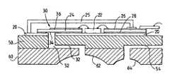
- FIG. 1is a cross-sectional representation of a component according to the invention. This example shows only one MMIC chip in the package of the component, but there can be two, or even, in exceptional cases, three.
- the packageis conductive, for example metallic or partially metallic; it preferably includes a metallic base 20 , serving as a substrate on which is directly mounted the rear face of the MMIC chip 22 , a double-sided ceramic substrate 24 providing the interconnections inside the package and towards the outside of the package, and a metallic or metallized cover 25 covering the base, to enclose, between the base and the cover, the chip or chips and the ceramic substrate. Since the MMIC chip 22 is welded directly onto the base, the ceramic substrate 24 includes an opening in which the chip is inserted.
- the ceramic substrate 24is preferably a substrate metallized on both sides: as shown in FIGS. 1 and 2 , metallization 26 on the front side forms the transmission lines, and metallization 28 on the rear side forms a ground plane.
- the dimensions of the various dielectric and conductive partsare such that the component operates correctly at the working frequency concerned (77 GHz).
- the metallizations 26 and 28are used, to create the interconnections between chips and, to create the external ports of the package, both the ports capable of working at 77 GHz and the ports designed to transmit a frequency that is a subharmonic at 77 GHz.
- the port 30 capable of transmitting the 77 GHz frequencycomprises a transition by contactless electromagnetic coupling enabling the signal at the frequency of 77 GHz to pass without contact from a waveguide to the chip or vice versa.
- This transition by electromagnetic couplingis preferably via an opening 32 in the package, and more specifically in the metallic base 20 .
- This opening 32communicates with a waveguide not shown in FIG. 1 .
- This openingis physically, but not electromagnetically, closed by the ceramic substrate 24 . It is in line with a demetallized area 34 provided in the metallization 28 of the rear side of the ceramic substrate.
- the end 36 of the microstrip lineterminates exactly in line with the center of the opening 32 of the base 20 .
- This end 36together with the demetallized area 34 which is surrounded by the metallization 28 forming a ground plane, forms a radiating element, therefore an antenna, communicating, for example, with a waveguide placed in front of the opening 32 , directly coupling the waveguide with the microstrip line by electromagnetic means.
- the conductive surface of the coveris located at a distance suited to the wavelength of the main working frequency of the signals transmitted by this line, this distance being such that the cover forms an electromagnetic short circuit and therefore a reflector for the antenna radiated by the end 36 of the microstrip line.
- the height H of the cover above the metallization of the ceramic substrate 24is equal to a quarter of the wavelength corresponding to this frequency or very close to this value. It can also be an odd multiple of a quarter of the wavelength.
- a wired link 38is provided between the chip and the line.
- the resulting couplingoperates at 77 GHz provided that the dimensions of the metallized and non-metallized areas, the thickness of the ceramic substrate and the width of the opening in the ceramic substrate are chosen correctly, suited to the wavelength corresponding to the main frequency of 77 GHz.
- the waveguideis connected to an antenna receiving (or transmitting) the reflected radar wave, and the end 36 of the microstrip line acts as an element for receiving an electromagnetic wave entering into the package.
- the other port shown in FIG. 1is a direct port 40 by microstrip line, not allowing a communication at 77 GHz but allowing a communication at a subharmonic frequency which is preferably F/6 but which can also be F/4 or F/3, or even F/2 in certain cases.
- the microstrip line corresponding to this portis formed in the top metallization 26 of the metallized ceramic substrate 24 .
- the bottom metallization 28serves as a ground plane.
- the linepasses from the inside to the outside of the package via a local interruption of the conductive cover 25 , by insulating the microstrip line from the cover, for example by an insulating washer 42 interposed between the line and the edge of the cover, or via a notch in the cover.
- the MMIC chipOn the side of this subharmonic frequency port 40 , the MMIC chip is also linked to the microstrip line by a wired link 44 .
- the componentcan be connected externally by the port 40 with another similar component mounted on the same hybrid substrate, or with a different component mounted on the same hybrid substrate or mounted on a conventional printed circuit.
- This connectioncan be made directly from the top metallization surface 26 which extends outside the package; for example, a wire can be soldered to this top surface; or it can even be via a lead 46 soldered to this external part of the metallization 26 and then forming an integral part of the component.
- FIG. 2represents the use of the component of FIG. 1 in a radar electronic system.
- the assemblybase 20 , chip 22 , cover 25 .
- the base 20is mounted directly in contact with a metallic plate 50 which is a waveguide plate: in this plate, a waveguide 52 is formed, the output end of which is just in line with the opening 32 of the base 20 , therefore in line with the conductive end 36 which provides an electromagnetic coupling between the waveguide and the package.
- the other end of the waveguideis in line with the transmission center of a parabolic radar receive antenna 62 machined in a metallic plate 60 placed against the waveguide plate 50 .
- the waveguide plate 50can include a number of waveguides, for example a second guide 54 leading to a second antenna 64 machined in the same antenna plate 60 ; this guide directs the electromagnetic wave received from the second antenna to a second millimetric packaged component, not shown, similar to the component of FIG. 1 and mounted like the latter on the plate 50 forming a substrate common to a number of components according to the invention.
- the ceramic substrate 24was fixed on a metallic base. It is possible to envisage no metallic base, the package being formed by the ceramic substrate, metallized on both sides, and the metallic cover. In this case, the port 30 with transition by electromagnetic coupling is produced in exactly the same way; the demetallized area 34 provided in the rear metallization 28 takes the place of the opening 32 which does not exist since the base does not exist. The waveguide is exactly in line with this demetallization.
- the microstrip linea free end of which is used as a contactless electromagnetic transition
- the MMIC chipthe same as or other than the chip 22
- the MMIC chipthus used as an electromagnetic transition is fixed on a metallic base of the package, a part of the chip extending in line with an opening provided in the base, opening which is itself in line with a waveguide.
- the free end of the microstrip line carried by the MMIC chipis then in line with the opening in the base to form a contactless electromagnetic transition through this opening.
- transition by electromagnetic couplingwhich uses the cover of the package as a reflector to produce the transition.
- other types of transition by couplingfor example non-reflector transitions, using the geometry of the different elements of the package to facilitate the electromagnetic coupling.
- a reflectoris not then necessary and this embodiment would be suited in particular to cases in which the cover of the package was of plastic material.
- Components according to the inventioncan be used to produce complete electronic systems on inexpensive printed circuit substrates (resin-based substrates) combining low-frequency components (integrated circuit chips or other components operating at low frequency), and components operating up to approximately 25 GHz. These components are linked to millimetric packaged components according to the invention by microstrip connections, and the millimetric packaged components are connected to antennas by transitions with contactless electromagnetic coupling and by waveguides.
Landscapes
- Waveguide Aerials (AREA)
- Radar Systems Or Details Thereof (AREA)
- Transceivers (AREA)
- Waveguide Connection Structure (AREA)
- Variable-Direction Aerials And Aerial Arrays (AREA)
Abstract
Description
The present Application is based on International Application No. PCT/EP2003/050846, filed on Nov. 18, 2003, which in turn corresponds to FR 02/14684 filed on Nov. 22, 2002, and priority is hereby claimed under 35 USC § 119 based on these applications. Each of these applications are hereby incorporated by reference in their entirety into the present application.
The invention relates to electronic circuits working at very high frequencies, greater than 45 GHz, also called “millimetric frequencies”.
These electronic circuits are used for radar type applications in which an electromagnetic wave is sent at a millimetric frequency and a wave reflected by an obstacle is received by an antenna, to extract from this wave, on the one hand, distance information and, on the other hand, relative speed information, between this obstacle and the source that sent the wave.
The millimetric frequency circuits can also be used for short distance and very high bit rate communication applications.
Whatever the application, the electronic processing of the millimetric frequency signals comprises a low frequency processing part that can be implemented by silicon integrated circuits mounted on printed circuits. This part can be produced by very commonly used and inexpensive technologies, with connections that are simple to produce between circuit elements on one and the same integrated circuit chip or between different integrated circuit chips. The processing also comprises a very high frequency part (greater than 45 GHz), that can be implemented only by components and integrated circuits made of semiconductor materials other than silicon (gallium arsenide GaAs and its derivatives in particular, or even SiGe). These integrated circuits are called “microwave monolithic integrated circuits” or MMIC. This high-frequency part raises problems of production that are difficult and usually prove very expensive.
In practice, for relatively complex functions, it is necessary to use a large number of MMIC integrated circuit chips, since the quantity of circuit elements that can be placed in one and the same chip is far more limited for the MMIC circuits than for the low frequency circuits made of silicon. Also, these chips are mounted on a substrate with interconnections that are difficult to produce given the very high working frequencies. The design of the interconnections is difficult, and the production cost is high because of the precision required in maintaining tight tolerances to ensure the transmission of the millimetric frequency signals. This becomes all the more true as the number of MMIC chips increases in the system. Also, the increase in complexity of the functions that are to be produced brings with it an increase in the number of chips.
Mounting the chips on a hybrid substrate (normally mounting with wiring to link the chips to the hybrid substrate) is itself very expensive when the number of chips is high.
The object of the present invention is to reduce the cost of the electronic systems operating at millimetric frequencies greater than 45 GHz (and preferably greater than 60 GHz) and including MMIC chips.
To achieve this cost reduction, the invention proposes to use a new type of component to produce the system. This electronic component is a component mounted in an individual package and intended to be connected to other components of an electronic system, for example on a printed circuit board with a number of components; this component comprises at least one integrated circuit chip MMIC working around a main millimetric frequency F greater than 45 GHz. The package has at least two ports for communicating electrical signals between the interior and the exterior of the package, the first port being a port with transition by electromagnetic coupling (i.e. without physical electrical contact) for the transmission of the main working frequency greater than 45 GHz, and the second port being a port with microstrip or coaxial type transition for the transmission of a working frequency F/N that is a subharmonic of the main frequency F.
The subharmonic frequency is preferably one of the following four frequencies: F/6 or F/4 or F/3 (or, in extreme cases, it could be F/2).
For a working frequency at 77 GHz, the subharmonic frequency is therefore 1/6 or 1/4 or 1/3 of 77 GHz.
The package is preferably provided with a conductive cover positioned at a distance from the first port that create, near this port, an electromagnetic short circuit at the main working frequency, this short circuit forming a wave reflector facilitating the contactless transmission of this frequency through the first port.
The height of the conductive cover above the first port is preferably equal to a quarter of the wavelength of the main working frequency, to provide this short circuit and reflector role. This height can also be an odd multiple of a quarter of the wavelength.
One or more of MMIC chips present in the package will preferably comprise means of multiplying in a ratio N to change from the subharmonic frequency to the main working frequency. It could also, in certain cases, include means of dividing frequencies in the ratio N.
The component therefore has the specific feature that it includes a port with no physical contact, dedicated to the passage of signals at the main frequency, and a port with contact dedicated to the passage of signals at the subharmonic frequency.
Still other objects and advantages of the present invention will become readily apparent to those skilled in the art from the following detailed description, wherein the preferred embodiments of the invention are shown and described, simply by way of illustration of the best mode contemplated of carrying out the invention. As will be realized, the invention is capable of other and different embodiments, and its several details are capable of modifications in various obvious respects, all without departing from the invention. Accordingly, the drawings and description thereof are to be regarded as illustrative in nature, and not as restrictive.
Other features and advantages of the invention will become apparent from reading the detailed description that follows and which is given with reference to the appended drawings in which:
A typical application in which the component according to the invention can be used is a radar application, in which, on the one hand, a millimetric frequency greater than 45 GHz, in this example, a frequency of 77 GHz, is to be sent by a first antenna and, on the other hand, the electromagnetic wave reflected by an obstacle is to be received by several different antennas. It therefore concerns a multiple-beam radar. The presence of several receive antennas makes it possible to observe the presence of obstacles in a wider angular field and also to locate the detected obstacle with greater accuracy.
According to the invention, it is proposed to place the MMIC chips individually in sealed packages, called millimetric packages, capable of working at frequencies greater than 45 GHz, and having external ports to allow for a link by contactless electromagnetic coupling at the working frequency, in this case 77 GHz, with transmit or receive antennas or with waveguides leading to these antennas.
The transmission by electromagnetic coupling at these very high frequencies is provided by the use of the free propagation properties of the electromagnetic signals inside the package and, above all, between the inside and the outside. This package comprises in particular a conductive cover (metallic or metallized cover) which encloses the propagation lines of the signals from the chip or to the chip. The conductive cover is located above the contactless external port, at a distance such that it forms (at the main working frequency for which the component is designed) an electromagnetic short circuit facilitating signal transmission in free propagation mode via this port.
The ports at the working frequency F of more than 45 GHz are transitions by electromagnetic coupling in air (or in a gas or in a vacuum) and in particular conductive elements capable of radiating towards a waveguide placed in line with these elements, or capable of receiving an electromagnetic radiation at the output of a waveguide that they are placed in front of. The package enclosing the MMIC chips includes a non-conductive part in line with these conductive elements so as to allow the electromagnetic energy to pass between the waveguide and the conductive elements.
The package preferably has, in addition to one or more external contactless ports capable of effective coupling at greater than 45 GHz, ports not capable of working effectively at a frequency greater than 45 GHz but designed to work at a subharmonic frequency of the working frequency. Also, the chips contained in these components then preferably include the necessary frequency multiplication means to change from the subharmonic frequency to the main frequency.
The ports not capable of working at 77 GHz but capable of working above 10 GHz, even up to 25 GHz or a little above, are produced using microstrip lines or coaxial lines. The connection of the component with other components placed on the same substrate will be made easily because the frequencies carried are far lower than the millimetric working frequency.
The package is conductive, for example metallic or partially metallic; it preferably includes ametallic base 20, serving as a substrate on which is directly mounted the rear face of theMMIC chip 22, a double-sidedceramic substrate 24 providing the interconnections inside the package and towards the outside of the package, and a metallic or metallizedcover 25 covering the base, to enclose, between the base and the cover, the chip or chips and the ceramic substrate. Since theMMIC chip 22 is welded directly onto the base, theceramic substrate 24 includes an opening in which the chip is inserted. Theceramic substrate 24 is preferably a substrate metallized on both sides: as shown inFIGS. 1 and 2 ,metallization 26 on the front side forms the transmission lines, andmetallization 28 on the rear side forms a ground plane. The dimensions of the various dielectric and conductive parts are such that the component operates correctly at the working frequency concerned (77 GHz). Themetallizations
In the example ofFIG. 1 , theport 30 capable of transmitting the 77 GHz frequency comprises a transition by contactless electromagnetic coupling enabling the signal at the frequency of 77 GHz to pass without contact from a waveguide to the chip or vice versa.
This transition by electromagnetic coupling is preferably via anopening 32 in the package, and more specifically in themetallic base 20. This opening32 communicates with a waveguide not shown inFIG. 1 . This opening is physically, but not electromagnetically, closed by theceramic substrate 24. It is in line with ademetallized area 34 provided in themetallization 28 of the rear side of the ceramic substrate. On thefront metallization 26, forming a microstrip line from theMMIC chip 22 to theport 30, theend 36 of the microstrip line terminates exactly in line with the center of theopening 32 of thebase 20. Thisend 36, together with thedemetallized area 34 which is surrounded by themetallization 28 forming a ground plane, forms a radiating element, therefore an antenna, communicating, for example, with a waveguide placed in front of theopening 32, directly coupling the waveguide with the microstrip line by electromagnetic means. Above theend 36 of the microstrip line, the conductive surface of the cover is located at a distance suited to the wavelength of the main working frequency of the signals transmitted by this line, this distance being such that the cover forms an electromagnetic short circuit and therefore a reflector for the antenna radiated by theend 36 of the microstrip line. For example, the height H of the cover above the metallization of theceramic substrate 24, is equal to a quarter of the wavelength corresponding to this frequency or very close to this value. It can also be an odd multiple of a quarter of the wavelength.
At the other end of the microstrip line, a wired link38 is provided between the chip and the line. The resulting coupling operates at 77 GHz provided that the dimensions of the metallized and non-metallized areas, the thickness of the ceramic substrate and the width of the opening in the ceramic substrate are chosen correctly, suited to the wavelength corresponding to the main frequency of 77 GHz.
In the main application envisaged, the waveguide is connected to an antenna receiving (or transmitting) the reflected radar wave, and theend 36 of the microstrip line acts as an element for receiving an electromagnetic wave entering into the package.
The other port shown inFIG. 1 is adirect port 40 by microstrip line, not allowing a communication at 77 GHz but allowing a communication at a subharmonic frequency which is preferably F/6 but which can also be F/4 or F/3, or even F/2 in certain cases. The microstrip line corresponding to this port is formed in thetop metallization 26 of the metallizedceramic substrate 24. Thebottom metallization 28 serves as a ground plane. The line passes from the inside to the outside of the package via a local interruption of theconductive cover 25, by insulating the microstrip line from the cover, for example by an insulatingwasher 42 interposed between the line and the edge of the cover, or via a notch in the cover.
On the side of thissubharmonic frequency port 40, the MMIC chip is also linked to the microstrip line by awired link 44.
The component can be connected externally by theport 40 with another similar component mounted on the same hybrid substrate, or with a different component mounted on the same hybrid substrate or mounted on a conventional printed circuit. This connection can be made directly from thetop metallization surface 26 which extends outside the package; for example, a wire can be soldered to this top surface; or it can even be via alead 46 soldered to this external part of themetallization 26 and then forming an integral part of the component.
It will therefore be understood that in an electronic system using this component, a common substrate will have mounted on it not individual chips but components of the type that has just been described, so significantly simplifying the design and fabrication of the system.
The other end of the waveguide, the input end in this application, is in line with the transmission center of a parabolic radar receiveantenna 62 machined in ametallic plate 60 placed against thewaveguide plate 50. Thewaveguide plate 50 can include a number of waveguides, for example asecond guide 54 leading to asecond antenna 64 machined in thesame antenna plate 60; this guide directs the electromagnetic wave received from the second antenna to a second millimetric packaged component, not shown, similar to the component ofFIG. 1 and mounted like the latter on theplate 50 forming a substrate common to a number of components according to the invention.
In the embodiments ofFIGS. 1 and 2 , it was assumed that theceramic substrate 24 was fixed on a metallic base. It is possible to envisage no metallic base, the package being formed by the ceramic substrate, metallized on both sides, and the metallic cover. In this case, theport 30 with transition by electromagnetic coupling is produced in exactly the same way; thedemetallized area 34 provided in therear metallization 28 takes the place of theopening 32 which does not exist since the base does not exist. The waveguide is exactly in line with this demetallization.
In a different embodiment, it is possible to provide for the microstrip line, a free end of which is used as a contactless electromagnetic transition, to be carried by an MMIC chip (the same as or other than the chip22) instead of being carried by a ceramic substrate as is the case inFIGS. 1 and 2 . In this case, the MMIC chip thus used as an electromagnetic transition is fixed on a metallic base of the package, a part of the chip extending in line with an opening provided in the base, opening which is itself in line with a waveguide. The free end of the microstrip line carried by the MMIC chip is then in line with the opening in the base to form a contactless electromagnetic transition through this opening.
The description above proposes a transition by electromagnetic coupling which uses the cover of the package as a reflector to produce the transition. However, it is possible also to envisage other types of transition by coupling, for example non-reflector transitions, using the geometry of the different elements of the package to facilitate the electromagnetic coupling. For example, a transition that uses an electromagnetic coupling between a microstrip line on the top side of the substrate24 (or of the chip22) and a slot line (demetallization 34 in the form of a slot) on the bottom side. A reflector is not then necessary and this embodiment would be suited in particular to cases in which the cover of the package was of plastic material.
Components according to the invention can be used to produce complete electronic systems on inexpensive printed circuit substrates (resin-based substrates) combining low-frequency components (integrated circuit chips or other components operating at low frequency), and components operating up to approximately 25 GHz. These components are linked to millimetric packaged components according to the invention by microstrip connections, and the millimetric packaged components are connected to antennas by transitions with contactless electromagnetic coupling and by waveguides.
It will be readily seen by one of ordinary skill in the art that the present invention fulfills all of the objects set forth above. After reading the foregoing specification, one of ordinary skill will be able to affect various changes, substitutions of equivalents and various other aspects of the invention as broadly disclosed herein. It is therefore intended that the protection granted hereon be limited only by the definition contained in the appended claims and equivalents thereof.
Claims (17)
1. An electronic component mounted in an individual package and intended to be connected to other components of an electronic system, said electronic component comprising:
one or more integrated circuit chips working around a main millimetric frequency F greater than 45 GHz, wherein said package has at least two ports for communicating electrical signals between the interior and the exterior of said package, the first port being a port with transition by contactless electromagnetic coupling for the transmission of signals at the main frequency greater than 45 GHz, and the second port being a port with microstrip or coaxial type transition for the transmission of a main frequency F/N that is a subharmonic of the frequency F, where N is ≧2.
2. The component as claimed inclaim 1 , wherein the package is provided with a conductive cover positioned at a distance from the first port such that said conductive cover sets up, above this port, an electromagnetic short circuit at the main frequency, thus forming a wave reflector facilitating the transmission of said main frequency through the first port.
3. The component as claimed inclaim 2 , wherein the conductive cover is at a height above the port equal to a quarter of the wavelength, or an odd multiple of the quarter of the wavelength of the main frequency.
4. The component as claimed inclaim 3 , wherein one of the chips included in said package comprises means for multiplying frequency by a ratio N to change from the subharmonic frequency to the main frequency.
5. The component as claimed inclaim 3 , comprising a ceramic substrate, a first metallized side of which is etched to form a microstrip line having a free end and another side of which is also metallized to form a ground plane, the ground plane being interrupted facing the free end, to provide contactless electromagnetic coupling between the interior and the exterior of the package via the microstrip free end.
6. The component as claimed inclaim 3 wherein said one or more chips including one or more MMIC chips fixed on a base, said one of the chips MMIC including a microstrip line, having one free end in which used as the contactless electromagnetic transition, said one MMIC chip extending over an opening in the base so that the free end of the line is located in line with the opening, in order to form a contactless electromagnetic transition through the opening.
7. The component as claimed inclaim 2 , comprising a ceramic substrate, a first metallized side of which is etched to form a microstrip line having a free end and another side of which is also metallized to form a ground plane, the ground plane being interrupted facing the free end, to provide contactless electromagnetic coupling between the interior and the exterior of the package via the microstrip free end.
8. The component as claimed inclaim 2 , wherein said one or more chips including one or more MMIC chips fixed on a base, one of the chips MMIC including a microstrip line, having one free end which is used as the contactless electromagnetic transition, said one MMIC chip extending over an opening in the base so that the free end of the line is located in line with the opening, in order to form the contactless electromagnetic transition through the opening.
9. The component as claimed inclaim 2 , wherein one of the chips included in said package comprises means for multiplying frequency by a ratio N to change from the subharmonic frequency to the main frequency.
10. The component as claimed inclaim 1 , wherein said one or more chips comprising one or more MMIC chips fixed on a base, one of the chips MMIC including a microstrip line, having one free end which is used as the contactless electromagnetic transition, said one MMIC chip extending over an opening in the base so that the free end of the line is located in line with the opening, in order to form the contactless electromagnetic transition through the opening.
11. The component as claimed inclaim 1 , wherein one of the chips included in said package comprises means for multiplying frequency by a ratio N to change from the subharmonic frequency to the main frequency.
12. The component as claimed inclaim 11 , wherein said one or more chips including one or more MMIC chips fixed on a base, said one of the chips MMIC including a microstrip line, having one free end which is used as the contactless electromagnetic transition, said one MMIC chip extending over an opening in the base so that the free end of the line is located in line with the opening, in order to form the contactless electromagnetic transition through the opening.
13. The component as claimed inclaim 11 , comprising a ceramic substrate, a first metallized side of which is etched to form a microstrip line having a free end and another side of which is also metallized to form a ground plane, the ground plane being interrupted facing the free end, to provide contactless electromagnetic coupling between the interior and the exterior of the package via the microstrip free end.
14. The component as claimed inclaim 1 , comprising a ceramic substrate, a first metallized side of which is etched to form a microstrip line having a free end and another side of the ceramic subtrate is also metallized to form a ground plane, the ground plane being interrupted facing the free end, to provide the contactless electromagnetic coupling between the interior and the exterior of the package via the microstrip free end.
15. The component as claimed inclaim 14 , wherein a conductive cover is at a height above the free end of the microstrip line equal to a quarter of the wavelength, or an odd multiple of a quarter of the wavelength of the main frequency.
16. The component as claimed inclaim 15 , including a metallic base open facing the microstrip free end.
17. The component as claimed inclaim 14 , comprising a metallic base open facing the microstrip free end.
Applications Claiming Priority (3)
| Application Number | Priority Date | Filing Date | Title |
|---|---|---|---|
| FR0214684 | 2002-11-22 | ||
| FR0214684AFR2847723B1 (en) | 2002-11-22 | 2002-11-22 | ELECTRONIC HOUSING COMPONENT FOR MILLIMETER FREQUENCY APPLICATIONS |
| PCT/EP2003/050846WO2004049496A1 (en) | 2002-11-22 | 2003-11-18 | Packaged electronic component for applications at millimetric frequencies |
Publications (2)
| Publication Number | Publication Date |
|---|---|
| US20060097818A1 US20060097818A1 (en) | 2006-05-11 |
| US7388450B2true US7388450B2 (en) | 2008-06-17 |
Family
ID=32241535
Family Applications (1)
| Application Number | Title | Priority Date | Filing Date |
|---|---|---|---|
| US10/534,251Expired - LifetimeUS7388450B2 (en) | 2002-11-22 | 2003-11-18 | Packaged electronic components for producing a sub-harmonic frequency signal at millimetric frequencies |
Country Status (8)
| Country | Link |
|---|---|
| US (1) | US7388450B2 (en) |
| EP (1) | EP1563567A1 (en) |
| JP (1) | JP2006507740A (en) |
| KR (1) | KR20050059339A (en) |
| CN (1) | CN100517861C (en) |
| AU (1) | AU2003300245A1 (en) |
| FR (1) | FR2847723B1 (en) |
| WO (1) | WO2004049496A1 (en) |
Cited By (158)
| Publication number | Priority date | Publication date | Assignee | Title |
|---|---|---|---|---|
| US20120050131A1 (en)* | 2009-04-28 | 2012-03-01 | Mitsubishi Electric Corporation | Connecting structure of waveguide converter, manufacturing method thereof, and antenna apparatus applying the connecting structure |
| US20120068316A1 (en)* | 2009-05-08 | 2012-03-22 | Telefonaktiebolaget L M Ericsson (Publ) | Transition from a chip to a waveguide port |
| US20130049076A1 (en)* | 2011-08-22 | 2013-02-28 | Donald R. Disney | Power device with integrated schottky diode and method for making the same |
| US9343794B2 (en) | 2014-02-07 | 2016-05-17 | Kabushiki Kaisha Toshiba | Millimeter wave bands semiconductor package |
| US9343793B2 (en) | 2014-02-07 | 2016-05-17 | Kabushiki Kaisha Toshiba | Millimeter wave bands semiconductor package |
| US9536843B2 (en) | 2013-12-25 | 2017-01-03 | Kabushiki Kaisha Toshiba | Semiconductor package and semiconductor module |
| US9544006B2 (en) | 2014-11-20 | 2017-01-10 | At&T Intellectual Property I, L.P. | Transmission device with mode division multiplexing and methods for use therewith |
| US9577306B2 (en) | 2014-10-21 | 2017-02-21 | At&T Intellectual Property I, L.P. | Guided-wave transmission device and methods for use therewith |
| US9596001B2 (en) | 2014-10-21 | 2017-03-14 | At&T Intellectual Property I, L.P. | Apparatus for providing communication services and methods thereof |
| US9608692B2 (en) | 2015-06-11 | 2017-03-28 | At&T Intellectual Property I, L.P. | Repeater and methods for use therewith |
| US9608740B2 (en) | 2015-07-15 | 2017-03-28 | At&T Intellectual Property I, L.P. | Method and apparatus for launching a wave mode that mitigates interference |
| US9615269B2 (en) | 2014-10-02 | 2017-04-04 | At&T Intellectual Property I, L.P. | Method and apparatus that provides fault tolerance in a communication network |
| US9628116B2 (en) | 2015-07-14 | 2017-04-18 | At&T Intellectual Property I, L.P. | Apparatus and methods for transmitting wireless signals |
| US9627768B2 (en) | 2014-10-21 | 2017-04-18 | At&T Intellectual Property I, L.P. | Guided-wave transmission device with non-fundamental mode propagation and methods for use therewith |
| US9640850B2 (en) | 2015-06-25 | 2017-05-02 | At&T Intellectual Property I, L.P. | Methods and apparatus for inducing a non-fundamental wave mode on a transmission medium |
| US9653770B2 (en) | 2014-10-21 | 2017-05-16 | At&T Intellectual Property I, L.P. | Guided wave coupler, coupling module and methods for use therewith |
| US9654173B2 (en) | 2014-11-20 | 2017-05-16 | At&T Intellectual Property I, L.P. | Apparatus for powering a communication device and methods thereof |
| US9661505B2 (en) | 2013-11-06 | 2017-05-23 | At&T Intellectual Property I, L.P. | Surface-wave communications and methods thereof |
| US9667317B2 (en) | 2015-06-15 | 2017-05-30 | At&T Intellectual Property I, L.P. | Method and apparatus for providing security using network traffic adjustments |
| US9685992B2 (en) | 2014-10-03 | 2017-06-20 | At&T Intellectual Property I, L.P. | Circuit panel network and methods thereof |
| US9692101B2 (en) | 2014-08-26 | 2017-06-27 | At&T Intellectual Property I, L.P. | Guided wave couplers for coupling electromagnetic waves between a waveguide surface and a surface of a wire |
| US9699785B2 (en) | 2012-12-05 | 2017-07-04 | At&T Intellectual Property I, L.P. | Backhaul link for distributed antenna system |
| US9705561B2 (en) | 2015-04-24 | 2017-07-11 | At&T Intellectual Property I, L.P. | Directional coupling device and methods for use therewith |
| US9705610B2 (en) | 2014-10-21 | 2017-07-11 | At&T Intellectual Property I, L.P. | Transmission device with impairment compensation and methods for use therewith |
| US9712350B2 (en) | 2014-11-20 | 2017-07-18 | At&T Intellectual Property I, L.P. | Transmission device with channel equalization and control and methods for use therewith |
| US9722318B2 (en) | 2015-07-14 | 2017-08-01 | At&T Intellectual Property I, L.P. | Method and apparatus for coupling an antenna to a device |
| US9729197B2 (en) | 2015-10-01 | 2017-08-08 | At&T Intellectual Property I, L.P. | Method and apparatus for communicating network management traffic over a network |
| US9735833B2 (en) | 2015-07-31 | 2017-08-15 | At&T Intellectual Property I, L.P. | Method and apparatus for communications management in a neighborhood network |
| US9742462B2 (en) | 2014-12-04 | 2017-08-22 | At&T Intellectual Property I, L.P. | Transmission medium and communication interfaces and methods for use therewith |
| US9749013B2 (en) | 2015-03-17 | 2017-08-29 | At&T Intellectual Property I, L.P. | Method and apparatus for reducing attenuation of electromagnetic waves guided by a transmission medium |
| US9748626B2 (en) | 2015-05-14 | 2017-08-29 | At&T Intellectual Property I, L.P. | Plurality of cables having different cross-sectional shapes which are bundled together to form a transmission medium |
| US9749053B2 (en) | 2015-07-23 | 2017-08-29 | At&T Intellectual Property I, L.P. | Node device, repeater and methods for use therewith |
| US9762289B2 (en) | 2014-10-14 | 2017-09-12 | At&T Intellectual Property I, L.P. | Method and apparatus for transmitting or receiving signals in a transportation system |
| US9769128B2 (en) | 2015-09-28 | 2017-09-19 | At&T Intellectual Property I, L.P. | Method and apparatus for encryption of communications over a network |
| US9769020B2 (en) | 2014-10-21 | 2017-09-19 | At&T Intellectual Property I, L.P. | Method and apparatus for responding to events affecting communications in a communication network |
| US9768833B2 (en) | 2014-09-15 | 2017-09-19 | At&T Intellectual Property I, L.P. | Method and apparatus for sensing a condition in a transmission medium of electromagnetic waves |
| US9780834B2 (en) | 2014-10-21 | 2017-10-03 | At&T Intellectual Property I, L.P. | Method and apparatus for transmitting electromagnetic waves |
| US9787412B2 (en) | 2015-06-25 | 2017-10-10 | At&T Intellectual Property I, L.P. | Methods and apparatus for inducing a fundamental wave mode on a transmission medium |
| US9793951B2 (en) | 2015-07-15 | 2017-10-17 | At&T Intellectual Property I, L.P. | Method and apparatus for launching a wave mode that mitigates interference |
| US9794003B2 (en) | 2013-12-10 | 2017-10-17 | At&T Intellectual Property I, L.P. | Quasi-optical coupler |
| US9793955B2 (en) | 2015-04-24 | 2017-10-17 | At&T Intellectual Property I, Lp | Passive electrical coupling device and methods for use therewith |
| US9793954B2 (en) | 2015-04-28 | 2017-10-17 | At&T Intellectual Property I, L.P. | Magnetic coupling device and methods for use therewith |
| US9800327B2 (en) | 2014-11-20 | 2017-10-24 | At&T Intellectual Property I, L.P. | Apparatus for controlling operations of a communication device and methods thereof |
| US9820146B2 (en) | 2015-06-12 | 2017-11-14 | At&T Intellectual Property I, L.P. | Method and apparatus for authentication and identity management of communicating devices |
| US9836957B2 (en) | 2015-07-14 | 2017-12-05 | At&T Intellectual Property I, L.P. | Method and apparatus for communicating with premises equipment |
| US9838896B1 (en) | 2016-12-09 | 2017-12-05 | At&T Intellectual Property I, L.P. | Method and apparatus for assessing network coverage |
| US9838078B2 (en) | 2015-07-31 | 2017-12-05 | At&T Intellectual Property I, L.P. | Method and apparatus for exchanging communication signals |
| US9847850B2 (en) | 2014-10-14 | 2017-12-19 | At&T Intellectual Property I, L.P. | Method and apparatus for adjusting a mode of communication in a communication network |
| US9847566B2 (en) | 2015-07-14 | 2017-12-19 | At&T Intellectual Property I, L.P. | Method and apparatus for adjusting a field of a signal to mitigate interference |
| US9853342B2 (en) | 2015-07-14 | 2017-12-26 | At&T Intellectual Property I, L.P. | Dielectric transmission medium connector and methods for use therewith |
| US9860075B1 (en) | 2016-08-26 | 2018-01-02 | At&T Intellectual Property I, L.P. | Method and communication node for broadband distribution |
| US9866276B2 (en) | 2014-10-10 | 2018-01-09 | At&T Intellectual Property I, L.P. | Method and apparatus for arranging communication sessions in a communication system |
| US9866309B2 (en) | 2015-06-03 | 2018-01-09 | At&T Intellectual Property I, Lp | Host node device and methods for use therewith |
| US9865911B2 (en) | 2015-06-25 | 2018-01-09 | At&T Intellectual Property I, L.P. | Waveguide system for slot radiating first electromagnetic waves that are combined into a non-fundamental wave mode second electromagnetic wave on a transmission medium |
| US9871283B2 (en) | 2015-07-23 | 2018-01-16 | At&T Intellectual Property I, Lp | Transmission medium having a dielectric core comprised of plural members connected by a ball and socket configuration |
| US9871282B2 (en) | 2015-05-14 | 2018-01-16 | At&T Intellectual Property I, L.P. | At least one transmission medium having a dielectric surface that is covered at least in part by a second dielectric |
| US9876605B1 (en) | 2016-10-21 | 2018-01-23 | At&T Intellectual Property I, L.P. | Launcher and coupling system to support desired guided wave mode |
| US9876571B2 (en) | 2015-02-20 | 2018-01-23 | At&T Intellectual Property I, Lp | Guided-wave transmission device with non-fundamental mode propagation and methods for use therewith |
| US9876264B2 (en) | 2015-10-02 | 2018-01-23 | At&T Intellectual Property I, Lp | Communication system, guided wave switch and methods for use therewith |
| US9882257B2 (en) | 2015-07-14 | 2018-01-30 | At&T Intellectual Property I, L.P. | Method and apparatus for launching a wave mode that mitigates interference |
| US9882277B2 (en) | 2015-10-02 | 2018-01-30 | At&T Intellectual Property I, Lp | Communication device and antenna assembly with actuated gimbal mount |
| US9887447B2 (en) | 2015-05-14 | 2018-02-06 | At&T Intellectual Property I, L.P. | Transmission medium having multiple cores and methods for use therewith |
| US9893795B1 (en) | 2016-12-07 | 2018-02-13 | At&T Intellectual Property I, Lp | Method and repeater for broadband distribution |
| US9906269B2 (en) | 2014-09-17 | 2018-02-27 | At&T Intellectual Property I, L.P. | Monitoring and mitigating conditions in a communication network |
| US9904535B2 (en) | 2015-09-14 | 2018-02-27 | At&T Intellectual Property I, L.P. | Method and apparatus for distributing software |
| US9913139B2 (en) | 2015-06-09 | 2018-03-06 | At&T Intellectual Property I, L.P. | Signal fingerprinting for authentication of communicating devices |
| US9912381B2 (en) | 2015-06-03 | 2018-03-06 | At&T Intellectual Property I, Lp | Network termination and methods for use therewith |
| US9911020B1 (en) | 2016-12-08 | 2018-03-06 | At&T Intellectual Property I, L.P. | Method and apparatus for tracking via a radio frequency identification device |
| US9912027B2 (en) | 2015-07-23 | 2018-03-06 | At&T Intellectual Property I, L.P. | Method and apparatus for exchanging communication signals |
| US9912419B1 (en) | 2016-08-24 | 2018-03-06 | At&T Intellectual Property I, L.P. | Method and apparatus for managing a fault in a distributed antenna system |
| US9917341B2 (en) | 2015-05-27 | 2018-03-13 | At&T Intellectual Property I, L.P. | Apparatus and method for launching electromagnetic waves and for modifying radial dimensions of the propagating electromagnetic waves |
| US9927517B1 (en) | 2016-12-06 | 2018-03-27 | At&T Intellectual Property I, L.P. | Apparatus and methods for sensing rainfall |
| US9930668B2 (en) | 2013-05-31 | 2018-03-27 | At&T Intellectual Property I, L.P. | Remote distributed antenna system |
| US9948354B2 (en) | 2015-04-28 | 2018-04-17 | At&T Intellectual Property I, L.P. | Magnetic coupling device with reflective plate and methods for use therewith |
| US9948333B2 (en) | 2015-07-23 | 2018-04-17 | At&T Intellectual Property I, L.P. | Method and apparatus for wireless communications to mitigate interference |
| US9954287B2 (en) | 2014-11-20 | 2018-04-24 | At&T Intellectual Property I, L.P. | Apparatus for converting wireless signals and electromagnetic waves and methods thereof |
| US9967173B2 (en) | 2015-07-31 | 2018-05-08 | At&T Intellectual Property I, L.P. | Method and apparatus for authentication and identity management of communicating devices |
| US9973940B1 (en) | 2017-02-27 | 2018-05-15 | At&T Intellectual Property I, L.P. | Apparatus and methods for dynamic impedance matching of a guided wave launcher |
| US9991580B2 (en) | 2016-10-21 | 2018-06-05 | At&T Intellectual Property I, L.P. | Launcher and coupling system for guided wave mode cancellation |
| US9999038B2 (en) | 2013-05-31 | 2018-06-12 | At&T Intellectual Property I, L.P. | Remote distributed antenna system |
| US9998870B1 (en) | 2016-12-08 | 2018-06-12 | At&T Intellectual Property I, L.P. | Method and apparatus for proximity sensing |
| US9997819B2 (en) | 2015-06-09 | 2018-06-12 | At&T Intellectual Property I, L.P. | Transmission medium and method for facilitating propagation of electromagnetic waves via a core |
| US10009901B2 (en) | 2015-09-16 | 2018-06-26 | At&T Intellectual Property I, L.P. | Method, apparatus, and computer-readable storage medium for managing utilization of wireless resources between base stations |
| US10009063B2 (en) | 2015-09-16 | 2018-06-26 | At&T Intellectual Property I, L.P. | Method and apparatus for use with a radio distributed antenna system having an out-of-band reference signal |
| US10009065B2 (en) | 2012-12-05 | 2018-06-26 | At&T Intellectual Property I, L.P. | Backhaul link for distributed antenna system |
| US10009067B2 (en) | 2014-12-04 | 2018-06-26 | At&T Intellectual Property I, L.P. | Method and apparatus for configuring a communication interface |
| US10020844B2 (en) | 2016-12-06 | 2018-07-10 | T&T Intellectual Property I, L.P. | Method and apparatus for broadcast communication via guided waves |
| US10020587B2 (en) | 2015-07-31 | 2018-07-10 | At&T Intellectual Property I, L.P. | Radial antenna and methods for use therewith |
| US10027397B2 (en) | 2016-12-07 | 2018-07-17 | At&T Intellectual Property I, L.P. | Distributed antenna system and methods for use therewith |
| US10033108B2 (en) | 2015-07-14 | 2018-07-24 | At&T Intellectual Property I, L.P. | Apparatus and methods for generating an electromagnetic wave having a wave mode that mitigates interference |
| US10033107B2 (en) | 2015-07-14 | 2018-07-24 | At&T Intellectual Property I, L.P. | Method and apparatus for coupling an antenna to a device |
| US10044409B2 (en) | 2015-07-14 | 2018-08-07 | At&T Intellectual Property I, L.P. | Transmission medium and methods for use therewith |
| US10069535B2 (en) | 2016-12-08 | 2018-09-04 | At&T Intellectual Property I, L.P. | Apparatus and methods for launching electromagnetic waves having a certain electric field structure |
| US10079661B2 (en) | 2015-09-16 | 2018-09-18 | At&T Intellectual Property I, L.P. | Method and apparatus for use with a radio distributed antenna system having a clock reference |
| US10090606B2 (en) | 2015-07-15 | 2018-10-02 | At&T Intellectual Property I, L.P. | Antenna system with dielectric array and methods for use therewith |
| US10090594B2 (en) | 2016-11-23 | 2018-10-02 | At&T Intellectual Property I, L.P. | Antenna system having structural configurations for assembly |
| US10103801B2 (en) | 2015-06-03 | 2018-10-16 | At&T Intellectual Property I, L.P. | Host node device and methods for use therewith |
| US10103422B2 (en) | 2016-12-08 | 2018-10-16 | At&T Intellectual Property I, L.P. | Method and apparatus for mounting network devices |
| US10135147B2 (en) | 2016-10-18 | 2018-11-20 | At&T Intellectual Property I, L.P. | Apparatus and methods for launching guided waves via an antenna |
| US10135146B2 (en) | 2016-10-18 | 2018-11-20 | At&T Intellectual Property I, L.P. | Apparatus and methods for launching guided waves via circuits |
| US10136434B2 (en) | 2015-09-16 | 2018-11-20 | At&T Intellectual Property I, L.P. | Method and apparatus for use with a radio distributed antenna system having an ultra-wideband control channel |
| US10135145B2 (en) | 2016-12-06 | 2018-11-20 | At&T Intellectual Property I, L.P. | Apparatus and methods for generating an electromagnetic wave along a transmission medium |
| US10139820B2 (en) | 2016-12-07 | 2018-11-27 | At&T Intellectual Property I, L.P. | Method and apparatus for deploying equipment of a communication system |
| US10142086B2 (en) | 2015-06-11 | 2018-11-27 | At&T Intellectual Property I, L.P. | Repeater and methods for use therewith |
| US10144036B2 (en) | 2015-01-30 | 2018-12-04 | At&T Intellectual Property I, L.P. | Method and apparatus for mitigating interference affecting a propagation of electromagnetic waves guided by a transmission medium |
| US10148016B2 (en) | 2015-07-14 | 2018-12-04 | At&T Intellectual Property I, L.P. | Apparatus and methods for communicating utilizing an antenna array |
| US10168695B2 (en) | 2016-12-07 | 2019-01-01 | At&T Intellectual Property I, L.P. | Method and apparatus for controlling an unmanned aircraft |
| US10170840B2 (en) | 2015-07-14 | 2019-01-01 | At&T Intellectual Property I, L.P. | Apparatus and methods for sending or receiving electromagnetic signals |
| US10178445B2 (en) | 2016-11-23 | 2019-01-08 | At&T Intellectual Property I, L.P. | Methods, devices, and systems for load balancing between a plurality of waveguides |
| US10205655B2 (en) | 2015-07-14 | 2019-02-12 | At&T Intellectual Property I, L.P. | Apparatus and methods for communicating utilizing an antenna array and multiple communication paths |
| US10225025B2 (en) | 2016-11-03 | 2019-03-05 | At&T Intellectual Property I, L.P. | Method and apparatus for detecting a fault in a communication system |
| US10224634B2 (en) | 2016-11-03 | 2019-03-05 | At&T Intellectual Property I, L.P. | Methods and apparatus for adjusting an operational characteristic of an antenna |
| US10243270B2 (en) | 2016-12-07 | 2019-03-26 | At&T Intellectual Property I, L.P. | Beam adaptive multi-feed dielectric antenna system and methods for use therewith |
| US10243784B2 (en) | 2014-11-20 | 2019-03-26 | At&T Intellectual Property I, L.P. | System for generating topology information and methods thereof |
| US10264586B2 (en) | 2016-12-09 | 2019-04-16 | At&T Mobility Ii Llc | Cloud-based packet controller and methods for use therewith |
| US10291311B2 (en) | 2016-09-09 | 2019-05-14 | At&T Intellectual Property I, L.P. | Method and apparatus for mitigating a fault in a distributed antenna system |
| US10291334B2 (en) | 2016-11-03 | 2019-05-14 | At&T Intellectual Property I, L.P. | System for detecting a fault in a communication system |
| US10298293B2 (en) | 2017-03-13 | 2019-05-21 | At&T Intellectual Property I, L.P. | Apparatus of communication utilizing wireless network devices |
| US10305190B2 (en) | 2016-12-01 | 2019-05-28 | At&T Intellectual Property I, L.P. | Reflecting dielectric antenna system and methods for use therewith |
| US10312567B2 (en) | 2016-10-26 | 2019-06-04 | At&T Intellectual Property I, L.P. | Launcher with planar strip antenna and methods for use therewith |
| US10320586B2 (en) | 2015-07-14 | 2019-06-11 | At&T Intellectual Property I, L.P. | Apparatus and methods for generating non-interfering electromagnetic waves on an insulated transmission medium |
| US10326689B2 (en) | 2016-12-08 | 2019-06-18 | At&T Intellectual Property I, L.P. | Method and system for providing alternative communication paths |
| US10326494B2 (en) | 2016-12-06 | 2019-06-18 | At&T Intellectual Property I, L.P. | Apparatus for measurement de-embedding and methods for use therewith |
| US10340983B2 (en) | 2016-12-09 | 2019-07-02 | At&T Intellectual Property I, L.P. | Method and apparatus for surveying remote sites via guided wave communications |
| US10340603B2 (en) | 2016-11-23 | 2019-07-02 | At&T Intellectual Property I, L.P. | Antenna system having shielded structural configurations for assembly |
| US10340601B2 (en) | 2016-11-23 | 2019-07-02 | At&T Intellectual Property I, L.P. | Multi-antenna system and methods for use therewith |
| US10341142B2 (en) | 2015-07-14 | 2019-07-02 | At&T Intellectual Property I, L.P. | Apparatus and methods for generating non-interfering electromagnetic waves on an uninsulated conductor |
| US10340573B2 (en) | 2016-10-26 | 2019-07-02 | At&T Intellectual Property I, L.P. | Launcher with cylindrical coupling device and methods for use therewith |
| US10340600B2 (en) | 2016-10-18 | 2019-07-02 | At&T Intellectual Property I, L.P. | Apparatus and methods for launching guided waves via plural waveguide systems |
| US10355367B2 (en) | 2015-10-16 | 2019-07-16 | At&T Intellectual Property I, L.P. | Antenna structure for exchanging wireless signals |
| US10361489B2 (en) | 2016-12-01 | 2019-07-23 | At&T Intellectual Property I, L.P. | Dielectric dish antenna system and methods for use therewith |
| US10359749B2 (en) | 2016-12-07 | 2019-07-23 | At&T Intellectual Property I, L.P. | Method and apparatus for utilities management via guided wave communication |
| US10374316B2 (en) | 2016-10-21 | 2019-08-06 | At&T Intellectual Property I, L.P. | System and dielectric antenna with non-uniform dielectric |
| US10382976B2 (en) | 2016-12-06 | 2019-08-13 | At&T Intellectual Property I, L.P. | Method and apparatus for managing wireless communications based on communication paths and network device positions |
| US10389029B2 (en) | 2016-12-07 | 2019-08-20 | At&T Intellectual Property I, L.P. | Multi-feed dielectric antenna system with core selection and methods for use therewith |
| US10389037B2 (en) | 2016-12-08 | 2019-08-20 | At&T Intellectual Property I, L.P. | Apparatus and methods for selecting sections of an antenna array and use therewith |
| US10411356B2 (en) | 2016-12-08 | 2019-09-10 | At&T Intellectual Property I, L.P. | Apparatus and methods for selectively targeting communication devices with an antenna array |
| US10439675B2 (en) | 2016-12-06 | 2019-10-08 | At&T Intellectual Property I, L.P. | Method and apparatus for repeating guided wave communication signals |
| US10446936B2 (en) | 2016-12-07 | 2019-10-15 | At&T Intellectual Property I, L.P. | Multi-feed dielectric antenna system and methods for use therewith |
| US10498044B2 (en) | 2016-11-03 | 2019-12-03 | At&T Intellectual Property I, L.P. | Apparatus for configuring a surface of an antenna |
| US10530505B2 (en) | 2016-12-08 | 2020-01-07 | At&T Intellectual Property I, L.P. | Apparatus and methods for launching electromagnetic waves along a transmission medium |
| US10535928B2 (en) | 2016-11-23 | 2020-01-14 | At&T Intellectual Property I, L.P. | Antenna system and methods for use therewith |
| US10547348B2 (en) | 2016-12-07 | 2020-01-28 | At&T Intellectual Property I, L.P. | Method and apparatus for switching transmission mediums in a communication system |
| US10601494B2 (en) | 2016-12-08 | 2020-03-24 | At&T Intellectual Property I, L.P. | Dual-band communication device and method for use therewith |
| US10637149B2 (en) | 2016-12-06 | 2020-04-28 | At&T Intellectual Property I, L.P. | Injection molded dielectric antenna and methods for use therewith |
| US10650940B2 (en) | 2015-05-15 | 2020-05-12 | At&T Intellectual Property I, L.P. | Transmission medium having a conductive material and methods for use therewith |
| US10665942B2 (en) | 2015-10-16 | 2020-05-26 | At&T Intellectual Property I, L.P. | Method and apparatus for adjusting wireless communications |
| US10694379B2 (en) | 2016-12-06 | 2020-06-23 | At&T Intellectual Property I, L.P. | Waveguide system with device-based authentication and methods for use therewith |
| US10727599B2 (en) | 2016-12-06 | 2020-07-28 | At&T Intellectual Property I, L.P. | Launcher with slot antenna and methods for use therewith |
| US10755542B2 (en) | 2016-12-06 | 2020-08-25 | At&T Intellectual Property I, L.P. | Method and apparatus for surveillance via guided wave communication |
| US10777873B2 (en) | 2016-12-08 | 2020-09-15 | At&T Intellectual Property I, L.P. | Method and apparatus for mounting network devices |
| US10784670B2 (en) | 2015-07-23 | 2020-09-22 | At&T Intellectual Property I, L.P. | Antenna support for aligning an antenna |
| US10797781B2 (en) | 2015-06-03 | 2020-10-06 | At&T Intellectual Property I, L.P. | Client node device and methods for use therewith |
| US10811767B2 (en) | 2016-10-21 | 2020-10-20 | At&T Intellectual Property I, L.P. | System and dielectric antenna with convex dielectric radome |
| US10819035B2 (en) | 2016-12-06 | 2020-10-27 | At&T Intellectual Property I, L.P. | Launcher with helical antenna and methods for use therewith |
| US10916969B2 (en) | 2016-12-08 | 2021-02-09 | At&T Intellectual Property I, L.P. | Method and apparatus for providing power using an inductive coupling |
| US10938108B2 (en) | 2016-12-08 | 2021-03-02 | At&T Intellectual Property I, L.P. | Frequency selective multi-feed dielectric antenna system and methods for use therewith |
| US11032819B2 (en) | 2016-09-15 | 2021-06-08 | At&T Intellectual Property I, L.P. | Method and apparatus for use with a radio distributed antenna system having a control channel reference signal |
Families Citing this family (15)
| Publication number | Priority date | Publication date | Assignee | Title |
|---|---|---|---|---|
| JP4658535B2 (en)* | 2004-07-28 | 2011-03-23 | 京セラ株式会社 | High frequency module |
| FR2879830B1 (en) | 2004-12-20 | 2007-03-02 | United Monolithic Semiconduct | MINIATURE ELECTRONIC COMPONENT FOR MICROWAVE APPLICATIONS |
| EP1784063A1 (en)* | 2005-11-08 | 2007-05-09 | Alcatel Lucent | Circuit board with microelectronic elements assembled thereon and method for producing such circuit board |
| JP5047357B2 (en)* | 2008-05-12 | 2012-10-10 | 三菱電機株式会社 | High frequency storage case and high frequency module |
| US8912858B2 (en)* | 2009-09-08 | 2014-12-16 | Siklu Communication ltd. | Interfacing between an integrated circuit and a waveguide through a cavity located in a soft laminate |
| DE102010063167B4 (en)* | 2010-12-15 | 2022-02-24 | Endress+Hauser SE+Co. KG | Level meter working with high-frequency microwaves |
| CN103151340B (en)* | 2013-02-08 | 2016-04-20 | 日月光半导体制造股份有限公司 | Antenna package module and manufacturing method thereof |
| WO2014156223A1 (en)* | 2013-03-28 | 2014-10-02 | 株式会社日立国際電気 | High-frequency circuit device |
| JP2015126025A (en)* | 2013-12-25 | 2015-07-06 | 株式会社東芝 | Semiconductor package |
| JP5959497B2 (en)* | 2013-12-25 | 2016-08-02 | 株式会社東芝 | Semiconductor package |
| JP5921586B2 (en)* | 2014-02-07 | 2016-05-24 | 株式会社東芝 | Millimeter-wave band semiconductor package and millimeter-wave band semiconductor device |
| US9583811B2 (en)* | 2014-08-07 | 2017-02-28 | Infineon Technologies Ag | Transition between a plastic waveguide and a semiconductor chip, where the semiconductor chip is embedded and encapsulated within a mold compound |
| JP6005228B1 (en)* | 2015-08-27 | 2016-10-12 | 株式会社フジクラ | converter |
| KR102228555B1 (en) | 2019-02-07 | 2021-03-16 | 국방과학연구소 | Semiconductor chip package and method for packaging semiconductor chip |
| CN114497948B (en)* | 2022-01-26 | 2023-05-16 | 中国电子科技集团公司第十三研究所 | Millimeter wave conversion structure |
Citations (4)
| Publication number | Priority date | Publication date | Assignee | Title |
|---|---|---|---|---|
| EP0920071A2 (en) | 1997-11-26 | 1999-06-02 | TRW Inc. | Millimeter-wave LTCC package |
| US6040739A (en)* | 1998-09-02 | 2000-03-21 | Trw Inc. | Waveguide to microstrip backshort with external spring compression |
| US6356173B1 (en)* | 1998-05-29 | 2002-03-12 | Kyocera Corporation | High-frequency module coupled via aperture in a ground plane |
| US6384691B1 (en)* | 2000-03-15 | 2002-05-07 | Tlc Precision Wafer Technology, Inc. | Millimeter wave low phase noise signal source module |
- 2002
- 2002-11-22FRFR0214684Apatent/FR2847723B1/ennot_activeExpired - Lifetime
- 2003
- 2003-11-18KRKR1020057009111Apatent/KR20050059339A/ennot_activeCeased
- 2003-11-18EPEP03799522Apatent/EP1563567A1/ennot_activeWithdrawn
- 2003-11-18USUS10/534,251patent/US7388450B2/ennot_activeExpired - Lifetime
- 2003-11-18AUAU2003300245Apatent/AU2003300245A1/ennot_activeAbandoned
- 2003-11-18JPJP2004554538Apatent/JP2006507740A/enactivePending
- 2003-11-18CNCNB2003801038504Apatent/CN100517861C/ennot_activeExpired - Lifetime
- 2003-11-18WOPCT/EP2003/050846patent/WO2004049496A1/enactiveApplication Filing
Patent Citations (5)
| Publication number | Priority date | Publication date | Assignee | Title |
|---|---|---|---|---|
| EP0920071A2 (en) | 1997-11-26 | 1999-06-02 | TRW Inc. | Millimeter-wave LTCC package |
| US5982250A (en)* | 1997-11-26 | 1999-11-09 | Twr Inc. | Millimeter-wave LTCC package |
| US6356173B1 (en)* | 1998-05-29 | 2002-03-12 | Kyocera Corporation | High-frequency module coupled via aperture in a ground plane |
| US6040739A (en)* | 1998-09-02 | 2000-03-21 | Trw Inc. | Waveguide to microstrip backshort with external spring compression |
| US6384691B1 (en)* | 2000-03-15 | 2002-05-07 | Tlc Precision Wafer Technology, Inc. | Millimeter wave low phase noise signal source module |
Non-Patent Citations (2)
| Title |
|---|
| Gresham, I. et al. "A Compact Manufacturable 76-77-GHZ Radar Module For Commercial ACC Applications." IEEE Transactions on Microwave Theory and Techniques, IEEE Inc. New York, US, vol. 49, No. 1, Jan. 1, 2001, pp. 44-58, XP001020506, ISSN: 0018-9480. |
| Nagy, O., et al. "A Novel Uniplanar Transition Coplanar Waveguide to Rectangular Waveguide.", 31st European Microwave Conference Proceedings, London, Sep. 25-27, 2001, Proceedings of the European Microwave Conference, London: CMP, GB, vol. 2 of 3 Conf. 31, Sep. 25, 2001, pp. 285-288, XP001044896, ISBN: 0-86213-148-0. |
Cited By (199)
| Publication number | Priority date | Publication date | Assignee | Title |
|---|---|---|---|---|
| US20120050131A1 (en)* | 2009-04-28 | 2012-03-01 | Mitsubishi Electric Corporation | Connecting structure of waveguide converter, manufacturing method thereof, and antenna apparatus applying the connecting structure |
| US9136576B2 (en)* | 2009-04-28 | 2015-09-15 | Mitsubishi Electric Corporation | Connecting structure for a waveguide converter having a first waveguide substrate and a second converter substrate that are fixed to each other |
| US20120068316A1 (en)* | 2009-05-08 | 2012-03-22 | Telefonaktiebolaget L M Ericsson (Publ) | Transition from a chip to a waveguide port |
| US8901719B2 (en)* | 2009-05-08 | 2014-12-02 | Optis Cellular Technology, Llc | Transition from a chip to a waveguide port |
| US20130049076A1 (en)* | 2011-08-22 | 2013-02-28 | Donald R. Disney | Power device with integrated schottky diode and method for making the same |
| US9059329B2 (en)* | 2011-08-22 | 2015-06-16 | Monolithic Power Systems, Inc. | Power device with integrated Schottky diode and method for making the same |
| US10194437B2 (en) | 2012-12-05 | 2019-01-29 | At&T Intellectual Property I, L.P. | Backhaul link for distributed antenna system |
| US10009065B2 (en) | 2012-12-05 | 2018-06-26 | At&T Intellectual Property I, L.P. | Backhaul link for distributed antenna system |
| US9699785B2 (en) | 2012-12-05 | 2017-07-04 | At&T Intellectual Property I, L.P. | Backhaul link for distributed antenna system |
| US9788326B2 (en) | 2012-12-05 | 2017-10-10 | At&T Intellectual Property I, L.P. | Backhaul link for distributed antenna system |
| US10051630B2 (en) | 2013-05-31 | 2018-08-14 | At&T Intellectual Property I, L.P. | Remote distributed antenna system |
| US9930668B2 (en) | 2013-05-31 | 2018-03-27 | At&T Intellectual Property I, L.P. | Remote distributed antenna system |
| US10091787B2 (en) | 2013-05-31 | 2018-10-02 | At&T Intellectual Property I, L.P. | Remote distributed antenna system |
| US9999038B2 (en) | 2013-05-31 | 2018-06-12 | At&T Intellectual Property I, L.P. | Remote distributed antenna system |
| US9674711B2 (en) | 2013-11-06 | 2017-06-06 | At&T Intellectual Property I, L.P. | Surface-wave communications and methods thereof |
| US9661505B2 (en) | 2013-11-06 | 2017-05-23 | At&T Intellectual Property I, L.P. | Surface-wave communications and methods thereof |
| US9876584B2 (en) | 2013-12-10 | 2018-01-23 | At&T Intellectual Property I, L.P. | Quasi-optical coupler |
| US9794003B2 (en) | 2013-12-10 | 2017-10-17 | At&T Intellectual Property I, L.P. | Quasi-optical coupler |
| US9536843B2 (en) | 2013-12-25 | 2017-01-03 | Kabushiki Kaisha Toshiba | Semiconductor package and semiconductor module |
| US9343793B2 (en) | 2014-02-07 | 2016-05-17 | Kabushiki Kaisha Toshiba | Millimeter wave bands semiconductor package |
| US9343794B2 (en) | 2014-02-07 | 2016-05-17 | Kabushiki Kaisha Toshiba | Millimeter wave bands semiconductor package |
| US9692101B2 (en) | 2014-08-26 | 2017-06-27 | At&T Intellectual Property I, L.P. | Guided wave couplers for coupling electromagnetic waves between a waveguide surface and a surface of a wire |
| US10096881B2 (en) | 2014-08-26 | 2018-10-09 | At&T Intellectual Property I, L.P. | Guided wave couplers for coupling electromagnetic waves to an outer surface of a transmission medium |
| US9768833B2 (en) | 2014-09-15 | 2017-09-19 | At&T Intellectual Property I, L.P. | Method and apparatus for sensing a condition in a transmission medium of electromagnetic waves |
| US9906269B2 (en) | 2014-09-17 | 2018-02-27 | At&T Intellectual Property I, L.P. | Monitoring and mitigating conditions in a communication network |
| US10063280B2 (en) | 2014-09-17 | 2018-08-28 | At&T Intellectual Property I, L.P. | Monitoring and mitigating conditions in a communication network |
| US9973416B2 (en) | 2014-10-02 | 2018-05-15 | At&T Intellectual Property I, L.P. | Method and apparatus that provides fault tolerance in a communication network |
| US9615269B2 (en) | 2014-10-02 | 2017-04-04 | At&T Intellectual Property I, L.P. | Method and apparatus that provides fault tolerance in a communication network |
| US9998932B2 (en) | 2014-10-02 | 2018-06-12 | At&T Intellectual Property I, L.P. | Method and apparatus that provides fault tolerance in a communication network |
| US9685992B2 (en) | 2014-10-03 | 2017-06-20 | At&T Intellectual Property I, L.P. | Circuit panel network and methods thereof |
| US9866276B2 (en) | 2014-10-10 | 2018-01-09 | At&T Intellectual Property I, L.P. | Method and apparatus for arranging communication sessions in a communication system |
| US9973299B2 (en) | 2014-10-14 | 2018-05-15 | At&T Intellectual Property I, L.P. | Method and apparatus for adjusting a mode of communication in a communication network |
| US9847850B2 (en) | 2014-10-14 | 2017-12-19 | At&T Intellectual Property I, L.P. | Method and apparatus for adjusting a mode of communication in a communication network |
| US9762289B2 (en) | 2014-10-14 | 2017-09-12 | At&T Intellectual Property I, L.P. | Method and apparatus for transmitting or receiving signals in a transportation system |
| US9653770B2 (en) | 2014-10-21 | 2017-05-16 | At&T Intellectual Property I, L.P. | Guided wave coupler, coupling module and methods for use therewith |
| US9627768B2 (en) | 2014-10-21 | 2017-04-18 | At&T Intellectual Property I, L.P. | Guided-wave transmission device with non-fundamental mode propagation and methods for use therewith |
| US9876587B2 (en) | 2014-10-21 | 2018-01-23 | At&T Intellectual Property I, L.P. | Transmission device with impairment compensation and methods for use therewith |
| US9577306B2 (en) | 2014-10-21 | 2017-02-21 | At&T Intellectual Property I, L.P. | Guided-wave transmission device and methods for use therewith |
| US9912033B2 (en) | 2014-10-21 | 2018-03-06 | At&T Intellectual Property I, Lp | Guided wave coupler, coupling module and methods for use therewith |
| US9871558B2 (en) | 2014-10-21 | 2018-01-16 | At&T Intellectual Property I, L.P. | Guided-wave transmission device and methods for use therewith |
| US9769020B2 (en) | 2014-10-21 | 2017-09-19 | At&T Intellectual Property I, L.P. | Method and apparatus for responding to events affecting communications in a communication network |
| US9596001B2 (en) | 2014-10-21 | 2017-03-14 | At&T Intellectual Property I, L.P. | Apparatus for providing communication services and methods thereof |
| US9780834B2 (en) | 2014-10-21 | 2017-10-03 | At&T Intellectual Property I, L.P. | Method and apparatus for transmitting electromagnetic waves |
| US9948355B2 (en) | 2014-10-21 | 2018-04-17 | At&T Intellectual Property I, L.P. | Apparatus for providing communication services and methods thereof |
| US9705610B2 (en) | 2014-10-21 | 2017-07-11 | At&T Intellectual Property I, L.P. | Transmission device with impairment compensation and methods for use therewith |
| US9954286B2 (en) | 2014-10-21 | 2018-04-24 | At&T Intellectual Property I, L.P. | Guided-wave transmission device with non-fundamental mode propagation and methods for use therewith |
| US9960808B2 (en) | 2014-10-21 | 2018-05-01 | At&T Intellectual Property I, L.P. | Guided-wave transmission device and methods for use therewith |
| US10243784B2 (en) | 2014-11-20 | 2019-03-26 | At&T Intellectual Property I, L.P. | System for generating topology information and methods thereof |
| US9544006B2 (en) | 2014-11-20 | 2017-01-10 | At&T Intellectual Property I, L.P. | Transmission device with mode division multiplexing and methods for use therewith |
| US9800327B2 (en) | 2014-11-20 | 2017-10-24 | At&T Intellectual Property I, L.P. | Apparatus for controlling operations of a communication device and methods thereof |
| US9654173B2 (en) | 2014-11-20 | 2017-05-16 | At&T Intellectual Property I, L.P. | Apparatus for powering a communication device and methods thereof |
| US9749083B2 (en) | 2014-11-20 | 2017-08-29 | At&T Intellectual Property I, L.P. | Transmission device with mode division multiplexing and methods for use therewith |
| US9742521B2 (en) | 2014-11-20 | 2017-08-22 | At&T Intellectual Property I, L.P. | Transmission device with mode division multiplexing and methods for use therewith |
| US9712350B2 (en) | 2014-11-20 | 2017-07-18 | At&T Intellectual Property I, L.P. | Transmission device with channel equalization and control and methods for use therewith |
| US9954287B2 (en) | 2014-11-20 | 2018-04-24 | At&T Intellectual Property I, L.P. | Apparatus for converting wireless signals and electromagnetic waves and methods thereof |
| US10009067B2 (en) | 2014-12-04 | 2018-06-26 | At&T Intellectual Property I, L.P. | Method and apparatus for configuring a communication interface |
| US9742462B2 (en) | 2014-12-04 | 2017-08-22 | At&T Intellectual Property I, L.P. | Transmission medium and communication interfaces and methods for use therewith |
| US10144036B2 (en) | 2015-01-30 | 2018-12-04 | At&T Intellectual Property I, L.P. | Method and apparatus for mitigating interference affecting a propagation of electromagnetic waves guided by a transmission medium |
| US9876571B2 (en) | 2015-02-20 | 2018-01-23 | At&T Intellectual Property I, Lp | Guided-wave transmission device with non-fundamental mode propagation and methods for use therewith |
| US9876570B2 (en) | 2015-02-20 | 2018-01-23 | At&T Intellectual Property I, Lp | Guided-wave transmission device with non-fundamental mode propagation and methods for use therewith |
| US9749013B2 (en) | 2015-03-17 | 2017-08-29 | At&T Intellectual Property I, L.P. | Method and apparatus for reducing attenuation of electromagnetic waves guided by a transmission medium |
| US9705561B2 (en) | 2015-04-24 | 2017-07-11 | At&T Intellectual Property I, L.P. | Directional coupling device and methods for use therewith |
| US10224981B2 (en) | 2015-04-24 | 2019-03-05 | At&T Intellectual Property I, Lp | Passive electrical coupling device and methods for use therewith |
| US9793955B2 (en) | 2015-04-24 | 2017-10-17 | At&T Intellectual Property I, Lp | Passive electrical coupling device and methods for use therewith |
| US9831912B2 (en) | 2015-04-24 | 2017-11-28 | At&T Intellectual Property I, Lp | Directional coupling device and methods for use therewith |
| US9793954B2 (en) | 2015-04-28 | 2017-10-17 | At&T Intellectual Property I, L.P. | Magnetic coupling device and methods for use therewith |
| US9948354B2 (en) | 2015-04-28 | 2018-04-17 | At&T Intellectual Property I, L.P. | Magnetic coupling device with reflective plate and methods for use therewith |
| US9871282B2 (en) | 2015-05-14 | 2018-01-16 | At&T Intellectual Property I, L.P. | At least one transmission medium having a dielectric surface that is covered at least in part by a second dielectric |
| US9887447B2 (en) | 2015-05-14 | 2018-02-06 | At&T Intellectual Property I, L.P. | Transmission medium having multiple cores and methods for use therewith |
| US9748626B2 (en) | 2015-05-14 | 2017-08-29 | At&T Intellectual Property I, L.P. | Plurality of cables having different cross-sectional shapes which are bundled together to form a transmission medium |
| US10650940B2 (en) | 2015-05-15 | 2020-05-12 | At&T Intellectual Property I, L.P. | Transmission medium having a conductive material and methods for use therewith |
| US9917341B2 (en) | 2015-05-27 | 2018-03-13 | At&T Intellectual Property I, L.P. | Apparatus and method for launching electromagnetic waves and for modifying radial dimensions of the propagating electromagnetic waves |
| US9967002B2 (en) | 2015-06-03 | 2018-05-08 | At&T Intellectual I, Lp | Network termination and methods for use therewith |
| US9866309B2 (en) | 2015-06-03 | 2018-01-09 | At&T Intellectual Property I, Lp | Host node device and methods for use therewith |
| US10050697B2 (en) | 2015-06-03 | 2018-08-14 | At&T Intellectual Property I, L.P. | Host node device and methods for use therewith |
| US10103801B2 (en) | 2015-06-03 | 2018-10-16 | At&T Intellectual Property I, L.P. | Host node device and methods for use therewith |
| US9935703B2 (en) | 2015-06-03 | 2018-04-03 | At&T Intellectual Property I, L.P. | Host node device and methods for use therewith |
| US10797781B2 (en) | 2015-06-03 | 2020-10-06 | At&T Intellectual Property I, L.P. | Client node device and methods for use therewith |
| US9912382B2 (en) | 2015-06-03 | 2018-03-06 | At&T Intellectual Property I, Lp | Network termination and methods for use therewith |
| US10812174B2 (en) | 2015-06-03 | 2020-10-20 | At&T Intellectual Property I, L.P. | Client node device and methods for use therewith |
| US9912381B2 (en) | 2015-06-03 | 2018-03-06 | At&T Intellectual Property I, Lp | Network termination and methods for use therewith |
| US9997819B2 (en) | 2015-06-09 | 2018-06-12 | At&T Intellectual Property I, L.P. | Transmission medium and method for facilitating propagation of electromagnetic waves via a core |
| US9913139B2 (en) | 2015-06-09 | 2018-03-06 | At&T Intellectual Property I, L.P. | Signal fingerprinting for authentication of communicating devices |
| US10027398B2 (en) | 2015-06-11 | 2018-07-17 | At&T Intellectual Property I, Lp | Repeater and methods for use therewith |
| US10142086B2 (en) | 2015-06-11 | 2018-11-27 | At&T Intellectual Property I, L.P. | Repeater and methods for use therewith |
| US10142010B2 (en) | 2015-06-11 | 2018-11-27 | At&T Intellectual Property I, L.P. | Repeater and methods for use therewith |
| US9608692B2 (en) | 2015-06-11 | 2017-03-28 | At&T Intellectual Property I, L.P. | Repeater and methods for use therewith |
| US9820146B2 (en) | 2015-06-12 | 2017-11-14 | At&T Intellectual Property I, L.P. | Method and apparatus for authentication and identity management of communicating devices |
| US9667317B2 (en) | 2015-06-15 | 2017-05-30 | At&T Intellectual Property I, L.P. | Method and apparatus for providing security using network traffic adjustments |
| US10069185B2 (en) | 2015-06-25 | 2018-09-04 | At&T Intellectual Property I, L.P. | Methods and apparatus for inducing a non-fundamental wave mode on a transmission medium |
| US9865911B2 (en) | 2015-06-25 | 2018-01-09 | At&T Intellectual Property I, L.P. | Waveguide system for slot radiating first electromagnetic waves that are combined into a non-fundamental wave mode second electromagnetic wave on a transmission medium |
| US9640850B2 (en) | 2015-06-25 | 2017-05-02 | At&T Intellectual Property I, L.P. | Methods and apparatus for inducing a non-fundamental wave mode on a transmission medium |
| US9787412B2 (en) | 2015-06-25 | 2017-10-10 | At&T Intellectual Property I, L.P. | Methods and apparatus for inducing a fundamental wave mode on a transmission medium |
| US9882657B2 (en) | 2015-06-25 | 2018-01-30 | At&T Intellectual Property I, L.P. | Methods and apparatus for inducing a fundamental wave mode on a transmission medium |
| US10170840B2 (en) | 2015-07-14 | 2019-01-01 | At&T Intellectual Property I, L.P. | Apparatus and methods for sending or receiving electromagnetic signals |
| US9947982B2 (en) | 2015-07-14 | 2018-04-17 | At&T Intellectual Property I, Lp | Dielectric transmission medium connector and methods for use therewith |
| US9847566B2 (en) | 2015-07-14 | 2017-12-19 | At&T Intellectual Property I, L.P. | Method and apparatus for adjusting a field of a signal to mitigate interference |
| US9722318B2 (en) | 2015-07-14 | 2017-08-01 | At&T Intellectual Property I, L.P. | Method and apparatus for coupling an antenna to a device |
| US10341142B2 (en) | 2015-07-14 | 2019-07-02 | At&T Intellectual Property I, L.P. | Apparatus and methods for generating non-interfering electromagnetic waves on an uninsulated conductor |
| US10205655B2 (en) | 2015-07-14 | 2019-02-12 | At&T Intellectual Property I, L.P. | Apparatus and methods for communicating utilizing an antenna array and multiple communication paths |
| US9836957B2 (en) | 2015-07-14 | 2017-12-05 | At&T Intellectual Property I, L.P. | Method and apparatus for communicating with premises equipment |
| US9853342B2 (en) | 2015-07-14 | 2017-12-26 | At&T Intellectual Property I, L.P. | Dielectric transmission medium connector and methods for use therewith |
| US9882257B2 (en) | 2015-07-14 | 2018-01-30 | At&T Intellectual Property I, L.P. | Method and apparatus for launching a wave mode that mitigates interference |
| US10320586B2 (en) | 2015-07-14 | 2019-06-11 | At&T Intellectual Property I, L.P. | Apparatus and methods for generating non-interfering electromagnetic waves on an insulated transmission medium |
| US10044409B2 (en) | 2015-07-14 | 2018-08-07 | At&T Intellectual Property I, L.P. | Transmission medium and methods for use therewith |
| US10148016B2 (en) | 2015-07-14 | 2018-12-04 | At&T Intellectual Property I, L.P. | Apparatus and methods for communicating utilizing an antenna array |
| US9929755B2 (en) | 2015-07-14 | 2018-03-27 | At&T Intellectual Property I, L.P. | Method and apparatus for coupling an antenna to a device |
| US10033107B2 (en) | 2015-07-14 | 2018-07-24 | At&T Intellectual Property I, L.P. | Method and apparatus for coupling an antenna to a device |
| US10033108B2 (en) | 2015-07-14 | 2018-07-24 | At&T Intellectual Property I, L.P. | Apparatus and methods for generating an electromagnetic wave having a wave mode that mitigates interference |
| US9628116B2 (en) | 2015-07-14 | 2017-04-18 | At&T Intellectual Property I, L.P. | Apparatus and methods for transmitting wireless signals |
| US10090606B2 (en) | 2015-07-15 | 2018-10-02 | At&T Intellectual Property I, L.P. | Antenna system with dielectric array and methods for use therewith |
| US9793951B2 (en) | 2015-07-15 | 2017-10-17 | At&T Intellectual Property I, L.P. | Method and apparatus for launching a wave mode that mitigates interference |
| US9608740B2 (en) | 2015-07-15 | 2017-03-28 | At&T Intellectual Property I, L.P. | Method and apparatus for launching a wave mode that mitigates interference |
| US10784670B2 (en) | 2015-07-23 | 2020-09-22 | At&T Intellectual Property I, L.P. | Antenna support for aligning an antenna |
| US10074886B2 (en) | 2015-07-23 | 2018-09-11 | At&T Intellectual Property I, L.P. | Dielectric transmission medium comprising a plurality of rigid dielectric members coupled together in a ball and socket configuration |
| US9912027B2 (en) | 2015-07-23 | 2018-03-06 | At&T Intellectual Property I, L.P. | Method and apparatus for exchanging communication signals |
| US9871283B2 (en) | 2015-07-23 | 2018-01-16 | At&T Intellectual Property I, Lp | Transmission medium having a dielectric core comprised of plural members connected by a ball and socket configuration |
| US9948333B2 (en) | 2015-07-23 | 2018-04-17 | At&T Intellectual Property I, L.P. | Method and apparatus for wireless communications to mitigate interference |
| US9806818B2 (en) | 2015-07-23 | 2017-10-31 | At&T Intellectual Property I, Lp | Node device, repeater and methods for use therewith |
| US9749053B2 (en) | 2015-07-23 | 2017-08-29 | At&T Intellectual Property I, L.P. | Node device, repeater and methods for use therewith |
| US9838078B2 (en) | 2015-07-31 | 2017-12-05 | At&T Intellectual Property I, L.P. | Method and apparatus for exchanging communication signals |
| US10020587B2 (en) | 2015-07-31 | 2018-07-10 | At&T Intellectual Property I, L.P. | Radial antenna and methods for use therewith |
| US9967173B2 (en) | 2015-07-31 | 2018-05-08 | At&T Intellectual Property I, L.P. | Method and apparatus for authentication and identity management of communicating devices |
| US9735833B2 (en) | 2015-07-31 | 2017-08-15 | At&T Intellectual Property I, L.P. | Method and apparatus for communications management in a neighborhood network |
| US9904535B2 (en) | 2015-09-14 | 2018-02-27 | At&T Intellectual Property I, L.P. | Method and apparatus for distributing software |
| US10349418B2 (en) | 2015-09-16 | 2019-07-09 | At&T Intellectual Property I, L.P. | Method and apparatus for managing utilization of wireless resources via use of a reference signal to reduce distortion |
| US10009901B2 (en) | 2015-09-16 | 2018-06-26 | At&T Intellectual Property I, L.P. | Method, apparatus, and computer-readable storage medium for managing utilization of wireless resources between base stations |
| US10009063B2 (en) | 2015-09-16 | 2018-06-26 | At&T Intellectual Property I, L.P. | Method and apparatus for use with a radio distributed antenna system having an out-of-band reference signal |
| US10079661B2 (en) | 2015-09-16 | 2018-09-18 | At&T Intellectual Property I, L.P. | Method and apparatus for use with a radio distributed antenna system having a clock reference |
| US10225842B2 (en) | 2015-09-16 | 2019-03-05 | At&T Intellectual Property I, L.P. | Method, device and storage medium for communications using a modulated signal and a reference signal |
| US10136434B2 (en) | 2015-09-16 | 2018-11-20 | At&T Intellectual Property I, L.P. | Method and apparatus for use with a radio distributed antenna system having an ultra-wideband control channel |
| US9769128B2 (en) | 2015-09-28 | 2017-09-19 | At&T Intellectual Property I, L.P. | Method and apparatus for encryption of communications over a network |
| US9729197B2 (en) | 2015-10-01 | 2017-08-08 | At&T Intellectual Property I, L.P. | Method and apparatus for communicating network management traffic over a network |
| US9882277B2 (en) | 2015-10-02 | 2018-01-30 | At&T Intellectual Property I, Lp | Communication device and antenna assembly with actuated gimbal mount |
| US9876264B2 (en) | 2015-10-02 | 2018-01-23 | At&T Intellectual Property I, Lp | Communication system, guided wave switch and methods for use therewith |
| US10665942B2 (en) | 2015-10-16 | 2020-05-26 | At&T Intellectual Property I, L.P. | Method and apparatus for adjusting wireless communications |
| US10355367B2 (en) | 2015-10-16 | 2019-07-16 | At&T Intellectual Property I, L.P. | Antenna structure for exchanging wireless signals |
| US9912419B1 (en) | 2016-08-24 | 2018-03-06 | At&T Intellectual Property I, L.P. | Method and apparatus for managing a fault in a distributed antenna system |
| US9860075B1 (en) | 2016-08-26 | 2018-01-02 | At&T Intellectual Property I, L.P. | Method and communication node for broadband distribution |
| US10291311B2 (en) | 2016-09-09 | 2019-05-14 | At&T Intellectual Property I, L.P. | Method and apparatus for mitigating a fault in a distributed antenna system |
| US11032819B2 (en) | 2016-09-15 | 2021-06-08 | At&T Intellectual Property I, L.P. | Method and apparatus for use with a radio distributed antenna system having a control channel reference signal |
| US10135146B2 (en) | 2016-10-18 | 2018-11-20 | At&T Intellectual Property I, L.P. | Apparatus and methods for launching guided waves via circuits |
| US10340600B2 (en) | 2016-10-18 | 2019-07-02 | At&T Intellectual Property I, L.P. | Apparatus and methods for launching guided waves via plural waveguide systems |
| US10135147B2 (en) | 2016-10-18 | 2018-11-20 | At&T Intellectual Property I, L.P. | Apparatus and methods for launching guided waves via an antenna |
| US11183767B2 (en) | 2016-10-18 | 2021-11-23 | At&T Intellectual Property I, L.P. | Apparatus and methods for launching guided waves via an antenna |
| US9991580B2 (en) | 2016-10-21 | 2018-06-05 | At&T Intellectual Property I, L.P. | Launcher and coupling system for guided wave mode cancellation |
| US9876605B1 (en) | 2016-10-21 | 2018-01-23 | At&T Intellectual Property I, L.P. | Launcher and coupling system to support desired guided wave mode |
| US10374316B2 (en) | 2016-10-21 | 2019-08-06 | At&T Intellectual Property I, L.P. | System and dielectric antenna with non-uniform dielectric |
| US10811767B2 (en) | 2016-10-21 | 2020-10-20 | At&T Intellectual Property I, L.P. | System and dielectric antenna with convex dielectric radome |
| US10340573B2 (en) | 2016-10-26 | 2019-07-02 | At&T Intellectual Property I, L.P. | Launcher with cylindrical coupling device and methods for use therewith |
| US10312567B2 (en) | 2016-10-26 | 2019-06-04 | At&T Intellectual Property I, L.P. | Launcher with planar strip antenna and methods for use therewith |
| US10498044B2 (en) | 2016-11-03 | 2019-12-03 | At&T Intellectual Property I, L.P. | Apparatus for configuring a surface of an antenna |
| US10225025B2 (en) | 2016-11-03 | 2019-03-05 | At&T Intellectual Property I, L.P. | Method and apparatus for detecting a fault in a communication system |
| US10224634B2 (en) | 2016-11-03 | 2019-03-05 | At&T Intellectual Property I, L.P. | Methods and apparatus for adjusting an operational characteristic of an antenna |
| US10291334B2 (en) | 2016-11-03 | 2019-05-14 | At&T Intellectual Property I, L.P. | System for detecting a fault in a communication system |
| US10090594B2 (en) | 2016-11-23 | 2018-10-02 | At&T Intellectual Property I, L.P. | Antenna system having structural configurations for assembly |
| US10340603B2 (en) | 2016-11-23 | 2019-07-02 | At&T Intellectual Property I, L.P. | Antenna system having shielded structural configurations for assembly |
| US10535928B2 (en) | 2016-11-23 | 2020-01-14 | At&T Intellectual Property I, L.P. | Antenna system and methods for use therewith |
| US10178445B2 (en) | 2016-11-23 | 2019-01-08 | At&T Intellectual Property I, L.P. | Methods, devices, and systems for load balancing between a plurality of waveguides |
| US10340601B2 (en) | 2016-11-23 | 2019-07-02 | At&T Intellectual Property I, L.P. | Multi-antenna system and methods for use therewith |
| US10361489B2 (en) | 2016-12-01 | 2019-07-23 | At&T Intellectual Property I, L.P. | Dielectric dish antenna system and methods for use therewith |
| US10305190B2 (en) | 2016-12-01 | 2019-05-28 | At&T Intellectual Property I, L.P. | Reflecting dielectric antenna system and methods for use therewith |
| US10020844B2 (en) | 2016-12-06 | 2018-07-10 | T&T Intellectual Property I, L.P. | Method and apparatus for broadcast communication via guided waves |
| US10755542B2 (en) | 2016-12-06 | 2020-08-25 | At&T Intellectual Property I, L.P. | Method and apparatus for surveillance via guided wave communication |
| US10637149B2 (en) | 2016-12-06 | 2020-04-28 | At&T Intellectual Property I, L.P. | Injection molded dielectric antenna and methods for use therewith |
| US10135145B2 (en) | 2016-12-06 | 2018-11-20 | At&T Intellectual Property I, L.P. | Apparatus and methods for generating an electromagnetic wave along a transmission medium |
| US9927517B1 (en) | 2016-12-06 | 2018-03-27 | At&T Intellectual Property I, L.P. | Apparatus and methods for sensing rainfall |
| US10694379B2 (en) | 2016-12-06 | 2020-06-23 | At&T Intellectual Property I, L.P. | Waveguide system with device-based authentication and methods for use therewith |
| US10326494B2 (en) | 2016-12-06 | 2019-06-18 | At&T Intellectual Property I, L.P. | Apparatus for measurement de-embedding and methods for use therewith |
| US10819035B2 (en) | 2016-12-06 | 2020-10-27 | At&T Intellectual Property I, L.P. | Launcher with helical antenna and methods for use therewith |
| US10439675B2 (en) | 2016-12-06 | 2019-10-08 | At&T Intellectual Property I, L.P. | Method and apparatus for repeating guided wave communication signals |
| US10727599B2 (en) | 2016-12-06 | 2020-07-28 | At&T Intellectual Property I, L.P. | Launcher with slot antenna and methods for use therewith |
| US10382976B2 (en) | 2016-12-06 | 2019-08-13 | At&T Intellectual Property I, L.P. | Method and apparatus for managing wireless communications based on communication paths and network device positions |
| US10027397B2 (en) | 2016-12-07 | 2018-07-17 | At&T Intellectual Property I, L.P. | Distributed antenna system and methods for use therewith |
| US10389029B2 (en) | 2016-12-07 | 2019-08-20 | At&T Intellectual Property I, L.P. | Multi-feed dielectric antenna system with core selection and methods for use therewith |
| US10243270B2 (en) | 2016-12-07 | 2019-03-26 | At&T Intellectual Property I, L.P. | Beam adaptive multi-feed dielectric antenna system and methods for use therewith |
| US10359749B2 (en) | 2016-12-07 | 2019-07-23 | At&T Intellectual Property I, L.P. | Method and apparatus for utilities management via guided wave communication |
| US10446936B2 (en) | 2016-12-07 | 2019-10-15 | At&T Intellectual Property I, L.P. | Multi-feed dielectric antenna system and methods for use therewith |
| US10168695B2 (en) | 2016-12-07 | 2019-01-01 | At&T Intellectual Property I, L.P. | Method and apparatus for controlling an unmanned aircraft |
| US9893795B1 (en) | 2016-12-07 | 2018-02-13 | At&T Intellectual Property I, Lp | Method and repeater for broadband distribution |
| US10139820B2 (en) | 2016-12-07 | 2018-11-27 | At&T Intellectual Property I, L.P. | Method and apparatus for deploying equipment of a communication system |
| US10547348B2 (en) | 2016-12-07 | 2020-01-28 | At&T Intellectual Property I, L.P. | Method and apparatus for switching transmission mediums in a communication system |
| US10103422B2 (en) | 2016-12-08 | 2018-10-16 | At&T Intellectual Property I, L.P. | Method and apparatus for mounting network devices |
| US10069535B2 (en) | 2016-12-08 | 2018-09-04 | At&T Intellectual Property I, L.P. | Apparatus and methods for launching electromagnetic waves having a certain electric field structure |
| US9998870B1 (en) | 2016-12-08 | 2018-06-12 | At&T Intellectual Property I, L.P. | Method and apparatus for proximity sensing |
| US10938108B2 (en) | 2016-12-08 | 2021-03-02 | At&T Intellectual Property I, L.P. | Frequency selective multi-feed dielectric antenna system and methods for use therewith |
| US10530505B2 (en) | 2016-12-08 | 2020-01-07 | At&T Intellectual Property I, L.P. | Apparatus and methods for launching electromagnetic waves along a transmission medium |
| US10411356B2 (en) | 2016-12-08 | 2019-09-10 | At&T Intellectual Property I, L.P. | Apparatus and methods for selectively targeting communication devices with an antenna array |
| US10389037B2 (en) | 2016-12-08 | 2019-08-20 | At&T Intellectual Property I, L.P. | Apparatus and methods for selecting sections of an antenna array and use therewith |
| US10777873B2 (en) | 2016-12-08 | 2020-09-15 | At&T Intellectual Property I, L.P. | Method and apparatus for mounting network devices |
| US10916969B2 (en) | 2016-12-08 | 2021-02-09 | At&T Intellectual Property I, L.P. | Method and apparatus for providing power using an inductive coupling |
| US10601494B2 (en) | 2016-12-08 | 2020-03-24 | At&T Intellectual Property I, L.P. | Dual-band communication device and method for use therewith |
| US9911020B1 (en) | 2016-12-08 | 2018-03-06 | At&T Intellectual Property I, L.P. | Method and apparatus for tracking via a radio frequency identification device |
| US10326689B2 (en) | 2016-12-08 | 2019-06-18 | At&T Intellectual Property I, L.P. | Method and system for providing alternative communication paths |
| US10340983B2 (en) | 2016-12-09 | 2019-07-02 | At&T Intellectual Property I, L.P. | Method and apparatus for surveying remote sites via guided wave communications |
| US9838896B1 (en) | 2016-12-09 | 2017-12-05 | At&T Intellectual Property I, L.P. | Method and apparatus for assessing network coverage |
| US10264586B2 (en) | 2016-12-09 | 2019-04-16 | At&T Mobility Ii Llc | Cloud-based packet controller and methods for use therewith |
| US9973940B1 (en) | 2017-02-27 | 2018-05-15 | At&T Intellectual Property I, L.P. | Apparatus and methods for dynamic impedance matching of a guided wave launcher |
| US10298293B2 (en) | 2017-03-13 | 2019-05-21 | At&T Intellectual Property I, L.P. | Apparatus of communication utilizing wireless network devices |
Also Published As
| Publication number | Publication date |
|---|---|
| WO2004049496A1 (en) | 2004-06-10 |
| CN1714467A (en) | 2005-12-28 |
| AU2003300245A1 (en) | 2004-06-18 |
| KR20050059339A (en) | 2005-06-17 |
| CN100517861C (en) | 2009-07-22 |
| US20060097818A1 (en) | 2006-05-11 |
| FR2847723B1 (en) | 2006-02-03 |
| JP2006507740A (en) | 2006-03-02 |
| FR2847723A1 (en) | 2004-05-28 |
| EP1563567A1 (en) | 2005-08-17 |
| HK1086950A1 (en) | 2006-09-29 |
Similar Documents
| Publication | Publication Date | Title |
|---|---|---|
| US7388450B2 (en) | Packaged electronic components for producing a sub-harmonic frequency signal at millimetric frequencies | |
| US20120248587A1 (en) | Miniature Microwave Component for Surface-Mounting | |
| JP4861303B2 (en) | Radar sensor | |
| JP4523223B2 (en) | Radar sensor | |
| US7498907B2 (en) | Transmission line substrate and semiconductor package | |
| US7619567B2 (en) | Integrated phased array antenna | |
| US8179306B2 (en) | High-frequency circuit board, high-frequency circuit module, and radar apparatus | |
| EP2467897B1 (en) | Precision waveguide interface | |
| US8144059B2 (en) | Active dielectric resonator antenna | |
| JP2003101301A (en) | High-frequency module, communication device, and radar device | |
| US8624373B2 (en) | Miniature electronic component for microwave applications | |
| Kim et al. | 79 GHz active array FMCW radar system on low-cost FR-4 substrates | |
| HK1086950B (en) | Packaged electronic component for applications at millimetric frequencies | |
| JPH11340370A (en) | High frequency module | |
| Beer et al. | A surface-mountable 116-GHz transmitter with chip-to-antenna wire bond interconnect |
Legal Events
| Date | Code | Title | Description |
|---|---|---|---|
| AS | Assignment | Owner name:UNITED MONOLITHIC SEMICONDUCTOR S.A.S, FRANCE Free format text:ASSIGNMENT OF ASSIGNORS INTEREST;ASSIGNORS:CAMIADE, MARC;DOMNESQUE, DENIS;BEILENHOFF, KLAUS;REEL/FRAME:020390/0264 Effective date:20050422 | |
| STCF | Information on status: patent grant | Free format text:PATENTED CASE | |
| FPAY | Fee payment | Year of fee payment:4 | |
| FPAY | Fee payment | Year of fee payment:8 | |
| MAFP | Maintenance fee payment | Free format text:PAYMENT OF MAINTENANCE FEE, 12TH YEAR, LARGE ENTITY (ORIGINAL EVENT CODE: M1553); ENTITY STATUS OF PATENT OWNER: LARGE ENTITY Year of fee payment:12 |