US7386656B2 - Interface circuit system and method for performing power management operations in conjunction with only a portion of a memory circuit - Google Patents
Interface circuit system and method for performing power management operations in conjunction with only a portion of a memory circuitDownload PDFInfo
- Publication number
- US7386656B2 US7386656B2US11/524,812US52481206AUS7386656B2US 7386656 B2US7386656 B2US 7386656B2US 52481206 AUS52481206 AUS 52481206AUS 7386656 B2US7386656 B2US 7386656B2
- Authority
- US
- United States
- Prior art keywords
- dram
- circuit
- circuits
- memory
- power management
- Prior art date
- Legal status (The legal status is an assumption and is not a legal conclusion. Google has not performed a legal analysis and makes no representation as to the accuracy of the status listed.)
- Active
Links
- 238000000034methodMethods0.000titleclaimsabstractdescription13
- 238000004891communicationMethods0.000claimsabstractdescription8
- 230000009977dual effectEffects0.000claimsdescription2
- 230000006399behaviorEffects0.000description23
- 238000004088simulationMethods0.000description23
- 238000005516engineering processMethods0.000description13
- 238000013461designMethods0.000description12
- 230000006870functionEffects0.000description8
- 230000001934delayEffects0.000description6
- 230000004044responseEffects0.000description6
- 230000011664signalingEffects0.000description6
- 238000012795verificationMethods0.000description6
- 230000003139buffering effectEffects0.000description5
- 230000004048modificationEffects0.000description5
- 238000012986modificationMethods0.000description5
- 230000000694effectsEffects0.000description4
- 230000000977initiatory effectEffects0.000description4
- 238000013507mappingMethods0.000description4
- 238000006243chemical reactionMethods0.000description3
- 230000001186cumulative effectEffects0.000description3
- 238000004806packaging method and processMethods0.000description3
- 230000008569processEffects0.000description3
- 230000009467reductionEffects0.000description3
- 230000001360synchronised effectEffects0.000description3
- 238000005352clarificationMethods0.000description2
- 238000001514detection methodMethods0.000description2
- 230000007246mechanismEffects0.000description2
- 230000003287optical effectEffects0.000description2
- 239000004065semiconductorSubstances0.000description2
- 239000007787solidSubstances0.000description2
- 102100035964Gastrokine-2Human genes0.000description1
- 101001075215Homo sapiens Gastrokine-2Proteins0.000description1
- XUIMIQQOPSSXEZ-UHFFFAOYSA-NSiliconChemical compound[Si]XUIMIQQOPSSXEZ-UHFFFAOYSA-N0.000description1
- 238000012937correctionMethods0.000description1
- 230000003247decreasing effectEffects0.000description1
- 230000003111delayed effectEffects0.000description1
- 230000005684electric fieldEffects0.000description1
- 230000005672electromagnetic fieldEffects0.000description1
- 239000004744fabricSubstances0.000description1
- 230000010354integrationEffects0.000description1
- 239000010978jasperSubstances0.000description1
- 239000000463materialSubstances0.000description1
- 230000006855networkingEffects0.000description1
- 230000002093peripheral effectEffects0.000description1
- 238000007493shaping processMethods0.000description1
- 230000007727signaling mechanismEffects0.000description1
- 229910052710siliconInorganic materials0.000description1
- 239000010703siliconSubstances0.000description1
- 239000000126substanceSubstances0.000description1
- 239000000758substrateSubstances0.000description1
- 238000012360testing methodMethods0.000description1
- 230000001131transforming effectEffects0.000description1
Images


Classifications
- G—PHYSICS
- G11—INFORMATION STORAGE
- G11C—STATIC STORES
- G11C5/00—Details of stores covered by group G11C11/00
- G11C5/14—Power supply arrangements, e.g. power down, chip selection or deselection, layout of wirings or power grids, or multiple supply levels
- G11C5/147—Voltage reference generators, voltage or current regulators; Internally lowered supply levels; Compensation for voltage drops
- G—PHYSICS
- G11—INFORMATION STORAGE
- G11C—STATIC STORES
- G11C11/00—Digital stores characterised by the use of particular electric or magnetic storage elements; Storage elements therefor
- G11C11/21—Digital stores characterised by the use of particular electric or magnetic storage elements; Storage elements therefor using electric elements
- G11C11/34—Digital stores characterised by the use of particular electric or magnetic storage elements; Storage elements therefor using electric elements using semiconductor devices
- G11C11/40—Digital stores characterised by the use of particular electric or magnetic storage elements; Storage elements therefor using electric elements using semiconductor devices using transistors
- G11C11/401—Digital stores characterised by the use of particular electric or magnetic storage elements; Storage elements therefor using electric elements using semiconductor devices using transistors forming cells needing refreshing or charge regeneration, i.e. dynamic cells
- G11C11/4063—Auxiliary circuits, e.g. for addressing, decoding, driving, writing, sensing or timing
- G11C11/407—Auxiliary circuits, e.g. for addressing, decoding, driving, writing, sensing or timing for memory cells of the field-effect type
- G11C11/4074—Power supply or voltage generation circuits, e.g. bias voltage generators, substrate voltage generators, back-up power, power control circuits
- G—PHYSICS
- G11—INFORMATION STORAGE
- G11C—STATIC STORES
- G11C5/00—Details of stores covered by group G11C11/00
- G11C5/02—Disposition of storage elements, e.g. in the form of a matrix array
- G11C5/025—Geometric lay-out considerations of storage- and peripheral-blocks in a semiconductor storage device
Definitions
- the present inventionrelates to memory, and more particularly to power management in multiple memory circuit systems.
- a memory circuit power management system and methodare provided.
- An interface circuitis in communication with a plurality of memory circuits and a system. In use, the interface circuit is operable to perform a power management operation in association with only a portion of the memory circuits
- FIG. 1illustrates a multiple memory circuit framework, in accordance with one embodiment.
- FIGS. 2A-Eshow a stack of dynamic random access memory (DRAM) circuits that utilize one or more interface circuits, in accordance with various embodiments.
- DRAMdynamic random access memory
- FIGS. 3A-Dshow a memory module which uses dynamic random access memory (DRAM) circuits with various interface circuits, in accordance with different embodiments.
- DRAMdynamic random access memory
- FIGS. 4A-Eshow a memory module which uses DRAM circuits with an advanced memory buffer (AMB) chip and various other interface circuits, in accordance with various embodiments.
- AMBadvanced memory buffer
- FIG. 5shows a system in which four 512 Mb DRAM circuits are mapped to a single 2 Gb DRAM circuit, in accordance with yet another embodiment.
- FIG. 6shows a memory system comprising FB-DIMM modules using DRAM circuits with AMB chips, in accordance with another embodiment.
- FIG. 1illustrates a multiple memory circuit framework 100 , in accordance with one embodiment. As shown, included are an interface circuit 102 , a plurality of memory circuits 104 A, 104 B, 104 N, and a system 106 . In the context of the present description, such memory circuits 104 A, 104 B, 104 N may include any circuit capable of serving as memory.
- At least one of the memory circuits 104 A, 104 B, 104 Nmay include a monolithic memory circuit, a semiconductor die, a chip, a packaged memory circuit, or any other type of tangible memory circuit.
- the memory circuits 104 A, 104 B, 104 Nmay take the form of a dynamic random access memory (DRAM) circuit.
- DRAMdynamic random access memory
- Such DRAMmay take any form including, but not limited to, synchronous DRAM (SDRAM), double data rate synchronous DRAM (DDR SDRAM, DDR2 SDRAM, DDR3 SDRAM, etc.), graphics double data rate DRAM (GDDR, GDDR2, GDDR3, etc.), quad data rate DRAM (QDR DRAM), RAMBUS XDR DRAM (XDR DRAM), fast page mode DRAM (FPM DRAM), video DRAM (VDRAM), extended data out DRAM (EDO DRAM), burst EDO RAM (BEDO DRAM), multibank DRAM (MDRAM), synchronous graphics RAM (SGRAM), and/or any other type of DRAM.
- SDRAMsynchronous DRAM
- DDR SDRAMdouble data rate synchronous DRAM
- DDR2 SDRAMDDR2 SDRAM, DDR3 SDRAM, etc.
- graphics double data rate DRAMGDDR, GDDR2, GDDR3, etc.
- quad data rate DRAMQDR DRAM
- RAMBUS XDR DRAMXDR DRAM
- At least one of the memory circuits 104 A, 104 B, 104 Nmay include magnetic random access memory (MRAM), intelligent random access memory (IRAM), distributed network architecture (DNA) memory, window random access memory (WRAM), flash memory (e.g. NAND, NOR, etc.), pseudostatic random access memory (PSRAM), wetware memory, memory based on semiconductor, atomic, molecular, optical, organic, biological, chemical, or nanoscale technology, and/or any other type of volatile or nonvolatile, random or non-random access, serial or parallel access memory circuit.
- MRAMmagnetic random access memory
- IRAMintelligent random access memory
- DNAdistributed network architecture
- WRAMwindow random access memory
- PSRAMpseudostatic random access memory
- wetware memorymemory based on semiconductor, atomic, molecular, optical, organic, biological, chemical, or nanoscale technology, and/or any other type of volatile or nonvolatile, random or non-random access, serial or parallel access memory circuit.
- the memory circuits 104 A, 104 B, 104 Nmay or may not be positioned on at least one dual in-line memory module (DIMM) (not shown).
- the DIMMmay include a registered DIMM (R-DIMM), a small outline-DIMM (SO-DIMM), a fully buffered DIMM (FB-DIMM), an unbuffered DIMM (UDIMM), single inline memory module (SIMM), a MiniDIMM, a very low profile (VLP) R-DIMM, etc.
- the memory circuits 104 A, 104 B, 104 Nmay or may not be positioned on any type of material forming a substrate, card, module, sheet, fabric, board, carrier or other any other type of solid or flexible entity, form, or object.
- the memory circuits 104 A, 104 B, 104 Nmay or may not be positioned in or on any desired entity, form, or object for packaging purposes.
- the memory circuits 104 A, 104 B, 104 Nmay or may not be organized into ranks. Such ranks may refer to any arrangement of such memory circuits 104 A, 104 B, 104 N on any of the foregoing entities, forms, objects, etc.
- the system 106may include any system capable of requesting and/or initiating a process that results in an access of the memory circuits 104 A, 104 B, 104 N. As an option, the system 106 may accomplish this utilizing a memory controller (not shown), or any other desired mechanism.
- a memory controllernot shown
- such system 106may include a system in the form of a desktop computer, a lap-top computer, a server, a storage system, a networking system, a workstation, a personal digital assistant (PDA), a mobile phone, a television, a computer peripheral (e.g. printer, etc.), a consumer electronics system, a communication system, and/or any other software and/or hardware, for that matter.
- PDApersonal digital assistant
- the interface circuit 102may, in the context of the present description, refer to any circuit capable of interfacing (e.g. communicating, buffering, etc.) with the memory circuits 104 A, 104 B, 104 N and the system 106 .
- the interface circuit 102may, in the context of different embodiments, include a circuit capable of directly (e.g. via wire, bus, connector, and/or any other direct communication medium, etc.) and/or indirectly (e.g. via wireless, optical, capacitive, electric field, magnetic field, electromagnetic field, and/or any other indirect communication medium, etc.) communicating with the memory circuits 104 A, 104 B, 104 N and the system 106 .
- the communicationmay use a direct connection (e.g.
- point-to-pointsingle-drop bus, multi-drop bus, serial bus, parallel bus, link, and/or any other direct connection, etc.
- indirect connectione.g. through intermediate circuits, intermediate logic, an intermediate bus or busses, and/or any other indirect connection, etc.
- the interface circuit 102may include one or more circuits, such as a buffer (e.g. buffer chip, etc.), register (e.g. register chip, etc.), advanced memory buffer (AMB) (e.g. AMB chip, etc.), a component positioned on at least one DIMM, etc.
- the registermay, in various embodiments, include a JEDEC Solid State Technology Association (known as JEDEC) standard register (a JEDEC register), a register with forwarding, storing, and/or buffering capabilities, etc.
- JEDECJEDEC Solid State Technology Association
- the register chips, buffer chips, and/or any other interface circuit(s) 102may be intelligent, that is, include logic that are capable of one or more functions such as gathering and/or storing information; inferring, predicting, and/or storing state and/or status; performing logical decisions; and/or performing operations on input signals, etc.
- the interface circuit 102may optionally be manufactured in monolithic form, packaged form, printed form, and/or any other manufactured form of circuit, for that matter.
- a plurality of the aforementioned interface circuits 102may serve, in combination, to interface the memory circuits 104 A, 104 B, 104 N and the system 106 .
- one, two, three, four, or more interface circuits 102may be utilized for such interfacing purposes.
- multiple interface circuits 102may be relatively configured or connected in any desired manner.
- the interface circuits 102may be configured or connected in parallel, serially, or in various combinations thereof.
- the multiple interface circuits 102may use direct connections to each other, indirect connections to each other, or even a combination thereof.
- any number of the interface circuits 102may be allocated to any number of the memory circuits 104 A, 104 B, 104 N.
- each of the plurality of interface circuits 102may be the same or different. Even still, the interface circuits 102 may share the same or similar interface tasks and/or perform different interface tasks.
- memory circuits 104 A, 104 B, 104 N, interface circuit 102 , and system 106are shown to be separate parts, it is contemplated that any of such parts (or portion(s) thereof) may be integrated in any desired manner. In various embodiments, such optional integration may involve simply packaging such parts together (e.g. stacking the parts to form a stack of DRAM circuits, a DRAM stack, a plurality of DRAM stacks, a hardware stack, where a stack may refer to any bundle, collection, or grouping of parts and/or circuits, etc.) and/or integrating them monolithically.
- At least one interface circuit 102may be packaged with at least one of the memory circuits 104 A, 104 B, 104 N.
- a DRAM stackmay or may not include at least one interface circuit (or portion(s) thereof).
- different numbers of the interface circuit 102 (or portion(s) thereof)may be packaged together. Such different packaging arrangements, when employed, may optionally improve the utilization of a monolithic silicon implementation, for example.
- the interface circuit 102may be capable of various functionality, in the context of different embodiments.
- the interface circuit 102may interface a plurality of signals 108 that are connected between the memory circuits 104 A, 104 B, 104 N and the system 106 .
- the signalsmay, for example, include address signals, data signals, control signals, enable signals, clock signals, reset signals, or any other signal used to operate or associated with the memory circuits, system, or interface circuit(s), etc.
- the signalsmay be those that: use a direct connection, use an indirect connection, use a dedicated connection, may be encoded across several connections, and/or may be otherwise encoded (e.g. time-multiplexed, etc.) across one or more connections.
- the interfaced signals 108may represent all of the signals that are connected between the memory circuits 104 A, 104 B, 104 N and the system 106 . In other aspects, at least a portion of signals 110 may use direct connections between the memory circuits 104 A, 104 B, 104 N and the system 106 . Moreover, the number of interfaced signals 108 (e.g. vs. a number of the signals that use direct connections 110 , etc.) may vary such that the interfaced signals 108 may include at least a majority of the total number of signal connections between the memory circuits 104 A, 104 B, 104 N and the system 106 (e.g. L>M, with L and M as shown in FIG. 1 ). In other embodiments, L may be less than or equal to M. In still other embodiments L and/or M may be zero.
- the interface circuit 102may or may not be operable to interface a first number of memory circuits 104 A, 104 B, 104 N and the system 106 for simulating a second number of memory circuits to the system 106 .
- the first number of memory circuits 104 A, 104 B, 104 Nshall hereafter be referred to, where appropriate for clarification purposes, as the “physical” memory circuits or memory circuits, but are not limited to be so.
- the physical memory circuitsmay include a single physical memory circuit.
- the at least one simulated memory circuit seen by the system 106shall hereafter be referred to, where appropriate for clarification purposes, as the at least one “virtual” memory circuit.
- the second number of virtual memory circuitsmay be more than, equal to, or less than the first number of physical memory circuits 104 A, 104 B, 104 N.
- the second number of virtual memory circuitsmay include a single memory circuit. Of course, however, any number of memory circuits may be simulated.
- the term simulatedmay refer to any simulating, emulating, disguising, transforming, modifying, changing, altering, shaping, converting, etc., that results in at least one aspect of the memory circuits 104 A, 104 B, 104 N appearing different to the system 106 .
- such aspectmay include, for example, a number, a signal, a memory capacity, a timing, a latency, a design parameter, a logical interface, a control system, a property, a behavior (e.g. power behavior including, but not limited to a power consumption, current consumption, current waveform, power parameters, power metrics, any other aspect of power management or behavior, etc.), and/or any other aspect, for that matter.
- the simulationmay be electrical in nature, logical in nature, protocol in nature, and/or performed in any other desired manner. For instance, in the context of electrical simulation, a number of pins, wires, signals, etc. may be simulated. In the context of logical simulation, a particular function or behavior may be simulated. In the context of protocol, a particular protocol (e.g. DDR3, etc.) may be simulated. Further, in the context of protocol, the simulation may effect conversion between different protocols (e.g. DDR2 and DDR3) or may effect conversion between different versions of the same protocol (e.g. conversion of 4-4-4 DDR2 to 6-6-6 DDR2).
- the interface circuit 102may or may not be operable to interface the memory circuits 104 A, 104 B, 104 N and the system 106 for simulating at least one virtual memory circuit, where the virtual memory circuit includes at least one aspect that is different from at least one aspect of one or more of the physical memory circuits 104 A, 104 B, 104 N.
- Such aspectmay, in one embodiment, include power behavior (e.g. a power consumption, current consumption, current waveform, any other aspect of power management or behavior, etc.).
- the interface circuit 102is operable to interface the physical memory circuits 104 A, 104 B, 104 N and the system 106 for simulating at least one virtual memory circuit with a first power behavior that is different from a second power behavior of the physical memory circuits 104 A, 104 B, 104 N.
- Such power behavior simulationmay effect or result in a reduction or other modification of average power consumption, reduction or other modification of peak power consumption or other measure of power consumption, reduction or other modification of peak current consumption or other measure of current consumption, and/or modification of other power behavior (e.g. parameters, metrics, etc.).
- such power behavior simulationmay be provided by the interface circuit 102 performing various power management.
- the interface circuit 102may perform a power management operation in association with only a portion of the memory circuits.
- a portion of memory circuitsmay refer to any row, column, page, bank, rank, sub-row, sub-column, sub-page, sub-bank, sub-rank, any other subdivision thereof, and/or any other portion or portions of one or more memory circuits.
- such portionmay even refer to an entire one or more memory circuits (which may be deemed a portion of such multiple memory circuits, etc.).
- the portion of memory circuitsmay refer to any portion or portions of one or more memory circuits. This applies to both physical and virtual memory circuits.
- the power management operationmay be performed by the interface circuit 102 during a latency associated with one or more commands directed to at least a portion of the plurality of memory circuits 104 A, 104 B, 104 N.
- command(s)may refer to any control signal (e.g. one or more address signals; one or more data signals; a combination of one or more control signals; a sequence of one or more control signals; a signal associated with an activate (or active) operation, precharge operation, write operation, read operation, a mode register write operation, a mode register read operation, a refresh operation, or other encoded or direct operation, command or control signal; etc.).
- control signale.g. one or more address signals; one or more data signals; a combination of one or more control signals; a sequence of one or more control signals; a signal associated with an activate (or active) operation, precharge operation, write operation, read operation, a mode register write operation, a mode register read operation, a refresh operation, or other encoded or direct operation, command or control signal;
- such virtual memory circuit(s)may include a first latency that is different than a second latency associated with at least one of the plurality of memory circuits 104 A, 104 B, 104 N. In use, such first latency may be used to accommodate the power management operation.
- the interface circuit 102performs the power management operation in association with at least a portion of the memory circuits, in an autonomous manner.
- Such autonomous performancerefers to the ability of the interface circuit 102 to perform the power management operation without necessarily requiring the receipt of an associated power management command from the system 106 .
- interface circuit 102may receive a first number of power management signals from the system 106 and may communicate a second number of power management signals that is the same or different from the first number of power management signals to at least a portion of the memory circuits 104 A, 104 B, 104 N.
- power management signalsmay refer to any signal associated with power management, examples of which will be set forth hereinafter during the description of other embodiments.
- the second number of power management signalsmay be utilized to perform power management of the portion(s) of memory circuits in a manner that is independent from each other and/or independent from the first number of power management signals received from the system 106 (which may or may not also be utilized in a manner that is independent from each other).
- a number of the aforementioned ranksmay be less than the first number of power management signals.
- the interface circuit 102may be capable of a power management operation that takes the form of a power saving operation.
- the term power saving operationmay refer to any operation that results in at least some power savings.
- the aforementioned simulation of a different power behaviormay be achieved utilizing a power saving operation.
- the power management, power behavior simulation, and thus the power saving operationmay optionally include applying a power saving command to one or more memory circuits based on at least one state of one or more memory circuits.
- a power saving commandmay include, for example, initiating a power down operation applied to one or more memory circuits.
- such statemay depend on identification of the current, past or predictable future status of one or more memory circuits, a predetermined combination of commands issued to the one or more memory circuits, a predetermined pattern of commands issued to the one or more memory circuits, a predetermined absence of commands issued to the one or more memory circuits, any command(s) issued to the one or more memory circuits, and/or any command(s) issued to one or more memory circuits other than the one or more memory circuits.
- such statusmay refer to any property of the memory circuit that may be monitored, stored, and/or predicted.
- At least one of a plurality of memory circuitsmay be identified that is not currently being accessed by the system. Such status identification may involve determining whether a portion(s) is being accessed in at least one of the plurality of memory circuits. Of course, any other technique may be used that results in the identification of at least one of the memory circuits (or portion(s) thereof) that is not being accessed, e.g. in a non-accessed state. In other embodiments, other such states may be detected or identified and used for power management.
- a power saving operationmay be initiated in association with the non-accessed memory circuit (or portion thereof).
- such power saving operationmay involve a power down operation (e.g. entry into a precharge power down mode, as opposed to an exit therefrom, etc.).
- a power management signalincluding, but not limited to a clock enable signal (CKE), chip select signal, in combination with other signals and optionally commands.
- CKEclock enable signal
- use of a non-power management signale.g. control signal, etc.
- any non-power management signale.g. control signal, etc.
- the interface circuitmay be operable to interface the memory circuits and the system for simulating at least one virtual memory circuit, where the virtual memory circuit includes at least one aspect that is different from at least one aspect of one or more of the physical memory circuits.
- the virtual memory circuitincludes at least one aspect that is different from at least one aspect of one or more of the physical memory circuits.
- such aspectmay include, for example, a signal, a memory capacity, a timing, a logical interface, etc.
- one or more of such aspectsmay be simulated for supporting a power management operation.
- the simulated timingmay include a simulated latency (e.g. time delay, etc.).
- a simulated latencymay include a column address strobe (CAS) latency (e.g. a latency associated with accessing a column of data).
- CAScolumn address strobe
- tRCDrow address to column address latency
- the latencymay be that between the row address strobe (RAS) and CAS.
- the simulated latencymay include a row precharge latency (tRP).
- the tRPmay include the latency to terminate access to an open row.
- the simulated latencymay include an activate to precharge latency (tRAS).
- the tRASmay include the latency between an activate operation and a precharge operation.
- the simulated latencymay include a row cycle time (tRC).
- the tRCmay include the latency between consecutive activate operations to the same bank of a DRAM circuit.
- the simulated latencymay include a read latency, write latency, or latency associated with any other operation(s), command(s), or combination or sequence of operations or commands.
- the simulated latencymay include simulation of any latency parameter that corresponds to the time between two events.
- a first interface circuitmay delay address and control signals for certain operations or commands by a clock cycles.
- amay not necessarily include the register delay (which is typically a one clock cycle delay through a JEDEC register).
- a second interface circuitmay delay data signals by d clock cycles.
- the first and second interface circuitsmay be the same or different circuits or components in various embodiments.
- the delays a and dmay or may not be different for different memory circuits.
- the delays a and dmay apply to address and/or control and/or data signals.
- the delays a and dmay not be integer or even constant multiples of the clock cycle and may be less than one clock cycle or zero.
- the interface circuitsmay make the stack of DRAM circuits appear to a memory controller (or any other component, system, or part(s) of a system) as one (or more) larger capacity virtual DRAM circuits with a read latency of i+j clocks, where i is the inherent read latency of the physical DRAM circuits.
- the interface circuitsmay be operable for simulating at least one virtual memory circuit with a first latency that may be different (e.g. equal, longer, shorter, etc.) than a second latency of at least one of the physical memory circuits.
- the interface circuitsmay thus have the ability to simulate virtual DRAM circuits with a possibly different (e.g. increased, decreased, equal, etc.) read or other latency to the system, thus making transparent the delay of some or all of the address, control, clock, enable, and data signals through the interface circuits.
- This simulated aspectmay be used to accommodate power management of the DRAM circuits. More information regarding such use will be set forth hereinafter in greater detail during reference to different embodiments outlined in subsequent figures.
- the interface circuitmay be operable to receive a signal from the system and communicate the signal to at least one of the memory circuits after a delay.
- the signalmay refer to one of more of a control signal, a data signal, a clock signal, an enable signal, a reset signal, a logical or physical signal, a combination or pattern of such signals, or a sequence of such signals, and/or any other signal for that matter.
- such delaymay be fixed or variable (e.g. a function of a current signal, and/or a previous signal, and/or a signal that will be communicated, after a delay, at a future time, etc.).
- the interface circuitmay be operable to receive one or more signals from at least one of the memory circuits and communicate the signal(s) to the system after a delay.
- the signal delaymay include a cumulative delay associated with one or more of the aforementioned signals. Even still, the signal delay may result in a time shift of the signal (e.g. forward and/or back in time) with respect to other signals. Of course, such forward and backward time shift may or may not be equal in magnitude.
- the time shiftingmay be accomplished utilizing a plurality of delay functions which each apply a different delay to a different signal.
- the aforementioned time shiftingmay be coordinated among multiple signals such that different signals are subject to shifts with different relative directions/magnitudes. For example, such time shifting may be performed in an organized manner. Yet again, more information regarding such use of delay in the context of power management will be set forth hereinafter in greater detail during reference to subsequent figures.
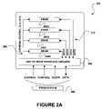
- FIGS. 2A-Eshow a stack of DRAM circuits 200 that utilize one or more interface circuits, in accordance with various embodiments.
- the stack of DRAM circuits 200may be implemented in the context of the architecture of FIG. 1 .
- the stack of DRAM circuits 200may be implemented in any other desired environment (e.g. using other memory types, using different memory types within a stack, etc.). It should also be noted that the aforementioned definitions may apply during the present description.
- one or more interface circuits 202may be placed electrically between an electronic system 204 and a stack of DRAM circuits 206 A-D.
- the interface circuits 202electrically sit between the electronic system 204 and the stack of DRAM circuits 206 A-D.
- the interface circuit(s) 202may include any interface circuit that meets the definition set forth during reference to FIG. 1 .
- the interface circuit(s) 202may be capable of interfacing (e.g. buffering, etc.) the stack of DRAM circuits 206 A-D to electrically and/or logically resemble at least one larger capacity virtual DRAM circuit to the system 204 .
- a stack or buffered stackmay be utilized. In this way, the stack of DRAM circuits 206 A-D may appear as a smaller quantity of larger capacity virtual DRAM circuits to the system 204 .
- the stack of DRAM circuits 206 A-Dmay include eight 512 Mb DRAM circuits.
- the interface circuit(s) 202may buffer the stack of eight 512 Mb DRAM circuits to resemble a single 4 Gb virtual DRAM circuit to a memory controller (not shown) of the associated system 204 .
- the interface circuit(s) 202may buffer the stack of eight 512 Mb DRAM circuits to resemble two 2 Gb virtual DRAM circuits to a memory controller of an associated system 204 .
- the stack of DRAM circuits 206 A-Dmay include any number of DRAM circuits.
- the interface circuit(s) 202may be connected to 1, 2, 4, 8 or more DRAM circuits 206 A-D.
- the interface circuit(s) 202may be connected to an odd number of DRAM circuits 206 A-D.
- the DRAM circuits 206 A-Dmay be arranged in a single stack. Of course, however, the DRAM circuits 206 A-D may also be arranged in a plurality of stacks
- the DRAM circuits 206 A-Dmay be arranged on, located on, or connected to a single side of the interface circuit(s) 202 , as shown in FIGS. 2A-D . As another option, the DRAM circuits 206 A-D may be arranged on, located on, or connected to both sides of the interface circuit(s) 202 shown in FIG. 2E .
- the interface circuit(s) 202may be connected to 16 DRAM circuits with 8 DRAM circuits on either side of the interface circuit(s) 202 , where the 8 DRAM circuits on each side of the interface circuit(s) 202 are arranged in two stacks of four DRAM circuits. In other embodiments, other arrangements and numbers of DRAM circuits are possible (e.g. to implement error-correction coding, ECC, etc.)
- the interface circuit(s) 202may optionally be a part of the stack of DRAM circuits 206 A-D. Of course, however, interface circuit(s) 202 may also be separate from the stack of DRAM circuits 206 A-D. In addition, interface circuit(s) 202 may be physically located anywhere in the stack of DRAM circuits 206 A-D, where such interface circuit(s) 202 electrically sits between the electronic system 204 and the stack of DRAM circuits 206 A-D.
- the interface circuit(s) 202may be located at the bottom of the stack of DRAM circuits 206 A-D (e.g. the bottom-most circuit in the stack) as shown in FIGS. 2A-2D .
- the interface circuit(s) 202may be located in the middle of the stack of DRAM circuits 206 A-D.
- the interface circuit(s) 202may be located at the top of the stack of DRAM circuits 206 A-D (e.g. the top-most circuit in the stack).
- the interface circuit(s) 202may also be located anywhere between the two extremities of the stack of DRAM circuits 206 A-D.
- the interface circuit(s) 202may not be in the stack of DRAM circuits 206 A-D and may be located in a separate package(s).
- the electrical connections between the interface circuit(s) 202 and the stack of DRAM circuits 206 A-Dmay be configured in any desired manner.
- address, control (e.g. command, etc.), and clock signalsmay be common to all DRAM circuits 206 A-D in the stack (e.g. using one common bus).
- each DRAM circuit 206 A-Dthere may be individual address, control and clock busses to each DRAM circuit 206 A-D.
- data signalsmay be wired as one common bus, several busses, or as an individual bus to each DRAM circuit 206 A-D.
- any combinations of such configurationsmay also be utilized.
- the DRAM circuits 206 A-Dmay have one common address, control and clock bus 208 with individual data busses 210 .
- the DRAM circuits 206 A-Dmay have two address, control and clock busses 208 along with two data busses 210 .
- the DRAM circuits 206 A-Dmay have one address, control and clock bus 208 together with two data busses 210 .
- the DRAM circuits 206 A-Dmay have one common address, control and clock bus 208 and one common data bus 210 . It should be noted that any other permutations and combinations of such address, control, clock and data buses may be utilized.
- the interface circuit(s) 202may be split into several chips that, in combination, perform power management functions. Such power management functions may optionally introduce a delay in various signals.
- register chipthere may be a single register chip that electrically sits between a memory controller and a number of stacks of DRAM circuits.
- the register chipmay, for example, perform the signaling to the DRAM circuits.
- Such register chipmay be connected electrically to a number of other interface circuits that sit electrically between the register chip and the stacks of DRAM circuits. Such interface circuits in the stacks of DRAM circuits may then perform the aforementioned delay, as needed.
- each DRAM stackthere may be no need for an interface circuit in each DRAM stack.
- the register chipmay perform the signaling to the DRAM circuits directly.
- each stackmay be a single memory (e.g. DRAM) circuit.
- combinations of the above implementationsmay be used.
- register chipsmay be used in combination with other interface circuits, or registers may be utilized alone.
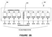
- FIGS. 3A-Dshow a memory module 300 which uses DRAM circuits or stacks of DRAM circuits (e.g. DRAM stacks) with various interface circuits, in accordance with different embodiments.
- the memory module 300may be implemented in the context of the architecture and environment of FIGS. 1 and/or 2 . Of course, however, the memory module 300 may be implemented in any desired environment. It should also be noted that the aforementioned definitions may apply during the present description.
- FIG. 3Ashows two register chips 304 driving address and control signals to DRAM circuits 302 .
- the DRAM circuits 302may send/receive data signals to and/or from a system (e.g. memory controller) using the DRAM data bus, as shown.
- a systeme.g. memory controller
- FIG. 3Bshows one register chip 304 driving address and control signals to DRAM circuits 302 .
- register chips 304may be utilized, in various embodiments.
- FIG. 3Cshows register chips 304 driving address and control signals to DRAM circuits 302 and/or intelligent interface circuits 303 .
- the DRAM data busis connected to the intelligent interface circuits 303 (not shown explicitly).
- the register chip(s) 304may drive some, all, or none of the control and/or address signals to intelligent interface circuits 303 .
- FIG. 3Dshows register chips 304 driving address and control signals to the DRAM circuits 302 and/or intelligent interface circuits 303 .
- the register chip(s) 304may drive some, all, or none of the control and/or address signals to intelligent interface circuits 303 .
- the DRAM data busis connected to the intelligent interface circuits 303 .
- this figureillustrates that either one (in the case of DRAM stack 306 ) or two (in the case of the other DRAM stacks 302 ) stacks of DRAM circuits 302 may be associated with a single intelligent interface circuit 303 .
- any number of stacks of DRAM circuits 302may be associated with each intelligent interface circuit 303 .
- an AMB chipmay be utilized with an FB-DIMM, as will be described in more detail with respect to FIGS. 4A-E .
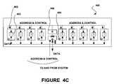
- FIGS. 4A-Eshow a memory module 400 which uses DRAM circuits or stacks of DRAM circuits (e.g. DRAM stacks) 402 with an AMB chip 404 , in accordance with various embodiments.
- the memory module 400may be implemented in the context of the architecture and environment of FIGS. 1-3 . Of course, however, the memory module 400 may be implemented in any desired environment. It should also be noted that the aforementioned definitions may apply during the present description.
- FIG. 4Ashows the AMB chip 404 driving address and control signals to the DRAM circuits 402 .
- the AMB chip 404sends/receives data to/from the DRAM circuits 402 .
- FIG. 4Bshows the AMB chip 404 driving address and control signals to a register 406 .
- the register 406may drive address and control signals to the DRAM circuits 402 .
- the DRAM circuitssend/receive data to/from the AMB.
- a DRAM data busmay be connected to the AMB chip 404 .
- FIG. 4Cshows the AMB chip 404 driving address and control to the register 406 .
- the register 406may drive address and control signals to the DRAM circuits 402 and/or the intelligent interface circuits 403 .
- This figureillustrates that the register 406 may drive zero, one, or more address and/or control signals to one or more intelligent interface circuits 403 .
- each DRAM data busis connected to the interface circuit 403 (not shown explicitly).
- the intelligent interface circuit data busis connected to the AMB chip 404 .
- the AMB data busis connected to the system.
- FIG. 4Dshows the AMB chip 404 driving address and/or control signals to the DRAM circuits 402 and/or the intelligent interface circuits 403 .
- This figureillustrates that the AMB chip 404 may drive zero, one, or more address and/or control signals to one or more intelligent interface circuits 403 .
- each DRAM data busis connected to the intelligent interface circuits 403 (not shown explicitly).
- the intelligent interface circuit data busis connected to the AMB chip 404 .
- the AMB data busis connected to the system.
- FIG. 4Eshows the AMB chip 404 driving address and control to one or more intelligent interface circuits 403 .
- the intelligent interface circuits 403then drive address and control to each DRAM circuit 402 (not shown explicitly).
- each DRAM data busis connected to the intelligent interface circuits 403 (also not shown explicitly).
- the intelligent interface circuit data busis connected to the AMB chip 404 .
- the AMB data busis connected to the system.
- register chipsmay be utilized in conjunction with the intelligent interface circuits.
- register chipsmay be utilized alone and/or with or without stacks of DRAM circuits.
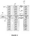
- FIG. 5shows a system 500 in which four 512 Mb DRAM circuits appear, through simulation, as (e.g. mapped to) a single 2 Gb virtual DRAM circuit, in accordance with yet another embodiment.
- the system 500may be implemented in the context of the architecture and environment of FIGS. 1-4 . Of course, however, the system 500 may be implemented in any desired environment. It should also be noted that the aforementioned definitions may apply during the present description.
- a stack of memory circuits that is interfaced by the interface circuit for the purpose of simulationmay include four 512 Mb physical DRAM circuits 502 A-D that appear to a memory controller as a single 2 Gb virtual DRAM circuit.
- the buffered stackmay include various numbers of physical DRAM circuits including two, four, eight, sixteen or even more physical DRAM circuits that appear to the memory controller as a single larger capacity virtual DRAM circuit or multiple larger capacity virtual DRAM circuits.
- the number of physical DRAM circuits in the buffered stackmay be an odd number. For example, an odd number of circuits may be used to provide data redundancy or data checking or other features.
- one or more control signals (e.g. power management signals) 506may be connected between the interface circuit 504 and the DRAM circuits 502 A-D in the stack.
- the interface circuit 504may be connected to a control signal (e.g. power management signal) 508 from the system, where the system uses the control signal 508 to control one aspect (e.g. power behavior) of the 2 Gb virtual DRAM circuit in the stack.
- the interface circuit 504may control the one aspect (e.g. power behavior) of all the DRAM circuits 502 A-D in response to a control signal 508 from the system to the 2 Gb virtual DRAM circuit.
- the interface circuit 504may also, using control signals 506 , control the one aspect (e.g. power behavior) of one or more of the DRAM circuits 502 A-D in the stack in the absence of a control signal 508 from the system to the 2 Gb virtual DRAM circuit.
- the buffered stacks 500may also be used in combination together on a DIMM such that the DIMM appears to the memory controller as a larger capacity DIMM.
- the buffered stacksmay be arranged in one or more ranks on the DIMM. All the virtual DRAM circuits on the DIMM that respond in parallel to a control signal 508 (e.g. chip select signal, clock enable signal, etc.) from the memory controller belong to a single rank.
- the interface circuit 504may use a plurality of control signals 506 instead of control signal 508 to control DRAM circuits 502 A-D.
- the interface circuit 504may use all the control signals 506 in parallel in response to the control signal 508 to do power management of the DRAM circuits 502 A-D in one example.
- the interface circuit 504may use at least one but not all the control signals 506 in response to the control signal 508 to do power management of the DRAM circuits 502 A-D. In yet another example, the interface circuit 504 may use at least one control signal 506 in the absence of the control signal 508 to do power management of the DRAM circuits 502 A-D.
- the number of banks per DRAM circuitmay be defined by JEDEC standards for many DRAM circuit technologies.
- multiple physical DRAM circuits 502 A-Dmay be stacked and interfaced by an interface circuit 504 and may appear as at least one larger capacity virtual DRAM circuit to the memory controller.
- the stackmay include four 512 Mb DDR2 physical SDRAM circuits that appear to the memory controller as a single 2 Gb virtual DDR2 SDRAM circuit.
- each bank of a virtual DRAM circuit seen by the memory controllermay correspond to a portion of a physical DRAM circuit. That is, each physical DRAM circuit may be mapped to multiple banks of a virtual DRAM circuit. For example, in one embodiment, four 512 Mb DDR2 physical SDRAM circuits through simulation may appear to the memory controller as a single 2 Gb virtual DDR2 SDRAM circuit. A 2 Gb DDR2 SDRAM may have eight banks as specified by the JEDEC standards. Therefore, in this embodiment, the interface circuit 504 may map each 512 Mb physical DRAM circuit to two banks of the 2 Gb virtual DRAM. Thus, in the context of the present embodiment, a one-circuit-to-many-bank configuration (one physical DRAM circuit to many banks of a virtual DRAM circuit) may be utilized.
- each physical DRAM circuitmay be mapped to a single bank of a virtual DRAM circuit.
- eight 512 Mb DDR2 physical SDRAM circuitsmay appear to the memory controller, through simulation, as a single 4 Gb virtual DDR2 SDRAM circuit.
- a 4 Gb DDR2 SDRAMmay have eight banks as specified by the JEDEC standards. Therefore, the interface circuit 504 may map each 512 Mb physical DRAM circuit to a single bank of the 4 Gb virtual DRAM. In this way, a one-circuit-to-one-bank configuration (one physical DRAM circuit to one bank of a virtual DRAM circuit) may be utilized.
- a plurality of physical DRAM circuitsmay be mapped to a single bank of a virtual DRAM circuit.
- sixteen 256 Mb DDR2 physical SDRAM circuitsmay appear to the memory controller, through simulation, as a single 4 Gb virtual DDR2 SDRAM circuit.
- a 4 Gb DDR2 SDRAM circuitmay be specified by JEDEC to have eight banks, such that each bank of the 4 Gb DDR2 SDRAM circuit may be 512 Mb.
- two of the 256 Mb DDR2 physical SDRAM circuitsmay be mapped by the interface circuit 504 to a single bank of the 4 Gb virtual DDR2 SDRAM circuit seen by the memory controller. Accordingly, a many-circuit-to-one-bank configuration (many physical DRAM circuits to one bank of a virtual DRAM circuit) may be utilized.
- multiple physical DRAM circuits 502 A-D in the stackmay be buffered by the interface circuit 504 and may appear as at least one larger capacity virtual DRAM circuit to the memory controller.
- the buffered stackmay include four 512 Mb DDR2 physical SDRAM circuits that appear to the memory controller as a single 2 Gb DDR2 virtual SDRAM circuit.
- the combined power dissipation of all four DRAM circuits 502 A-D in the stack when they are activemay be higher than the power dissipation of a monolithic (e.g. constructed without stacks) 2 Gb DDR2 SDRAM.
- the power dissipation of a DIMM constructed from buffered stacksmay be much higher than a DIMM constructed without buffered stacks.
- a DIMM containing multiple buffered stacksmay dissipate much more power than a standard DIMM built using monolithic DRAM circuits.
- power managementmay be utilized to reduce the power dissipation of DIMMs that contain buffered stacks of DRAM circuits.
- power management schemesmay be utilized for one-circuit-to-many-bank, one-circuit-to-one-bank, and many-circuit-to-one-bank configurations.
- Memorye.g. DRAM
- DDR2 SDRAMfor example, power management may be initiated using the CKE and chip select (CS#) inputs and optionally in combination with a command to place the DDR2 SDRAM in various power down modes.
- CS#chip select
- DDR2 SDRAMFour power saving modes for DDR2 SDRAM may be utilized, in accordance with various different embodiments (or even in combination, in other embodiments).
- two active power down modes, precharge power down mode, and self-refresh modemay be utilized. If CKE is de-asserted while CS# is asserted, the DDR2 SDRAM may enter an active or precharge power down mode. If CKE is de-asserted while CS# is asserted in combination with the refresh command, the DDR2 SDRAM may enter the self refresh mode.
- the DDR2 SDRAMmay enter precharge power down mode. If power down occurs when there are no rows active in any bank, the DDR2 SDRAM may enter one of the two active power down modes.
- the two active power down modesmay include fast exit active power down mode or slow exit active power down mode.
- the selection of fast exit mode or slow exit modemay be determined by the configuration of a mode register.
- the maximum duration for either the active power down mode or the precharge power down modemay be limited by the refresh requirements of the DDR2 SDRAM and may further be equal to tRFC(MAX).
- DDR2 SDRAMsmay require CKE to remain stable for a minimum time of tCKE(MIN). DDR2 SDRAMs may also require a minimum time of tXP(MIN) between exiting precharge power down mode or active power down mode and a subsequent non-read command. Furthermore, DDR2 SDRAMs may also require a minimum time of tXARD(MIN) between exiting active power down mode (e.g. fast exit) and a subsequent read command. Similarly, DDR2 SDRAMs may require a minimum time of tXARDS(MIN) between exiting active power down mode (e.g. slow exit) and a subsequent read command.
- the SDRAMmay require a power down entry latency of three clock cycles.
- the SDRAMmay require a power down exit latency of two clock cycles.
- the power down entry latency and power down exit latencymay be different, but this does not necessarily affect the operation of power management described here.
- a minimum total of five clock cyclesmay be required to enter and then immediately exit a power down mode (e.g. three cycles to satisfy tCKE(min) due to entry latency plus two cycles to satisfy tXP(MIN) or tXARD(MIN) due to exit latency). These five clock cycles may be hidden from the memory controller if power management is not being performed by the controller itself.
- tCKE(min)due to entry latency plus two cycles to satisfy tXP(MIN) or tXARD(MIN) due to exit latency
- tXP(MIN)tXARD(MIN) due to exit latency
- the minimum power down entry latency for a DRAM circuitmay be n clocks.
- the minimum power down exit latency of a DRAM circuitmay be x clocks.
- DRAM operationssuch as precharge or activate may require a certain period of time to complete.
- the DRAM, or portion(s) thereof (e.g. bank, etc.) to which the operation is directedmay be unable to perform another operation.
- a precharge operation in a bank of a DRAM circuitmay require a certain period of time to complete (specified as tRP for DDR2).
- the memory controllermay not necessarily be allowed to direct another operation (e.g. activate, etc.) to the same bank of the DRAM circuit.
- the period of time between the initiation of an operation and the completion of that operationmay thus be a command operation period.
- the memory controllermay not necessarily be allowed to direct another operation to a particular DRAM circuit or portion thereof during a command operation period of various commands or operations.
- the command operation period of a precharge operation or commandmay be equal to tRP.
- the command operation period of an activate commandmay be equal to tRCD.
- the command operation periodneed not be limited to a single command.
- a command operation periodcan also be defined for a sequence, combination, or pattern of commands.
- the power management schemes described hereinthus need not be limited to a single command and associated command operation period; the schemes may equally be applied to sequences, patterns, and combinations of commands.
- a commandmay have a first command operation period in a DRAM circuit to which the command is directed to, and also have a second command operation period in another DRAM circuit to which the command is not directed to.
- the first and second command operation periodsneed not be the same.
- a commandmay have different command operation periods in different mappings of physical DRAM circuits to the banks of a virtual DRAM circuit, and also under different conditions.
- command operation periodsmay be specified in nanoseconds.
- tRPmay be specified in nanoseconds, and may vary according to the speed grade of a DRAM circuit.
- tRPmay be defined in JEDEC standards (e.g. currently JEDEC Standard No. 21-C for DDR2 SDRAM).
- JEDEC standardse.g. currently JEDEC Standard No. 21-C for DDR2 SDRAM.
- tRPmay be measured as an integer number of clock cycles.
- the tRPmay not necessarily be specified to be an exact number clock cycles.
- the minimum value of tRPmay be equivalent to three clock cycles or more.
- power management schemesmay be based on an interface circuit identifying at least one memory (e.g. DRAM, etc.) circuit that is not currently being accessed by the system.
- a power saving operationmay be initiated in association with the at least one memory circuit.
- such power saving operationmay involve a power down operation, and in particular, a precharge power down operation, using the CKE pin of the DRAM circuits (e.g. a CKE power management scheme).
- a power down operationand in particular, a precharge power down operation, using the CKE pin of the DRAM circuits (e.g. a CKE power management scheme).
- Other similar power management schemesusing other power down control methods and power down modes, with different commands and alternative memory circuit technologies, may also be used.
- the presence of the schememay be transparent to the memory controller. Accordingly, the power down entry latency and the power down exit latency may be hidden from the memory controller. In one embodiment, the power down entry and exit latencies may be hidden from the memory controller by opportunistically placing at least one first DRAM circuit into a power down mode and, if required, bringing at least one second DRAM circuit out of power down mode during a command operation period when the at least one first DRAM circuit is not being accessed by the system.
- the identification of the appropriate command operation period during which at least one first DRAM circuit in a stack may be placed in power down mode or brought out of power down modemay be based on commands directed to the first DRAM circuit (e.g. based on commands directed to itself) or on commands directed to a second DRAM circuit (e.g. based on commands directed to other DRAM circuits).
- the command operation period of the DRAM circuitmay be used to hide the power down entry and/or exit latencies.
- the existing command operation periods of the physical DRAM circuitsmay be used to the hide the power down entry and/or exit latencies if the delays associated with one or more operations are long enough to hide the power down entry and/or exit latencies.
- the command operation period of a virtual DRAM circuitmay be used to hide the power down entry and/or exit latencies by making the command operation period of the virtual DRAM circuit longer than the command operation period of the physical DRAM circuits.
- the interface circuitmay simulate a plurality of physical DRAM circuits to appear as at least one virtual DRAM circuit with at least one command operation period that is different from that of the physical DRAM circuits.
- This embodimentmay be used if the existing command operation periods of the physical DRAM circuits are not long enough to hide the power down entry and/or exit latencies, thus necessitating the interface circuit to increase the command operation periods by simulating a virtual DRAM circuit with at least one different (e.g. longer, etc.) command operation period from that of the physical DRAM circuits.
- Row cycle time based power managementis an example of a power management scheme that uses the command operation period of DRAM circuits to hide power down entry and exit latencies.
- the interface circuitmay place at least one first physical DRAM circuit into power down mode based on the commands directed to a second physical DRAM circuit.
- Power management schemessuch as a row cycle time based scheme may be best suited for a many-circuit-to-one-bank configuration of DRAM circuits.
- a plurality of physical DRAM circuitsmay be mapped to a single bank of a larger capacity virtual DRAM circuit seen by the memory controller.
- sixteen 256 Mb DDR2 physical SDRAM circuitsmay appear to the memory controller as a single 4 Gb virtual DDR2 SDRAM circuit. Since a 4 Gb DDR2 SDRAM circuit is specified by the JEDEC standards to have eight physical banks, two of the 256 Mb DDR2 physical SDRAM circuits may be mapped by the interface circuit to a single bank of the virtual 4 Gb DDR2 SDRAM circuit.
- bank 0 of the virtual 4 Gb DDR2 SDRAM circuitmay be mapped by the interface circuit to two 256 Mb DDR2 physical SDRAM circuits (e.g. DRAM A and DRAM B).
- DRAM A and DRAM B256 Mb DDR2 physical SDRAM circuits
- bank 0 of the virtual 4 Gb DDR2 SDRAM circuitmay be mapped by the interface circuit to two 256 Mb DDR2 physical SDRAM circuits (e.g. DRAM A and DRAM B).
- DRAM A and DRAM B256 Mb DDR2 physical SDRAM circuits
- the memory controllermay be unable to issue a second activate command to bank 0 of the 4 Gb virtual DRAM until a period tRC has elapsed from the time the first activate command was issued by the memory controller.
- the command operation period of an activate commandmay be tRC.
- the parameter tRCmay be much longer than the power down entry and exit latencies.
- the interface circuitmay place DRAM B in the precharge power down mode during the activate command operation period (e.g. for period tRC).
- the first activate commandis directed by the interface circuit to DRAM B, then it may place DRAM A in the precharge power down mode during the command operation period of the first activate command.
- the power saving operationmay, for example, comprise operating in precharge power down mode except when refresh is required. Of course, power savings may also occur in other embodiments without such continuity.
- Row precharge time based power managementis an example of a power management scheme that, in one embodiment, uses the precharge command operation period (that is the command operation period of precharge commands, tRP) of physical DRAM circuits to hide power down entry and exit latencies.
- a row precharge time based power management schememay be implemented that uses the precharge command operation period of virtual DRAM circuits to hide power down entry and exit latencies.
- the interface circuitmay place at least one DRAM circuit into power down mode based on commands directed to the same at least one DRAM circuit.
- Power management schemessuch as the row precharge time based scheme may be best suited for many-circuit-to-one-bank and one-circuit-to-one-bank configurations of physical DRAM circuits.
- a row precharge time based power management schememay be particularly efficient when the memory controller implements a closed page policy.
- a row precharge time based power management schememay power down a physical DRAM circuit after a precharge or autoprecharge command closes an open bank. This power management scheme allows each physical DRAM circuit to enter power down mode when not in use. While the specific memory circuit technology used in this example is DDR2 and the command used here is the precharge or autoprecharge command, the scheme may be utilized in any desired context. This power management scheme uses an algorithm to determine if there is any required delay as well as the timing of the power management in terms of the command operation period.
- the interface circuitmay place that DRAM circuit into precharge power down mode during the command operation period of the precharge or autoprecharge command.
- the precharge power down modemay be initiated following the precharge or autoprecharge command to the open bank in that physical DRAM circuit.
- the physical DRAM circuitmay be brought out of precharge power down mode before the earliest time a subsequent activate command may arrive at the inputs of the physical DRAM circuit.
- the power down entry and power down exit latenciesmay be hidden from the memory controller.
- a plurality of physical DRAM circuitsmay appear to the memory controller as at least one larger capacity virtual DRAM circuit with a tRP(virtual) that is larger than that of the physical DRAM circuits [e.g. larger than tRP(physical)].
- the physical DRAM circuitsmay, through simulation, appear to the memory controller as a larger capacity virtual DRAM with tRP(virtual) equal to tRP(physical)+m, where m may be an integer multiple of the clock cycle, or may be a non-integer multiple of the clock cycle, or may be a constant or variable multiple of the clock cycle, or may be less than one clock cycle, or may be zero. Note that m may or may not be equal to j.
- the interface circuitmay place a physical DRAM circuit into precharge power down mode in a subsequent clock cycle after a precharge or autoprecharge command to the open bank in the physical DRAM circuit has been received by the physical DRAM circuit. Additionally, the physical DRAM circuit may be brought out of precharge power down mode before the earliest time a subsequent activate command may arrive at the inputs of the physical DRAM circuit. Thus, the power down entry and power down exit latency may be hidden from the memory controller.
- the interface circuitmay make the stack of physical DRAM circuits appear to the memory controller as at least one larger capacity virtual DRAM circuit with tRP(virtual) and tRCD(virtual) that are larger than that of the physical DRAM circuits in the stack [e.g. larger than tRP(physical) and tRCD(physical) respectively, where tRCD(physical) is the tRCD of the physical DRAM circuits].
- the stack of physical DRAM circuitsmay appear to the memory controller as a larger capacity virtual DRAM with tRP(virtual) and tRCD(virtual) equal to [tRP(physical)+m] and tRCD(physical)+l] respectively.
- lmay be an integer multiple of the clock cycle, or may be a non-integer multiple of the clock cycle, or may be constant or variable multiple of the clock cycle, or may be less than a clock cycle, or may be zero. Also, l may or may not be equal to j and/or m.
- the interface circuitmay use the following sequence of events to implement a row precharge time based power management scheme and also hide the power down entry and exit latencies from the memory controller.
- the interface circuitmay place that physical DRAM circuit into precharge power down mode in a subsequent clock cycle after the precharge or autoprecharge command has been received by that physical DRAM circuit.
- the interface circuitmay continue to keep the physical DRAM circuit in the precharge power down mode until the interface circuit receives a subsequent activate command to that physical DRAM circuit.
- the interface circuitmay then bring the physical DRAM circuit out of precharge power down mode by asserting the CKE input of the physical DRAM in a following clock cycle.
- the interface circuitmay also delay the address and control signals associated with the activate command for a minimum of x clock cycles before sending the signals associated with the activate command to the physical DRAM circuit.
- the row precharge time based power management scheme described aboveis suitable for many-circuit-to-one-bank and one-circuit-to-one-bank configurations since there is a guaranteed minimum period of time (e.g. a keep-out period) of at least tRP(physical) after a precharge command to a physical DRAM circuit during which the memory controller will not issue a subsequent activate command to the same physical DRAM circuit.
- the command operation period of a precharge commandapplies to the entire DRAM circuit.
- a precharge command to a first portion(s)e.g.
- the interface circuitmay map two banks of the 2 Gb virtual DRAM circuit to each 512 Mb physical DRAM circuit.
- banks 0 and 1 of the 2 Gb virtual DRAM circuitmay be mapped to a single 512 Mb physical DRAM circuit (e.g. DRAM C).
- bank 0 of the virtual DRAM circuitmay have an open page while bank 1 of the virtual DRAM circuit may have no open page.
- the interface circuitmay signal DRAM C to enter the precharge power down mode after the precharge or autoprecharge command has been received by DRAM C.
- the interface circuitmay accomplish this by de-asserting the CKE input of DRAM C during a clock cycle subsequent to the clock cycle in which DRAM C received the precharge or autoprecharge command.
- the memory controllermay issue an activate command to the bank 1 of the 2 Gb virtual DRAM circuit on the next clock cycle after it issued the precharge command to bank 0 of the virtual DRAM circuit.
- DRAM Cmay have just entered a power down mode and may need to exit power down immediately.
- the command operation period of the precharge command to bank 0 of the 2 Gb virtual DRAM circuitmay not be sufficiently long enough to hide the power down entry latency of DRAM C even if the command operation period of the activate command to bank 1 of the 2 Gb virtual DRAM circuit is long enough to hide the power down exit latency of DRAM C, which would then cause the simulated 2 Gb virtual DRAM circuit to not be in compliance with the DDR2 protocol. It is therefore difficult, in a simple fashion, to hide the power management latency during the command operation period of precharge commands in a one-circuit-to-many-bank configuration.
- Row activate time based power managementis a power management scheme that, in one embodiment, may use the activate command operation period (that is the command operation period of activate commands) of DRAM circuits to hide power down entry latency and power down exit latency.
- a row activate time based power management schememay be used for many-circuit-to-one-bank and one-circuit-to-one-bank configurations.
- the power down entry and exit latencies of a physical DRAM circuitmay be hidden behind the command operation period of an activate command directed to itself.
- the command operation period of an activate commandmay be tRCD.
- a row activate time based power management schememay place a first DRAM circuit that has no open banks into a power down mode when an activate command is issued to a second DRAM circuit if the first and second DRAM circuits are part of a plurality of physical DRAM circuits that appear as a single virtual DRAM circuit to the memory controller.
- This power management schememay allow each DRAM circuit to enter power down mode when not in use.
- This embodimentmay be used in one-circuit-to-many-bank configurations of DRAM circuits. While the specific memory circuit technology used in this example is DDR2 and the command used here is the activate command, the scheme may be utilized in any desired context. The scheme uses an algorithm to determine if there is any required delay as well as the timing of the power management in terms of the command operation period.
- a plurality of banks of a virtual DRAM circuitmay be mapped to a single physical DRAM circuit.
- four 512 Mb DDR2 SDRAM circuits through simulationmay appear to the memory controller as a single 2 Gb virtual DDR2 SDRAM circuit with eight banks. Therefore, the interface circuit may map two banks of the 2 Gb virtual DRAM circuit to each 512 Mb physical DRAM circuit.
- banks 0 and 1 of the 2 Gb virtual DRAM circuitmay be mapped to a first 512 Mb physical DRAM circuit (e.g. DRAM P).
- banks 2 and 3 of the 2 Gb virtual DRAM circuitmay be mapped to a second 512 Mb physical DRAM circuit (e.g.
- banks 4 and 5 of the 2 Gb virtual DRAM circuitmay be mapped to a third 512 Mb physical DRAM circuit (e.g. DRAM R), and banks 6 and 7 of the 2 Gb virtual DRAM circuit may be mapped to a fourth 512 Mb physical DRAM circuit (e.g. DRAM S).
- a third 512 Mb physical DRAM circuite.g. DRAM R
- banks 6 and 7 of the 2 Gb virtual DRAM circuitmay be mapped to a fourth 512 Mb physical DRAM circuit (e.g. DRAM S).
- bank 0 of the virtual DRAM circuitmay have an open page while all the other banks of the virtual DRAM circuit may have no open pages.
- the interface circuitmay not be able to place DRAM P in precharge power down mode after the precharge or autoprecharge command has been received by DRAM P. This may be because the memory controller may issue an activate command to bank 1 of the 2 Gb virtual DRAM circuit in the very next cycle.
- a row precharge time based power management schememay not be used in a one-circuit-to-many-bank configuration since there is no guaranteed keep-out period after a precharge or autoprecharge command to a physical DRAM circuit.
- the memory controllermay ensure a minimum period of time, tRRD(MIN), between activate commands to the single 2 Gb virtual DRAM circuit.
- tRRD(MIN)a minimum period of time between activate commands to the single 2 Gb virtual DRAM circuit.
- the active bank N to active bank M command period tRRDmay be variable with a minimum value of tRRD(MIN) (e.g. 2 clock cycles, etc.).
- the parameter tRRDmay be specified in nanoseconds and may be defined in JEDEC Standard No. 21-C.
- tRRDmay be measured as an integer number of clock cycles.
- tRRDmay not be specified to be an exact number of clock cycles.
- the tRRD parametermay mean an activate command to a second bank B of a DRAM circuit (either physical DRAM circuit or virtual DRAM circuit) may not be able to follow an activate command to a first bank A of the same DRAM circuit in less than tRRD clock cycles.
- a first number of physical DRAM circuits that have no open pagesmay be placed in power down mode when an activate command is issued to another physical DRAM circuit that through simulation is part of the same virtual DRAM circuit.
- the interface circuitmay keep DRAM P in precharge standby mode until the memory controller issues an activate command to one of DRAM Q, DRAM R, and DRAM S.
- the interface circuitmay then immediately place DRAM P into precharge power down mode if tRRD(MIN) ⁇ n.
- the additional typical one clock cycle delay through a JEDEC registerhelps to hide the power down entry latency if tRRD(MIN) by itself is not sufficiently long to hide the power down entry latency.
- a row activate time power management schemerequire l to be larger than or equal to x (where x is the power down exit latency) so that when the memory controller issues an activate command to a bank of the virtual DRAM circuit, and if the corresponding physical DRAM circuit is in precharge power down mode, the interface circuit can hide the power down exit latency of the physical DRAM circuit behind the row activate time tRCD of the virtual DRAM circuit.
- the interface circuitwhen the interface circuit receives an activate command that is directed to a DRAM circuit that is in precharge power down mode, it will delay the activate command by at least x clock cycles while simultaneously bringing the DRAM circuit out of power down mode. Since l ⁇ x, the command operation period of the activate command may overlap the power down exit latency, thus allowing the interface circuit to hide the power down exit latency behind the row activate time.
- DRAM Pmay be placed into precharge power down mode after the memory controller issued a precharge or autoprecharge command to the last open page in DRAM P and then issued an activate command to one of DRAM Q, DRAM R, and DRAM S.
- the interface circuitmay immediately bring DRAM P out of precharge power down mode while delaying the activate command to DRAM P by at least x clock cycles. Since l ⁇ x, DRAM P may be ready to receive the delayed activate command when the interface circuit sends the activate command to DRAM P.
- each physical DRAM circuitis mapped to one bank (or portion(s) thereof) of a larger capacity virtual DRAM circuit, it may be certain that no command may be issued to a physical DRAM circuit for a minimum of tRCD(virtual) clock cycles after an activate command has been issued to the physical DRAM circuit.
- the interface circuitmay place the physical DRAM circuit into active power down mode on the clock cycle after the activate command has been received by the physical DRAM circuit and bring the physical DRAM circuit out of active power down mode before the earliest time a subsequent read or write command may arrive at the inputs of the physical DRAM circuit.
- the power down entry and power down exit latenciesmay be hidden from the memory controller.
- the command and power down mode used for the activate command based power-management schememay be the activate command and precharge or active power down modes, but other similar power down schemes may use different power down modes, with different commands, and indeed even alternative DRAM circuit technologies may be used.
- Refresh cycle time based power managementis a power management scheme that uses the refresh command operation period (that is the command operation period of refresh commands) of virtual DRAM circuits to hide power down entry and exit latencies.
- the interface circuitplaces at least one physical DRAM circuit into power down mode based on commands directed to a different physical DRAM circuit.
- a refresh cycle time based power management scheme that uses the command operation period of virtual DRAM circuitsmay be used for many-circuit-to-one-bank, one-circuit-to-one-bank, and one-circuit-to-many-bank configurations.
- Refresh commands to a DRAM circuitmay have a command operation period that is specified by the refresh cycle time, tRFC.
- the minimum and maximum values of the refresh cycle time, tRFCmay be specified in nanoseconds and may further be defined in the JEDEC standards (e.g. JEDEC Standard No. 21-C for DDR2 SDRAM, etc.).
- the minimum value of tRFCe.g. tRFC(MIN)] may vary as a function of the capacity of the DRAM circuit. Larger capacity DRAM circuits may have larger values of tRFC(MIN) than smaller capacity DRAM circuits.
- the parameter tRFCmay be measured as an integer number of clock cycles, although optionally the tRFC may not be specified to be an exact number clock cycles.
- a memory controllermay initiate refresh operations by issuing refresh control signals to the DRAM circuits with sufficient frequency to prevent any loss of data in the DRAM circuits.
- a minimum timee.g. denoted by tRFC
- tRFCrefresh cycle time
- the interface circuitWhen the interface circuit receives a refresh command from the memory controller, it may refresh the smaller capacity physical DRAM circuits within the span of time specified by the tRFC associated with the larger capacity virtual DRAM circuit. Since the tRFC of the virtual DRAM circuit may be larger than that of the associated physical DRAM circuits, it may not be necessary to issue refresh commands to all of the physical DRAM circuits simultaneously. Refresh commands may be issued separately to individual physical DRAM circuits or may be issued to groups of physical DRAM circuits, provided that the tRFC requirement of the physical DRAM circuits is satisfied by the time the tRFC of the virtual DRAM circuit has elapsed.
- the interface circuitmay place a physical DRAM circuit into power down mode for some period of the tRFC of the virtual DRAM circuit when other physical DRAM circuits are being refreshed.
- four 512 Mb physical DRAM circuitse.g. DRAM W, DRAM X, DRAM Y, DRAM Z
- the memory controllerissues a refresh command to the 2 Gb virtual DRAM circuit, it may not issue another command to the 2 Gb virtual DRAM circuit at least until a period of time, tRFC(MIN)(virtual), has elapsed.
- the interface circuitmay stagger the refresh commands to DRAM W, DRAM X, DRAM Y, DRAM Z such that that total time needed to refresh all the four physical DRAM circuits is less than or equal to the tRFC(MIN)(virtual) of the virtual DRAM circuit.
- the interface circuitmay place each of the physical DRAM circuits into precharge power down mode either before or after the respective refresh operations.
- the interface circuitmay place DRAM Y and DRAM Z into power down mode while issuing refresh commands to DRAM W and DRAM X.
- the interface circuitmay bring DRAM Y and DRAM Z out of power down mode and issue refresh commands to both of them.
- the interface circuitmay place both of them in a power down mode.
- the interface circuitmay optionally bring DRAM W and DRAM X out of power down mode such that when DRAM Y and DRAM Z have finished their refresh operations, all four DRAM circuits are in the precharge standby state and ready to receive the next command from the memory controller.
- the memory controllermay place DRAM W, DRAM X, DRAM Y, and DRAM Z into precharge power down mode after the respective refresh operations if the power down exit latency of the DRAM circuits may be hidden behind the command operation period of the activate command of the virtual 2 Gb DRAM circuit.
- FIG. 6shows a memory system 600 comprising FB-DIMM modules using DRAM circuits with AMB chips, in accordance with another embodiment.
- the memory system 600may be implemented in the context of the architecture and environment of FIGS. 1-5 .
- the memory system 600may be implemented in any desired environment. It should also be noted that the aforementioned definitions may apply during the present description.
- the memory circuit power management schememay be associated with an FB-DIMM memory system that uses DDR2 SDRAM circuits.
- DDR3 SDRAMmay provide similar control inputs and modes for power management and the example described in this section can be used with other types of buffering schemes and other memory circuit technologies. Therefore, the description of the specific example should not be construed as limiting in any manner.
- a memory controller 602may place commands and write data into frames and send the frames to interface circuits (e.g. AMB chip 604 , etc.). Further, in the FB-DIMM memory system 600 , there may be one AMB chip 604 on each of a plurality of DIMMs 606 A-C. For the memory controller 602 to address and control DRAM circuits, it may issue commands that are placed into frames.
- the command frames or command and data framesmay then be sent by the memory controller 602 to the nearest AMB chip 604 through a dedicated outbound path, which may be denoted as a southbound lane.
- the AMB chip 604 closest to the memory controller 602may then relay the frames to the next AMB chip 604 via its own southbound lane. In this manner, the frames may be relayed to each AMB chip 604 in the FB-DIMM memory channel.
- each AMB chip 604may partially decode the frames to determine if a given frame contains commands targeted to the DRAM circuits on that the associated DIMM 606 A-C. If a frame contains a read command addressed to a set of DRAM circuits on a given DIMM 606 A-C, the AMB chip 604 on the associated DIMM 606 A-C accesses DRAM circuits 608 to retrieve the requested data. The data may be placed into frames and returned to the memory controller 602 through a similar frame relay process on the northbound lanes as that described for the southbound lanes.
- variable-latency schedulingTwo classes of scheduling algorithms may be utilized for AMB chips 604 to return data frames to the memory controller 602 , including variable-latency scheduling and fixed-latency scheduling.
- variable latency schedulingafter a read command is issued to the DRAM circuits 608 , the DRAM circuits 608 return data to the AMB chip 604 .
- the AMB chip 604then constructs a data frame, and as soon as it can, places the data frame onto the northbound lanes to return the data to the memory controller 602 .
- the variable latency scheduling algorithmmay ensure the shortest latency for any given request in the FB-DIMM channel.
- DRAM circuits 608 located on the DIMMe.g. the DIMM 606 A, etc.
- DRAM circuits 608 located on the DIMMe.g. the DIMM 606 C, etc.
- the memory controller 602may be sophisticated, such that command frames may be scheduled appropriately to ensure that data return frames do not collide on the northbound lanes.
- variable latency schedulingmay be easily performed since there may be limited situations where data frames may collide on the northbound lanes.
- variable latency schedulingmay be far more difficult if the memory controller 602 has to be designed to account for situations where the FB-DIMM channel can be configured with one DIMM, eight DIMMs, or any other number of DIMMs. Consequently, the fixed latency scheduling algorithm may be utilized in an FB-DIMM memory system 600 to simplify memory controller design.
- every DIMM 606 A-Cis configured to provide equal access latency from the perspective of the memory controller 602 .
- the access latency of every DIMM 606 A-Cmay be equalized to the access latency of the slowest-responding DIMM (e.g. the DIMM 606 C, etc.).
- the AMB chips 604 that are not the slowest responding AMB chip 604e.g. the AMB chip 604 of the DIMM 606 C, etc.
- AMB chips 604From the perspective of the AMB chips 604 that are not the slowest responding AMB chip 604 in the system, data access occurs as soon as the DRAM command is decoded and sent to the DRAM circuits 608 . However, the AMB chips 604 may then hold the data for a number of cycles before this data is returned to the memory controller 602 via the northbound lanes. The data return delay may be different for each AMB chip 604 in the FB-DIMM channel.
- the data return delay valuemay depend on the distance of the DIMM 606 A-C from the memory controller 602 as well as the access latency of the DRAM circuits 608 (e.g. the respective delay values may be computed for each AMB chip 604 in a given FB-DIMM channel, and programmed into the appropriate AMB chip 604 .
- the AMB chips 604may use the programmed delay values to perform differing classes of memory circuit power management algorithms.
- the large delay valueensures that the AMB chip 604 can place DRAM circuits 608 into power down modes and move them to active modes as needed.
- the AMB chip 604can place DRAM circuits 608 into power down modes selectively after certain commands, as long as these commands provide the required command operation periods to hide the minimum power down entry latency. For example, the AMB chip 604 can choose to place the DRAM circuits 608 into a power down mode after a refresh command, and the DRAM circuits 608 can be kept in the power down mode until a command is issued by the memory controller 602 to access the specific set of DRAM circuits 608 . Finally, in cases where the programmed data delay is smaller than x, the AMB chip 604 may choose to implement power management algorithms to a selected subset of DRAM circuits 608 .
- CKE power managementthere are various optional characteristics and benefits available when using CKE power management in FB-DIMMs.
- the schemes describedare not limited to be used by themselves. For example, it is possible to use a trigger that is more complex than a single command in order to initiate power management.
- power management schemesmay be initiated by the detection of combinations of commands, or patterns of commands, or by the detection of an absence of commands for a certain period of time, or by any other mechanism.
- Power management schemesmay also use multiple triggers including forming a class of power management schemes using multiple commands or multiple combinations of commands. Power management schemes may also be used in combination. Thus, for example, a row precharge time based power management scheme may be used in combination with a row activate time command based power management scheme.
- An interface circuitmay optionally be a part of the stack of DRAM circuits. Of course, however, the interface circuit may also be separate from the stack of DRAM circuits. In addition, the interface circuit may be physically located anywhere in the stack of DRAM circuits, where such interface circuit electrically sits between the electronic system and the stack of DRAM circuits.
- the interface circuitmay be split into several chips that in combination perform the power management functions described.
- the register chipmay optionally perform the signaling to the DRAM circuits.
- the register chipmay further be connected electrically to a number of interface circuits that sit electrically between the register chip and a stack of DRAM circuits.
- the interface circuits in the stacks of DRAM circuitsmay then perform the required delay if it is needed.
- a plurality of register chips and buffer chipsmay sit electrically between the stacks of DRAM circuits and the system, where both the register chips and the buffer chips perform the signaling to the DRAM circuits as well as delaying the address, control, and data signals to the DRAM circuits.
- each stackmay be a single memory circuit.
- the power management schemes described for the DRAM circuitsmay also be extended to the interface circuits.
- the interface circuitshave information that a signal, bus, or other connection will not be used for a period of time. During this period of time, the interface circuits may perform power management on themselves, on other interface circuits, or cooperatively. Such power management may, for example, use an intelligent signaling mechanism (e.g. encoded signals, sideband signals, etc.) between interface circuits (e.g. register chips, buffer chips, AMB chips, etc.).
- an intelligent signaling mechanisme.g. encoded signals, sideband signals, etc.
- the simulated DRAM circuitincluding any power management scheme or CAS latency simulation or any other simulation behaves according to a desired DRAM standard or other design specification.
- a behavior of many DRAM circuitsis specified by the JEDEC standards and it may be desirable, in some embodiments, to exactly simulate a particular JEDEC standard DRAM.
- the JEDEC standardmay define control signals that a DRAM circuit must accept and the behavior of the DRAM circuit as a result of such control signals.
- the JEDEC specification for a DDR2 SDRAMmay include JESD79-2B (and any associated revisions).
- an algorithmmay be used. Such algorithm may check, using a set of software verification tools for formal verification of logic, that protocol behavior of the simulated DRAM circuit is the same as a desired standard or other design specification. This formal verification may be feasible because the DRAM protocol described in a DRAM standard may, in various embodiments, be limited to a few protocol commands (e.g. approximately 15 protocol commands in the case of the JEDEC DDR2 specification, for example).
- Examples of the aforementioned software verification toolsinclude MAGELLAN supplied by SYNOPSYS, or other software verification tools, such as INCISIVE supplied by CADENCE, verification tools supplied by JASPER, VERIX supplied by REAL INTENT, 0 -IN supplied by MENTOR CORPORATION, etc. These software verification tools may use written assertions that correspond to the rules established by the DRAM protocol and specification.
- the written assertionsmay be further included in code that forms the logic description for the interface circuit.
- a proofmay be constructed that determines whether the desired design requirements are met. In this way, one may test various embodiments for compliance with a standard, multiple standards, or other design specification.
- assertionsmay be written that there are no conflicts on the address bus, command bus or between any clock, control, enable, reset or other signals necessary to operate or associated with the interface circuits and/or DRAM circuits.
- the aforementioned algorithmmay allow a designer to prove that the simulated DRAM circuit exactly meets the required standard or other design specification. If, for example, an address mapping that uses a common bus for data and a common bus for address results in a control and clock bus that does not meet a required specification, alternative designs for the interface circuit with other bus arrangements or alternative designs for the interconnect between the components of the interface circuit may be used and tested for compliance with the desired standard or other design specification.
Landscapes
- Engineering & Computer Science (AREA)
- Power Engineering (AREA)
- Dram (AREA)
Abstract
Description
Claims (19)
Priority Applications (15)
| Application Number | Priority Date | Filing Date | Title |
|---|---|---|---|
| US11/524,812US7386656B2 (en) | 2006-07-31 | 2006-09-20 | Interface circuit system and method for performing power management operations in conjunction with only a portion of a memory circuit |
| EP12150798AEP2442309A3 (en) | 2006-07-31 | 2007-07-18 | Power management for memory circuit system |
| DK18166674.4TDK3364298T3 (en) | 2006-07-31 | 2007-07-18 | SYSTEM AND PROCEDURE FOR MEMORY CIRCUITS |
| EP12150807.1AEP2442310A3 (en) | 2006-07-31 | 2007-07-18 | Power management for memory circuit |
| EP18166674.4AEP3364298B1 (en) | 2006-07-31 | 2007-07-18 | Memory circuit system and method |
| EP07870726AEP2054803A4 (en) | 2006-07-31 | 2007-07-18 | Memory circuit system and method |
| PCT/US2007/016385WO2008063251A2 (en) | 2006-07-31 | 2007-07-18 | Memory circuit system and method |
| US11/929,636US8244971B2 (en) | 2006-07-31 | 2007-10-30 | Memory circuit system and method |
| US12/111,819US7761724B2 (en) | 2006-07-31 | 2008-04-29 | Interface circuit system and method for performing power management operations in conjunction with only a portion of a memory circuit |
| US12/838,896US8181048B2 (en) | 2006-07-31 | 2010-07-19 | Performing power management operations |
| US13/367,182US8868829B2 (en) | 2006-07-31 | 2012-02-06 | Memory circuit system and method |
| US13/471,283US8667312B2 (en) | 2006-07-31 | 2012-05-14 | Performing power management operations |
| US14/090,342US9171585B2 (en) | 2005-06-24 | 2013-11-26 | Configurable memory circuit system and method |
| US14/922,388US9507739B2 (en) | 2005-06-24 | 2015-10-26 | Configurable memory circuit system and method |
| US15/358,335US10013371B2 (en) | 2005-06-24 | 2016-11-22 | Configurable memory circuit system and method |
Applications Claiming Priority (2)
| Application Number | Priority Date | Filing Date | Title |
|---|---|---|---|
| US11/461,439US7580312B2 (en) | 2006-07-31 | 2006-07-31 | Power saving system and method for use with a plurality of memory circuits |
| US11/524,812US7386656B2 (en) | 2006-07-31 | 2006-09-20 | Interface circuit system and method for performing power management operations in conjunction with only a portion of a memory circuit |
Related Parent Applications (2)
| Application Number | Title | Priority Date | Filing Date |
|---|---|---|---|
| US11/461,439Continuation-In-PartUS7580312B2 (en) | 2005-06-24 | 2006-07-31 | Power saving system and method for use with a plurality of memory circuits |
| US11/524,716Continuation-In-PartUS7392338B2 (en) | 2005-06-24 | 2006-09-20 | Interface circuit system and method for autonomously performing power management operations in conjunction with a plurality of memory circuits |
Related Child Applications (2)
| Application Number | Title | Priority Date | Filing Date |
|---|---|---|---|
| US11/524,730Continuation-In-PartUS7472220B2 (en) | 2005-06-24 | 2006-09-20 | Interface circuit system and method for performing power management operations utilizing power management signals |
| US12/111,819ContinuationUS7761724B2 (en) | 2006-07-31 | 2008-04-29 | Interface circuit system and method for performing power management operations in conjunction with only a portion of a memory circuit |
Publications (2)
| Publication Number | Publication Date |
|---|---|
| US20080025125A1 US20080025125A1 (en) | 2008-01-31 |
| US7386656B2true US7386656B2 (en) | 2008-06-10 |
Family
ID=46328344
Family Applications (4)
| Application Number | Title | Priority Date | Filing Date |
|---|---|---|---|
| US11/524,812ActiveUS7386656B2 (en) | 2005-06-24 | 2006-09-20 | Interface circuit system and method for performing power management operations in conjunction with only a portion of a memory circuit |
| US12/111,819ActiveUS7761724B2 (en) | 2006-07-31 | 2008-04-29 | Interface circuit system and method for performing power management operations in conjunction with only a portion of a memory circuit |
| US12/838,896ActiveUS8181048B2 (en) | 2006-07-31 | 2010-07-19 | Performing power management operations |
| US13/471,283ActiveUS8667312B2 (en) | 2006-07-31 | 2012-05-14 | Performing power management operations |
Family Applications After (3)
| Application Number | Title | Priority Date | Filing Date |
|---|---|---|---|
| US12/111,819ActiveUS7761724B2 (en) | 2006-07-31 | 2008-04-29 | Interface circuit system and method for performing power management operations in conjunction with only a portion of a memory circuit |
| US12/838,896ActiveUS8181048B2 (en) | 2006-07-31 | 2010-07-19 | Performing power management operations |
| US13/471,283ActiveUS8667312B2 (en) | 2006-07-31 | 2012-05-14 | Performing power management operations |
Country Status (1)
| Country | Link |
|---|---|
| US (4) | US7386656B2 (en) |
Cited By (50)
| Publication number | Priority date | Publication date | Assignee | Title |
|---|---|---|---|---|
| US20080165600A1 (en)* | 2006-07-24 | 2008-07-10 | Kingston Technology Company | Repairing Advanced-Memory Buffer (AMB) with Redundant Memory Buffer for Repairing DRAM on a Fully-Buffered Memory-Module |
| US20080222483A1 (en)* | 2007-03-08 | 2008-09-11 | Micron Technology, Inc. | Method, system, and apparatus for distributed decoding during prolonged refresh |
| US7515453B2 (en) | 2005-06-24 | 2009-04-07 | Metaram, Inc. | Integrated memory core and memory interface circuit |
| US7580312B2 (en) | 2006-07-31 | 2009-08-25 | Metaram, Inc. | Power saving system and method for use with a plurality of memory circuits |
| US7581127B2 (en) | 2006-07-31 | 2009-08-25 | Metaram, Inc. | Interface circuit system and method for performing power saving operations during a command-related latency |
| US7599205B2 (en) | 2005-09-02 | 2009-10-06 | Metaram, Inc. | Methods and apparatus of stacking DRAMs |
| US7609567B2 (en) | 2005-06-24 | 2009-10-27 | Metaram, Inc. | System and method for simulating an aspect of a memory circuit |
| US20100077240A1 (en)* | 2008-09-22 | 2010-03-25 | Sun Microsystems, Inc. | Methods and apparatuses for reducing power consumption of fully-buffered dual inline memory modules |
| US20100128549A1 (en)* | 2008-11-24 | 2010-05-27 | Dudeck Dennis E | Memory Circuit Having Reduced Power Consumption |
| US7730338B2 (en) | 2006-07-31 | 2010-06-01 | Google Inc. | Interface circuit system and method for autonomously performing power management operations in conjunction with a plurality of memory circuits |
| US7761724B2 (en) | 2006-07-31 | 2010-07-20 | Google Inc. | Interface circuit system and method for performing power management operations in conjunction with only a portion of a memory circuit |
| US20100312956A1 (en)* | 2009-06-05 | 2010-12-09 | Elpida Memory, Inc. | Load reduced memory module |
| US20110208906A1 (en)* | 2010-02-25 | 2011-08-25 | Peter Gillingham | Semiconductor memory device with plural memory die and controller die |
| US8019589B2 (en) | 2006-07-31 | 2011-09-13 | Google Inc. | Memory apparatus operable to perform a power-saving operation |
| US8055833B2 (en) | 2006-10-05 | 2011-11-08 | Google Inc. | System and method for increasing capacity, performance, and flexibility of flash storage |
| US8060774B2 (en) | 2005-06-24 | 2011-11-15 | Google Inc. | Memory systems and memory modules |
| US8077535B2 (en) | 2006-07-31 | 2011-12-13 | Google Inc. | Memory refresh apparatus and method |
| US8081474B1 (en) | 2007-12-18 | 2011-12-20 | Google Inc. | Embossed heat spreader |
| US8080874B1 (en) | 2007-09-14 | 2011-12-20 | Google Inc. | Providing additional space between an integrated circuit and a circuit board for positioning a component therebetween |
| US8090897B2 (en) | 2006-07-31 | 2012-01-03 | Google Inc. | System and method for simulating an aspect of a memory circuit |
| US8089795B2 (en) | 2006-02-09 | 2012-01-03 | Google Inc. | Memory module with memory stack and interface with enhanced capabilities |
| US8111566B1 (en) | 2007-11-16 | 2012-02-07 | Google, Inc. | Optimal channel design for memory devices for providing a high-speed memory interface |
| US8130560B1 (en) | 2006-11-13 | 2012-03-06 | Google Inc. | Multi-rank partial width memory modules |
| US8154935B2 (en) | 2006-07-31 | 2012-04-10 | Google Inc. | Delaying a signal communicated from a system to at least one of a plurality of memory circuits |
| US8169233B2 (en) | 2009-06-09 | 2012-05-01 | Google Inc. | Programming of DIMM termination resistance values |
| US8209479B2 (en) | 2007-07-18 | 2012-06-26 | Google Inc. | Memory circuit system and method |
| US8244971B2 (en) | 2006-07-31 | 2012-08-14 | Google Inc. | Memory circuit system and method |
| US8280714B2 (en) | 2006-07-31 | 2012-10-02 | Google Inc. | Memory circuit simulation system and method with refresh capabilities |
| US8327104B2 (en) | 2006-07-31 | 2012-12-04 | Google Inc. | Adjusting the timing of signals associated with a memory system |
| US8335894B1 (en) | 2008-07-25 | 2012-12-18 | Google Inc. | Configurable memory system with interface circuit |
| US8386722B1 (en) | 2008-06-23 | 2013-02-26 | Google Inc. | Stacked DIMM memory interface |
| US8397013B1 (en) | 2006-10-05 | 2013-03-12 | Google Inc. | Hybrid memory module |
| US8438328B2 (en) | 2008-02-21 | 2013-05-07 | Google Inc. | Emulation of abstracted DIMMs using abstracted DRAMs |
| US8566516B2 (en) | 2006-07-31 | 2013-10-22 | Google Inc. | Refresh management of memory modules |
| US8588017B2 (en) | 2010-10-20 | 2013-11-19 | Samsung Electronics Co., Ltd. | Memory circuits, systems, and modules for performing DRAM refresh operations and methods of operating the same |
| US8796830B1 (en) | 2006-09-01 | 2014-08-05 | Google Inc. | Stackable low-profile lead frame package |
| US8930647B1 (en) | 2011-04-06 | 2015-01-06 | P4tents1, LLC | Multiple class memory systems |
| US20150023101A1 (en)* | 2013-07-19 | 2015-01-22 | Kabushiki Kaisha Toshiba | Memory system and method of controlling memory system |
| US8972673B2 (en) | 2006-07-31 | 2015-03-03 | Google Inc. | Power management of memory circuits by virtual memory simulation |
| US9158546B1 (en) | 2011-04-06 | 2015-10-13 | P4tents1, LLC | Computer program product for fetching from a first physical memory between an execution of a plurality of threads associated with a second physical memory |
| US9164679B2 (en) | 2011-04-06 | 2015-10-20 | Patents1, Llc | System, method and computer program product for multi-thread operation involving first memory of a first memory class and second memory of a second memory class |
| US9170744B1 (en) | 2011-04-06 | 2015-10-27 | P4tents1, LLC | Computer program product for controlling a flash/DRAM/embedded DRAM-equipped system |
| US9171585B2 (en) | 2005-06-24 | 2015-10-27 | Google Inc. | Configurable memory circuit system and method |
| US9176671B1 (en) | 2011-04-06 | 2015-11-03 | P4tents1, LLC | Fetching data between thread execution in a flash/DRAM/embedded DRAM-equipped system |
| US9417754B2 (en) | 2011-08-05 | 2016-08-16 | P4tents1, LLC | User interface system, method, and computer program product |
| US9507739B2 (en) | 2005-06-24 | 2016-11-29 | Google Inc. | Configurable memory circuit system and method |
| US9542352B2 (en) | 2006-02-09 | 2017-01-10 | Google Inc. | System and method for reducing command scheduling constraints of memory circuits |
| US9632929B2 (en) | 2006-02-09 | 2017-04-25 | Google Inc. | Translating an address associated with a command communicated between a system and memory circuits |
| US10013371B2 (en) | 2005-06-24 | 2018-07-03 | Google Llc | Configurable memory circuit system and method |
| US10679722B2 (en) | 2016-08-26 | 2020-06-09 | Sandisk Technologies Llc | Storage system with several integrated components and method for use therewith |
Families Citing this family (16)
| Publication number | Priority date | Publication date | Assignee | Title |
|---|---|---|---|---|
| KR20050022798A (en)* | 2003-08-30 | 2005-03-08 | 주식회사 이즈텍 | A system for analyzing bio chips using gene ontology, and a method thereof |
| US8429367B2 (en)* | 2007-12-28 | 2013-04-23 | Intel Corporation | Systems, methods and apparatuses for clock enable (CKE) coordination |
| US8555958B2 (en) | 2008-05-13 | 2013-10-15 | Baker Hughes Incorporated | Pipeless steam assisted gravity drainage system and method |
| GB2476606B (en) | 2008-09-08 | 2012-08-08 | Virginia Tech Intell Prop | Systems, devices, and methods for managing energy usage |
| US8056627B2 (en)* | 2009-06-02 | 2011-11-15 | Baker Hughes Incorporated | Permeability flow balancing within integral screen joints and method |
| US9087568B1 (en) | 2012-04-02 | 2015-07-21 | Rambus Inc. | Memory with merged control input |
| US9437518B2 (en)* | 2012-10-29 | 2016-09-06 | Samsung Electronics Co., Ltd. | Semiconductor module |
| US9123441B1 (en) | 2014-04-04 | 2015-09-01 | Inphi Corporation | Backward compatible dynamic random access memory device and method of testing therefor |
| US8929169B1 (en) | 2014-05-13 | 2015-01-06 | Sandisk Technologies Inc. | Power management for nonvolatile memory array |
| KR20160018223A (en)* | 2014-08-08 | 2016-02-17 | 에스케이하이닉스 주식회사 | Semiconductor apparatus with compansating data output time and method of the same |
| WO2016081192A1 (en) | 2014-11-20 | 2016-05-26 | Rambus Inc. | Memory systems and methods for improved power management |
| US10303235B2 (en) | 2015-03-04 | 2019-05-28 | Qualcomm Incorporated | Systems and methods for implementing power collapse in a memory |
| US10198187B1 (en) | 2015-10-16 | 2019-02-05 | Rambus Inc. | Buffering device with status communication method for memory controller |
| US11243596B2 (en) | 2019-08-26 | 2022-02-08 | Micron Technology, Inc. | Architecture-based power management for a memory device |
| US11409446B2 (en) | 2020-11-11 | 2022-08-09 | Micro Technology, Inc. | Media management on power-up |
| US12411537B2 (en) | 2022-01-26 | 2025-09-09 | Samsung Electronics Co., Ltd. | Power reduction for systems having multiple ranks of memory |
Citations (193)
| Publication number | Priority date | Publication date | Assignee | Title |
|---|---|---|---|---|
| US4525921A (en) | 1981-07-13 | 1985-07-02 | Irvine Sensors Corporation | High-density electronic processing package-structure and fabrication |
| US4646128A (en) | 1980-09-16 | 1987-02-24 | Irvine Sensors Corporation | High-density electronic processing package--structure and fabrication |
| US4698748A (en) | 1983-10-07 | 1987-10-06 | Essex Group, Inc. | Power-conserving control system for turning-off the power and the clocking for data transactions upon certain system inactivity |
| US4706166A (en) | 1986-04-25 | 1987-11-10 | Irvine Sensors Corporation | High-density electronic modules--process and product |
| US4710903A (en) | 1986-03-31 | 1987-12-01 | Wang Laboratories, Inc. | Pseudo-static memory subsystem |
| US4764846A (en) | 1987-01-05 | 1988-08-16 | Irvine Sensors Corporation | High density electronic package comprising stacked sub-modules |
| US4780843A (en) | 1983-11-07 | 1988-10-25 | Motorola, Inc. | Wait mode power reduction system and method for data processor |
| US4841440A (en) | 1983-04-26 | 1989-06-20 | Nec Corporation | Control processor for controlling a peripheral unit |
| US4884237A (en) | 1984-03-28 | 1989-11-28 | International Business Machines Corporation | Stacked double density memory module using industry standard memory chips |
| US4982265A (en) | 1987-06-24 | 1991-01-01 | Hitachi, Ltd. | Semiconductor integrated circuit device and method of manufacturing the same |
| US4983533A (en) | 1987-10-28 | 1991-01-08 | Irvine Sensors Corporation | High-density electronic modules - process and product |
| US5083266A (en) | 1986-12-26 | 1992-01-21 | Kabushiki Kaisha Toshiba | Microcomputer which enters sleep mode for a predetermined period of time on response to an activity of an input/output device |
| US5104820A (en) | 1989-07-07 | 1992-04-14 | Irvine Sensors Corporation | Method of fabricating electronic circuitry unit containing stacked IC layers having lead rerouting |
| US5220672A (en) | 1990-12-25 | 1993-06-15 | Mitsubishi Denki Kabushiki Kaisha | Low power consuming digital circuit device |
| US5347428A (en) | 1992-12-03 | 1994-09-13 | Irvine Sensors Corporation | Module comprising IC memory stack dedicated to and structurally combined with an IC microprocessor chip |
| US5388265A (en) | 1992-03-06 | 1995-02-07 | Intel Corporation | Method and apparatus for placing an integrated circuit chip in a reduced power consumption state |
| US5432729A (en) | 1993-04-23 | 1995-07-11 | Irvine Sensors Corporation | Electronic module comprising a stack of IC chips each interacting with an IC chip secured to the stack |
| US5448511A (en) | 1994-06-01 | 1995-09-05 | Storage Technology Corporation | Memory stack with an integrated interconnect and mounting structure |
| US5502667A (en) | 1993-09-13 | 1996-03-26 | International Business Machines Corporation | Integrated multichip memory module structure |
| US5561622A (en) | 1993-09-13 | 1996-10-01 | International Business Machines Corporation | Integrated memory cube structure |
| US5581498A (en) | 1993-08-13 | 1996-12-03 | Irvine Sensors Corporation | Stack of IC chips in lieu of single IC chip |
| US5590071A (en) | 1995-11-16 | 1996-12-31 | International Business Machines Corporation | Method and apparatus for emulating a high capacity DRAM |
| US5680342A (en) | 1996-04-10 | 1997-10-21 | International Business Machines Corporation | Memory module package with address bus buffering |
| US5692202A (en) | 1995-12-29 | 1997-11-25 | Intel Corporation | System, apparatus, and method for managing power in a computer system |
| US5748914A (en) | 1995-10-19 | 1998-05-05 | Rambus, Inc. | Protocol for communication with dynamic memory |
| US5752045A (en) | 1995-07-14 | 1998-05-12 | United Microelectronics Corporation | Power conservation in synchronous SRAM cache memory blocks of a computer system |
| US5835435A (en) | 1997-12-02 | 1998-11-10 | Intel Corporation | Method and apparatus for dynamically placing portions of a memory in a reduced power consumtion state |
| US5843807A (en) | 1993-03-29 | 1998-12-01 | Staktek Corporation | Method of manufacturing an ultra-high density warp-resistant memory module |
| US5845108A (en) | 1995-12-22 | 1998-12-01 | Samsung Electronics, Co., Ltd. | Semiconductor memory device using asynchronous signal |
| US5860106A (en) | 1995-07-13 | 1999-01-12 | Intel Corporation | Method and apparatus for dynamically adjusting power/performance characteristics of a memory subsystem |
| US5901105A (en) | 1995-04-05 | 1999-05-04 | Ong; Adrian E | Dynamic random access memory having decoding circuitry for partial memory blocks |
| US5905688A (en) | 1997-04-01 | 1999-05-18 | Lg Semicon Co., Ltd. | Auto power down circuit for a semiconductor memory device |
| US5926435A (en) | 1996-12-31 | 1999-07-20 | Hyundai Electronics Industries Co., Ltd. | Apparatus for saving power consumption in semiconductor memory devices |
| US5943254A (en) | 1995-02-22 | 1999-08-24 | International Business Machines Corporation | Multichip semiconductor structures with consolidated circuitry and programmable ESD protection for input/output nodes |
| US5953215A (en) | 1997-12-01 | 1999-09-14 | Karabatsos; Chris | Apparatus and method for improving computer memory speed and capacity |
| US5956233A (en) | 1997-12-19 | 1999-09-21 | Texas Instruments Incorporated | High density single inline memory module |
| US5963464A (en) | 1998-02-26 | 1999-10-05 | International Business Machines Corporation | Stackable memory card |
| US5973392A (en) | 1997-04-02 | 1999-10-26 | Nec Corporation | Stacked carrier three-dimensional memory module and semiconductor device using the same |
| US6014339A (en) | 1997-04-03 | 2000-01-11 | Fujitsu Limited | Synchronous DRAM whose power consumption is minimized |
| US6038673A (en) | 1998-11-03 | 2000-03-14 | Intel Corporation | Computer system with power management scheme for DRAM devices |
| US6070217A (en) | 1996-07-08 | 2000-05-30 | International Business Machines Corporation | High density memory module with in-line bus switches being enabled in response to read/write selection state of connected RAM banks to improve data bus performance |
| US6073223A (en) | 1997-07-21 | 2000-06-06 | Hewlett-Packard Company | Memory controller and method for intermittently activating and idling a clock signal for a synchronous memory |
| US6075730A (en) | 1997-10-10 | 2000-06-13 | Rambus Incorporated | High performance cost optimized memory with delayed memory writes |
| US6079025A (en) | 1990-06-01 | 2000-06-20 | Vadem | System and method of computer operating mode control for power consumption reduction |
| US6088290A (en) | 1997-08-13 | 2000-07-11 | Kabushiki Kaisha Toshiba | Semiconductor memory device having a power-down mode |
| USRE36839E (en) | 1995-02-14 | 2000-08-29 | Philips Semiconductor, Inc. | Method and apparatus for reducing power consumption in digital electronic circuits |
| US6154370A (en) | 1998-07-21 | 2000-11-28 | Lucent Technologies Inc. | Recessed flip-chip package |
| US6166991A (en) | 1999-11-03 | 2000-12-26 | Cypress Semiconductor Corp. | Circuit, architecture and method for reducing power consumption in a synchronous integrated circuit |
| US6222739B1 (en) | 1998-01-20 | 2001-04-24 | Viking Components | High-density computer module with stacked parallel-plane packaging |
| US6233192B1 (en) | 1998-03-05 | 2001-05-15 | Sharp Kabushiki Kaisha | Semiconductor memory device |
| US6240048B1 (en) | 1999-06-29 | 2001-05-29 | Nec Corporation | Synchronous type semiconductor memory system with less power consumption |
| US6252807B1 (en) | 1999-08-06 | 2001-06-26 | Mitsubishi Electric Engineering Company, Limited | Memory device with reduced power consumption when byte-unit accessed |
| US20010021106A1 (en) | 1999-01-14 | 2001-09-13 | Rick Weber | Stacked printed circuit board memory module |
| US20010021137A1 (en) | 2000-03-13 | 2001-09-13 | Yasukazu Kai | Dynamic random access memory |
| US6298426B1 (en) | 1997-12-31 | 2001-10-02 | Intel Corporation | Controller configurable for use with multiple memory organizations |
| US6327664B1 (en) | 1999-04-30 | 2001-12-04 | International Business Machines Corporation | Power management on a memory card having a signal processing element |
| US6338113B1 (en) | 1998-06-10 | 2002-01-08 | Mitsubishi Denki Kabushiki Kaisha | Memory module system having multiple memory modules |
| US20020019961A1 (en) | 1998-08-28 | 2002-02-14 | Blodgett Greg A. | Device and method for repairing a semiconductor memory |
| US6353561B1 (en) | 1998-09-18 | 2002-03-05 | Fujitsu Limited | Semiconductor integrated circuit and method for controlling the same |
| US6356500B1 (en) | 2000-08-23 | 2002-03-12 | Micron Technology, Inc. | Reduced power DRAM device and method |
| US20020038405A1 (en) | 1998-09-30 | 2002-03-28 | Michael W. Leddige | Method and apparatus for implementing multiple memory buses on a memory module |
| US20020041507A1 (en) | 2000-10-10 | 2002-04-11 | Woo Steven C. | Methods and systems for reducing heat flux in memory systems |
| US6392304B1 (en) | 1998-11-12 | 2002-05-21 | United Memories, Inc. | Multi-chip memory apparatus and associated method |
| US20020064073A1 (en) | 2000-11-30 | 2002-05-30 | Pien Chien | Dram module and method of using sram to replace damaged dram cell |
| US20020089831A1 (en) | 2001-01-09 | 2002-07-11 | Forthun John A. | Module with one side stacked memory |
| US6442698B2 (en) | 1998-11-04 | 2002-08-27 | Intel Corporation | Method and apparatus for power management in a memory subsystem |
| US6453400B1 (en) | 1997-09-16 | 2002-09-17 | Nec Corporation | Semiconductor integrated circuit device |
| US6452826B1 (en) | 2000-10-26 | 2002-09-17 | Samsung Electronics Co., Ltd. | Memory module system |
| US6457095B1 (en) | 1999-12-13 | 2002-09-24 | Intel Corporation | Method and apparatus for synchronizing dynamic random access memory exiting from a low power state |
| US20020145900A1 (en) | 1990-10-31 | 2002-10-10 | Scott Schaefer | Low power memory module using restricted RAM activation |
| US20020174274A1 (en) | 2001-05-15 | 2002-11-21 | Wu Kun Ho | DDR and QDR converter and interface card, motherboard and memory module interface using the same |
| US6487102B1 (en) | 2000-09-18 | 2002-11-26 | Intel Corporation | Memory module having buffer for isolating stacked memory devices |
| US20020184438A1 (en) | 2001-05-31 | 2002-12-05 | Fujitsu Limited | Memory control system |
| US6496440B2 (en) | 1999-03-01 | 2002-12-17 | Micron Technology, Inc. | Method and system for accessing rows in multiple memory banks within an integrated circuit |
| US20030021175A1 (en) | 2001-07-27 | 2003-01-30 | Jong Tae Kwak | Low power type Rambus DRAM |
| US6526471B1 (en) | 1998-09-18 | 2003-02-25 | Digeo, Inc. | Method and apparatus for a high-speed memory subsystem |
| US20030039158A1 (en) | 1998-04-10 | 2003-02-27 | Masashi Horiguchi | Semiconductor device, such as a synchronous dram, including a control circuit for reducing power consumption |
| US20030061458A1 (en) | 2001-09-25 | 2003-03-27 | Wilcox Jeffrey R. | Memory control with lookahead power management |
| US6545895B1 (en) | 2002-04-22 | 2003-04-08 | High Connection Density, Inc. | High capacity SDRAM memory module with stacked printed circuit boards |
| US6553450B1 (en) | 2000-09-18 | 2003-04-22 | Intel Corporation | Buffer to multiply memory interface |
| US20030093614A1 (en) | 2001-10-22 | 2003-05-15 | Sun Microsystems | Dram power management |
| US6574150B2 (en) | 2000-07-19 | 2003-06-03 | Oki Electric Industry Co., Ltd. | Dynamic random access memory with low power consumption |
| US20030105932A1 (en) | 2001-11-30 | 2003-06-05 | David Howard S. | Emulation of memory clock enable pin and use of chip select for memory power control |
| US20030117875A1 (en) | 2001-12-21 | 2003-06-26 | Lee Kang Seol | Power-up signal generator for semiconductor memory devices |
| US6594770B1 (en) | 1998-11-30 | 2003-07-15 | Fujitsu Limited | Semiconductor integrated circuit device |
| US6597617B2 (en) | 2000-05-24 | 2003-07-22 | Mitsubishi Denki Kabushiki Kaisha | Semiconductor device with reduced current consumption in standby state |
| US20030158995A1 (en) | 2002-02-15 | 2003-08-21 | Ming-Hsien Lee | Method for DRAM control with adjustable page size |
| US6618791B1 (en) | 2000-09-29 | 2003-09-09 | Intel Corporation | System and method for controlling power states of a memory device via detection of a chip select signal |
| US20030189870A1 (en) | 2002-04-05 | 2003-10-09 | Wilcox Jeffrey R. | Individual memory page activity timing method and system |
| US20030191888A1 (en) | 2002-04-09 | 2003-10-09 | Klein Dean A. | Method and system for dynamically operating memory in a power-saving error correction mode |
| US20030191915A1 (en) | 2002-04-09 | 2003-10-09 | Alankar Saxena | Method, system, and apparatus for reducing power consumption of a memory |
| US20030200474A1 (en) | 2002-04-17 | 2003-10-23 | Fujitsu Limited | Clock control apparatus and method for a memory controller |
| US6639820B1 (en) | 2002-06-27 | 2003-10-28 | Intel Corporation | Memory buffer arrangement |
| US20030206476A1 (en) | 2002-05-06 | 2003-11-06 | Micron Technology, Inc. | Low power consumption memory device having row-to-column short |
| US20030217303A1 (en) | 2002-05-20 | 2003-11-20 | Hitachi, Ltd. | Interface circuit |
| US6658530B1 (en) | 2000-10-12 | 2003-12-02 | Sun Microsystems, Inc. | High-performance memory module |
| US6657634B1 (en) | 1999-02-25 | 2003-12-02 | Ati International Srl | Dynamic graphics and/or video memory power reducing circuit and method |
| US20030229821A1 (en) | 2002-05-15 | 2003-12-11 | Kenneth Ma | Method and apparatus for adaptive power management of memory |
| US20030227798A1 (en) | 2002-06-07 | 2003-12-11 | Pax George E | Reduced power registered memory module and method |
| US6665227B2 (en) | 2001-10-24 | 2003-12-16 | Hewlett-Packard Development Company, L.P. | Method and apparatus for reducing average power in RAMs by dynamically changing the bias on PFETs contained in memory cells |
| US20030231540A1 (en) | 2002-06-18 | 2003-12-18 | Nanoamp Solutions, Inc. | DRAM with total self refresh and control circuit |
| US20030231542A1 (en) | 2002-06-14 | 2003-12-18 | Zaharinova-Papazova Vesselina K. | Power governor for dynamic ram |
| US6683372B1 (en) | 1999-11-18 | 2004-01-27 | Sun Microsystems, Inc. | Memory expansion module with stacked memory packages and a serial storage unit |
| US20040034732A1 (en) | 2002-08-15 | 2004-02-19 | Network Appliance, Inc. | Apparatus and method for placing memory into self-refresh state |
| US20040047228A1 (en) | 2001-10-11 | 2004-03-11 | Cascade Semiconductor Corporation | Asynchronous hidden refresh of semiconductor memory |
| US6705877B1 (en) | 2003-01-17 | 2004-03-16 | High Connection Density, Inc. | Stackable memory module with variable bandwidth |
| US6724684B2 (en) | 2001-12-24 | 2004-04-20 | Hynix Semiconductor Inc. | Apparatus for pipe latch control circuit in synchronous memory device |
| US20040088475A1 (en) | 2002-10-31 | 2004-05-06 | Infineon Technologies North America Corp. | Memory device with column select being variably delayed |
| US6744687B2 (en) | 2002-05-13 | 2004-06-01 | Hynix Semiconductor Inc. | Semiconductor memory device with mode register and method for controlling deep power down mode therein |
| US6751113B2 (en) | 2002-03-07 | 2004-06-15 | Netlist, Inc. | Arrangement of integrated circuits in a memory module |
| US20040117723A1 (en) | 2002-11-29 | 2004-06-17 | Foss Richard C. | Error correction scheme for memory |
| US6757751B1 (en) | 2000-08-11 | 2004-06-29 | Harrison Gene | High-speed, multiple-bank, stacked, and PCB-mounted memory module |
| US20040125635A1 (en) | 2002-11-21 | 2004-07-01 | Maksim Kuzmenka | Memory system and memory subsystem |
| US20040133736A1 (en) | 2003-01-03 | 2004-07-08 | Samsung Electronics Co., Ltd. | Memory module device for use in high-frequency operation |
| US20040139359A1 (en) | 2003-01-09 | 2004-07-15 | Samson Eric C. | Power/performance optimized memory controller considering processor power states |
| US6765812B2 (en) | 2001-01-17 | 2004-07-20 | Honeywell International Inc. | Enhanced memory module architecture |
| US20040145963A1 (en) | 2003-01-17 | 2004-07-29 | Byon Gyung-Su | Semiconductor device including duty cycle correction circuit |
| US6771526B2 (en) | 2002-02-11 | 2004-08-03 | Micron Technology, Inc. | Method and apparatus for data transfer |
| US6772359B2 (en) | 1999-11-30 | 2004-08-03 | Hyundai Electronics Industries Co., Ltd. | Clock control circuit for Rambus DRAM |
| US20040151038A1 (en) | 2002-11-29 | 2004-08-05 | Hermann Ruckerbauer | Memory module and method for operating a memory module in a data memory system |
| US20040178824A1 (en) | 2003-03-11 | 2004-09-16 | Micron Technology, Inc. | Low skew clock input buffer and method |
| US20040186956A1 (en) | 2000-01-05 | 2004-09-23 | Richard Perego | Configurable width buffered module |
| US6799241B2 (en) | 2002-01-03 | 2004-09-28 | Intel Corporation | Method for dynamically adjusting a memory page closing policy |
| US20040188704A1 (en) | 2000-09-29 | 2004-09-30 | Intel Corporation, A Delaware Corporation | Buffering and interleaving data transfer between a chipset and memory modules |
| US20040196732A1 (en) | 2003-04-03 | 2004-10-07 | Sang-Bo Lee | Multi-stage output multiplexing circuits and methods for double data rate synchronous memory devices |
| US6816991B2 (en) | 2001-11-27 | 2004-11-09 | Sun Microsystems, Inc. | Built-in self-testing for double data rate input/output |
| US6820163B1 (en) | 2000-09-18 | 2004-11-16 | Intel Corporation | Buffering data transfer between a chipset and memory modules |
| US20040228166A1 (en) | 2003-03-07 | 2004-11-18 | Georg Braun | Buffer chip and method for actuating one or more memory arrangements |
| US20040228203A1 (en) | 2003-05-16 | 2004-11-18 | Kie-Bong Koo | Data input device in semiconductor memory device |
| US20040230932A1 (en) | 2002-09-27 | 2004-11-18 | Rory Dickmann | Method for controlling semiconductor chips and control apparatus |
| US20040257847A1 (en) | 2003-04-21 | 2004-12-23 | Yoshinori Matsui | Memory module and memory system |
| US20040260957A1 (en) | 2003-06-20 | 2004-12-23 | Jeddeloh Joseph M. | System and method for selective memory module power management |
| US20040256638A1 (en) | 2000-01-05 | 2004-12-23 | Richard Perego | Configurable width buffered module having a bypass circuit |
| US6845055B1 (en) | 2003-11-06 | 2005-01-18 | Fujitsu Limited | Semiconductor memory capable of transitioning from a power-down state in a synchronous mode to a standby state in an asynchronous mode without setting by a control register |
| US20050018495A1 (en) | 2004-01-29 | 2005-01-27 | Netlist, Inc. | Arrangement of integrated circuits in a memory module |
| US20050021874A1 (en) | 2003-07-25 | 2005-01-27 | Georgiou Christos J. | Single chip protocol converter |
| US20050024963A1 (en) | 2003-07-08 | 2005-02-03 | Infineon Technologies Ag | Semiconductor memory module |
| US20050036350A1 (en) | 2003-08-13 | 2005-02-17 | So Byung-Se | Memory module |
| US20050044305A1 (en) | 2003-07-08 | 2005-02-24 | Infineon Technologies Ag | Semiconductor memory module |
| US20050044303A1 (en) | 2000-01-05 | 2005-02-24 | Perego Richard E. | Memory system including an integrated circuit buffer device |
| US20050071543A1 (en) | 2003-09-29 | 2005-03-31 | Ellis Robert M. | Memory buffer device integrating refresh |
| US20050081085A1 (en) | 2003-09-29 | 2005-04-14 | Ellis Robert M. | Memory buffer device integrating ECC |
| US20050078532A1 (en) | 2003-07-30 | 2005-04-14 | Hermann Ruckerbauer | Semiconductor memory module |
| US20050099834A1 (en) | 2003-11-06 | 2005-05-12 | Elpida Memory, Inc | Stacked memory, memory module and memory system |
| US6894933B2 (en) | 2003-01-21 | 2005-05-17 | Infineon Technologies Ag | Buffer amplifier architecture for semiconductor memory circuits |
| US20050105318A1 (en) | 2002-10-31 | 2005-05-19 | Seiji Funaba | Memory module, memory chip, and memory system |
| US6898683B2 (en) | 2000-12-19 | 2005-05-24 | Fujitsu Limited | Clock synchronized dynamic memory and clock synchronized integrated circuit |
| US20050138267A1 (en) | 2003-12-23 | 2005-06-23 | Bains Kuljit S. | Integral memory buffer and serial presence detect capability for fully-buffered memory modules |
| US20050152212A1 (en) | 2004-01-14 | 2005-07-14 | Sunplus Technology Co., Ltd. | Memory controller capable of estimating memory power consumption |
| US20050166026A1 (en) | 2000-01-05 | 2005-07-28 | Fred Ware | Configurable width buffered module having switch elements |
| US20050224948A1 (en) | 2004-04-08 | 2005-10-13 | Jong-Joo Lee | Semiconductor device package having buffered memory module and method thereof |
| US20050235131A1 (en) | 2004-04-20 | 2005-10-20 | Ware Frederick A | Memory controller for non-homogeneous memory system |
| US6961281B2 (en) | 2003-09-12 | 2005-11-01 | Sun Microsystems, Inc. | Single rank memory module for use in a two-rank memory module system |
| US20050249011A1 (en) | 2001-02-23 | 2005-11-10 | Canon Kabushiki Kaisha | Memory control device having less power consumption for backup |
| US6968419B1 (en) | 1998-02-13 | 2005-11-22 | Intel Corporation | Memory module having a memory module controller controlling memory transactions for a plurality of memory devices |
| US6968416B2 (en) | 2002-02-15 | 2005-11-22 | International Business Machines Corporation | Method, system, and program for processing transaction requests during a pendency of a delayed read request in a system including a bus, a target device and devices capable of accessing the target device over the bus |
| US6970968B1 (en) | 1998-02-13 | 2005-11-29 | Intel Corporation | Memory module controller for providing an interface between a system memory controller and a plurality of memory devices on a memory module |
| US20050278474A1 (en) | 2004-05-26 | 2005-12-15 | Perersen Ryan M | Method of increasing DDR memory bandwidth in DDR SDRAM modules |
| US20050281123A1 (en) | 2002-03-19 | 2005-12-22 | Micron Technology, Inc. | Memory with address management |
| US20050283572A1 (en) | 2004-06-16 | 2005-12-22 | Yuzo Ishihara | Semiconductor integrated circuit and power-saving control method thereof |
| US20050289292A1 (en) | 2004-06-29 | 2005-12-29 | Morrow Warren R | System and method for thermal throttling of memory modules |
| US20060010339A1 (en) | 2004-06-24 | 2006-01-12 | Klein Dean A | Memory system and method having selective ECC during low power refresh |
| US6992501B2 (en) | 2004-03-15 | 2006-01-31 | Staktek Group L.P. | Reflection-control system and method |
| US7003639B2 (en) | 2000-07-19 | 2006-02-21 | Rambus Inc. | Memory controller with power management logic |
| US20060041711A1 (en) | 2002-11-28 | 2006-02-23 | Renesas Technology Corporation | Memory module, memory system, and information device |
| US20060039205A1 (en)* | 2004-08-23 | 2006-02-23 | Cornelius William P | Reducing the number of power and ground pins required to drive address signals to memory modules |
| US20060041730A1 (en) | 2004-08-19 | 2006-02-23 | Larson Douglas A | Memory command delay balancing in a daisy-chained memory topology |
| US7007175B2 (en) | 2001-04-02 | 2006-02-28 | Via Technologies, Inc. | Motherboard with reduced power consumption |
| US20060044913A1 (en) | 2004-08-31 | 2006-03-02 | Klein Dean A | Memory system and method using ECC to achieve low power refresh |
| US20060067141A1 (en) | 2000-01-05 | 2006-03-30 | Perego Richard E | Integrated circuit buffer device |
| US20060085616A1 (en) | 2004-10-20 | 2006-04-20 | Zeighami Roy M | Method and system for dynamically adjusting DRAM refresh rate |
| US7033861B1 (en) | 2005-05-18 | 2006-04-25 | Staktek Group L.P. | Stacked module systems and method |
| US20060090054A1 (en) | 2004-10-25 | 2006-04-27 | Hee-Joo Choi | System controlling interface timing in memory module and related method |
| US7046538B2 (en) | 2004-09-01 | 2006-05-16 | Micron Technology, Inc. | Memory stacking system and method |
| US20060112214A1 (en) | 2004-11-24 | 2006-05-25 | Tsuei-Chi Yeh | Method for applying downgraded DRAM to an electronic device and the electronic device thereof |
| US20060117160A1 (en) | 2004-12-01 | 2006-06-01 | Intel Corporation | Method to consolidate memory usage to reduce power consumption |
| US20060123265A1 (en) | 2004-12-03 | 2006-06-08 | Hermann Ruckerbauer | Semiconductor memory module |
| US20060120193A1 (en) | 2004-12-03 | 2006-06-08 | Casper Stephen L | System and method for reducing power consumption during extended refresh periods of dynamic random access memory devices |
| US7061823B2 (en) | 2004-08-24 | 2006-06-13 | Promos Technologies Inc. | Limited output address register technique providing selectively variable write latency in DDR2 (double data rate two) integrated circuit memory devices |
| US20060129755A1 (en) | 2004-12-10 | 2006-06-15 | Siva Raghuram | Memory rank decoder for a Multi-Rank Dual Inline Memory Module (DIMM) |
| US20060126369A1 (en) | 2004-12-10 | 2006-06-15 | Siva Raghuram | Stacked DRAM memory chip for a dual inline memory module (DIMM) |
| US20060129712A1 (en) | 2004-12-10 | 2006-06-15 | Siva Raghuram | Buffer chip for a multi-rank dual inline memory module (DIMM) |
| US20060133173A1 (en) | 2004-12-21 | 2006-06-22 | Jain Sandeep K | Method, apparatus, and system for active refresh management |
| US7079441B1 (en) | 2005-02-04 | 2006-07-18 | Infineon Technologies Ag | Methods and apparatus for implementing a power down in a memory device |
| US7089438B2 (en) | 2002-06-25 | 2006-08-08 | Micron Technology, Inc. | Circuit, system and method for selectively turning off internal clock drivers |
| US20060176744A1 (en) | 2005-02-10 | 2006-08-10 | Micron Technology, Inc. | Low power chip select (CS) latency option |
| US20060179333A1 (en) | 2005-02-09 | 2006-08-10 | International Business Machines Corporation | Power management via DIMM read operation limiter |
| US20060179335A1 (en) | 2005-02-04 | 2006-08-10 | Samsung Electronics Co., Ltd. | Power control system and method, and main and auxiliary devices applied to the same |
| US20060203590A1 (en) | 2005-03-10 | 2006-09-14 | Yuki Mori | Dynamic random access memories and method for testing performance of the same |
| US20060233012A1 (en) | 2005-03-30 | 2006-10-19 | Elpida Memory, Inc. | Semiconductor storage device having a plurality of stacked memory chips |
| US20060262586A1 (en) | 2004-03-05 | 2006-11-23 | Solomon Jeffrey C | Memory module with a circuit providing load isolation and memory domain translation |
| US20070070669A1 (en) | 2005-09-26 | 2007-03-29 | Rambus Inc. | Memory module including a plurality of integrated circuit memory devices and a plurality of buffer devices in a matrix topology |
| US7245541B2 (en)* | 2002-11-20 | 2007-07-17 | Micron Technology, Inc. | Active termination control |
Family Cites Families (494)
| Publication number | Priority date | Publication date | Assignee | Title |
|---|---|---|---|---|
| US3800292A (en) | 1972-10-05 | 1974-03-26 | Honeywell Inf Systems | Variable masking for segmented memory |
| US4069452A (en) | 1976-09-15 | 1978-01-17 | Dana Laboratories, Inc. | Apparatus for automatically detecting values of periodically time varying signals |
| IT1109655B (en) | 1978-06-28 | 1985-12-23 | Cselt Centro Studi Lab Telecom | SOLID STATE GROUND MEMORY ORGANIZED WITH SELF-CORRECTIVE BIT AND RECONFIGURABLE FOR A REGISTERED PROGRAM CONTROL SYSTEM |
| JPS5847793B2 (en) | 1979-11-12 | 1983-10-25 | 富士通株式会社 | semiconductor storage device |
| US4334307A (en) | 1979-12-28 | 1982-06-08 | Honeywell Information Systems Inc. | Data processing system with self testing and configuration mapping capability |
| US4323965A (en) | 1980-01-08 | 1982-04-06 | Honeywell Information Systems Inc. | Sequential chip select decode apparatus and method |
| US4500958A (en) | 1982-04-21 | 1985-02-19 | Digital Equipment Corporation | Memory controller with data rotation arrangement |
| US4566082A (en) | 1983-03-23 | 1986-01-21 | Tektronix, Inc. | Memory pack addressing system |
| US4592019A (en) | 1983-08-31 | 1986-05-27 | At&T Bell Laboratories | Bus oriented LIFO/FIFO memory |
| ATE71762T1 (en) | 1985-07-12 | 1992-02-15 | Anamartic Ltd | DISK AREA CIRCUIT MEMORY. |
| CA1269726A (en) | 1985-09-11 | 1990-05-29 | Pilkington Micro-Electronics Limited | Semi-conductor integrated circuits/systems |
| US4794597A (en) | 1986-03-28 | 1988-12-27 | Mitsubishi Denki Kabushiki Kaisha | Memory device equipped with a RAS circuit |
| US4862347A (en) | 1986-04-22 | 1989-08-29 | International Business Machine Corporation | System for simulating memory arrays in a logic simulation machine |
| US4922451A (en) | 1987-03-23 | 1990-05-01 | International Business Machines Corporation | Memory re-mapping in a microcomputer system |
| US4888687A (en) | 1987-05-04 | 1989-12-19 | Prime Computer, Inc. | Memory control system |
| US5025364A (en) | 1987-06-29 | 1991-06-18 | Hewlett-Packard Company | Microprocessor emulation system with memory mapping using variable definition and addressing of memory space |
| JPS6484496A (en) | 1987-09-26 | 1989-03-29 | Mitsubishi Electric Corp | Semiconductor memory |
| US4796232A (en) | 1987-10-20 | 1989-01-03 | Contel Corporation | Dual port memory controller |
| US4887240A (en) | 1987-12-15 | 1989-12-12 | National Semiconductor Corporation | Staggered refresh for dram array |
| US4807191A (en)* | 1988-01-04 | 1989-02-21 | Motorola, Inc. | Redundancy for a block-architecture memory |
| US4937791A (en) | 1988-06-02 | 1990-06-26 | The California Institute Of Technology | High performance dynamic ram interface |
| US5408190A (en) | 1991-06-04 | 1995-04-18 | Micron Technology, Inc. | Testing apparatus having substrate interconnect for discrete die burn-in for nonpackaged die |
| US4899107A (en) | 1988-09-30 | 1990-02-06 | Micron Technology, Inc. | Discrete die burn-in for nonpackaged die |
| US4956694A (en) | 1988-11-04 | 1990-09-11 | Dense-Pac Microsystems, Inc. | Integrated circuit chip stacking |
| US5430681A (en)* | 1989-05-08 | 1995-07-04 | Hitachi Maxell, Ltd. | Memory cartridge and its memory control method |
| US5369749A (en) | 1989-05-17 | 1994-11-29 | Ibm Corporation | Method and apparatus for the direct transfer of information between application programs running on distinct processors without utilizing the services of one or both operating systems |
| EP0407697A1 (en)* | 1989-07-10 | 1991-01-16 | Seiko Epson Corporation | Memory apparatus |
| US5907512A (en) | 1989-08-14 | 1999-05-25 | Micron Technology, Inc. | Mask write enablement for memory devices which permits selective masked enablement of plural segments |
| US5453434A (en) | 1989-11-13 | 1995-09-26 | Allergan, Inc. | N-substituted derivatives of 3R,4R-ethyl-[(1-methyl-1H-imidazol-5-yl)methyl]-2-pyrrolidone |
| US5995443A (en) | 1990-04-18 | 1999-11-30 | Rambus Inc. | Synchronous memory device |
| IL96808A (en) | 1990-04-18 | 1996-03-31 | Rambus Inc | Integrated circuit i/o using a high performance bus interface |
| US6324120B2 (en) | 1990-04-18 | 2001-11-27 | Rambus Inc. | Memory device having a variable data output length |
| US6751696B2 (en) | 1990-04-18 | 2004-06-15 | Rambus Inc. | Memory device having a programmable register |
| SG52794A1 (en) | 1990-04-26 | 1998-09-28 | Hitachi Ltd | Semiconductor device and method for manufacturing same |
| US5252807A (en) | 1990-07-02 | 1993-10-12 | George Chizinsky | Heated plate rapid thermal processor |
| US5544347A (en) | 1990-09-24 | 1996-08-06 | Emc Corporation | Data storage system controlled remote data mirroring with respectively maintained data indices |
| JPH04230508A (en) | 1990-10-29 | 1992-08-19 | Internatl Business Mach Corp <Ibm> | Apparatus and method for controlling electric power with page arrangment control |
| US5193072A (en)* | 1990-12-21 | 1993-03-09 | Vlsi Technology, Inc. | Hidden refresh of a dynamic random access memory |
| US5278796A (en) | 1991-04-12 | 1994-01-11 | Micron Technology, Inc. | Temperature-dependent DRAM refresh circuit |
| US5302891A (en) | 1991-06-04 | 1994-04-12 | Micron Technology, Inc. | Discrete die burn-in for non-packaged die |
| DE69226150T2 (en) | 1991-11-05 | 1999-02-18 | Hsu Fu Chieh | Redundancy architecture for circuit module |
| US5309324A (en) | 1991-11-26 | 1994-05-03 | Herandez Jorge M | Device for interconnecting integrated circuit packages to circuit boards |
| JPH05298134A (en) | 1991-12-16 | 1993-11-12 | Internatl Business Mach Corp <Ibm> | Method and mechanism for processing of processing error in computer system |
| US6222762B1 (en) | 1992-01-14 | 2001-04-24 | Sandisk Corporation | Multi-state memory |
| US5559990A (en) | 1992-02-14 | 1996-09-24 | Advanced Micro Devices, Inc. | Memories with burst mode access |
| US5282177A (en) | 1992-04-08 | 1994-01-25 | Micron Technology, Inc. | Multiple register block write method and circuit for video DRAMs |
| US5241266A (en) | 1992-04-10 | 1993-08-31 | Micron Technology, Inc. | Built-in test circuit connection for wafer level burnin and testing of individual dies |
| US5384745A (en) | 1992-04-27 | 1995-01-24 | Mitsubishi Denki Kabushiki Kaisha | Synchronous semiconductor memory device |
| US5629876A (en) | 1992-07-10 | 1997-05-13 | Lsi Logic Corporation | Method and apparatus for interim in-situ testing of an electronic system with an inchoate ASIC |
| JPH06194415A (en) | 1992-09-30 | 1994-07-15 | American Teleph & Telegr Co <Att> | Method and device for testing logic circuit |
| US5519832A (en) | 1992-11-13 | 1996-05-21 | Digital Equipment Corporation | Method and apparatus for displaying module diagnostic results |
| US5392251A (en) | 1993-07-13 | 1995-02-21 | Micron Semiconductor, Inc. | Controlling dynamic memory refresh cycle time |
| JP3304531B2 (en) | 1993-08-24 | 2002-07-22 | 富士通株式会社 | Semiconductor storage device |
| US5467455A (en) | 1993-11-03 | 1995-11-14 | Motorola, Inc. | Data processing system and method for performing dynamic bus termination |
| US5677291A (en) | 1993-12-10 | 1997-10-14 | Hoechst Marion Roussel, Inc. | Method of lowering serum cholesterol levels with 2,6-di-alkyl-4-silyl-phenols |
| US6295572B1 (en) | 1994-01-24 | 2001-09-25 | Advanced Micro Devices, Inc. | Integrated SCSI and ethernet controller on a PCI local bus |
| US6026027A (en) | 1994-01-31 | 2000-02-15 | Norand Corporation | Flash memory system having memory cache |
| US20010052062A1 (en) | 1994-03-01 | 2001-12-13 | G. Jack Lipovski | Parallel computer within dynamic random access memory |
| US5502333A (en) | 1994-03-30 | 1996-03-26 | International Business Machines Corporation | Semiconductor stack structures and fabrication/sparing methods utilizing programmable spare circuit |
| US5834339A (en)* | 1996-03-07 | 1998-11-10 | Tessera, Inc. | Methods for providing void-free layers for semiconductor assemblies |
| US5696917A (en) | 1994-06-03 | 1997-12-09 | Intel Corporation | Method and apparatus for performing burst read operations in an asynchronous nonvolatile memory |
| JP3304893B2 (en) | 1994-06-28 | 2002-07-22 | 日本電気株式会社 | Memory selection circuit and semiconductor memory device |
| US5654204A (en) | 1994-07-20 | 1997-08-05 | Anderson; James C. | Die sorter |
| US5530836A (en) | 1994-08-12 | 1996-06-25 | International Business Machines Corporation | Method and apparatus for multiple memory bank selection |
| US5798961A (en) | 1994-08-23 | 1998-08-25 | Emc Corporation | Non-volatile memory module |
| US5796673A (en) | 1994-10-06 | 1998-08-18 | Mosaid Technologies Incorporated | Delay locked loop implementation in a synchronous dynamic random access memory |
| US6047073A (en) | 1994-11-02 | 2000-04-04 | Advanced Micro Devices, Inc. | Digital wavetable audio synthesizer with delay-based effects processing |
| JPH08278916A (en) | 1994-11-30 | 1996-10-22 | Hitachi Ltd | Multi-channel memory system, transfer information synchronization method and signal transfer circuit |
| US5513135A (en) | 1994-12-02 | 1996-04-30 | International Business Machines Corporation | Synchronous memory packaged in single/dual in-line memory module and method of fabrication |
| US5606710A (en) | 1994-12-20 | 1997-02-25 | National Semiconductor Corporation | Multiple chip package processor having feed through paths on one die |
| US6421754B1 (en) | 1994-12-22 | 2002-07-16 | Texas Instruments Incorporated | System management mode circuits, systems and methods |
| US5640364A (en) | 1994-12-23 | 1997-06-17 | Micron Technology, Inc. | Self-enabling pulse trapping circuit |
| US5682354A (en) | 1995-11-06 | 1997-10-28 | Micron Technology, Inc. | CAS recognition in burst extended data out DRAM |
| US5526320A (en) | 1994-12-23 | 1996-06-11 | Micron Technology Inc. | Burst EDO memory device |
| US5598376A (en) | 1994-12-23 | 1997-01-28 | Micron Technology, Inc. | Distributed write data drivers for burst access memories |
| US5675549A (en) | 1994-12-23 | 1997-10-07 | Micron Technology, Inc. | Burst EDO memory device address counter |
| US5721859A (en) | 1994-12-23 | 1998-02-24 | Micron Technology, Inc. | Counter control circuit in a burst memory |
| US5652724A (en) | 1994-12-23 | 1997-07-29 | Micron Technology, Inc. | Burst EDO memory device having pipelined output buffer |
| US5610864A (en) | 1994-12-23 | 1997-03-11 | Micron Technology, Inc. | Burst EDO memory device with maximized write cycle timing |
| US5668773A (en) | 1994-12-23 | 1997-09-16 | Micron Technology, Inc. | Synchronous burst extended data out DRAM |
| US5729503A (en) | 1994-12-23 | 1998-03-17 | Micron Technology, Inc. | Address transition detection on a synchronous design |
| US5717654A (en) | 1995-02-10 | 1998-02-10 | Micron Technology, Inc. | Burst EDO memory device with maximized write cycle timing |
| US5608262A (en) | 1995-02-24 | 1997-03-04 | Lucent Technologies Inc. | Packaging multi-chip modules without wire-bond interconnection |
| US5737748A (en) | 1995-03-15 | 1998-04-07 | Texas Instruments Incorporated | Microprocessor unit having a first level write-through cache memory and a smaller second-level write-back cache memory |
| US5692121A (en) | 1995-04-14 | 1997-11-25 | International Business Machines Corporation | Recovery unit for mirrored processors |
| JP3607407B2 (en) | 1995-04-26 | 2005-01-05 | 株式会社日立製作所 | Semiconductor memory device |
| US5850368A (en) | 1995-06-01 | 1998-12-15 | Micron Technology, Inc. | Burst EDO memory address counter |
| US6053948A (en) | 1995-06-07 | 2000-04-25 | Synopsys, Inc. | Method and apparatus using a memory model |
| US5819065A (en)* | 1995-06-28 | 1998-10-06 | Quickturn Design Systems, Inc. | System and method for emulating memory |
| JP2701802B2 (en) | 1995-07-17 | 1998-01-21 | 日本電気株式会社 | Printed circuit board for bare chip mounting |
| FR2737591B1 (en) | 1995-08-03 | 1997-10-17 | Sgs Thomson Microelectronics | DEVICE FOR ORGANIZING ACCESS TO A MEMORY BUS |
| FR2737592B1 (en) | 1995-08-03 | 1997-10-17 | Sgs Thomson Microelectronics | HDLC CIRCUIT WITH SHARED INTERNAL BUS |
| US5724288A (en) | 1995-08-30 | 1998-03-03 | Micron Technology, Inc. | Data communication for memory |
| US5696929A (en) | 1995-10-03 | 1997-12-09 | Intel Corporation | Flash EEPROM main memory in a computer system |
| US5924111A (en) | 1995-10-17 | 1999-07-13 | Huang; Chu-Kai | Method and system for interleaving data in multiple memory bank partitions |
| US6035369A (en) | 1995-10-19 | 2000-03-07 | Rambus Inc. | Method and apparatus for providing a memory with write enable information |
| US5604714A (en) | 1995-11-30 | 1997-02-18 | Micron Technology, Inc. | DRAM having multiple column address strobe operation |
| US5729504A (en) | 1995-12-14 | 1998-03-17 | Micron Technology, Inc. | Continuous burst edo memory device |
| US5966724A (en) | 1996-01-11 | 1999-10-12 | Micron Technology, Inc. | Synchronous memory device with dual page and burst mode operations |
| US5627791A (en) | 1996-02-16 | 1997-05-06 | Micron Technology, Inc. | Multiple bank memory with auto refresh to specified bank |
| US6001671A (en) | 1996-04-18 | 1999-12-14 | Tessera, Inc. | Methods for manufacturing a semiconductor package having a sacrificial layer |
| US5781766A (en) | 1996-05-13 | 1998-07-14 | National Semiconductor Corporation | Programmable compensating device to optimize performance in a DRAM controller chipset |
| US5661677A (en) | 1996-05-15 | 1997-08-26 | Micron Electronics, Inc. | Circuit and method for on-board programming of PRD Serial EEPROMS |
| US5748547A (en) | 1996-05-24 | 1998-05-05 | Shau; Jeng-Jye | High performance semiconductor memory devices having multiple dimension bit lines |
| JP3761635B2 (en) | 1996-07-12 | 2006-03-29 | 株式会社ダックス | Memory board, memory access method, and memory access device |
| US5991850A (en) | 1996-08-15 | 1999-11-23 | Micron Technology, Inc. | Synchronous DRAM modules including multiple clock out signals for increasing processing speed |
| US5761703A (en) | 1996-08-16 | 1998-06-02 | Unisys Corporation | Apparatus and method for dynamic memory refresh |
| US5760478A (en)* | 1996-08-20 | 1998-06-02 | International Business Machines Corporation | Clock skew minimization system and method for integrated circuits |
| US5838165A (en) | 1996-08-21 | 1998-11-17 | Chatter; Mukesh | High performance self modifying on-the-fly alterable logic FPGA, architecture and method |
| US6047361A (en) | 1996-08-21 | 2000-04-04 | International Business Machines Corporation | Memory control device, with a common synchronous interface coupled thereto, for accessing asynchronous memory devices and different synchronous devices |
| US5787457A (en) | 1996-10-18 | 1998-07-28 | International Business Machines Corporation | Cached synchronous DRAM architecture allowing concurrent DRAM operations |
| US5917758A (en) | 1996-11-04 | 1999-06-29 | Micron Technology, Inc. | Adjustable output driver circuit |
| US5949254A (en) | 1996-11-26 | 1999-09-07 | Micron Technology, Inc. | Adjustable output driver circuit |
| US5923611A (en) | 1996-12-20 | 1999-07-13 | Micron Technology, Inc. | Memory having a plurality of external clock signal inputs |
| US6692989B2 (en) | 1999-10-20 | 2004-02-17 | Renesas Technology Corporation | Plastic molded type semiconductor device and fabrication process thereof |
| US6279069B1 (en) | 1996-12-26 | 2001-08-21 | Intel Corporation | Interface for flash EEPROM memory arrays |
| US5838177A (en) | 1997-01-06 | 1998-11-17 | Micron Technology, Inc. | Adjustable output driver circuit having parallel pull-up and pull-down elements |
| US6429029B1 (en) | 1997-01-15 | 2002-08-06 | Formfactor, Inc. | Concurrent design and subsequent partitioning of product and test die |
| US6708144B1 (en) | 1997-01-27 | 2004-03-16 | Unisys Corporation | Spreadsheet driven I/O buffer synthesis process |
| US5929650A (en) | 1997-02-04 | 1999-07-27 | Motorola, Inc. | Method and apparatus for performing operative testing on an integrated circuit |
| US5953263A (en) | 1997-02-10 | 1999-09-14 | Rambus Inc. | Synchronous memory device having a programmable register and method of controlling same |
| JPH10247388A (en) | 1997-03-05 | 1998-09-14 | Toshiba Corp | Storage device |
| US5870347A (en) | 1997-03-11 | 1999-02-09 | Micron Technology, Inc. | Multi-bank memory input/output line selection |
| KR100268429B1 (en) | 1997-03-18 | 2000-11-01 | 윤종용 | Synchronous memory device |
| US6381668B1 (en) | 1997-03-21 | 2002-04-30 | International Business Machines Corporation | Address mapping for system memory |
| US5915167A (en) | 1997-04-04 | 1999-06-22 | Elm Technology Corporation | Three dimensional structure memory |
| US5913072A (en)* | 1997-04-08 | 1999-06-15 | Wieringa; Fred | Image processing system in which image processing programs stored in a personal computer are selectively executed through user interface of a scanner |
| US5903500A (en) | 1997-04-11 | 1999-05-11 | Intel Corporation | 1.8 volt output buffer on flash memories |
| JP3189727B2 (en) | 1997-04-15 | 2001-07-16 | 日本電気株式会社 | Packet-type memory LSI with built-in coprocessor, memory system using the same, and control method therefor |
| US5870350A (en) | 1997-05-21 | 1999-02-09 | International Business Machines Corporation | High performance, high bandwidth memory bus architecture utilizing SDRAMs |
| US5818788A (en)* | 1997-05-30 | 1998-10-06 | Nec Corporation | Circuit technique for logic integrated DRAM with SIMD architecture and a method for controlling low-power, high-speed and highly reliable operation |
| US5875142A (en) | 1997-06-17 | 1999-02-23 | Micron Technology, Inc. | Integrated circuit with temperature detector |
| US6181640B1 (en) | 1997-06-24 | 2001-01-30 | Hyundai Electronics Industries Co., Ltd. | Control circuit for semiconductor memory device |
| JP2006236388A (en) | 1997-06-27 | 2006-09-07 | Renesas Technology Corp | Memory module and data processing system |
| JPH1125678A (en) | 1997-06-27 | 1999-01-29 | Samsung Electron Co Ltd | Output driver and semiconductor memory device |
| US5953284A (en) | 1997-07-09 | 1999-09-14 | Micron Technology, Inc. | Method and apparatus for adaptively adjusting the timing of a clock signal used to latch digital signals, and memory device using same |
| US5995424A (en) | 1997-07-16 | 1999-11-30 | Tanisys Technology, Inc. | Synchronous memory test system |
| US6134638A (en) | 1997-08-13 | 2000-10-17 | Compaq Computer Corporation | Memory controller supporting DRAM circuits with different operating speeds |
| US5963429A (en) | 1997-08-20 | 1999-10-05 | Sulzer Intermedics Inc. | Printed circuit substrate with cavities for encapsulating integrated circuits |
| AU1075599A (en) | 1997-10-10 | 1999-05-03 | Rambus Incorporated | Dram core refresh with reduced spike current |
| US6263448B1 (en) | 1997-10-10 | 2001-07-17 | Rambus Inc. | Power control system for synchronous memory device |
| US6226709B1 (en) | 1997-10-24 | 2001-05-01 | Compaq Computer Corporation | Memory refresh control system |
| KR100252048B1 (en) | 1997-11-18 | 2000-05-01 | 윤종용 | Data Masking Circuit and Data Masking Method of Semiconductor Memory Device |
| DE69836437T2 (en) | 1997-12-05 | 2007-09-27 | Intel Corporation, Santa Clara | STORAGE SYSTEM WITH MEMORY MODULE WITH A MEMORY MODULE CONTROL UNIT |
| US20040236877A1 (en) | 1997-12-17 | 2004-11-25 | Lee A. Burton | Switch/network adapter port incorporating shared memory resources selectively accessible by a direct execution logic element and one or more dense logic devices in a fully buffered dual in-line memory module format (FB-DIMM) |
| US6058451A (en)* | 1997-12-22 | 2000-05-02 | Emc Corporation | Method and apparatus for refreshing a non-clocked memory |
| US6343019B1 (en)* | 1997-12-22 | 2002-01-29 | Micron Technology, Inc. | Apparatus and method of stacking die on a substrate |
| JP3335898B2 (en) | 1998-01-08 | 2002-10-21 | 株式会社東芝 | Private branch exchange system and its private branch exchange. |
| US6742098B1 (en) | 2000-10-03 | 2004-05-25 | Intel Corporation | Dual-port buffer-to-memory interface |
| US7024518B2 (en) | 1998-02-13 | 2006-04-04 | Intel Corporation | Dual-port buffer-to-memory interface |
| US6154821A (en) | 1998-03-10 | 2000-11-28 | Rambus Inc. | Method and apparatus for initializing dynamic random access memory (DRAM) devices by levelizing a read domain |
| JP3285815B2 (en) | 1998-03-12 | 2002-05-27 | 松下電器産業株式会社 | Lead frame, resin-encapsulated semiconductor device and method of manufacturing the same |
| US6233650B1 (en) | 1998-04-01 | 2001-05-15 | Intel Corporation | Using FET switches for large memory arrays |
| US6512392B2 (en) | 1998-04-17 | 2003-01-28 | International Business Machines Corporation | Method for testing semiconductor devices |
| US6173382B1 (en) | 1998-04-28 | 2001-01-09 | International Business Machines Corporation | Dynamic configuration of memory module using modified presence detect data |
| US6016282A (en) | 1998-05-28 | 2000-01-18 | Micron Technology, Inc. | Clock vernier adjustment |
| US6199151B1 (en) | 1998-06-05 | 2001-03-06 | Intel Corporation | Apparatus and method for storing a device row indicator for use in a subsequent page-miss memory cycle |
| US6226730B1 (en) | 1998-06-05 | 2001-05-01 | Intel Corporation | Achieving page hit memory cycles on a virtual address reference |
| JP3109479B2 (en) | 1998-06-12 | 2000-11-13 | 日本電気株式会社 | Heat radiator and memory module equipped with heat radiator |
| US6557071B2 (en) | 1998-06-22 | 2003-04-29 | Intel Corporation | Memory system including a memory controller having a data strobe generator and method for accesing a memory using a data storage |
| US5978304A (en) | 1998-06-30 | 1999-11-02 | Lsi Logic Corporation | Hierarchical, adaptable-configuration dynamic random access memory |
| WO2001006371A1 (en)* | 1998-07-21 | 2001-01-25 | Seagate Technology Llc | Improved memory system apparatus and method |
| US6510503B2 (en) | 1998-07-27 | 2003-01-21 | Mosaid Technologies Incorporated | High bandwidth memory interface |
| US6029250A (en) | 1998-09-09 | 2000-02-22 | Micron Technology, Inc. | Method and apparatus for adaptively adjusting the timing offset between a clock signal and digital signals transmitted coincident with that clock signal, and memory device and system using same |
| US6618267B1 (en)* | 1998-09-22 | 2003-09-09 | International Business Machines Corporation | Multi-level electronic package and method for making same |
| US6668242B1 (en) | 1998-09-25 | 2003-12-23 | Infineon Technologies North America Corp. | Emulator chip package that plugs directly into the target system |
| US6438670B1 (en) | 1998-10-02 | 2002-08-20 | International Business Machines Corporation | Memory controller with programmable delay counter for tuning performance based on timing parameter of controlled memory storage device |
| EP1004959B1 (en) | 1998-10-06 | 2018-08-08 | Texas Instruments Incorporated | Processor with pipeline protection |
| US6108795A (en) | 1998-10-30 | 2000-08-22 | Micron Technology, Inc. | Method for aligning clock and data signals received from a RAM |
| US6101612A (en) | 1998-10-30 | 2000-08-08 | Micron Technology, Inc. | Apparatus for aligning clock and data signals received from a RAM |
| US6480929B1 (en) | 1998-10-31 | 2002-11-12 | Advanced Micro Devices Inc. | Pseudo-concurrency between a volatile memory and a non-volatile memory on a same data bus |
| US6526484B1 (en) | 1998-11-16 | 2003-02-25 | Infineon Technologies Ag | Methods and apparatus for reordering of the memory requests to achieve higher average utilization of the command and data bus |
| US6044032A (en) | 1998-12-03 | 2000-03-28 | Micron Technology, Inc. | Addressing scheme for a double data rate SDRAM |
| TW394469U (en) | 1998-12-24 | 2000-06-11 | Foxconn Prec Components Co Ltd | Memory bus module |
| KR100355226B1 (en) | 1999-01-12 | 2002-10-11 | 삼성전자 주식회사 | DRAM performable selectively self-refresh operation for memory bank |
| KR100304705B1 (en) | 1999-03-03 | 2001-10-29 | 윤종용 | SDRAM having posted CAS latency and CAS latency control method therefor |
| WO2000052889A1 (en) | 1999-03-05 | 2000-09-08 | Allayer Technologies Corporation | Packet switching fabric having a segmented ring with token based resource control protocol and output queuing control |
| US6389514B1 (en) | 1999-03-25 | 2002-05-14 | Hewlett-Packard Company | Method and computer system for speculatively closing pages in memory |
| KR100287190B1 (en) | 1999-04-07 | 2001-04-16 | 윤종용 | Memory module system connecting a selected memory module with data line &data input/output method for the same |
| US6625692B1 (en) | 1999-04-14 | 2003-09-23 | Micron Technology, Inc. | Integrated semiconductor memory chip with presence detect data capability |
| US6341347B1 (en) | 1999-05-11 | 2002-01-22 | Sun Microsystems, Inc. | Thread switch logic in a multiple-thread processor |
| US6414868B1 (en) | 1999-06-07 | 2002-07-02 | Sun Microsystems, Inc. | Memory expansion module including multiple memory banks and a bank control circuit |
| US6453402B1 (en) | 1999-07-13 | 2002-09-17 | Micron Technology, Inc. | Method for synchronizing strobe and data signals from a RAM |
| US6111812A (en) | 1999-07-23 | 2000-08-29 | Micron Technology, Inc. | Method and apparatus for adjusting control signal timing in a memory device |
| US7243185B2 (en) | 2004-04-05 | 2007-07-10 | Super Talent Electronics, Inc. | Flash memory system with a high-speed flash controller |
| US6336174B1 (en) | 1999-08-09 | 2002-01-01 | Maxtor Corporation | Hardware assisted memory backup system and method |
| US6307769B1 (en) | 1999-09-02 | 2001-10-23 | Micron Technology, Inc. | Semiconductor devices having mirrored terminal arrangements, devices including same, and methods of testing such semiconductor devices |
| US6572387B2 (en) | 1999-09-24 | 2003-06-03 | Staktek Group, L.P. | Flexible circuit connector for stacked chip module |
| KR100344927B1 (en) | 1999-09-27 | 2002-07-19 | 삼성전자 주식회사 | Stack package and method for manufacturing the same |
| US6473831B1 (en) | 1999-10-01 | 2002-10-29 | Avido Systems Corporation | Method and system for providing universal memory bus and module |
| TW451193B (en) | 1999-11-30 | 2001-08-21 | Via Tech Inc | A method to determine the timing setting value of dynamic random access memory |
| US6317381B1 (en) | 1999-12-07 | 2001-11-13 | Micron Technology, Inc. | Method and system for adaptively adjusting control signal timing in a memory device |
| KR100421774B1 (en) | 1999-12-16 | 2004-03-10 | 앰코 테크놀로지 코리아 주식회사 | semiconductor package and its manufacturing method |
| GB2357602A (en)* | 1999-12-22 | 2001-06-27 | Nokia Mobile Phones Ltd | Memory controller for a memory array comprising different memory types |
| US6274395B1 (en) | 1999-12-23 | 2001-08-14 | Lsi Logic Corporation | Method and apparatus for maintaining test data during fabrication of a semiconductor wafer |
| US6621760B1 (en) | 2000-01-13 | 2003-09-16 | Intel Corporation | Method, apparatus, and system for high speed data transfer using source synchronous data strobe |
| US6766469B2 (en) | 2000-01-25 | 2004-07-20 | Hewlett-Packard Development Company, L.P. | Hot-replace of memory |
| JP3940539B2 (en) | 2000-02-03 | 2007-07-04 | 株式会社日立製作所 | Semiconductor integrated circuit |
| JP4569913B2 (en)* | 2000-03-10 | 2010-10-27 | エルピーダメモリ株式会社 | Memory module |
| US6731009B1 (en)* | 2000-03-20 | 2004-05-04 | Cypress Semiconductor Corporation | Multi-die assembly |
| US6826104B2 (en) | 2000-03-24 | 2004-11-30 | Kabushiki Kaisha Toshiba | Synchronous semiconductor memory |
| US6522018B1 (en) | 2000-05-16 | 2003-02-18 | Micron Technology, Inc. | Ball grid array chip packages having improved testing and stacking characteristics |
| US6466491B2 (en) | 2000-05-19 | 2002-10-15 | Fujitsu Limited | Memory system and memory controller with reliable data latch operation |
| US7247932B1 (en) | 2000-05-19 | 2007-07-24 | Megica Corporation | Chip package with capacitor |
| TWI228259B (en) | 2000-05-22 | 2005-02-21 | Samsung Electronics Co Ltd | Method and circuit for inputting and outputting data, and system using semiconductor memory device including the same |
| US6434660B1 (en) | 2000-05-23 | 2002-08-13 | Centennial Technologies, Inc. | Emulating one tape protocol of flash memory to a different type protocol of flash memory |
| GB0012420D0 (en)* | 2000-05-24 | 2000-07-12 | Ibm | Microcard interposer |
| US6356105B1 (en) | 2000-06-28 | 2002-03-12 | Intel Corporation | Impedance control system for a center tapped termination bus |
| DE10030994A1 (en) | 2000-06-30 | 2002-01-17 | Infineon Technologies Ag | Semiconductor chip |
| US7104804B2 (en) | 2000-07-03 | 2006-09-12 | Advanced Interconnect Solutions | Method and apparatus for memory module circuit interconnection |
| JP4345204B2 (en) | 2000-07-04 | 2009-10-14 | エルピーダメモリ株式会社 | Semiconductor memory device |
| US20020004897A1 (en) | 2000-07-05 | 2002-01-10 | Min-Cheng Kao | Data processing apparatus for executing multiple instruction sets |
| FR2812417A1 (en) | 2000-07-27 | 2002-02-01 | St Microelectronics Sa | DSP PROCESSOR WITH PARALLEL ARCHITECTURE |
| US6445591B1 (en) | 2000-08-10 | 2002-09-03 | Nortel Networks Limited | Multilayer circuit board |
| US6711043B2 (en)* | 2000-08-14 | 2004-03-23 | Matrix Semiconductor, Inc. | Three-dimensional memory cache system |
| TW473965B (en) | 2000-09-04 | 2002-01-21 | Siliconware Precision Industries Co Ltd | Thin type semiconductor device and the manufacturing method thereof |
| JP4497683B2 (en) | 2000-09-11 | 2010-07-07 | ローム株式会社 | Integrated circuit device |
| JP2002093164A (en) | 2000-09-12 | 2002-03-29 | Seiko Epson Corp | Semiconductor device, refresh method therefor, memory system and electronic device |
| KR100360408B1 (en) | 2000-09-16 | 2002-11-13 | 삼성전자 주식회사 | Semiconductor memory device having data masking pin for outputting the same signal as data strobe signal during read operation and memory system including the same |
| US6862653B1 (en) | 2000-09-18 | 2005-03-01 | Intel Corporation | System and method for controlling data flow direction in a memory system |
| US6317352B1 (en) | 2000-09-18 | 2001-11-13 | Intel Corporation | Apparatus for implementing a buffered daisy chain connection between a memory controller and memory modules |
| US6492726B1 (en)* | 2000-09-22 | 2002-12-10 | Chartered Semiconductor Manufacturing Ltd. | Chip scale packaging with multi-layer flip chip arrangement and ball grid array interconnection |
| JP2002151648A (en) | 2000-11-07 | 2002-05-24 | Mitsubishi Electric Corp | Semiconductor module |
| JP2002157883A (en) | 2000-11-20 | 2002-05-31 | Fujitsu Ltd | Synchronous semiconductor device and method of latching input signal in synchronous semiconductor device |
| US6590827B2 (en) | 2000-11-21 | 2003-07-08 | Via Technologies, Inc. | Clock device for supporting multiplicity of memory module types |
| KR100374641B1 (en) | 2000-11-24 | 2003-03-04 | 삼성전자주식회사 | Semiconductor memory device including control circuit for reducing power consumption of delay locked loop in standby mode and power down control method therefore |
| US6954463B1 (en) | 2000-12-11 | 2005-10-11 | Cisco Technology, Inc. | Distributed packet processing architecture for network access servers |
| US6785767B2 (en) | 2000-12-26 | 2004-08-31 | Intel Corporation | Hybrid mass storage system and method with two different types of storage medium |
| JP2002244920A (en) | 2001-02-15 | 2002-08-30 | Oki Electric Ind Co Ltd | DRAM interface circuit |
| JP3436253B2 (en) | 2001-03-01 | 2003-08-11 | 松下電器産業株式会社 | Resin-sealed semiconductor device and method of manufacturing the same |
| JP3436254B2 (en) | 2001-03-01 | 2003-08-11 | 松下電器産業株式会社 | Lead frame and manufacturing method thereof |
| US6631456B2 (en) | 2001-03-06 | 2003-10-07 | Lance Leighnor | Hypercache RAM based disk emulation and method |
| DE10116861A1 (en) | 2001-04-04 | 2002-10-31 | Infineon Technologies Ag | Program controlled unit |
| DE10116914B4 (en) | 2001-04-05 | 2005-08-04 | Infineon Technologies Ag | Circuit arrangement with a memory field |
| JP4212257B2 (en) | 2001-04-26 | 2009-01-21 | 株式会社東芝 | Semiconductor integrated circuit |
| US6560158B2 (en) | 2001-04-27 | 2003-05-06 | Samsung Electronics Co., Ltd. | Power down voltage control method and apparatus |
| US6978352B2 (en) | 2001-05-03 | 2005-12-20 | Hewlett-Packard Development Company, L.P. | Memory controller emulator for controlling memory devices in a memory system |
| US6590822B2 (en) | 2001-05-07 | 2003-07-08 | Samsung Electronics Co., Ltd. | System and method for performing partial array self-refresh operation in a semiconductor memory device |
| SG103832A1 (en)* | 2001-05-08 | 2004-05-26 | Micron Technology Inc | Interposer, packages including the interposer, and methods |
| SG95651A1 (en)* | 2001-05-21 | 2003-04-23 | Micron Technology Inc | Method for encapsulating intermediate conductive elements connecting a semiconductor die to a substrate and semiconductor devices so packaged |
| JP2002353398A (en)* | 2001-05-25 | 2002-12-06 | Nec Kyushu Ltd | Semiconductor device |
| JP2002367369A (en) | 2001-06-05 | 2002-12-20 | Nec Corp | Semiconductor storage device |
| US6964005B2 (en) | 2001-06-08 | 2005-11-08 | Broadcom Corporation | System and method for interleaving data in a communication device |
| JP4049297B2 (en) | 2001-06-11 | 2008-02-20 | 株式会社ルネサステクノロジ | Semiconductor memory device |
| US6914786B1 (en) | 2001-06-14 | 2005-07-05 | Lsi Logic Corporation | Converter device |
| US6535387B2 (en) | 2001-06-28 | 2003-03-18 | Intel Corporation | Heat transfer apparatus |
| US6563337B2 (en) | 2001-06-28 | 2003-05-13 | Intel Corporation | Driver impedance control mechanism |
| US6801989B2 (en) | 2001-06-28 | 2004-10-05 | Micron Technology, Inc. | Method and system for adjusting the timing offset between a clock signal and respective digital signals transmitted along with that clock signal, and memory device and computer system using same |
| DE10131939B4 (en) | 2001-07-02 | 2014-12-11 | Qimonda Ag | Electronic circuit board with a plurality of housing-type housing semiconductor memories |
| US6438057B1 (en) | 2001-07-06 | 2002-08-20 | Infineon Technologies Ag | DRAM refresh timing adjustment device, system and method |
| US6731527B2 (en) | 2001-07-11 | 2004-05-04 | Micron Technology, Inc. | Architecture for a semiconductor memory device for minimizing interference and cross-coupling between control signal lines and power lines |
| US6912778B2 (en) | 2001-07-19 | 2005-07-05 | Micron Technology, Inc. | Methods of fabricating full-wafer silicon probe cards for burn-in and testing of semiconductor devices |
| WO2003012795A2 (en) | 2001-07-31 | 2003-02-13 | Infineon Technologies Ag | Fuse programmable i/o organization |
| JP2003045179A (en) | 2001-08-01 | 2003-02-14 | Mitsubishi Electric Corp | Semiconductor element and semiconductor memory module using the same |
| US6476476B1 (en)* | 2001-08-16 | 2002-11-05 | Amkor Technology, Inc. | Integrated circuit package including pin and barrel interconnects |
| US20030041295A1 (en) | 2001-08-24 | 2003-02-27 | Chien-Tzu Hou | Method of defects recovery and status display of dram |
| SG111919A1 (en) | 2001-08-29 | 2005-06-29 | Micron Technology Inc | Packaged microelectronic devices and methods of forming same |
| US6785793B2 (en) | 2001-09-27 | 2004-08-31 | Intel Corporation | Method and apparatus for memory access scheduling to reduce memory access latency |
| US6684292B2 (en) | 2001-09-28 | 2004-01-27 | Hewlett-Packard Development Company, L.P. | Memory module resync |
| US6754132B2 (en) | 2001-10-19 | 2004-06-22 | Samsung Electronics Co., Ltd. | Devices and methods for controlling active termination resistors in a memory system |
| US7668276B2 (en) | 2001-10-22 | 2010-02-23 | Rambus Inc. | Phase adjustment apparatus and method for a memory device signaling system |
| KR100393232B1 (en) | 2001-10-23 | 2003-07-31 | 삼성전자주식회사 | Semiconductor memory device capable of implementing first or second memory architecture and memory system using the same |
| JP3883126B2 (en) | 2001-10-26 | 2007-02-21 | 富士通株式会社 | Semiconductor integrated circuit device, electronic device incorporating the same, and power consumption reduction method |
| US7053478B2 (en) | 2001-10-26 | 2006-05-30 | Staktek Group L.P. | Pitch change and chip scale stacking system |
| US7026708B2 (en) | 2001-10-26 | 2006-04-11 | Staktek Group L.P. | Low profile chip scale stacking system and method |
| JP2003141204A (en)* | 2001-10-30 | 2003-05-16 | Oki Electric Ind Co Ltd | Method and device for generating logical simulation model, recording medium and program |
| US6950910B2 (en) | 2001-11-08 | 2005-09-27 | Freescale Semiconductor, Inc. | Mobile wireless communication device architectures and methods therefor |
| TWI245293B (en) | 2001-11-26 | 2005-12-11 | Winbond Electronics Corp | Method of testing memory with continuous, varying data |
| US7007095B2 (en) | 2001-12-07 | 2006-02-28 | Redback Networks Inc. | Method and apparatus for unscheduled flow control in packet form |
| US6910092B2 (en) | 2001-12-10 | 2005-06-21 | International Business Machines Corporation | Chip to chip interface for interconnecting chips |
| US6714891B2 (en) | 2001-12-14 | 2004-03-30 | Intel Corporation | Method and apparatus for thermal management of a power supply to a high performance processor in a computer system |
| US6690191B2 (en)* | 2001-12-21 | 2004-02-10 | Sun Microsystems, Inc. | Bi-directional output buffer |
| CA2366397A1 (en) | 2001-12-31 | 2003-06-30 | Tropic Networks Inc. | An interface for data transfer between integrated circuits |
| US6981089B2 (en) | 2001-12-31 | 2005-12-27 | Intel Corporation | Memory bus termination with memory unit having termination control |
| US6490161B1 (en)* | 2002-01-08 | 2002-12-03 | International Business Machines Corporation | Peripheral land grid array package with improved thermal performance |
| JP2003204015A (en)* | 2002-01-10 | 2003-07-18 | Oki Electric Ind Co Ltd | Semiconductor device, method for manufacturing the same and method for manufacturing interposer substrate |
| US6754129B2 (en) | 2002-01-24 | 2004-06-22 | Micron Technology, Inc. | Memory module with integrated bus termination |
| KR100475433B1 (en) | 2002-01-25 | 2005-03-10 | 삼성전자주식회사 | System comprising dynamic random access memory devices and refresh method thereof |
| US6933610B2 (en) | 2002-02-20 | 2005-08-23 | Silicon Pipe, Inc. | Method of bonding a semiconductor die without an ESD circuit and a separate ESD circuit to an external lead, and a semiconductor device made thereby |
| US6773959B2 (en) | 2002-03-01 | 2004-08-10 | Sampson Taiwan Ltd. | Method for stacking semiconductor package units and stacked package |
| SG111935A1 (en)* | 2002-03-04 | 2005-06-29 | Micron Technology Inc | Interposer configured to reduce the profiles of semiconductor device assemblies and packages including the same and methods |
| JP2003258154A (en)* | 2002-03-05 | 2003-09-12 | Fujitsu Ltd | Semiconductor element mounting structure |
| US6707756B2 (en) | 2002-03-12 | 2004-03-16 | Smart Modular Technologies, Inc. | System and method for translation of SDRAM and DDR signals |
| US6795899B2 (en) | 2002-03-22 | 2004-09-21 | Intel Corporation | Memory system with burst length shorter than prefetch length |
| US20030183934A1 (en) | 2002-03-29 | 2003-10-02 | Barrett Joseph C. | Method and apparatus for stacking multiple die in a flip chip semiconductor package |
| US6781911B2 (en) | 2002-04-09 | 2004-08-24 | Intel Corporation | Early power-down digital memory device and method |
| US7143298B2 (en) | 2002-04-18 | 2006-11-28 | Ge Fanuc Automation North America, Inc. | Methods and apparatus for backing up a memory device |
| US6730540B2 (en)* | 2002-04-18 | 2004-05-04 | Tru-Si Technologies, Inc. | Clock distribution networks and conductive lines in semiconductor integrated circuits |
| US7028215B2 (en) | 2002-05-03 | 2006-04-11 | Hewlett-Packard Development Company, L.P. | Hot mirroring in a computer system with redundant memory subsystems |
| US6819602B2 (en) | 2002-05-10 | 2004-11-16 | Samsung Electronics Co., Ltd. | Multimode data buffer and method for controlling propagation delay time |
| US6807655B1 (en) | 2002-05-17 | 2004-10-19 | Lsi Logic Corporation | Adaptive off tester screening method based on intrinsic die parametric measurements |
| US6665224B1 (en) | 2002-05-22 | 2003-12-16 | Infineon Technologies Ag | Partial refresh for synchronous dynamic random access memory (SDRAM) circuits |
| US6807650B2 (en) | 2002-06-03 | 2004-10-19 | International Business Machines Corporation | DDR-II driver impedance adjustment control algorithm and interface circuits |
| KR100450677B1 (en) | 2002-06-04 | 2004-10-01 | 삼성전자주식회사 | Semiconductor memory device with data bus scheme for reducing high frequency noise |
| US7043599B1 (en) | 2002-06-20 | 2006-05-09 | Rambus Inc. | Dynamic memory supporting simultaneous refresh and data-access transactions |
| JP2004021916A (en) | 2002-06-20 | 2004-01-22 | Renesas Technology Corp | Data bus |
| US6906415B2 (en)* | 2002-06-27 | 2005-06-14 | Micron Technology, Inc. | Semiconductor device assemblies and packages including multiple semiconductor devices and methods |
| US7082495B2 (en) | 2002-06-27 | 2006-07-25 | Microsoft Corporation | Method and apparatus to reduce power consumption and improve read/write performance of hard disk drives using non-volatile memory |
| US7573136B2 (en) | 2002-06-27 | 2009-08-11 | Micron Technology, Inc. | Semiconductor device assemblies and packages including multiple semiconductor device components |
| US6854043B2 (en) | 2002-07-05 | 2005-02-08 | Hewlett-Packard Development Company, L.P. | System and method for multi-modal memory controller system operation |
| US7149824B2 (en) | 2002-07-10 | 2006-12-12 | Micron Technology, Inc. | Dynamically setting burst length of memory device by applying signal to at least one external pin during a read or write transaction |
| US6650594B1 (en) | 2002-07-12 | 2003-11-18 | Samsung Electronics Co., Ltd. | Device and method for selecting power down exit |
| US6659512B1 (en)* | 2002-07-18 | 2003-12-09 | Hewlett-Packard Development Company, L.P. | Integrated circuit package employing flip-chip technology and method of assembly |
| US6631086B1 (en) | 2002-07-22 | 2003-10-07 | Advanced Micro Devices, Inc. | On-chip repair of defective address of core flash memory cells |
| US7010736B1 (en) | 2002-07-22 | 2006-03-07 | Advanced Micro Devices, Inc. | Address sequencer within BIST (Built-in-Self-Test) system |
| KR100437454B1 (en) | 2002-07-30 | 2004-06-23 | 삼성전자주식회사 | Asynchronous memory using source synchronous transfer fashion and system comprising the same |
| US6851032B2 (en) | 2002-08-16 | 2005-02-01 | Micron Technology, Inc. | Latency reduction using negative clock edge and read flags |
| KR100468761B1 (en) | 2002-08-23 | 2005-01-29 | 삼성전자주식회사 | Semiconductor memory system having memory module connected to devided system bus |
| US6930949B2 (en) | 2002-08-26 | 2005-08-16 | Micron Technology, Inc. | Power savings in active standby mode |
| US7194559B2 (en) | 2002-08-29 | 2007-03-20 | Intel Corporation | Slave I/O driver calibration using error-nulling master reference |
| US7764715B2 (en) | 2002-08-30 | 2010-07-27 | Finisar Corporation | Circuits and methods for data multiplexing |
| US6713856B2 (en) | 2002-09-03 | 2004-03-30 | Ultratera Corporation | Stacked chip package with enhanced thermal conductivity |
| US20040049624A1 (en) | 2002-09-06 | 2004-03-11 | Oak Technology, Inc. | Network to computer internal interface |
| JP4499982B2 (en) | 2002-09-11 | 2010-07-14 | 株式会社日立製作所 | Memory system |
| US7028234B2 (en) | 2002-09-27 | 2006-04-11 | Infineon Technologies Ag | Method of self-repairing dynamic random access memory |
| US6910106B2 (en) | 2002-10-04 | 2005-06-21 | Microsoft Corporation | Methods and mechanisms for proactive memory management |
| US6952794B2 (en) | 2002-10-10 | 2005-10-04 | Ching-Hung Lu | Method, system and apparatus for scanning newly added disk drives and automatically updating RAID configuration and rebuilding RAID data |
| JP4229674B2 (en) | 2002-10-11 | 2009-02-25 | Necエレクトロニクス株式会社 | Semiconductor memory device and control method thereof |
| US20040083324A1 (en)* | 2002-10-24 | 2004-04-29 | Josef Rabinovitz | Large array of mass data storage devices connected to a computer by a serial link |
| US7549066B2 (en) | 2002-11-15 | 2009-06-16 | Intel Corporation | Automatic power savings stand-by control for non-volatile memory |
| KR100464437B1 (en)* | 2002-11-20 | 2004-12-31 | 삼성전자주식회사 | On-Die Termination circuit and method for reducing on-chip DC current and memory system including memory device having the same |
| US7093101B2 (en) | 2002-11-21 | 2006-08-15 | Microsoft Corporation | Dynamic data structures for tracking file system free space in a flash memory device |
| SG114585A1 (en) | 2002-11-22 | 2005-09-28 | Micron Technology Inc | Packaged microelectronic component assemblies |
| KR20050085359A (en) | 2002-12-04 | 2005-08-29 | 코닌클리케 필립스 일렉트로닉스 엔.브이. | Portable media player with adaptative playback buffer control |
| US7043611B2 (en)* | 2002-12-11 | 2006-05-09 | Lsi Logic Corporation | Reconfigurable memory controller |
| US7089509B2 (en) | 2002-12-23 | 2006-08-08 | Sun Microsystems, Inc. | Controlling the propagation of a control signal by means of variable I/O delay compensation using a programmable delay circuit and detection sequence |
| DE10300781B4 (en) | 2003-01-11 | 2014-02-06 | Qimonda Ag | Memory module, test system and method for testing one or more memory modules |
| KR100468783B1 (en) | 2003-02-11 | 2005-01-29 | 삼성전자주식회사 | Clothespin typed apparatus for dissipating heat generated from semiconductor module |
| KR100510521B1 (en) | 2003-03-04 | 2005-08-26 | 삼성전자주식회사 | Double data rate synchronous dynamic random access memory semiconductor device |
| US7054874B2 (en) | 2003-03-05 | 2006-05-30 | Sun Microsystems, Inc. | Modeling overlapping of memory references in a queueing system model |
| US6917219B2 (en) | 2003-03-12 | 2005-07-12 | Xilinx, Inc. | Multi-chip programmable logic device having configurable logic circuitry and configuration data storage on different dice |
| US7480774B2 (en) | 2003-04-01 | 2009-01-20 | International Business Machines Corporation | Method for performing a command cancel function in a DRAM |
| US7117309B2 (en) | 2003-04-14 | 2006-10-03 | Hewlett-Packard Development Company, L.P. | Method of detecting sequential workloads to increase host read throughput |
| US7234099B2 (en) | 2003-04-14 | 2007-06-19 | International Business Machines Corporation | High reliability memory module with a fault tolerant address and command bus |
| DE10317370B4 (en) | 2003-04-15 | 2010-05-12 | Infineon Technologies Ag | Scheduler for reporting an expiry time |
| US6968440B2 (en) | 2003-05-09 | 2005-11-22 | Hewlett-Packard Development Company, L.P. | Systems and methods for processor memory allocation |
| KR100541045B1 (en)* | 2003-05-13 | 2006-01-10 | 삼성전자주식회사 | Dual bank system, memory for use in this system, and on-die termination method of this memory |
| US7120727B2 (en) | 2003-06-19 | 2006-10-10 | Micron Technology, Inc. | Reconfigurable memory module and method |
| JP4462852B2 (en) | 2003-06-23 | 2010-05-12 | 株式会社日立製作所 | Storage system and storage system connection method |
| US6961269B2 (en) | 2003-06-24 | 2005-11-01 | Micron Technology, Inc. | Memory device having data paths with multiple speeds |
| US7016249B2 (en) | 2003-06-30 | 2006-03-21 | Intel Corporation | Reference voltage generator |
| US6908314B2 (en) | 2003-07-15 | 2005-06-21 | Alcatel | Tailored interconnect module |
| US7143236B2 (en) | 2003-07-30 | 2006-11-28 | Hewlett-Packard Development Company, Lp. | Persistent volatile memory fault tracking using entries in the non-volatile memory of a fault storage unit |
| US7752380B2 (en) | 2003-07-31 | 2010-07-06 | Sandisk Il Ltd | SDRAM memory device with an embedded NAND flash controller |
| US20050044302A1 (en) | 2003-08-06 | 2005-02-24 | Pauley Robert S. | Non-standard dual in-line memory modules with more than two ranks of memory per module and multiple serial-presence-detect devices to simulate multiple modules |
| US7149825B2 (en)* | 2003-08-08 | 2006-12-12 | Hewlett-Packard Development Company, L.P. | System and method for sending data at sampling rate based on bit transfer period |
| US7210059B2 (en) | 2003-08-19 | 2007-04-24 | Micron Technology, Inc. | System and method for on-board diagnostics of memory modules |
| JP4450586B2 (en) | 2003-09-03 | 2010-04-14 | 株式会社ルネサステクノロジ | Semiconductor integrated circuit |
| US6953891B2 (en)* | 2003-09-16 | 2005-10-11 | Micron Technology, Inc. | Moisture-resistant electronic device package and methods of assembly |
| US7243276B2 (en) | 2003-11-06 | 2007-07-10 | International Business Machines Corporation | Method for performing a burn-in test |
| US6881976B1 (en)* | 2003-11-06 | 2005-04-19 | Chartered Semiconductor Manufacturing Ltd. | Heterojunction BiCMOS semiconductor |
| US20050108460A1 (en) | 2003-11-14 | 2005-05-19 | Intel Corporation | Partial bank DRAM refresh |
| WO2005059764A1 (en) | 2003-12-09 | 2005-06-30 | Thomson Licensing | Memory controller |
| US7127567B2 (en) | 2003-12-18 | 2006-10-24 | Intel Corporation | Performing memory RAS operations over a point-to-point interconnect |
| US7127566B2 (en) | 2003-12-18 | 2006-10-24 | Intel Corporation | Synchronizing memory copy operations with memory accesses |
| US7023700B2 (en) | 2003-12-24 | 2006-04-04 | Super Talent Electronics, Inc. | Heat sink riveted to memory module with upper slots and open bottom edge for air flow |
| JP3896112B2 (en) | 2003-12-25 | 2007-03-22 | エルピーダメモリ株式会社 | Semiconductor integrated circuit device |
| US7085152B2 (en) | 2003-12-29 | 2006-08-01 | Intel Corporation | Memory system segmented power supply and control |
| US7173863B2 (en) | 2004-03-08 | 2007-02-06 | Sandisk Corporation | Flash controller cache architecture |
| US7111143B2 (en) | 2003-12-30 | 2006-09-19 | Infineon Technologies Ag | Burst mode implementation in a memory device |
| US7133960B1 (en) | 2003-12-31 | 2006-11-07 | Intel Corporation | Logical to physical address mapping of chip selects |
| US8250295B2 (en) | 2004-01-05 | 2012-08-21 | Smart Modular Technologies, Inc. | Multi-rank memory module that emulates a memory module having a different number of ranks |
| US7234081B2 (en) | 2004-02-04 | 2007-06-19 | Hewlett-Packard Development Company, L.P. | Memory module with testing logic |
| DE102004009055B4 (en) | 2004-02-23 | 2006-01-26 | Infineon Technologies Ag | Cooling arrangement for devices with power semiconductors and method for cooling such devices |
| JP4205613B2 (en) | 2004-03-01 | 2009-01-07 | エルピーダメモリ株式会社 | Semiconductor device |
| US20050195629A1 (en) | 2004-03-02 | 2005-09-08 | Leddige Michael W. | Interchangeable connection arrays for double-sided memory module placement |
| JP3910598B2 (en) | 2004-03-04 | 2007-04-25 | 松下電器産業株式会社 | Resin-sealed semiconductor device and manufacturing method thereof |
| US7289386B2 (en) | 2004-03-05 | 2007-10-30 | Netlist, Inc. | Memory module decoder |
| US7286436B2 (en) | 2004-03-05 | 2007-10-23 | Netlist, Inc. | High-density memory module utilizing low-density memory components |
| US7020818B2 (en) | 2004-03-08 | 2006-03-28 | Intel Corporation | Method and apparatus for PVT controller for programmable on die termination |
| US20050204111A1 (en) | 2004-03-10 | 2005-09-15 | Rohit Natarajan | Command scheduling for dual-data-rate two (DDR2) memory devices |
| KR100558065B1 (en) | 2004-03-15 | 2006-03-10 | 삼성전자주식회사 | Semiconductor Module with Heat Sink |
| US8128871B2 (en) | 2005-04-22 | 2012-03-06 | Alverix, Inc. | Lateral flow assay systems and methods |
| US7254036B2 (en) | 2004-04-09 | 2007-08-07 | Netlist, Inc. | High density memory module using stacked printed circuit boards |
| KR100642414B1 (en) | 2004-04-20 | 2006-11-03 | 주식회사 하이닉스반도체 | Control circuit of semiconductor memory device |
| US7075175B2 (en) | 2004-04-22 | 2006-07-11 | Qualcomm Incorporated | Systems and methods for testing packaged dies |
| KR100596443B1 (en) | 2004-04-27 | 2006-07-05 | 주식회사 하이닉스반도체 | Refresh Control Circuit and Method for Multiple Bank Structure DRAM |
| KR100567065B1 (en) | 2004-04-28 | 2006-04-04 | 주식회사 하이닉스반도체 | Input circuit for memory device |
| US7412614B2 (en)* | 2004-04-29 | 2008-08-12 | Hewlett-Packard Development Company, L.P. | Power management using a pre-determined thermal characteristic of a memory module |
| JP2005322109A (en) | 2004-05-11 | 2005-11-17 | Renesas Technology Corp | Ic card module |
| US7079446B2 (en) | 2004-05-21 | 2006-07-18 | Integrated Device Technology, Inc. | DRAM interface circuits having enhanced skew, slew rate and impedance control |
| US7126399B1 (en) | 2004-05-27 | 2006-10-24 | Altera Corporation | Memory interface phase-shift circuitry to support multiple frequency ranges |
| KR100640580B1 (en) | 2004-06-08 | 2006-10-31 | 삼성전자주식회사 | Semiconductor package whose side is encapsulated with encapsulant and manufacturing method |
| US7079396B2 (en) | 2004-06-14 | 2006-07-18 | Sun Microsystems, Inc. | Memory module cooling |
| JP2006004079A (en) | 2004-06-16 | 2006-01-05 | Sony Corp | Storage device |
| US6980021B1 (en) | 2004-06-18 | 2005-12-27 | Inphi Corporation | Output buffer with time varying source impedance for driving capacitively-terminated transmission lines |
| TWI299497B (en) | 2004-06-24 | 2008-08-01 | Via Tech Inc | Method and related apparatus for accessing memory apparatus |
| JP4662740B2 (en) | 2004-06-28 | 2011-03-30 | 日本電気株式会社 | Stacked semiconductor memory device |
| JP4534132B2 (en) | 2004-06-29 | 2010-09-01 | エルピーダメモリ株式会社 | Stacked semiconductor memory device |
| US7149145B2 (en) | 2004-07-19 | 2006-12-12 | Micron Technology, Inc. | Delay stage-interweaved analog DLL/PLL |
| US7224595B2 (en) | 2004-07-30 | 2007-05-29 | International Business Machines Corporation | 276-Pin buffered memory module with enhanced fault tolerance |
| US7539800B2 (en) | 2004-07-30 | 2009-05-26 | International Business Machines Corporation | System, method and storage medium for providing segment level sparing |
| US7126393B2 (en) | 2004-08-20 | 2006-10-24 | Micron Technology, Inc. | Delay circuit with reset-based forward path static delay |
| US7437497B2 (en) | 2004-08-23 | 2008-10-14 | Apple Inc. | Method and apparatus for encoding memory control signals to reduce pin count |
| US7205789B1 (en) | 2004-08-26 | 2007-04-17 | Chris Karabatsos | Termination arrangement for high speed data rate multi-drop data bit connections |
| US7200062B2 (en) | 2004-08-31 | 2007-04-03 | Micron Technology, Inc. | Method and system for reducing the peak current in refreshing dynamic random access memory devices |
| US7606049B2 (en) | 2004-09-03 | 2009-10-20 | Entorian Technologies, Lp | Module thermal management system and method |
| US7301831B2 (en) | 2004-09-15 | 2007-11-27 | Rambus Inc. | Memory systems with variable delays for write data signals |
| US7317250B2 (en) | 2004-09-30 | 2008-01-08 | Kingston Technology Corporation | High density memory card assembly |
| US7490197B2 (en) | 2004-10-21 | 2009-02-10 | Microsoft Corporation | Using external memory devices to improve system performance |
| DE102004051345B9 (en) | 2004-10-21 | 2014-01-02 | Qimonda Ag | Semiconductor device, method for inputting and / or outputting test data, and memory module |
| DE102004053316A1 (en) | 2004-11-04 | 2006-05-18 | Infineon Technologies Ag | Operating parameters e.g. operating temperatures, reading and selecting method for e.g. dynamic RAM, involves providing memory with registers to store parameters, where read and write access on register takes place similar to access on cell |
| US7433992B2 (en) | 2004-11-18 | 2008-10-07 | Intel Corporation | Command controlling different operations in different chips |
| US20060112219A1 (en) | 2004-11-19 | 2006-05-25 | Gaurav Chawla | Functional partitioning method for providing modular data storage systems |
| DE102004058528B3 (en) | 2004-12-04 | 2006-05-04 | Hyperstone Ag | Memory system for reading and writing logical sector, has logical sectors for communication with host system are buffered in sector buffers and assigned by direct-flash-access-units between sector buffers and flash memory chips |
| US20060118933A1 (en) | 2004-12-07 | 2006-06-08 | Tessera, Inc. | Stackable frames for packaging microelectronic devices |
| US20060129740A1 (en) | 2004-12-13 | 2006-06-15 | Hermann Ruckerbauer | Memory device, memory controller and method for operating the same |
| US20060136791A1 (en) | 2004-12-16 | 2006-06-22 | Klaus Nierle | Test method, control circuit and system for reduced time combined write window and retention testing |
| US7366931B2 (en) | 2004-12-30 | 2008-04-29 | Intel Corporation | Memory modules that receive clock information and are placed in a low power state |
| KR100691583B1 (en) | 2004-12-31 | 2007-03-09 | 학교법인 포항공과대학교 | Multi-drop bus structure memory system with multiple termination resistors |
| US7138823B2 (en) | 2005-01-20 | 2006-11-21 | Micron Technology, Inc. | Apparatus and method for independent control of on-die termination for output buffers of a memory device |
| US20060195631A1 (en) | 2005-01-31 | 2006-08-31 | Ramasubramanian Rajamani | Memory buffers for merging local data from memory modules |
| US7321950B2 (en) | 2005-02-03 | 2008-01-22 | International Business Machines Corporation | Method and apparatus for managing write-to-read turnarounds in an early read after write memory system |
| US20060174431A1 (en)* | 2005-02-09 | 2006-08-10 | Dr. Fresh, Inc. | Electric toothbrush |
| US7337293B2 (en)* | 2005-02-09 | 2008-02-26 | International Business Machines Corporation | Streaming reads for early processing in a cascaded memory subsystem with buffered memory devices |
| US7421598B2 (en) | 2005-02-09 | 2008-09-02 | International Business Machines Corporation | Dynamic power management via DIMM read operation limiter |
| US20060180926A1 (en) | 2005-02-11 | 2006-08-17 | Rambus, Inc. | Heat spreader clamping mechanism for semiconductor modules |
| US7099215B1 (en) | 2005-02-11 | 2006-08-29 | North Carolina State University | Systems, methods and devices for providing variable-latency write operations in memory devices |
| US7053470B1 (en) | 2005-02-19 | 2006-05-30 | Azul Systems, Inc. | Multi-chip package having repairable embedded memories on a system chip with an EEPROM chip storing repair information |
| US8301938B2 (en) | 2005-03-21 | 2012-10-30 | Hewlett-Packard Development Company, L.P. | Managing memory health |
| US7620773B2 (en) | 2005-04-15 | 2009-11-17 | Microsoft Corporation | In-line non volatile memory disk read cache and write buffer |
| US7543102B2 (en) | 2005-04-18 | 2009-06-02 | University Of Maryland | System and method for performing multi-rank command scheduling in DDR SDRAM memory systems |
| US7218566B1 (en) | 2005-04-28 | 2007-05-15 | Network Applicance, Inc. | Power management of memory via wake/sleep cycles |
| US20060277355A1 (en) | 2005-06-01 | 2006-12-07 | Mark Ellsberry | Capacity-expanding memory device |
| US7609567B2 (en) | 2005-06-24 | 2009-10-27 | Metaram, Inc. | System and method for simulating an aspect of a memory circuit |
| US8060774B2 (en) | 2005-06-24 | 2011-11-15 | Google Inc. | Memory systems and memory modules |
| US8090897B2 (en) | 2006-07-31 | 2012-01-03 | Google Inc. | System and method for simulating an aspect of a memory circuit |
| US8244971B2 (en) | 2006-07-31 | 2012-08-14 | Google Inc. | Memory circuit system and method |
| US8077535B2 (en) | 2006-07-31 | 2011-12-13 | Google Inc. | Memory refresh apparatus and method |
| US8055833B2 (en) | 2006-10-05 | 2011-11-08 | Google Inc. | System and method for increasing capacity, performance, and flexibility of flash storage |
| US8041881B2 (en) | 2006-07-31 | 2011-10-18 | Google Inc. | Memory device with emulated characteristics |
| US8438328B2 (en) | 2008-02-21 | 2013-05-07 | Google Inc. | Emulation of abstracted DIMMs using abstracted DRAMs |
| US7472220B2 (en) | 2006-07-31 | 2008-12-30 | Metaram, Inc. | Interface circuit system and method for performing power management operations utilizing power management signals |
| US7392338B2 (en) | 2006-07-31 | 2008-06-24 | Metaram, Inc. | Interface circuit system and method for autonomously performing power management operations in conjunction with a plurality of memory circuits |
| US20080082763A1 (en) | 2006-10-02 | 2008-04-03 | Metaram, Inc. | Apparatus and method for power management of memory circuits by a system or component thereof |
| KR101377305B1 (en) | 2005-06-24 | 2014-03-25 | 구글 인코포레이티드 | An integrated memory core and memory interface circuit |
| US20060294295A1 (en) | 2005-06-24 | 2006-12-28 | Yukio Fukuzo | DRAM chip device well-communicated with flash memory chip and multi-chip package comprising such a device |
| US8327104B2 (en) | 2006-07-31 | 2012-12-04 | Google Inc. | Adjusting the timing of signals associated with a memory system |
| US7386656B2 (en) | 2006-07-31 | 2008-06-10 | Metaram, Inc. | Interface circuit system and method for performing power management operations in conjunction with only a portion of a memory circuit |
| US9542352B2 (en) | 2006-02-09 | 2017-01-10 | Google Inc. | System and method for reducing command scheduling constraints of memory circuits |
| US20080028136A1 (en) | 2006-07-31 | 2008-01-31 | Schakel Keith R | Method and apparatus for refresh management of memory modules |
| US7590796B2 (en) | 2006-07-31 | 2009-09-15 | Metaram, Inc. | System and method for power management in memory systems |
| US20080126690A1 (en) | 2006-02-09 | 2008-05-29 | Rajan Suresh N | Memory module with memory stack |
| US7580312B2 (en) | 2006-07-31 | 2009-08-25 | Metaram, Inc. | Power saving system and method for use with a plurality of memory circuits |
| US8089795B2 (en) | 2006-02-09 | 2012-01-03 | Google Inc. | Memory module with memory stack and interface with enhanced capabilities |
| US8359187B2 (en) | 2005-06-24 | 2013-01-22 | Google Inc. | Simulating a different number of memory circuit devices |
| US7454639B2 (en) | 2005-06-30 | 2008-11-18 | Intel Corporation | Various apparatuses and methods for reduced power states in system memory |
| US7441064B2 (en) | 2005-07-11 | 2008-10-21 | Via Technologies, Inc. | Flexible width data protocol |
| US7414917B2 (en)* | 2005-07-29 | 2008-08-19 | Infineon Technologies | Re-driving CAwD and rD signal lines |
| DE102005036528B4 (en) | 2005-07-29 | 2012-01-26 | Qimonda Ag | Memory module and method for operating a memory module |
| US7307863B2 (en) | 2005-08-02 | 2007-12-11 | Inphi Corporation | Programmable strength output buffer for RDIMM address register |
| WO2007028109A2 (en) | 2005-09-02 | 2007-03-08 | Metaram, Inc. | Methods and apparatus of stacking drams |
| US7496777B2 (en) | 2005-10-12 | 2009-02-24 | Sun Microsystems, Inc. | Power throttling in a memory system |
| US7549034B2 (en) | 2005-11-10 | 2009-06-16 | International Business Machines Corporation | Redistribution of memory to reduce computer system power consumption |
| US7409491B2 (en) | 2005-12-14 | 2008-08-05 | Sun Microsystems, Inc. | System memory board subsystem using DRAM with stacked dedicated high speed point to point links |
| US8914557B2 (en) | 2005-12-16 | 2014-12-16 | Microsoft Corporation | Optimizing write and wear performance for a memory |
| US7738252B2 (en) | 2006-01-09 | 2010-06-15 | Ocz Technology, Group, Inc. | Method and apparatus for thermal management of computer memory modules |
| DE102006002090A1 (en) | 2006-01-17 | 2007-07-26 | Infineon Technologies Ag | Memory module radiator box for use in fully buffered dual inline memory module to remove heat produced in memory module, has even metal plate, at which memory module is provided, where metal plate at the outer edge has reinforcing element |
| US9632929B2 (en) | 2006-02-09 | 2017-04-25 | Google Inc. | Translating an address associated with a command communicated between a system and memory circuits |
| US7411283B2 (en) | 2006-02-14 | 2008-08-12 | Sun Microsystems, Inc. | Interconnect design for reducing radiated emissions |
| CN100482060C (en) | 2006-02-22 | 2009-04-22 | 富准精密工业(深圳)有限公司 | Heat radiator |
| US7479799B2 (en) | 2006-03-14 | 2009-01-20 | Inphi Corporation | Output buffer with switchable output impedance |
| JP4863749B2 (en) | 2006-03-29 | 2012-01-25 | 株式会社日立製作所 | Storage device using flash memory, erase number leveling method thereof, and erase number level program |
| US20070247194A1 (en) | 2006-04-24 | 2007-10-25 | Inphi Corporation | Output buffer to drive AC-coupled terminated transmission lines |
| US7486104B2 (en)* | 2006-06-02 | 2009-02-03 | Rambus Inc. | Integrated circuit with graduated on-die termination |
| US7716411B2 (en) | 2006-06-07 | 2010-05-11 | Microsoft Corporation | Hybrid memory device with single interface |
| US7506098B2 (en) | 2006-06-08 | 2009-03-17 | Bitmicro Networks, Inc. | Optimized placement policy for solid state storage devices |
| US7620784B2 (en) | 2006-06-09 | 2009-11-17 | Microsoft Corporation | High speed nonvolatile memory device using parallel writing among a plurality of interfaces |
| US20080002447A1 (en) | 2006-06-29 | 2008-01-03 | Smart Modular Technologies, Inc. | Memory supermodule utilizing point to point serial data links |
| US7379361B2 (en) | 2006-07-24 | 2008-05-27 | Kingston Technology Corp. | Fully-buffered memory-module with redundant memory buffer in serializing advanced-memory buffer (AMB) for repairing DRAM |
| US20080025136A1 (en) | 2006-07-31 | 2008-01-31 | Metaram, Inc. | System and method for storing at least a portion of information received in association with a first operation for use in performing a second operation |
| US7724589B2 (en) | 2006-07-31 | 2010-05-25 | Google Inc. | System and method for delaying a signal communicated from a system to at least one of a plurality of memory circuits |
| US20080028137A1 (en) | 2006-07-31 | 2008-01-31 | Schakel Keith R | Method and Apparatus For Refresh Management of Memory Modules |
| US20080028135A1 (en) | 2006-07-31 | 2008-01-31 | Metaram, Inc. | Multiple-component memory interface system and method |
| US7480147B2 (en) | 2006-10-13 | 2009-01-20 | Dell Products L.P. | Heat dissipation apparatus utilizing empty component slot |
| US7870459B2 (en) | 2006-10-23 | 2011-01-11 | International Business Machines Corporation | High density high reliability memory module with power gating and a fault tolerant address and command bus |
| US20080126624A1 (en) | 2006-11-27 | 2008-05-29 | Edoardo Prete | Memory buffer and method for buffering data |
| JP4946423B2 (en)* | 2006-12-22 | 2012-06-06 | 日本電気株式会社 | Memory controller, computer, and data reading method |
| KR100881393B1 (en) | 2006-12-28 | 2009-02-02 | 주식회사 하이닉스반도체 | Semiconductor memory device with a mirror function |
| US7945840B2 (en)* | 2007-02-12 | 2011-05-17 | Micron Technology, Inc. | Memory array error correction apparatus, systems, and methods |
| US7660952B2 (en) | 2007-03-01 | 2010-02-09 | International Business Machines Corporation | Data bus bandwidth scheduling in an FBDIMM memory system operating in variable latency mode |
| US7408393B1 (en) | 2007-03-08 | 2008-08-05 | Inphi Corporation | Master-slave flip-flop and clocking scheme |
| US7865660B2 (en) | 2007-04-16 | 2011-01-04 | Montage Technology Group Ltd. | Calibration of read/write memory access via advanced memory buffer |
| US7958371B2 (en) | 2007-05-09 | 2011-06-07 | Sony Computer Entertainment Inc. | Methods and apparatus for secure operating system distribution in a multiprocessor system |
| US20080282341A1 (en) | 2007-05-09 | 2008-11-13 | Sony Computer Entertainment Inc. | Methods and apparatus for random number generation in a multiprocessor system |
| US8209479B2 (en) | 2007-07-18 | 2012-06-26 | Google Inc. | Memory circuit system and method |
| US8006095B2 (en) | 2007-08-31 | 2011-08-23 | Standard Microsystems Corporation | Configurable signature for authenticating data or program code |
| US7984329B2 (en) | 2007-09-04 | 2011-07-19 | International Business Machines Corporation | System and method for providing DRAM device-level repair via address remappings external to the device |
| JP5087347B2 (en) | 2007-09-06 | 2012-12-05 | 株式会社日立製作所 | Semiconductor memory device and method for controlling semiconductor memory device |
| US7861053B2 (en) | 2007-09-28 | 2010-12-28 | Intel Corporation | Supporting un-buffered memory modules on a platform configured for registered memory modules |
| TWM340493U (en) | 2007-11-09 | 2008-09-11 | Zhi-Yi Zhang | Memory heat dissipating device with increasing cooling area |
| US20100005218A1 (en) | 2008-07-01 | 2010-01-07 | International Business Machines Corporation | Enhanced cascade interconnected memory system |
| US8116144B2 (en) | 2008-10-15 | 2012-02-14 | Hewlett-Packard Development Company, L.P. | Memory module having a memory device configurable to different data pin configurations |
| US7990797B2 (en)* | 2009-02-11 | 2011-08-02 | Stec, Inc. | State of health monitored flash backed dram module |
- 2006
- 2006-09-20USUS11/524,812patent/US7386656B2/enactiveActive
- 2008
- 2008-04-29USUS12/111,819patent/US7761724B2/enactiveActive
- 2010
- 2010-07-19USUS12/838,896patent/US8181048B2/enactiveActive
- 2012
- 2012-05-14USUS13/471,283patent/US8667312B2/enactiveActive
Patent Citations (233)
| Publication number | Priority date | Publication date | Assignee | Title |
|---|---|---|---|---|
| US4646128A (en) | 1980-09-16 | 1987-02-24 | Irvine Sensors Corporation | High-density electronic processing package--structure and fabrication |
| US4525921A (en) | 1981-07-13 | 1985-07-02 | Irvine Sensors Corporation | High-density electronic processing package-structure and fabrication |
| US4841440A (en) | 1983-04-26 | 1989-06-20 | Nec Corporation | Control processor for controlling a peripheral unit |
| US4698748A (en) | 1983-10-07 | 1987-10-06 | Essex Group, Inc. | Power-conserving control system for turning-off the power and the clocking for data transactions upon certain system inactivity |
| US4780843A (en) | 1983-11-07 | 1988-10-25 | Motorola, Inc. | Wait mode power reduction system and method for data processor |
| US4884237A (en) | 1984-03-28 | 1989-11-28 | International Business Machines Corporation | Stacked double density memory module using industry standard memory chips |
| US4710903A (en) | 1986-03-31 | 1987-12-01 | Wang Laboratories, Inc. | Pseudo-static memory subsystem |
| US4706166A (en) | 1986-04-25 | 1987-11-10 | Irvine Sensors Corporation | High-density electronic modules--process and product |
| US5083266A (en) | 1986-12-26 | 1992-01-21 | Kabushiki Kaisha Toshiba | Microcomputer which enters sleep mode for a predetermined period of time on response to an activity of an input/output device |
| US4764846A (en) | 1987-01-05 | 1988-08-16 | Irvine Sensors Corporation | High density electronic package comprising stacked sub-modules |
| US4982265A (en) | 1987-06-24 | 1991-01-01 | Hitachi, Ltd. | Semiconductor integrated circuit device and method of manufacturing the same |
| US4983533A (en) | 1987-10-28 | 1991-01-08 | Irvine Sensors Corporation | High-density electronic modules - process and product |
| US5104820A (en) | 1989-07-07 | 1992-04-14 | Irvine Sensors Corporation | Method of fabricating electronic circuitry unit containing stacked IC layers having lead rerouting |
| US6079025A (en) | 1990-06-01 | 2000-06-20 | Vadem | System and method of computer operating mode control for power consumption reduction |
| US20020145900A1 (en) | 1990-10-31 | 2002-10-10 | Scott Schaefer | Low power memory module using restricted RAM activation |
| US6862202B2 (en) | 1990-10-31 | 2005-03-01 | Micron Technology, Inc. | Low power memory module using restricted device activation |
| US20040057317A1 (en)* | 1990-10-31 | 2004-03-25 | Scott Schaefer | Low power memory module using restricted device activation |
| US5220672A (en) | 1990-12-25 | 1993-06-15 | Mitsubishi Denki Kabushiki Kaisha | Low power consuming digital circuit device |
| US5388265A (en) | 1992-03-06 | 1995-02-07 | Intel Corporation | Method and apparatus for placing an integrated circuit chip in a reduced power consumption state |
| US5347428A (en) | 1992-12-03 | 1994-09-13 | Irvine Sensors Corporation | Module comprising IC memory stack dedicated to and structurally combined with an IC microprocessor chip |
| US5843807A (en) | 1993-03-29 | 1998-12-01 | Staktek Corporation | Method of manufacturing an ultra-high density warp-resistant memory module |
| US5432729A (en) | 1993-04-23 | 1995-07-11 | Irvine Sensors Corporation | Electronic module comprising a stack of IC chips each interacting with an IC chip secured to the stack |
| US5581498A (en) | 1993-08-13 | 1996-12-03 | Irvine Sensors Corporation | Stack of IC chips in lieu of single IC chip |
| US5563086A (en) | 1993-09-13 | 1996-10-08 | International Business Machines Corporation | Integrated memory cube, structure and fabrication |
| US5702984A (en) | 1993-09-13 | 1997-12-30 | International Business Machines Corporation | Integrated mulitchip memory module, structure and fabrication |
| US5502667A (en) | 1993-09-13 | 1996-03-26 | International Business Machines Corporation | Integrated multichip memory module structure |
| US5561622A (en) | 1993-09-13 | 1996-10-01 | International Business Machines Corporation | Integrated memory cube structure |
| US5448511A (en) | 1994-06-01 | 1995-09-05 | Storage Technology Corporation | Memory stack with an integrated interconnect and mounting structure |
| USRE36839E (en) | 1995-02-14 | 2000-08-29 | Philips Semiconductor, Inc. | Method and apparatus for reducing power consumption in digital electronic circuits |
| US5943254A (en) | 1995-02-22 | 1999-08-24 | International Business Machines Corporation | Multichip semiconductor structures with consolidated circuitry and programmable ESD protection for input/output nodes |
| US5901105A (en) | 1995-04-05 | 1999-05-04 | Ong; Adrian E | Dynamic random access memory having decoding circuitry for partial memory blocks |
| US5860106A (en) | 1995-07-13 | 1999-01-12 | Intel Corporation | Method and apparatus for dynamically adjusting power/performance characteristics of a memory subsystem |
| US5752045A (en) | 1995-07-14 | 1998-05-12 | United Microelectronics Corporation | Power conservation in synchronous SRAM cache memory blocks of a computer system |
| US5748914A (en) | 1995-10-19 | 1998-05-05 | Rambus, Inc. | Protocol for communication with dynamic memory |
| US5590071A (en) | 1995-11-16 | 1996-12-31 | International Business Machines Corporation | Method and apparatus for emulating a high capacity DRAM |
| US5845108A (en) | 1995-12-22 | 1998-12-01 | Samsung Electronics, Co., Ltd. | Semiconductor memory device using asynchronous signal |
| US5884088A (en) | 1995-12-29 | 1999-03-16 | Intel Corporation | System, apparatus and method for managing power in a computer system |
| US5692202A (en) | 1995-12-29 | 1997-11-25 | Intel Corporation | System, apparatus, and method for managing power in a computer system |
| US5680342A (en) | 1996-04-10 | 1997-10-21 | International Business Machines Corporation | Memory module package with address bus buffering |
| US6070217A (en) | 1996-07-08 | 2000-05-30 | International Business Machines Corporation | High density memory module with in-line bus switches being enabled in response to read/write selection state of connected RAM banks to improve data bus performance |
| US5926435A (en) | 1996-12-31 | 1999-07-20 | Hyundai Electronics Industries Co., Ltd. | Apparatus for saving power consumption in semiconductor memory devices |
| US5905688A (en) | 1997-04-01 | 1999-05-18 | Lg Semicon Co., Ltd. | Auto power down circuit for a semiconductor memory device |
| US5973392A (en) | 1997-04-02 | 1999-10-26 | Nec Corporation | Stacked carrier three-dimensional memory module and semiconductor device using the same |
| US6014339A (en) | 1997-04-03 | 2000-01-11 | Fujitsu Limited | Synchronous DRAM whose power consumption is minimized |
| US6073223A (en) | 1997-07-21 | 2000-06-06 | Hewlett-Packard Company | Memory controller and method for intermittently activating and idling a clock signal for a synchronous memory |
| US6088290A (en) | 1997-08-13 | 2000-07-11 | Kabushiki Kaisha Toshiba | Semiconductor memory device having a power-down mode |
| US6453400B1 (en) | 1997-09-16 | 2002-09-17 | Nec Corporation | Semiconductor integrated circuit device |
| US6075730A (en) | 1997-10-10 | 2000-06-13 | Rambus Incorporated | High performance cost optimized memory with delayed memory writes |
| US5953215A (en) | 1997-12-01 | 1999-09-14 | Karabatsos; Chris | Apparatus and method for improving computer memory speed and capacity |
| US5835435A (en) | 1997-12-02 | 1998-11-10 | Intel Corporation | Method and apparatus for dynamically placing portions of a memory in a reduced power consumtion state |
| US5956233A (en) | 1997-12-19 | 1999-09-21 | Texas Instruments Incorporated | High density single inline memory module |
| US6298426B1 (en) | 1997-12-31 | 2001-10-02 | Intel Corporation | Controller configurable for use with multiple memory organizations |
| US6222739B1 (en) | 1998-01-20 | 2001-04-24 | Viking Components | High-density computer module with stacked parallel-plane packaging |
| US6968419B1 (en) | 1998-02-13 | 2005-11-22 | Intel Corporation | Memory module having a memory module controller controlling memory transactions for a plurality of memory devices |
| US6970968B1 (en) | 1998-02-13 | 2005-11-29 | Intel Corporation | Memory module controller for providing an interface between a system memory controller and a plurality of memory devices on a memory module |
| US5963464A (en) | 1998-02-26 | 1999-10-05 | International Business Machines Corporation | Stackable memory card |
| US6233192B1 (en) | 1998-03-05 | 2001-05-15 | Sharp Kabushiki Kaisha | Semiconductor memory device |
| US20030039158A1 (en) | 1998-04-10 | 2003-02-27 | Masashi Horiguchi | Semiconductor device, such as a synchronous dram, including a control circuit for reducing power consumption |
| US6338113B1 (en) | 1998-06-10 | 2002-01-08 | Mitsubishi Denki Kabushiki Kaisha | Memory module system having multiple memory modules |
| US6154370A (en) | 1998-07-21 | 2000-11-28 | Lucent Technologies Inc. | Recessed flip-chip package |
| US20020019961A1 (en) | 1998-08-28 | 2002-02-14 | Blodgett Greg A. | Device and method for repairing a semiconductor memory |
| US6353561B1 (en) | 1998-09-18 | 2002-03-05 | Fujitsu Limited | Semiconductor integrated circuit and method for controlling the same |
| US6526471B1 (en) | 1998-09-18 | 2003-02-25 | Digeo, Inc. | Method and apparatus for a high-speed memory subsystem |
| US6587912B2 (en) | 1998-09-30 | 2003-07-01 | Intel Corporation | Method and apparatus for implementing multiple memory buses on a memory module |
| US20020038405A1 (en) | 1998-09-30 | 2002-03-28 | Michael W. Leddige | Method and apparatus for implementing multiple memory buses on a memory module |
| US6038673A (en) | 1998-11-03 | 2000-03-14 | Intel Corporation | Computer system with power management scheme for DRAM devices |
| US6442698B2 (en) | 1998-11-04 | 2002-08-27 | Intel Corporation | Method and apparatus for power management in a memory subsystem |
| US20020124195A1 (en) | 1998-11-04 | 2002-09-05 | Puthiya K. Nizar | Method and apparatus for power management in a memory subsystem |
| US6392304B1 (en) | 1998-11-12 | 2002-05-21 | United Memories, Inc. | Multi-chip memory apparatus and associated method |
| US6594770B1 (en) | 1998-11-30 | 2003-07-15 | Fujitsu Limited | Semiconductor integrated circuit device |
| US20020034068A1 (en) | 1999-01-14 | 2002-03-21 | Rick Weber | Stacked printed circuit board memory module and method of augmenting memory therein |
| US6418034B1 (en) | 1999-01-14 | 2002-07-09 | Micron Technology, Inc. | Stacked printed circuit board memory module and method of augmenting memory therein |
| US20010021106A1 (en) | 1999-01-14 | 2001-09-13 | Rick Weber | Stacked printed circuit board memory module |
| US6657634B1 (en) | 1999-02-25 | 2003-12-02 | Ati International Srl | Dynamic graphics and/or video memory power reducing circuit and method |
| US6496440B2 (en) | 1999-03-01 | 2002-12-17 | Micron Technology, Inc. | Method and system for accessing rows in multiple memory banks within an integrated circuit |
| US6327664B1 (en) | 1999-04-30 | 2001-12-04 | International Business Machines Corporation | Power management on a memory card having a signal processing element |
| US6240048B1 (en) | 1999-06-29 | 2001-05-29 | Nec Corporation | Synchronous type semiconductor memory system with less power consumption |
| US6252807B1 (en) | 1999-08-06 | 2001-06-26 | Mitsubishi Electric Engineering Company, Limited | Memory device with reduced power consumption when byte-unit accessed |
| US6363031B2 (en) | 1999-11-03 | 2002-03-26 | Cypress Semiconductor Corp. | Circuit, architecture and method for reducing power consumption in a synchronous integrated circuit |
| US6166991A (en) | 1999-11-03 | 2000-12-26 | Cypress Semiconductor Corp. | Circuit, architecture and method for reducing power consumption in a synchronous integrated circuit |
| US6683372B1 (en) | 1999-11-18 | 2004-01-27 | Sun Microsystems, Inc. | Memory expansion module with stacked memory packages and a serial storage unit |
| US6772359B2 (en) | 1999-11-30 | 2004-08-03 | Hyundai Electronics Industries Co., Ltd. | Clock control circuit for Rambus DRAM |
| US6457095B1 (en) | 1999-12-13 | 2002-09-24 | Intel Corporation | Method and apparatus for synchronizing dynamic random access memory exiting from a low power state |
| US20050210196A1 (en) | 2000-01-05 | 2005-09-22 | Perego Richard E | Memory module having an integrated circuit buffer device |
| US20050149662A1 (en) | 2000-01-05 | 2005-07-07 | Perego Richard E. | System having a plurality of integrated circuit buffer devices |
| US20040186956A1 (en) | 2000-01-05 | 2004-09-23 | Richard Perego | Configurable width buffered module |
| US20060067141A1 (en) | 2000-01-05 | 2006-03-30 | Perego Richard E | Integrated circuit buffer device |
| US20040256638A1 (en) | 2000-01-05 | 2004-12-23 | Richard Perego | Configurable width buffered module having a bypass circuit |
| US20050044303A1 (en) | 2000-01-05 | 2005-02-24 | Perego Richard E. | Memory system including an integrated circuit buffer device |
| US20050041504A1 (en) | 2000-01-05 | 2005-02-24 | Perego Richard E. | Method of operating a memory system including an integrated circuit buffer device |
| US20050156934A1 (en) | 2000-01-05 | 2005-07-21 | Perego Richard E. | System featuring memory modules that include an integrated circuit buffer devices |
| US20050166026A1 (en) | 2000-01-05 | 2005-07-28 | Fred Ware | Configurable width buffered module having switch elements |
| US20050193163A1 (en) | 2000-01-05 | 2005-09-01 | Perego Richard E. | Integrated circuit buffer device |
| US20050207255A1 (en) | 2000-01-05 | 2005-09-22 | Perego Richard E | System having a controller device, a buffer device and a plurality of memory devices |
| US20050223179A1 (en) | 2000-01-05 | 2005-10-06 | Perego Richard E | Buffer device and method of operation in a buffer device |
| US7000062B2 (en) | 2000-01-05 | 2006-02-14 | Rambus Inc. | System and method featuring a controller device and a memory module that includes an integrated circuit buffer device and a plurality of integrated circuit memory devices |
| US7003618B2 (en) | 2000-01-05 | 2006-02-21 | Rambus Inc. | System featuring memory modules that include an integrated circuit buffer devices |
| US7010642B2 (en) | 2000-01-05 | 2006-03-07 | Rambus Inc. | System featuring a controller device and a memory module that includes an integrated circuit buffer device and a plurality of integrated circuit memory devices |
| US20010021137A1 (en) | 2000-03-13 | 2001-09-13 | Yasukazu Kai | Dynamic random access memory |
| US6597617B2 (en) | 2000-05-24 | 2003-07-22 | Mitsubishi Denki Kabushiki Kaisha | Semiconductor device with reduced current consumption in standby state |
| US20040027902A1 (en) | 2000-05-24 | 2004-02-12 | Mitsubishi Denki Kabushiki Kaisha | Semiconductor device with reduced current consumption in standby state |
| US7003639B2 (en) | 2000-07-19 | 2006-02-21 | Rambus Inc. | Memory controller with power management logic |
| US6574150B2 (en) | 2000-07-19 | 2003-06-03 | Oki Electric Industry Co., Ltd. | Dynamic random access memory with low power consumption |
| US6757751B1 (en) | 2000-08-11 | 2004-06-29 | Harrison Gene | High-speed, multiple-bank, stacked, and PCB-mounted memory module |
| US6356500B1 (en) | 2000-08-23 | 2002-03-12 | Micron Technology, Inc. | Reduced power DRAM device and method |
| US6820163B1 (en) | 2000-09-18 | 2004-11-16 | Intel Corporation | Buffering data transfer between a chipset and memory modules |
| US6747887B2 (en) | 2000-09-18 | 2004-06-08 | Intel Corporation | Memory module having buffer for isolating stacked memory devices |
| US6553450B1 (en) | 2000-09-18 | 2003-04-22 | Intel Corporation | Buffer to multiply memory interface |
| US20030035312A1 (en) | 2000-09-18 | 2003-02-20 | Intel Corporation | Memory module having buffer for isolating stacked memory devices |
| US6487102B1 (en) | 2000-09-18 | 2002-11-26 | Intel Corporation | Memory module having buffer for isolating stacked memory devices |
| US20040188704A1 (en) | 2000-09-29 | 2004-09-30 | Intel Corporation, A Delaware Corporation | Buffering and interleaving data transfer between a chipset and memory modules |
| US6618791B1 (en) | 2000-09-29 | 2003-09-09 | Intel Corporation | System and method for controlling power states of a memory device via detection of a chip select signal |
| US20020041507A1 (en) | 2000-10-10 | 2002-04-11 | Woo Steven C. | Methods and systems for reducing heat flux in memory systems |
| US6658530B1 (en) | 2000-10-12 | 2003-12-02 | Sun Microsystems, Inc. | High-performance memory module |
| US6452826B1 (en) | 2000-10-26 | 2002-09-17 | Samsung Electronics Co., Ltd. | Memory module system |
| US20020064073A1 (en) | 2000-11-30 | 2002-05-30 | Pien Chien | Dram module and method of using sram to replace damaged dram cell |
| US6898683B2 (en) | 2000-12-19 | 2005-05-24 | Fujitsu Limited | Clock synchronized dynamic memory and clock synchronized integrated circuit |
| US20020089831A1 (en) | 2001-01-09 | 2002-07-11 | Forthun John A. | Module with one side stacked memory |
| US6765812B2 (en) | 2001-01-17 | 2004-07-20 | Honeywell International Inc. | Enhanced memory module architecture |
| US20050249011A1 (en) | 2001-02-23 | 2005-11-10 | Canon Kabushiki Kaisha | Memory control device having less power consumption for backup |
| US7007175B2 (en) | 2001-04-02 | 2006-02-28 | Via Technologies, Inc. | Motherboard with reduced power consumption |
| US20020174274A1 (en) | 2001-05-15 | 2002-11-21 | Wu Kun Ho | DDR and QDR converter and interface card, motherboard and memory module interface using the same |
| US20020184438A1 (en) | 2001-05-31 | 2002-12-05 | Fujitsu Limited | Memory control system |
| US6646939B2 (en) | 2001-07-27 | 2003-11-11 | Hynix Semiconductor Inc. | Low power type Rambus DRAM |
| US20030021175A1 (en) | 2001-07-27 | 2003-01-30 | Jong Tae Kwak | Low power type Rambus DRAM |
| US20030061458A1 (en) | 2001-09-25 | 2003-03-27 | Wilcox Jeffrey R. | Memory control with lookahead power management |
| US6820169B2 (en) | 2001-09-25 | 2004-11-16 | Intel Corporation | Memory control with lookahead power management |
| US20040047228A1 (en) | 2001-10-11 | 2004-03-11 | Cascade Semiconductor Corporation | Asynchronous hidden refresh of semiconductor memory |
| US20030093614A1 (en) | 2001-10-22 | 2003-05-15 | Sun Microsystems | Dram power management |
| US6938119B2 (en) | 2001-10-22 | 2005-08-30 | Sun Microsystems, Inc. | DRAM power management |
| US6665227B2 (en) | 2001-10-24 | 2003-12-16 | Hewlett-Packard Development Company, L.P. | Method and apparatus for reducing average power in RAMs by dynamically changing the bias on PFETs contained in memory cells |
| US6816991B2 (en) | 2001-11-27 | 2004-11-09 | Sun Microsystems, Inc. | Built-in self-testing for double data rate input/output |
| US20030105932A1 (en) | 2001-11-30 | 2003-06-05 | David Howard S. | Emulation of memory clock enable pin and use of chip select for memory power control |
| US20030117875A1 (en) | 2001-12-21 | 2003-06-26 | Lee Kang Seol | Power-up signal generator for semiconductor memory devices |
| US6724684B2 (en) | 2001-12-24 | 2004-04-20 | Hynix Semiconductor Inc. | Apparatus for pipe latch control circuit in synchronous memory device |
| US6799241B2 (en) | 2002-01-03 | 2004-09-28 | Intel Corporation | Method for dynamically adjusting a memory page closing policy |
| US6771526B2 (en) | 2002-02-11 | 2004-08-03 | Micron Technology, Inc. | Method and apparatus for data transfer |
| US6968416B2 (en) | 2002-02-15 | 2005-11-22 | International Business Machines Corporation | Method, system, and program for processing transaction requests during a pendency of a delayed read request in a system including a bus, a target device and devices capable of accessing the target device over the bus |
| US20030158995A1 (en) | 2002-02-15 | 2003-08-21 | Ming-Hsien Lee | Method for DRAM control with adjustable page size |
| US6873534B2 (en) | 2002-03-07 | 2005-03-29 | Netlist, Inc. | Arrangement of integrated circuits in a memory module |
| US6930903B2 (en) | 2002-03-07 | 2005-08-16 | Netlist, Inc. | Arrangement of integrated circuits in a memory module |
| US6751113B2 (en) | 2002-03-07 | 2004-06-15 | Netlist, Inc. | Arrangement of integrated circuits in a memory module |
| US6930900B2 (en) | 2002-03-07 | 2005-08-16 | Netlist, Inc. | Arrangement of integrated circuits in a memory module |
| US20050281123A1 (en) | 2002-03-19 | 2005-12-22 | Micron Technology, Inc. | Memory with address management |
| US20030189870A1 (en) | 2002-04-05 | 2003-10-09 | Wilcox Jeffrey R. | Individual memory page activity timing method and system |
| US7103730B2 (en) | 2002-04-09 | 2006-09-05 | Intel Corporation | Method, system, and apparatus for reducing power consumption of a memory |
| US20030191915A1 (en) | 2002-04-09 | 2003-10-09 | Alankar Saxena | Method, system, and apparatus for reducing power consumption of a memory |
| US20030191888A1 (en) | 2002-04-09 | 2003-10-09 | Klein Dean A. | Method and system for dynamically operating memory in a power-saving error correction mode |
| US7085941B2 (en) | 2002-04-17 | 2006-08-01 | Fujitsu Limited | Clock control apparatus and method, for a memory controller, that processes a block access into single continuous macro access while minimizing power consumption |
| US20030200474A1 (en) | 2002-04-17 | 2003-10-23 | Fujitsu Limited | Clock control apparatus and method for a memory controller |
| US6545895B1 (en) | 2002-04-22 | 2003-04-08 | High Connection Density, Inc. | High capacity SDRAM memory module with stacked printed circuit boards |
| US20030206476A1 (en) | 2002-05-06 | 2003-11-06 | Micron Technology, Inc. | Low power consumption memory device having row-to-column short |
| US6744687B2 (en) | 2002-05-13 | 2004-06-01 | Hynix Semiconductor Inc. | Semiconductor memory device with mode register and method for controlling deep power down mode therein |
| US20030229821A1 (en) | 2002-05-15 | 2003-12-11 | Kenneth Ma | Method and apparatus for adaptive power management of memory |
| US20030217303A1 (en) | 2002-05-20 | 2003-11-20 | Hitachi, Ltd. | Interface circuit |
| US20040184324A1 (en) | 2002-06-07 | 2004-09-23 | Pax George E | Reduced power registered memory module and method |
| US20030227798A1 (en) | 2002-06-07 | 2003-12-11 | Pax George E | Reduced power registered memory module and method |
| US20030231542A1 (en) | 2002-06-14 | 2003-12-18 | Zaharinova-Papazova Vesselina K. | Power governor for dynamic ram |
| US20030231540A1 (en) | 2002-06-18 | 2003-12-18 | Nanoamp Solutions, Inc. | DRAM with total self refresh and control circuit |
| US7089438B2 (en) | 2002-06-25 | 2006-08-08 | Micron Technology, Inc. | Circuit, system and method for selectively turning off internal clock drivers |
| US6639820B1 (en) | 2002-06-27 | 2003-10-28 | Intel Corporation | Memory buffer arrangement |
| US20040034732A1 (en) | 2002-08-15 | 2004-02-19 | Network Appliance, Inc. | Apparatus and method for placing memory into self-refresh state |
| US6986118B2 (en) | 2002-09-27 | 2006-01-10 | Infineon Technologies Ag | Method for controlling semiconductor chips and control apparatus |
| US20040230932A1 (en) | 2002-09-27 | 2004-11-18 | Rory Dickmann | Method for controlling semiconductor chips and control apparatus |
| US7035150B2 (en) | 2002-10-31 | 2006-04-25 | Infineon Technologies Ag | Memory device with column select being variably delayed |
| US20040088475A1 (en) | 2002-10-31 | 2004-05-06 | Infineon Technologies North America Corp. | Memory device with column select being variably delayed |
| US20050105318A1 (en) | 2002-10-31 | 2005-05-19 | Seiji Funaba | Memory module, memory chip, and memory system |
| US20060050574A1 (en) | 2002-10-31 | 2006-03-09 | Harald Streif | Memory device with column select being variably delayed |
| US7245541B2 (en)* | 2002-11-20 | 2007-07-17 | Micron Technology, Inc. | Active termination control |
| US20040125635A1 (en) | 2002-11-21 | 2004-07-01 | Maksim Kuzmenka | Memory system and memory subsystem |
| US20060041711A1 (en) | 2002-11-28 | 2006-02-23 | Renesas Technology Corporation | Memory module, memory system, and information device |
| US20040117723A1 (en) | 2002-11-29 | 2004-06-17 | Foss Richard C. | Error correction scheme for memory |
| US20040151038A1 (en) | 2002-11-29 | 2004-08-05 | Hermann Ruckerbauer | Memory module and method for operating a memory module in a data memory system |
| US20040133736A1 (en) | 2003-01-03 | 2004-07-08 | Samsung Electronics Co., Ltd. | Memory module device for use in high-frequency operation |
| US20040139359A1 (en) | 2003-01-09 | 2004-07-15 | Samson Eric C. | Power/performance optimized memory controller considering processor power states |
| US20040145963A1 (en) | 2003-01-17 | 2004-07-29 | Byon Gyung-Su | Semiconductor device including duty cycle correction circuit |
| US6705877B1 (en) | 2003-01-17 | 2004-03-16 | High Connection Density, Inc. | Stackable memory module with variable bandwidth |
| US6894933B2 (en) | 2003-01-21 | 2005-05-17 | Infineon Technologies Ag | Buffer amplifier architecture for semiconductor memory circuits |
| US20040228166A1 (en) | 2003-03-07 | 2004-11-18 | Georg Braun | Buffer chip and method for actuating one or more memory arrangements |
| US20040178824A1 (en) | 2003-03-11 | 2004-09-16 | Micron Technology, Inc. | Low skew clock input buffer and method |
| US6847582B2 (en) | 2003-03-11 | 2005-01-25 | Micron Technology, Inc. | Low skew clock input buffer and method |
| US20040196732A1 (en) | 2003-04-03 | 2004-10-07 | Sang-Bo Lee | Multi-stage output multiplexing circuits and methods for double data rate synchronous memory devices |
| US20040257847A1 (en) | 2003-04-21 | 2004-12-23 | Yoshinori Matsui | Memory module and memory system |
| US20040228203A1 (en) | 2003-05-16 | 2004-11-18 | Kie-Bong Koo | Data input device in semiconductor memory device |
| US20040260957A1 (en) | 2003-06-20 | 2004-12-23 | Jeddeloh Joseph M. | System and method for selective memory module power management |
| US20060206738A1 (en) | 2003-06-20 | 2006-09-14 | Jeddeloh Joseph M | System and method for selective memory module power management |
| US7061784B2 (en) | 2003-07-08 | 2006-06-13 | Infineon Technologies Ag | Semiconductor memory module |
| US20050044305A1 (en) | 2003-07-08 | 2005-02-24 | Infineon Technologies Ag | Semiconductor memory module |
| US20050024963A1 (en) | 2003-07-08 | 2005-02-03 | Infineon Technologies Ag | Semiconductor memory module |
| US20050021874A1 (en) | 2003-07-25 | 2005-01-27 | Georgiou Christos J. | Single chip protocol converter |
| US20050078532A1 (en) | 2003-07-30 | 2005-04-14 | Hermann Ruckerbauer | Semiconductor memory module |
| US20050036350A1 (en) | 2003-08-13 | 2005-02-17 | So Byung-Se | Memory module |
| US6961281B2 (en) | 2003-09-12 | 2005-11-01 | Sun Microsystems, Inc. | Single rank memory module for use in a two-rank memory module system |
| US20050081085A1 (en) | 2003-09-29 | 2005-04-14 | Ellis Robert M. | Memory buffer device integrating ECC |
| US20050071543A1 (en) | 2003-09-29 | 2005-03-31 | Ellis Robert M. | Memory buffer device integrating refresh |
| US20050099834A1 (en) | 2003-11-06 | 2005-05-12 | Elpida Memory, Inc | Stacked memory, memory module and memory system |
| US6845055B1 (en) | 2003-11-06 | 2005-01-18 | Fujitsu Limited | Semiconductor memory capable of transitioning from a power-down state in a synchronous mode to a standby state in an asynchronous mode without setting by a control register |
| US20050138267A1 (en) | 2003-12-23 | 2005-06-23 | Bains Kuljit S. | Integral memory buffer and serial presence detect capability for fully-buffered memory modules |
| US20050152212A1 (en) | 2004-01-14 | 2005-07-14 | Sunplus Technology Co., Ltd. | Memory controller capable of estimating memory power consumption |
| US20050018495A1 (en) | 2004-01-29 | 2005-01-27 | Netlist, Inc. | Arrangement of integrated circuits in a memory module |
| US20060262586A1 (en) | 2004-03-05 | 2006-11-23 | Solomon Jeffrey C | Memory module with a circuit providing load isolation and memory domain translation |
| US6992501B2 (en) | 2004-03-15 | 2006-01-31 | Staktek Group L.P. | Reflection-control system and method |
| US20050224948A1 (en) | 2004-04-08 | 2005-10-13 | Jong-Joo Lee | Semiconductor device package having buffered memory module and method thereof |
| US20050235131A1 (en) | 2004-04-20 | 2005-10-20 | Ware Frederick A | Memory controller for non-homogeneous memory system |
| US20050278474A1 (en) | 2004-05-26 | 2005-12-15 | Perersen Ryan M | Method of increasing DDR memory bandwidth in DDR SDRAM modules |
| US20050283572A1 (en) | 2004-06-16 | 2005-12-22 | Yuzo Ishihara | Semiconductor integrated circuit and power-saving control method thereof |
| US20060010339A1 (en) | 2004-06-24 | 2006-01-12 | Klein Dean A | Memory system and method having selective ECC during low power refresh |
| US20050289292A1 (en) | 2004-06-29 | 2005-12-29 | Morrow Warren R | System and method for thermal throttling of memory modules |
| US20060041730A1 (en) | 2004-08-19 | 2006-02-23 | Larson Douglas A | Memory command delay balancing in a daisy-chained memory topology |
| US20060039205A1 (en)* | 2004-08-23 | 2006-02-23 | Cornelius William P | Reducing the number of power and ground pins required to drive address signals to memory modules |
| US7061823B2 (en) | 2004-08-24 | 2006-06-13 | Promos Technologies Inc. | Limited output address register technique providing selectively variable write latency in DDR2 (double data rate two) integrated circuit memory devices |
| US20060044913A1 (en) | 2004-08-31 | 2006-03-02 | Klein Dean A | Memory system and method using ECC to achieve low power refresh |
| US20060198178A1 (en) | 2004-09-01 | 2006-09-07 | Kinsley Thomas H | Memory stacking system and method |
| US7046538B2 (en) | 2004-09-01 | 2006-05-16 | Micron Technology, Inc. | Memory stacking system and method |
| US20060085616A1 (en) | 2004-10-20 | 2006-04-20 | Zeighami Roy M | Method and system for dynamically adjusting DRAM refresh rate |
| US20060090054A1 (en) | 2004-10-25 | 2006-04-27 | Hee-Joo Choi | System controlling interface timing in memory module and related method |
| US20060112214A1 (en) | 2004-11-24 | 2006-05-25 | Tsuei-Chi Yeh | Method for applying downgraded DRAM to an electronic device and the electronic device thereof |
| US20060117160A1 (en) | 2004-12-01 | 2006-06-01 | Intel Corporation | Method to consolidate memory usage to reduce power consumption |
| US20060123265A1 (en) | 2004-12-03 | 2006-06-08 | Hermann Ruckerbauer | Semiconductor memory module |
| US20060120193A1 (en) | 2004-12-03 | 2006-06-08 | Casper Stephen L | System and method for reducing power consumption during extended refresh periods of dynamic random access memory devices |
| US20060126369A1 (en) | 2004-12-10 | 2006-06-15 | Siva Raghuram | Stacked DRAM memory chip for a dual inline memory module (DIMM) |
| US20060129712A1 (en) | 2004-12-10 | 2006-06-15 | Siva Raghuram | Buffer chip for a multi-rank dual inline memory module (DIMM) |
| US20060129755A1 (en) | 2004-12-10 | 2006-06-15 | Siva Raghuram | Memory rank decoder for a Multi-Rank Dual Inline Memory Module (DIMM) |
| US20060133173A1 (en) | 2004-12-21 | 2006-06-22 | Jain Sandeep K | Method, apparatus, and system for active refresh management |
| US7079441B1 (en) | 2005-02-04 | 2006-07-18 | Infineon Technologies Ag | Methods and apparatus for implementing a power down in a memory device |
| US20060179335A1 (en) | 2005-02-04 | 2006-08-10 | Samsung Electronics Co., Ltd. | Power control system and method, and main and auxiliary devices applied to the same |
| US20060179333A1 (en) | 2005-02-09 | 2006-08-10 | International Business Machines Corporation | Power management via DIMM read operation limiter |
| US20060176744A1 (en) | 2005-02-10 | 2006-08-10 | Micron Technology, Inc. | Low power chip select (CS) latency option |
| US20060203590A1 (en) | 2005-03-10 | 2006-09-14 | Yuki Mori | Dynamic random access memories and method for testing performance of the same |
| US20060233012A1 (en) | 2005-03-30 | 2006-10-19 | Elpida Memory, Inc. | Semiconductor storage device having a plurality of stacked memory chips |
| US7033861B1 (en) | 2005-05-18 | 2006-04-25 | Staktek Group L.P. | Stacked module systems and method |
| US20070070669A1 (en) | 2005-09-26 | 2007-03-29 | Rambus Inc. | Memory module including a plurality of integrated circuit memory devices and a plurality of buffer devices in a matrix topology |
| US20070088995A1 (en) | 2005-09-26 | 2007-04-19 | Rambus Inc. | System including a buffered memory module |
Non-Patent Citations (1)
| Title |
|---|
| Kellerbauer, "Die schnelle Million," magazin für computer technik, 1991, http://ct.coremelt.net/html/91/12/276/art.htm. |
Cited By (147)
| Publication number | Priority date | Publication date | Assignee | Title |
|---|---|---|---|---|
| US9507739B2 (en) | 2005-06-24 | 2016-11-29 | Google Inc. | Configurable memory circuit system and method |
| US9171585B2 (en) | 2005-06-24 | 2015-10-27 | Google Inc. | Configurable memory circuit system and method |
| US8060774B2 (en) | 2005-06-24 | 2011-11-15 | Google Inc. | Memory systems and memory modules |
| US7515453B2 (en) | 2005-06-24 | 2009-04-07 | Metaram, Inc. | Integrated memory core and memory interface circuit |
| US8386833B2 (en) | 2005-06-24 | 2013-02-26 | Google Inc. | Memory systems and memory modules |
| US8615679B2 (en) | 2005-06-24 | 2013-12-24 | Google Inc. | Memory modules with reliability and serviceability functions |
| US10013371B2 (en) | 2005-06-24 | 2018-07-03 | Google Llc | Configurable memory circuit system and method |
| US8359187B2 (en) | 2005-06-24 | 2013-01-22 | Google Inc. | Simulating a different number of memory circuit devices |
| US7609567B2 (en) | 2005-06-24 | 2009-10-27 | Metaram, Inc. | System and method for simulating an aspect of a memory circuit |
| US7599205B2 (en) | 2005-09-02 | 2009-10-06 | Metaram, Inc. | Methods and apparatus of stacking DRAMs |
| US8619452B2 (en) | 2005-09-02 | 2013-12-31 | Google Inc. | Methods and apparatus of stacking DRAMs |
| US8582339B2 (en) | 2005-09-02 | 2013-11-12 | Google Inc. | System including memory stacks |
| US8811065B2 (en) | 2005-09-02 | 2014-08-19 | Google Inc. | Performing error detection on DRAMs |
| US9727458B2 (en) | 2006-02-09 | 2017-08-08 | Google Inc. | Translating an address associated with a command communicated between a system and memory circuits |
| US9632929B2 (en) | 2006-02-09 | 2017-04-25 | Google Inc. | Translating an address associated with a command communicated between a system and memory circuits |
| US9542353B2 (en) | 2006-02-09 | 2017-01-10 | Google Inc. | System and method for reducing command scheduling constraints of memory circuits |
| US8797779B2 (en) | 2006-02-09 | 2014-08-05 | Google Inc. | Memory module with memory stack and interface with enhanced capabilites |
| US9542352B2 (en) | 2006-02-09 | 2017-01-10 | Google Inc. | System and method for reducing command scheduling constraints of memory circuits |
| US8089795B2 (en) | 2006-02-09 | 2012-01-03 | Google Inc. | Memory module with memory stack and interface with enhanced capabilities |
| US8566556B2 (en) | 2006-02-09 | 2013-10-22 | Google Inc. | Memory module with memory stack and interface with enhanced capabilities |
| US20080165600A1 (en)* | 2006-07-24 | 2008-07-10 | Kingston Technology Company | Repairing Advanced-Memory Buffer (AMB) with Redundant Memory Buffer for Repairing DRAM on a Fully-Buffered Memory-Module |
| US7474576B2 (en)* | 2006-07-24 | 2009-01-06 | Kingston Technology Corp. | Repairing Advanced-Memory Buffer (AMB) with redundant memory buffer for repairing DRAM on a fully-buffered memory-module |
| US8077535B2 (en) | 2006-07-31 | 2011-12-13 | Google Inc. | Memory refresh apparatus and method |
| US8327104B2 (en) | 2006-07-31 | 2012-12-04 | Google Inc. | Adjusting the timing of signals associated with a memory system |
| US8868829B2 (en) | 2006-07-31 | 2014-10-21 | Google Inc. | Memory circuit system and method |
| US8090897B2 (en) | 2006-07-31 | 2012-01-03 | Google Inc. | System and method for simulating an aspect of a memory circuit |
| US9047976B2 (en) | 2006-07-31 | 2015-06-02 | Google Inc. | Combined signal delay and power saving for use with a plurality of memory circuits |
| US8041881B2 (en) | 2006-07-31 | 2011-10-18 | Google Inc. | Memory device with emulated characteristics |
| US8112266B2 (en) | 2006-07-31 | 2012-02-07 | Google Inc. | Apparatus for simulating an aspect of a memory circuit |
| US8019589B2 (en) | 2006-07-31 | 2011-09-13 | Google Inc. | Memory apparatus operable to perform a power-saving operation |
| US8154935B2 (en) | 2006-07-31 | 2012-04-10 | Google Inc. | Delaying a signal communicated from a system to at least one of a plurality of memory circuits |
| US8566516B2 (en) | 2006-07-31 | 2013-10-22 | Google Inc. | Refresh management of memory modules |
| US8745321B2 (en) | 2006-07-31 | 2014-06-03 | Google Inc. | Simulating a memory standard |
| US8244971B2 (en) | 2006-07-31 | 2012-08-14 | Google Inc. | Memory circuit system and method |
| US8280714B2 (en) | 2006-07-31 | 2012-10-02 | Google Inc. | Memory circuit simulation system and method with refresh capabilities |
| US8972673B2 (en) | 2006-07-31 | 2015-03-03 | Google Inc. | Power management of memory circuits by virtual memory simulation |
| US8671244B2 (en) | 2006-07-31 | 2014-03-11 | Google Inc. | Simulating a memory standard |
| US8340953B2 (en) | 2006-07-31 | 2012-12-25 | Google, Inc. | Memory circuit simulation with power saving capabilities |
| US7761724B2 (en) | 2006-07-31 | 2010-07-20 | Google Inc. | Interface circuit system and method for performing power management operations in conjunction with only a portion of a memory circuit |
| US8631220B2 (en) | 2006-07-31 | 2014-01-14 | Google Inc. | Adjusting the timing of signals associated with a memory system |
| US7730338B2 (en) | 2006-07-31 | 2010-06-01 | Google Inc. | Interface circuit system and method for autonomously performing power management operations in conjunction with a plurality of memory circuits |
| US7590796B2 (en) | 2006-07-31 | 2009-09-15 | Metaram, Inc. | System and method for power management in memory systems |
| US7581127B2 (en) | 2006-07-31 | 2009-08-25 | Metaram, Inc. | Interface circuit system and method for performing power saving operations during a command-related latency |
| US8601204B2 (en) | 2006-07-31 | 2013-12-03 | Google Inc. | Simulating a refresh operation latency |
| US8595419B2 (en) | 2006-07-31 | 2013-11-26 | Google Inc. | Memory apparatus operable to perform a power-saving operation |
| US7580312B2 (en) | 2006-07-31 | 2009-08-25 | Metaram, Inc. | Power saving system and method for use with a plurality of memory circuits |
| US8796830B1 (en) | 2006-09-01 | 2014-08-05 | Google Inc. | Stackable low-profile lead frame package |
| US8977806B1 (en) | 2006-10-05 | 2015-03-10 | Google Inc. | Hybrid memory module |
| US8370566B2 (en) | 2006-10-05 | 2013-02-05 | Google Inc. | System and method for increasing capacity, performance, and flexibility of flash storage |
| US8751732B2 (en) | 2006-10-05 | 2014-06-10 | Google Inc. | System and method for increasing capacity, performance, and flexibility of flash storage |
| US8055833B2 (en) | 2006-10-05 | 2011-11-08 | Google Inc. | System and method for increasing capacity, performance, and flexibility of flash storage |
| US8397013B1 (en) | 2006-10-05 | 2013-03-12 | Google Inc. | Hybrid memory module |
| US8760936B1 (en) | 2006-11-13 | 2014-06-24 | Google Inc. | Multi-rank partial width memory modules |
| US8446781B1 (en) | 2006-11-13 | 2013-05-21 | Google Inc. | Multi-rank partial width memory modules |
| US8130560B1 (en) | 2006-11-13 | 2012-03-06 | Google Inc. | Multi-rank partial width memory modules |
| US20080222483A1 (en)* | 2007-03-08 | 2008-09-11 | Micron Technology, Inc. | Method, system, and apparatus for distributed decoding during prolonged refresh |
| US8386886B2 (en) | 2007-03-08 | 2013-02-26 | Micron Technology, Inc. | Method, system, and apparatus for distributed decoding during prolonged refresh |
| US8042022B2 (en)* | 2007-03-08 | 2011-10-18 | Micron Technology, Inc. | Method, system, and apparatus for distributed decoding during prolonged refresh |
| US8209479B2 (en) | 2007-07-18 | 2012-06-26 | Google Inc. | Memory circuit system and method |
| US8080874B1 (en) | 2007-09-14 | 2011-12-20 | Google Inc. | Providing additional space between an integrated circuit and a circuit board for positioning a component therebetween |
| US8675429B1 (en) | 2007-11-16 | 2014-03-18 | Google Inc. | Optimal channel design for memory devices for providing a high-speed memory interface |
| US8111566B1 (en) | 2007-11-16 | 2012-02-07 | Google, Inc. | Optimal channel design for memory devices for providing a high-speed memory interface |
| US8705240B1 (en) | 2007-12-18 | 2014-04-22 | Google Inc. | Embossed heat spreader |
| US8730670B1 (en) | 2007-12-18 | 2014-05-20 | Google Inc. | Embossed heat spreader |
| US8081474B1 (en) | 2007-12-18 | 2011-12-20 | Google Inc. | Embossed heat spreader |
| US8631193B2 (en) | 2008-02-21 | 2014-01-14 | Google Inc. | Emulation of abstracted DIMMS using abstracted DRAMS |
| US8438328B2 (en) | 2008-02-21 | 2013-05-07 | Google Inc. | Emulation of abstracted DIMMs using abstracted DRAMs |
| US8762675B2 (en) | 2008-06-23 | 2014-06-24 | Google Inc. | Memory system for synchronous data transmission |
| US8386722B1 (en) | 2008-06-23 | 2013-02-26 | Google Inc. | Stacked DIMM memory interface |
| US8335894B1 (en) | 2008-07-25 | 2012-12-18 | Google Inc. | Configurable memory system with interface circuit |
| US8819356B2 (en) | 2008-07-25 | 2014-08-26 | Google Inc. | Configurable multirank memory system with interface circuit |
| US20100077240A1 (en)* | 2008-09-22 | 2010-03-25 | Sun Microsystems, Inc. | Methods and apparatuses for reducing power consumption of fully-buffered dual inline memory modules |
| US7848172B2 (en)* | 2008-11-24 | 2010-12-07 | Agere Systems Inc. | Memory circuit having reduced power consumption |
| US20100128549A1 (en)* | 2008-11-24 | 2010-05-27 | Dudeck Dennis E | Memory Circuit Having Reduced Power Consumption |
| US20100312956A1 (en)* | 2009-06-05 | 2010-12-09 | Elpida Memory, Inc. | Load reduced memory module |
| US8169233B2 (en) | 2009-06-09 | 2012-05-01 | Google Inc. | Programming of DIMM termination resistance values |
| US8966208B2 (en) | 2010-02-25 | 2015-02-24 | Conversant Ip Management Inc. | Semiconductor memory device with plural memory die and controller die |
| US20110208906A1 (en)* | 2010-02-25 | 2011-08-25 | Peter Gillingham | Semiconductor memory device with plural memory die and controller die |
| WO2011103658A1 (en)* | 2010-02-25 | 2011-09-01 | Mosaid Technologies Incorporated | Semiconductor memory device with plural memory die and controller die |
| US8588017B2 (en) | 2010-10-20 | 2013-11-19 | Samsung Electronics Co., Ltd. | Memory circuits, systems, and modules for performing DRAM refresh operations and methods of operating the same |
| US8930647B1 (en) | 2011-04-06 | 2015-01-06 | P4tents1, LLC | Multiple class memory systems |
| US9182914B1 (en) | 2011-04-06 | 2015-11-10 | P4tents1, LLC | System, method and computer program product for multi-thread operation involving first memory of a first memory class and second memory of a second memory class |
| US9189442B1 (en) | 2011-04-06 | 2015-11-17 | P4tents1, LLC | Fetching data between thread execution in a flash/DRAM/embedded DRAM-equipped system |
| US9195395B1 (en) | 2011-04-06 | 2015-11-24 | P4tents1, LLC | Flash/DRAM/embedded DRAM-equipped system and method |
| US9223507B1 (en) | 2011-04-06 | 2015-12-29 | P4tents1, LLC | System, method and computer program product for fetching data between an execution of a plurality of threads |
| US9176671B1 (en) | 2011-04-06 | 2015-11-03 | P4tents1, LLC | Fetching data between thread execution in a flash/DRAM/embedded DRAM-equipped system |
| US9170744B1 (en) | 2011-04-06 | 2015-10-27 | P4tents1, LLC | Computer program product for controlling a flash/DRAM/embedded DRAM-equipped system |
| US9164679B2 (en) | 2011-04-06 | 2015-10-20 | Patents1, Llc | System, method and computer program product for multi-thread operation involving first memory of a first memory class and second memory of a second memory class |
| US9158546B1 (en) | 2011-04-06 | 2015-10-13 | P4tents1, LLC | Computer program product for fetching from a first physical memory between an execution of a plurality of threads associated with a second physical memory |
| US10162448B1 (en) | 2011-08-05 | 2018-12-25 | P4tents1, LLC | System, method, and computer program product for a pressure-sensitive touch screen for messages |
| US10606396B1 (en) | 2011-08-05 | 2020-03-31 | P4tents1, LLC | Gesture-equipped touch screen methods for duration-based functions |
| US11740727B1 (en) | 2011-08-05 | 2023-08-29 | P4Tents1 Llc | Devices, methods, and graphical user interfaces for manipulating user interface objects with visual and/or haptic feedback |
| US10031607B1 (en) | 2011-08-05 | 2018-07-24 | P4tents1, LLC | System, method, and computer program product for a multi-pressure selection touch screen |
| US10120480B1 (en) | 2011-08-05 | 2018-11-06 | P4tents1, LLC | Application-specific pressure-sensitive touch screen system, method, and computer program product |
| US10146353B1 (en) | 2011-08-05 | 2018-12-04 | P4tents1, LLC | Touch screen system, method, and computer program product |
| US10156921B1 (en) | 2011-08-05 | 2018-12-18 | P4tents1, LLC | Tri-state gesture-equipped touch screen system, method, and computer program product |
| US11061503B1 (en) | 2011-08-05 | 2021-07-13 | P4tents1, LLC | Devices, methods, and graphical user interfaces for manipulating user interface objects with visual and/or haptic feedback |
| US10203794B1 (en) | 2011-08-05 | 2019-02-12 | P4tents1, LLC | Pressure-sensitive home interface system, method, and computer program product |
| US10209806B1 (en) | 2011-08-05 | 2019-02-19 | P4tents1, LLC | Tri-state gesture-equipped touch screen system, method, and computer program product |
| US10209807B1 (en) | 2011-08-05 | 2019-02-19 | P4tents1, LLC | Pressure sensitive touch screen system, method, and computer program product for hyperlinks |
| US10209809B1 (en) | 2011-08-05 | 2019-02-19 | P4tents1, LLC | Pressure-sensitive touch screen system, method, and computer program product for objects |
| US10209808B1 (en) | 2011-08-05 | 2019-02-19 | P4tents1, LLC | Pressure-based interface system, method, and computer program product with virtual display layers |
| US10222895B1 (en) | 2011-08-05 | 2019-03-05 | P4tents1, LLC | Pressure-based touch screen system, method, and computer program product with virtual display layers |
| US10222892B1 (en) | 2011-08-05 | 2019-03-05 | P4tents1, LLC | System, method, and computer program product for a multi-pressure selection touch screen |
| US10222891B1 (en) | 2011-08-05 | 2019-03-05 | P4tents1, LLC | Setting interface system, method, and computer program product for a multi-pressure selection touch screen |
| US10222893B1 (en) | 2011-08-05 | 2019-03-05 | P4tents1, LLC | Pressure-based touch screen system, method, and computer program product with virtual display layers |
| US10222894B1 (en) | 2011-08-05 | 2019-03-05 | P4tents1, LLC | System, method, and computer program product for a multi-pressure selection touch screen |
| US10275087B1 (en) | 2011-08-05 | 2019-04-30 | P4tents1, LLC | Devices, methods, and graphical user interfaces for manipulating user interface objects with visual and/or haptic feedback |
| US10275086B1 (en) | 2011-08-05 | 2019-04-30 | P4tents1, LLC | Gesture-equipped touch screen system, method, and computer program product |
| US10338736B1 (en) | 2011-08-05 | 2019-07-02 | P4tents1, LLC | Devices, methods, and graphical user interfaces for manipulating user interface objects with visual and/or haptic feedback |
| US10345961B1 (en) | 2011-08-05 | 2019-07-09 | P4tents1, LLC | Devices and methods for navigating between user interfaces |
| US10365758B1 (en) | 2011-08-05 | 2019-07-30 | P4tents1, LLC | Devices, methods, and graphical user interfaces for manipulating user interface objects with visual and/or haptic feedback |
| US10386960B1 (en) | 2011-08-05 | 2019-08-20 | P4tents1, LLC | Devices, methods, and graphical user interfaces for manipulating user interface objects with visual and/or haptic feedback |
| US10521047B1 (en) | 2011-08-05 | 2019-12-31 | P4tents1, LLC | Gesture-equipped touch screen system, method, and computer program product |
| US10534474B1 (en) | 2011-08-05 | 2020-01-14 | P4tents1, LLC | Gesture-equipped touch screen system, method, and computer program product |
| US10540039B1 (en) | 2011-08-05 | 2020-01-21 | P4tents1, LLC | Devices and methods for navigating between user interface |
| US10551966B1 (en) | 2011-08-05 | 2020-02-04 | P4tents1, LLC | Gesture-equipped touch screen system, method, and computer program product |
| US10592039B1 (en) | 2011-08-05 | 2020-03-17 | P4tents1, LLC | Gesture-equipped touch screen system, method, and computer program product for displaying multiple active applications |
| US9417754B2 (en) | 2011-08-05 | 2016-08-16 | P4tents1, LLC | User interface system, method, and computer program product |
| US10642413B1 (en) | 2011-08-05 | 2020-05-05 | P4tents1, LLC | Gesture-equipped touch screen system, method, and computer program product |
| US10649580B1 (en) | 2011-08-05 | 2020-05-12 | P4tents1, LLC | Devices, methods, and graphical use interfaces for manipulating user interface objects with visual and/or haptic feedback |
| US10649579B1 (en) | 2011-08-05 | 2020-05-12 | P4tents1, LLC | Devices, methods, and graphical user interfaces for manipulating user interface objects with visual and/or haptic feedback |
| US10649571B1 (en) | 2011-08-05 | 2020-05-12 | P4tents1, LLC | Devices, methods, and graphical user interfaces for manipulating user interface objects with visual and/or haptic feedback |
| US10649578B1 (en) | 2011-08-05 | 2020-05-12 | P4tents1, LLC | Gesture-equipped touch screen system, method, and computer program product |
| US10649581B1 (en) | 2011-08-05 | 2020-05-12 | P4tents1, LLC | Devices, methods, and graphical user interfaces for manipulating user interface objects with visual and/or haptic feedback |
| US10656754B1 (en) | 2011-08-05 | 2020-05-19 | P4tents1, LLC | Devices and methods for navigating between user interfaces |
| US10656757B1 (en) | 2011-08-05 | 2020-05-19 | P4tents1, LLC | Gesture-equipped touch screen system, method, and computer program product |
| US10656758B1 (en) | 2011-08-05 | 2020-05-19 | P4tents1, LLC | Gesture-equipped touch screen system, method, and computer program product |
| US10656759B1 (en) | 2011-08-05 | 2020-05-19 | P4tents1, LLC | Devices, methods, and graphical user interfaces for manipulating user interface objects with visual and/or haptic feedback |
| US10656753B1 (en) | 2011-08-05 | 2020-05-19 | P4tents1, LLC | Gesture-equipped touch screen system, method, and computer program product |
| US10656752B1 (en) | 2011-08-05 | 2020-05-19 | P4tents1, LLC | Gesture-equipped touch screen system, method, and computer program product |
| US10656755B1 (en) | 2011-08-05 | 2020-05-19 | P4tents1, LLC | Gesture-equipped touch screen system, method, and computer program product |
| US10656756B1 (en) | 2011-08-05 | 2020-05-19 | P4tents1, LLC | Gesture-equipped touch screen system, method, and computer program product |
| US10664097B1 (en) | 2011-08-05 | 2020-05-26 | P4tents1, LLC | Devices, methods, and graphical user interfaces for manipulating user interface objects with visual and/or haptic feedback |
| US10671212B1 (en) | 2011-08-05 | 2020-06-02 | P4tents1, LLC | Gesture-equipped touch screen system, method, and computer program product |
| US10671213B1 (en) | 2011-08-05 | 2020-06-02 | P4tents1, LLC | Devices, methods, and graphical user interfaces for manipulating user interface objects with visual and/or haptic feedback |
| US10996787B1 (en) | 2011-08-05 | 2021-05-04 | P4tents1, LLC | Gesture-equipped touch screen system, method, and computer program product |
| US10725581B1 (en) | 2011-08-05 | 2020-07-28 | P4tents1, LLC | Devices, methods and graphical user interfaces for manipulating user interface objects with visual and/or haptic feedback |
| US10782819B1 (en) | 2011-08-05 | 2020-09-22 | P4tents1, LLC | Gesture-equipped touch screen system, method, and computer program product |
| US10788931B1 (en) | 2011-08-05 | 2020-09-29 | P4tents1, LLC | Devices, methods, and graphical user interfaces for manipulating user interface objects with visual and/or haptic feedback |
| US10838542B1 (en) | 2011-08-05 | 2020-11-17 | P4tents1, LLC | Gesture-equipped touch screen system, method, and computer program product |
| US10936114B1 (en) | 2011-08-05 | 2021-03-02 | P4tents1, LLC | Gesture-equipped touch screen system, method, and computer program product |
| US20150023101A1 (en)* | 2013-07-19 | 2015-01-22 | Kabushiki Kaisha Toshiba | Memory system and method of controlling memory system |
| US9042196B2 (en)* | 2013-07-19 | 2015-05-26 | Kabushiki Kaisha Toshiba | Memory system and method of controlling memory system |
| US10679722B2 (en) | 2016-08-26 | 2020-06-09 | Sandisk Technologies Llc | Storage system with several integrated components and method for use therewith |
| US11211141B2 (en) | 2016-08-26 | 2021-12-28 | Sandisk Technologies Llc | Storage system with multiple components and method for use therewith |
| US11610642B2 (en) | 2016-08-26 | 2023-03-21 | Sandisk Technologies Llc | Storage system with multiple components and method for use therewith |
Also Published As
| Publication number | Publication date |
|---|---|
| US20120226924A1 (en) | 2012-09-06 |
| US20100281280A1 (en) | 2010-11-04 |
| US20080239857A1 (en) | 2008-10-02 |
| US8667312B2 (en) | 2014-03-04 |
| US8181048B2 (en) | 2012-05-15 |
| US7761724B2 (en) | 2010-07-20 |
| US20080025125A1 (en) | 2008-01-31 |
Similar Documents
| Publication | Publication Date | Title |
|---|---|---|
| US7386656B2 (en) | Interface circuit system and method for performing power management operations in conjunction with only a portion of a memory circuit | |
| US7590796B2 (en) | System and method for power management in memory systems | |
| US7392338B2 (en) | Interface circuit system and method for autonomously performing power management operations in conjunction with a plurality of memory circuits | |
| US7472220B2 (en) | Interface circuit system and method for performing power management operations utilizing power management signals | |
| US8868829B2 (en) | Memory circuit system and method | |
| US8209479B2 (en) | Memory circuit system and method | |
| US8407412B2 (en) | Power management of memory circuits by virtual memory simulation | |
| EP3364298B1 (en) | Memory circuit system and method | |
| US8280714B2 (en) | Memory circuit simulation system and method with refresh capabilities | |
| US7724589B2 (en) | System and method for delaying a signal communicated from a system to at least one of a plurality of memory circuits | |
| US20080025136A1 (en) | System and method for storing at least a portion of information received in association with a first operation for use in performing a second operation | |
| US20080025122A1 (en) | Memory refresh system and method | |
| US9507739B2 (en) | Configurable memory circuit system and method | |
| US10013371B2 (en) | Configurable memory circuit system and method | |
| HK1260117B (en) | Memory circuit system and method | |
| HK1260117A1 (en) | Memory circuit system and method |
Legal Events
| Date | Code | Title | Description |
|---|---|---|---|
| AS | Assignment | Owner name:METARAM, INC., CALIFORNIA Free format text:ASSIGNMENT OF ASSIGNORS INTEREST;ASSIGNORS:RAJAN, SURESH NATARAJAN;SCHAKEL, KEITH R.;SMITH, MICHAEL JOHN SEBASTIAN;AND OTHERS;REEL/FRAME:018334/0101 Effective date:20060920 | |
| STCF | Information on status: patent grant | Free format text:PATENTED CASE | |
| FEPP | Fee payment procedure | Free format text:PAYOR NUMBER ASSIGNED (ORIGINAL EVENT CODE: ASPN); ENTITY STATUS OF PATENT OWNER: LARGE ENTITY | |
| AS | Assignment | Owner name:GOOGLE INC., CALIFORNIA Free format text:ASSIGNMENT OF ASSIGNORS INTEREST;ASSIGNOR:METARAM, INC.;REEL/FRAME:023525/0835 Effective date:20090911 Owner name:GOOGLE INC.,CALIFORNIA Free format text:ASSIGNMENT OF ASSIGNORS INTEREST;ASSIGNOR:METARAM, INC.;REEL/FRAME:023525/0835 Effective date:20090911 | |
| FPAY | Fee payment | Year of fee payment:4 | |
| FPAY | Fee payment | Year of fee payment:8 | |
| AS | Assignment | Owner name:GOOGLE LLC, CALIFORNIA Free format text:CHANGE OF NAME;ASSIGNOR:GOOGLE INC.;REEL/FRAME:044101/0610 Effective date:20170929 | |
| MAFP | Maintenance fee payment | Free format text:PAYMENT OF MAINTENANCE FEE, 12TH YEAR, LARGE ENTITY (ORIGINAL EVENT CODE: M1553); ENTITY STATUS OF PATENT OWNER: LARGE ENTITY Year of fee payment:12 |