US7385248B2 - Shielded gate field effect transistor with improved inter-poly dielectric - Google Patents
Shielded gate field effect transistor with improved inter-poly dielectricDownload PDFInfo
- Publication number
- US7385248B2 US7385248B2US11/201,400US20140005AUS7385248B2US 7385248 B2US7385248 B2US 7385248B2US 20140005 AUS20140005 AUS 20140005AUS 7385248 B2US7385248 B2US 7385248B2
- Authority
- US
- United States
- Prior art keywords
- trench
- dielectric
- fet
- ipd
- conductivity type
- Prior art date
- Legal status (The legal status is an assumption and is not a legal conclusion. Google has not performed a legal analysis and makes no representation as to the accuracy of the status listed.)
- Expired - Lifetime, expires
Links
Images


Classifications
- H—ELECTRICITY
- H10—SEMICONDUCTOR DEVICES; ELECTRIC SOLID-STATE DEVICES NOT OTHERWISE PROVIDED FOR
- H10D—INORGANIC ELECTRIC SEMICONDUCTOR DEVICES
- H10D30/00—Field-effect transistors [FET]
- H10D30/60—Insulated-gate field-effect transistors [IGFET]
- H10D30/64—Double-diffused metal-oxide semiconductor [DMOS] FETs
- H10D30/66—Vertical DMOS [VDMOS] FETs
- H10D30/668—Vertical DMOS [VDMOS] FETs having trench gate electrodes, e.g. UMOS transistors
- H—ELECTRICITY
- H10—SEMICONDUCTOR DEVICES; ELECTRIC SOLID-STATE DEVICES NOT OTHERWISE PROVIDED FOR
- H10D—INORGANIC ELECTRIC SEMICONDUCTOR DEVICES
- H10D30/00—Field-effect transistors [FET]
- H10D30/01—Manufacture or treatment
- H10D30/021—Manufacture or treatment of FETs having insulated gates [IGFET]
- H10D30/028—Manufacture or treatment of FETs having insulated gates [IGFET] of double-diffused metal oxide semiconductor [DMOS] FETs
- H10D30/0291—Manufacture or treatment of FETs having insulated gates [IGFET] of double-diffused metal oxide semiconductor [DMOS] FETs of vertical DMOS [VDMOS] FETs
- H10D30/0295—Manufacture or treatment of FETs having insulated gates [IGFET] of double-diffused metal oxide semiconductor [DMOS] FETs of vertical DMOS [VDMOS] FETs using recessing of the source electrodes
- H—ELECTRICITY
- H10—SEMICONDUCTOR DEVICES; ELECTRIC SOLID-STATE DEVICES NOT OTHERWISE PROVIDED FOR
- H10D—INORGANIC ELECTRIC SEMICONDUCTOR DEVICES
- H10D30/00—Field-effect transistors [FET]
- H10D30/01—Manufacture or treatment
- H10D30/021—Manufacture or treatment of FETs having insulated gates [IGFET]
- H10D30/028—Manufacture or treatment of FETs having insulated gates [IGFET] of double-diffused metal oxide semiconductor [DMOS] FETs
- H10D30/0291—Manufacture or treatment of FETs having insulated gates [IGFET] of double-diffused metal oxide semiconductor [DMOS] FETs of vertical DMOS [VDMOS] FETs
- H10D30/0297—Manufacture or treatment of FETs having insulated gates [IGFET] of double-diffused metal oxide semiconductor [DMOS] FETs of vertical DMOS [VDMOS] FETs using recessing of the gate electrodes, e.g. to form trench gate electrodes
- H—ELECTRICITY
- H10—SEMICONDUCTOR DEVICES; ELECTRIC SOLID-STATE DEVICES NOT OTHERWISE PROVIDED FOR
- H10D—INORGANIC ELECTRIC SEMICONDUCTOR DEVICES
- H10D64/00—Electrodes of devices having potential barriers
- H10D64/111—Field plates
- H10D64/117—Recessed field plates, e.g. trench field plates or buried field plates
- H—ELECTRICITY
- H10—SEMICONDUCTOR DEVICES; ELECTRIC SOLID-STATE DEVICES NOT OTHERWISE PROVIDED FOR
- H10D—INORGANIC ELECTRIC SEMICONDUCTOR DEVICES
- H10D64/00—Electrodes of devices having potential barriers
- H10D64/20—Electrodes characterised by their shapes, relative sizes or dispositions
- H10D64/27—Electrodes not carrying the current to be rectified, amplified, oscillated or switched, e.g. gates
- H10D64/311—Gate electrodes for field-effect devices
- H10D64/411—Gate electrodes for field-effect devices for FETs
- H10D64/511—Gate electrodes for field-effect devices for FETs for IGFETs
- H10D64/512—Disposition of the gate electrodes, e.g. buried gates
- H10D64/513—Disposition of the gate electrodes, e.g. buried gates within recesses in the substrate, e.g. trench gates, groove gates or buried gates
Definitions
- the inventionrelates in general to semiconductor power field effect transistors (FETs), and more particularly to a structure and method for forming an improved inter-poly dielectric (IPD) in a shielded gate FET.
- FETssemiconductor power field effect transistors
- IPDinter-poly dielectric
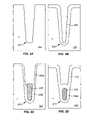
- FIG. 1is a simplified cross section view of a conventional shielded gate trench MOSFET.
- Trench 110includes a shield electrode 114 directly below a gate electrode 122 .
- Shield electrode 114is insulated from adjacent silicon regions by a shield dielectric 112 which is generally thicker than gate dielectric 120 .
- the gate and shield electrodesare insulated from one another by a dielectric layer 116 commonly referred to as inter-poly dielectric or IPD.
- the IPD layermust be of sufficient quality and thickness to support the required voltage between the gate and shield electrodes.
- the conventional shielded gate FET of FIG. 1suffers from a number of drawbacks.
- gate electrode 122has sharp bottom corners which together with the flat top surface of shield electrode 114 leads to high electric fields in these regions.
- conventional methods for forming the IPDtypically introduce an oxide layer on the mesas between trenches that must be removed at some point after the gate electrode has been formed. In removing this oxide some etching of the gate oxide down the trench sidewalls inevitably occurs, which may result in gate shorts and gate leakage.
- Other known techniquestie formation of the IPD to formation of the gate dielectric and thus the IPD thickness is limited to a set multiple of the gate dielectric thickness. This does not allow independent optimization of the gate dielectric and the IPD.
- the largest differential in thickness between the IPD and the gate dielectric achievedhas been about three to one (i.e., for a given target gate dielectric thickness, the largest IPD thickness that has been achieved is about three times greater than that of the target gate dielectric thickness).
- a FETincludes a trench extending into a silicon region of a first conductivity type.
- a shield electrode insulated from the silicon region by a shield dielectricextends in a lower portion of the trench.
- a gate electrodeis in the trench over, but insulated from, the shield electrode by an inter-poly dielectric (IPD).
- the IPDcomprises a conformal layer of dielectric and a thermal oxide layer.
- the gate electrodeis insulated from the silicon region by a gate dielectric extending along upper trench sidewalls, and a ratio of a thickness of the IPD to a thickness of the gate dielectric is greater than three to one.
- the IPDhas a concave profile along its upper surface.
- the gate electrodehas a concave profile along its lower surface.
- the conformal layer of dielectricis surrounded by the thermal dielectric along its lower surface and sidewalls.
- the conformal layer of dielectrichas a convex lower surface and a concave upper surface.
- the shield electrodehas a rounded top surface.
- the silicon regionincludes an epitaxial layer of the first conductivity type extending over a substrate of the first conductivity type, well regions of a second conductivity type in the epitaxial layer, and source regions of the first conductivity in the well regions.
- the source regionsflank the trench.
- the trenchextends into and terminates within the epitaxial layer.
- the trenchextends through the epitaxial layer and terminates within the substrate.
- FIG. 1is a simplified cross section view of a conventional shielded gate trench MOSFET
- FIGS. 2A–2Lare simplified cross section views at various stages of an exemplary process sequence for forming a shielded gate trench FET with improved inter-poly dielectric and gate dielectric, in accordance with an embodiment of the invention.
- an IPD layer of a shielded gate FETis formed by performing a thermal oxidation followed by deposition of a conformal layer of dielectric.
- a gate dielectricis then formed, followed by formation of the gate electrode.
- This methoddecouples the process for forming the IPD layer from that for forming the gate dielectric, enabling each of these dielectric layers to be independently optimized.
- a high quality, thick IPDcan thus be formed to support the required voltage between the gate and shield electrodes without compromising the gate dielectric quality or thickness.
- the conformal layer of dielectrichelps obtain a smooth concave profile (i.e., like the inside of a bowl) along the top surface of the IPD which in turn results in a smooth bottom profile for the gate electrode. This helps reduce the electric field as compared to the conventional FET structure in FIG. 1 where the gate electrode has sharp lower corners.
- FIGS. 2A–2Lare simplified cross section views at various stages of an exemplary process sequence for forming a shielded gate trench FET with improved IPD and gate dielectric, in accordance with an embodiment of the invention.
- a trench 202is formed in silicon region 204 using conventional masking and silicon etch techniques.
- silicon region 204comprises a relatively lightly doped n-type epitaxial layer extending over a highly conductive n-type substrate.
- the trenchcan be etched to terminate within the epitaxial layer or extend deeper to terminate within the substrate.
- a shield dielectric layer 206(e.g., comprising oxide) lining the trench sidewalls and bottom as well as the surface of the mesa regions adjacent the trench is formed using known techniques.
- the shield oxideis formed using high temperature (e.g., 1,150° C.) dry oxidation. The high temperature helps round out the trench bottom corners and form about 1,250 ⁇ of shield oxide sufficient to support device breakdown.
- a layer of polysiliconis deposited to fill the trench using conventional polysilicon deposition techniques.
- the deposited polysiliconis then recessed into the trench to thereby form shield electrode 208 .
- the exposed portions of the shield dielectric layerare then thinned down, to for example 650 ⁇ .
- a wet buffered oxide etchis used to thin down the shield oxide.
- the remaining exposed portion 206 a of the shield dielectrichelps prevent excessive growth of oxide along the trench sidewalls and mesa surfaces in the subsequent thermal oxidation step, and helps control the profile of the trenched cavity. Excessive growth of thermal oxide can lead to formation of voids in the subsequent deposited conformal dielectric.
- the exposed portions of shield dielectric 206are completely removed or alternatively the entire shield dielectric 206 is left intact.
- a thermal oxidation stepis carried out to form a thermal oxide layer 210 along the trench sidewalls, over the surface of the mesa regions adjacent the trench, and over shield electrode 208 .
- the thermal oxidationadvantageously oxidizes an upper portion of shield electrode 208 resulting in a rounded-top profile. The rounded top helps minimize electric field in the regions between shield electrode 208 and the gate electrode formed later.
- thermal oxide layer 210is formed by performing a low temperature, wet oxidation followed by a high temperature, dry oxidation.
- the thermal oxidationyields a thermal oxide layer 210 with a thickness in the range of 1000–1500 ⁇ .
- a low temperature thermal oxidation(e.g., about 850° C.) is carried out so that a thicker thermal oxide layer is formed along the top surface of the shield electrode than along the trench sidewalls and over the mesa surfaces.
- a thickness ratio in the range of 1.5:1 to 2:1would be desirable.
- the thermal oxidationyields a thermal oxide layer having a thickness of about 1,850 ⁇ along the top surface of the shield electrode and a thickness of about 1,250 ⁇ along the trench sidewalls and the mesa surfaces.
- a conformal layer of dielectric 212(e.g., comprising oxide) is deposited to fill the trench.
- conformal dielectric layer 212is deposited using a sub-atmospheric chemical vapor deposition (SACVD) tetraethylorthosilicate (TEOS)/Ozone process at a temperature of about 510° C. and pressure of about 480 Torr. The deposited oxide fills the trench completely without voiding.
- SACVDsub-atmospheric chemical vapor deposition
- TEOStetraethylorthosilicate
- IPD layer 214thus comprises a stack of thermal dielectric layer and conformal dielectric layer.
- a uniform etch back of the dielectric stackis carried out in recessing the dielectric stack into the trench.
- a dry anisotropic plasma etch or a wet etchcan be carried out to achieve the desired thickness for the IPD and to ensure that the oxide along the trench sidewalls and over the mesa is completely removed.
- a conventional densification stepcan also be carried out to densify the SACVD oxide. In one embodiment, a dry etch and a subsequent densification are carried out, followed by a wet etch.
- a gate dielectric layer 216(e.g., from oxide) extending along trench sidewalls, over the IPD layer, and over the mesa regions adjacent the trench is formed using conventional techniques. Because the IPD formation is completely decoupled from the gate dielectric formation, the gate dielectric can be independently optimized to have the desired characteristics.
- a layer of polysiliconis deposited to fill the trench, and is then etched back to form a recessed gate electrode 218 in trench 202 .
- the portion of gate dielectric 216 extending over the mesais etched back to a thickness suitable for body implant and source implant.
- a conventional blanket body implant and drive in processis performed to form p-type body regions 220 along an upper portion of silicon region 204 .
- a conventional source implant together with a masking layer (not shown)is then used to form source regions 222 flanking trench 202 .
- a pre-metal dielectric layer 224(e.g., comprising BPSG) is formed over the structure using conventional techniques.
- dielectric layer 224is partially removed to expose surfaces of body regions 220 and source regions 222 as defined by the masking layer.
- a conventional silicon etche.g., dry etch
- the recessed silicon regionsthus form contact openings 226 .
- a blanket heavy body implantis carried out to form self-aligned p-type heavy body regions 228 in body regions 220 .
- a reflow of dielectric 224is then carried out to obtain a better aspect ratio for the contact openings and a better step coverage for a metal layer 226 which is formed in a subsequent step to electrically contact heavy body regions 228 and source regions 222 .
- a horizontally extending dashed lineis included in FIG. 2L to illustrate the embodiment wherein an epitaxial layer 203 extends over a substrate 201 , and trench 202 extends through epitaxial layer 203 and terminates in substrate 201 . Alternatively, trench 202 may be terminated within epitaxial layer 203 .
- FIGS. 2A–2Lthe process sequence depicted by cross section views in FIGS. 2A–2L is merely exemplary and the various steps can be modified or carried out in a different sequence than that shown.
- any one of a number of known process stepscan be carried out instead of those depicted by FIGS. 2I–2L to obtain a shielded gate structure with the desired features and characteristics.
- an improved IPD layercomprising a film stack of a thermally grown dielectric and a conformal deposited dielectric is obtained.
- the thermally grown dielectricprovides a high quality dielectric and serves to round off the top corners of the shield electrode.
- the conformal deposited dielectric(1) fills in the gaps on the upper side of the shield electrode, (2) serves as a hard mask to protect the thermal dielectric over the shield electrode while the dielectric along the trench sidewalls is being etched, and (3) creates a smooth concave profile over which the gate electrode is formed.
- the rounded profile along the top surface of the shield electrode and the bottom of the gate electroderesult in lower electric fields in these localized areas.
- the method of forming the IPD in accordance with the inventionserves to decouple formation of the IPD from that of the gate oxide so that the IPD and gate dielectric can be independently optimized to, for example, achieve a thick, high quality IPD and a thin, high quality gate dielectric.
- optimum transistor characteristicsare obtained by using a ratio of IPD thickness to gate dielectric thickness of greater than about five to one. For example, an IPD thickness of greater than about 2,000 ⁇ , and a gate dielectric thickness of less than about 400 ⁇ is found to provide optimum transistor characteristics.
- the ability to form a thin gate dielectriccan advantageously be used to achieve a lower on resistance.
- FIGS. 2A–2LThe process sequence depicted by FIGS. 2A–2L is for forming an n-channel FET, however modifying this process sequence to form a p-channel FET would be obvious to one skilled in the art in view of this disclosure.
- the various embodiments described aboveare implemented in conventional silicon, these embodiments and their obvious variants can also be implemented in silicon carbide, gallium arsenide, gallium nitride, diamond or other semiconductor materials.
- the cross-section views of the different embodimentsmay not be to scale, and as such are not intended to limit the possible variations in the layout design of the corresponding structures.
- the FET shown and its obvious variantscan be formed in stripe or cellular architecture including hexagonal or square shaped transistor cells.
- the features of one or more embodiments of the inventionmay be combined with one or more features of other embodiments of the invention without departing from the scope of the invention. Hence, the scope of this invention should not be limited to the embodiments described, but are instead defined by the following claims.
Landscapes
- Insulated Gate Type Field-Effect Transistor (AREA)
- Electrodes Of Semiconductors (AREA)
Abstract
Description
Claims (21)
Priority Applications (11)
| Application Number | Priority Date | Filing Date | Title |
|---|---|---|---|
| US11/201,400US7385248B2 (en) | 2005-08-09 | 2005-08-09 | Shielded gate field effect transistor with improved inter-poly dielectric |
| AT0934506AAT504736A2 (en) | 2005-08-09 | 2006-08-04 | STRUCTURE AND METHOD FOR FORMING AN INTER POLY DIELECTRIC SYSTEM IN A FIELD EFFECT TRANSISTOR WITH SHIELDED GATE |
| CN2006800287698ACN101238581B (en) | 2005-08-09 | 2006-08-04 | Structure and method for forming inter-poly dielectric in shielded gate field effect transistor |
| JP2008526148AJP5075823B2 (en) | 2005-08-09 | 2006-08-04 | Structure and manufacturing method of interpoly insulating film in shield gate field effect transistor. |
| CN2010101186508ACN101800245B (en) | 2005-08-09 | 2006-08-04 | Structure and method for forming inter-poly dielectric in a shielded gate field effect transistor |
| KR1020087005785AKR101221242B1 (en) | 2005-08-09 | 2006-08-04 | Structure and method for forming inter-poly dielectric in a shielded gate field effect transistor |
| PCT/US2006/030944WO2007021701A2 (en) | 2005-08-09 | 2006-08-04 | Structure and method for forming inter-poly dielectric in a shielded gate field effect transistor |
| DE112006002077.3TDE112006002077B4 (en) | 2005-08-09 | 2006-08-04 | Method of forming an inter-poly dielectric field effect transistor and shielded gate field effect transistor |
| MYPI20063822AMY141412A (en) | 2005-08-09 | 2006-08-08 | Shielded gate field effect transistor with improved inter-poly dielectric |
| TW095129026ATWI417963B (en) | 2005-08-09 | 2006-08-08 | Structure and method for forming interelectrode dielectric in shielding gate field effect transistor |
| US11/952,481US7598144B2 (en) | 2005-08-09 | 2007-12-07 | Method for forming inter-poly dielectric in shielded gate field effect transistor |
Applications Claiming Priority (1)
| Application Number | Priority Date | Filing Date | Title |
|---|---|---|---|
| US11/201,400US7385248B2 (en) | 2005-08-09 | 2005-08-09 | Shielded gate field effect transistor with improved inter-poly dielectric |
Related Child Applications (1)
| Application Number | Title | Priority Date | Filing Date |
|---|---|---|---|
| US11/952,481DivisionUS7598144B2 (en) | 2005-08-09 | 2007-12-07 | Method for forming inter-poly dielectric in shielded gate field effect transistor |
Publications (2)
| Publication Number | Publication Date |
|---|---|
| US20070037327A1 US20070037327A1 (en) | 2007-02-15 |
| US7385248B2true US7385248B2 (en) | 2008-06-10 |
Family
ID=37743042
Family Applications (2)
| Application Number | Title | Priority Date | Filing Date |
|---|---|---|---|
| US11/201,400Expired - LifetimeUS7385248B2 (en) | 2005-08-09 | 2005-08-09 | Shielded gate field effect transistor with improved inter-poly dielectric |
| US11/952,481Active2025-12-03US7598144B2 (en) | 2005-08-09 | 2007-12-07 | Method for forming inter-poly dielectric in shielded gate field effect transistor |
Family Applications After (1)
| Application Number | Title | Priority Date | Filing Date |
|---|---|---|---|
| US11/952,481Active2025-12-03US7598144B2 (en) | 2005-08-09 | 2007-12-07 | Method for forming inter-poly dielectric in shielded gate field effect transistor |
Country Status (9)
| Country | Link |
|---|---|
| US (2) | US7385248B2 (en) |
| JP (1) | JP5075823B2 (en) |
| KR (1) | KR101221242B1 (en) |
| CN (2) | CN101238581B (en) |
| AT (1) | AT504736A2 (en) |
| DE (1) | DE112006002077B4 (en) |
| MY (1) | MY141412A (en) |
| TW (1) | TWI417963B (en) |
| WO (1) | WO2007021701A2 (en) |
Cited By (41)
| Publication number | Priority date | Publication date | Assignee | Title |
|---|---|---|---|---|
| US20090206395A1 (en)* | 2008-02-20 | 2009-08-20 | Force-Mos Technology Corporation | Trench mosfet with double epitaxial structure |
| US20090206401A1 (en)* | 2005-08-31 | 2009-08-20 | Infineon Technologies Ag | Trench transistor and method for fabricating a trench transistor |
| US20090230467A1 (en)* | 2005-05-20 | 2009-09-17 | Yoshito Nakazawa | Semiconductor device and manufacturing method of the same |
| US7598144B2 (en) | 2005-08-09 | 2009-10-06 | Fairchild Semiconductor Corporation | Method for forming inter-poly dielectric in shielded gate field effect transistor |
| US20100006928A1 (en)* | 2008-07-09 | 2010-01-14 | James Pan | Structure and Method for Forming a Shielded Gate Trench FET with an Inter-electrode Dielectric Having a Low-k Dielectric Therein |
| US20100117144A1 (en)* | 2008-11-10 | 2010-05-13 | Infineon Technologies Austria Ag | Semiconductor device and method for the production of a semiconductor device |
| US20100200910A1 (en)* | 2009-02-09 | 2010-08-12 | Joseph Yedinak | Semiconductor Devices with Stable and Controlled Avalanche Characteristics and Methods of Fabricating the Same |
| US20100207205A1 (en)* | 2009-02-19 | 2010-08-19 | Grebs Thomas E | Structures and Methods for Improving Trench-Shielded Semiconductor Devices and Schottky Barrier Rectifier Devices |
| US20100308400A1 (en)* | 2008-06-20 | 2010-12-09 | Maxpower Semiconductor Inc. | Semiconductor Power Switches Having Trench Gates |
| US20100314707A1 (en)* | 2009-06-12 | 2010-12-16 | Yedinak Joseph A | Reduced Process Sensitivity of Electrode-Semiconductor Rectifiers |
| US20110089485A1 (en)* | 2009-10-21 | 2011-04-21 | Vishay-Siliconix | Split gate semiconductor device with curved gate oxide profile |
| US20110136310A1 (en)* | 2009-12-09 | 2011-06-09 | Grivna Gordon M | Method of forming an insulated gate field effect transistor device having a shield electrode structure |
| US20110147836A1 (en)* | 2008-08-20 | 2011-06-23 | Hebert Francois | Charged balanced devices with shielded gate trench |
| US8174067B2 (en) | 2008-12-08 | 2012-05-08 | Fairchild Semiconductor Corporation | Trench-based power semiconductor devices with increased breakdown voltage characteristics |
| US8304829B2 (en) | 2008-12-08 | 2012-11-06 | Fairchild Semiconductor Corporation | Trench-based power semiconductor devices with increased breakdown voltage characteristics |
| US20120292693A1 (en)* | 2009-08-31 | 2012-11-22 | Alpha & Omega Semiconductor Incorporated | Fabrication of trench dmos device having thick bottom shielding oxide |
| US20130009240A1 (en)* | 2004-08-04 | 2013-01-10 | Rohm Co., Ltd. | Semiconductor device and method for manufacturing the same |
| US8927369B2 (en) | 2012-07-13 | 2015-01-06 | Ubiq Semiconductor Corp. | Method of forming a trench gate MOSFET having a thick bottom oxide |
| US20150008515A1 (en)* | 2012-07-13 | 2015-01-08 | Ubiq Semiconductor Corp. | Trench gate mosfet |
| US9425305B2 (en) | 2009-10-20 | 2016-08-23 | Vishay-Siliconix | Structures of and methods of fabricating split gate MIS devices |
| CN105895516A (en)* | 2016-04-29 | 2016-08-24 | 深圳尚阳通科技有限公司 | Method for manufacturing trench gate MOSFET with shielding grid |
| US9577089B2 (en) | 2010-03-02 | 2017-02-21 | Vishay-Siliconix | Structures and methods of fabricating dual gate devices |
| US9653560B1 (en) | 2016-05-18 | 2017-05-16 | Excellence MOS Corporation | Method of fabricating power MOSFET |
| US9825137B2 (en) | 2013-09-12 | 2017-11-21 | Magnachip Semiconductor, Ltd. | Semiconductor element and method for producing the same |
| US9941357B2 (en) | 2016-05-18 | 2018-04-10 | Excelliance Mos Corporation | Power MOSFET |
| US9947751B2 (en) | 2016-09-16 | 2018-04-17 | Kabushiki Kaisha Toshiba | Semiconductor device and method of manufacturing the same |
| US10153357B1 (en) | 2017-08-28 | 2018-12-11 | Nxp Usa, Inc. | Superjunction power semiconductor device and method for forming |
| US10234486B2 (en) | 2014-08-19 | 2019-03-19 | Vishay/Siliconix | Vertical sense devices in vertical trench MOSFET |
| US10388737B2 (en) | 2016-05-23 | 2019-08-20 | General Electric Company | Electric field shielding in silicon carbide metal-oxide-semiconductor (MOS) devices having an optimization layer |
| US20190304787A1 (en)* | 2016-02-01 | 2019-10-03 | Fuji Electric Co., Ltd. | Method of manufacturing silicon carbide semiconductor device |
| US10468519B2 (en) | 2017-04-26 | 2019-11-05 | National Tsing Hua University | Structure of trench metal-oxide-semiconductor field-effect transistor |
| US10811502B1 (en) | 2019-05-30 | 2020-10-20 | Nxp Usa, Inc. | Method of manufacture of super-junction power semiconductor device |
| US10847646B2 (en) | 2018-09-14 | 2020-11-24 | Kabushiki Kaisha Toshiba | Semiconductor device |
| US11114559B2 (en) | 2011-05-18 | 2021-09-07 | Vishay-Siliconix, LLC | Semiconductor device having reduced gate charges and superior figure of merit |
| US11218144B2 (en) | 2019-09-12 | 2022-01-04 | Vishay-Siliconix, LLC | Semiconductor device with multiple independent gates |
| US11217541B2 (en) | 2019-05-08 | 2022-01-04 | Vishay-Siliconix, LLC | Transistors with electrically active chip seal ring and methods of manufacture |
| US20220254908A1 (en)* | 2021-02-05 | 2022-08-11 | Mitsubishi Electric Corporation | Semiconductor device and a manufacturing method of semiconductor device |
| EP4057359A1 (en) | 2021-03-08 | 2022-09-14 | Nexperia B.V. | Semiconductor device comprising mutually separated trench structures |
| US20230420529A1 (en)* | 2022-06-26 | 2023-12-28 | Vanguard International Semiconductor Corporation | Semiconductor device and fabrication method thereof |
| US11862695B2 (en) | 2021-05-31 | 2024-01-02 | Key Foundry Co., Ltd. | Split gate power MOSFET and split gate power MOSFET manufacturing method |
| WO2025137902A1 (en)* | 2023-12-27 | 2025-07-03 | Nexperia Technology (Shanghai) Ltd. | Semiconductor device and method for providing electrode in semiconductor device |
Families Citing this family (59)
| Publication number | Priority date | Publication date | Assignee | Title |
|---|---|---|---|---|
| US6838722B2 (en) | 2002-03-22 | 2005-01-04 | Siliconix Incorporated | Structures of and methods of fabricating trench-gated MIS devices |
| KR100550351B1 (en)* | 2004-09-07 | 2006-02-08 | 삼성전자주식회사 | A film forming method of a semiconductor device and a film forming device of a semiconductor device for performing the same |
| US7319256B1 (en)* | 2006-06-19 | 2008-01-15 | Fairchild Semiconductor Corporation | Shielded gate trench FET with the shield and gate electrodes being connected together |
| US20080272429A1 (en)* | 2007-05-04 | 2008-11-06 | Icemos Technology Corporation | Superjunction devices having narrow surface layout of terminal structures and methods of manufacturing the devices |
| US20090242973A1 (en)* | 2008-03-31 | 2009-10-01 | Alpha & Omega Semiconductor, Ltd. | Source and body contact structure for trench-dmos devices using polysilicon |
| US8174071B2 (en)* | 2008-05-02 | 2012-05-08 | Taiwan Semiconductor Manufacturing Co., Ltd. | High voltage LDMOS transistor |
| WO2010010543A1 (en)* | 2008-07-25 | 2010-01-28 | Nxp B.V. | A trench-gate semiconductor device |
| US8278702B2 (en)* | 2008-09-16 | 2012-10-02 | Fairchild Semiconductor Corporation | High density trench field effect transistor |
| US20100187602A1 (en)* | 2009-01-29 | 2010-07-29 | Woolsey Debra S | Methods for making semiconductor devices using nitride consumption locos oxidation |
| US8143125B2 (en)* | 2009-03-27 | 2012-03-27 | Fairchild Semiconductor Corporation | Structure and method for forming a salicide on the gate electrode of a trench-gate FET |
| US8072027B2 (en)* | 2009-06-08 | 2011-12-06 | Fairchild Semiconductor Corporation | 3D channel architecture for semiconductor devices |
| US8072028B2 (en)* | 2009-10-26 | 2011-12-06 | Infineon Technologies Austria Ag | Method and device including transistor component having a field electrode |
| US9306056B2 (en) | 2009-10-30 | 2016-04-05 | Vishay-Siliconix | Semiconductor device with trench-like feed-throughs |
| US8021947B2 (en)* | 2009-12-09 | 2011-09-20 | Semiconductor Components Industries, Llc | Method of forming an insulated gate field effect transistor device having a shield electrode structure |
| US8580667B2 (en) | 2010-12-14 | 2013-11-12 | Alpha And Omega Semiconductor Incorporated | Self aligned trench MOSFET with integrated diode |
| CN102623501B (en)* | 2011-01-28 | 2015-06-03 | 万国半导体股份有限公司 | Shielded gate trench MOSFET with increased source-metal contact |
| US8610205B2 (en) | 2011-03-16 | 2013-12-17 | Fairchild Semiconductor Corporation | Inter-poly dielectric in a shielded gate MOSFET device |
| US8680607B2 (en)* | 2011-06-20 | 2014-03-25 | Maxpower Semiconductor, Inc. | Trench gated power device with multiple trench width and its fabrication process |
| US20130001678A1 (en)* | 2011-06-29 | 2013-01-03 | Stmicroelectronics S.R.L. | High breakdown voltage semiconductor device with an insulated gate formed in a trench, and manufacturing process thereof |
| US8872278B2 (en) | 2011-10-25 | 2014-10-28 | Fairchild Semiconductor Corporation | Integrated gate runner and field implant termination for trench devices |
| US8816431B2 (en)* | 2012-03-09 | 2014-08-26 | Fairchild Semiconductor Corporation | Shielded gate MOSFET device with a funnel-shaped trench |
| CN103367144A (en)* | 2012-03-26 | 2013-10-23 | 马克斯半导体股份有限公司 | Trench-type structure of junction electric-field shielding power MOSFET and manufacturing method |
| KR101893615B1 (en)* | 2012-06-15 | 2018-08-31 | 매그나칩 반도체 유한회사 | Semiconductor Device and Fabricating Method Thereof |
| CN103632950B (en)* | 2012-08-20 | 2016-02-10 | 上海华虹宏力半导体制造有限公司 | Nitride film formation method between polysilicon in groove type double-layer grid MOS |
| CN103632949B (en)* | 2012-08-28 | 2016-06-08 | 上海华虹宏力半导体制造有限公司 | The forming method of the hot oxygen medium layer of the inter polysilicon of groove type double-layer grid MOS |
| JP5811973B2 (en) | 2012-09-12 | 2015-11-11 | 住友電気工業株式会社 | Method for manufacturing silicon carbide semiconductor device |
| JP6056292B2 (en) | 2012-09-12 | 2017-01-11 | 住友電気工業株式会社 | Method for manufacturing silicon carbide semiconductor device |
| JP2014056913A (en) | 2012-09-12 | 2014-03-27 | Sumitomo Electric Ind Ltd | Silicon carbide semiconductor device |
| US9000497B2 (en)* | 2012-09-14 | 2015-04-07 | Renesas Electronics Corporation | Trench MOSFET having an independent coupled element in a trench |
| CN103855017B (en)* | 2012-12-03 | 2016-08-17 | 上海华虹宏力半导体制造有限公司 | The method forming groove type double-layer grid MOS structure two-layer polysilicon lateral isolation |
| EP3005419A4 (en)* | 2013-06-06 | 2017-03-15 | United Silicon Carbide Inc. | Trench shield connected jfet |
| TWI528424B (en)* | 2013-08-05 | 2016-04-01 | 台灣茂矽電子股份有限公司 | Method for forming shielding gate in gold oxide half field effect transistor |
| KR102156130B1 (en) | 2014-04-10 | 2020-09-15 | 삼성전자주식회사 | Method of Forming Semiconductor device |
| US9257622B2 (en)* | 2014-04-14 | 2016-02-09 | Jin-Ywan Lin | Light-emitting structure |
| CN105789043B (en)* | 2014-12-25 | 2019-03-12 | 华润微电子(重庆)有限公司 | Trench type semiconductor device and method of making the same |
| US10396215B2 (en) | 2015-03-10 | 2019-08-27 | United Silicon Carbide, Inc. | Trench vertical JFET with improved threshold voltage control |
| JP6519894B2 (en)* | 2016-03-31 | 2019-05-29 | 新電元工業株式会社 | Semiconductor device manufacturing method and semiconductor device |
| TWI643253B (en)* | 2016-05-18 | 2018-12-01 | 杰力科技股份有限公司 | Method of fabricating power mosfet |
| CN109216449B (en)* | 2017-06-30 | 2021-07-30 | 帅群微电子股份有限公司 | Trench type power semiconductor device and method of manufacturing the same |
| CN107871787B (en)* | 2017-10-11 | 2021-10-12 | 矽力杰半导体技术(杭州)有限公司 | Method for manufacturing trench MOSFET |
| TW201926470A (en)* | 2017-12-06 | 2019-07-01 | 力祥半導體股份有限公司 | Trench gate MOSFET |
| CN108389800A (en)* | 2018-01-31 | 2018-08-10 | 华润微电子(重庆)有限公司 | The manufacturing method of shield grid trench FET |
| US10714574B2 (en)* | 2018-05-08 | 2020-07-14 | Ipower Semiconductor | Shielded trench devices |
| JP7061954B2 (en)* | 2018-11-07 | 2022-05-02 | 三菱電機株式会社 | Semiconductor device |
| CN111613674B (en)* | 2019-02-25 | 2024-10-25 | 恒泰柯半导体(上海)有限公司 | Deep Trench MOSFET |
| CN111863617A (en)* | 2019-04-24 | 2020-10-30 | 帅群微电子股份有限公司 | Trench type power semiconductor component and method of making the same |
| CN110335895A (en)* | 2019-07-31 | 2019-10-15 | 上海昱率科技有限公司 | Power device and manufacturing method thereof |
| CN110896026A (en)* | 2019-11-22 | 2020-03-20 | 矽力杰半导体技术(杭州)有限公司 | Trench type MOSFET structure and manufacturing method thereof |
| CN112864018B (en)* | 2019-11-28 | 2022-07-19 | 华润微电子(重庆)有限公司 | Trench type field effect transistor structure and preparation method thereof |
| EP3859788A1 (en)* | 2020-01-29 | 2021-08-04 | Infineon Technologies Austria AG | Transistor device and method of forming a field plate in an elongate active trench of a transistor device |
| CN111276394B (en)* | 2020-02-18 | 2022-09-23 | 捷捷微电(上海)科技有限公司 | A kind of manufacturing method of split gate MOSFET |
| DE102020205706A1 (en) | 2020-05-06 | 2021-11-11 | Robert Bosch Gesellschaft mit beschränkter Haftung | Method of making a low-defect junction |
| CN113327858B (en)* | 2020-07-15 | 2024-02-06 | 上海积塔半导体有限公司 | Shielded gate field effect transistor and method of manufacturing the same |
| CN111681963B (en)* | 2020-08-11 | 2020-11-20 | 中芯集成电路制造(绍兴)有限公司 | Shielded gate field effect transistor and method of forming the same |
| US11848378B2 (en)* | 2020-08-13 | 2023-12-19 | Stmicroelectronics Pte Ltd | Split-gate trench power MOSFET with self-aligned poly-to-poly isolation |
| CN114582717A (en)* | 2020-11-30 | 2022-06-03 | 无锡华润上华科技有限公司 | Preparation method of semiconductor device and shielded gate trench device |
| JP7572928B2 (en) | 2021-09-16 | 2024-10-24 | ウィル セミコンダクター (シャンハイ) カンパニー リミテッド | Field effect transistor and method for manufacturing the same |
| CN114678275B (en)* | 2021-12-29 | 2024-07-30 | 杭州芯迈半导体技术有限公司 | Split-gate MOSFET and method of manufacturing the same |
| CN114242578B (en)* | 2022-02-21 | 2022-06-17 | 威海银创微电子技术有限公司 | Controllable method, device and medium for IPO thickness in SGT Mosfet |
Citations (325)
| Publication number | Priority date | Publication date | Assignee | Title |
|---|---|---|---|---|
| US3404295A (en) | 1964-11-30 | 1968-10-01 | Motorola Inc | High frequency and voltage transistor with added region for punch-through protection |
| US3412297A (en) | 1965-12-16 | 1968-11-19 | United Aircraft Corp | Mos field-effect transistor with a onemicron vertical channel |
| US3497777A (en) | 1967-06-13 | 1970-02-24 | Stanislas Teszner | Multichannel field-effect semi-conductor device |
| US3564356A (en) | 1968-10-24 | 1971-02-16 | Tektronix Inc | High voltage integrated circuit transistor |
| US3660697A (en) | 1970-02-16 | 1972-05-02 | Bell Telephone Labor Inc | Monolithic semiconductor apparatus adapted for sequential charge transfer |
| US4003072A (en) | 1972-04-20 | 1977-01-11 | Sony Corporation | Semiconductor device with high voltage breakdown resistance |
| US4011105A (en) | 1975-09-15 | 1977-03-08 | Mos Technology, Inc. | Field inversion control for n-channel device integrated circuits |
| JPS5658267A (en) | 1979-10-17 | 1981-05-21 | Nippon Telegr & Teleph Corp <Ntt> | Insulated gate type field-effect transistor |
| US4300150A (en) | 1980-06-16 | 1981-11-10 | North American Philips Corporation | Lateral double-diffused MOS transistor device |
| US4324038A (en) | 1980-11-24 | 1982-04-13 | Bell Telephone Laboratories, Incorporated | Method of fabricating MOS field effect transistors |
| US4326332A (en) | 1980-07-28 | 1982-04-27 | International Business Machines Corp. | Method of making a high density V-MOS memory array |
| US4337474A (en) | 1978-08-31 | 1982-06-29 | Mitsubishi Denki Kabushiki Kaisha | Semiconductor device |
| US4345265A (en) | 1980-04-14 | 1982-08-17 | Supertex, Inc. | MOS Power transistor with improved high-voltage capability |
| US4445202A (en) | 1980-11-12 | 1984-04-24 | International Business Machines Corporation | Electrically switchable permanent storage |
| US4568958A (en) | 1984-01-03 | 1986-02-04 | General Electric Company | Inversion-mode insulated-gate gallium arsenide field-effect transistors |
| US4579621A (en) | 1983-07-08 | 1986-04-01 | Mitsubishi Denki Kabushiki Kaisha | Selective epitaxial growth method |
| US4636281A (en) | 1984-06-14 | 1987-01-13 | Commissariat A L'energie Atomique | Process for the autopositioning of a local field oxide with respect to an insulating trench |
| US4638344A (en) | 1979-10-09 | 1987-01-20 | Cardwell Jr Walter T | Junction field-effect transistor controlled by merged depletion regions |
| US4639761A (en) | 1983-12-16 | 1987-01-27 | North American Philips Corporation | Combined bipolar-field effect transistor resurf devices |
| JPS6269562A (en) | 1985-09-20 | 1987-03-30 | Mitsubishi Electric Corp | Field effect transistor device and method for manufacturing the same |
| US4673962A (en) | 1985-03-21 | 1987-06-16 | Texas Instruments Incorporated | Vertical DRAM cell and method |
| US4698653A (en) | 1979-10-09 | 1987-10-06 | Cardwell Jr Walter T | Semiconductor devices controlled by depletion regions |
| US4716126A (en) | 1986-06-05 | 1987-12-29 | Siliconix Incorporated | Fabrication of double diffused metal oxide semiconductor transistor |
| US4745079A (en) | 1987-03-30 | 1988-05-17 | Motorola, Inc. | Method for fabricating MOS transistors having gates with different work functions |
| US4746630A (en) | 1986-09-17 | 1988-05-24 | Hewlett-Packard Company | Method for producing recessed field oxide with improved sidewall characteristics |
| US4754310A (en) | 1980-12-10 | 1988-06-28 | U.S. Philips Corp. | High voltage semiconductor device |
| US4767722A (en) | 1986-03-24 | 1988-08-30 | Siliconix Incorporated | Method for making planar vertical channel DMOS structures |
| US4774556A (en) | 1985-07-25 | 1988-09-27 | Nippondenso Co., Ltd. | Non-volatile semiconductor memory device |
| JPS63288047A (en) | 1987-05-20 | 1988-11-25 | Toshiba Corp | Semiconductor device and its manufacturing method |
| JPS63186475U (en) | 1987-05-22 | 1988-11-30 | ||
| US4801986A (en) | 1987-04-03 | 1989-01-31 | General Electric Company | Vertical double diffused metal oxide semiconductor VDMOS device with increased safe operating area and method |
| JPS6422051U (en) | 1987-07-30 | 1989-02-03 | ||
| US4821095A (en) | 1987-03-12 | 1989-04-11 | General Electric Company | Insulated gate semiconductor device with extra short grid and method of fabrication |
| US4823176A (en) | 1987-04-03 | 1989-04-18 | General Electric Company | Vertical double diffused metal oxide semiconductor (VDMOS) device including high voltage junction exhibiting increased safe operating area |
| US4824793A (en) | 1984-09-27 | 1989-04-25 | Texas Instruments Incorporated | Method of making DRAM cell with trench capacitor |
| US4853345A (en) | 1988-08-22 | 1989-08-01 | Delco Electronics Corporation | Process for manufacture of a vertical DMOS transistor |
| JPH01192174A (en) | 1988-01-27 | 1989-08-02 | Hitachi Ltd | Manufacturing method of semiconductor device |
| US4868624A (en) | 1980-05-09 | 1989-09-19 | Regents Of The University Of Minnesota | Channel collector transistor |
| US4893160A (en) | 1987-11-13 | 1990-01-09 | Siliconix Incorporated | Method for increasing the performance of trenched devices and the resulting structure |
| US4914058A (en) | 1987-12-29 | 1990-04-03 | Siliconix Incorporated | Grooved DMOS process with varying gate dielectric thickness |
| US4941026A (en) | 1986-12-05 | 1990-07-10 | General Electric Company | Semiconductor devices exhibiting minimum on-resistance |
| US4961100A (en) | 1988-06-20 | 1990-10-02 | General Electric Company | Bidirectional field effect semiconductor device and circuit |
| US4967245A (en) | 1988-03-14 | 1990-10-30 | Siliconix Incorporated | Trench power MOSFET device |
| US4969028A (en) | 1980-12-02 | 1990-11-06 | General Electric Company | Gate enhanced rectifier |
| US4974059A (en) | 1982-12-21 | 1990-11-27 | International Rectifier Corporation | Semiconductor high-power mosfet device |
| US4975782A (en) | 1988-02-22 | 1990-12-04 | Asea Brown Boveri Ltd. | Field effect controlled, bipolar power semiconductor component with silicide layer |
| US4990463A (en) | 1988-07-05 | 1991-02-05 | Kabushiki Kaisha Toshiba | Method of manufacturing capacitor |
| US4992390A (en) | 1989-07-06 | 1991-02-12 | General Electric Company | Trench gate structure with thick bottom oxide |
| US5027180A (en) | 1986-12-11 | 1991-06-25 | Mitsubishi Electric Corporation | Double gate static induction thyristor |
| US5034785A (en) | 1986-03-24 | 1991-07-23 | Siliconix Incorporated | Planar vertical channel DMOS structure |
| US5065273A (en) | 1990-12-04 | 1991-11-12 | International Business Machines Corporation | High capacity DRAM trench capacitor and methods of fabricating same |
| US5072266A (en) | 1988-12-27 | 1991-12-10 | Siliconix Incorporated | Trench DMOS power transistor with field-shaping body profile and three-dimensional geometry |
| US5071782A (en) | 1990-06-28 | 1991-12-10 | Texas Instruments Incorporated | Vertical memory cell array and method of fabrication |
| US5079608A (en) | 1990-11-06 | 1992-01-07 | Harris Corporation | Power MOSFET transistor circuit with active clamp |
| US5105243A (en) | 1987-02-26 | 1992-04-14 | Kabushiki Kaisha Toshiba | Conductivity-modulation metal oxide field effect transistor with single gate structure |
| US5111253A (en) | 1989-05-09 | 1992-05-05 | General Electric Company | Multicellular FET having a Schottky diode merged therewith |
| US5134448A (en) | 1990-01-29 | 1992-07-28 | Motorola, Inc. | MOSFET with substrate source contact |
| US5142640A (en) | 1988-06-02 | 1992-08-25 | Seiko Epson Corporation | Trench gate metal oxide semiconductor field effect transistor |
| US5156989A (en) | 1988-11-08 | 1992-10-20 | Siliconix, Incorporated | Complementary, isolated DMOS IC technology |
| US5164802A (en) | 1991-03-20 | 1992-11-17 | Harris Corporation | Power vdmosfet with schottky on lightly doped drain of lateral driver fet |
| US5164325A (en) | 1987-10-08 | 1992-11-17 | Siliconix Incorporated | Method of making a vertical current flow field effect transistor |
| US5168331A (en) | 1991-01-31 | 1992-12-01 | Siliconix Incorporated | Power metal-oxide-semiconductor field effect transistor |
| US5168973A (en) | 1987-03-25 | 1992-12-08 | Kabushiki Kaisha Komatsu Seisakusho | Apparatus for controlling hydraulic pressure for clutch |
| US5188973A (en) | 1991-05-09 | 1993-02-23 | Nippon Telegraph & Telephone Corporation | Method of manufacturing SOI semiconductor element |
| US5208657A (en) | 1984-08-31 | 1993-05-04 | Texas Instruments Incorporated | DRAM Cell with trench capacitor and vertical channel in substrate |
| US5216275A (en) | 1991-03-19 | 1993-06-01 | University Of Electronic Science And Technology Of China | Semiconductor power devices with alternating conductivity type high-voltage breakdown regions |
| US5219777A (en) | 1991-06-14 | 1993-06-15 | Gold Star Electron Co., Ltd. | Metal oxide semiconductor field effect transistor and method of making the same |
| US5219793A (en) | 1991-06-03 | 1993-06-15 | Motorola Inc. | Method for forming pitch independent contacts and a semiconductor device having the same |
| US5233215A (en) | 1992-06-08 | 1993-08-03 | North Carolina State University At Raleigh | Silicon carbide power MOSFET with floating field ring and floating field plate |
| JPH05226638A (en) | 1992-02-07 | 1993-09-03 | Shindengen Electric Mfg Co Ltd | Semiconductor device |
| US5242845A (en) | 1990-06-13 | 1993-09-07 | Kabushiki Kaisha Toshiba | Method of production of vertical MOS transistor |
| US5250450A (en) | 1991-04-08 | 1993-10-05 | Micron Technology, Inc. | Insulated-gate vertical field-effect transistor with high current drive and minimum overlap capacitance |
| US5262336A (en) | 1986-03-21 | 1993-11-16 | Advanced Power Technology, Inc. | IGBT process to produce platinum lifetime control |
| US5268311A (en) | 1988-09-01 | 1993-12-07 | International Business Machines Corporation | Method for forming a thin dielectric layer on a substrate |
| DE4300806C1 (en) | 1993-01-14 | 1993-12-23 | Siemens Ag | Vertical MOS transistor prodn. - with reduced trench spacing, without parasitic bipolar effects |
| US5275961A (en) | 1990-11-23 | 1994-01-04 | Texas Instruments Incorporated | Method of forming insulated gate field-effect transistors |
| US5275965A (en) | 1992-11-25 | 1994-01-04 | Micron Semiconductor, Inc. | Trench isolation using gated sidewalls |
| US5281548A (en) | 1992-07-28 | 1994-01-25 | Micron Technology, Inc. | Plug-based floating gate memory |
| US5283201A (en) | 1988-05-17 | 1994-02-01 | Advanced Power Technology, Inc. | High density power device fabrication process |
| US5294824A (en) | 1992-07-31 | 1994-03-15 | Motorola, Inc. | High voltage transistor having reduced on-resistance |
| US5298761A (en) | 1991-06-17 | 1994-03-29 | Nikon Corporation | Method and apparatus for exposure process |
| US5300452A (en) | 1991-12-18 | 1994-04-05 | U.S. Philips Corporation | Method of manufacturing an optoelectronic semiconductor device |
| US5300447A (en) | 1992-09-29 | 1994-04-05 | Texas Instruments Incorporated | Method of manufacturing a minimum scaled transistor |
| US5326711A (en) | 1993-01-04 | 1994-07-05 | Texas Instruments Incorporated | High performance high voltage vertical transistor and method of fabrication |
| US5346834A (en) | 1988-11-21 | 1994-09-13 | Hitachi, Ltd. | Method for manufacturing a semiconductor device and a semiconductor memory device |
| US5350937A (en) | 1991-10-08 | 1994-09-27 | Semiconductor Energy Laboratory Co., Ltd. | Non-volatile memory device having a floating gate |
| US5365102A (en) | 1993-07-06 | 1994-11-15 | North Carolina State University | Schottky barrier rectifier with MOS trench |
| US5366914A (en) | 1992-01-29 | 1994-11-22 | Nec Corporation | Vertical power MOSFET structure having reduced cell area |
| US5389815A (en) | 1992-04-28 | 1995-02-14 | Mitsubishi Denki Kabushiki Kaisha | Semiconductor diode with reduced recovery current |
| US5405794A (en) | 1994-06-14 | 1995-04-11 | Philips Electronics North America Corporation | Method of producing VDMOS device of increased power density |
| US5418376A (en) | 1993-03-02 | 1995-05-23 | Toyo Denki Seizo Kabushiki Kaisha | Static induction semiconductor device with a distributed main electrode structure and static induction semiconductor device with a static induction main electrode shorted structure |
| US5424231A (en) | 1994-08-09 | 1995-06-13 | United Microelectronics Corp. | Method for manufacturing a VDMOS transistor |
| US5430324A (en) | 1992-07-23 | 1995-07-04 | Siliconix, Incorporated | High voltage transistor having edge termination utilizing trench technology |
| US5429977A (en) | 1994-03-11 | 1995-07-04 | Industrial Technology Research Institute | Method for forming a vertical transistor with a stacked capacitor DRAM cell |
| US5430311A (en) | 1991-09-20 | 1995-07-04 | Hitachi, Ltd. | Constant-voltage diode for over-voltage protection |
| US5434435A (en) | 1994-05-04 | 1995-07-18 | North Carolina State University | Trench gate lateral MOSFET |
| US5436189A (en) | 1989-10-03 | 1995-07-25 | Harris Corporation | Self-aligned channel stop for trench-isolated island |
| US5438215A (en) | 1993-03-25 | 1995-08-01 | Siemens Aktiengesellschaft | Power MOSFET |
| US5438007A (en) | 1993-07-02 | 1995-08-01 | Thunderbird Technologies, Inc. | Method of fabricating field effect transistor having polycrystalline silicon gate junction |
| US5473180A (en) | 1993-07-12 | 1995-12-05 | U.S. Philips Corporation | Semiconductor device with an MOST provided with an extended drain region for high voltages |
| US5473176A (en) | 1993-09-01 | 1995-12-05 | Kabushiki Kaisha Toshiba | Vertical insulated gate transistor and method of manufacture |
| US5474943A (en) | 1993-03-15 | 1995-12-12 | Siliconix Incorporated | Method for fabricating a short channel trenched DMOS transistor |
| US5488010A (en) | 1991-02-08 | 1996-01-30 | International Business Machines Corporation | Method of fabricating sidewall charge-coupled device with trench isolation |
| US5519245A (en) | 1989-08-31 | 1996-05-21 | Nippondenso Co., Ltd. | Insulated gate bipolar transistor with reverse conducting current |
| US5532179A (en) | 1992-07-24 | 1996-07-02 | Siliconix Incorporated | Method of making a field effect trench transistor having lightly doped epitaxial region on the surface portion thereof |
| US5541425A (en) | 1994-01-20 | 1996-07-30 | Mitsubishi Denki Kabushiki Kaisha | Semiconductor device having trench structure |
| US5554552A (en) | 1995-04-03 | 1996-09-10 | Taiwan Semiconductor Manufacturing Company | PN junction floating gate EEPROM, flash EPROM device and method of manufacture thereof |
| US5554862A (en) | 1992-03-31 | 1996-09-10 | Kabushiki Kaisha Toshiba | Power semiconductor device |
| US5567634A (en) | 1995-05-01 | 1996-10-22 | National Semiconductor Corporation | Method of fabricating self-aligned contact trench DMOS transistors |
| US5567635A (en) | 1992-03-23 | 1996-10-22 | International Business Machines Corporation | Method of making a three dimensional trench EEPROM cell structure |
| US5572048A (en) | 1992-11-20 | 1996-11-05 | Hitachi, Ltd. | Voltage-driven type semiconductor device |
| US5578851A (en) | 1994-08-15 | 1996-11-26 | Siliconix Incorporated | Trenched DMOS transistor having thick field oxide in termination region |
| US5581100A (en) | 1994-08-30 | 1996-12-03 | International Rectifier Corporation | Trench depletion MOSFET |
| US5583065A (en) | 1994-11-23 | 1996-12-10 | Sony Corporation | Method of making a MOS semiconductor device |
| US5592005A (en) | 1995-03-31 | 1997-01-07 | Siliconix Incorporated | Punch-through field effect transistor |
| US5593909A (en) | 1993-06-25 | 1997-01-14 | Samsung Electronics Co., Ltd. | Method for fabricating a MOS transistor having an offset resistance |
| US5595927A (en) | 1995-03-17 | 1997-01-21 | Taiwan Semiconductor Manufacturing Company Ltd. | Method for making self-aligned source/drain mask ROM memory cell using trench etched channel |
| US5597765A (en) | 1995-01-10 | 1997-01-28 | Siliconix Incorporated | Method for making termination structure for power MOSFET |
| US5616945A (en) | 1995-10-13 | 1997-04-01 | Siliconix Incorporated | Multiple gated MOSFET for use in DC-DC converter |
| US5623152A (en) | 1995-02-09 | 1997-04-22 | Mitsubishi Denki Kabushiki Kaisha | Insulated gate semiconductor device |
| US5629543A (en) | 1995-08-21 | 1997-05-13 | Siliconix Incorporated | Trenched DMOS transistor with buried layer for reduced on-resistance and ruggedness |
| US5637898A (en) | 1995-12-22 | 1997-06-10 | North Carolina State University | Vertical field effect transistors having improved breakdown voltage capability and low on-state resistance |
| US5640034A (en) | 1992-05-18 | 1997-06-17 | Texas Instruments Incorporated | Top-drain trench based resurf DMOS transistor structure |
| US5648670A (en) | 1995-06-07 | 1997-07-15 | Sgs-Thomson Microelectronics, Inc. | Trench MOS-gated device with a minimum number of masks |
| US5656843A (en) | 1992-08-05 | 1997-08-12 | U.S. Philips Corporation | Semiconductor device having a vertical insulated gate field effect device and a breakdown region remote from the gate |
| US5670803A (en) | 1995-02-08 | 1997-09-23 | International Business Machines Corporation | Three-dimensional SRAM trench structure and fabrication method therefor |
| US5684320A (en) | 1991-01-09 | 1997-11-04 | Fujitsu Limited | Semiconductor device having transistor pair |
| US5689128A (en) | 1995-08-21 | 1997-11-18 | Siliconix Incorporated | High density trenched DMOS transistor |
| US5693569A (en) | 1995-01-26 | 1997-12-02 | Fuji Electric Co., Ltd. | Method of forming silicon carbide trench mosfet with a schottky electrode |
| US5705409A (en) | 1995-09-28 | 1998-01-06 | Motorola Inc. | Method for forming trench transistor structure |
| US5710072A (en) | 1994-05-17 | 1998-01-20 | Siemens Aktiengesellschaft | Method of producing and arrangement containing self-amplifying dynamic MOS transistor memory cells |
| US5714781A (en) | 1995-04-27 | 1998-02-03 | Nippondenso Co., Ltd. | Semiconductor device having a gate electrode in a grove and a diffused region under the grove |
| US5719409A (en) | 1996-06-06 | 1998-02-17 | Cree Research, Inc. | Silicon carbide metal-insulator semiconductor field effect transistor |
| US5744372A (en) | 1995-04-12 | 1998-04-28 | National Semiconductor Corporation | Fabrication of complementary field-effect transistors each having multi-part channel |
| US5767004A (en) | 1996-04-22 | 1998-06-16 | Chartered Semiconductor Manufacturing, Ltd. | Method for forming a low impurity diffusion polysilicon layer |
| US5770878A (en) | 1996-04-10 | 1998-06-23 | Harris Corporation | Trench MOS gate device |
| US5776813A (en) | 1997-10-06 | 1998-07-07 | Industrial Technology Research Institute | Process to manufacture a vertical gate-enhanced bipolar transistor |
| US5780343A (en) | 1995-12-20 | 1998-07-14 | National Semiconductor Corporation | Method of producing high quality silicon surface for selective epitaxial growth of silicon |
| DE19736981A1 (en) | 1997-02-10 | 1998-08-20 | Mitsubishi Electric Corp | Semiconductor component of low loss and high breakdown voltage |
| US5814858A (en) | 1996-03-15 | 1998-09-29 | Siliconix Incorporated | Vertical power MOSFET having reduced sensitivity to variations in thickness of epitaxial layer |
| US5821583A (en) | 1996-03-06 | 1998-10-13 | Siliconix Incorporated | Trenched DMOS transistor with lightly doped tub |
| US5877528A (en) | 1997-03-03 | 1999-03-02 | Megamos Corporation | Structure to provide effective channel-stop in termination areas for trenched power transistors |
| US5879971A (en) | 1995-09-28 | 1999-03-09 | Motorola Inc. | Trench random access memory cell and method of formation |
| US5879994A (en) | 1997-04-15 | 1999-03-09 | National Semiconductor Corporation | Self-aligned method of fabricating terrace gate DMOS transistor |
| US5895952A (en) | 1994-12-30 | 1999-04-20 | Siliconix Incorporated | Trench MOSFET with multi-resistivity drain to provide low on-resistance |
| US5895951A (en) | 1996-04-05 | 1999-04-20 | Megamos Corporation | MOSFET structure and fabrication process implemented by forming deep and narrow doping regions through doping trenches |
| US5897360A (en) | 1996-10-21 | 1999-04-27 | Nec Corporation | Manufacturing method of semiconductor integrated circuit |
| US5897343A (en) | 1998-03-30 | 1999-04-27 | Motorola, Inc. | Method of making a power switching trench MOSFET having aligned source regions |
| US5900663A (en) | 1998-02-07 | 1999-05-04 | Xemod, Inc. | Quasi-mesh gate structure for lateral RF MOS devices |
| US5907776A (en) | 1997-07-11 | 1999-05-25 | Magepower Semiconductor Corp. | Method of forming a semiconductor structure having reduced threshold voltage and high punch-through tolerance |
| US5906680A (en) | 1986-09-12 | 1999-05-25 | International Business Machines Corporation | Method and apparatus for low temperature, low pressure chemical vapor deposition of epitaxial silicon layers |
| US5917216A (en) | 1995-02-10 | 1999-06-29 | Siliconix Incorporated | Trenched field effect transistor with PN depletion barrier |
| US5929481A (en) | 1996-07-19 | 1999-07-27 | Siliconix Incorporated | High density trench DMOS transistor with trench bottom implant |
| US5943581A (en) | 1997-11-05 | 1999-08-24 | Vanguard International Semiconductor Corporation | Method of fabricating a buried reservoir capacitor structure for high-density dynamic random access memory (DRAM) circuits |
| US5949104A (en) | 1998-02-07 | 1999-09-07 | Xemod, Inc. | Source connection structure for lateral RF MOS devices |
| US5949124A (en) | 1995-10-31 | 1999-09-07 | Motorola, Inc. | Edge termination structure |
| US5959324A (en) | 1992-03-30 | 1999-09-28 | Kabushiki Kaisha Toshiba | Semiconductor device including an improved terminal structure |
| US5960271A (en) | 1996-09-18 | 1999-09-28 | Advanced Micro Devices, Inc. | Short channel self-aligned VMOS field effect transistor |
| US5972741A (en) | 1996-10-31 | 1999-10-26 | Sanyo Electric Co., Ltd. | Method of manufacturing semiconductor device |
| US5973360A (en) | 1996-03-20 | 1999-10-26 | Siemens Aktiengesellschaft | Field effect-controllable semiconductor component |
| US5973367A (en) | 1995-10-13 | 1999-10-26 | Siliconix Incorporated | Multiple gated MOSFET for use in DC-DC converter |
| US5976936A (en) | 1995-09-06 | 1999-11-02 | Denso Corporation | Silicon carbide semiconductor device |
| US5977591A (en) | 1996-03-29 | 1999-11-02 | Sgs-Thomson Microelectronics S.R.L. | High-voltage-resistant MOS transistor, and corresponding manufacturing process |
| US5981996A (en) | 1995-02-17 | 1999-11-09 | Fuji Electric Co., Ltd. | Vertical trench misfet and method of manufacturing the same |
| US5981344A (en) | 1992-07-24 | 1999-11-09 | Siliconix Incorporated | Trench field effect transistor with reduced punch-through susceptibility and low RDSon |
| US5998833A (en) | 1998-10-26 | 1999-12-07 | North Carolina State University | Power semiconductor devices having improved high frequency switching and breakdown characteristics |
| US6005271A (en) | 1997-11-05 | 1999-12-21 | Magepower Semiconductor Corp. | Semiconductor cell array with high packing density |
| US6008097A (en) | 1996-12-14 | 1999-12-28 | Electronics And Telecommunications Research Institute | MOS transistor of semiconductor device and method of manufacturing the same |
| US6011298A (en) | 1996-12-31 | 2000-01-04 | Stmicroelectronics, Inc. | High voltage termination with buried field-shaping region |
| US6015727A (en) | 1998-06-08 | 2000-01-18 | Wanlass; Frank M. | Damascene formation of borderless contact MOS transistors |
| EP0975024A2 (en) | 1998-07-24 | 2000-01-26 | Fuji Electric Co. Ltd. | Semiconductor device with alternating conductivity type layer and method of manufacturing the same |
| US6020250A (en) | 1994-08-11 | 2000-02-01 | International Business Machines Corporation | Stacked devices |
| JP2000040872A (en) | 1998-07-24 | 2000-02-08 | Senju Metal Ind Co Ltd | Method of soldering printed board, and jet solder vessel |
| US6037632A (en) | 1995-11-06 | 2000-03-14 | Kabushiki Kaisha Toshiba | Semiconductor device |
| US6037628A (en) | 1997-06-30 | 2000-03-14 | Intersil Corporation | Semiconductor structures with trench contacts |
| US6049108A (en) | 1995-06-02 | 2000-04-11 | Siliconix Incorporated | Trench-gated MOSFET with bidirectional voltage clamping |
| US6048772A (en) | 1998-05-04 | 2000-04-11 | Xemod, Inc. | Method for fabricating a lateral RF MOS device with an non-diffusion source-backside connection |
| US6051488A (en) | 1997-01-14 | 2000-04-18 | Fairchild Korea Semiconductor, Ltd. | Methods of forming semiconductor switching devices having trench-gate electrodes |
| US6057558A (en) | 1997-03-05 | 2000-05-02 | Denson Corporation | Silicon carbide semiconductor device and manufacturing method thereof |
| US6064088A (en) | 1998-06-15 | 2000-05-16 | Xemod, Inc. | RF power MOSFET device with extended linear region of transconductance characteristic at low drain current |
| US6063678A (en) | 1998-05-04 | 2000-05-16 | Xemod, Inc. | Fabrication of lateral RF MOS devices with enhanced RF properties |
| US6066878A (en) | 1997-11-10 | 2000-05-23 | Intersil Corporation | High voltage semiconductor structure |
| JP2000156978A (en) | 1998-11-17 | 2000-06-06 | Fuji Electric Co Ltd | Soft switching circuit |
| WO2000033386A2 (en) | 1998-11-28 | 2000-06-08 | Koninklijke Philips Electronics N.V. | Trench-gate semiconductor devices and their manufacture |
| US6077733A (en) | 1999-09-03 | 2000-06-20 | Taiwan Semiconductor Manufacturing Company | Method of manufacturing self-aligned T-shaped gate through dual damascene |
| US6084264A (en) | 1998-11-25 | 2000-07-04 | Siliconix Incorporated | Trench MOSFET having improved breakdown and on-resistance characteristics |
| US6084268A (en) | 1996-03-05 | 2000-07-04 | Semiconductor Components Industries, Llc | Power MOSFET device having low on-resistance and method |
| US6087232A (en) | 1997-10-28 | 2000-07-11 | Electronics And Telecommunications Research Institute | Fabrication method of lateral double diffused MOS transistors |
| US6096608A (en) | 1997-06-30 | 2000-08-01 | Siliconix Incorporated | Bidirectional trench gated power mosfet with submerged body bus extending underneath gate trench |
| US6097063A (en) | 1996-01-22 | 2000-08-01 | Fuji Electric Co., Ltd. | Semiconductor device having a plurality of parallel drift regions |
| EP1026749A1 (en) | 1998-07-23 | 2000-08-09 | Mitsubishi Denki Kabushiki Kaisha | Semiconductor device and method for fabricating the same |
| US6104054A (en) | 1998-05-13 | 2000-08-15 | Texas Instruments Incorporated | Space-efficient layout method to reduce the effect of substrate capacitance in dielectrically isolated process technologies |
| US6103619A (en) | 1999-10-08 | 2000-08-15 | United Microelectronics Corp. | Method of forming a dual damascene structure on a semiconductor wafer |
| US6110799A (en) | 1997-06-30 | 2000-08-29 | Intersil Corporation | Trench contact process |
| US6114727A (en) | 1997-01-09 | 2000-09-05 | Kabushiki Kaisha Toshiba | Semiconductor device |
| JP2000277726A (en) | 1999-03-23 | 2000-10-06 | Toshiba Corp | High voltage semiconductor device |
| JP2000277728A (en) | 1999-03-25 | 2000-10-06 | Nec Kansai Ltd | Insulated gate semiconductor device and method of manufacturing the same |
| US6137152A (en) | 1998-04-22 | 2000-10-24 | Texas Instruments - Acer Incorporated | Planarized deep-shallow trench isolation for CMOS/bipolar devices |
| WO2000068998A1 (en) | 1999-05-06 | 2000-11-16 | C.P. Clare Corporation | High voltage mosfet structures |
| WO2000068997A1 (en) | 1999-05-06 | 2000-11-16 | C.P. Clare Corporation | Mosfet with field reducing trenches in body region |
| US6150697A (en) | 1998-04-30 | 2000-11-21 | Denso Corporation | Semiconductor apparatus having high withstand voltage |
| EP1054451A2 (en) | 1999-05-19 | 2000-11-22 | Intersil Corporation | MOS-gated power device having extended trench and doping zone and process for forming same |
| US6156611A (en) | 1998-07-20 | 2000-12-05 | Motorola, Inc. | Method of fabricating vertical FET with sidewall gate electrode |
| US6156606A (en) | 1998-11-17 | 2000-12-05 | Siemens Aktiengesellschaft | Method of forming a trench capacitor using a rutile dielectric material |
| WO2000075965A2 (en) | 1999-06-03 | 2000-12-14 | General Semiconductor, Inc. | Power mosfet and method of making the same |
| US6163052A (en) | 1997-04-04 | 2000-12-19 | Advanced Micro Devices, Inc. | Trench-gated vertical combination JFET and MOSFET devices |
| US6165870A (en) | 1998-06-30 | 2000-12-26 | Hyundai Electronics Industries Co., Ltd. | Element isolation method for semiconductor devices including etching implanted region under said spacer to form a stepped trench structure |
| US6168996B1 (en) | 1997-08-28 | 2001-01-02 | Hitachi, Ltd. | Method of fabricating semiconductor device |
| US6168983B1 (en) | 1996-11-05 | 2001-01-02 | Power Integrations, Inc. | Method of making a high-voltage transistor with multiple lateral conduction layers |
| US6171935B1 (en) | 1998-05-06 | 2001-01-09 | Siemens Aktiengesellschaft | Process for producing an epitaxial layer with laterally varying doping |
| US6174785B1 (en) | 1998-04-09 | 2001-01-16 | Micron Technology, Inc. | Method of forming trench isolation region for semiconductor device |
| US6174769B1 (en) | 1999-04-27 | 2001-01-16 | Worldwide Semiconductor Manufacturing Corp. | Method for manufacturing stacked capacitor |
| JP2001015448A (en) | 1999-06-28 | 2001-01-19 | Toshiba Corp | Method for manufacturing semiconductor device |
| JP2001015752A (en) | 1998-11-11 | 2001-01-19 | Fuji Electric Co Ltd | Super junction semiconductor device and method of manufacturing the same |
| WO2001006550A1 (en) | 1999-07-15 | 2001-01-25 | Koninklijke Philips Electronics N.V. | Method of making a charge compensation semiconductor device using direct bonding and corresponding device |
| WO2001006557A1 (en) | 1999-07-14 | 2001-01-25 | Koninklijke Philips Electronics N.V. | Method of making a charge compensation semiconductor device using neutron transmutation |
| US6184555B1 (en) | 1996-02-05 | 2001-02-06 | Siemens Aktiengesellschaft | Field effect-controlled semiconductor component |
| US6184545B1 (en) | 1997-09-12 | 2001-02-06 | Infineon Technologies Ag | Semiconductor component with metal-semiconductor junction with low reverse current |
| US6188104B1 (en) | 1997-03-27 | 2001-02-13 | Samsung Electronics Co., Ltd | Trench DMOS device having an amorphous silicon and polysilicon gate |
| US6188105B1 (en) | 1999-04-01 | 2001-02-13 | Intersil Corporation | High density MOS-gated power device and process for forming same |
| US6191447B1 (en) | 1999-05-28 | 2001-02-20 | Micro-Ohm Corporation | Power semiconductor devices that utilize tapered trench-based insulating regions to improve electric field profiles in highly doped drift region mesas and methods of forming same |
| US6194741B1 (en) | 1998-11-03 | 2001-02-27 | International Rectifier Corp. | MOSgated trench type power semiconductor with silicon carbide substrate and increased gate breakdown voltage and reduced on-resistance |
| US6201279B1 (en) | 1998-10-22 | 2001-03-13 | Infineon Technologies Ag | Semiconductor component having a small forward voltage and high blocking ability |
| US6204097B1 (en) | 1999-03-01 | 2001-03-20 | Semiconductor Components Industries, Llc | Semiconductor device and method of manufacture |
| US6207994B1 (en) | 1996-11-05 | 2001-03-27 | Power Integrations, Inc. | High-voltage transistor with multi-layer conduction region |
| JP2001102577A (en) | 1999-09-30 | 2001-04-13 | Toshiba Corp | Semiconductor device |
| JP2001111041A (en) | 1998-11-12 | 2001-04-20 | Fuji Electric Co Ltd | Super junction semiconductor device and method of manufacturing the same |
| US6222233B1 (en) | 1999-10-04 | 2001-04-24 | Xemod, Inc. | Lateral RF MOS device with improved drain structure |
| US6222229B1 (en) | 1999-02-18 | 2001-04-24 | Cree, Inc. | Self-aligned shield structure for realizing high frequency power MOSFET devices with improved reliability |
| US6225649B1 (en) | 1998-01-22 | 2001-05-01 | Mitsubishi Denki Kabushiki Kaisha | Insulated-gate bipolar semiconductor device |
| US6228727B1 (en) | 1999-09-27 | 2001-05-08 | Chartered Semiconductor Manufacturing, Ltd. | Method to form shallow trench isolations with rounded corners and reduced trench oxide recess |
| JP2001135819A (en) | 1999-08-23 | 2001-05-18 | Fuji Electric Co Ltd | Super junction semiconductor device |
| JP2001144292A (en) | 1999-11-17 | 2001-05-25 | Denso Corp | Silicon carbide semiconductor device |
| US6239464B1 (en) | 1998-01-08 | 2001-05-29 | Kabushiki Kaisha Toshiba | Semiconductor gate trench with covered open ends |
| US6239463B1 (en) | 1997-08-28 | 2001-05-29 | Siliconix Incorporated | Low resistance power MOSFET or other device containing silicon-germanium layer |
| WO2001045155A1 (en) | 1999-12-15 | 2001-06-21 | Koninklijke Philips Electronics N.V. | Manufacture of semiconductor material and devices using that material |
| US6265269B1 (en) | 1999-08-04 | 2001-07-24 | Mosel Vitelic Inc. | Method for fabricating a concave bottom oxide in a trench |
| US6271100B1 (en) | 2000-02-24 | 2001-08-07 | International Business Machines Corporation | Chemically enhanced anneal for removing trench stress resulting in improved bipolar yield |
| US6271562B1 (en) | 1998-02-27 | 2001-08-07 | Infineon Technologies Ag | Semiconductor component which can be controlled by a field effect |
| US6271082B1 (en) | 2000-03-17 | 2001-08-07 | United Microelectronics Corp. | Method of fabricating a mixed circuit capacitor |
| US6271552B1 (en) | 1999-10-04 | 2001-08-07 | Xemod, Inc | Lateral RF MOS device with improved breakdown voltage |
| US6274904B1 (en) | 1998-09-02 | 2001-08-14 | Siemens Aktiengesellschaft | Edge structure and drift region for a semiconductor component and production method |
| US6274905B1 (en) | 1999-06-30 | 2001-08-14 | Fairchild Semiconductor Corporation | Trench structure substantially filled with high-conductivity material |
| WO2001059847A2 (en) | 2000-02-12 | 2001-08-16 | Koninklijke Philips Electronics N.V. | Insulated gate semiconductor device having field shaping regions |
| US6277706B1 (en) | 1997-06-13 | 2001-08-21 | Nec Corporation | Method of manufacturing isolation trenches using silicon nitride liner |
| US6281547B1 (en) | 1997-05-08 | 2001-08-28 | Megamos Corporation | Power transistor cells provided with reliable trenched source contacts connected to narrower source manufactured without a source mask |
| US6285060B1 (en) | 1999-12-30 | 2001-09-04 | Siliconix Incorporated | Barrier accumulation-mode MOSFET |
| JP2001244461A (en) | 2000-02-28 | 2001-09-07 | Toyota Central Res & Dev Lab Inc | Vertical semiconductor device |
| US6291298B1 (en) | 1999-05-25 | 2001-09-18 | Advanced Analogic Technologies, Inc. | Process of manufacturing Trench gate semiconductor device having gate oxide layer with multiple thicknesses |
| US6291856B1 (en) | 1998-11-12 | 2001-09-18 | Fuji Electric Co., Ltd. | Semiconductor device with alternating conductivity type layer and method of manufacturing the same |
| US20010023961A1 (en) | 2000-03-17 | 2001-09-27 | Fwu-Iuan Hshieh | Trench DMOS transistor having a double gate structure |
| US6297534B1 (en) | 1998-10-07 | 2001-10-02 | Kabushiki Kaisha Toshiba | Power semiconductor device |
| US20010026989A1 (en) | 2000-04-04 | 2001-10-04 | International Rectifier Corp. | Low voltage power MOSFET device and process for its manufacture |
| US20010028083A1 (en) | 2000-02-09 | 2001-10-11 | Yasuhiko Onishi | Super-junction semiconductor device and method of manufacturing the same |
| US6303969B1 (en) | 1998-05-01 | 2001-10-16 | Allen Tan | Schottky diode with dielectric trench |
| US20010032998A1 (en) | 2000-03-17 | 2001-10-25 | Susumu Iwamoto | Super-junction semiconductor device and method of manufacturing the same |
| US6309920B1 (en) | 1997-07-22 | 2001-10-30 | Siemens Aktiengesellschaft | Bipolar transistor which can be controlled by field effect and method for producing the same |
| US6313482B1 (en) | 1999-05-17 | 2001-11-06 | North Carolina State University | Silicon carbide power devices having trench-based silicon carbide charge coupling regions therein |
| JP2001313391A (en) | 2000-05-01 | 2001-11-09 | Fuji Electric Co Ltd | Semiconductor device |
| US6316806B1 (en) | 1999-03-31 | 2001-11-13 | Fairfield Semiconductor Corporation | Trench transistor with a self-aligned source |
| US20010041400A1 (en) | 2000-05-15 | 2001-11-15 | International Rectifier Corp. | Angle implant process for cellular deep trench sidewall doping |
| US6326656B1 (en) | 1998-06-24 | 2001-12-04 | Siemens Aktiengesellschaft | Lateral high-voltage transistor |
| US20010049167A1 (en) | 2000-06-05 | 2001-12-06 | Madson Gordon K. | Method of manufacturing a trench mosfet using selective growth epitaxy |
| WO2001095385A1 (en) | 2000-06-02 | 2001-12-13 | General Semiconductor, Inc. | Method of making a power mosfet |
| WO2001095398A1 (en) | 2000-06-02 | 2001-12-13 | General Semiconductor, Inc. | Power mosfet and method of making the same |
| US20010050394A1 (en) | 2000-04-27 | 2001-12-13 | Yasuhiko Onishi | Lateral super-junction semiconductor device |
| US6331466B1 (en)* | 1994-02-21 | 2001-12-18 | Mitsubishi Denki Kabushiki Kaisha | Insulated gate semiconductor device and manufacturing method thereof |
| WO2002001644A2 (en) | 2000-06-23 | 2002-01-03 | Silicon Wireless Corporation | Power mosfet and methods of forming and operating the same |
| US6337499B1 (en) | 1997-11-03 | 2002-01-08 | Infineon Technologies Ag | Semiconductor component |
| US20020008284A1 (en) | 2000-07-20 | 2002-01-24 | Fairchild Semiconductor Corporation | Power mosfet and method for forming same using a self-aligned body implant |
| US6346469B1 (en) | 2000-01-03 | 2002-02-12 | Motorola, Inc. | Semiconductor device and a process for forming the semiconductor device |
| US6351018B1 (en) | 1999-02-26 | 2002-02-26 | Fairchild Semiconductor Corporation | Monolithically integrated trench MOSFET and Schottky diode |
| US6353252B1 (en) | 1999-07-29 | 2002-03-05 | Kabushiki Kaisha Toshiba | High breakdown voltage semiconductor device having trenched film connected to electrodes |
| US6359308B1 (en) | 1999-07-22 | 2002-03-19 | U.S. Philips Corporation | Cellular trench-gate field-effect transistors |
| JP2002083976A (en) | 2000-06-21 | 2002-03-22 | Fuji Electric Co Ltd | Semiconductor device |
| US6362112B1 (en) | 2000-11-08 | 2002-03-26 | Fabtech, Inc. | Single step etched moat |
| US6362505B1 (en) | 1998-11-27 | 2002-03-26 | Siemens Aktiengesellschaft | MOS field-effect transistor with auxiliary electrode |
| WO2001071815A3 (en) | 2000-03-23 | 2002-03-28 | Koninkl Philips Electronics Nv | High voltage semiconductor device having a field plate arrangement |
| US6365930B1 (en) | 1999-06-03 | 2002-04-02 | Stmicroelectronics S.R.L. | Edge termination of semiconductor devices for high voltages with resistive voltage divider |
| US6368921B1 (en) | 1999-09-28 | 2002-04-09 | U.S. Philips Corporation | Manufacture of trench-gate semiconductor devices |
| US6376890B1 (en) | 1998-04-08 | 2002-04-23 | Siemens Aktiengesellschaft | High-voltage edge termination for planar structures |
| US6376878B1 (en) | 2000-02-11 | 2002-04-23 | Fairchild Semiconductor Corporation | MOS-gated devices with alternating zones of conductivity |
| US6376314B1 (en) | 1997-11-07 | 2002-04-23 | Zetex Plc. | Method of semiconductor device fabrication |
| US6376315B1 (en) | 2000-03-31 | 2002-04-23 | General Semiconductor, Inc. | Method of forming a trench DMOS having reduced threshold voltage |
| US6384456B1 (en) | 1997-09-30 | 2002-05-07 | Infineon Technologies Ag | Field-effect transistor having a high packing density and method for fabricating it |
| US6388287B2 (en) | 1998-09-11 | 2002-05-14 | Infineon Technologies Ag | Switch mode power supply with reduced switching losses |
| EP1205980A1 (en) | 2000-11-07 | 2002-05-15 | Infineon Technologies AG | A method for forming a field effect transistor in a semiconductor substrate |
| US6400003B1 (en) | 1998-02-12 | 2002-06-04 | Koninklijke Philips Electronics N.V. | High voltage MOSFET with geometrical depletion layer enhancement |
| WO2002047171A1 (en) | 2000-12-07 | 2002-06-13 | International Rectifier Corporation | High voltage vertical conduction superjunction semiconductor device |
| US6426260B1 (en) | 1997-12-02 | 2002-07-30 | Magepower Semiconductor Corp. | Switching speed improvement in DMO by implanting lightly doped region under gate |
| US20020100933A1 (en) | 2001-01-30 | 2002-08-01 | Marchant Bruce D. | Field effect transistor having a lateral depletion structure |
| US6429481B1 (en) | 1997-11-14 | 2002-08-06 | Fairchild Semiconductor Corporation | Field effect transistor and method of its manufacture |
| US6433385B1 (en) | 1999-05-19 | 2002-08-13 | Fairchild Semiconductor Corporation | MOS-gated power device having segmented trench and extended doping zone and process for forming same |
| US6436779B2 (en) | 2000-02-12 | 2002-08-20 | Koninklijke Philips Electronics N.V. | Semiconductor device having a plurality of resistive paths |
| US6441454B2 (en) | 2000-02-02 | 2002-08-27 | Koninklijke Philips Electronics N.V. | Trenched Schottky rectifiers |
| US6444574B1 (en) | 2001-09-06 | 2002-09-03 | Powerchip Semiconductor Corp. | Method for forming stepped contact hole for semiconductor devices |
| US6452230B1 (en) | 1998-12-23 | 2002-09-17 | International Rectifier Corporation | High voltage mosgated device with trenches to reduce on-resistance |
| US6461918B1 (en) | 1999-12-20 | 2002-10-08 | Fairchild Semiconductor Corporation | Power MOS device with improved gate charge performance |
| US6465304B1 (en) | 2001-10-04 | 2002-10-15 | General Semiconductor, Inc. | Method for fabricating a power semiconductor device having a floating island voltage sustaining layer |
| US6465869B2 (en) | 2000-05-30 | 2002-10-15 | Infineon Technologies Ag | Compensation component and process for producing the compensation component |
| US6465843B1 (en) | 1999-03-24 | 2002-10-15 | Infineon Technologies Ag | MOS-transistor structure with a trench-gate-electrode and a limited specific turn-on resistance and method for producing an MOS-transistor structure |
| US6472678B1 (en) | 2000-06-16 | 2002-10-29 | General Semiconductor, Inc. | Trench MOSFET with double-diffused body profile |
| US6472708B1 (en) | 2000-08-31 | 2002-10-29 | General Semiconductor, Inc. | Trench MOSFET with structure having low gate charge |
| US6476443B1 (en) | 1998-10-14 | 2002-11-05 | International Rectifier Corporation | MOSgated device with trench structure and remote contact and process for its manufacture |
| US6475884B2 (en) | 2000-07-17 | 2002-11-05 | General Semiconductor, Inc. | Devices and methods for addressing optical edge effects in connection with etched trenches |
| US6489652B1 (en) | 1995-11-11 | 2002-12-03 | Fairchild Semiconductor Corporation | Trench DMOS device having a high breakdown resistance |
| US6501146B1 (en) | 1997-06-18 | 2002-12-31 | Mitsubishi Denki Kabushiki Kaisha | Semiconductor device and method of manufacturing thereof |
| US20030060013A1 (en) | 1999-09-24 | 2003-03-27 | Bruce D. Marchant | Method of manufacturing trench field effect transistors with trenched heavy body |
| US6566804B1 (en) | 1999-09-07 | 2003-05-20 | Motorola, Inc. | Field emission device and method of operation |
| US20030132450A1 (en) | 2001-02-21 | 2003-07-17 | Tadaharu Minato | Semiconductor device and method of manufacturing the same |
| US20030193067A1 (en) | 2001-04-16 | 2003-10-16 | Min-Hwan Kim | High voltage lateral DMOS transistor having low on-resistance and high breakdown voltage |
| US20030209757A1 (en) | 2002-03-28 | 2003-11-13 | Ralf Henninger | Semiconductor component with an increased breakdown voltage in the edge area |
| US6657254B2 (en) | 2001-11-21 | 2003-12-02 | General Semiconductor, Inc. | Trench MOSFET device with improved on-resistance |
| US6677641B2 (en) | 2001-10-17 | 2004-01-13 | Fairchild Semiconductor Corporation | Semiconductor structure with improved smaller forward voltage loss and higher blocking capability |
| US6683346B2 (en) | 2001-03-09 | 2004-01-27 | Fairchild Semiconductor Corporation | Ultra dense trench-gated power-device with the reduced drain-source feedback capacitance and Miller charge |
| US20040031987A1 (en) | 2002-03-19 | 2004-02-19 | Ralf Henninger | Method for fabricating a transistor configuration including trench transistor cells having a field electrode, trench transistor, and trench configuration |
| US6720616B2 (en) | 1999-06-25 | 2004-04-13 | Infineon Technologies Ag | Trench MOS transistor |
| US6734066B2 (en) | 2002-05-24 | 2004-05-11 | Nanya Technology Corporation | Method for fabricating split gate flash memory cell |
| US20040089910A1 (en) | 2002-03-19 | 2004-05-13 | Infineon Technologies Ag | Power transistor |
| US20040121572A1 (en) | 2001-07-03 | 2004-06-24 | Darwish Mohamed N. | Trench MIS device having implanted drain-drift region and thick bottom oxide and process for manufacturing the same |
| US6762127B2 (en) | 2001-08-23 | 2004-07-13 | Yves Pierre Boiteux | Etch process for dielectric materials comprising oxidized organo silane materials |
| US6833584B2 (en) | 2001-06-08 | 2004-12-21 | Infineon Technologies Ag | Trench power semiconductor |
| US20050017293A1 (en) | 2003-05-30 | 2005-01-27 | Infineon Technologies Ag | Semiconductor component |
| US20050167742A1 (en)* | 2001-01-30 | 2005-08-04 | Fairchild Semiconductor Corp. | Power semiconductor devices and methods of manufacture |
| US7238586B2 (en) | 2005-07-21 | 2007-07-03 | United Microelectronics Corp. | Seamless trench fill method utilizing sub-atmospheric pressure chemical vapor deposition technique |
Family Cites Families (11)
| Publication number | Priority date | Publication date | Assignee | Title |
|---|---|---|---|---|
| JP2001085685A (en)* | 1999-09-13 | 2001-03-30 | Shindengen Electric Mfg Co Ltd | Transistor |
| EP1170803A3 (en)* | 2000-06-08 | 2002-10-09 | Siliconix Incorporated | Trench gate MOSFET and method of making the same |
| JP2002016152A (en) | 2000-06-29 | 2002-01-18 | Toshiba Corp | Method for manufacturing semiconductor device |
| JP4528460B2 (en) | 2000-06-30 | 2010-08-18 | 株式会社東芝 | Semiconductor element |
| US6870220B2 (en)* | 2002-08-23 | 2005-03-22 | Fairchild Semiconductor Corporation | Method and apparatus for improved MOS gating to reduce miller capacitance and switching losses |
| TWI227540B (en)* | 2003-06-10 | 2005-02-01 | Mosel Vitelic Inc | Method for forming rounding corner in the trench |
| DE10350684B4 (en) | 2003-10-30 | 2008-08-28 | Infineon Technologies Ag | Method for producing a power transistor arrangement and power transistor arrangement produced by this method |
| DE10353387B4 (en) | 2003-11-14 | 2008-07-24 | Infineon Technologies Ag | Method for producing a power transistor arrangement and power transistor arrangement |
| JP5034151B2 (en) | 2003-12-17 | 2012-09-26 | 富士電機株式会社 | Semiconductor device and manufacturing method thereof |
| TWI400757B (en)* | 2005-06-29 | 2013-07-01 | Fairchild Semiconductor | Method for forming a shadow gate field effect transistor |
| US7385248B2 (en) | 2005-08-09 | 2008-06-10 | Fairchild Semiconductor Corporation | Shielded gate field effect transistor with improved inter-poly dielectric |
- 2005
- 2005-08-09USUS11/201,400patent/US7385248B2/ennot_activeExpired - Lifetime
- 2006
- 2006-08-04ATAT0934506Apatent/AT504736A2/ennot_activeApplication Discontinuation
- 2006-08-04WOPCT/US2006/030944patent/WO2007021701A2/enactiveApplication Filing
- 2006-08-04CNCN2006800287698Apatent/CN101238581B/ennot_activeExpired - Fee Related
- 2006-08-04DEDE112006002077.3Tpatent/DE112006002077B4/enactiveActive
- 2006-08-04KRKR1020087005785Apatent/KR101221242B1/enactiveActive
- 2006-08-04JPJP2008526148Apatent/JP5075823B2/enactiveActive
- 2006-08-04CNCN2010101186508Apatent/CN101800245B/ennot_activeExpired - Fee Related
- 2006-08-08MYMYPI20063822Apatent/MY141412A/enunknown
- 2006-08-08TWTW095129026Apatent/TWI417963B/enactive
- 2007
- 2007-12-07USUS11/952,481patent/US7598144B2/enactiveActive
Patent Citations (361)
| Publication number | Priority date | Publication date | Assignee | Title |
|---|---|---|---|---|
| US3404295A (en) | 1964-11-30 | 1968-10-01 | Motorola Inc | High frequency and voltage transistor with added region for punch-through protection |
| US3412297A (en) | 1965-12-16 | 1968-11-19 | United Aircraft Corp | Mos field-effect transistor with a onemicron vertical channel |
| US3497777A (en) | 1967-06-13 | 1970-02-24 | Stanislas Teszner | Multichannel field-effect semi-conductor device |
| US3564356A (en) | 1968-10-24 | 1971-02-16 | Tektronix Inc | High voltage integrated circuit transistor |
| US3660697A (en) | 1970-02-16 | 1972-05-02 | Bell Telephone Labor Inc | Monolithic semiconductor apparatus adapted for sequential charge transfer |
| US4003072A (en) | 1972-04-20 | 1977-01-11 | Sony Corporation | Semiconductor device with high voltage breakdown resistance |
| US4011105A (en) | 1975-09-15 | 1977-03-08 | Mos Technology, Inc. | Field inversion control for n-channel device integrated circuits |
| US4337474A (en) | 1978-08-31 | 1982-06-29 | Mitsubishi Denki Kabushiki Kaisha | Semiconductor device |
| US4698653A (en) | 1979-10-09 | 1987-10-06 | Cardwell Jr Walter T | Semiconductor devices controlled by depletion regions |
| US4638344A (en) | 1979-10-09 | 1987-01-20 | Cardwell Jr Walter T | Junction field-effect transistor controlled by merged depletion regions |
| JPS5658267A (en) | 1979-10-17 | 1981-05-21 | Nippon Telegr & Teleph Corp <Ntt> | Insulated gate type field-effect transistor |
| US4345265A (en) | 1980-04-14 | 1982-08-17 | Supertex, Inc. | MOS Power transistor with improved high-voltage capability |
| US4868624A (en) | 1980-05-09 | 1989-09-19 | Regents Of The University Of Minnesota | Channel collector transistor |
| US4300150A (en) | 1980-06-16 | 1981-11-10 | North American Philips Corporation | Lateral double-diffused MOS transistor device |
| US4326332A (en) | 1980-07-28 | 1982-04-27 | International Business Machines Corp. | Method of making a high density V-MOS memory array |
| US4445202A (en) | 1980-11-12 | 1984-04-24 | International Business Machines Corporation | Electrically switchable permanent storage |
| US4324038A (en) | 1980-11-24 | 1982-04-13 | Bell Telephone Laboratories, Incorporated | Method of fabricating MOS field effect transistors |
| US4969028A (en) | 1980-12-02 | 1990-11-06 | General Electric Company | Gate enhanced rectifier |
| US4754310A (en) | 1980-12-10 | 1988-06-28 | U.S. Philips Corp. | High voltage semiconductor device |
| US4974059A (en) | 1982-12-21 | 1990-11-27 | International Rectifier Corporation | Semiconductor high-power mosfet device |
| US4579621A (en) | 1983-07-08 | 1986-04-01 | Mitsubishi Denki Kabushiki Kaisha | Selective epitaxial growth method |
| US4639761A (en) | 1983-12-16 | 1987-01-27 | North American Philips Corporation | Combined bipolar-field effect transistor resurf devices |
| US4568958A (en) | 1984-01-03 | 1986-02-04 | General Electric Company | Inversion-mode insulated-gate gallium arsenide field-effect transistors |
| US4636281A (en) | 1984-06-14 | 1987-01-13 | Commissariat A L'energie Atomique | Process for the autopositioning of a local field oxide with respect to an insulating trench |
| US5208657A (en) | 1984-08-31 | 1993-05-04 | Texas Instruments Incorporated | DRAM Cell with trench capacitor and vertical channel in substrate |
| US4824793A (en) | 1984-09-27 | 1989-04-25 | Texas Instruments Incorporated | Method of making DRAM cell with trench capacitor |
| US4673962A (en) | 1985-03-21 | 1987-06-16 | Texas Instruments Incorporated | Vertical DRAM cell and method |
| US4774556A (en) | 1985-07-25 | 1988-09-27 | Nippondenso Co., Ltd. | Non-volatile semiconductor memory device |
| JPS6269562A (en) | 1985-09-20 | 1987-03-30 | Mitsubishi Electric Corp | Field effect transistor device and method for manufacturing the same |
| US5262336A (en) | 1986-03-21 | 1993-11-16 | Advanced Power Technology, Inc. | IGBT process to produce platinum lifetime control |
| US5034785A (en) | 1986-03-24 | 1991-07-23 | Siliconix Incorporated | Planar vertical channel DMOS structure |
| US4767722A (en) | 1986-03-24 | 1988-08-30 | Siliconix Incorporated | Method for making planar vertical channel DMOS structures |
| US4716126A (en) | 1986-06-05 | 1987-12-29 | Siliconix Incorporated | Fabrication of double diffused metal oxide semiconductor transistor |
| US5906680A (en) | 1986-09-12 | 1999-05-25 | International Business Machines Corporation | Method and apparatus for low temperature, low pressure chemical vapor deposition of epitaxial silicon layers |
| US4746630A (en) | 1986-09-17 | 1988-05-24 | Hewlett-Packard Company | Method for producing recessed field oxide with improved sidewall characteristics |
| US4941026A (en) | 1986-12-05 | 1990-07-10 | General Electric Company | Semiconductor devices exhibiting minimum on-resistance |
| US5027180A (en) | 1986-12-11 | 1991-06-25 | Mitsubishi Electric Corporation | Double gate static induction thyristor |
| US5105243A (en) | 1987-02-26 | 1992-04-14 | Kabushiki Kaisha Toshiba | Conductivity-modulation metal oxide field effect transistor with single gate structure |
| US4821095A (en) | 1987-03-12 | 1989-04-11 | General Electric Company | Insulated gate semiconductor device with extra short grid and method of fabrication |
| US5168973A (en) | 1987-03-25 | 1992-12-08 | Kabushiki Kaisha Komatsu Seisakusho | Apparatus for controlling hydraulic pressure for clutch |
| US4745079A (en) | 1987-03-30 | 1988-05-17 | Motorola, Inc. | Method for fabricating MOS transistors having gates with different work functions |
| US4823176A (en) | 1987-04-03 | 1989-04-18 | General Electric Company | Vertical double diffused metal oxide semiconductor (VDMOS) device including high voltage junction exhibiting increased safe operating area |
| US4801986A (en) | 1987-04-03 | 1989-01-31 | General Electric Company | Vertical double diffused metal oxide semiconductor VDMOS device with increased safe operating area and method |
| JPS63288047A (en) | 1987-05-20 | 1988-11-25 | Toshiba Corp | Semiconductor device and its manufacturing method |
| JPS63186475U (en) | 1987-05-22 | 1988-11-30 | ||
| JPS6422051U (en) | 1987-07-30 | 1989-02-03 | ||
| US5576245A (en) | 1987-10-08 | 1996-11-19 | Siliconix Incorporated | Method of making vertical current flow field effect transistor |
| US5164325A (en) | 1987-10-08 | 1992-11-17 | Siliconix Incorporated | Method of making a vertical current flow field effect transistor |
| US4893160A (en) | 1987-11-13 | 1990-01-09 | Siliconix Incorporated | Method for increasing the performance of trenched devices and the resulting structure |
| US4914058A (en) | 1987-12-29 | 1990-04-03 | Siliconix Incorporated | Grooved DMOS process with varying gate dielectric thickness |
| JPH01192174A (en) | 1988-01-27 | 1989-08-02 | Hitachi Ltd | Manufacturing method of semiconductor device |
| US4975782A (en) | 1988-02-22 | 1990-12-04 | Asea Brown Boveri Ltd. | Field effect controlled, bipolar power semiconductor component with silicide layer |
| US4967245A (en) | 1988-03-14 | 1990-10-30 | Siliconix Incorporated | Trench power MOSFET device |
| US5801417A (en) | 1988-05-17 | 1998-09-01 | Advanced Power Technology, Inc. | Self-aligned power MOSFET device with recessed gate and source |
| US5283201A (en) | 1988-05-17 | 1994-02-01 | Advanced Power Technology, Inc. | High density power device fabrication process |
| US5142640A (en) | 1988-06-02 | 1992-08-25 | Seiko Epson Corporation | Trench gate metal oxide semiconductor field effect transistor |
| US4961100A (en) | 1988-06-20 | 1990-10-02 | General Electric Company | Bidirectional field effect semiconductor device and circuit |
| US4990463A (en) | 1988-07-05 | 1991-02-05 | Kabushiki Kaisha Toshiba | Method of manufacturing capacitor |
| US4853345A (en) | 1988-08-22 | 1989-08-01 | Delco Electronics Corporation | Process for manufacture of a vertical DMOS transistor |
| US5268311A (en) | 1988-09-01 | 1993-12-07 | International Business Machines Corporation | Method for forming a thin dielectric layer on a substrate |
| US5156989A (en) | 1988-11-08 | 1992-10-20 | Siliconix, Incorporated | Complementary, isolated DMOS IC technology |
| US5346834A (en) | 1988-11-21 | 1994-09-13 | Hitachi, Ltd. | Method for manufacturing a semiconductor device and a semiconductor memory device |
| US5072266A (en) | 1988-12-27 | 1991-12-10 | Siliconix Incorporated | Trench DMOS power transistor with field-shaping body profile and three-dimensional geometry |
| US5111253A (en) | 1989-05-09 | 1992-05-05 | General Electric Company | Multicellular FET having a Schottky diode merged therewith |
| US4992390A (en) | 1989-07-06 | 1991-02-12 | General Electric Company | Trench gate structure with thick bottom oxide |
| US5519245A (en) | 1989-08-31 | 1996-05-21 | Nippondenso Co., Ltd. | Insulated gate bipolar transistor with reverse conducting current |
| US5436189A (en) | 1989-10-03 | 1995-07-25 | Harris Corporation | Self-aligned channel stop for trench-isolated island |
| US5134448A (en) | 1990-01-29 | 1992-07-28 | Motorola, Inc. | MOSFET with substrate source contact |
| US5242845A (en) | 1990-06-13 | 1993-09-07 | Kabushiki Kaisha Toshiba | Method of production of vertical MOS transistor |
| US5071782A (en) | 1990-06-28 | 1991-12-10 | Texas Instruments Incorporated | Vertical memory cell array and method of fabrication |
| US5079608A (en) | 1990-11-06 | 1992-01-07 | Harris Corporation | Power MOSFET transistor circuit with active clamp |
| US5275961A (en) | 1990-11-23 | 1994-01-04 | Texas Instruments Incorporated | Method of forming insulated gate field-effect transistors |
| US5065273A (en) | 1990-12-04 | 1991-11-12 | International Business Machines Corporation | High capacity DRAM trench capacitor and methods of fabricating same |
| US5684320A (en) | 1991-01-09 | 1997-11-04 | Fujitsu Limited | Semiconductor device having transistor pair |
| US5168331A (en) | 1991-01-31 | 1992-12-01 | Siliconix Incorporated | Power metal-oxide-semiconductor field effect transistor |
| US5488010A (en) | 1991-02-08 | 1996-01-30 | International Business Machines Corporation | Method of fabricating sidewall charge-coupled device with trench isolation |
| US5216275A (en) | 1991-03-19 | 1993-06-01 | University Of Electronic Science And Technology Of China | Semiconductor power devices with alternating conductivity type high-voltage breakdown regions |
| US5164802A (en) | 1991-03-20 | 1992-11-17 | Harris Corporation | Power vdmosfet with schottky on lightly doped drain of lateral driver fet |
| US5250450A (en) | 1991-04-08 | 1993-10-05 | Micron Technology, Inc. | Insulated-gate vertical field-effect transistor with high current drive and minimum overlap capacitance |
| US5188973A (en) | 1991-05-09 | 1993-02-23 | Nippon Telegraph & Telephone Corporation | Method of manufacturing SOI semiconductor element |
| US5219793A (en) | 1991-06-03 | 1993-06-15 | Motorola Inc. | Method for forming pitch independent contacts and a semiconductor device having the same |
| US5219777A (en) | 1991-06-14 | 1993-06-15 | Gold Star Electron Co., Ltd. | Metal oxide semiconductor field effect transistor and method of making the same |
| US5298761A (en) | 1991-06-17 | 1994-03-29 | Nikon Corporation | Method and apparatus for exposure process |
| US5430311A (en) | 1991-09-20 | 1995-07-04 | Hitachi, Ltd. | Constant-voltage diode for over-voltage protection |
| US5350937A (en) | 1991-10-08 | 1994-09-27 | Semiconductor Energy Laboratory Co., Ltd. | Non-volatile memory device having a floating gate |
| US5300452A (en) | 1991-12-18 | 1994-04-05 | U.S. Philips Corporation | Method of manufacturing an optoelectronic semiconductor device |
| US5366914A (en) | 1992-01-29 | 1994-11-22 | Nec Corporation | Vertical power MOSFET structure having reduced cell area |
| JPH05226638A (en) | 1992-02-07 | 1993-09-03 | Shindengen Electric Mfg Co Ltd | Semiconductor device |
| US5567635A (en) | 1992-03-23 | 1996-10-22 | International Business Machines Corporation | Method of making a three dimensional trench EEPROM cell structure |
| US5959324A (en) | 1992-03-30 | 1999-09-28 | Kabushiki Kaisha Toshiba | Semiconductor device including an improved terminal structure |
| US5554862A (en) | 1992-03-31 | 1996-09-10 | Kabushiki Kaisha Toshiba | Power semiconductor device |
| US5389815A (en) | 1992-04-28 | 1995-02-14 | Mitsubishi Denki Kabushiki Kaisha | Semiconductor diode with reduced recovery current |
| US5640034A (en) | 1992-05-18 | 1997-06-17 | Texas Instruments Incorporated | Top-drain trench based resurf DMOS transistor structure |
| US5233215A (en) | 1992-06-08 | 1993-08-03 | North Carolina State University At Raleigh | Silicon carbide power MOSFET with floating field ring and floating field plate |
| US5605852A (en) | 1992-07-23 | 1997-02-25 | Siliconix Incorporated | Method for fabricating high voltage transistor having trenched termination |
| US5430324A (en) | 1992-07-23 | 1995-07-04 | Siliconix, Incorporated | High voltage transistor having edge termination utilizing trench technology |
| US5981344A (en) | 1992-07-24 | 1999-11-09 | Siliconix Incorporated | Trench field effect transistor with reduced punch-through susceptibility and low RDSon |
| US5532179A (en) | 1992-07-24 | 1996-07-02 | Siliconix Incorporated | Method of making a field effect trench transistor having lightly doped epitaxial region on the surface portion thereof |
| US5281548A (en) | 1992-07-28 | 1994-01-25 | Micron Technology, Inc. | Plug-based floating gate memory |
| US5294824A (en) | 1992-07-31 | 1994-03-15 | Motorola, Inc. | High voltage transistor having reduced on-resistance |
| US5656843A (en) | 1992-08-05 | 1997-08-12 | U.S. Philips Corporation | Semiconductor device having a vertical insulated gate field effect device and a breakdown region remote from the gate |
| US5300447A (en) | 1992-09-29 | 1994-04-05 | Texas Instruments Incorporated | Method of manufacturing a minimum scaled transistor |
| US5572048A (en) | 1992-11-20 | 1996-11-05 | Hitachi, Ltd. | Voltage-driven type semiconductor device |
| US5275965A (en) | 1992-11-25 | 1994-01-04 | Micron Semiconductor, Inc. | Trench isolation using gated sidewalls |
| US5326711A (en) | 1993-01-04 | 1994-07-05 | Texas Instruments Incorporated | High performance high voltage vertical transistor and method of fabrication |
| DE4300806C1 (en) | 1993-01-14 | 1993-12-23 | Siemens Ag | Vertical MOS transistor prodn. - with reduced trench spacing, without parasitic bipolar effects |
| US5418376A (en) | 1993-03-02 | 1995-05-23 | Toyo Denki Seizo Kabushiki Kaisha | Static induction semiconductor device with a distributed main electrode structure and static induction semiconductor device with a static induction main electrode shorted structure |
| US5474943A (en) | 1993-03-15 | 1995-12-12 | Siliconix Incorporated | Method for fabricating a short channel trenched DMOS transistor |
| US5438215A (en) | 1993-03-25 | 1995-08-01 | Siemens Aktiengesellschaft | Power MOSFET |
| US5894157A (en) | 1993-06-25 | 1999-04-13 | Samsung Electronics Co., Ltd. | MOS transistor having an offset resistance derived from a multiple region gate electrode |
| US5593909A (en) | 1993-06-25 | 1997-01-14 | Samsung Electronics Co., Ltd. | Method for fabricating a MOS transistor having an offset resistance |
| US5438007A (en) | 1993-07-02 | 1995-08-01 | Thunderbird Technologies, Inc. | Method of fabricating field effect transistor having polycrystalline silicon gate junction |
| US5365102A (en) | 1993-07-06 | 1994-11-15 | North Carolina State University | Schottky barrier rectifier with MOS trench |
| US5473180A (en) | 1993-07-12 | 1995-12-05 | U.S. Philips Corporation | Semiconductor device with an MOST provided with an extended drain region for high voltages |
| US5473176A (en) | 1993-09-01 | 1995-12-05 | Kabushiki Kaisha Toshiba | Vertical insulated gate transistor and method of manufacture |
| US5541425A (en) | 1994-01-20 | 1996-07-30 | Mitsubishi Denki Kabushiki Kaisha | Semiconductor device having trench structure |
| US6331466B1 (en)* | 1994-02-21 | 2001-12-18 | Mitsubishi Denki Kabushiki Kaisha | Insulated gate semiconductor device and manufacturing method thereof |
| US5429977A (en) | 1994-03-11 | 1995-07-04 | Industrial Technology Research Institute | Method for forming a vertical transistor with a stacked capacitor DRAM cell |
| US5434435A (en) | 1994-05-04 | 1995-07-18 | North Carolina State University | Trench gate lateral MOSFET |
| US5710072A (en) | 1994-05-17 | 1998-01-20 | Siemens Aktiengesellschaft | Method of producing and arrangement containing self-amplifying dynamic MOS transistor memory cells |
| US5405794A (en) | 1994-06-14 | 1995-04-11 | Philips Electronics North America Corporation | Method of producing VDMOS device of increased power density |
| US5424231A (en) | 1994-08-09 | 1995-06-13 | United Microelectronics Corp. | Method for manufacturing a VDMOS transistor |
| US5442214A (en) | 1994-08-09 | 1995-08-15 | United Microelectronics Corp. | VDMOS transistor and manufacturing method therefor |
| US6020250A (en) | 1994-08-11 | 2000-02-01 | International Business Machines Corporation | Stacked devices |
| US5639676A (en) | 1994-08-15 | 1997-06-17 | Siliconix Incorporated | Trenched DMOS transistor fabrication having thick termination region oxide |
| US5578851A (en) | 1994-08-15 | 1996-11-26 | Siliconix Incorporated | Trenched DMOS transistor having thick field oxide in termination region |
| US5581100A (en) | 1994-08-30 | 1996-12-03 | International Rectifier Corporation | Trench depletion MOSFET |
| US5583065A (en) | 1994-11-23 | 1996-12-10 | Sony Corporation | Method of making a MOS semiconductor device |
| US5895952A (en) | 1994-12-30 | 1999-04-20 | Siliconix Incorporated | Trench MOSFET with multi-resistivity drain to provide low on-resistance |
| US5597765A (en) | 1995-01-10 | 1997-01-28 | Siliconix Incorporated | Method for making termination structure for power MOSFET |
| US5693569A (en) | 1995-01-26 | 1997-12-02 | Fuji Electric Co., Ltd. | Method of forming silicon carbide trench mosfet with a schottky electrode |
| US5670803A (en) | 1995-02-08 | 1997-09-23 | International Business Machines Corporation | Three-dimensional SRAM trench structure and fabrication method therefor |
| US5623152A (en) | 1995-02-09 | 1997-04-22 | Mitsubishi Denki Kabushiki Kaisha | Insulated gate semiconductor device |
| US5917216A (en) | 1995-02-10 | 1999-06-29 | Siliconix Incorporated | Trenched field effect transistor with PN depletion barrier |
| US6174773B1 (en) | 1995-02-17 | 2001-01-16 | Fuji Electric Co., Ltd. | Method of manufacturing vertical trench misfet |
| US5981996A (en) | 1995-02-17 | 1999-11-09 | Fuji Electric Co., Ltd. | Vertical trench misfet and method of manufacturing the same |
| US5595927A (en) | 1995-03-17 | 1997-01-21 | Taiwan Semiconductor Manufacturing Company Ltd. | Method for making self-aligned source/drain mask ROM memory cell using trench etched channel |
| US5592005A (en) | 1995-03-31 | 1997-01-07 | Siliconix Incorporated | Punch-through field effect transistor |
| US6069043A (en) | 1995-03-31 | 2000-05-30 | Siliconix Incorporated | Method of making punch-through field effect transistor |
| US5554552A (en) | 1995-04-03 | 1996-09-10 | Taiwan Semiconductor Manufacturing Company | PN junction floating gate EEPROM, flash EPROM device and method of manufacture thereof |
| US5717237A (en) | 1995-04-03 | 1998-02-10 | Taiwan Semiconductor Manufacturing Company, Ltd. | PN junction floating gate EEPROM, flash EPROM device |
| US5744372A (en) | 1995-04-12 | 1998-04-28 | National Semiconductor Corporation | Fabrication of complementary field-effect transistors each having multi-part channel |
| US5714781A (en) | 1995-04-27 | 1998-02-03 | Nippondenso Co., Ltd. | Semiconductor device having a gate electrode in a grove and a diffused region under the grove |
| US5665619A (en) | 1995-05-01 | 1997-09-09 | National Semiconductor Corporation | Method of fabricating a self-aligned contact trench DMOS transistor structure |
| US5567634A (en) | 1995-05-01 | 1996-10-22 | National Semiconductor Corporation | Method of fabricating self-aligned contact trench DMOS transistors |
| US6049108A (en) | 1995-06-02 | 2000-04-11 | Siliconix Incorporated | Trench-gated MOSFET with bidirectional voltage clamping |
| US5648670A (en) | 1995-06-07 | 1997-07-15 | Sgs-Thomson Microelectronics, Inc. | Trench MOS-gated device with a minimum number of masks |
| EP0747967B1 (en) | 1995-06-07 | 2002-02-27 | STMicroelectronics, Inc. | Vertical trench gate MOS device and a method of fabricating the same |
| US5629543A (en) | 1995-08-21 | 1997-05-13 | Siliconix Incorporated | Trenched DMOS transistor with buried layer for reduced on-resistance and ruggedness |
| US5689128A (en) | 1995-08-21 | 1997-11-18 | Siliconix Incorporated | High density trenched DMOS transistor |
| US5976936A (en) | 1995-09-06 | 1999-11-02 | Denso Corporation | Silicon carbide semiconductor device |
| US5879971A (en) | 1995-09-28 | 1999-03-09 | Motorola Inc. | Trench random access memory cell and method of formation |
| US6037202A (en) | 1995-09-28 | 2000-03-14 | Motorola, Inc. | Method for growing an epitaxial layer of material using a high temperature initial growth phase and a low temperature bulk growth phase |
| US5705409A (en) | 1995-09-28 | 1998-01-06 | Motorola Inc. | Method for forming trench transistor structure |
| US5973367A (en) | 1995-10-13 | 1999-10-26 | Siliconix Incorporated | Multiple gated MOSFET for use in DC-DC converter |
| US5616945A (en) | 1995-10-13 | 1997-04-01 | Siliconix Incorporated | Multiple gated MOSFET for use in DC-DC converter |
| US5949124A (en) | 1995-10-31 | 1999-09-07 | Motorola, Inc. | Edge termination structure |
| US6037632A (en) | 1995-11-06 | 2000-03-14 | Kabushiki Kaisha Toshiba | Semiconductor device |
| US6489652B1 (en) | 1995-11-11 | 2002-12-03 | Fairchild Semiconductor Corporation | Trench DMOS device having a high breakdown resistance |
| US5780343A (en) | 1995-12-20 | 1998-07-14 | National Semiconductor Corporation | Method of producing high quality silicon surface for selective epitaxial growth of silicon |
| US5637898A (en) | 1995-12-22 | 1997-06-10 | North Carolina State University | Vertical field effect transistors having improved breakdown voltage capability and low on-state resistance |
| US6097063A (en) | 1996-01-22 | 2000-08-01 | Fuji Electric Co., Ltd. | Semiconductor device having a plurality of parallel drift regions |
| US6294818B1 (en) | 1996-01-22 | 2001-09-25 | Fuji Electric Co., Ltd. | Parallel-stripe type semiconductor device |
| US6184555B1 (en) | 1996-02-05 | 2001-02-06 | Siemens Aktiengesellschaft | Field effect-controlled semiconductor component |
| US6084268A (en) | 1996-03-05 | 2000-07-04 | Semiconductor Components Industries, Llc | Power MOSFET device having low on-resistance and method |
| US5821583A (en) | 1996-03-06 | 1998-10-13 | Siliconix Incorporated | Trenched DMOS transistor with lightly doped tub |
| US5814858A (en) | 1996-03-15 | 1998-09-29 | Siliconix Incorporated | Vertical power MOSFET having reduced sensitivity to variations in thickness of epitaxial layer |
| US5973360A (en) | 1996-03-20 | 1999-10-26 | Siemens Aktiengesellschaft | Field effect-controllable semiconductor component |
| US5977591A (en) | 1996-03-29 | 1999-11-02 | Sgs-Thomson Microelectronics S.R.L. | High-voltage-resistant MOS transistor, and corresponding manufacturing process |
| US5895951A (en) | 1996-04-05 | 1999-04-20 | Megamos Corporation | MOSFET structure and fabrication process implemented by forming deep and narrow doping regions through doping trenches |
| US5770878A (en) | 1996-04-10 | 1998-06-23 | Harris Corporation | Trench MOS gate device |
| US6368920B1 (en) | 1996-04-10 | 2002-04-09 | Fairchild Semiconductor Corporation | Trench MOS gate device |
| US5767004A (en) | 1996-04-22 | 1998-06-16 | Chartered Semiconductor Manufacturing, Ltd. | Method for forming a low impurity diffusion polysilicon layer |
| US5719409A (en) | 1996-06-06 | 1998-02-17 | Cree Research, Inc. | Silicon carbide metal-insulator semiconductor field effect transistor |
| US5929481A (en) | 1996-07-19 | 1999-07-27 | Siliconix Incorporated | High density trench DMOS transistor with trench bottom implant |
| US5960271A (en) | 1996-09-18 | 1999-09-28 | Advanced Micro Devices, Inc. | Short channel self-aligned VMOS field effect transistor |
| US5897360A (en) | 1996-10-21 | 1999-04-27 | Nec Corporation | Manufacturing method of semiconductor integrated circuit |
| US5972741A (en) | 1996-10-31 | 1999-10-26 | Sanyo Electric Co., Ltd. | Method of manufacturing semiconductor device |
| US6168983B1 (en) | 1996-11-05 | 2001-01-02 | Power Integrations, Inc. | Method of making a high-voltage transistor with multiple lateral conduction layers |
| US6207994B1 (en) | 1996-11-05 | 2001-03-27 | Power Integrations, Inc. | High-voltage transistor with multi-layer conduction region |
| US6008097A (en) | 1996-12-14 | 1999-12-28 | Electronics And Telecommunications Research Institute | MOS transistor of semiconductor device and method of manufacturing the same |
| US6011298A (en) | 1996-12-31 | 2000-01-04 | Stmicroelectronics, Inc. | High voltage termination with buried field-shaping region |
| US6114727A (en) | 1997-01-09 | 2000-09-05 | Kabushiki Kaisha Toshiba | Semiconductor device |
| US6051488A (en) | 1997-01-14 | 2000-04-18 | Fairchild Korea Semiconductor, Ltd. | Methods of forming semiconductor switching devices having trench-gate electrodes |
| DE19736981A1 (en) | 1997-02-10 | 1998-08-20 | Mitsubishi Electric Corp | Semiconductor component of low loss and high breakdown voltage |
| US6040600A (en) | 1997-02-10 | 2000-03-21 | Mitsubishi Denki Kabushiki Kaisha | Trenched high breakdown voltage semiconductor device |
| US6103578A (en) | 1997-02-10 | 2000-08-15 | Mitsubishi Denki Kabushiki Kaisha | Method for forming high breakdown semiconductor device |
| US5877528A (en) | 1997-03-03 | 1999-03-02 | Megamos Corporation | Structure to provide effective channel-stop in termination areas for trenched power transistors |
| US6057558A (en) | 1997-03-05 | 2000-05-02 | Denson Corporation | Silicon carbide semiconductor device and manufacturing method thereof |
| US6188104B1 (en) | 1997-03-27 | 2001-02-13 | Samsung Electronics Co., Ltd | Trench DMOS device having an amorphous silicon and polysilicon gate |
| US6163052A (en) | 1997-04-04 | 2000-12-19 | Advanced Micro Devices, Inc. | Trench-gated vertical combination JFET and MOSFET devices |
| US5879994A (en) | 1997-04-15 | 1999-03-09 | National Semiconductor Corporation | Self-aligned method of fabricating terrace gate DMOS transistor |
| US6281547B1 (en) | 1997-05-08 | 2001-08-28 | Megamos Corporation | Power transistor cells provided with reliable trenched source contacts connected to narrower source manufactured without a source mask |
| US6277706B1 (en) | 1997-06-13 | 2001-08-21 | Nec Corporation | Method of manufacturing isolation trenches using silicon nitride liner |
| US6501146B1 (en) | 1997-06-18 | 2002-12-31 | Mitsubishi Denki Kabushiki Kaisha | Semiconductor device and method of manufacturing thereof |
| US6437399B1 (en) | 1997-06-30 | 2002-08-20 | Fairchild Semiconductor Corporation | Semiconductor structures with trench contacts |
| US6110799A (en) | 1997-06-30 | 2000-08-29 | Intersil Corporation | Trench contact process |
| US6037628A (en) | 1997-06-30 | 2000-03-14 | Intersil Corporation | Semiconductor structures with trench contacts |
| US6096608A (en) | 1997-06-30 | 2000-08-01 | Siliconix Incorporated | Bidirectional trench gated power mosfet with submerged body bus extending underneath gate trench |
| US5907776A (en) | 1997-07-11 | 1999-05-25 | Magepower Semiconductor Corp. | Method of forming a semiconductor structure having reduced threshold voltage and high punch-through tolerance |
| US6309920B1 (en) | 1997-07-22 | 2001-10-30 | Siemens Aktiengesellschaft | Bipolar transistor which can be controlled by field effect and method for producing the same |
| US6168996B1 (en) | 1997-08-28 | 2001-01-02 | Hitachi, Ltd. | Method of fabricating semiconductor device |
| US6239463B1 (en) | 1997-08-28 | 2001-05-29 | Siliconix Incorporated | Low resistance power MOSFET or other device containing silicon-germanium layer |
| US6184545B1 (en) | 1997-09-12 | 2001-02-06 | Infineon Technologies Ag | Semiconductor component with metal-semiconductor junction with low reverse current |
| US6384456B1 (en) | 1997-09-30 | 2002-05-07 | Infineon Technologies Ag | Field-effect transistor having a high packing density and method for fabricating it |
| US5776813A (en) | 1997-10-06 | 1998-07-07 | Industrial Technology Research Institute | Process to manufacture a vertical gate-enhanced bipolar transistor |
| US6087232A (en) | 1997-10-28 | 2000-07-11 | Electronics And Telecommunications Research Institute | Fabrication method of lateral double diffused MOS transistors |
| US6337499B1 (en) | 1997-11-03 | 2002-01-08 | Infineon Technologies Ag | Semiconductor component |
| US5943581A (en) | 1997-11-05 | 1999-08-24 | Vanguard International Semiconductor Corporation | Method of fabricating a buried reservoir capacitor structure for high-density dynamic random access memory (DRAM) circuits |
| US6005271A (en) | 1997-11-05 | 1999-12-21 | Magepower Semiconductor Corp. | Semiconductor cell array with high packing density |
| US6376314B1 (en) | 1997-11-07 | 2002-04-23 | Zetex Plc. | Method of semiconductor device fabrication |
| US6066878A (en) | 1997-11-10 | 2000-05-23 | Intersil Corporation | High voltage semiconductor structure |
| US6081009A (en) | 1997-11-10 | 2000-06-27 | Intersil Corporation | High voltage mosfet structure |
| US6429481B1 (en) | 1997-11-14 | 2002-08-06 | Fairchild Semiconductor Corporation | Field effect transistor and method of its manufacture |
| US6426260B1 (en) | 1997-12-02 | 2002-07-30 | Magepower Semiconductor Corp. | Switching speed improvement in DMO by implanting lightly doped region under gate |
| US6239464B1 (en) | 1998-01-08 | 2001-05-29 | Kabushiki Kaisha Toshiba | Semiconductor gate trench with covered open ends |
| US6225649B1 (en) | 1998-01-22 | 2001-05-01 | Mitsubishi Denki Kabushiki Kaisha | Insulated-gate bipolar semiconductor device |
| US6034415A (en) | 1998-02-07 | 2000-03-07 | Xemod, Inc. | Lateral RF MOS device having a combined source structure |
| US5949104A (en) | 1998-02-07 | 1999-09-07 | Xemod, Inc. | Source connection structure for lateral RF MOS devices |
| US5900663A (en) | 1998-02-07 | 1999-05-04 | Xemod, Inc. | Quasi-mesh gate structure for lateral RF MOS devices |
| US6400003B1 (en) | 1998-02-12 | 2002-06-04 | Koninklijke Philips Electronics N.V. | High voltage MOSFET with geometrical depletion layer enhancement |
| US6271562B1 (en) | 1998-02-27 | 2001-08-07 | Infineon Technologies Ag | Semiconductor component which can be controlled by a field effect |
| US5897343A (en) | 1998-03-30 | 1999-04-27 | Motorola, Inc. | Method of making a power switching trench MOSFET having aligned source regions |
| US6376890B1 (en) | 1998-04-08 | 2002-04-23 | Siemens Aktiengesellschaft | High-voltage edge termination for planar structures |
| US6174785B1 (en) | 1998-04-09 | 2001-01-16 | Micron Technology, Inc. | Method of forming trench isolation region for semiconductor device |
| US6137152A (en) | 1998-04-22 | 2000-10-24 | Texas Instruments - Acer Incorporated | Planarized deep-shallow trench isolation for CMOS/bipolar devices |
| US6150697A (en) | 1998-04-30 | 2000-11-21 | Denso Corporation | Semiconductor apparatus having high withstand voltage |
| US6303969B1 (en) | 1998-05-01 | 2001-10-16 | Allen Tan | Schottky diode with dielectric trench |
| US6063678A (en) | 1998-05-04 | 2000-05-16 | Xemod, Inc. | Fabrication of lateral RF MOS devices with enhanced RF properties |
| US6048772A (en) | 1998-05-04 | 2000-04-11 | Xemod, Inc. | Method for fabricating a lateral RF MOS device with an non-diffusion source-backside connection |
| US6190978B1 (en) | 1998-05-04 | 2001-02-20 | Xemod, Inc. | Method for fabricating lateral RF MOS devices with enhanced RF properties |
| US6171935B1 (en) | 1998-05-06 | 2001-01-09 | Siemens Aktiengesellschaft | Process for producing an epitaxial layer with laterally varying doping |
| US6104054A (en) | 1998-05-13 | 2000-08-15 | Texas Instruments Incorporated | Space-efficient layout method to reduce the effect of substrate capacitance in dielectrically isolated process technologies |
| US6015727A (en) | 1998-06-08 | 2000-01-18 | Wanlass; Frank M. | Damascene formation of borderless contact MOS transistors |
| US6064088A (en) | 1998-06-15 | 2000-05-16 | Xemod, Inc. | RF power MOSFET device with extended linear region of transconductance characteristic at low drain current |
| US6326656B1 (en) | 1998-06-24 | 2001-12-04 | Siemens Aktiengesellschaft | Lateral high-voltage transistor |
| US6165870A (en) | 1998-06-30 | 2000-12-26 | Hyundai Electronics Industries Co., Ltd. | Element isolation method for semiconductor devices including etching implanted region under said spacer to form a stepped trench structure |
| US6156611A (en) | 1998-07-20 | 2000-12-05 | Motorola, Inc. | Method of fabricating vertical FET with sidewall gate electrode |
| US6307246B1 (en) | 1998-07-23 | 2001-10-23 | Mitsubishi Denki Kabushiki Kaisha | Semiconductor resurf devices formed by oblique trench implantation |
| EP1026749A1 (en) | 1998-07-23 | 2000-08-09 | Mitsubishi Denki Kabushiki Kaisha | Semiconductor device and method for fabricating the same |
| JP2000040872A (en) | 1998-07-24 | 2000-02-08 | Senju Metal Ind Co Ltd | Method of soldering printed board, and jet solder vessel |
| EP0975024A2 (en) | 1998-07-24 | 2000-01-26 | Fuji Electric Co. Ltd. | Semiconductor device with alternating conductivity type layer and method of manufacturing the same |
| JP2000040822A (en) | 1998-07-24 | 2000-02-08 | Fuji Electric Co Ltd | Super junction semiconductor device and method of manufacturing the same |
| US6274904B1 (en) | 1998-09-02 | 2001-08-14 | Siemens Aktiengesellschaft | Edge structure and drift region for a semiconductor component and production method |
| US6388287B2 (en) | 1998-09-11 | 2002-05-14 | Infineon Technologies Ag | Switch mode power supply with reduced switching losses |
| US6297534B1 (en) | 1998-10-07 | 2001-10-02 | Kabushiki Kaisha Toshiba | Power semiconductor device |
| US6476443B1 (en) | 1998-10-14 | 2002-11-05 | International Rectifier Corporation | MOSgated device with trench structure and remote contact and process for its manufacture |
| US6201279B1 (en) | 1998-10-22 | 2001-03-13 | Infineon Technologies Ag | Semiconductor component having a small forward voltage and high blocking ability |
| US5998833A (en) | 1998-10-26 | 1999-12-07 | North Carolina State University | Power semiconductor devices having improved high frequency switching and breakdown characteristics |
| US6388286B1 (en) | 1998-10-26 | 2002-05-14 | North Carolina State University | Power semiconductor devices having trench-based gate electrodes and field plates |
| US6194741B1 (en) | 1998-11-03 | 2001-02-27 | International Rectifier Corp. | MOSgated trench type power semiconductor with silicon carbide substrate and increased gate breakdown voltage and reduced on-resistance |
| JP2001015752A (en) | 1998-11-11 | 2001-01-19 | Fuji Electric Co Ltd | Super junction semiconductor device and method of manufacturing the same |
| US6291856B1 (en) | 1998-11-12 | 2001-09-18 | Fuji Electric Co., Ltd. | Semiconductor device with alternating conductivity type layer and method of manufacturing the same |
| JP2001111041A (en) | 1998-11-12 | 2001-04-20 | Fuji Electric Co Ltd | Super junction semiconductor device and method of manufacturing the same |
| JP2000156978A (en) | 1998-11-17 | 2000-06-06 | Fuji Electric Co Ltd | Soft switching circuit |
| US6156606A (en) | 1998-11-17 | 2000-12-05 | Siemens Aktiengesellschaft | Method of forming a trench capacitor using a rutile dielectric material |
| US6084264A (en) | 1998-11-25 | 2000-07-04 | Siliconix Incorporated | Trench MOSFET having improved breakdown and on-resistance characteristics |
| US6362505B1 (en) | 1998-11-27 | 2002-03-26 | Siemens Aktiengesellschaft | MOS field-effect transistor with auxiliary electrode |
| WO2000033386A2 (en) | 1998-11-28 | 2000-06-08 | Koninklijke Philips Electronics N.V. | Trench-gate semiconductor devices and their manufacture |
| US6452230B1 (en) | 1998-12-23 | 2002-09-17 | International Rectifier Corporation | High voltage mosgated device with trenches to reduce on-resistance |
| US6222229B1 (en) | 1999-02-18 | 2001-04-24 | Cree, Inc. | Self-aligned shield structure for realizing high frequency power MOSFET devices with improved reliability |
| US6351018B1 (en) | 1999-02-26 | 2002-02-26 | Fairchild Semiconductor Corporation | Monolithically integrated trench MOSFET and Schottky diode |
| US6204097B1 (en) | 1999-03-01 | 2001-03-20 | Semiconductor Components Industries, Llc | Semiconductor device and method of manufacture |
| JP2000277726A (en) | 1999-03-23 | 2000-10-06 | Toshiba Corp | High voltage semiconductor device |
| US6465843B1 (en) | 1999-03-24 | 2002-10-15 | Infineon Technologies Ag | MOS-transistor structure with a trench-gate-electrode and a limited specific turn-on resistance and method for producing an MOS-transistor structure |
| JP2000277728A (en) | 1999-03-25 | 2000-10-06 | Nec Kansai Ltd | Insulated gate semiconductor device and method of manufacturing the same |
| US6316806B1 (en) | 1999-03-31 | 2001-11-13 | Fairfield Semiconductor Corporation | Trench transistor with a self-aligned source |
| US6188105B1 (en) | 1999-04-01 | 2001-02-13 | Intersil Corporation | High density MOS-gated power device and process for forming same |
| US6174769B1 (en) | 1999-04-27 | 2001-01-16 | Worldwide Semiconductor Manufacturing Corp. | Method for manufacturing stacked capacitor |
| WO2000068997A1 (en) | 1999-05-06 | 2000-11-16 | C.P. Clare Corporation | Mosfet with field reducing trenches in body region |
| WO2000068998A1 (en) | 1999-05-06 | 2000-11-16 | C.P. Clare Corporation | High voltage mosfet structures |
| US6313482B1 (en) | 1999-05-17 | 2001-11-06 | North Carolina State University | Silicon carbide power devices having trench-based silicon carbide charge coupling regions therein |
| US6198127B1 (en) | 1999-05-19 | 2001-03-06 | Intersil Corporation | MOS-gated power device having extended trench and doping zone and process for forming same |
| US6433385B1 (en) | 1999-05-19 | 2002-08-13 | Fairchild Semiconductor Corporation | MOS-gated power device having segmented trench and extended doping zone and process for forming same |
| EP1054451A2 (en) | 1999-05-19 | 2000-11-22 | Intersil Corporation | MOS-gated power device having extended trench and doping zone and process for forming same |
| US6291298B1 (en) | 1999-05-25 | 2001-09-18 | Advanced Analogic Technologies, Inc. | Process of manufacturing Trench gate semiconductor device having gate oxide layer with multiple thicknesses |
| US6191447B1 (en) | 1999-05-28 | 2001-02-20 | Micro-Ohm Corporation | Power semiconductor devices that utilize tapered trench-based insulating regions to improve electric field profiles in highly doped drift region mesas and methods of forming same |
| US6365462B2 (en) | 1999-05-28 | 2002-04-02 | Micro-Ohm Corporation | Methods of forming power semiconductor devices having tapered trench-based insulating regions therein |
| US20020066924A1 (en) | 1999-06-03 | 2002-06-06 | Blanchard Richard A. | High voltage power MOSFET having low on-resistance |
| WO2000075965A2 (en) | 1999-06-03 | 2000-12-14 | General Semiconductor, Inc. | Power mosfet and method of making the same |
| US6365930B1 (en) | 1999-06-03 | 2002-04-02 | Stmicroelectronics S.R.L. | Edge termination of semiconductor devices for high voltages with resistive voltage divider |
| US6720616B2 (en) | 1999-06-25 | 2004-04-13 | Infineon Technologies Ag | Trench MOS transistor |
| US6346464B1 (en) | 1999-06-28 | 2002-02-12 | Kabushiki Kaisha Toshiba | Manufacturing method of semiconductor device |
| JP2001015448A (en) | 1999-06-28 | 2001-01-19 | Toshiba Corp | Method for manufacturing semiconductor device |
| US6274905B1 (en) | 1999-06-30 | 2001-08-14 | Fairchild Semiconductor Corporation | Trench structure substantially filled with high-conductivity material |
| WO2001006557A1 (en) | 1999-07-14 | 2001-01-25 | Koninklijke Philips Electronics N.V. | Method of making a charge compensation semiconductor device using neutron transmutation |
| WO2001006550A1 (en) | 1999-07-15 | 2001-01-25 | Koninklijke Philips Electronics N.V. | Method of making a charge compensation semiconductor device using direct bonding and corresponding device |
| US6359308B1 (en) | 1999-07-22 | 2002-03-19 | U.S. Philips Corporation | Cellular trench-gate field-effect transistors |
| US6353252B1 (en) | 1999-07-29 | 2002-03-05 | Kabushiki Kaisha Toshiba | High breakdown voltage semiconductor device having trenched film connected to electrodes |
| US6265269B1 (en) | 1999-08-04 | 2001-07-24 | Mosel Vitelic Inc. | Method for fabricating a concave bottom oxide in a trench |
| JP2001135819A (en) | 1999-08-23 | 2001-05-18 | Fuji Electric Co Ltd | Super junction semiconductor device |
| US6077733A (en) | 1999-09-03 | 2000-06-20 | Taiwan Semiconductor Manufacturing Company | Method of manufacturing self-aligned T-shaped gate through dual damascene |
| US6566804B1 (en) | 1999-09-07 | 2003-05-20 | Motorola, Inc. | Field emission device and method of operation |
| US20030060013A1 (en) | 1999-09-24 | 2003-03-27 | Bruce D. Marchant | Method of manufacturing trench field effect transistors with trenched heavy body |
| US6228727B1 (en) | 1999-09-27 | 2001-05-08 | Chartered Semiconductor Manufacturing, Ltd. | Method to form shallow trench isolations with rounded corners and reduced trench oxide recess |
| US6368921B1 (en) | 1999-09-28 | 2002-04-09 | U.S. Philips Corporation | Manufacture of trench-gate semiconductor devices |
| JP2001102577A (en) | 1999-09-30 | 2001-04-13 | Toshiba Corp | Semiconductor device |
| US6271552B1 (en) | 1999-10-04 | 2001-08-07 | Xemod, Inc | Lateral RF MOS device with improved breakdown voltage |
| US6222233B1 (en) | 1999-10-04 | 2001-04-24 | Xemod, Inc. | Lateral RF MOS device with improved drain structure |
| US6103619A (en) | 1999-10-08 | 2000-08-15 | United Microelectronics Corp. | Method of forming a dual damascene structure on a semiconductor wafer |
| JP2001144292A (en) | 1999-11-17 | 2001-05-25 | Denso Corp | Silicon carbide semiconductor device |
| WO2001045155A1 (en) | 1999-12-15 | 2001-06-21 | Koninklijke Philips Electronics N.V. | Manufacture of semiconductor material and devices using that material |
| US20040232407A1 (en) | 1999-12-20 | 2004-11-25 | Fairchild Semiconductor Corporation | Power MOS device with improved gate charge performance |
| US6461918B1 (en) | 1999-12-20 | 2002-10-08 | Fairchild Semiconductor Corporation | Power MOS device with improved gate charge performance |
| US6534825B2 (en) | 1999-12-20 | 2003-03-18 | Fairchild Semiconductor Corporation | Power MOS device with improved gate charge performance |
| US6285060B1 (en) | 1999-12-30 | 2001-09-04 | Siliconix Incorporated | Barrier accumulation-mode MOSFET |
| US6346469B1 (en) | 2000-01-03 | 2002-02-12 | Motorola, Inc. | Semiconductor device and a process for forming the semiconductor device |
| US6441454B2 (en) | 2000-02-02 | 2002-08-27 | Koninklijke Philips Electronics N.V. | Trenched Schottky rectifiers |
| US20010028083A1 (en) | 2000-02-09 | 2001-10-11 | Yasuhiko Onishi | Super-junction semiconductor device and method of manufacturing the same |
| US6376878B1 (en) | 2000-02-11 | 2002-04-23 | Fairchild Semiconductor Corporation | MOS-gated devices with alternating zones of conductivity |
| WO2001059847A2 (en) | 2000-02-12 | 2001-08-16 | Koninklijke Philips Electronics N.V. | Insulated gate semiconductor device having field shaping regions |
| US6436779B2 (en) | 2000-02-12 | 2002-08-20 | Koninklijke Philips Electronics N.V. | Semiconductor device having a plurality of resistive paths |
| US6271100B1 (en) | 2000-02-24 | 2001-08-07 | International Business Machines Corporation | Chemically enhanced anneal for removing trench stress resulting in improved bipolar yield |
| JP2001244461A (en) | 2000-02-28 | 2001-09-07 | Toyota Central Res & Dev Lab Inc | Vertical semiconductor device |
| US20010023961A1 (en) | 2000-03-17 | 2001-09-27 | Fwu-Iuan Hshieh | Trench DMOS transistor having a double gate structure |
| US6271082B1 (en) | 2000-03-17 | 2001-08-07 | United Microelectronics Corp. | Method of fabricating a mixed circuit capacitor |
| US20010032998A1 (en) | 2000-03-17 | 2001-10-25 | Susumu Iwamoto | Super-junction semiconductor device and method of manufacturing the same |
| WO2001071815A3 (en) | 2000-03-23 | 2002-03-28 | Koninkl Philips Electronics Nv | High voltage semiconductor device having a field plate arrangement |
| US6376315B1 (en) | 2000-03-31 | 2002-04-23 | General Semiconductor, Inc. | Method of forming a trench DMOS having reduced threshold voltage |
| US6580123B2 (en) | 2000-04-04 | 2003-06-17 | International Rectifier Corporation | Low voltage power MOSFET device and process for its manufacture |
| US20010026989A1 (en) | 2000-04-04 | 2001-10-04 | International Rectifier Corp. | Low voltage power MOSFET device and process for its manufacture |
| US20010050394A1 (en) | 2000-04-27 | 2001-12-13 | Yasuhiko Onishi | Lateral super-junction semiconductor device |
| JP2001313391A (en) | 2000-05-01 | 2001-11-09 | Fuji Electric Co Ltd | Semiconductor device |
| US20010041400A1 (en) | 2000-05-15 | 2001-11-15 | International Rectifier Corp. | Angle implant process for cellular deep trench sidewall doping |
| US6465869B2 (en) | 2000-05-30 | 2002-10-15 | Infineon Technologies Ag | Compensation component and process for producing the compensation component |
| US6479352B2 (en) | 2000-06-02 | 2002-11-12 | General Semiconductor, Inc. | Method of fabricating high voltage power MOSFET having low on-resistance |
| WO2001095385A1 (en) | 2000-06-02 | 2001-12-13 | General Semiconductor, Inc. | Method of making a power mosfet |
| WO2001095398A1 (en) | 2000-06-02 | 2001-12-13 | General Semiconductor, Inc. | Power mosfet and method of making the same |
| US20020009832A1 (en) | 2000-06-02 | 2002-01-24 | Blanchard Richard A. | Method of fabricating high voltage power mosfet having low on-resistance |
| US20020014658A1 (en) | 2000-06-02 | 2002-02-07 | Blanchard Richard A. | High voltage power mosfet having low on-resistance |
| US20010049167A1 (en) | 2000-06-05 | 2001-12-06 | Madson Gordon K. | Method of manufacturing a trench mosfet using selective growth epitaxy |
| US6472678B1 (en) | 2000-06-16 | 2002-10-29 | General Semiconductor, Inc. | Trench MOSFET with double-diffused body profile |
| JP2002083976A (en) | 2000-06-21 | 2002-03-22 | Fuji Electric Co Ltd | Semiconductor device |
| WO2002001644A2 (en) | 2000-06-23 | 2002-01-03 | Silicon Wireless Corporation | Power mosfet and methods of forming and operating the same |
| US6475884B2 (en) | 2000-07-17 | 2002-11-05 | General Semiconductor, Inc. | Devices and methods for addressing optical edge effects in connection with etched trenches |
| US20020008284A1 (en) | 2000-07-20 | 2002-01-24 | Fairchild Semiconductor Corporation | Power mosfet and method for forming same using a self-aligned body implant |
| US6472708B1 (en) | 2000-08-31 | 2002-10-29 | General Semiconductor, Inc. | Trench MOSFET with structure having low gate charge |
| EP1205980A1 (en) | 2000-11-07 | 2002-05-15 | Infineon Technologies AG | A method for forming a field effect transistor in a semiconductor substrate |
| US6362112B1 (en) | 2000-11-08 | 2002-03-26 | Fabtech, Inc. | Single step etched moat |
| US20020070418A1 (en) | 2000-12-07 | 2002-06-13 | International Rectifier Corporation | High voltage vertical conduction superjunction semiconductor device |
| WO2002047171A1 (en) | 2000-12-07 | 2002-06-13 | International Rectifier Corporation | High voltage vertical conduction superjunction semiconductor device |
| US6608350B2 (en) | 2000-12-07 | 2003-08-19 | International Rectifier Corporation | High voltage vertical conduction superjunction semiconductor device |
| US20020100933A1 (en) | 2001-01-30 | 2002-08-01 | Marchant Bruce D. | Field effect transistor having a lateral depletion structure |
| US20050167742A1 (en)* | 2001-01-30 | 2005-08-04 | Fairchild Semiconductor Corp. | Power semiconductor devices and methods of manufacture |
| US20030132450A1 (en) | 2001-02-21 | 2003-07-17 | Tadaharu Minato | Semiconductor device and method of manufacturing the same |
| US6683346B2 (en) | 2001-03-09 | 2004-01-27 | Fairchild Semiconductor Corporation | Ultra dense trench-gated power-device with the reduced drain-source feedback capacitance and Miller charge |
| US20030193067A1 (en) | 2001-04-16 | 2003-10-16 | Min-Hwan Kim | High voltage lateral DMOS transistor having low on-resistance and high breakdown voltage |
| US6833584B2 (en) | 2001-06-08 | 2004-12-21 | Infineon Technologies Ag | Trench power semiconductor |
| US20040121572A1 (en) | 2001-07-03 | 2004-06-24 | Darwish Mohamed N. | Trench MIS device having implanted drain-drift region and thick bottom oxide and process for manufacturing the same |
| US6762127B2 (en) | 2001-08-23 | 2004-07-13 | Yves Pierre Boiteux | Etch process for dielectric materials comprising oxidized organo silane materials |
| US6444574B1 (en) | 2001-09-06 | 2002-09-03 | Powerchip Semiconductor Corp. | Method for forming stepped contact hole for semiconductor devices |
| US6465304B1 (en) | 2001-10-04 | 2002-10-15 | General Semiconductor, Inc. | Method for fabricating a power semiconductor device having a floating island voltage sustaining layer |
| US6677641B2 (en) | 2001-10-17 | 2004-01-13 | Fairchild Semiconductor Corporation | Semiconductor structure with improved smaller forward voltage loss and higher blocking capability |
| US6657254B2 (en) | 2001-11-21 | 2003-12-02 | General Semiconductor, Inc. | Trench MOSFET device with improved on-resistance |
| US20040089910A1 (en) | 2002-03-19 | 2004-05-13 | Infineon Technologies Ag | Power transistor |
| US20040031987A1 (en) | 2002-03-19 | 2004-02-19 | Ralf Henninger | Method for fabricating a transistor configuration including trench transistor cells having a field electrode, trench transistor, and trench configuration |
| US6806533B2 (en) | 2002-03-28 | 2004-10-19 | Infineon Technologies Ag | Semiconductor component with an increased breakdown voltage in the edge area |
| US20030209757A1 (en) | 2002-03-28 | 2003-11-13 | Ralf Henninger | Semiconductor component with an increased breakdown voltage in the edge area |
| US6734066B2 (en) | 2002-05-24 | 2004-05-11 | Nanya Technology Corporation | Method for fabricating split gate flash memory cell |
| US20050017293A1 (en) | 2003-05-30 | 2005-01-27 | Infineon Technologies Ag | Semiconductor component |
| US7238586B2 (en) | 2005-07-21 | 2007-07-03 | United Microelectronics Corp. | Seamless trench fill method utilizing sub-atmospheric pressure chemical vapor deposition technique |
Non-Patent Citations (45)
| Title |
|---|
| "CoolMOS(TM) the second generation," Infineon Technologies product information, (2000), 2 pages total. |
| "IR develops CoolMOS(TM)-equivalent technology, positions it at the top of a 3-tiered line of new products for SMPS," International Rectifiers company information available at http://www.irf.com (1999) 3 pages total. |
| "CoolMOS™ the second generation," Infineon Technologies product information, (2000), 2 pages total. |
| "IR develops CoolMOS™-equivalent technology, positions it at the top of a 3-tiered line of new products for SMPS," International Rectifiers company information available at http://www.irf.com (1999) 3 pages total. |
| Baliga "New Concepts in Power Rectifiers," Physics of Semiconductor Devices, Proceedings of the Third Int'l Workshop, Madras (India), Committee on Science and Technology in Developing Countries (1985), pp. 471-481. |
| Baliga "Options for CVD of Dielectrics Include Low-k Materials," Technical Literature from Semiconductor International, Jun. 1998, 4 pages total. |
| Baliga et al., "Improving the reverse recovery of power MOSFET integral diodes by electron irradiation," (Dec. 1983) Solid State Electronics, vol. 26, No. 12, pp. 1133-1141. |
| Brown et al. Novel Trench Gate Structure Developments Set the Benchmark for Next Generation Power MOSFET Switching Performance. Power Electronics-May 2003 Proceedings (PCIM), Nurenburg, vol. 47, pp. 275-278. |
| Bulucea "Trench DMOS Transistor Technology For High Current (100 A Range) Switching" Solid-State Electronics vol. 34 No. pp. 493-507 (1991). |
| Chang et al. "Numerical and experimental Analysis of 500-V Power DMOSFET with an Atomic-Lattice Layout," IEEE Transactions on Electron Devices 36:2623 (1989). |
| Chang et al. "Self-Aligned UMOSFET's with a Specific On-Resistance of 1mOmega cm<SUP>2</SUP>," IEEE Transactions on Electron Devices 34:2329-2334 (1987). |
| Chang et al. "Self-Aligned UMOSFET's with a Specific On-Resistance of 1mΩ cm2," IEEE Transactions on Electron Devices 34:2329-2334 (1987). |
| Cheng et al., "Fast reverse recovery body diode in high-voltage VDMOSFET using cell-distributed schottky contacts," (May 2003) IEEE Transactions on Electron Devices, vol. 50, No. 5, pp. 1422-1425. |
| Curtis, et al. "APCVD TEOS: 03 Advanced Trench Isolation Applications," Semiconductor Fabtech 9th Edition (1998) 8 pages total. |
| Darwish et al. A New Power W-Gated Trench MOSFET (WMOSFET) with High Switching Performance, ISPSD Proceeding-Apr. 2003, Cambridge, 4 pages total. |
| Djekic, O. et al., "High frequency synchronous buck converter for low voltage applications," (1998) Proc. IEEE Power Electronics Specialist Conf. (PESC), pp. 1248-1254. |
| Fujihira "Theory of Semiconductor Superjunction Devices" Jpn. J. Appl. Phys. vol. 36 pp. 6254-6262 (1997). |
| Gan et al. "Poly Flanked VDMOS (PFVDMOS): A Superior Technology for Superjunction Devices," IEEE Power Electronics Specialists Conference, 17-22 Jun. 2001, Vancouver, Canada (2001), 4 pages total. |
| Glenn et al. "A Novel Vertical Deep Trench RESURF DMOS (VTR-DMOS)" IEEE ISPD 2000, May 22-25, Toulouse France, pp. 197-200. |
| KAO et al. "Two Dimensional Thermal Oxidation of Silicon-I. Experiments,", IEEE Transactions on Electron Devices, vol. ED-34,No. 5, May 1987, pp. 1008-1017. |
| Kao et al. "Two Dimensional Thermal Oxidation of Silicon-II. Modeling Stress Effects in Wet Oxides," IEEE Transactions on Electron Devices, vol. ED-35, No. 1, Jan. 1988, pp. 25-37. |
| Kassakian, J.G. et al., "High-frequency high-density converters for distributed power supply systems," (Apr. 1988) Proceedings of the IEEE, vol. 76, No. 4, pp. 362-376. |
| Korman, C.S. et al., "High performance power DMOSFET with integrated schottky diode," (1989) Proc. IEEE Power Electronics Specialist Conf. (PESC), pp. 176-179. |
| Lorenz et al., "COOL MOS-An important milestone towards a new power MOSFET generation" Power Conversion pp. 151-160 (1998). |
| Maksimovic, A.M. et al., "Modeling and simulation of power electronic converters," (Jun. 2001) Proceedings of the IEEE, vol. 89, No. 6, pp. 898-912. |
| Mehrotra, M. et al., "Very low forward drop JBS rectifiers fabricated using submicron technology," (Nov. 1993) IEEE Transactions on Electron Devices, vol. 40, No. 11, pp. 2131-2132. |
| Miller, "Power Management & Supply-Market, Applications Technologies-an Overview," Infineon Technologies, downloaded from the internet <<http://www.ewh.ieee.org/r8/germany/ias-pels/m<SUB>-</SUB>regensburg/overview<SUB>-</SUB>miller.pdf>>, May 5, 2003, 53 pages total. |
| Miller, "Power Management & Supply-Market, Applications Technologies-an Overview," Infineon Technologies, downloaded from the internet <<http://www.ewh.ieee.org/r8/germany/ias-pels/m—regensburg/overview—miller.pdf>>, May 5, 2003, 53 pages total. |
| Moghadam "Delivering Value Around New Industry Paradigms," Technical Literature from Applied Materials, pp. 1-11, vol. 1, Issue 2, Nov. 1999. |
| Park et al., "Lateral Trench Gate Super-Junction SOI-LDMOSFETs with Low On-Resistance," Institute for Microelectronics, University of Technology Vienna, Austria (2002), pp. 283-285. |
| Sakai et al., "Experimental investigation of dependence of electrical characteristics of device parameters in trench MOS barrier, schottky diodes," (1998) International Symposium on Power Semiconductors and ICs, Technical Digest, pp. 293-296. |
| Shenai et al., "Current transport mechanisms in atomically abrupt metal-semiconductor interfaces," (Apr. 1988) IEEE Transactions on Electron Devices, vol. 35, No. 4, pp. 468-482. |
| Shenai et al., "Monolithically integrated power MOSFET and schottky diode with improved reverse recovery characteristics," (Apr. 1990) IEEE Transactions on Electron Devices, vol. 37, No. 4, pp. 1167-1169. |
| Shenoy et al."Analysis of the Effect of Charge Imbalance on the Static and Dynamic Characteristic of the Super Junction MOSFET," IEEE International Symposium on Power Semiconductor Devices 1999, pp. 99-102 (1999). |
| Singer "Empty Spaces in Silicon (ESS): An Alternative to SOI," Semiconductor International p. 42, Dec. 1999. |
| Tabisz et al., "A MOSFET resonant synchronous rectifier for high-frequency dc/dc converters," (1990) Proc. IEEE Power Electronics Specialist Conf. (PESC), pp. 769-779. |
| Technical Literature from Quester Technology, Model APT-4300 300mm Atmospheric TEOS/Ozone CVD System, 3 pages total, 1994. |
| Technical Literature from Quester Technology, Model APT-6000 Atmospheric TEOS-Ozone CVD System, 2 pages total, 1994. |
| Technical Literature from Silicon Valley Group Thermal Systems, APNext, High Throughput APCVD Cluster Tool for 200 mm/300 mm Wafer Processing, 2 pages total, 1994. |
| Tu et al. "On the reverse blocking characteristics of schottky power diodes," (Dec. 1992) IEEE Transactions on Electron Devices. vol. 39, No. 12, pp. 2813-2814 2 pages total. |
| Ueda et al. "An Ultra-Low On-Resistance Power Resistance Power MOSFET Fabricated by Using a Fully Self-Aligned Process," IEEE Transactions on Electron Devices 34:926-930 (1987). |
| Wilamowski "Schottky Diodes with High Breakdown Voltages," Solid-State Electronics 26:491-493 (1983). |
| Wolf "Silicon Processing for The VLSI Era" vol. 2 Process Integration Lattice Press (1990), 3 pages total. |
| Wolf et al., "Silicon Processing for The VLSI Era" vol. 1-Process Technology, Second Edition, (1990), pp. 658. |
| Yamashita et al., Conduction Power loss in MOSFET synchronous rectifier with parallel-connected schottky barrier diode, (Jul. 1998) IEEE Transactions on Power electronics, vol. 13, No. 4, pp. 667-673. |
Cited By (88)
| Publication number | Priority date | Publication date | Assignee | Title |
|---|---|---|---|---|
| US20130009240A1 (en)* | 2004-08-04 | 2013-01-10 | Rohm Co., Ltd. | Semiconductor device and method for manufacturing the same |
| US20100327359A1 (en)* | 2005-05-20 | 2010-12-30 | Yoshito Nakazawa | Semiconductor device and manufacturing method of the same |
| US9837528B2 (en) | 2005-05-20 | 2017-12-05 | Renesas Electronics Corporation | Semiconductor device and manufacturing method of the same |
| US8604563B2 (en) | 2005-05-20 | 2013-12-10 | Renesas Electronics Corporation | Semiconductor device and manufacturing method of the same |
| US9245973B2 (en) | 2005-05-20 | 2016-01-26 | Renesas Electronics Corporation | Semiconductor device and manufacturing method of the same |
| US8232610B2 (en)* | 2005-05-20 | 2012-07-31 | Renesas Electronics Corporation | Semiconductor device and manufacturing method of the same |
| US11107912B2 (en) | 2005-05-20 | 2021-08-31 | Renesas Electronics Corporation | Trench gate semiconductor device with dummy gate electrode and manufacturing method of the same |
| US10211332B2 (en) | 2005-05-20 | 2019-02-19 | Renesas Electronics Corporation | Semiconductor device and manufacturing method of the same |
| US20090230467A1 (en)* | 2005-05-20 | 2009-09-17 | Yoshito Nakazawa | Semiconductor device and manufacturing method of the same |
| US7834407B2 (en)* | 2005-05-20 | 2010-11-16 | Renesas Electronics Corporation | Semiconductor device |
| US8592920B2 (en) | 2005-05-20 | 2013-11-26 | Renesas Electronics Corporation | Semiconductor device and manufacturing method of the same |
| US9013006B2 (en) | 2005-05-20 | 2015-04-21 | Renesas Electronics Corporation | Semiconductor device and manufacturing method of the same |
| US9478530B2 (en) | 2005-05-20 | 2016-10-25 | Renesas Electronics Corporation | Semiconductor device and manufacturing method of the same |
| US7598144B2 (en) | 2005-08-09 | 2009-10-06 | Fairchild Semiconductor Corporation | Method for forming inter-poly dielectric in shielded gate field effect transistor |
| US7790550B2 (en)* | 2005-08-31 | 2010-09-07 | Infineon Technologies Ag | Trench transistor and method for fabricating a trench transistor |
| US20090206401A1 (en)* | 2005-08-31 | 2009-08-20 | Infineon Technologies Ag | Trench transistor and method for fabricating a trench transistor |
| US8159021B2 (en)* | 2008-02-20 | 2012-04-17 | Force-Mos Technology Corporation | Trench MOSFET with double epitaxial structure |
| US20090206395A1 (en)* | 2008-02-20 | 2009-08-20 | Force-Mos Technology Corporation | Trench mosfet with double epitaxial structure |
| US20100308400A1 (en)* | 2008-06-20 | 2010-12-09 | Maxpower Semiconductor Inc. | Semiconductor Power Switches Having Trench Gates |
| US8329538B2 (en) | 2008-07-09 | 2012-12-11 | Fairchild Semiconductor Corporation | Shielded gate trench FET with an inter-electrode dielectric having a low-k dielectric therein |
| US7936009B2 (en) | 2008-07-09 | 2011-05-03 | Fairchild Semiconductor Corporation | Shielded gate trench FET with an inter-electrode dielectric having a low-k dielectric therein |
| US20100006928A1 (en)* | 2008-07-09 | 2010-01-14 | James Pan | Structure and Method for Forming a Shielded Gate Trench FET with an Inter-electrode Dielectric Having a Low-k Dielectric Therein |
| US20110147836A1 (en)* | 2008-08-20 | 2011-06-23 | Hebert Francois | Charged balanced devices with shielded gate trench |
| US8304312B2 (en)* | 2008-08-20 | 2012-11-06 | Alpha And Omega Semiconductor Incorporated | Charged balanced devices with shielded gate trench |
| US8044459B2 (en) | 2008-11-10 | 2011-10-25 | Infineon Technologies Austria Ag | Semiconductor device with trench field plate including first and second semiconductor materials |
| US8362551B2 (en) | 2008-11-10 | 2013-01-29 | Infineon Technologies Austria Ag | Semiconductor device |
| US20100117144A1 (en)* | 2008-11-10 | 2010-05-13 | Infineon Technologies Austria Ag | Semiconductor device and method for the production of a semiconductor device |
| US8193581B2 (en) | 2008-12-08 | 2012-06-05 | Fairchild Semiconductor Corporation | Trench-based power semiconductor devices with increased breakdown voltage characteristics |
| US8932924B2 (en) | 2008-12-08 | 2015-01-13 | Fairchild Semiconductor Corporation | Trench-based power semiconductor devices with increased breakdown voltage characteristics |
| US8304829B2 (en) | 2008-12-08 | 2012-11-06 | Fairchild Semiconductor Corporation | Trench-based power semiconductor devices with increased breakdown voltage characteristics |
| US9391193B2 (en) | 2008-12-08 | 2016-07-12 | Fairchild Semiconductor Corporation | Trench-based power semiconductor devices with increased breakdown voltage characteristics |
| US9293526B2 (en) | 2008-12-08 | 2016-03-22 | Fairchild Semiconductor Corporation | Trench-based power semiconductor devices with increased breakdown voltage characteristics |
| US9748329B2 (en) | 2008-12-08 | 2017-08-29 | Fairchild Semiconductor Corporation | Trench-based power semiconductor devices with increased breakdown voltage characteristics |
| US8563377B2 (en) | 2008-12-08 | 2013-10-22 | Fairchild Semiconductor Corporation | Trench-based power semiconductor devices with increased breakdown voltage characteristics |
| US8564024B2 (en) | 2008-12-08 | 2013-10-22 | Fairchild Semiconductor Corporation | Trench-based power semiconductor devices with increased breakdown voltage characteristics |
| US8174067B2 (en) | 2008-12-08 | 2012-05-08 | Fairchild Semiconductor Corporation | Trench-based power semiconductor devices with increased breakdown voltage characteristics |
| US8963212B2 (en) | 2008-12-08 | 2015-02-24 | Fairchild Semiconductor Corporation | Trench-based power semiconductor devices with increased breakdown voltage characteristics |
| US10868113B2 (en) | 2008-12-08 | 2020-12-15 | Fairchild Semiconductor Corporation | Trench-based power semiconductor devices with increased breakdown voltage characteristics |
| US20100200910A1 (en)* | 2009-02-09 | 2010-08-12 | Joseph Yedinak | Semiconductor Devices with Stable and Controlled Avalanche Characteristics and Methods of Fabricating the Same |
| US8227855B2 (en) | 2009-02-09 | 2012-07-24 | Fairchild Semiconductor Corporation | Semiconductor devices with stable and controlled avalanche characteristics and methods of fabricating the same |
| US8148749B2 (en) | 2009-02-19 | 2012-04-03 | Fairchild Semiconductor Corporation | Trench-shielded semiconductor device |
| US20100207205A1 (en)* | 2009-02-19 | 2010-08-19 | Grebs Thomas E | Structures and Methods for Improving Trench-Shielded Semiconductor Devices and Schottky Barrier Rectifier Devices |
| US8049276B2 (en) | 2009-06-12 | 2011-11-01 | Fairchild Semiconductor Corporation | Reduced process sensitivity of electrode-semiconductor rectifiers |
| US20100314707A1 (en)* | 2009-06-12 | 2010-12-16 | Yedinak Joseph A | Reduced Process Sensitivity of Electrode-Semiconductor Rectifiers |
| US8492837B2 (en) | 2009-06-12 | 2013-07-23 | Fairchild Semiconductor Corporation | Reduced process sensitivity of electrode-semiconductor rectifiers |
| US20120292693A1 (en)* | 2009-08-31 | 2012-11-22 | Alpha & Omega Semiconductor Incorporated | Fabrication of trench dmos device having thick bottom shielding oxide |
| US9000514B2 (en)* | 2009-08-31 | 2015-04-07 | Alpha And Omega Semiconductor Incorporated | Fabrication of trench DMOS device having thick bottom shielding oxide |
| US9425305B2 (en) | 2009-10-20 | 2016-08-23 | Vishay-Siliconix | Structures of and methods of fabricating split gate MIS devices |
| US9419129B2 (en)* | 2009-10-21 | 2016-08-16 | Vishay-Siliconix | Split gate semiconductor device with curved gate oxide profile |
| US9893168B2 (en) | 2009-10-21 | 2018-02-13 | Vishay-Siliconix | Split gate semiconductor device with curved gate oxide profile |
| US20110089485A1 (en)* | 2009-10-21 | 2011-04-21 | Vishay-Siliconix | Split gate semiconductor device with curved gate oxide profile |
| US20110136310A1 (en)* | 2009-12-09 | 2011-06-09 | Grivna Gordon M | Method of forming an insulated gate field effect transistor device having a shield electrode structure |
| US8247296B2 (en)* | 2009-12-09 | 2012-08-21 | Semiconductor Components Industries, Llc | Method of forming an insulated gate field effect transistor device having a shield electrode structure |
| US8664065B2 (en) | 2009-12-09 | 2014-03-04 | Semiconductor Components Industries, Llc | Method of forming an insulated gate field effect transistor device having a shield electrode structure |
| US10453953B2 (en) | 2010-03-02 | 2019-10-22 | Vishay-Siliconix | Structures and methods of fabricating dual gate devices |
| US9577089B2 (en) | 2010-03-02 | 2017-02-21 | Vishay-Siliconix | Structures and methods of fabricating dual gate devices |
| US11114559B2 (en) | 2011-05-18 | 2021-09-07 | Vishay-Siliconix, LLC | Semiconductor device having reduced gate charges and superior figure of merit |
| US8927369B2 (en) | 2012-07-13 | 2015-01-06 | Ubiq Semiconductor Corp. | Method of forming a trench gate MOSFET having a thick bottom oxide |
| US20150008515A1 (en)* | 2012-07-13 | 2015-01-08 | Ubiq Semiconductor Corp. | Trench gate mosfet |
| US9035283B2 (en) | 2012-07-13 | 2015-05-19 | Ubiq Semiconductor Corp. | Trench gate MOSFET |
| US9825137B2 (en) | 2013-09-12 | 2017-11-21 | Magnachip Semiconductor, Ltd. | Semiconductor element and method for producing the same |
| US10527654B2 (en) | 2014-08-19 | 2020-01-07 | Vishay SIliconix, LLC | Vertical sense devices in vertical trench MOSFET |
| US10234486B2 (en) | 2014-08-19 | 2019-03-19 | Vishay/Siliconix | Vertical sense devices in vertical trench MOSFET |
| US10444262B2 (en) | 2014-08-19 | 2019-10-15 | Vishay-Siliconix | Vertical sense devices in vertical trench MOSFET |
| US10832914B2 (en)* | 2016-02-01 | 2020-11-10 | Fuji Electric Co., Ltd. | Method of manufacturing silicon carbide semiconductor device |
| US10586703B2 (en) | 2016-02-01 | 2020-03-10 | Fuji Electric Co., Ltd. | Method of manufacturing silicon carbide semiconductor device |
| US20190304787A1 (en)* | 2016-02-01 | 2019-10-03 | Fuji Electric Co., Ltd. | Method of manufacturing silicon carbide semiconductor device |
| CN105895516B (en)* | 2016-04-29 | 2018-08-31 | 深圳尚阳通科技有限公司 | The manufacturing method of trench gate mosfet with shield grid |
| CN105895516A (en)* | 2016-04-29 | 2016-08-24 | 深圳尚阳通科技有限公司 | Method for manufacturing trench gate MOSFET with shielding grid |
| US9941357B2 (en) | 2016-05-18 | 2018-04-10 | Excelliance Mos Corporation | Power MOSFET |
| US9653560B1 (en) | 2016-05-18 | 2017-05-16 | Excellence MOS Corporation | Method of fabricating power MOSFET |
| US10388737B2 (en) | 2016-05-23 | 2019-08-20 | General Electric Company | Electric field shielding in silicon carbide metal-oxide-semiconductor (MOS) devices having an optimization layer |
| US9947751B2 (en) | 2016-09-16 | 2018-04-17 | Kabushiki Kaisha Toshiba | Semiconductor device and method of manufacturing the same |
| US20180226473A1 (en)* | 2016-09-16 | 2018-08-09 | Kabushiki Kaisha Toshiba | Semiconductor device and method of manufacturing the same |
| US11011609B2 (en)* | 2016-09-16 | 2021-05-18 | Kabushiki Kaisha Toshiba | Method of manufacturing a semiconductor device |
| US10468519B2 (en) | 2017-04-26 | 2019-11-05 | National Tsing Hua University | Structure of trench metal-oxide-semiconductor field-effect transistor |
| US10153357B1 (en) | 2017-08-28 | 2018-12-11 | Nxp Usa, Inc. | Superjunction power semiconductor device and method for forming |
| US10847646B2 (en) | 2018-09-14 | 2020-11-24 | Kabushiki Kaisha Toshiba | Semiconductor device |
| US11217541B2 (en) | 2019-05-08 | 2022-01-04 | Vishay-Siliconix, LLC | Transistors with electrically active chip seal ring and methods of manufacture |
| US10811502B1 (en) | 2019-05-30 | 2020-10-20 | Nxp Usa, Inc. | Method of manufacture of super-junction power semiconductor device |
| US11218144B2 (en) | 2019-09-12 | 2022-01-04 | Vishay-Siliconix, LLC | Semiconductor device with multiple independent gates |
| US20220254908A1 (en)* | 2021-02-05 | 2022-08-11 | Mitsubishi Electric Corporation | Semiconductor device and a manufacturing method of semiconductor device |
| US11810970B2 (en)* | 2021-02-05 | 2023-11-07 | Mitsubishi Electric Corporation | Semiconductor device and a manufacturing method of semiconductor device |
| EP4057359A1 (en) | 2021-03-08 | 2022-09-14 | Nexperia B.V. | Semiconductor device comprising mutually separated trench structures |
| US11862695B2 (en) | 2021-05-31 | 2024-01-02 | Key Foundry Co., Ltd. | Split gate power MOSFET and split gate power MOSFET manufacturing method |
| US12317546B2 (en) | 2021-05-31 | 2025-05-27 | Sk Keyfoundry Inc. | Split gate power MOSFET and split gate power MOSFET manufacturing method |
| US20230420529A1 (en)* | 2022-06-26 | 2023-12-28 | Vanguard International Semiconductor Corporation | Semiconductor device and fabrication method thereof |
| WO2025137902A1 (en)* | 2023-12-27 | 2025-07-03 | Nexperia Technology (Shanghai) Ltd. | Semiconductor device and method for providing electrode in semiconductor device |
Also Published As
| Publication number | Publication date |
|---|---|
| KR20080035686A (en) | 2008-04-23 |
| DE112006002077B4 (en) | 2020-01-02 |
| US20080090339A1 (en) | 2008-04-17 |
| TW200715416A (en) | 2007-04-16 |
| JP2009505403A (en) | 2009-02-05 |
| DE112006002077T5 (en) | 2008-07-03 |
| US7598144B2 (en) | 2009-10-06 |
| KR101221242B1 (en) | 2013-01-11 |
| MY141412A (en) | 2010-04-30 |
| US20070037327A1 (en) | 2007-02-15 |
| CN101238581B (en) | 2010-04-14 |
| CN101800245A (en) | 2010-08-11 |
| CN101800245B (en) | 2013-03-27 |
| JP5075823B2 (en) | 2012-11-21 |
| WO2007021701A3 (en) | 2007-09-13 |
| CN101238581A (en) | 2008-08-06 |
| AT504736A2 (en) | 2008-07-15 |
| TWI417963B (en) | 2013-12-01 |
| WO2007021701A2 (en) | 2007-02-22 |
Similar Documents
| Publication | Publication Date | Title |
|---|---|---|
| US7385248B2 (en) | Shielded gate field effect transistor with improved inter-poly dielectric | |
| KR101945336B1 (en) | Structure and method for forming a thick bottom dielectric (TBD) for trench-gate devices | |
| KR101255401B1 (en) | Structures and methods for forming shielded gate field effect transistors | |
| US8441069B2 (en) | Structure and method for forming trench-gate field effect transistor with source plug | |
| US7855115B2 (en) | Method for forming laterally extending dielectric layer in a trench-gate FET | |
| US9224853B2 (en) | Shielded gate trench FET with multiple channels | |
| US7553740B2 (en) | Structure and method for forming a minimum pitch trench-gate FET with heavy body region | |
| US6921699B2 (en) | Method for manufacturing a semiconductor device with a trench termination | |
| US7671441B2 (en) | Trench MOSFET with sidewall spacer gates |
Legal Events
| Date | Code | Title | Description |
|---|---|---|---|
| AS | Assignment | Owner name:FAIRCHILD SEMICONDUCTOR CORPORATION, MAINE Free format text:ASSIGNMENT OF ASSIGNORS INTEREST;ASSIGNORS:HERRICK, ROBERT;PROBST, DEAN;SESSION, FRED;REEL/FRAME:018960/0386 Effective date:20050919 | |
| STCF | Information on status: patent grant | Free format text:PATENTED CASE | |
| FPAY | Fee payment | Year of fee payment:4 | |
| FPAY | Fee payment | Year of fee payment:8 | |
| AS | Assignment | Owner name:DEUTSCHE BANK AG NEW YORK BRANCH, AS COLLATERAL AGENT, NEW YORK Free format text:PATENT SECURITY AGREEMENT;ASSIGNOR:FAIRCHILD SEMICONDUCTOR CORPORATION;REEL/FRAME:040075/0644 Effective date:20160916 Owner name:DEUTSCHE BANK AG NEW YORK BRANCH, AS COLLATERAL AG Free format text:PATENT SECURITY AGREEMENT;ASSIGNOR:FAIRCHILD SEMICONDUCTOR CORPORATION;REEL/FRAME:040075/0644 Effective date:20160916 | |
| MAFP | Maintenance fee payment | Free format text:PAYMENT OF MAINTENANCE FEE, 12TH YEAR, LARGE ENTITY (ORIGINAL EVENT CODE: M1553); ENTITY STATUS OF PATENT OWNER: LARGE ENTITY Year of fee payment:12 | |
| AS | Assignment | Owner name:SEMICONDUCTOR COMPONENTS INDUSTRIES, LLC, ARIZONA Free format text:ASSIGNMENT OF ASSIGNORS INTEREST;ASSIGNOR:FAIRCHILD SEMICONDUCTOR CORPORATION;REEL/FRAME:057694/0374 Effective date:20210722 | |
| AS | Assignment | Owner name:FAIRCHILD SEMICONDUCTOR CORPORATION, ARIZONA Free format text:RELEASE BY SECURED PARTY;ASSIGNOR:DEUTSCHE BANK AG NEW YORK BRANCH;REEL/FRAME:057969/0206 Effective date:20211027 | |
| AS | Assignment | Owner name:DEUTSCHE BANK AG NEW YORK BRANCH, AS COLLATERAL AGENT, NEW YORK Free format text:SECURITY INTEREST;ASSIGNOR:SEMICONDUCTOR COMPONENTS INDUSTRIES, LLC;REEL/FRAME:058871/0799 Effective date:20211028 | |
| AS | Assignment | Owner name:FAIRCHILD SEMICONDUCTOR CORPORATION, ARIZONA Free format text:RELEASE OF SECURITY INTEREST IN PATENTS RECORDED AT REEL 040075, FRAME 0644;ASSIGNOR:DEUTSCHE BANK AG NEW YORK BRANCH, AS COLLATERAL AGENT;REEL/FRAME:064070/0536 Effective date:20230622 Owner name:SEMICONDUCTOR COMPONENTS INDUSTRIES, LLC, ARIZONA Free format text:RELEASE OF SECURITY INTEREST IN PATENTS RECORDED AT REEL 040075, FRAME 0644;ASSIGNOR:DEUTSCHE BANK AG NEW YORK BRANCH, AS COLLATERAL AGENT;REEL/FRAME:064070/0536 Effective date:20230622 | |
| AS | Assignment | Owner name:FAIRCHILD SEMICONDUCTOR CORPORATION, ARIZONA Free format text:RELEASE OF SECURITY INTEREST IN PATENTS RECORDED AT REEL 058871, FRAME 0799;ASSIGNOR:DEUTSCHE BANK AG NEW YORK BRANCH, AS COLLATERAL AGENT;REEL/FRAME:065653/0001 Effective date:20230622 Owner name:SEMICONDUCTOR COMPONENTS INDUSTRIES, LLC, ARIZONA Free format text:RELEASE OF SECURITY INTEREST IN PATENTS RECORDED AT REEL 058871, FRAME 0799;ASSIGNOR:DEUTSCHE BANK AG NEW YORK BRANCH, AS COLLATERAL AGENT;REEL/FRAME:065653/0001 Effective date:20230622 |