US7382985B2 - Electrical domain mitigation of polarization dependent effects in an optical communications system - Google Patents
Electrical domain mitigation of polarization dependent effects in an optical communications systemDownload PDFInfo
- Publication number
- US7382985B2 US7382985B2US10/307,466US30746602AUS7382985B2US 7382985 B2US7382985 B2US 7382985B2US 30746602 AUS30746602 AUS 30746602AUS 7382985 B2US7382985 B2US 7382985B2
- Authority
- US
- United States
- Prior art keywords
- optical
- signal
- compensation
- polarization
- predistorted
- Prior art date
- Legal status (The legal status is an assumption and is not a legal conclusion. Google has not performed a legal analysis and makes no representation as to the accuracy of the status listed.)
- Expired - Lifetime, expires
Links
Images


Classifications
- H—ELECTRICITY
- H04—ELECTRIC COMMUNICATION TECHNIQUE
- H04B—TRANSMISSION
- H04B10/00—Transmission systems employing electromagnetic waves other than radio-waves, e.g. infrared, visible or ultraviolet light, or employing corpuscular radiation, e.g. quantum communication
- H04B10/25—Arrangements specific to fibre transmission
- H04B10/2507—Arrangements specific to fibre transmission for the reduction or elimination of distortion or dispersion
- H04B10/2513—Arrangements specific to fibre transmission for the reduction or elimination of distortion or dispersion due to chromatic dispersion
- H04B10/25137—Arrangements specific to fibre transmission for the reduction or elimination of distortion or dispersion due to chromatic dispersion using pulse shaping at the transmitter, e.g. pre-chirping or dispersion supported transmission [DST]
- H—ELECTRICITY
- H04—ELECTRIC COMMUNICATION TECHNIQUE
- H04B—TRANSMISSION
- H04B10/00—Transmission systems employing electromagnetic waves other than radio-waves, e.g. infrared, visible or ultraviolet light, or employing corpuscular radiation, e.g. quantum communication
- H04B10/25—Arrangements specific to fibre transmission
- H04B10/2507—Arrangements specific to fibre transmission for the reduction or elimination of distortion or dispersion
- H04B10/2572—Arrangements specific to fibre transmission for the reduction or elimination of distortion or dispersion due to forms of polarisation-dependent distortion other than PMD
Definitions
- the present inventionrelates to optical communications systems, and in particular to electrical domain compensation of polarization dependent effects in an optical communications system.
- polarization dependent effectssuch as, for example, Polarization Dependent Loss/gain (PDL); Polarization Mode dispersion (PMD); Polarization spectral hole burning; Polarization rotation; nonlinearities that are polarization dependent or that otherwise have a polarization effect; polarization dependent filtering or crosstalk; and Faraday effect
- PDLPolarization Dependent Loss/gain
- PMDPolarization Mode dispersion
- Polarization rotationnonlinearities that are polarization dependent or that otherwise have a polarization effect
- polarization dependent filtering or crosstalkpolarization dependent filtering or crosstalk
- Faraday effectcan be a limiting factor in the design of optical transmission systems, particularly those providing long haul transmission at bit-rates of 10 Gb/sec or faster, over optical links (e.g. fibers) of 100 kilometers or more in length.
- PDEspolarization dependent effects
- PDEPDL and/or PMD
- the amount of PDEvaries from fiber to fiber, being dependent upon the amount of intrinsic birefringence associated with core asymmetry or frozen-in stress; extrinsic birefringence associated, for example, with cable induced stress, fiber bends or twists; and polarization coupling between optical elements within a link.
- PDEstend to be statistical quantities which vary with both wavelength and time.
- Optical communications systemssuffer degradation attributable to Polarization Dependent Loss (PDL) generally through transients and noise.
- PDLPolarization Dependent Loss
- Transient changes in the polarization couplings along a fiber routecause a transient change in the received power of a polarized signal, which cause errors in the receiver.
- Amplified Spontaneous Emission (ASE) noiseis generally unpolarized, and so PDL along an optical fiber route will tend to attenuate the polarized signal more than the ASE noise travelling with that signal. This will further impair the optical signal-to-noise ratio.
- broadband PDL compensationis achieved by demultiplexing the WDM optical signal to separate each wavelength channel into a respective parallel optical path. The PDL of each of the separated channels is then independently measured and compensated, in parallel, and the thus “PDL-compensated” channels multiplexed back together.
- a limitation of this approachis that WDM systems that achieve high spectral efficiencies (e.g., better than about 0.3 bits per second per Hz) generally suffer significant distortion penalties for each multiplexing and demultiplexing function.
- per-channel PDL compensationinherently introduces “deadbands” between channels. Within these deadbands, signals cannot be transmitted and PDL cannot be compensated. This tightly ties the PDL compensation system to the particular wavelength plan of the communications system, which is undesirable.
- a known method of broadband PDL compensation that avoids deadbandsis to impose a selected PDL across a wavelength band of interest (e.g. 5-6 nm wide).
- PDLcan exhibit a strong wavelength dependence. Accordingly, the imposed PDL will normally be selected to compensate an average PDL within the wavelength band. While this approach avoids undesirable deadbands, it can only compensate a portion of the PDL within the wavelength band, leaving at least some PDL un-compensated.
- depolarization of the optical signal trafficAnother method of reducing the accumulation of PDL in a optical fiber link is depolarization of the optical signal traffic. Such methods are taught in U.S. Pat. No. 6,205,262, for example. However, depolarization does not permit any dynamic equalization of PDL across a spectrum of channels.
- the optical fibers used for long-haul optical transmissionare nominally “single mode”, propagation is generally characterized by two orthogonally polarized HE 11 modes for which slightly different group velocities exist in the presence of birefringence. Accordingly, for an arbitrary polarization state of an optical signal at the input end of the fibre, the optical signal at the output end of the fibre will consist of both polarization modes separated by a certain amount of group delay, or Polarization Mode Dispersion (PMD), which is usually measured in pico seconds per ⁇ km. Cross-coupling of energy between the polarization modes, in the presence of this differential group delay (DGD), causes waveform distortion and consequent degradation of optical signal quality. Second order PMD produces further signal distortions in the form of differential chromatic dispersion (that is, “polarization-dependent” chromatic dispersion) between the orthogonal polarization modes.
- PMDPolarization Mode Dispersion
- Optical transmission systems using data transmission rates of up to about 10 Gb/sare normally able to tolerate polarization mode dispersion (PMD) on the order of 0.2 pico seconds per ⁇ km. Future optical transmission systems are expected to achieve data transmission rates of 40 Gb/s (or more), and thus are more likely to be limited by the effects of polarization mode dispersion.
- PMDpolarization mode dispersion
- All-optical PMD compensation methodstypically involve the use of a controllable birefringence to impose a differential phase delay to each of the orthogonal HE 11 modes.
- the imposed phase delayis selected to optimize system performance by offsetting at least some of the PMD impressed on the optical signal up-stream of the compensator.
- These compensation methodstypically suffer disadvantages in that the phase delay of controllable birefringent materials typically varies approximately linearly with polarization angle and wavelength.
- PMDis typically non-linear across the range of wavelengths used in WDM optical transmission systems. It is therefore difficult to obtain the desired differential phase delay across the wavelength band of interest. All-optical PMD compensator devices intended to address this problem tend to be highly complex, expensive to manufacture, and suffer from high optical losses.
- First order PMDcan also be avoided by launching an optical signal on one principle axis of the optical link.
- This techniqueis described in U.S. Pat. No. 5,311,346, entitled “Fiber-optic Transmission Polarization-Dependent Distortion Compensation”, which issued on May 10, 1994.
- an optical polarization rotator placed at the transmitter end of an optical linkis used to rotate the polarization state of the optical signal to minimize signal distortion measured at the receiver end of the link.
- This techniqueis capable of avoiding first order PMD, provided that the PDL is small.
- it cannot mitigate the effects of second or higher order PMDnor can it contend with the combined effects of both PMD and PDL, when both of these are present in significant amounts.
- All-electrical PMD-compensation systemsare normally limited to linear electrical filtering in a coherent receiver. Typical examples of such systems are described in “Electronic Equalization Of Fiber PMD-Induced Distortion At 10 Gbit/S” by H. Bulow et al, Optical Fiber Communication (OFC'98), pages 151-152, (1998), and “Equalization in Coherent Lightwave Systems Using a Fractionally Spaced Equalizer” by J. Winters, Lightwave Tech., Vol. 8, No. 01, Oct. 1990, pp 1487-1491. These systems suffer the disadvantage that they are limited to coherent receivers. However, because of their high cost, very few coherent receivers have been installed, and the cost of replacing installed receivers with the high-performance coherent receivers is prohibitive.
- Hybrid PMD compensationis a technique that uses both optical and electrical methods to restore the distortion due to PMD.
- a hybrid PMD compensation techniqueis disclosed wherein a polarization controller (PC) and a polarization beam splitter (PBS) are used to transform the states of polarization, and split the polarization components.
- PCpolarization controller
- PBSpolarization beam splitter
- a high-speed photo-detectorconverts the optical signal to electrical signal.
- An electrical delay lineis used to adjust the phase delay between the two electrical signals.
- an object of the present inventionis to provide a cost-effective technique for mitigating effects of polarization on high bandwidth optical signals in an optical communications system.
- An aspect of the present inventionprovides a method of mitigating polarization dependent effects (PDEs) of an optical link of an optical communications system.
- PDEspolarization dependent effects
- a compensation functionis derived that at least partially compensates the PDEs of the optical link.
- An input signalis then processed, in the electrical domain, using the compensation function to generate a predistorted signal.
- modulation of an optical source using the predistorted signalgenerates a corresponding predistorted optical signal for transmission through the optical link.
- the PDEs of the linkoperate on the optical signal so that a substantially undistorted optical signal is obtained at a receiving end of the link.
- a further aspect of the present inventionprovides a method of conveying a bit stream through an optical link between a transmitter and a receiver.
- a compensation functionis derived that at least partially compensates the PDEs of the optical link.
- a bit streamis then processed in the electrical domain using the compensation function to generate a predistorted signal.
- An optical sourceis modulated using the predistorted signal to generate a corresponding predistorted optical signal that is launched through the optical link.
- the PDEs of the optical linkoperate on the optical signal so that a substantially undistorted optical signal is received at a receiving end of the optical link.
- the method of the inventionimplements PDE compensation at the transmitter end of the optical link, prior to Electrical-to-Optical (E/O) conversion of the input signal.
- This arrangementis particularly advantageous, because it enables PDE compensation to be effectively implemented independently of the type of detection (i.e., direct or coherent) used in the receiver.
- the present inventioncompensates PDEs by processing a communications signal in the electrical domain prior to transmission through an optical link of a communications system.
- This processing of the communications signalis governed in accordance with a compensation function that is the inverse of the optical link transfer function.
- FIG. 1is a block diagram schematically illustrating transmission of an input signal through a conventional optical communications system
- FIG. 2is a block diagram schematically illustrating transmission of an input signal through an optical communications system in accordance an embodiment of the present invention
- FIGS. 3 a and 3 bare block diagrams schematically illustrating principal elements and operations of respective PDE compensation systems for compensating first order PDE, in accordance with the present invention
- FIG. 4is a block diagram schematically illustrating principal elements and operations of a PDE compensation system for compensating both first and second order PDE, in accordance with the present invention.
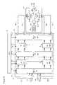
- FIG. 5is a block diagram schematically illustrating principle elements and operations of a PDE compensation system for compensating both first and second order PDE in a Polarization multiplex optical communications system, in accordance with the present invention.
- the present inventionprovides a method and system for mitigating polarization dependent effects (PDEs), including both polarization mode dispersion (PMD) and polarization dependent loss (PDL), in an optical communications system.
- PDEspolarization dependent effects
- FIG. 1is a block diagram schematically illustrating principal elements of a conventional optical communications system in which the present invention may be deployed.
- FIG. 2is a block diagram schematically illustrating principal operations in accordance with the method of the present invention.
- an optical communications systemis represented by a transmitter 2 and a receiver 6 separated by an optical link 4 .
- the link 4may include multiple optical fiber spans separated by active optical devices such as, for example, optical amplifiers, channel equalizers etc. For simplicity of illustration, these elements are not shown in the drawings.
- Signal distortions due to Polarization Mode Dispersion (PMD) and Polarization Dependent Loss (PDL) impressed on optical signals traversing the link 4are represented by a system transfer function T( ⁇ ).
- T( ⁇ )Polarization Mode Dispersion
- PDLPolarization Dependent Loss
- T ⁇ ( ⁇ )exp ⁇ ( 1 2 ⁇ d D d ⁇ ⁇ ⁇ ⁇ ⁇ 2 + D ⁇ ⁇ ⁇ ⁇ ⁇ ⁇ ) ⁇ T ⁇ ( ⁇ c ) ( Eq . ⁇ 1 )
- This transfer function T( ⁇ )is normally formulated using Jones matrix notation of the form:
- T ⁇ ( ⁇ )e ⁇ ⁇ ( ⁇ ) ⁇ [ u 1 ⁇ ( ⁇ ) u 2 ⁇ ( ⁇ ) - u 2 * ⁇ ( ⁇ ) u 1 * ⁇ ( ⁇ ) ] ( Eq . ⁇ 2 )
- T( ⁇ )e ⁇ ⁇ ( ⁇ ) ⁇ [ u 1 ⁇ ( ⁇ ) u 2 ⁇ ( ⁇ ) - u 2 * ⁇ ( ⁇ ) u 1 * ⁇ ( ⁇ ) ]
- a communication signal (or bit-stream) in the form of an electrical input signal x(t) 8is converted into a corresponding optical signal E IN ( ⁇ ) 10 by a conventional Electrical-to-Optical (E/O) converter 12 .
- E/OElectrical-to-Optical
- the received optical signal E OUT ( ⁇ ) 14is converted into a corresponding electrical output signal y(t) 16 by a conventional Optical-to-Electrical (O/E) converter 18 .
- signal distortions due to T( ⁇ )are at least partially compensated by deriving a compensation function C( ⁇ ) that optimizes the optical performance of the link 4 .
- a compensation processor 20uses the compensation function C( ⁇ ) to process the input signal x(t) 8 in the electrical domain, thereby producing a predistorted electrical input signal x 1 (t) 22 .
- the predistorted input signal x 1 (t) 22is then converted into a corresponding predistorted optical signal E 1 IN ( ⁇ ) 10 a by the E/O converter 12 and transmitted through the optical link 4 to the receiver 6 .
- the incoming optical signal E 1 OUT ( ⁇ ) 14 ais converted by the Optical-to-electrical (O/E) converter 18 into a corresponding output signal y 1 (t) 16 a .
- O/EOptical-to-electrical
- the received optical signal E OUT 1 ( ⁇ ) 14 a “seen” by the O/E converter 18will be substantially identical to the original (undistorted) optical signal E IN ( ⁇ ) 10 ( FIG. 1 ).
- the present inventionprovides a technique for compensating distortions impressed upon optical signals traversing the link 4 , by predistorting the input signal x(t) 8 , in the electrical domain, prior to E/O conversion and transmission through the optical link 4 . Because distortion compensation is accomplished in the electrical domain, a substantially arbitrary compensation function C( ⁇ ) can be implemented, thereby facilitating effective compensation of even comparatively severe PDES.
- references to “PDE compensation”, “compensation of PDES” and the likeshould be understood to refer to those PDEs that are compensated by the specific compensation function C( ⁇ ) being used in that embodiment.
- references to a “substantially undistorted optical signal” being obtained at a receiving end of the link 4should be understood to mean that the received optical signal E 1 OUT ( ⁇ ) 14 a is substantially free of signal distortions due to those PDEs that are compensated by the specific compensation function C( ⁇ ) being used in that embodiment.
- the optical signal E 1 OUT ( ⁇ ) 14 a at or near the receiver end of the optical link 4is monitored (at 24 ) in order to detect signal quality parameters indicative of PDEs of the optical link 4 .
- the signal quality parameterscomprise a direct measurement of PMD and/or PDL as a function of wavelength across the wavelength band of interest. Methods of measuring PMD and PDL are known in the art. See, for example, U.S. Pat. No. 5,949,560 (Roberts et al.); “Automated Measurement of Polarization Mode Dispersion Using Jones Matrix Eigenanalysis”, Heffner, IEEE Photonics Technology Letters, Vol.
- any of the signal quality parametersmay be detected based on an optical signal obtained by tapping the optical link 4 (as shown by solid lines in FIG. 2 ), or alternatively by analysis of the output signal y 1 (t) 16 a generated by the E/O converter 18 (as shown by the dashed line in FIG.
- a compensation function C( ⁇ ) which optimizes the detected parameterscan then be derived (at 26) deterministically and/or adaptively, using known techniques.
- the compensation function C( ⁇ )can be expressed as:
- Derivation of the compensation function C( ⁇ ) (at 26 )can then be accomplished by finding appropriate values for T ⁇ 1 ( ⁇ c )X, X ⁇ 1 Y, Y ⁇ 1 , ⁇ 1 , ⁇ 2 , ⁇ 1 , and ⁇ 2 .
- the detected parameterscomprise direct measurement of PMD
- values for T ⁇ 1 ( ⁇ c )X, X ⁇ 1 Y, Y ⁇ 1 , ⁇ 1 , ⁇ 2 , ⁇ 1 and ⁇ 2can be found to minimize (and preferably eliminate) the total PMD. Where bit error rate and/or eye closure are used as proxies, then values can be calculated to optimize the proxy value.
- a compensation function C( ⁇ ) of the same general form as shown above in Eq.4may be used to compensate both PMD and PDL.
- the mathematical manipulations required to incorporate PDL compensation into Eq.4are considered to be well within the perview of those or ordinary skill in the art, and therefore will not be described in further detail.
- the E/O converter 12in order to facilitate PDE compensation, the E/O converter 12 must be designed in such a manner that differential polarization rotations and delays can be impressed onto an optical signal, in addition to amplitude information of the input signal x(t) 8 .
- Various known E/O convertersare capable of providing this functionality.
- the E/O converter 12is provided as a tuned optical source 28 such as a narrow band laser coupled to a pair of conventional 2-dimentional optical modulators 30 .
- a conventional optical power divider 32operates to divide the light from the source 28 into a pair of HE 11 modes, each of which is modulated by a respective one of the 2-D modulators 30 .
- One of the HE 11 modesis subjected to a polarization rotation of 90°, for example using a conventional quarter-wave birefringent plate 34 .
- the modulated HE 11 modesare then combined by a conventional polarization combiner 36 and launched into the optical link 4 .
- each 2-D modulator 30can be independently driven to modulate the amplitude and phase delay of its respective optical mode.
- Various known 2-D optical modulators capable of providing this functionalityare known in the art, such as, for example, Mach-Zehnder modulators.
- FIGS. 3 a and 3 bare block diagrams schematically illustrating principal elements and operations of a compensation processor 18 for compensating first order PMD.
- the E/O converter 12is arranged to launch the predistorted optical signal E 1 IN ( ⁇ ) 10 a with an arbitrary polarization relative to the principle states of polarization of the optical link 4 .
- the compensation function C( ⁇ ) of Eq.4 abovereduces to:
- C ⁇ ( ⁇ )T - 1 ⁇ ( ⁇ c ) ⁇ X ⁇ [ exp ⁇ ( j ⁇ ⁇ ⁇ 1 ⁇ ⁇ ⁇ ⁇ ⁇ ) 0 0 exp ⁇ ( j ⁇ ⁇ ⁇ 2 ⁇ ⁇ ⁇ ⁇ ⁇ ) ] ⁇ X - 1 ( Eq . ⁇ 5 ) and can be implemented within the compensation processor 20 by a pair of matrix multiplier circuits 38 separated by a parallel pair of digital filters 40 . Derivation of the compensation function C( ⁇ ) (at 26 ) can be accomplished by finding appropriate values for T ⁇ 1 ( ⁇ c )X, X ⁇ 1 , ⁇ 1 and ⁇ 2 .
- each 2-D modulator 30is controlled by a respective pair of orthogonal signal components I and Q (at 42 and 44 ) of the predistorted signal x 1 (t) 22 . Consequently, quadrature signal components I and Q (at 46 and 48 ) of the input signal 8 are divided into a pair of compensation paths 50 , each of which is associated with a respective 2-D modulator 30 .
- the first matrix multiplier circuit 38 aoperates to multiply the divided I and Q signal components by the matrix X ⁇ 1 .
- the multiplication result within each compensation path 50is then supplied to a respective digital filter 40 , which filters the signal components in accordance with one of the delay terms ⁇ 1 and ⁇ 2 .
- Various known digital filter typesmay be used to implement the digital filters 40 , such as, for example, Finite Impulse Response (FIR) filters, Infinite Impulse Response (IIR) filters, and Fast Fourier Transform (FFT filters.
- FIRFinite Impulse Response
- IIRInfinite Impulse Response
- FFT filtersFast Fourier Transform
- the output signals I and Q (at 42 and 44 ) generated by the matrix multiplier circuit 38 b of each compensation path 50represent orthogonal (Cartesian) components of the predistorted signal x 1 (t) 22 , and thus provide phase and amplitude information for controlling the associated 2-D modulator 30 . Because the digital filters 40 of each compensation path 50 operate independently, the respective output signals I and Q generated by each compensation path 50 can contain different phase and amplitude information. This enables a different polarization state to be impressed on each of the orthogonal HE 11 modes, which are combined by combiner 36 to produce a predistorted optical signal E 1 IN ( ⁇ ) 10 a having a polarization state that compensates first order PMD of the link 4 .
- first-order PMD and PDLcan be accomplished using exactly the same structure as shown in FIG. 3 a .
- the parameters ⁇ 1 and ⁇ 2will be complex to account for the differential loss/gain of the channel.
- the compensation processor 20can be implemented to generate signal components of the predistorted signal x 1 (t) 22 in any desired format, such as, for example, polar coordinates.
- a suitable 2-D modulator 30must be provided for modulating the appropriate optical components in response to the signals generated by the compensation processor 20 .
- FIG. 3 bis block diagram schematically illustrating principal elements and operations of a first order PMD compensation processor 20 , in which the predistorted optical signal E 1 IN ( ⁇ ) 10 a is launched with a single polarization that is aligned with a principal state of polarization of the optical link 4 .
- the predistorted optical signal E 1 IN ( ⁇ ) 10 ais launched with a single polarization that is aligned with a principal state of polarization of the optical link 4 .
- This compensation function C( ⁇ )can be implemented within the compensation processor 20 by a single matrix multiplier circuit 38 .
- the predistorted optical signal E 1 IN ( ⁇ ) 10 ais aligned with a principal state of polarization of the optical link 4 , it is not necessary to compensate for the delays ⁇ 1 and ⁇ 2 (or the relative delay ⁇ 1 - ⁇ 2 ), and the second matrix multiplier 38 b of FIG. 3 a can also be omitted.
- Derivation of the compensation function C( ⁇ ) (at 26 )can be accomplished by finding an appropriate value for X. With this arrangement, the received optical signal E 1 OUT ( ⁇ ) 14 a will be a delayed and rotated version of the original (undistorted) optical signal E IN ( ⁇ ) 10 ( FIG. 1 ), and will be received without distortion due to first order PMD.
- FIG. 4is a block diagram schematically illustrating principal elements and operations of a compensation processor 20 for compensating both first and second order PMD.
- the compensation function C( ⁇ )conforms to Eq.4 above, and derivation of the compensation function C( ⁇ ) (at 26 ) can be accomplished by finding appropriate values for T ⁇ 1 ( ⁇ c )X, X ⁇ 1 Y, Y ⁇ 1 , ⁇ 1 , ⁇ 2 , ⁇ 1 and ⁇ 2 .
- the derived compensation function C( ⁇ )is implemented within the compensation processor 20 by cascading first, and second order compensation blocks 54 and 56 .
- the first order compensation block 54is substantially identical to that of FIG. 3 a
- the second order compensation block 56comprises a matrix multiplier 58 cascaded with a parallel pair of digital filters 60 .
- quadrature signal components I and Q of the input signal x(t) 8are divided into a pair of compensation paths 50 , each of which is associated with a respective 2-D modulator 30 of the O/E converter 12 .
- the matrix multiplier 58 of the second order PMD compensation block 56operates to multiply the I and Q signal components by the matrix Y ⁇ 1 .
- the multiplication result within each compensation path 50is then supplied to a respective digital filter 60 , which filters the signal components in accordance with the second order matrix term:
- Various known digital filter typesmay be used to implement the digital filters 60 , such as, for example, Finite Impulse Response (FIR) filters, Infinite Impulse Response (IIR) filters, and Fast Fourier Transform (FFT) filters.
- FIRFinite Impulse Response
- IIRInfinite Impulse Response
- FFTFast Fourier Transform
- the output signals generated by the digital filters 60 of each compensation path 50are then multiplied by the matrix X ⁇ 1 Y, using the matrix multiplier 38 a of the first order compensation block 54 .
- the multiplication result generated by the matrix multiplier 38 a within each compensation path 50is then supplied to a respective digital filter 40 , which filters the signal components in accordance with the first order delay:
- the filtered signal componentsare then multipled, by the third matrix multiplier 38 b , in accordance with T ⁇ 1 ( ⁇ c )X.
- the output signals I and Q (at 42 and 44 ) of each compensation path 50represent orthogonal (Cartesian) components of the predistorted signal x 1 (t) 22 , and thus provide phase and amplitude information for controlling the associated 2-D modulator 30 .
- the primary difference between the embodiments of FIGS. 3 a and 4is that the addition of the second order compensation block 56 enables the compensation function C( ⁇ ) to be defined to more closely compensate distortions introduced by the transfer function T( ⁇ ).
- the compensation function C( ⁇ )may be derived to include terms for third order through to nth order PDEs, each order of compensation can then be implemented in the compensation processor 20 by means of a respective compensation block that is closely similar to the second order compensation block 56 , including respective complex multiplier 58 and digital filters 60 .
- the compensation function C( ⁇ )is derived to compensate signal distortions imposed on optical signals traversing the optical link 4 due to PDEs of the link 4 .
- this functionalitycan be obtained independently of the modulation scheme used to encode the bit stream into the optical signal.
- the compensation function C( ⁇ )operates on the input signal x(t) 8 in the electrical domain to define a desired polarization state of the predistorted optical signal E 1 IN ( ⁇ ) 10 a launched into the link 4 by the E/O converter 12 .
- any arbitrary polarization statemay be obtained in the manner, by suitable selection of the parameter values of the compensation function C( ⁇ ).
- the embodiment of FIG. 4which implements the compensation function C( ⁇ ) of Eq.4, can be modified to produce polarization modulation of the input signal x(t) 8 .
- a further modification of the embodiment of FIG. 4can be used to implement polarization interleaving of a pair of parallel input signals x 1 (t) 8 a and x 2 (t) 8 b , as shown in FIG. 5 .
- E/O and O/E converters 12 and 18and chromatic dispersion in the optical link 4 will normally cause signal distortions additional to those of PDEs.
- the scalar transfer function H( ⁇ )can be compensated independently of the PDE compensation described above with reference to FIGS. 2-5 , for example by inserting a digital filter (not shown) upstream of the compensation processor 20 .
Landscapes
- Physics & Mathematics (AREA)
- Electromagnetism (AREA)
- Engineering & Computer Science (AREA)
- Computer Networks & Wireless Communication (AREA)
- Signal Processing (AREA)
- Optical Communication System (AREA)
Abstract
Description
A directly analogous derivation of the transfer function T(ω), incorporating the effects of Polarization Dependent Loss (PDL), can be performed, and yields a Taylor expansion and Jones matrix of substantially the same form as shown in
EOUT1(ω)=T(ω)EIN1(ω)=T(ω)C(ω)EIN(ω) (Eq.3)
As may be appreciated, when the distortions introduced by the compensation function C(ω) exactly counterbalance those introduced by the system transfer function T(ω), the received optical signal EOUT1(ω)14a“seen” by the O/
With this formulation, the matrices T−1(ωc)X, X−1Y and Y−1can be implemented within the
implemented by known digital filter blocks such as Finite Impulse Response (FIR), Infinite Impulse Response (IIR) and Fast Fourier Transform (FFT) filters. Derivation of the compensation function C(ω) (at26) can then be accomplished by finding appropriate values for T−1(ωc)X, X−1Y, Y−1, β1, β2, Γ1, and Γ2. In embodiments in which the detected parameters comprise direct measurement of PMD, values for T−1(ωc)X, X−1Y, Y−1, β1, β2, Γ1and Γ2can be found to minimize (and preferably eliminate) the total PMD. Where bit error rate and/or eye closure are used as proxies, then values can be calculated to optimize the proxy value.
and can be implemented within the
and the compensation function C(ω) of Eq.5 above reduces to:
C(ω)=X (Eq.7)
where now
T(ω)=T(ωc)·exp(Dδω)
Various known digital filter types may be used to implement the digital filters60, such as, for example, Finite Impulse Response (FIR) filters, Infinite Impulse Response (IIR) filters, and Fast Fourier Transform (FFT) filters.
Finally, the filtered signal components are then multipled, by the
EOUT1(ω)=T(ω)EIN1(ω)≅EIN(ω) (Eq.8)
EOUT1(ω)=H(ω)·T(ω)·EIN1(ω)≅EIN(ω) (Eq.9)
The scalar transfer function H(ω) can be compensated independently of the PDE compensation described above with reference to
Claims (33)
Priority Applications (5)
| Application Number | Priority Date | Filing Date | Title |
|---|---|---|---|
| US10/307,466US7382985B2 (en) | 2002-12-02 | 2002-12-02 | Electrical domain mitigation of polarization dependent effects in an optical communications system |
| EP03757590AEP1554822B1 (en) | 2002-10-03 | 2003-10-03 | Electrical domain mitigation of polarization dependent effects in an optical communications system |
| US10/677,223US7023601B2 (en) | 2002-12-02 | 2003-10-03 | Optical E-field modulation using a Mach-Zehnder interferometer |
| PCT/CA2003/001532WO2004032386A1 (en) | 2002-10-03 | 2003-10-03 | Electrical domain mitigation of polarization dependent effects in an optical communications system |
| AU2003273683AAU2003273683A1 (en) | 2002-10-03 | 2003-10-03 | Electrical domain mitigation of polarization dependent effects in an optical communications system |
Applications Claiming Priority (1)
| Application Number | Priority Date | Filing Date | Title |
|---|---|---|---|
| US10/307,466US7382985B2 (en) | 2002-12-02 | 2002-12-02 | Electrical domain mitigation of polarization dependent effects in an optical communications system |
Related Parent Applications (1)
| Application Number | Title | Priority Date | Filing Date |
|---|---|---|---|
| US10/405,236Continuation-In-PartUS7756421B2 (en) | 2002-10-03 | 2003-04-03 | Electrical domain compensation of non-linear effects in an optical communications system |
Related Child Applications (1)
| Application Number | Title | Priority Date | Filing Date |
|---|---|---|---|
| US10/677,223Continuation-In-PartUS7023601B2 (en) | 2002-12-02 | 2003-10-03 | Optical E-field modulation using a Mach-Zehnder interferometer |
Publications (2)
| Publication Number | Publication Date |
|---|---|
| US20040105682A1 US20040105682A1 (en) | 2004-06-03 |
| US7382985B2true US7382985B2 (en) | 2008-06-03 |
Family
ID=32392565
Family Applications (1)
| Application Number | Title | Priority Date | Filing Date |
|---|---|---|---|
| US10/307,466Expired - LifetimeUS7382985B2 (en) | 2002-10-03 | 2002-12-02 | Electrical domain mitigation of polarization dependent effects in an optical communications system |
Country Status (1)
| Country | Link |
|---|---|
| US (1) | US7382985B2 (en) |
Cited By (25)
| Publication number | Priority date | Publication date | Assignee | Title |
|---|---|---|---|---|
| US20070206954A1 (en)* | 2006-03-03 | 2007-09-06 | Fishman Daniel A | Simultaneous electrical pre-compensation of self-phase modulation and chromatic dispersion |
| US20080050125A1 (en)* | 2006-05-11 | 2008-02-28 | Rene Jean Essiambre | Intra-channel nonlinearity compensation for optical data communications |
| US20080082597A1 (en)* | 2006-09-29 | 2008-04-03 | Optichron, Inc. | Low power and low complexity adaptive self-linearization |
| US20080082280A1 (en)* | 2006-09-29 | 2008-04-03 | Optichron, Inc. | Adaptive self-linearization with separation filter |
| US20080082281A1 (en)* | 2006-09-29 | 2008-04-03 | Optichron, Inc. | Adaptive self-linearization |
| US20080270082A1 (en)* | 2006-09-29 | 2008-10-30 | Optichron, Inc. | Low-power and low-cost adaptive self-linearization system with fast convergence |
| US20080288199A1 (en)* | 2006-09-29 | 2008-11-20 | Optichron, Inc. | Distortion cancellation using adaptive linearization |
| US20090074427A1 (en)* | 2007-09-14 | 2009-03-19 | Xiang Liu | Reconstruction and restoration of two polarization components of an optical signal field |
| US20090214224A1 (en)* | 2007-04-03 | 2009-08-27 | Celight, Inc. | Method and apparatus for coherent analog rf photonic transmission |
| US20100092181A1 (en)* | 2008-02-13 | 2010-04-15 | Nortel Neteworks Limited | Low conversion rate digital dispersion compensation |
| US20100329694A1 (en)* | 2009-06-24 | 2010-12-30 | Frankel Michael Y | Electrical domain suppression of linear crosstalk in optical communication systems |
| US20100329677A1 (en)* | 2009-06-29 | 2010-12-30 | Noriaki Kaneda | Symbol Timing Recovery in Polarization Division Multiplexed Coherent Optical Transmission System |
| US8160453B1 (en)* | 2006-03-30 | 2012-04-17 | Rockstar Bidco, LP | Protection switching with transmitter compensation function |
| US20120148260A1 (en)* | 2010-12-13 | 2012-06-14 | Fujitsu Limited | Optical transmitter and optical transmission method |
| US20130051801A1 (en)* | 2009-12-15 | 2013-02-28 | Maxim Kuschnerov | Method and Arrangement for Transmitting an Optical Transmission Signal with Reduced Polarisation-Dependent Loss |
| US20140029938A1 (en)* | 2012-07-26 | 2014-01-30 | Fujitsu Limited | Optical transmission system and method for monitoring polarization dependent characteristics of optical transmission line |
| US9172471B2 (en) | 2013-03-15 | 2015-10-27 | The United States Of America, As Represented By The Secretary Of The Navy | System and method for suppression of even-order photodiode distortions |
| US20160099775A1 (en)* | 2014-10-01 | 2016-04-07 | Futurewei Technologies, Inc. | Optical Transmitter with Optical Receiver-Specific Dispersion Pre-Compensation |
| US20160285558A1 (en)* | 2013-04-04 | 2016-09-29 | Nec Corporation | Digital optical transmitter, optical communication system using the same, and digital optical transmission method |
| US9768876B1 (en) | 2016-07-27 | 2017-09-19 | The Government Of The United States Of America, As Represented By The Secretary Of The Navy | Method of suppressing polarization-dependent loss in polarization-modulated photonic links |
| CN109104247A (en)* | 2018-09-17 | 2018-12-28 | 中国电子科技集团公司第三十八研究所 | The steady phase Transmission system of broadband signal based on microwave photon link |
| US10389447B1 (en) | 2018-06-08 | 2019-08-20 | Ciena Corporation | Dimensional transformation |
| US10797803B2 (en)* | 2018-03-29 | 2020-10-06 | Shanghai Jiao Tong University | Waveform matching based optical digital signal receiving device |
| US20220224417A1 (en)* | 2021-01-14 | 2022-07-14 | Fujitsu Limited | Transmission device and method of setting transmission parameter |
| US11799560B2 (en) | 2019-10-31 | 2023-10-24 | Ciena Corporation | Asymmetric direct detection of optical signals |
Families Citing this family (32)
| Publication number | Priority date | Publication date | Assignee | Title |
|---|---|---|---|---|
| US7460793B2 (en)* | 2002-12-11 | 2008-12-02 | Michael George Taylor | Coherent optical detection and signal processing method and system |
| US7373087B2 (en)* | 2003-02-27 | 2008-05-13 | Oplink Communications, Inc. | Adaptive optical transponder |
| US7742701B2 (en)* | 2005-03-16 | 2010-06-22 | Michael George Taylor | Coherent optical channel substitution |
| US9520950B2 (en)* | 2008-06-10 | 2016-12-13 | Ciena Corporation | Optical communications system having chromatic dispersion and polarization mode dispersion compensation |
| US9300400B2 (en) | 2011-09-16 | 2016-03-29 | Alcatel Lucent | Communication through multiplexed one-dimensional optical signals |
| JP5839050B2 (en)* | 2012-02-03 | 2016-01-06 | 富士通株式会社 | Optical transmission system and optical signal transmission method |
| US8977137B2 (en)* | 2012-07-18 | 2015-03-10 | Fujitsu Limited | Polarization dependent loss compensation |
| WO2014040619A1 (en)* | 2012-09-12 | 2014-03-20 | Telefonaktiebolaget L M Ericsson (Publ) | Detecting optical fibre stress in an optical communications network |
| ES2880838T3 (en)* | 2014-04-15 | 2021-11-25 | Arris Entpr Llc | Smart receivers and transmitters for CATV networks |
| JP6279500B2 (en)* | 2015-02-18 | 2018-02-14 | 日本電信電話株式会社 | Optical communication system and optical communication method |
| JP6485095B2 (en)* | 2015-02-18 | 2019-03-20 | 富士通株式会社 | Optical transmission device, optical transmission system, and polarization dependent loss monitor |
| US10236982B1 (en)* | 2017-12-21 | 2019-03-19 | Ciena Corporation | Fiber parameter identification |
| US11251878B2 (en) | 2018-02-07 | 2022-02-15 | Infinera Corporation | Independently routable digital subcarriers for optical communication networks |
| US11368228B2 (en) | 2018-04-13 | 2022-06-21 | Infinera Corporation | Apparatuses and methods for digital subcarrier parameter modifications for optical communication networks |
| US11095389B2 (en) | 2018-07-12 | 2021-08-17 | Infiriera Corporation | Subcarrier based data center network architecture |
| US11075694B2 (en) | 2019-03-04 | 2021-07-27 | Infinera Corporation | Frequency division multiple access optical subcarriers |
| US11258528B2 (en) | 2019-09-22 | 2022-02-22 | Infinera Corporation | Frequency division multiple access optical subcarriers |
| US11336369B2 (en) | 2019-03-22 | 2022-05-17 | Infinera Corporation | Framework for handling signal integrity using ASE in optical networks |
| US11418312B2 (en) | 2019-04-19 | 2022-08-16 | Infinera Corporation | Synchronization for subcarrier communication |
| US10972184B2 (en) | 2019-05-07 | 2021-04-06 | Infinera Corporation | Bidirectional optical communications |
| US11476966B2 (en) | 2019-05-14 | 2022-10-18 | Infinera Corporation | Out-of-band communication channel for subcarrier-based optical communication systems |
| US11239935B2 (en)* | 2019-05-14 | 2022-02-01 | Infinera Corporation | Out-of-band communication channel for subcarrier-based optical communication systems |
| US10965378B2 (en)* | 2019-05-14 | 2021-03-30 | Infinera Corporation | Out-of-band communication channel for sub-carrier-based optical communication systems |
| US11296812B2 (en) | 2019-05-14 | 2022-04-05 | Infinera Corporation | Out-of-band communication channel for subcarrier-based optical communication systems |
| US11190291B2 (en) | 2019-05-14 | 2021-11-30 | Infinera Corporation | Out-of-band communication channel for subcarrier-based optical communication systems |
| US11489613B2 (en) | 2019-05-14 | 2022-11-01 | Infinera Corporation | Out-of-band communication channel for subcarrier-based optical communication systems |
| JP6693592B1 (en)* | 2019-05-22 | 2020-05-13 | Nttエレクトロニクス株式会社 | Optical transmission characteristic compensation method and optical transmission characteristic compensation system |
| US11297005B2 (en) | 2019-09-05 | 2022-04-05 | Infiriera Corporation | Dynamically switching queueing schemes for network switches |
| EP4042607A1 (en) | 2019-10-10 | 2022-08-17 | Infinera Corporation | Network switches systems for optical communications networks |
| AU2020364088B2 (en) | 2019-10-10 | 2025-04-17 | Infinera Corporation | Optical subcarrier dual-path protection and restoration for optical communications networks |
| US11356180B2 (en) | 2019-10-10 | 2022-06-07 | Infinera Corporation | Hub-leaf laser synchronization |
| US11546058B1 (en)* | 2020-01-29 | 2023-01-03 | Cable Television Laboratories, Inc. | Systems and methods for chromatic dispersion pre-compensation |
Citations (36)
| Publication number | Priority date | Publication date | Assignee | Title |
|---|---|---|---|---|
| US5148503A (en) | 1991-05-29 | 1992-09-15 | Crystal Technology, Inc | Apparatus and method for linearized cascade coupled integrated optical modulator |
| EP0524758A2 (en) | 1991-07-23 | 1993-01-27 | AT&T Corp. | Distortion compensation for analog optical systems |
| US5311346A (en) | 1992-06-17 | 1994-05-10 | At&T Bell Laboratories | Fiber-optic transmission polarization-dependent distortion compensation |
| US5349312A (en) | 1993-05-28 | 1994-09-20 | Raytheon Company | Voltage variable attenuator |
| US5408498A (en) | 1991-07-03 | 1995-04-18 | Sharp Kabushiki Kaisha | Serial-signal transmission apparatus |
| US5416626A (en) | 1993-02-02 | 1995-05-16 | Northern Telecom Limited | Optically amplified transmission systems |
| US5513029A (en) | 1994-06-16 | 1996-04-30 | Northern Telecom Limited | Method and apparatus for monitoring performance of optical transmission systems |
| US5579328A (en) | 1995-08-10 | 1996-11-26 | Northern Telecom Limited | Digital control of laser diode power levels |
| US5761225A (en) | 1996-05-23 | 1998-06-02 | Litton Systems, Inc. | Optical fiber amplifier eled light source with a relative intensity noise reduction system |
| US5892858A (en) | 1997-03-27 | 1999-04-06 | Northern Telecom Limited | Duobinary coding and modulation technique for optical communication systems |
| US5949560A (en) | 1997-02-05 | 1999-09-07 | Northern Telecom Limited | Optical transmission system |
| US5999258A (en) | 1997-06-26 | 1999-12-07 | Nortel Networks Corporation | Optical interference measurement method and system |
| US6067180A (en) | 1997-06-09 | 2000-05-23 | Nortel Networks Corporation | Equalization, pulse shaping and regeneration of optical signals |
| DE19852597A1 (en)* | 1998-11-14 | 2000-05-25 | Alcatel Sa | Data communications system with electronic polarization mode dispersion distortion correction has transmitter with pre-distortion device, receiver for signals at more than two levels |
| US6115162A (en) | 1995-01-10 | 2000-09-05 | Harris Corporation | Double side band, carrier suppressed modulated coherent fiber optic link |
| US6124960A (en) | 1997-09-08 | 2000-09-26 | Northern Telecom Limited | Transmission system with cross-phase modulation compensation |
| US6128111A (en) | 1996-12-19 | 2000-10-03 | Nortel Networks Corporation | Monitoring of nonlinear effects |
| WO2001003339A1 (en) | 1999-06-30 | 2001-01-11 | Koninklijke Philips Electronics N.V. | Pre-shaping laser modulation signals to increase modulation index |
| US6205262B1 (en) | 1997-05-01 | 2001-03-20 | Alliance Fiber Optics Products, Inc. | Optical recirculation depolarizer and method of depolarizing light |
| US6236488B1 (en)* | 1997-03-31 | 2001-05-22 | Mitsubishi Denki Kabushiki Kaisha | Optical pulse position detecting circuit and an optical pulse generating apparatus and their methods |
| US6262834B1 (en) | 2000-02-23 | 2001-07-17 | The United States Of America As Represented By The Secretary Of The Navy | Wideband single sideband modulation of optical carriers |
| US6301550B1 (en)* | 1997-11-28 | 2001-10-09 | Mitutoyo Corporation | Phase delay correction system |
| US20010028760A1 (en) | 2000-03-03 | 2001-10-11 | Yaffe Henry H. | Methods and apparatus for compensating chromatic and polarization mode dispersion |
| US6304369B1 (en) | 1999-07-29 | 2001-10-16 | Harmonic, Inc. | Method and apparatus for eliminating noise in analog fiber links |
| WO2001091342A2 (en) | 2000-05-24 | 2001-11-29 | Purdue Research Foundation | Method and system for polarization control and polarization mode dispersion compensation for wideband optical signals |
| US20020018268A1 (en) | 1998-11-04 | 2002-02-14 | Corvis Corporation Attn: Intellectual Property Department | Optical distortion compensation apparatuses, methods, and systems |
| US20020024694A1 (en)* | 2000-05-12 | 2002-02-28 | Newell Laurence J. | Control channel for an optical communications system utilizing frequency division multiplexing |
| WO2002043340A2 (en) | 2000-11-22 | 2002-05-30 | Broadcom Corporation | Method and apparatus to identify and characterize nonlinearities in optical communications channels |
| US20020106148A1 (en) | 1999-05-24 | 2002-08-08 | Philips Electronics North America Corporation | Optical communication with pre-compensation for odd order distortion in modulation and transmission |
| US6441932B1 (en) | 1999-02-09 | 2002-08-27 | The United States Of America As Represented By The Secretary Of The Air Force | Intensity noise suppression using differential delay cancellation in external modulation links |
| EP1237307A2 (en) | 2001-03-02 | 2002-09-04 | Fujitsu Limited | Receiving apparatus and method for detecting, measuring and compensating waveform degradation of received signal |
| US6473013B1 (en) | 2001-06-20 | 2002-10-29 | Scott R. Velazquez | Parallel processing analog and digital converter |
| US20030011847A1 (en) | 2001-06-07 | 2003-01-16 | Fa Dai | Method and apparatus for adaptive distortion compensation in optical fiber communication networks |
| US6559994B1 (en) | 1999-08-18 | 2003-05-06 | New Elite Technologies, Inc. | Optical fiber transmitter for long distance subcarrier multiplexed lightwave systems |
| US6580532B1 (en) | 1999-01-28 | 2003-06-17 | California Institute Of Technology | Opto-electronic techniques for reducing phase noise in a carrier signal by carrier supression |
| US20040197103A1 (en)* | 2002-10-03 | 2004-10-07 | Nortel Networks Limited | Electrical domain compensation of non-linear effects in an optical communications system |
Family Cites Families (1)
| Publication number | Priority date | Publication date | Assignee | Title |
|---|---|---|---|---|
| DE3889733T2 (en)* | 1987-07-24 | 1994-09-08 | Terumo Corp | DEVICE FOR MEASURING THE CONCENTRATION AND OXYGEN SATURATION OF HEMOGLOBIN. |
- 2002
- 2002-12-02USUS10/307,466patent/US7382985B2/ennot_activeExpired - Lifetime
Patent Citations (36)
| Publication number | Priority date | Publication date | Assignee | Title |
|---|---|---|---|---|
| US5148503A (en) | 1991-05-29 | 1992-09-15 | Crystal Technology, Inc | Apparatus and method for linearized cascade coupled integrated optical modulator |
| US5408498A (en) | 1991-07-03 | 1995-04-18 | Sharp Kabushiki Kaisha | Serial-signal transmission apparatus |
| EP0524758A2 (en) | 1991-07-23 | 1993-01-27 | AT&T Corp. | Distortion compensation for analog optical systems |
| US5311346A (en) | 1992-06-17 | 1994-05-10 | At&T Bell Laboratories | Fiber-optic transmission polarization-dependent distortion compensation |
| US5416626A (en) | 1993-02-02 | 1995-05-16 | Northern Telecom Limited | Optically amplified transmission systems |
| US5349312A (en) | 1993-05-28 | 1994-09-20 | Raytheon Company | Voltage variable attenuator |
| US5513029A (en) | 1994-06-16 | 1996-04-30 | Northern Telecom Limited | Method and apparatus for monitoring performance of optical transmission systems |
| US6115162A (en) | 1995-01-10 | 2000-09-05 | Harris Corporation | Double side band, carrier suppressed modulated coherent fiber optic link |
| US5579328A (en) | 1995-08-10 | 1996-11-26 | Northern Telecom Limited | Digital control of laser diode power levels |
| US5761225A (en) | 1996-05-23 | 1998-06-02 | Litton Systems, Inc. | Optical fiber amplifier eled light source with a relative intensity noise reduction system |
| US6128111A (en) | 1996-12-19 | 2000-10-03 | Nortel Networks Corporation | Monitoring of nonlinear effects |
| US5949560A (en) | 1997-02-05 | 1999-09-07 | Northern Telecom Limited | Optical transmission system |
| US5892858A (en) | 1997-03-27 | 1999-04-06 | Northern Telecom Limited | Duobinary coding and modulation technique for optical communication systems |
| US6236488B1 (en)* | 1997-03-31 | 2001-05-22 | Mitsubishi Denki Kabushiki Kaisha | Optical pulse position detecting circuit and an optical pulse generating apparatus and their methods |
| US6205262B1 (en) | 1997-05-01 | 2001-03-20 | Alliance Fiber Optics Products, Inc. | Optical recirculation depolarizer and method of depolarizing light |
| US6067180A (en) | 1997-06-09 | 2000-05-23 | Nortel Networks Corporation | Equalization, pulse shaping and regeneration of optical signals |
| US5999258A (en) | 1997-06-26 | 1999-12-07 | Nortel Networks Corporation | Optical interference measurement method and system |
| US6124960A (en) | 1997-09-08 | 2000-09-26 | Northern Telecom Limited | Transmission system with cross-phase modulation compensation |
| US6301550B1 (en)* | 1997-11-28 | 2001-10-09 | Mitutoyo Corporation | Phase delay correction system |
| US20020018268A1 (en) | 1998-11-04 | 2002-02-14 | Corvis Corporation Attn: Intellectual Property Department | Optical distortion compensation apparatuses, methods, and systems |
| DE19852597A1 (en)* | 1998-11-14 | 2000-05-25 | Alcatel Sa | Data communications system with electronic polarization mode dispersion distortion correction has transmitter with pre-distortion device, receiver for signals at more than two levels |
| US6580532B1 (en) | 1999-01-28 | 2003-06-17 | California Institute Of Technology | Opto-electronic techniques for reducing phase noise in a carrier signal by carrier supression |
| US6441932B1 (en) | 1999-02-09 | 2002-08-27 | The United States Of America As Represented By The Secretary Of The Air Force | Intensity noise suppression using differential delay cancellation in external modulation links |
| US20020106148A1 (en) | 1999-05-24 | 2002-08-08 | Philips Electronics North America Corporation | Optical communication with pre-compensation for odd order distortion in modulation and transmission |
| WO2001003339A1 (en) | 1999-06-30 | 2001-01-11 | Koninklijke Philips Electronics N.V. | Pre-shaping laser modulation signals to increase modulation index |
| US6304369B1 (en) | 1999-07-29 | 2001-10-16 | Harmonic, Inc. | Method and apparatus for eliminating noise in analog fiber links |
| US6559994B1 (en) | 1999-08-18 | 2003-05-06 | New Elite Technologies, Inc. | Optical fiber transmitter for long distance subcarrier multiplexed lightwave systems |
| US6262834B1 (en) | 2000-02-23 | 2001-07-17 | The United States Of America As Represented By The Secretary Of The Navy | Wideband single sideband modulation of optical carriers |
| US20010028760A1 (en) | 2000-03-03 | 2001-10-11 | Yaffe Henry H. | Methods and apparatus for compensating chromatic and polarization mode dispersion |
| US20020024694A1 (en)* | 2000-05-12 | 2002-02-28 | Newell Laurence J. | Control channel for an optical communications system utilizing frequency division multiplexing |
| WO2001091342A2 (en) | 2000-05-24 | 2001-11-29 | Purdue Research Foundation | Method and system for polarization control and polarization mode dispersion compensation for wideband optical signals |
| WO2002043340A2 (en) | 2000-11-22 | 2002-05-30 | Broadcom Corporation | Method and apparatus to identify and characterize nonlinearities in optical communications channels |
| EP1237307A2 (en) | 2001-03-02 | 2002-09-04 | Fujitsu Limited | Receiving apparatus and method for detecting, measuring and compensating waveform degradation of received signal |
| US20030011847A1 (en) | 2001-06-07 | 2003-01-16 | Fa Dai | Method and apparatus for adaptive distortion compensation in optical fiber communication networks |
| US6473013B1 (en) | 2001-06-20 | 2002-10-29 | Scott R. Velazquez | Parallel processing analog and digital converter |
| US20040197103A1 (en)* | 2002-10-03 | 2004-10-07 | Nortel Networks Limited | Electrical domain compensation of non-linear effects in an optical communications system |
Non-Patent Citations (32)
| Title |
|---|
| A. Mecozzi et al. "Cancellation of timing and Amplitude Jitter in Symmetric Links Using Highly Dispersed Pulses", IEEE Photonics Technology Letters, vol. 13, No. 5, May 2001, pp. 445-447, USA. |
| Adaptive Electronic Linearization of Fiber Optic Links, OFC 2003, vol. 2, pp. 477-480, Mar. 2003, Sadhwani et al. |
| Andre, P.S. et al "Extraction of DFB Laser Rate Equations Parameters for Optical Simulation Purposes", Conftele 99 ISBN 972-98115-0-4, pp. 561-564, 1999. |
| Automated Measurement of Polarization Mode Dispersion Using Jones Matrix Eigenanalysis, IEE Photonics Technology Letters, vol. 4, No. 9, pp. 1066-1069, Sep. 1992, Heffner. |
| Bulow, Henning et al "Dispersion Mitigation Using a Fiber-Bragg-Grating Sideband Filter and a Tunable Electronic Equalizer", WDD34, pp. 1-4, 2001. |
| Chromatic Dispersion Mapping by Sensing the Power Distribution of Four-Wave Mixing Along the Fiber Using Brillouin Probing, OFC 2003, vol. 2, pp. 714-716, Herraez et al. |
| Design of Broad-Band PMD Compensation Filters, IEE Photonics Technology Letters, vol. 14, No. 8, pp. 1088-1090, Aug. 2002, Eyal et al. |
| Dispersion Compensation by Active Predistorted Signal Synthesis, Journal of Lightwave Technology, vol. LT-3, No. 4, Aug. 1985, Thomas L. Koch and Rod C. Alferness. |
| Dispersion Compensation with an SBS-Suppressed Fiber Phase Conjugator Using Synchronized Phase Modulation, OFC 2003, vol. 2, pp. 716-717, M. Tani. |
| Electrical Signal Processing Techniques in Long-Haul Fiber-Optic Systems, 1990 IEEE-Transactions on Communications, vol. 38, No. 9, Jack H. Winters, et al. |
| Exact Compensation for both Chromatic Dispersion and Kerr Effect in a Transmission Fiber Using Optical Phase Conjunction, Journal of Lightwave Technology, vol. 14, No. 3, Mar. 1996, Watanabe et al. |
| Feldhaus, G: "Volterra Equalizer for Electrical for Electrical Compensation of Dispersion and Fiber Nonlinearities", Journal of Optical Communications, Fachverlag Schiele & Schon, Berlin, De, vol. 23, No. 3, Jun. 2002, pp. 82-84, XP001130377, ISSN: 0173-4911. |
| High-Dynamic-Range Laser Amplitude and Phase Noise Measurement Techniques, IEEE Journal on Selected Topics in Quantum Electronics, vol. 7, No. 4, Jul./Aug. 2001, Ryan P. Scott et al. |
| Illing, Lucas et al "Shaping current waveforms for direct modulation of semiconductor lasers", Institute for Nonlinear Science, 2003, San Diego, U.S.A. |
| Kamotoa, T. et al "An 8-bit 2-ns Monolithic DAC", IEEE Journal of Solid-State Circuits, Feb. 1988, vol. 23, No. 1. |
| Kim, Hoon et al "10 Gbit/s 177 km transmission over conventional singlemode fibre using a vestigial side-band modulation format", Electronics Letters, Dec. 6, 2001, pp. 1533-1534, vol. 37, No. 25. |
| Measurement of High-Order Polarization Mode Dispersion, IEE Photonics Technology Letters, vol. 12, No. 7, pp. 861-863, Jul. 2000, Li et al. |
| Mitigation of Dispersion-Induced Effects Using SOA in Analog Optical Transmission, IEEE Photonics Technology Letters, vol. 14, No. 8, Aug. 2002, Duk-Ho Jeon et al. |
| Performance of Smart Lightwave Receivers With Linear Equalization, Journal of Lightwave Technology, vol. 10, No. 8, Aug. 1992, John C. Cartledge, et al. |
| Polarization Effects in Lightwave Systems, Craig D. Poole and Jonathan Nagel, 1997. |
| Polarization Modulated Direct Detection Optical Transmission Systems, Journal of Lightwave Technology, vol. 10, No. 12, pp. 1985-1997, Dec. 1992, Betti et al. |
| Predistortion of Electroabsorption Modulators for Analog CATV Systems at 1.55*m, Journal of Lightwave Technology, vol. 15, No. 9, Sep. 1997, Gordon C. Wilson et al. |
| Predistortion Techniques for Linearization of External Modulators, 1999 IEEE-Gordon Wilson, Lucent Technologies, NJ 07733, U.S.A. |
| Reduction of Dispersion-Induced Distortion in SCM Transmission Systems by Using Predistortion-Linearized MQW-EA Modulatirs, Journal of Lightwave Technology, vol. 15, No. 2, Feb. 1997, T. Iwai et al. |
| Representation of second order polarization mode dispersion, Electronics Letters, vol. 35, No. 19, pp. 1658-1659, Sep. 16, 1999, Marshall et al. |
| Sadhwani, Ram et al "Adaptive CMOS Predistortion Linearizer for Fiber-Optic Links", Journal of Lightwave Technology, Dec. 2003, pp. 3180-3193, vol. 21, No. 12., U.S.A. |
| Schaffer, Troy A. et al "A 2GHz 12-bit Digital-to-Analog Converter for Direct Digital Synthesis Applications", GaAs IC Symposium, pp. 61-64, 1996. |
| Sieben, M. et al "10Gbit/s optical single sideband system", Electronics Letters, May 22, 1997, pp. 971-9733, vol. 33, No. 11. |
| Signal Distortion and Noise in AM-SCM Transmission Systems Employing the Feedfrorward Linearized MQW-EA External Modulator, Journal of Lightwave Technology, vol. 15, No. 8, Aug. 1995, T. Iwai et al. |
| Soliton Transmission Using Periodic Dispersion Compensation, Journal of Lightwave Technology, vol. 15, No. 10, Oct. 1997, Nicholas J. Smith et al. |
| Theoretical Basis of Polarization Mode Dispersion Equalization up to the Second Order, Journal of Lightwave Technology, vol. 18, No. 4, pp. 614-617, Apr. 2000, Kudou et al. |
| Watts, P.M. et al "Demonstration of Electrical Dispersion Compensation of Single Sideband Optical Transmission", Optical Networks Group, Dept. of Electronic and Electrical Engineering, University College London, Torrington Place, London. 2003. |
Cited By (50)
| Publication number | Priority date | Publication date | Assignee | Title |
|---|---|---|---|---|
| US20070206954A1 (en)* | 2006-03-03 | 2007-09-06 | Fishman Daniel A | Simultaneous electrical pre-compensation of self-phase modulation and chromatic dispersion |
| US7660537B2 (en)* | 2006-03-03 | 2010-02-09 | Alcatel-Lucent Usa Inc. | Simultaneous electrical pre-compensation of self-phase modulation and chromatic dispersion |
| US8682179B1 (en) | 2006-03-30 | 2014-03-25 | Rockstar Consortium Us Lp | Protection switching with transmitter compensation function |
| US8160453B1 (en)* | 2006-03-30 | 2012-04-17 | Rockstar Bidco, LP | Protection switching with transmitter compensation function |
| US8879904B1 (en) | 2006-03-30 | 2014-11-04 | Rockstar Consortium Us Lp | Protection switching with transmitter compensation function |
| US7672599B2 (en)* | 2006-05-11 | 2010-03-02 | Alcatel-Lucent Usa Inc. | Intra-channel nonlinearity compensation for optical data communications |
| US20080050125A1 (en)* | 2006-05-11 | 2008-02-28 | Rene Jean Essiambre | Intra-channel nonlinearity compensation for optical data communications |
| US8660820B2 (en) | 2006-09-29 | 2014-02-25 | Netlogic Microsystems, Inc. | Distortion cancellation using adaptive linearization |
| US8620981B2 (en) | 2006-09-29 | 2013-12-31 | Netlogic Microsystems, Inc. | Low power and low complexity adaptive self-linearization |
| US20080082281A1 (en)* | 2006-09-29 | 2008-04-03 | Optichron, Inc. | Adaptive self-linearization |
| US9197262B2 (en) | 2006-09-29 | 2015-11-24 | Broadcom Corporation | Low-power and low-cost adaptive self-linearization system with fast convergence |
| US7693672B2 (en) | 2006-09-29 | 2010-04-06 | Optichron | Adaptive self-linearization |
| US20080288199A1 (en)* | 2006-09-29 | 2008-11-20 | Optichron, Inc. | Distortion cancellation using adaptive linearization |
| US20080082280A1 (en)* | 2006-09-29 | 2008-04-03 | Optichron, Inc. | Adaptive self-linearization with separation filter |
| US20080270082A1 (en)* | 2006-09-29 | 2008-10-30 | Optichron, Inc. | Low-power and low-cost adaptive self-linearization system with fast convergence |
| US20080082597A1 (en)* | 2006-09-29 | 2008-04-03 | Optichron, Inc. | Low power and low complexity adaptive self-linearization |
| US7917337B2 (en)* | 2006-09-29 | 2011-03-29 | Optichron, Inc. | Adaptive self-linearization with separation filter |
| US8370113B2 (en) | 2006-09-29 | 2013-02-05 | Netlogic Microsystems, Inc. | Low-power and low-cost adaptive self-linearization system with fast convergence |
| US8032336B2 (en) | 2006-09-29 | 2011-10-04 | Netlogic Microsystems, Inc. | Distortion cancellation using adaptive linearization |
| US8041757B2 (en) | 2006-09-29 | 2011-10-18 | Netlogic Microsystems, Inc. | Low power and low complexity adaptive self-linearization |
| US20090214224A1 (en)* | 2007-04-03 | 2009-08-27 | Celight, Inc. | Method and apparatus for coherent analog rf photonic transmission |
| US20090074427A1 (en)* | 2007-09-14 | 2009-03-19 | Xiang Liu | Reconstruction and restoration of two polarization components of an optical signal field |
| US7822350B2 (en)* | 2007-09-14 | 2010-10-26 | Alcatel-Lucent Usa Inc. | Reconstruction and restoration of two polarization components of an optical signal field |
| US8023402B2 (en) | 2008-02-13 | 2011-09-20 | Ciena Corporation | Low conversion rate digital dispersion compensation |
| US20100092181A1 (en)* | 2008-02-13 | 2010-04-15 | Nortel Neteworks Limited | Low conversion rate digital dispersion compensation |
| US20100329694A1 (en)* | 2009-06-24 | 2010-12-30 | Frankel Michael Y | Electrical domain suppression of linear crosstalk in optical communication systems |
| US8818206B2 (en) | 2009-06-24 | 2014-08-26 | Ciena Corporation | Electrical domain suppression of linear crosstalk in optical communication systems |
| US20100329677A1 (en)* | 2009-06-29 | 2010-12-30 | Noriaki Kaneda | Symbol Timing Recovery in Polarization Division Multiplexed Coherent Optical Transmission System |
| US8655191B2 (en)* | 2009-06-29 | 2014-02-18 | Alcatel Lucent | Symbol timing recovery in polarization division multiplexed coherent optical transmission system |
| US20130051801A1 (en)* | 2009-12-15 | 2013-02-28 | Maxim Kuschnerov | Method and Arrangement for Transmitting an Optical Transmission Signal with Reduced Polarisation-Dependent Loss |
| US9832055B2 (en)* | 2009-12-15 | 2017-11-28 | Xieon Networks S.A.R.L. | Method and arrangement for transmitting an optical transmission signal with reduced polarisation-dependent loss |
| US20120148260A1 (en)* | 2010-12-13 | 2012-06-14 | Fujitsu Limited | Optical transmitter and optical transmission method |
| US8879925B2 (en)* | 2010-12-13 | 2014-11-04 | Fujitsu Limited | Optical transmitter and optical transmission method |
| US20140029938A1 (en)* | 2012-07-26 | 2014-01-30 | Fujitsu Limited | Optical transmission system and method for monitoring polarization dependent characteristics of optical transmission line |
| US9031403B2 (en)* | 2012-07-26 | 2015-05-12 | Fujitsu Limited | Optical transmission system and method for monitoring polarization dependent characteristics of optical transmission line |
| US9172471B2 (en) | 2013-03-15 | 2015-10-27 | The United States Of America, As Represented By The Secretary Of The Navy | System and method for suppression of even-order photodiode distortions |
| US9787403B2 (en)* | 2013-04-04 | 2017-10-10 | Nec Corporation | Digital optical transmitter, optical communication system using the same, and digital optical transmission method |
| US20160285558A1 (en)* | 2013-04-04 | 2016-09-29 | Nec Corporation | Digital optical transmitter, optical communication system using the same, and digital optical transmission method |
| US20160099775A1 (en)* | 2014-10-01 | 2016-04-07 | Futurewei Technologies, Inc. | Optical Transmitter with Optical Receiver-Specific Dispersion Pre-Compensation |
| US9590730B2 (en)* | 2014-10-01 | 2017-03-07 | Futurewei Technologies, Inc. | Optical transmitter with optical receiver-specific dispersion pre-compensation |
| US9843390B2 (en) | 2014-10-01 | 2017-12-12 | Futurewei Technologies, Inc. | Optical transmitter with optical receiver-specific dispersion pre-compensation |
| US9768876B1 (en) | 2016-07-27 | 2017-09-19 | The Government Of The United States Of America, As Represented By The Secretary Of The Navy | Method of suppressing polarization-dependent loss in polarization-modulated photonic links |
| US10797803B2 (en)* | 2018-03-29 | 2020-10-06 | Shanghai Jiao Tong University | Waveform matching based optical digital signal receiving device |
| US10389447B1 (en) | 2018-06-08 | 2019-08-20 | Ciena Corporation | Dimensional transformation |
| WO2019234536A1 (en) | 2018-06-08 | 2019-12-12 | Ciena Corporation | Dimensional transformation in optical communication |
| US10903903B2 (en) | 2018-06-08 | 2021-01-26 | Ciena Corporation | Dimensional transformation in optical communication |
| CN109104247A (en)* | 2018-09-17 | 2018-12-28 | 中国电子科技集团公司第三十八研究所 | The steady phase Transmission system of broadband signal based on microwave photon link |
| US11799560B2 (en) | 2019-10-31 | 2023-10-24 | Ciena Corporation | Asymmetric direct detection of optical signals |
| US20220224417A1 (en)* | 2021-01-14 | 2022-07-14 | Fujitsu Limited | Transmission device and method of setting transmission parameter |
| US11664904B2 (en)* | 2021-01-14 | 2023-05-30 | Fujitsu Limited | Transmission device and method of setting transmission parameter |
Also Published As
| Publication number | Publication date |
|---|---|
| US20040105682A1 (en) | 2004-06-03 |
Similar Documents
| Publication | Publication Date | Title |
|---|---|---|
| US7382985B2 (en) | Electrical domain mitigation of polarization dependent effects in an optical communications system | |
| US7496298B2 (en) | Adaptive optical equalization for chromatic and/or polarization mode dispersion compensation and joint opto-electronic equalizer architecture | |
| EP1614239B1 (en) | Electrical domain compensation of non-linear effects in an optical communications system | |
| USRE38289E1 (en) | Chromatic dispersion compensation in wavelength division multiplexed optical transmission systems | |
| US6728491B1 (en) | Polarization-mode dispersion detecting method, and a dispersion compensation controlling apparatus and a dispersion compensation controlling method | |
| US5946119A (en) | Wavelength division multiplexed system employing optimal channel modulation | |
| Willner et al. | Monitoring and control of polarization-related impairments in optical fiber systems | |
| EP1213858B1 (en) | System for diversity receiver for mitigating the effects of fiber dispersion by separate detection of two transmitted sidebands | |
| CA2252775A1 (en) | Method and system for equalizing pmd using incremental delay switching | |
| WO1997050185A2 (en) | Method and system for equalizing pmd using incremental delay switching | |
| EP0845175B1 (en) | Compensation of dispersion | |
| US20020089718A1 (en) | Adjustable differential group delay generator and a polarization dispersion compensator incorporating it | |
| US7310318B1 (en) | Method and system for using optical phase conjugation in an optical communications network | |
| EP1171968B1 (en) | Device and method for compensating polarization mode dispersion in an optical communication system | |
| US9692521B1 (en) | Polarization pre-compensation technique for polarization-division-multiplexed direct-detection optical communication systems | |
| EP1554822B1 (en) | Electrical domain mitigation of polarization dependent effects in an optical communications system | |
| Yan et al. | Performance optimization of RZ data format in WDM systems using tunable pulse-width management at the transmitter | |
| US7519295B2 (en) | Apparatus and method for commissioning an optical transmission system | |
| WO2002098025A1 (en) | Method and system for a polarization mode dispersion tolerant optical homodyne detection system with optimized transmission modulation | |
| EP1566002B1 (en) | Optical communication system | |
| Ip et al. | Nonlinear impairment compensation using backpropagation | |
| Shahi et al. | Reduction of nonlinear impairments in fiber transmission system using fiber and/or transmitter diversity | |
| EP3675390B1 (en) | Monitoring optical power of communication signals using manifestations of polarization-dependent loss at the receiver | |
| EP1209827A2 (en) | Method for diversity receiver for mitigating the effects of fiber dispersion by separate detection of two transmitted sidebands | |
| Pan et al. | The effects of XPM-induced fast polarization-state fluctuations on PMD compensated WDM systems |
Legal Events
| Date | Code | Title | Description |
|---|---|---|---|
| AS | Assignment | Owner name:NORTEL NETWORKS LIMITED, CANADA Free format text:ASSIGNMENT OF ASSIGNORS INTEREST;ASSIGNORS:ROBERTS, KIM B.;STRAWCZYNSKI, LEO;COMEAU, ADRIEN;AND OTHERS;REEL/FRAME:013540/0375 Effective date:20021125 | |
| STCF | Information on status: patent grant | Free format text:PATENTED CASE | |
| FEPP | Fee payment procedure | Free format text:PAYOR NUMBER ASSIGNED (ORIGINAL EVENT CODE: ASPN); ENTITY STATUS OF PATENT OWNER: LARGE ENTITY | |
| AS | Assignment | Owner name:CIENA LUXEMBOURG S.A.R.L.,LUXEMBOURG Free format text:ASSIGNMENT OF ASSIGNORS INTEREST;ASSIGNOR:NORTEL NETWORKS LIMITED;REEL/FRAME:024213/0653 Effective date:20100319 Owner name:CIENA LUXEMBOURG S.A.R.L., LUXEMBOURG Free format text:ASSIGNMENT OF ASSIGNORS INTEREST;ASSIGNOR:NORTEL NETWORKS LIMITED;REEL/FRAME:024213/0653 Effective date:20100319 | |
| AS | Assignment | Owner name:CIENA CORPORATION,MARYLAND Free format text:ASSIGNMENT OF ASSIGNORS INTEREST;ASSIGNOR:CIENA LUXEMBOURG S.A.R.L.;REEL/FRAME:024252/0060 Effective date:20100319 Owner name:CIENA CORPORATION, MARYLAND Free format text:ASSIGNMENT OF ASSIGNORS INTEREST;ASSIGNOR:CIENA LUXEMBOURG S.A.R.L.;REEL/FRAME:024252/0060 Effective date:20100319 | |
| FPAY | Fee payment | Year of fee payment:4 | |
| AS | Assignment | Owner name:DEUTSCHE BANK AG NEW YORK BRANCH, NEW YORK Free format text:SECURITY INTEREST;ASSIGNOR:CIENA CORPORATION;REEL/FRAME:033329/0417 Effective date:20140715 | |
| AS | Assignment | Owner name:BANK OF AMERICA, N.A., AS ADMINISTRATIVE AGENT, NO Free format text:PATENT SECURITY AGREEMENT;ASSIGNOR:CIENA CORPORATION;REEL/FRAME:033347/0260 Effective date:20140715 | |
| FPAY | Fee payment | Year of fee payment:8 | |
| FEPP | Fee payment procedure | Free format text:PAYOR NUMBER ASSIGNED (ORIGINAL EVENT CODE: ASPN); ENTITY STATUS OF PATENT OWNER: LARGE ENTITY Free format text:PAYER NUMBER DE-ASSIGNED (ORIGINAL EVENT CODE: RMPN); ENTITY STATUS OF PATENT OWNER: LARGE ENTITY | |
| AS | Assignment | Owner name:CIENA CORPORATION, MARYLAND Free format text:RELEASE BY SECURED PARTY;ASSIGNOR:DEUTSCHE BANK AG NEW YORK BRANCH;REEL/FRAME:050938/0389 Effective date:20191028 | |
| AS | Assignment | Owner name:BANK OF AMERICA, N.A., AS COLLATERAL AGENT, ILLINO Free format text:PATENT SECURITY AGREEMENT;ASSIGNOR:CIENA CORPORATION;REEL/FRAME:050969/0001 Effective date:20191028 | |
| MAFP | Maintenance fee payment | Free format text:PAYMENT OF MAINTENANCE FEE, 12TH YEAR, LARGE ENTITY (ORIGINAL EVENT CODE: M1553); ENTITY STATUS OF PATENT OWNER: LARGE ENTITY Year of fee payment:12 | |
| AS | Assignment | Owner name:CIENA CORPORATION, MARYLAND Free format text:RELEASE BY SECURED PARTY;ASSIGNOR:BANK OF AMERICA, N.A.;REEL/FRAME:065630/0232 Effective date:20231024 |