US7379309B2 - High-frequency DC-DC converter control - Google Patents
High-frequency DC-DC converter controlDownload PDFInfo
- Publication number
- US7379309B2 US7379309B2US11/035,839US3583905AUS7379309B2US 7379309 B2US7379309 B2US 7379309B2US 3583905 AUS3583905 AUS 3583905AUS 7379309 B2US7379309 B2US 7379309B2
- Authority
- US
- United States
- Prior art keywords
- power stage
- converter
- frequency
- voltage
- resonant
- Prior art date
- Legal status (The legal status is an assumption and is not a legal conclusion. Google has not performed a legal analysis and makes no representation as to the accuracy of the status listed.)
- Active, expires
Links
- 238000000034methodMethods0.000claimsdescription20
- 230000004044responseEffects0.000claimsdescription10
- 230000002457bidirectional effectEffects0.000claimsdescription5
- 238000006243chemical reactionMethods0.000description15
- 239000003990capacitorSubstances0.000description13
- 238000010586diagramMethods0.000description6
- 238000004804windingMethods0.000description5
- 230000000295complement effectEffects0.000description4
- 230000033228biological regulationEffects0.000description2
- 230000008859changeEffects0.000description2
- 230000004907fluxEffects0.000description2
- 239000004065semiconductorSubstances0.000description2
- 230000001360synchronised effectEffects0.000description2
- 230000008901benefitEffects0.000description1
- 238000005265energy consumptionMethods0.000description1
- 230000005669field effectEffects0.000description1
- 230000008676importEffects0.000description1
- 238000005259measurementMethods0.000description1
- 230000008569processEffects0.000description1
- 238000000926separation methodMethods0.000description1
- 239000007787solidSubstances0.000description1
- 230000001052transient effectEffects0.000description1
- 230000007704transitionEffects0.000description1
Images


Classifications
- H—ELECTRICITY
- H02—GENERATION; CONVERSION OR DISTRIBUTION OF ELECTRIC POWER
- H02M—APPARATUS FOR CONVERSION BETWEEN AC AND AC, BETWEEN AC AND DC, OR BETWEEN DC AND DC, AND FOR USE WITH MAINS OR SIMILAR POWER SUPPLY SYSTEMS; CONVERSION OF DC OR AC INPUT POWER INTO SURGE OUTPUT POWER; CONTROL OR REGULATION THEREOF
- H02M1/00—Details of apparatus for conversion
- H02M1/36—Means for starting or stopping converters
- H—ELECTRICITY
- H02—GENERATION; CONVERSION OR DISTRIBUTION OF ELECTRIC POWER
- H02M—APPARATUS FOR CONVERSION BETWEEN AC AND AC, BETWEEN AC AND DC, OR BETWEEN DC AND DC, AND FOR USE WITH MAINS OR SIMILAR POWER SUPPLY SYSTEMS; CONVERSION OF DC OR AC INPUT POWER INTO SURGE OUTPUT POWER; CONTROL OR REGULATION THEREOF
- H02M3/00—Conversion of DC power input into DC power output
- H02M3/22—Conversion of DC power input into DC power output with intermediate conversion into AC
- H02M3/24—Conversion of DC power input into DC power output with intermediate conversion into AC by static converters
- H02M3/28—Conversion of DC power input into DC power output with intermediate conversion into AC by static converters using discharge tubes with control electrode or semiconductor devices with control electrode to produce the intermediate AC
- H02M3/325—Conversion of DC power input into DC power output with intermediate conversion into AC by static converters using discharge tubes with control electrode or semiconductor devices with control electrode to produce the intermediate AC using devices of a triode or a transistor type requiring continuous application of a control signal
- H02M3/335—Conversion of DC power input into DC power output with intermediate conversion into AC by static converters using discharge tubes with control electrode or semiconductor devices with control electrode to produce the intermediate AC using devices of a triode or a transistor type requiring continuous application of a control signal using semiconductor devices only
- H02M3/33569—Conversion of DC power input into DC power output with intermediate conversion into AC by static converters using discharge tubes with control electrode or semiconductor devices with control electrode to produce the intermediate AC using devices of a triode or a transistor type requiring continuous application of a control signal using semiconductor devices only having several active switching elements
- H02M3/33576—Conversion of DC power input into DC power output with intermediate conversion into AC by static converters using discharge tubes with control electrode or semiconductor devices with control electrode to produce the intermediate AC using devices of a triode or a transistor type requiring continuous application of a control signal using semiconductor devices only having several active switching elements having at least one active switching element at the secondary side of an isolation transformer
- H—ELECTRICITY
- H02—GENERATION; CONVERSION OR DISTRIBUTION OF ELECTRIC POWER
- H02M—APPARATUS FOR CONVERSION BETWEEN AC AND AC, BETWEEN AC AND DC, OR BETWEEN DC AND DC, AND FOR USE WITH MAINS OR SIMILAR POWER SUPPLY SYSTEMS; CONVERSION OF DC OR AC INPUT POWER INTO SURGE OUTPUT POWER; CONTROL OR REGULATION THEREOF
- H02M3/00—Conversion of DC power input into DC power output
- H02M3/22—Conversion of DC power input into DC power output with intermediate conversion into AC
- H02M3/24—Conversion of DC power input into DC power output with intermediate conversion into AC by static converters
- H02M3/28—Conversion of DC power input into DC power output with intermediate conversion into AC by static converters using discharge tubes with control electrode or semiconductor devices with control electrode to produce the intermediate AC
- H02M3/325—Conversion of DC power input into DC power output with intermediate conversion into AC by static converters using discharge tubes with control electrode or semiconductor devices with control electrode to produce the intermediate AC using devices of a triode or a transistor type requiring continuous application of a control signal
- H02M3/335—Conversion of DC power input into DC power output with intermediate conversion into AC by static converters using discharge tubes with control electrode or semiconductor devices with control electrode to produce the intermediate AC using devices of a triode or a transistor type requiring continuous application of a control signal using semiconductor devices only
- H02M3/337—Conversion of DC power input into DC power output with intermediate conversion into AC by static converters using discharge tubes with control electrode or semiconductor devices with control electrode to produce the intermediate AC using devices of a triode or a transistor type requiring continuous application of a control signal using semiconductor devices only in push-pull configuration
- H02M3/3376—Conversion of DC power input into DC power output with intermediate conversion into AC by static converters using discharge tubes with control electrode or semiconductor devices with control electrode to produce the intermediate AC using devices of a triode or a transistor type requiring continuous application of a control signal using semiconductor devices only in push-pull configuration with automatic control of output voltage or current
- H02M3/3378—Conversion of DC power input into DC power output with intermediate conversion into AC by static converters using discharge tubes with control electrode or semiconductor devices with control electrode to produce the intermediate AC using devices of a triode or a transistor type requiring continuous application of a control signal using semiconductor devices only in push-pull configuration with automatic control of output voltage or current in a push-pull configuration of the parallel type
- H—ELECTRICITY
- H02—GENERATION; CONVERSION OR DISTRIBUTION OF ELECTRIC POWER
- H02M—APPARATUS FOR CONVERSION BETWEEN AC AND AC, BETWEEN AC AND DC, OR BETWEEN DC AND DC, AND FOR USE WITH MAINS OR SIMILAR POWER SUPPLY SYSTEMS; CONVERSION OF DC OR AC INPUT POWER INTO SURGE OUTPUT POWER; CONTROL OR REGULATION THEREOF
- H02M3/00—Conversion of DC power input into DC power output
- H02M3/22—Conversion of DC power input into DC power output with intermediate conversion into AC
- H02M3/24—Conversion of DC power input into DC power output with intermediate conversion into AC by static converters
- H02M3/28—Conversion of DC power input into DC power output with intermediate conversion into AC by static converters using discharge tubes with control electrode or semiconductor devices with control electrode to produce the intermediate AC
- H02M3/325—Conversion of DC power input into DC power output with intermediate conversion into AC by static converters using discharge tubes with control electrode or semiconductor devices with control electrode to produce the intermediate AC using devices of a triode or a transistor type requiring continuous application of a control signal
- H02M3/335—Conversion of DC power input into DC power output with intermediate conversion into AC by static converters using discharge tubes with control electrode or semiconductor devices with control electrode to produce the intermediate AC using devices of a triode or a transistor type requiring continuous application of a control signal using semiconductor devices only
- H02M3/33569—Conversion of DC power input into DC power output with intermediate conversion into AC by static converters using discharge tubes with control electrode or semiconductor devices with control electrode to produce the intermediate AC using devices of a triode or a transistor type requiring continuous application of a control signal using semiconductor devices only having several active switching elements
- H02M3/33576—Conversion of DC power input into DC power output with intermediate conversion into AC by static converters using discharge tubes with control electrode or semiconductor devices with control electrode to produce the intermediate AC using devices of a triode or a transistor type requiring continuous application of a control signal using semiconductor devices only having several active switching elements having at least one active switching element at the secondary side of an isolation transformer
- H02M3/33584—Bidirectional converters
- H—ELECTRICITY
- H02—GENERATION; CONVERSION OR DISTRIBUTION OF ELECTRIC POWER
- H02M—APPARATUS FOR CONVERSION BETWEEN AC AND AC, BETWEEN AC AND DC, OR BETWEEN DC AND DC, AND FOR USE WITH MAINS OR SIMILAR POWER SUPPLY SYSTEMS; CONVERSION OF DC OR AC INPUT POWER INTO SURGE OUTPUT POWER; CONTROL OR REGULATION THEREOF
- H02M3/00—Conversion of DC power input into DC power output
- H02M3/22—Conversion of DC power input into DC power output with intermediate conversion into AC
- H02M3/24—Conversion of DC power input into DC power output with intermediate conversion into AC by static converters
- H02M3/28—Conversion of DC power input into DC power output with intermediate conversion into AC by static converters using discharge tubes with control electrode or semiconductor devices with control electrode to produce the intermediate AC
- H02M3/325—Conversion of DC power input into DC power output with intermediate conversion into AC by static converters using discharge tubes with control electrode or semiconductor devices with control electrode to produce the intermediate AC using devices of a triode or a transistor type requiring continuous application of a control signal
- H02M3/335—Conversion of DC power input into DC power output with intermediate conversion into AC by static converters using discharge tubes with control electrode or semiconductor devices with control electrode to produce the intermediate AC using devices of a triode or a transistor type requiring continuous application of a control signal using semiconductor devices only
- H02M3/338—Conversion of DC power input into DC power output with intermediate conversion into AC by static converters using discharge tubes with control electrode or semiconductor devices with control electrode to produce the intermediate AC using devices of a triode or a transistor type requiring continuous application of a control signal using semiconductor devices only in a self-oscillating arrangement
- H02M3/3382—Conversion of DC power input into DC power output with intermediate conversion into AC by static converters using discharge tubes with control electrode or semiconductor devices with control electrode to produce the intermediate AC using devices of a triode or a transistor type requiring continuous application of a control signal using semiconductor devices only in a self-oscillating arrangement in a push-pull circuit arrangement
- H02M3/3384—Conversion of DC power input into DC power output with intermediate conversion into AC by static converters using discharge tubes with control electrode or semiconductor devices with control electrode to produce the intermediate AC using devices of a triode or a transistor type requiring continuous application of a control signal using semiconductor devices only in a self-oscillating arrangement in a push-pull circuit arrangement of the parallel type
- Y—GENERAL TAGGING OF NEW TECHNOLOGICAL DEVELOPMENTS; GENERAL TAGGING OF CROSS-SECTIONAL TECHNOLOGIES SPANNING OVER SEVERAL SECTIONS OF THE IPC; TECHNICAL SUBJECTS COVERED BY FORMER USPC CROSS-REFERENCE ART COLLECTIONS [XRACs] AND DIGESTS
- Y02—TECHNOLOGIES OR APPLICATIONS FOR MITIGATION OR ADAPTATION AGAINST CLIMATE CHANGE
- Y02B—CLIMATE CHANGE MITIGATION TECHNOLOGIES RELATED TO BUILDINGS, e.g. HOUSING, HOUSE APPLIANCES OR RELATED END-USER APPLICATIONS
- Y02B70/00—Technologies for an efficient end-user side electric power management and consumption
- Y02B70/10—Technologies improving the efficiency by using switched-mode power supplies [SMPS], i.e. efficient power electronics conversion e.g. power factor correction or reduction of losses in power supplies or efficient standby modes
Definitions
- the present inventionrelates generally to DC-DC converters.
- the present inventionrelates to a high-frequency DC-DC converter control.
- Voltage conversion utilizing a high step-up ratiosuch as on the order of 20:1 or greater and having output power levels greater than one kilowatt can be accomplished by many present methods in the art. However, these methods either suffer from a relatively low efficiency, on the order of about 85%, or require relatively complex circuitry that results in a correspondingly high cost.
- the step-up commutation frequency for power levels above about one kilowattdoes not typically exceed 50 kHz due to component limitations.
- ZCSzero current switching
- the present inventiondiscloses a DC-DC conversion topology comprising an isolated step-up resonant converter with no energy re-circulation, wherein output voltage and/or current control is accomplished in a secondary portion of the converter by means of pulse width modulation (“PWM”).
- Voltage converter controlmay additionally be accomplished by varying the commutation frequency of voltage converter switching elements.
- the high-frequency DC-DC convertercomprises a resonant power stage and a controller to operate the resonant power stage.
- the resonant power stageis controlled by the controller with at least one of a variable frequency mode and a pulse width modulation mode to convert an input DC voltage to one of a higher output DC voltage and a lower output DC voltage.
- the DC-DC convertercomprises a resonant power stage including a primary portion comprising four electronic switches arranged as a full-bridge switching converter and a secondary portion comprising four diodes arranged as a full-wave rectifier.
- the DC-DC converteralso includes a controller to operate the resonant power stage.
- the resonant power stageis controlled by the controller with at least one of a variable frequency mode and a pulse width modulation mode to convert an input DC voltage to one of a higher output DC voltage and a lower output DC voltage.
- Yet another aspectis a method for converting low-voltage DC to high-voltage DC.
- the methodcomprises the steps of operating a power stage in resonance and controlling the power stage in at least one of a variable frequency mode and a pulse width modulation mode to convert an input DC voltage to one of a higher output DC voltage and a lower output DC voltage.
- FIG. 1is a schematic diagram of a DC-DC converter according to an embodiment of the present invention utilizing a full-bridge switching converter
- FIG. 2depicts a plot of pulse width modulation and variable commutation frequency for a given drive level
- FIG. 3shows a block diagram of a control system for a DC-DC converter according to an embodiment of the present invention
- FIG. 4presents waveforms of the control system of FIG. 3 at various points in the circuit when the converter is operating;
- FIG. 5shows a power stage mode corresponding to a time t 0 to t 1 and t 3 to t 4 marked in FIG. 4 ;
- FIG. 6shows a power stage mode corresponding to a time t 1 to t 2 and t 4 to t 5 marked in FIG. 4 ;
- FIG. 7shows a power stage mode corresponding to time t 2 to t 3 and t 5 to t 6 marked in FIG. 4 ;
- FIG. 8shows a power stage mode corresponding to when the converter of FIG. 3 starts operating with a first pulse
- FIG. 9is a table of example performance data for two DC-DC converters according to an embodiment of the present invention.
- FIG. 10is a schematic diagram of a DC-DC converter according to an embodiment of the present invention utilizing a half-bridge switching converter
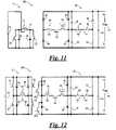
- FIG. 11is a schematic diagram of a DC-DC converter according to an embodiment of the present invention utilizing a push-pull switching converter
- FIG. 12is a schematic diagram of a bidirectional DC-DC converter according to an embodiment of the present invention.
- a voltage converter power stage 10is depicted in FIG. 1 .
- Power stage 10implements a combination of two methods of control, namely variable commutation frequency and PWM.
- a primary portion 12 of power stage 10includes a DC voltage source 14 and a switching converter arrangement comprising four electronic switches, 16 , 18 , 20 , 22 operable as any of a half-bridge, full-bridge or push-pull switching converter.
- Switches 16 - 22may each be any conventional type of electronic switch including, without limitation, field effect transistors, bipolar transistors and solid state relays.
- a free-wheeling diode 24 , 26 , 28 , 30is connected in parallel with each of switches 16 , 18 , 20 , 22 respectively to provide current conduction when an associated switch is off.
- Switches 16 - 22 and diodes 24 - 30function as a full-bridge switching converter to cause an AC current to flow in a primary winding 32 of a step-up transformer 34 .
- Magnetic flux generated in primary winding 32is inductively coupled to a secondary winding 36 of transformer 34 in a secondary portion 38 of power stage 10 .
- a group of rectifiers 40 , 42 , 44 , 46function as a full-wave rectifier to convert the induced AC current of secondary winding 36 to a DC current and voltage.
- Capacitors 48 , 50 , 52 and 54are part of a resonant circuit, discussed in more detail below.
- Capacitor 56filters the DC voltage.
- a first and a second electronic switch, 58 , 60respectively, function as mode-control switches, as discussed more fully below.
- FIG. 2represents one of the possible variants of how the PWM and commutation frequency of primary portion 12 ( FIG. 1 ) may be varied for a given drive level of power stage 10 .
- power stage 10staffs it follows a ramp-up of PWM duty cycle and commutation frequency, depicted as graph lines “A” and “B” respectively in FIG. 2 .
- FIG. 1represents a ramp-up of PWM duty cycle and commutation frequency
- FIG. 2also shows that the commutation frequency and the duty cycle are both varied in response to the amount of load connected to an output of the converter when the power delivered to the load is less than a predetermined threshold level (equating to about 25-35% drive level in this example), and that the commutation frequency is substantially fixed and the duty cycle is varied in response to the amount of load when the power delivered to the load is greater than the predetermined threshold level.
- a predetermined threshold levelequating to about 25-35% drive level in this example
- Secondary portion 38may function in one of two operating modes.
- a first operating modeis a unidirectional resonant converter comprising an inductor 62 and capacitors 48 , 50 , 52 , 54 , with no energy recirculation, and having voltage-doubling rectification provided by diodes 40 , 44 .
- Diodes 42 and 46function as voltage clamps to suppress voltage spikes.
- a second operating modeis a bidirectional resonant converter that provides discharge of the resonant converter, comprising inductor 62 and capacitors 48 , 50 , 52 , 54 , into a load connected to an output 66 of secondary portion 38 .
- the active components switching between the first and second operating modesare switches 58 and 60 , functioning as zero voltage switches (“ZVS.”)
- the other switching componentse.g., switches 16 - 22 and diodes 24 - 30
- the combination of the two control methodsi.e. varying both the commutation frequency and PWM, allows converter power stage 10 to operate with high efficiency.
- Full control of the power delivered at output 66is possible, with a stable output voltage and high stability, and with a rapid response to changes in load (e.g., from no-load to full-load and vice versa), while the input voltage 14 can vary twofold.
- FIG. 3shows a block diagram of a control system 100 for control of converter power stage 10 , depicted in the step-up mode.
- System 100has two independent control loops that are interconnected by a synchronization pulse.
- a first control loopis for the control of the commutation frequency, while the second control loop controls PWM.
- a current transformer 64shown in FIGS. 1 and 3 , is used to provide feedback for control system 100 .
- the frequency control loopconsists of an error amplifier 102 .
- the output of error amplifier 102drives a voltage to a current converter 104 which, in turn, charges a capacitor 106 .
- a comparator 108produces a signal that releases a set pin for a first flip-flop 110 .
- the first signal that arrives at a clock input of flip-flop 110toggles its output. This signal triggers a first timer 112 and a second timer 114 .
- Timer 114discharges capacitor 106 , while the output from timer 112 synchronizes the two control loops.
- the synchronization pulsealso clocks a second flip-flop 116 , which provides the separation of converter power stage 10 ( FIG. 1 ) control pulse into even and odd through a group of AND gates 118 , 120 , 122 and 124 .
- the duration of the pulse from Timer 112preferably equals about half of the minimum commutation period, i.e., the maximum commutation frequency.
- a comparator 126 , a flip-flop 128 , an OR gate 130 and an AND gate 132are provided to reduce the duration of the power conversion cycle to reduce the peak current in the resonant circuit during initial ramp up, i.e., soft start of converter power stage 10 .
- the output capacitor 56 of converter power stage 10is essentially a short circuit, as shown in FIG. 8 .
- a comparator 134 , along with an AND gate 136 , and an OR gate 138provide clamping of the primary side 12 of converter power stage 10 when there is zero current in converter secondary portion 14 , as depicted in FIG. 7 .
- the resolution of the amount of commutation frequency changedepends upon a clock frequency provided by clock 140 , which is preferably at least 4 times the maximum commutation frequency of converter power stage 10 .
- the ultimate commutation frequency change rangepreferably exceeds about 1000:1.
- the PWM control loopincludes a limiter of the maximum/minimum duty cycle of the PWM with a pair of diodes 142 and 144 .
- the minimum limitallows the secondary circuit to function in a resonance mode at the beginning of the power conversion cycle.
- the maximum limitprovides a higher average output current (and hence a lower RMS current) density during the conversion cycle when at high power. This is because the current drop to zero results from inductor 62 energy discharge rather than the resonance process, and thus occurs more quickly.
- the minimum duty cycleis preferably around 10%, and the maximum is preferably around 90%.
- Comparator 146 and AND gate 148produce PWM pulses, synchronized by a pulse from timer 112 by a flip flop 150 and an AND gate 152 , and terminated by the charging of a capacitor 154 .
- a comparator 156 , OR gate 130 , flip-flop 150 , and AND gate 152provide a current limit for the resonant circuit.
- FIG. 4presents waveforms present at various points in control system 100 (see FIG. 3 ) at an intermediate output level (i.e., before maximum commutation frequency is reached).
- FIGS. 5 , 6 , 7 and 8each show converter power stage 10 corresponding to particular times “t” marked on FIG. 4 .
- the present inventionmay be an inverter-charger that converts solar energy to AC.
- the inverter-charger specificationmay be on the order of about 6 kW AC output, with a crest factor of about 5, a maximum commutation frequency of about 150 kHz, a power consumption of about 9-10 watts at idle, and a weak DC-link.
- the present inventionmay be used in step-up topologies for high power application where the output voltage is greater than 200 VDC.
- the converter power stage 10controlled by control system 100 , is characterized by good regulation, rapid transient response, low component stress, high converter efficiency, low EMI emissions, and a relatively low cost as compared to other converters with similar performance metrics.
- FIG. 9is a table of example performance measurements for converters according to embodiments of the present invention, based on an output specifications ranging from about 2-6 kilowatts.
- power stage 10 of FIG. 1is described above utilizing a full-bridge converter on the low-voltage side, the present invention may be applied equally to a “half-bridge” or a “push-pull” configuration on the low-voltage side. This is because the application of the square wave voltage and commutation by the magnetizing current is not fundamentally changed by the differing topologies.
- switches 16 , 18 , 20 , 22 in the full-bridge configurationare operated in a complementary fashion as described above, the half-bridge and the push-pull configurations each require only two complementary switches, as detailed below.
- a power stage 200 utilizing a half-bridge configurationis shown.
- switch 18 and diode 26 of FIG. 1are replaced by a capacitor 202 .
- switch 22 and diode 30 of FIG. 1are replaced by a capacitor 204 .
- Capacitors 202 , 204are each of a suitable capacitance value and voltage rating for power stage 200 .
- about half of the potential of source voltage 14is impressed upon primary 32 when either of switches 16 , 20 is turned on.
- the half-bridge configuration power stage 200requires a greater transformer 34 turns ratio between primary 32 and secondary 36 as compared to the full-bridge power stage 10 of FIG. 1 to achieve a voltage step-up comparable with that of the full-bridge configuration of the power stage. Operation of power stage 200 is the same as power stage 10 ( FIG. 1 ) in all other respects.
- a power stage 300 utilizing a push-pull configurationis shown.
- primary 32 of transformer 34is center tapped.
- the center tapis connected to a positive voltage of voltage source 14 .
- Switches 16 , 18 and diodes 24 , 26 of FIG. 1are removed.
- Switch 20is actuated complementary to switch 22 to generate the magnetizing current in primary 32 .
- Operation of power stage 300is the same as power stage 10 ( FIG. 1 ) in all other respects.
- a power stage 400is depicted.
- Power stage 400is similar to power stage 10 of FIG. 1 , with the addition of a switch 402 connected in parallel with diode 40 and a switch 404 connected in parallel with diode 44 .
- Switches 402 , 404may be any of the previously-discussed types of electronic switches including, but not limited, to an insulated gate bipolar transistor (“IGBT”).
- IGBTinsulated gate bipolar transistor
- Switches 402 , 404may be actuated in a complementary fashion to drive winding 36 of transformer 34 , inductor 62 and capacitors 48 , 50 , 52 , and 54 in a resonant mode. In this way a voltage conversion can be performed, essentially driving transformer 34 in reverse.
- the low voltage power devices 16 , 18 , 20 , and 22can be operated as synchronous rectifiers and diodes 24 , 26 , 28 , and 30 will operate as conventional rectifiers.
- input power from the high voltage side 38is step-down converted to the low voltage side 12 .
- Operation of power stage 400is the same as power stage 10 ( FIG. 1 ) in all other respects.
- the present inventionmay be used to advantage to control various types of voltage converter and inverter topologies.
- a pertinent exampleis the inventors'“Alexander Topology” resonance energy conversion and inversion circuit, disclosed in U.S. Pat. No. 6,483,731, the contents of which are hereby incorporated by reference in its entirety.
Landscapes
- Engineering & Computer Science (AREA)
- Power Engineering (AREA)
- Dc-Dc Converters (AREA)
Abstract
Description
Claims (20)
Priority Applications (1)
| Application Number | Priority Date | Filing Date | Title |
|---|---|---|---|
| US11/035,839US7379309B2 (en) | 2004-01-14 | 2005-01-14 | High-frequency DC-DC converter control |
Applications Claiming Priority (2)
| Application Number | Priority Date | Filing Date | Title |
|---|---|---|---|
| US53632804P | 2004-01-14 | 2004-01-14 | |
| US11/035,839US7379309B2 (en) | 2004-01-14 | 2005-01-14 | High-frequency DC-DC converter control |
Publications (2)
| Publication Number | Publication Date |
|---|---|
| US20050152159A1 US20050152159A1 (en) | 2005-07-14 |
| US7379309B2true US7379309B2 (en) | 2008-05-27 |
Family
ID=34742566
Family Applications (1)
| Application Number | Title | Priority Date | Filing Date |
|---|---|---|---|
| US11/035,839Active2026-03-01US7379309B2 (en) | 2004-01-14 | 2005-01-14 | High-frequency DC-DC converter control |
Country Status (1)
| Country | Link |
|---|---|
| US (1) | US7379309B2 (en) |
Cited By (14)
| Publication number | Priority date | Publication date | Assignee | Title |
|---|---|---|---|---|
| US20080223059A1 (en)* | 2004-09-14 | 2008-09-18 | Ferran Escanes Garcia | Control Method and System |
| WO2012113442A1 (en) | 2011-02-21 | 2012-08-30 | Sma Solar Technology Ag | Dc-to-dc converter and method for operating a dc-to-dc converter |
| US20130099787A1 (en)* | 2011-10-25 | 2013-04-25 | General Electric Company | System and method for series resonant converter protection |
| US20130272032A1 (en)* | 2010-12-02 | 2013-10-17 | Sma Solar Technology Ag | Dc/dc voltage converter and method for operating a dc/dc voltage converter |
| US8811038B2 (en) | 2011-11-11 | 2014-08-19 | Gridco, Inc. | Apparatus and method for soft switching in a medium voltage to low voltage converter |
| CN104811049A (en)* | 2014-01-29 | 2015-07-29 | 艾默生网络能源有限公司 | Resonance circuit |
| US20160020706A1 (en)* | 2013-03-05 | 2016-01-21 | Fronius International Gmbh | Method for controlling an inverter, and inverter |
| US9287795B2 (en) | 2011-10-25 | 2016-03-15 | General Electric Company | System and method for power supply control |
| US9322890B2 (en) | 2011-10-25 | 2016-04-26 | General Electric Company | System and method for gradient amplifier control |
| US20160294221A1 (en)* | 2015-04-05 | 2016-10-06 | Sanjaya Maniktala | Secondary-Side Output Boost Technique in Power Converters and Wireless Power Transfer Systems |
| WO2018040684A1 (en)* | 2016-08-29 | 2018-03-08 | 中兴通讯股份有限公司 | Power circuit, power circuit control method, and storage medium |
| US20180367037A1 (en)* | 2015-12-15 | 2018-12-20 | Safran Electronics & Defense | Switching controller |
| US10396671B2 (en) | 2017-01-20 | 2019-08-27 | Astec International Limited | Power supplies having power switches controllable with a varying frequency, duty cycle and/or phase to regulate outputs |
| US11801763B2 (en) | 2017-12-19 | 2023-10-31 | Ford Global Technologies, Llc | Integrated DC vehicle charger |
Families Citing this family (60)
| Publication number | Priority date | Publication date | Assignee | Title |
|---|---|---|---|---|
| EP1732200A1 (en)* | 2005-06-09 | 2006-12-13 | Koninklijke Philips Electronics N.V. | Method for operating a power converter in a soft-switching range |
| CN1992493B (en)* | 2005-12-30 | 2011-05-18 | 艾默生网络能源系统北美公司 | Resonance DC/DC converter and control method thereof |
| US7660135B2 (en)* | 2007-05-23 | 2010-02-09 | Hamilton Sundstrand Corporation | Universal AC high power inveter with galvanic isolation for linear and non-linear loads |
| US20140185327A1 (en)* | 2012-12-31 | 2014-07-03 | Avogy, Inc | High power density off-line power supply |
| JP6179054B2 (en)* | 2013-07-02 | 2017-08-16 | パナソニックIpマネジメント株式会社 | Bidirectional DC / DC converter, bidirectional power converter |
| US10892140B2 (en) | 2018-07-27 | 2021-01-12 | Eagle Harbor Technologies, Inc. | Nanosecond pulser bias compensation |
| US11539352B2 (en) | 2013-11-14 | 2022-12-27 | Eagle Harbor Technologies, Inc. | Transformer resonant converter |
| US9706630B2 (en) | 2014-02-28 | 2017-07-11 | Eagle Harbor Technologies, Inc. | Galvanically isolated output variable pulse generator disclosure |
| US10978955B2 (en) | 2014-02-28 | 2021-04-13 | Eagle Harbor Technologies, Inc. | Nanosecond pulser bias compensation |
| EP4210223A1 (en) | 2013-11-14 | 2023-07-12 | Eagle Harbor Technologies, Inc. | High voltage nanosecond pulser |
| US11171568B2 (en) | 2017-02-07 | 2021-11-09 | Eagle Harbor Technologies, Inc. | Transformer resonant converter |
| US10020800B2 (en) | 2013-11-14 | 2018-07-10 | Eagle Harbor Technologies, Inc. | High voltage nanosecond pulser with variable pulse width and pulse repetition frequency |
| US10483089B2 (en)* | 2014-02-28 | 2019-11-19 | Eagle Harbor Technologies, Inc. | High voltage resistive output stage circuit |
| CN105024552A (en)* | 2014-04-16 | 2015-11-04 | 艾默生网络能源有限公司 | Resonance circuit, charger and uninterrupted power supply |
| JP6367738B2 (en) | 2015-02-27 | 2018-08-01 | 株式会社日立製作所 | Power converter |
| US9871450B2 (en)* | 2016-04-25 | 2018-01-16 | Vanner, Inc. | Isolated step-up converter |
| US11430635B2 (en) | 2018-07-27 | 2022-08-30 | Eagle Harbor Technologies, Inc. | Precise plasma control system |
| US10903047B2 (en) | 2018-07-27 | 2021-01-26 | Eagle Harbor Technologies, Inc. | Precise plasma control system |
| US11004660B2 (en) | 2018-11-30 | 2021-05-11 | Eagle Harbor Technologies, Inc. | Variable output impedance RF generator |
| CN117200759A (en)* | 2017-03-31 | 2023-12-08 | 鹰港科技有限公司 | High voltage resistive output stage circuit |
| JP6902167B2 (en) | 2017-08-25 | 2021-07-14 | イーグル ハーバー テクノロジーズ, インク.Eagle Harbor Technologies, Inc. | Generation of arbitrary waveforms using nanosecond pulses |
| US10510575B2 (en) | 2017-09-20 | 2019-12-17 | Applied Materials, Inc. | Substrate support with multiple embedded electrodes |
| JP6919759B2 (en)* | 2018-03-07 | 2021-08-18 | 日産自動車株式会社 | Resonant power converter control method, resonant power converter, and DC-DC converter |
| CN110417266A (en) | 2018-04-26 | 2019-11-05 | 比亚迪股份有限公司 | DCDC converters, on-board chargers and electric vehicles |
| US10555412B2 (en) | 2018-05-10 | 2020-02-04 | Applied Materials, Inc. | Method of controlling ion energy distribution using a pulse generator with a current-return output stage |
| CN110504149B (en)* | 2018-05-17 | 2022-04-22 | 北京北方华创微电子装备有限公司 | Pulse modulation system and method of radio frequency power supply |
| US11222767B2 (en) | 2018-07-27 | 2022-01-11 | Eagle Harbor Technologies, Inc. | Nanosecond pulser bias compensation |
| US11302518B2 (en) | 2018-07-27 | 2022-04-12 | Eagle Harbor Technologies, Inc. | Efficient energy recovery in a nanosecond pulser circuit |
| US11810761B2 (en) | 2018-07-27 | 2023-11-07 | Eagle Harbor Technologies, Inc. | Nanosecond pulser ADC system |
| US10607814B2 (en) | 2018-08-10 | 2020-03-31 | Eagle Harbor Technologies, Inc. | High voltage switch with isolated power |
| US11532457B2 (en) | 2018-07-27 | 2022-12-20 | Eagle Harbor Technologies, Inc. | Precise plasma control system |
| JP7038901B2 (en) | 2018-08-10 | 2022-03-18 | イーグル ハーバー テクノロジーズ,インク. | Plasma sheath control for RF plasma reactor |
| US10483862B1 (en) | 2018-10-25 | 2019-11-19 | Vanner, Inc. | Bi-directional isolated DC-DC converter for the electrification of transportation |
| US11476145B2 (en) | 2018-11-20 | 2022-10-18 | Applied Materials, Inc. | Automatic ESC bias compensation when using pulsed DC bias |
| KR20210111841A (en) | 2019-01-08 | 2021-09-13 | 이글 하버 테크놀로지스, 인코포레이티드 | Efficient Energy Recovery in Nanosecond Pulser Circuits |
| KR102827481B1 (en) | 2019-01-22 | 2025-06-30 | 어플라이드 머티어리얼스, 인코포레이티드 | Feedback loop to control pulse voltage waveform |
| US11508554B2 (en) | 2019-01-24 | 2022-11-22 | Applied Materials, Inc. | High voltage filter assembly |
| TWI778449B (en) | 2019-11-15 | 2022-09-21 | 美商鷹港科技股份有限公司 | High voltage pulsing circuit |
| EP4082036B1 (en) | 2019-12-24 | 2025-01-22 | Eagle Harbor Technologies, Inc. | Nanosecond pulser rf isolation for plasma systems |
| US11967484B2 (en) | 2020-07-09 | 2024-04-23 | Eagle Harbor Technologies, Inc. | Ion current droop compensation |
| US11848176B2 (en) | 2020-07-31 | 2023-12-19 | Applied Materials, Inc. | Plasma processing using pulsed-voltage and radio-frequency power |
| US11798790B2 (en) | 2020-11-16 | 2023-10-24 | Applied Materials, Inc. | Apparatus and methods for controlling ion energy distribution |
| US11901157B2 (en) | 2020-11-16 | 2024-02-13 | Applied Materials, Inc. | Apparatus and methods for controlling ion energy distribution |
| US11495470B1 (en) | 2021-04-16 | 2022-11-08 | Applied Materials, Inc. | Method of enhancing etching selectivity using a pulsed plasma |
| US11948780B2 (en) | 2021-05-12 | 2024-04-02 | Applied Materials, Inc. | Automatic electrostatic chuck bias compensation during plasma processing |
| US11791138B2 (en) | 2021-05-12 | 2023-10-17 | Applied Materials, Inc. | Automatic electrostatic chuck bias compensation during plasma processing |
| US11967483B2 (en) | 2021-06-02 | 2024-04-23 | Applied Materials, Inc. | Plasma excitation with ion energy control |
| US12394596B2 (en) | 2021-06-09 | 2025-08-19 | Applied Materials, Inc. | Plasma uniformity control in pulsed DC plasma chamber |
| US20220399185A1 (en) | 2021-06-09 | 2022-12-15 | Applied Materials, Inc. | Plasma chamber and chamber component cleaning methods |
| US11810760B2 (en) | 2021-06-16 | 2023-11-07 | Applied Materials, Inc. | Apparatus and method of ion current compensation |
| US11569066B2 (en) | 2021-06-23 | 2023-01-31 | Applied Materials, Inc. | Pulsed voltage source for plasma processing applications |
| US11476090B1 (en) | 2021-08-24 | 2022-10-18 | Applied Materials, Inc. | Voltage pulse time-domain multiplexing |
| US12106938B2 (en) | 2021-09-14 | 2024-10-01 | Applied Materials, Inc. | Distortion current mitigation in a radio frequency plasma processing chamber |
| WO2023073584A1 (en)* | 2021-10-27 | 2023-05-04 | Elan Future Inc. | System and method for managing power delivery to a load |
| US11972924B2 (en) | 2022-06-08 | 2024-04-30 | Applied Materials, Inc. | Pulsed voltage source for plasma processing applications |
| US12315732B2 (en) | 2022-06-10 | 2025-05-27 | Applied Materials, Inc. | Method and apparatus for etching a semiconductor substrate in a plasma etch chamber |
| US11824542B1 (en) | 2022-06-29 | 2023-11-21 | Eagle Harbor Technologies, Inc. | Bipolar high voltage pulser |
| US12272524B2 (en) | 2022-09-19 | 2025-04-08 | Applied Materials, Inc. | Wideband variable impedance load for high volume manufacturing qualification and on-site diagnostics |
| KR20250084155A (en) | 2022-09-29 | 2025-06-10 | 이글 하버 테크놀로지스, 인코포레이티드 | High voltage plasma control |
| US12111341B2 (en) | 2022-10-05 | 2024-10-08 | Applied Materials, Inc. | In-situ electric field detection method and apparatus |
Citations (11)
| Publication number | Priority date | Publication date | Assignee | Title |
|---|---|---|---|---|
| US4317165A (en) | 1980-06-17 | 1982-02-23 | Vanner, Inc. | Inverter having improved efficiency and regulation |
| US4855888A (en) | 1988-10-19 | 1989-08-08 | Unisys Corporation | Constant frequency resonant power converter with zero voltage switching |
| US4975823A (en)* | 1987-09-30 | 1990-12-04 | Deutsche Thomson-Brandt Gmbh | Switched power supply with current mode regulation |
| US5157593A (en) | 1990-12-13 | 1992-10-20 | Northern Telecom Limited | Constant frequency resonant dc/dc converter |
| US5325283A (en)* | 1992-06-08 | 1994-06-28 | Center For Innovative Technology | Novel zero-voltage-switching family of isolated converters |
| US5373196A (en) | 1992-10-16 | 1994-12-13 | Vanner Weldon Inc. | Combination static/dynamic inverter |
| US5452197A (en) | 1993-02-04 | 1995-09-19 | Vanner Weldon, Inc. | Static DC to AC power converter including separate high and low power converters |
| US5539630A (en)* | 1993-11-15 | 1996-07-23 | California Institute Of Technology | Soft-switching converter DC-to-DC isolated with voltage bidirectional switches on the secondary side of an isolation transformer |
| US5777864A (en) | 1995-12-28 | 1998-07-07 | Samsung Electronics Co., Ltd. | Resonant converter control system having resonant current phase detection |
| US6154375A (en) | 1999-10-08 | 2000-11-28 | Philips Electronics North America Corporation | Soft start scheme for resonant converters having variable frequency control |
| US6483731B1 (en) | 2000-07-31 | 2002-11-19 | Vanner, Inc. | Alexander topology resonance energy conversion and inversion circuit utilizing a series capacitance multi-voltage resonance section |
- 2005
- 2005-01-14USUS11/035,839patent/US7379309B2/enactiveActive
Patent Citations (11)
| Publication number | Priority date | Publication date | Assignee | Title |
|---|---|---|---|---|
| US4317165A (en) | 1980-06-17 | 1982-02-23 | Vanner, Inc. | Inverter having improved efficiency and regulation |
| US4975823A (en)* | 1987-09-30 | 1990-12-04 | Deutsche Thomson-Brandt Gmbh | Switched power supply with current mode regulation |
| US4855888A (en) | 1988-10-19 | 1989-08-08 | Unisys Corporation | Constant frequency resonant power converter with zero voltage switching |
| US5157593A (en) | 1990-12-13 | 1992-10-20 | Northern Telecom Limited | Constant frequency resonant dc/dc converter |
| US5325283A (en)* | 1992-06-08 | 1994-06-28 | Center For Innovative Technology | Novel zero-voltage-switching family of isolated converters |
| US5373196A (en) | 1992-10-16 | 1994-12-13 | Vanner Weldon Inc. | Combination static/dynamic inverter |
| US5452197A (en) | 1993-02-04 | 1995-09-19 | Vanner Weldon, Inc. | Static DC to AC power converter including separate high and low power converters |
| US5539630A (en)* | 1993-11-15 | 1996-07-23 | California Institute Of Technology | Soft-switching converter DC-to-DC isolated with voltage bidirectional switches on the secondary side of an isolation transformer |
| US5777864A (en) | 1995-12-28 | 1998-07-07 | Samsung Electronics Co., Ltd. | Resonant converter control system having resonant current phase detection |
| US6154375A (en) | 1999-10-08 | 2000-11-28 | Philips Electronics North America Corporation | Soft start scheme for resonant converters having variable frequency control |
| US6483731B1 (en) | 2000-07-31 | 2002-11-19 | Vanner, Inc. | Alexander topology resonance energy conversion and inversion circuit utilizing a series capacitance multi-voltage resonance section |
Non-Patent Citations (10)
| Title |
|---|
| A. Isurin, A.Cook, A Novel Resonant Converter Topology and its Application, IEEE Power Electronics Specialists Conference, PESC 2001, vol. 2, pp. 1039-1044, Vancouver, BC, Canada, Jun. 2001. |
| G. C. Hsieh, C. H. Lin, J. M. Li, Y. C. Hsu, A Study of Series-Resonant DC/AC Inverter, IEEE Transactions on Power Electronics, vol. 11, No. 4, Jul. 1996, pp. 641-652. |
| G. S. N. Raju, S. Doralda, An LCL Resonant Converter with PWM Control-Analysis, Simulation, and Implementation, IEEE Transactions on Power Electronics, vol. 10, No. 2, Mar. 1995, pp. 164-173. |
| H. Li, F.Z. Peng, J. Lawler, Modeling, Simulation, and Experimental Verification of Soft-Switched Bi-Directional DC-DC Converters, IEEE Applied Power Electronics Conference and Exposition, APEC 2001, vol. 2, pp. 736-744, Anaheim, CA, Mar. 2001, no month. |
| I. Batarseh, Resonant Converter Topologies with Three and Four Energy Storage Elements, IEEE Transactions on Power Electronics, vol. 9, No. 1, Jan. 1994, pp. 64-73. |
| J. L. Lin, J. S. Lew, Robust Controller Design for a Series Resonant Converter Via Duty-Cycle Control, IEEE Transactions on Power Electronics, vol. 14, No. 5, Sep. 1999, pp. 793-801. |
| M. Ishida, H. Fujino, T. Hori, Real-Time Output Voltage Control Method of Quasi-ZCS Series Resonant HF-Linked DC-AC Converter, IEEE Transactions on Power Electronics, vol. 10, No. 6, Nov. 1995, pp. 776-783. |
| N.H. Li, F.Z. Peng, J.S. Lawer, A Natural ZVS Medium-Power Bidirectional DC-DC Converter With Minimum Number of Devices, IEEE Transactions on Industry Applications, vol. 39, No. 2, Mar./Apr. 2003, pp. 525-535. |
| O. Q. Zhao, Fred C. Lee, High-Efficiency, High Step-Up DC-DC Converters, IEEE Transactions on Power Electronics, vol. 18, No. 1, Jan. 2003, pp. 65-73. |
| R. Oruganti, P.C. Heng, J.T.K. Guan, L. A. Choy, Soft-Switched DC/DC Converter with PWM Control, IEEE Transactions on Power Electronics, vol. 13, No. 1, Jan. 1998, pp. 102-113. |
Cited By (19)
| Publication number | Priority date | Publication date | Assignee | Title |
|---|---|---|---|---|
| US8087259B2 (en)* | 2004-09-14 | 2012-01-03 | Appliances Components Companies Spain, S.A. | Control method and system |
| US20080223059A1 (en)* | 2004-09-14 | 2008-09-18 | Ferran Escanes Garcia | Control Method and System |
| US20130272032A1 (en)* | 2010-12-02 | 2013-10-17 | Sma Solar Technology Ag | Dc/dc voltage converter and method for operating a dc/dc voltage converter |
| WO2012113442A1 (en) | 2011-02-21 | 2012-08-30 | Sma Solar Technology Ag | Dc-to-dc converter and method for operating a dc-to-dc converter |
| US9287795B2 (en) | 2011-10-25 | 2016-03-15 | General Electric Company | System and method for power supply control |
| US20130099787A1 (en)* | 2011-10-25 | 2013-04-25 | General Electric Company | System and method for series resonant converter protection |
| US9322890B2 (en) | 2011-10-25 | 2016-04-26 | General Electric Company | System and method for gradient amplifier control |
| US9425700B2 (en)* | 2011-10-25 | 2016-08-23 | General Electric Company | System and method for series resonant converter protection |
| US8811038B2 (en) | 2011-11-11 | 2014-08-19 | Gridco, Inc. | Apparatus and method for soft switching in a medium voltage to low voltage converter |
| US9812988B2 (en)* | 2013-03-05 | 2017-11-07 | Fronius International Gmbh | Method for controlling an inverter, and inverter |
| US20160020706A1 (en)* | 2013-03-05 | 2016-01-21 | Fronius International Gmbh | Method for controlling an inverter, and inverter |
| CN104811049A (en)* | 2014-01-29 | 2015-07-29 | 艾默生网络能源有限公司 | Resonance circuit |
| US20160294221A1 (en)* | 2015-04-05 | 2016-10-06 | Sanjaya Maniktala | Secondary-Side Output Boost Technique in Power Converters and Wireless Power Transfer Systems |
| US10923952B2 (en)* | 2015-04-05 | 2021-02-16 | Chargedge, Inc. | Secondary-side output boost technique in power converters and wireless power transfer systems |
| US20180367037A1 (en)* | 2015-12-15 | 2018-12-20 | Safran Electronics & Defense | Switching controller |
| US10250140B2 (en)* | 2015-12-15 | 2019-04-02 | Safran Electronics & Defense | Switching controller |
| WO2018040684A1 (en)* | 2016-08-29 | 2018-03-08 | 中兴通讯股份有限公司 | Power circuit, power circuit control method, and storage medium |
| US10396671B2 (en) | 2017-01-20 | 2019-08-27 | Astec International Limited | Power supplies having power switches controllable with a varying frequency, duty cycle and/or phase to regulate outputs |
| US11801763B2 (en) | 2017-12-19 | 2023-10-31 | Ford Global Technologies, Llc | Integrated DC vehicle charger |
Also Published As
| Publication number | Publication date |
|---|---|
| US20050152159A1 (en) | 2005-07-14 |
Similar Documents
| Publication | Publication Date | Title |
|---|---|---|
| US7379309B2 (en) | High-frequency DC-DC converter control | |
| US10135350B2 (en) | AC/DC converters with wider voltage regulation range | |
| US10833594B2 (en) | System and method of controlling a power converter having an LC tank coupled between a switching network and a transformer winding | |
| US9263960B2 (en) | Power converters for wide input or output voltage range and control methods thereof | |
| US7596007B2 (en) | Multiphase DC to DC converter | |
| Wang | A novel ZCS-PWM flyback converter with a simple ZCS-PWM commutation cell | |
| US7869237B1 (en) | Phase-shifted bridge with auxiliary circuit to maintain zero-voltage-switching | |
| US8842450B2 (en) | Power converter using multiple phase-shifting quasi-resonant converters | |
| Oruganti et al. | Soft-switched DC/DC converter with PWM control | |
| JP3344356B2 (en) | Switching power supply | |
| US6906931B1 (en) | Zero-voltage switching half-bridge DC-DC converter topology by utilizing the transformer leakage inductance trapped energy | |
| WO2005101635A1 (en) | Soft-switching power converter having power saving means | |
| US7400061B2 (en) | Soft switched secondary side post regulator for DC to DC converter | |
| Awasthi et al. | Time-domain analysis of APWM-frequency modulated low-Q LLC resonant converter for wide input and load range applications | |
| Zhao et al. | Efficiency improvement of an adaptive-energy-storage full-bridge converter by modifying turns ratio of a coupled inductor | |
| US8023295B1 (en) | Direct current (DC) to alternating current (AC) generation | |
| Shahzad et al. | LLC series resonant converter with PID controller for battery charging application | |
| JP5418910B2 (en) | DC-DC converter | |
| Qian | An adaptive current injection scheme for resonant capacitor of LLC resonant converters with suppressed frequency variation | |
| Awasthi et al. | Variable frequency-duty cycle modulation technique for light load efficiency improvement of LLC resonant converter for wide input voltage range in PV applications | |
| Moosavi et al. | Soft-switching push-pull converter with parallel resonant link and buck-boost capability | |
| Fernández et al. | Low output voltage AC/DC converter with a new scheme of synchronous rectification that complies with IEC 1000-3-2 regulations | |
| Li et al. | Multimode LLC resonant DC− DC converters for wide range input voltage | |
| Chen et al. | A novel soft-switching full-bridge converter for ZVS in light and full load conditions with current-doubler rectifier | |
| Junglas et al. | Modulation Strategy for a HV-DAB driving DE Transducers considering Resonant Transitions |
Legal Events
| Date | Code | Title | Description |
|---|---|---|---|
| AS | Assignment | Owner name:VANNER, INC., OHIO Free format text:ASSIGNMENT OF ASSIGNORS INTEREST;ASSIGNORS:ISURIN, ALEXANDER;COOK, ALEXANDER;REEL/FRAME:016683/0657 Effective date:20050114 | |
| STCF | Information on status: patent grant | Free format text:PATENTED CASE | |
| CC | Certificate of correction | ||
| FEPP | Fee payment procedure | Free format text:PAT HOLDER CLAIMS SMALL ENTITY STATUS, ENTITY STATUS SET TO SMALL (ORIGINAL EVENT CODE: LTOS); ENTITY STATUS OF PATENT OWNER: SMALL ENTITY | |
| FPAY | Fee payment | Year of fee payment:4 | |
| AS | Assignment | Owner name:JPMORGAN CHASE BANK, N.A., OHIO Free format text:SECURITY AGREEMENT;ASSIGNORS:VANNER, INC.;VANNER HOLDINGS, INC.;REEL/FRAME:032366/0220 Effective date:20140227 | |
| AS | Assignment | Owner name:THE HUNTINGTON CAPITAL INVESTMENT COMPANY II, OHIO Free format text:SECURITY INTEREST;ASSIGNORS:VANNER, INC.;VANNER PARTNERS HOLDINGS, LLC;VANNER HOLDINGS, INC.;REEL/FRAME:032643/0196 Effective date:20140228 | |
| AS | Assignment | Owner name:VANNER HOLDINGS, INC., OHIO Free format text:RELEASE BY SECURED PARTY;ASSIGNOR:HUNTINGTON CAPITAL INVESTMENT COMPANY II;REEL/FRAME:036720/0177 Effective date:20150930 Owner name:VHI HOLDING, INC., OHIO Free format text:RELEASE BY SECURED PARTY;ASSIGNOR:HUNTINGTON CAPITAL INVESTMENT COMPANY II;REEL/FRAME:036720/0177 Effective date:20150930 Owner name:VANNER, INC., OHIO Free format text:RELEASE BY SECURED PARTY;ASSIGNOR:HUNTINGTON CAPITAL INVESTMENT COMPANY II;REEL/FRAME:036720/0177 Effective date:20150930 Owner name:VANNER PARTNERS HOLDING, LLC, OHIO Free format text:RELEASE BY SECURED PARTY;ASSIGNOR:HUNTINGTON CAPITAL INVESTMENT COMPANY II;REEL/FRAME:036720/0177 Effective date:20150930 | |
| AS | Assignment | Owner name:VANNER, INC., OHIO Free format text:RELEASE BY SECURED PARTY;ASSIGNOR:JPMORGAN CHASE BANK, N.A.;REEL/FRAME:036748/0982 Effective date:20151001 Owner name:VANNER HOLDINGS, INC., OHIO Free format text:RELEASE BY SECURED PARTY;ASSIGNOR:JPMORGAN CHASE BANK, N.A.;REEL/FRAME:036748/0982 Effective date:20151001 | |
| FPAY | Fee payment | Year of fee payment:8 | |
| MAFP | Maintenance fee payment | Free format text:PAYMENT OF MAINTENANCE FEE, 12TH YR, SMALL ENTITY (ORIGINAL EVENT CODE: M2553); ENTITY STATUS OF PATENT OWNER: SMALL ENTITY Year of fee payment:12 | |
| AS | Assignment | Owner name:CIBC BANK USA, ILLINOIS Free format text:SECURITY INTEREST;ASSIGNOR:VANNER, INC.;REEL/FRAME:066339/0698 Effective date:20240201 | |
| AS | Assignment | Owner name:THE HUNTINGTON NATIONAL BANK, AS ADMINISTRATIVE AGENT, OHIO Free format text:SECURITY INTEREST;ASSIGNORS:HAVIS, INC.;VANNER, INC.;ENGINEERED NETWORK SYSTEMS, LLC;REEL/FRAME:068132/0552 Effective date:20240730 | |
| AS | Assignment | Owner name:VANNER, INC., OHIO Free format text:RELEASE BY SECURED PARTY;ASSIGNOR:CIBC BANK USA, AS ADMINISTRATIVE AGENT;REEL/FRAME:068149/0745 Effective date:20240730 | |
| AS | Assignment | Owner name:HAVIS, INC., PENNSYLVANIA Free format text:ASSIGNMENT OF ASSIGNORS INTEREST;ASSIGNOR:VANNER INC.,;REEL/FRAME:069444/0476 Effective date:20241122 |