US7379163B2 - Method and system for automatic gain control of sensors in time-of-flight systems - Google Patents
Method and system for automatic gain control of sensors in time-of-flight systemsDownload PDFInfo
- Publication number
- US7379163B2 US7379163B2US11/349,310US34931006AUS7379163B2US 7379163 B2US7379163 B2US 7379163B2US 34931006 AUS34931006 AUS 34931006AUS 7379163 B2US7379163 B2US 7379163B2
- Authority
- US
- United States
- Prior art keywords
- optical energy
- emitted optical
- pixel
- pixel photodetectors
- receiving
- Prior art date
- Legal status (The legal status is an assumption and is not a legal conclusion. Google has not performed a legal analysis and makes no representation as to the accuracy of the status listed.)
- Expired - Fee Related, expires
Links
- 238000000034methodMethods0.000titleclaimsdescription28
- 230000008859changeEffects0.000claimsabstractdescription12
- 230000003287optical effectEffects0.000claimsdescription109
- 238000001514detection methodMethods0.000claimsdescription46
- 230000010354integrationEffects0.000claimsdescription18
- 230000000737periodic effectEffects0.000claimsdescription12
- 238000002310reflectometryMethods0.000claimsdescription4
- 238000005286illuminationMethods0.000claims2
- 238000003384imaging methodMethods0.000abstractdescription9
- 238000013139quantizationMethods0.000abstract1
- 238000005259measurementMethods0.000description21
- 230000006870functionEffects0.000description13
- 230000010363phase shiftEffects0.000description7
- 238000012545processingMethods0.000description7
- 239000003990capacitorSubstances0.000description4
- 230000007246mechanismEffects0.000description4
- 238000006243chemical reactionMethods0.000description3
- 230000008569processEffects0.000description3
- 230000008901benefitEffects0.000description2
- 238000004590computer programMethods0.000description2
- 230000003247decreasing effectEffects0.000description2
- 238000010586diagramMethods0.000description2
- OKTJSMMVPCPJKN-UHFFFAOYSA-NCarbonChemical compound[C]OKTJSMMVPCPJKN-UHFFFAOYSA-N0.000description1
- 238000005481NMR spectroscopyMethods0.000description1
- 210000004556brainAnatomy0.000description1
- 238000004422calculation algorithmMethods0.000description1
- 238000004364calculation methodMethods0.000description1
- 230000001447compensatory effectEffects0.000description1
- 238000012937correctionMethods0.000description1
- 230000003111delayed effectEffects0.000description1
- 230000001771impaired effectEffects0.000description1
- 239000000463materialSubstances0.000description1
- 238000012986modificationMethods0.000description1
- 230000004048modificationEffects0.000description1
- 210000000056organAnatomy0.000description1
- 230000005855radiationEffects0.000description1
- 230000009467reductionEffects0.000description1
- 238000009877renderingMethods0.000description1
- 230000004044responseEffects0.000description1
- 238000009738saturatingMethods0.000description1
- 238000000926separation methodMethods0.000description1
- 238000003325tomographyMethods0.000description1
- 238000012876topographyMethods0.000description1
- 230000000007visual effectEffects0.000description1
- 238000003466weldingMethods0.000description1
Images


Classifications
- G—PHYSICS
- G01—MEASURING; TESTING
- G01C—MEASURING DISTANCES, LEVELS OR BEARINGS; SURVEYING; NAVIGATION; GYROSCOPIC INSTRUMENTS; PHOTOGRAMMETRY OR VIDEOGRAMMETRY
- G01C3/00—Measuring distances in line of sight; Optical rangefinders
- G01C3/02—Details
- G01C3/06—Use of electric means to obtain final indication
- G01C3/08—Use of electric radiation detectors
Definitions
- the inventionrelates generally to CMOS-implementable image sensors suitable for time-of-flight three-dimensional applications including range and camera sensors, and more specifically to dynamically varying at least one TOF system parameter to maximize the number of photodetector sensors operating within their intended dynamic range. In this fashion, more reliable depth measurement data is obtained from a greater number of pixel photodiode sensors.
- Electronic camera and range sensor systemsthat provide a measure of distance z from the system to a target object are known in the art. Many such systems approximate the range to the target object based upon luminosity or brightness information obtained from the target object. Some such systems are passive and respond to ambient light reflected from the target object, while other systems emit and then detect emitted light reflected from the target object. However brightness or luminosity-based systems may erroneously yield the same measurement information for a distant target object that may be large with a shiny surface and is thus highly reflective, as for a smaller target object that is closer to the system but has a dull surface that is less reflective.
- range finder autofocus camerasemploy detectors to approximate average distance from the camera to the target object by examining relative luminosity (brightness) data obtained from the object.
- the field of viewis sufficiently small such that all objects in focus will be at substantially the same distance. But in general, luminosity-based systems do not work well and are subject to error, as noted above.
- Some cameras and binocularsemploy active infrared ( 1 R) autofocus systems that produce a single distance value that is an average or a minimum distance to all targets within the field of view.
- Other camera autofocus systemsoften require mechanical focusing of the lens onto the subject to determine distance.
- these prior art focus systemscan focus a lens onto a single object in a field of view, but cannot simultaneously measure distance for all objects in the field of view.
- a reproduction or approximation of original luminosity values in a scenepermits the human visual system to understand what objects were present in the scene and to estimate their relative locations stereoscopically.
- the human brainassesses apparent size, distance and shape of objects using past experience.
- Specialized computer programscan approximate object distance under special conditions.
- Stereoscopic imagesallow a human observer to more accurately judge the distance of an object. However it is challenging for a computer program to judge object distance from a stereoscopic image. Errors are often present, and the required signal processing requires specialized hardware and computation. Stereoscopic images are at best an indirect way to produce a three-dimensional image suitable for direct computer use.
- scanning laser range finding systemsraster scan an image by using mirrors to deflect a laser beam in the x-axis and perhaps the y-axis plane.
- the angle of deflection of each mirroris used to determine the coordinate of an image pixel being sampled.
- Such systemsrequire precision detection of the angle of each mirror to determine which pixel is currently being sampled. Understandably having to provide precision moving mechanical parts add bulk, complexity, and cost to such range finding system. Further, because these systems sample each pixel sequentially, the number of complete image frames that can be sampled per unit time is limited.
- pixelcan refer to an output result produced from one or more detectors in an array of detectors.
- pixelcan refer to an output result produced from one or more detectors in an array of detectors.
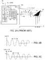
- FIG. 1depicts an exemplary TOF system, as described in U.S. Pat. No. 6,323,942 entitled CMOS-Compatible Three-Dimensional Image Sensor IC (2001), which patent is incorporated herein by reference as further background material.
- TOF system 100can be implemented on a single IC 110 , without moving parts and with relatively few off-chip components.
- System 100includes a two-dimensional array 130 of pixel detectors 140 , each of which has dedicated circuitry 150 for processing detection charge output by the associated detector.
- array 130might include 100 ⁇ 100 pixels 230 , and thus include 100 ⁇ 100 processing circuits 150 .
- IC 110also includes a microprocessor or microcontroller unit 160 , memory 170 (which preferably includes random access memory or RAM and read-only memory or ROM), a high speed distributable clock 180 , and various computing and input/output (I/O) circuitry 190 .
- I/O circuitry 190includes functions such as analog-to-digital (A/D) conversion of the output signals from the pixel photodetectors in array 130 , and system video gain.
- controller unit 160may perform distance to object and object velocity calculations.
- a source of optical energy 120is periodically energized and emits optical energy via lens 125 toward an object target 20 .
- the optical energyis light, for example emitted by a laser diode or LED device 120 .
- Some of the emitted optical energywill be reflected off the surface of target object 20 , and will pass through an aperture field stop and lens, collectively 135 , and will fall upon two-dimensional array 130 of pixel detectors 140 where an image is formed.
- Each imaging pixel detector 140measures both intensity or amplitude of the optical energy received, and the phase-shift of the optical energy as it travels from emitter 120 , through distance Z to target object 20 , and then distance again back to imaging sensor array 130 .
- For each pulse of optical energy transmitted by emitter 120a three-dimensional image of the visible portion of target object 20 is acquired.
- Emitted optical energy traversing to more distant surface regions of target object 20 before being reflected back toward system 100will define a longer time-of-flight than radiation falling upon and being reflected from a nearer surface portion of the target object (or a closer target object).
- a TOF sensor systemcan acquire three-dimensional images of a target object in real time. Such systems advantageously can simultaneously acquire both luminosity data (e.g., signal amplitude) and true TOF distance measurements of a target object or scene.
- each pixel detector 140has an associated high speed counter that accumulates clock pulses in a number directly proportional to TOF for a system-emitted pulse to reflect from an object point and be detected by a pixel detector focused upon that point.
- the TOF dataprovides a direct digital measure of distance from the particular pixel to a point on the object reflecting the emitted pulse of optical energy.
- each pixel detector 140is provided with a charge accumulator and an electronic shutter. The shutters are opened when a pulse of optical energy is emitted, and closed thereafter such that each pixel detector accumulates charge as a function of return photon energy falling upon the associated pixel detector. The amount of accumulated charge provides a direct measure of round-trip TOF.
- TOF datapermits reconstruction of the three-dimensional topography of the light-reflecting surface of the object being imaged.
- array 130may comprise an array of charge-coupled devices (CCDs) or CMOS devices.
- CCDstypically are configured in a so-called bucket-brigade whereby light-detected charge by a first CCD is serial-coupled to an adjacent CCD, whose output in turn is coupled to a third CCD, and so on.
- Bucket-brigade configurationsgenerally preclude fabricating processing circuitry on the same IC containing the CCD array. Further, CCDs provide a serial readout as opposed to a random readout.
- CCD range finder systemFor example, if a CCD range finder system were used in a digital zoom lens application, even though most of the relevant data would be provided by a few of the CCDs in the array, it would nonetheless be necessary to readout the entire array to gain access to the relevant data, a time consuming process. In still and some motion photography applications, CCD-based systems might still find utility.
- the transmitted optical energymay be emitted multiple times using different systems settings to increase reliability of the acquired TOF measurements.
- the initial phase of the emitted optical energymight be varied to cope with various ambient and reflectivity conditions.
- the amplitude of the emitted energymight be varied to increase system dynamic range.
- the exposure duration of the emitted optical energymay be varied to increase dynamic range of the system.
- frequency of the emitted optical energymay be varied to improve the unambiguous range of the system measurements.
- U.S. Pat. No. 6,580,496 entitled Systems for CMOS-Compatible Three-Dimensional Image-Sensing Using Quantum Efficiency Modulationdiscloses a sophisticated system in which relative phase ( ⁇ ) shift between the transmitted light signals and signals reflected from the target object is examined to acquire distance z.
- ⁇relative phase
- Detection of the reflected light signals over multiple locations in a pixel arrayresults in measurement signals that are referred to as depth images.
- FIG. 2Adepicts a system 100 ′ according to the '496 patent, in which an oscillator 115 is controllable by microprocessor 160 to emit high frequency (perhaps 200 MHz) component periodic signals, ideally representable as A ⁇ cos( ⁇ t).
- Emitter 120transmitted optical energy having low average and peak power in the tens of mW range, which emitted signals permitted use of inexpensive light sources and simpler, narrower bandwidth (e.g., a few hundred KHz) pixel detectors 140 ′.
- elements in FIG. 2A with like reference numerals to elements in FIG. 1may be similar or identical elements.
- detection current output by individual pixel detector sensorswas directly integrated and collected using an integration capacitor to develop a detection voltage signal.
- the integrated detection voltage signalwas compared to a threshold voltage and whenever the threshold voltage was exceeded, the capacitor was reset, and the number of resets was stored. In this fashion, the total change in detection voltage could be measured, and dynamic range could be extended by virtue of the resets.
- U.S. Pat. No. 6,919,549before start of integration, a fixed potential was imposed upon each capacitor.
- the potential across each capacitorcould be reset before the integration detection voltage signal reach saturation, or overload, levels. Again the total change in detection voltage could be measured and dynamic range could be extended by virtue of the pre-integration voltage and resets.
- the sensors in many of these embodimentswere operable in differential mode, to better reject common mode signals such as ambient light.
- sensor performancemay be impaired by many parameters. Some or all sensors may not receive sufficient optical energy to perform well, in which case a reliable measurement of depth z cannot be obtained. Similarly, some or all sensors may receive too much optical energy, in which case the sensors may overload and saturate, with the result that a reliable measurement of depth z cannot be obtained. It is when a sensor receives an amount of optical energy within the dynamic range of the sensor that an accurate sensor output signal is provided, and reliable measurements of depth z can be obtained.
- a mechanism for use with pixel detector sensors in a CMOS three-dimensional TOF systemto maximize the number of sensors that are operating within their dynamic range.
- a mechanism for use with pixel detector sensors in a CMOS three-dimensional TOF systemshould function dynamically such that as system parameters that affect sensor performance change, appropriate compensating changes or corrections to individual pixel detector sensors can be made.
- the desired resultis that more valid z-depth measurement data will be provided despite variations in such system parameters.
- the present inventionprovides a method and sub-system to dynamically provide compensating changes to pixel detector sensors such that more valid z depth measurement data will be provided, despite changes in system parameters that would otherwise impair more of the z depth measurement data.
- the present inventionis preferably practiced with a TOF system that acquires phase information to determine z depth measurement data.
- the present inventiondynamically controls at least one parameter of the TOF system such that a greatest number of individual pixel photodiode detector sensors operate within their dynamic range.
- Detection datais acquired representing active optical energy, e.g., detection responsive to optical energy emitted by the TOF system, e.g., modulated energy
- detection datais acquired representing passive or ambient optical energy that is unmodulated, e.g., detection when no optical energy has been emitted by the TOF system.
- the present inventionexamines four phases of detected signals, after which the passive brightness mode (e.g., ambient light) amplitude component of the detected signals is examined. If brightness data indicate sensor saturation at present (e.g., ambient optical energy is too high for the pixel photodetectors to detect within their dynamic range), then the present invention commands one or more compensatory parameters in the TOF system, for example varying the number of common mode resets, varying the signal integration time, varying system gain, etc.
- An objectis to maximize the number of pixel photodetectors that are operating within their intended dynamic range, and thus can output accurate depth data. More specifically, in one embodiment a histogram is calculated using active mode brightness mode.
- the present inventionfirst compensates the TOF sensors by varying common mode resets to accommodate passive optical energy levels, and then to compensate for active optical energy levels.
- Embodiments of the present inventioncan also adjust common mode resets, system parameters including integration time and video gain. These adjustments may be in addition to or in lieu of common mode reset adjustments. Implementation of the present invention maximizes the number of pixel detector sensors in the sensor array that output valid depth measurements.
- FIG. 1is a diagram showing a generic luminosity-based range finding system, according to the prior art
- FIG. 2Adepicts a phase-shift intensity and range finding system, according to the prior art
- FIG. 2Bdepicts a transmitted periodic signal with high frequency components transmitted by the system of FIG. 2A , according to the prior art
- FIG. 2Cdepicts the return waveform with phase-delay for the transmitted signal of FIG. 2B , according to the prior art
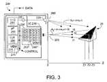
- FIG. 3is a block diagram of a preferred phase-shift system implementation useable with embodiments of the present invention.
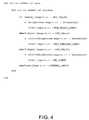
- FIG. 4depicts exemplary pseudocode by which following traversal of depth, brightness, and active brightness images, pixel detectors are assigned to one of several quantized groups depending upon amount of active optical energy seen by each pixel detector, according to an embodiment of the present invention
- FIG. 5depicts exemplary pseudocode by which corrective command(s) are determined as needed to vary at least one TOF system parameter to maximize number of pixel detectors operating within their intended detector dynamic range, according to an embodiment of the present invention
- FIG. 6depicts exemplary pseudocode by which a histogram of all pixel detectors is generated for active brightness and passive brightness images, after which an estimation function is determined, and corrective command(s) are determined as needed to vary at least one TOF system parameter to maximize number of pixel detectors operating within their intended dynamic range, according to an embodiment of the present invention.
- FIG. 3depicts a TOF system 200 with which the present invention, denoted 275 , may be practiced to improve the validity of z depth measurements output as DATA.
- Element 275preferably is software that when executed by microprocessor 260 carries out method steps, exemplified by the pseudocode of FIGS. 4-6 .
- the present inventionmaximizes the number of photodetector pixels 240 ′′′ in array 230 that operate within their intended dynamic range.
- the present inventioncan exercise control (depicted in FIG. 3 as CONTROL) over at least one parameter of TOF system 200 . For example, if the present invention determines that too many photodetectors are saturating, a CONTROL signal can be generated varying at least one TOF system 200 parameter.
- the CONTROL signalmay cause TOF system 200 to more frequently reset common mode in the detectors, as described in U.S. Pat. No. 6,919,549 (2005) Method and System to Differentially Enhance Sensor Dynamic Range, and/or to reduce detection integration or exposure time, and/or to reduce video or detection system gain.
- the CONTROL signal generated by the present inventioncan vary at least one TOF system 200 parameter in the opposite direction, e.g., to reduce the number of common mode resets in the detectors, to increase detection integration or exposure time, to increase detector and/or video gain.
- the present inventiondynamically and automatically varies at least one TOF system parameter such that at any given time, a maximum number of photodetector pixels are responded to optical energy within their intended dynamic range.
- system 200includes a driver 215 , preferably commanded by microprocessor 260 that drives optical light source or emitter 220 .
- An exemplary emitter 220may be a low peak power laser diode, or low peak power LED, that can output a periodic signal with 50 mW or so peak power when driven with a repetition rate of a few hundred MHz and, in the preferred embodiment, a duty cycle close to 100%, as duty cycle is defined herein.
- Emitted optical energymay have an exemplary wavelength of perhaps 800 nm.
- a lens 285 ′is used to focus the optical light energy transmitted from emitter 220 .
- CMOS-compatible IC 210will preferably have fabricated thereon oscillator 215 driver, array 230 ′ (comprising perhaps 100 ⁇ 100 (or more) pixel detectors 240 or 240 ′′′, and perhaps 100 ⁇ 100 (or more) associated electronic processing circuits 250 ′′), microprocessor or microcontroller unit 260 , memory 270 (which preferably includes random access memory or RAM and read-only memory or ROM), various computing and input/output (I/O) circuitry 290 , including, for example an analog/digital (A/D) conversion unit providing perhaps 8-bit A/D conversions of phase information ⁇ detected by the various pixel detectors in array 230 , circuitry associated with video gain for overall system 200 , among other functions, and clock circuitry 280 .
- A/Danalog/digital
- I/O circuit 290preferably can also provide a signal to control frequency of the oscillator 215 and thus to control optical energy emitter 220 .
- microprocessor 260can examine consecutive frames stored in RAM in memory 270 to identify objects in the field of view scene. Microprocessor 260 can then compute z-distance and can compute object velocity dz/dt, dx/dt, dy/dt. Further, microprocessor 260 and associated on-chip circuitry can be programmed to recognize desired image shapes, for example a user's fingers if an application using system 200 to detect user interface with a virtual input device.
- a sinusoid or cosine waveformis assumed for ease of mathematical representation, a periodic waveform with similar duty cycle, repetition rate and peak power may be used, e.g., perhaps squarewaves.
- the incoming optical energy detected by different pixel detectors 240can have different phase ⁇ since different times-of-flight or distances z are involved.
- the DC componentis relatively unimportant and is not depicted in the figures.
- microprocessor 260may process detection data sufficient to identify which of several virtual keys or regions on a virtual device, e.g., a virtual keyboard, have been touched by a user's finger or stylus.
- the DATA output from system 200can include a variety of information, including without limitation distance z, velocity dz/dt (and/or dx/dt, dy/dt) of object 20 , and object identification, e.g., identification of a virtual key contacted by a user's hand or stylus.
- the signalis depicted as though it were AC-coupled in that any magnitude offset is not present.
- the operative frequency of the transmitted signalpreferably was in the few hundred MHz range, and the average and the peak transmitted power may be relatively modest, e.g., less than about 50 mW or so.
- FIG. 2Bdepicts the returned version of the transmitted waveform, denoted A ⁇ cos( ⁇ t+ ⁇ ), where A is an attenuation coefficient, and ⁇ is a phase shift resulting from the time-of-flight (TOF) of the energy in traversing the distance from the '496 invention to the target object.
- TOFtime-of-flight
- the source optical energy transmitted by system 200is modulated, and thus the reflected fraction of such energy to be detected (so-called active optical energy) is likewise modulated.
- active optical energythe reflected fraction of such energy to be detected
- ambient lightperhaps sunlight
- microprocessor 260may process detection data sufficient to identify which of several virtual keys or regions on a virtual device, e.g., a virtual keyboard, have been touched by a user's finger or stylus.
- the DATA output from system 200can include a variety of information, including without limitation distance z, velocity dz/dt (and/or dx/dt, dy/dt) of object 20 , and object identification, e.g., identification of a virtual key contacted by a user's hand or stylus.
- object identificatione.g., identification of a virtual key contacted by a user's hand or stylus.
- Further details as to embodiments of pixel photodetectors and associated electronicsmay be found, for example, in U.S. Pat. No. 6,919,549 entitled Method and System to Differentially Enhance Sensor Dynamic Range (2005), assigned to Canesta, Inc. In FIG.
- pixel photodetectors and associated electronicsare denoted 70 , 80 respectively, and in FIG. 11 of the '549 patent, these components are denoted as 70 ′, 80 respectively. Additional details may also be found in U.S. Pat. No. 6,580,496 entitled Systems for CMOS-Compatible Three-Dimensional Image Sensing Using Quantum Efficiency Modulation (2003), assigned to Canesta, Inc. In the ;496 patent, pixel photodetectors and their associated electronics are denoted 240 , 250 respectively; see for example FIG. 3 therein.
- TOF system 200 in FIG. 3can acquire three types of images: a depth (or phase) image, an active brightness image (e.g., produced responsive to the modulated optical energy emitted by the TOF system, and a brightness image (e.g., resulting from modulated optical energy emitted by the TOF system as well as from ambient light, which is unmodulated.
- the depth imageis the image that provides the z distance or depth value for each pixel detector 240 ′′′ in array 230 ′. It will be appreciated that whereas the depth or phase image, and the active brightness image contain reflected optical energy that is phase modulated, the passive or brightness image results from ambient light and is not modulated.
- one embodiment of the present inventionis represented by the exemplary pseudocode 275 preferably stored in memory 270 and executed by microprocessor 260 .
- the present invention 275carries out steps to determine whether individual pixel photodetectors are operating within their dynamic range. Stated differently, a pixel photodetector that receives insufficient optical energy to be reliably detected cannot yield a reliable depth measurement. Similarly, a pixel photodetector that receives excess levels of optical energy to be reliably detected will saturate and cannot yield a reliable depth measurement.
- Embodiments of the present inventionseek to maximize the number of pixel photodetectors that are operating within their intended dynamic range, by varying TOF system parameter(s) as may be necessary.
- the depth imageis the image that provides the z depth value for each pixel photodetector in the detector array, which comprises rows (r) and columns (c) of pixel photodetectors. If for any reason the depth cannot be measured, then the present invention assigns a NOT_VALID value to the depth, for instance value 0.
- a pixel photodetectorbecomes NOT_VALID, if it receives too little active light returned from target object 20 , of it the pixel photodetector receives too much passive or active light, resulting in detector saturation.
- An objective of the present inventionis to minimize the number of NOT_VALID pixels, for example by commanding via a CONTROL signal changes to one or more TOF system parameters. This aspect of the present invention is exemplified by the pseudocode of FIG. 5 .
- the number of NOT_VALID pixel photodetectorsis minimized by obtaining statistics from the brightness and active brightness image. Those pixel photodetectors receiving insufficient active light can be determined from the active brightness image. Similarly, those pixel photodetectors receiving excessive light can be determined from the passive brightness image.
- a first step of the present inventionis to traverse the depth, the brightness, and the active brightness images. From these three images the present invention assigns to each pixel photodetector a quantized value, for example, a value selected from the group NO_LIGHT, NOT_ENOUGH_LIGHT, NORMAL_LIGHT, and TOO_MUCH_LIGHT.
- the present inventiongroups every pixel photodetector into one of these pixel photodetector types. Then a histogram of all pixel photodetector types is obtained, i.e. how many pixel photodetectors are there in each quantized group TOO_MUCH_LIGHT, NOT_ENOUGH_LIGHT, NO_LIGHT, and NORMAL_LIGHT.
- the algorithm steps shown in FIG. 5are carried out and one or more TOF system 200 parameters are caused to be varied by a CONTROL signal generated by the present invention.
- Application of the CONTROL signal to TOF system 200will, in closed-loop fashion, seek to correct the too much or too little light condition observed among the individual pixel photodetectors in array 230 ′. For example, if too many pixel photodetectors have been classified into the NOT_ENOUGH_LIGHT group, the CONTROL signal could command any or all of the following TOF system parameter changes: increase shutter or integration of detection charge time, decrease common mode resets, increase system video gain, and so forth.
- an appropriate COMMAND control signalwill cause one or more TOF system 200 parameters to be varied to reduce likelihood of pixel photodetector saturation. For example shutter or integration of detection charge time may now be decreased, additional common mode resets can be commanded, decreased system video gain is desired, and so forth. In this fashion, the present invention seeks to maximize the number of pixel photodetectors that fall into the NORMAL_LIGHT group. When this desired result is obtained, a maximum number of pixel photodetectors will be operating within their intended dynamic range, and will be outputting accurate depth data.
- the present inventionmakes an initial guess as to the optimum amount of required change in light to increase the number of pixel photodetectors that will fall into the NORMAL_LIGHT group.
- a histogram of all pixel photodetectorsis determined for the active brightness image and for the passive brightness image.
- an estimation function of different conditionsis determined.
- the pseudocode of FIG. 6implements an estimated change in light, denoted ⁇ L.
- the function f( ⁇ L,)returns the number of estimated good pixels, e.g., pixel photodetectors that will be in the NORMAL_LIGHT group when the light is varied by ⁇ L.
- One an optimized value of ⁇ Lis determined, the necessary change is applied upon any combination of desirably TOF system 200 parameters, e.g., exposure shutter integration charge time, number of common mode resets, video gain.
- the function f(L, ⁇ L)traverses over the image on each pixel photodetector, as opposed to the obtained histograms.
- An estimated good_pixel_countis determined by counting the per-pixel photodetector good_pixel decisions.
- aspects of the present inventionimplement an automated gain control on pixel photodetectors in a TOF system.
- Various embodimentsdetermined the necessary amount of change in light needed to optimize the number of pixel photodetectors that will yield valid depth measurements.
- one or more TOF system parameterscan be controlled to obtain the desired result.
Landscapes
- Physics & Mathematics (AREA)
- Electromagnetism (AREA)
- Engineering & Computer Science (AREA)
- General Physics & Mathematics (AREA)
- Radar, Positioning & Navigation (AREA)
- Remote Sensing (AREA)
- Optical Radar Systems And Details Thereof (AREA)
- Measurement Of Optical Distance (AREA)
Abstract
Description
φ=2·ω·z/C=2·(2πf)·z/C
z=φ·C/2ω=φ·C/{2·(2πf)}
Claims (20)
Priority Applications (2)
| Application Number | Priority Date | Filing Date | Title |
|---|---|---|---|
| US11/349,310US7379163B2 (en) | 2005-02-08 | 2006-02-06 | Method and system for automatic gain control of sensors in time-of-flight systems |
| US12/154,774US7511801B1 (en) | 2005-02-08 | 2008-05-27 | Method and system for automatic gain control of sensors in time-of-flight systems |
Applications Claiming Priority (2)
| Application Number | Priority Date | Filing Date | Title |
|---|---|---|---|
| US65091605P | 2005-02-08 | 2005-02-08 | |
| US11/349,310US7379163B2 (en) | 2005-02-08 | 2006-02-06 | Method and system for automatic gain control of sensors in time-of-flight systems |
Related Child Applications (1)
| Application Number | Title | Priority Date | Filing Date |
|---|---|---|---|
| US12/154,774ContinuationUS7511801B1 (en) | 2005-02-08 | 2008-05-27 | Method and system for automatic gain control of sensors in time-of-flight systems |
Publications (2)
| Publication Number | Publication Date |
|---|---|
| US20060176467A1 US20060176467A1 (en) | 2006-08-10 |
| US7379163B2true US7379163B2 (en) | 2008-05-27 |
Family
ID=36779574
Family Applications (2)
| Application Number | Title | Priority Date | Filing Date |
|---|---|---|---|
| US11/349,310Expired - Fee RelatedUS7379163B2 (en) | 2005-02-08 | 2006-02-06 | Method and system for automatic gain control of sensors in time-of-flight systems |
| US12/154,774Expired - Fee RelatedUS7511801B1 (en) | 2005-02-08 | 2008-05-27 | Method and system for automatic gain control of sensors in time-of-flight systems |
Family Applications After (1)
| Application Number | Title | Priority Date | Filing Date |
|---|---|---|---|
| US12/154,774Expired - Fee RelatedUS7511801B1 (en) | 2005-02-08 | 2008-05-27 | Method and system for automatic gain control of sensors in time-of-flight systems |
Country Status (1)
| Country | Link |
|---|---|
| US (2) | US7379163B2 (en) |
Cited By (87)
| Publication number | Priority date | Publication date | Assignee | Title |
|---|---|---|---|---|
| US7511801B1 (en)* | 2005-02-08 | 2009-03-31 | Canesta, Inc. | Method and system for automatic gain control of sensors in time-of-flight systems |
| US20100051836A1 (en)* | 2008-08-27 | 2010-03-04 | Samsung Electronics Co., Ltd. | Apparatus and method of obtaining depth image |
| US20100328644A1 (en)* | 2007-11-07 | 2010-12-30 | Yuesheng Lu | Object Detection and Tracking System |
| US8203699B2 (en)* | 2008-06-30 | 2012-06-19 | Microsoft Corporation | System architecture design for time-of-flight system having reduced differential pixel size, and time-of-flight systems so designed |
| US9092665B2 (en) | 2013-01-30 | 2015-07-28 | Aquifi, Inc | Systems and methods for initializing motion tracking of human hands |
| US9098739B2 (en) | 2012-06-25 | 2015-08-04 | Aquifi, Inc. | Systems and methods for tracking human hands using parts based template matching |
| US9111135B2 (en) | 2012-06-25 | 2015-08-18 | Aquifi, Inc. | Systems and methods for tracking human hands using parts based template matching using corresponding pixels in bounded regions of a sequence of frames that are a specified distance interval from a reference camera |
| US9129155B2 (en) | 2013-01-30 | 2015-09-08 | Aquifi, Inc. | Systems and methods for initializing motion tracking of human hands using template matching within bounded regions determined using a depth map |
| US9298266B2 (en) | 2013-04-02 | 2016-03-29 | Aquifi, Inc. | Systems and methods for implementing three-dimensional (3D) gesture based graphical user interfaces (GUI) that incorporate gesture reactive interface objects |
| US9310891B2 (en) | 2012-09-04 | 2016-04-12 | Aquifi, Inc. | Method and system enabling natural user interface gestures with user wearable glasses |
| US9507417B2 (en) | 2014-01-07 | 2016-11-29 | Aquifi, Inc. | Systems and methods for implementing head tracking based graphical user interfaces (GUI) that incorporate gesture reactive interface objects |
| US9504920B2 (en) | 2011-04-25 | 2016-11-29 | Aquifi, Inc. | Method and system to create three-dimensional mapping in a two-dimensional game |
| US9600078B2 (en) | 2012-02-03 | 2017-03-21 | Aquifi, Inc. | Method and system enabling natural user interface gestures with an electronic system |
| US9619105B1 (en) | 2014-01-30 | 2017-04-11 | Aquifi, Inc. | Systems and methods for gesture based interaction with viewpoint dependent user interfaces |
| US9798388B1 (en) | 2013-07-31 | 2017-10-24 | Aquifi, Inc. | Vibrotactile system to augment 3D input systems |
| US9857868B2 (en) | 2011-03-19 | 2018-01-02 | The Board Of Trustees Of The Leland Stanford Junior University | Method and system for ergonomic touch-free interface |
| US10040481B2 (en) | 2016-05-17 | 2018-08-07 | Magna Electronics Inc. | Vehicle trailer angle detection system using ultrasonic sensors |
| US10137904B2 (en) | 2015-10-14 | 2018-11-27 | Magna Electronics Inc. | Driver assistance system with sensor offset correction |
| US10239446B2 (en) | 2016-07-13 | 2019-03-26 | Magna Electronics Inc. | Vehicle sensing system using daisy chain of sensors |
| US10347129B2 (en) | 2016-12-07 | 2019-07-09 | Magna Electronics Inc. | Vehicle system with truck turn alert |
| US10419723B2 (en) | 2015-06-25 | 2019-09-17 | Magna Electronics Inc. | Vehicle communication system with forward viewing camera and integrated antenna |
| US10462354B2 (en) | 2016-12-09 | 2019-10-29 | Magna Electronics Inc. | Vehicle control system utilizing multi-camera module |
| US10534081B2 (en) | 2016-05-02 | 2020-01-14 | Magna Electronics Inc. | Mounting system for vehicle short range sensors |
| US10571562B2 (en) | 2016-03-25 | 2020-02-25 | Magna Electronics Inc. | Vehicle short range sensing system using RF sensors |
| US10641867B2 (en) | 2016-08-15 | 2020-05-05 | Magna Electronics Inc. | Vehicle radar system with shaped radar antennas |
| US10677894B2 (en) | 2016-09-06 | 2020-06-09 | Magna Electronics Inc. | Vehicle sensing system for classification of vehicle model |
| US10703204B2 (en) | 2016-03-23 | 2020-07-07 | Magna Electronics Inc. | Vehicle driver monitoring system |
| US10708227B2 (en) | 2016-07-19 | 2020-07-07 | Magna Electronics Inc. | Scalable secure gateway for vehicle |
| US10703341B2 (en) | 2017-02-03 | 2020-07-07 | Magna Electronics Inc. | Vehicle sensor housing with theft protection |
| US10768298B2 (en) | 2016-06-14 | 2020-09-08 | Magna Electronics Inc. | Vehicle sensing system with 360 degree near range sensing |
| US10782388B2 (en) | 2017-02-16 | 2020-09-22 | Magna Electronics Inc. | Vehicle radar system with copper PCB |
| US10816666B2 (en) | 2017-11-21 | 2020-10-27 | Magna Electronics Inc. | Vehicle sensing system with calibration/fusion of point cloud partitions |
| US10836376B2 (en) | 2016-09-06 | 2020-11-17 | Magna Electronics Inc. | Vehicle sensing system with enhanced detection of vehicle angle |
| US10852418B2 (en) | 2016-08-24 | 2020-12-01 | Magna Electronics Inc. | Vehicle sensor with integrated radar and image sensors |
| US10870426B2 (en) | 2017-06-22 | 2020-12-22 | Magna Electronics Inc. | Driving assistance system with rear collision mitigation |
| US10877148B2 (en) | 2017-09-07 | 2020-12-29 | Magna Electronics Inc. | Vehicle radar sensing system with enhanced angle resolution using synthesized aperture |
| US10884103B2 (en) | 2017-04-17 | 2021-01-05 | Magna Electronics Inc. | Calibration system for vehicle radar system |
| US10931862B2 (en) | 2017-06-30 | 2021-02-23 | Magna Electronics Inc. | Vehicle system for communication with trailer sensor |
| US20210055419A1 (en)* | 2019-08-20 | 2021-02-25 | Apple Inc. | Depth sensor with interlaced sampling structure |
| US10933798B2 (en) | 2017-09-22 | 2021-03-02 | Magna Electronics Inc. | Vehicle lighting control system with fog detection |
| US10962641B2 (en) | 2017-09-07 | 2021-03-30 | Magna Electronics Inc. | Vehicle radar sensing system with enhanced accuracy using interferometry techniques |
| US10962638B2 (en) | 2017-09-07 | 2021-03-30 | Magna Electronics Inc. | Vehicle radar sensing system with surface modeling |
| US20210156881A1 (en)* | 2019-11-26 | 2021-05-27 | Faro Technologies, Inc. | Dynamic machine vision sensor (dmvs) that performs integrated 3d tracking |
| US11027654B2 (en) | 2015-12-04 | 2021-06-08 | Magna Electronics Inc. | Vehicle vision system with compressed video transfer via DSRC link |
| US11047977B2 (en) | 2018-02-20 | 2021-06-29 | Magna Electronics Inc. | Vehicle radar system with solution for ADC saturation |
| US11096301B2 (en) | 2019-01-03 | 2021-08-17 | Magna Electronics Inc. | Vehicular radar sensor with mechanical coupling of sensor housing |
| US11142200B2 (en) | 2017-02-23 | 2021-10-12 | Magna Electronics Inc. | Vehicular adaptive cruise control with enhanced vehicle control |
| US11150342B2 (en) | 2017-09-07 | 2021-10-19 | Magna Electronics Inc. | Vehicle radar sensing system with surface segmentation using interferometric statistical analysis |
| US11167771B2 (en) | 2018-01-05 | 2021-11-09 | Magna Mirrors Of America, Inc. | Vehicular gesture monitoring system |
| US11199611B2 (en) | 2018-02-20 | 2021-12-14 | Magna Electronics Inc. | Vehicle radar system with T-shaped slot antennas |
| US11267393B2 (en) | 2019-05-16 | 2022-03-08 | Magna Electronics Inc. | Vehicular alert system for alerting drivers of other vehicles responsive to a change in driving conditions |
| US11294028B2 (en) | 2019-01-29 | 2022-04-05 | Magna Electronics Inc. | Sensing system with enhanced electrical contact at PCB-waveguide interface |
| US11332124B2 (en) | 2019-01-10 | 2022-05-17 | Magna Electronics Inc. | Vehicular control system |
| US11333739B2 (en) | 2019-02-26 | 2022-05-17 | Magna Electronics Inc. | Vehicular radar system with automatic sensor alignment |
| US11391826B2 (en) | 2017-09-27 | 2022-07-19 | Magna Electronics Inc. | Vehicle LIDAR sensor calibration system |
| US11454719B2 (en) | 2016-07-08 | 2022-09-27 | Magna Electronics Inc. | 2D MIMO radar system for vehicle |
| US11454720B2 (en) | 2018-11-28 | 2022-09-27 | Magna Electronics Inc. | Vehicle radar system with enhanced wave guide antenna system |
| US11486968B2 (en) | 2017-11-15 | 2022-11-01 | Magna Electronics Inc. | Vehicle Lidar sensing system with sensor module |
| US11536829B2 (en) | 2017-02-16 | 2022-12-27 | Magna Electronics Inc. | Vehicle radar system with radar embedded into radome |
| US11558569B2 (en) | 2020-06-11 | 2023-01-17 | Apple Inc. | Global-shutter image sensor with time-of-flight sensing capability |
| US11609304B2 (en) | 2019-02-07 | 2023-03-21 | Magna Electronics Inc. | Vehicular front camera testing system |
| US11638362B2 (en) | 2018-10-29 | 2023-04-25 | Magna Electronics Inc. | Vehicular radar sensor with enhanced housing and PCB construction |
| US11683911B2 (en) | 2018-10-26 | 2023-06-20 | Magna Electronics Inc. | Vehicular sensing device with cooling feature |
| US11749105B2 (en) | 2020-10-01 | 2023-09-05 | Magna Electronics Inc. | Vehicular communication system with turn signal identification |
| US11763472B1 (en) | 2020-04-02 | 2023-09-19 | Apple Inc. | Depth mapping with MPI mitigation using reference illumination pattern |
| US11808876B2 (en) | 2018-10-25 | 2023-11-07 | Magna Electronics Inc. | Vehicular radar system with vehicle to infrastructure communication |
| US11823395B2 (en) | 2020-07-02 | 2023-11-21 | Magna Electronics Inc. | Vehicular vision system with road contour detection feature |
| US11866063B2 (en) | 2020-01-10 | 2024-01-09 | Magna Electronics Inc. | Communication system and method |
| EP4301626A1 (en) | 2021-03-01 | 2024-01-10 | Magna Mirrors Of America, Inc. | Interior rearview mirror assembly with driver monitoring system |
| US11906628B2 (en) | 2019-08-15 | 2024-02-20 | Apple Inc. | Depth mapping using spatial multiplexing of illumination phase |
| US12007476B2 (en) | 2021-09-13 | 2024-06-11 | Magna Electronics Inc. | Method for detecting objects via a vehicular sensing system |
| US12013480B2 (en) | 2020-06-05 | 2024-06-18 | Magna Electronics Inc. | Vehicular radar sensor with waveguide connection embedded in PCB |
| US12030501B2 (en) | 2020-10-02 | 2024-07-09 | Magna Electronics Inc. | Vehicular control system with enhanced vehicle passing maneuvering |
| US12036990B2 (en) | 2019-11-22 | 2024-07-16 | Magna Electronics Inc. | Vehicular control system with controlled vehicle stopping and starting at intersection |
| US12044794B2 (en) | 2019-02-26 | 2024-07-23 | Magna Electronics Inc. | Vehicular radar system with automatic sensor alignment |
| US12071084B2 (en) | 2020-02-14 | 2024-08-27 | Magna Electronics Inc. | Vehicular sensing system with variable power mode for thermal management |
| US12117555B2 (en) | 2020-12-11 | 2024-10-15 | Magna Mirrors Of America, Inc. | Vehicular exterior door handle assembly with radar module and enhanced thermal management |
| US12122324B2 (en) | 2021-09-17 | 2024-10-22 | Magna Mirrors Of America, Inc. | Vehicular power door sensing and operating system |
| US12187326B2 (en) | 2016-05-16 | 2025-01-07 | Magna Electronics Inc. | Control system for semi-autonomous control of vehicle along learned route |
| US12194992B2 (en) | 2021-07-01 | 2025-01-14 | Magna Electronics Inc. | Vehicular automatic emergency braking system with cross-path threat determination |
| US12252172B2 (en) | 2021-09-21 | 2025-03-18 | Magna Electronics Inc. | Vehicular intelligent remote parking assist system |
| US12286102B2 (en) | 2022-04-27 | 2025-04-29 | Magna Electronics Inc. | Vehicular driving assist system with collision avoidance |
| US12345809B2 (en)* | 2022-04-20 | 2025-07-01 | Magna Electronics Inc. | Vehicular radar sensor with antenna that provides improved blind-spot detection |
| US12366653B2 (en) | 2021-10-26 | 2025-07-22 | Magna Electronics Inc. | Radar-based vehicular exterior mirror collision avoidance system |
| US12371027B2 (en) | 2019-08-23 | 2025-07-29 | Magna Electronics Inc. | Vehicular driving assist system with traffic jam probability determination |
| US12385315B2 (en) | 2022-07-22 | 2025-08-12 | Magna Mirrors Of America, Inc. | Vehicular closure opening device using a micro-lens array at closure panel |
| US12420707B2 (en) | 2022-06-24 | 2025-09-23 | Magna Electronics Inc. | Vehicular control system with cross traffic alert and collision avoidance |
Families Citing this family (30)
| Publication number | Priority date | Publication date | Assignee | Title |
|---|---|---|---|---|
| US8018579B1 (en) | 2005-10-21 | 2011-09-13 | Apple Inc. | Three-dimensional imaging and display system |
| US7800657B2 (en)* | 2006-12-29 | 2010-09-21 | Micron Technology, Inc. | Method, apparatus and system using hierarchical histogram for automatic exposure adjustment of an image |
| US8589033B2 (en)* | 2007-01-11 | 2013-11-19 | Microsoft Corporation | Contactless obstacle detection for power doors and the like |
| US8194233B2 (en)* | 2008-04-11 | 2012-06-05 | Microsoft Corporation | Method and system to reduce stray light reflection error in time-of-flight sensor arrays |
| KR101746499B1 (en) | 2010-12-23 | 2017-06-14 | 한국전자통신연구원 | System of Dynamic Range Three-dimensional Image |
| JP2015510705A (en) | 2011-12-12 | 2015-04-09 | アセルサン・エレクトロニク・サナイ・ヴェ・ティジャレット・アノニム・シルケティAselsan Elektronik Sanayi veTicaret Anonim Sirketi | System and method for improving resolution |
| US20130175429A1 (en)* | 2012-01-05 | 2013-07-11 | Pravin Rao | Image sensor, image sensing method, and image capturing apparatus including the image sensor |
| US20130176550A1 (en)* | 2012-01-10 | 2013-07-11 | Ilia Ovsiannikov | Image sensor, image sensing method, and image photographing apparatus including the image sensor |
| KR20130102400A (en)* | 2012-03-07 | 2013-09-17 | 삼성전자주식회사 | Time of flight sensor and time of flight camera |
| US20140111617A1 (en)* | 2012-10-23 | 2014-04-24 | Lsi Corporation | Optical source driver circuit for depth imager |
| KR101904720B1 (en)* | 2012-12-28 | 2018-10-05 | 삼성전자주식회사 | Image processing apparatus and method |
| KR20150010230A (en)* | 2013-07-18 | 2015-01-28 | 삼성전자주식회사 | Method and apparatus for generating color image and depth image of an object using singular filter |
| KR102194234B1 (en) | 2014-06-02 | 2020-12-22 | 삼성전자주식회사 | Method and apparatus for generating the depth value corresponding the object using the depth camera |
| US9591247B2 (en)* | 2014-12-22 | 2017-03-07 | Google Inc. | Image sensor having an extended dynamic range upper limit |
| WO2016144741A1 (en) | 2015-03-06 | 2016-09-15 | Illinois Tool Works Inc. | Sensor assisted head mounted displays for welding |
| WO2016144744A1 (en) | 2015-03-09 | 2016-09-15 | Illinois Tool Works Inc. | Methods and apparatus to provide visual information associated with welding operations |
| US9977242B2 (en) | 2015-03-26 | 2018-05-22 | Illinois Tool Works Inc. | Control of mediated reality welding system based on lighting conditions |
| US10363632B2 (en)* | 2015-06-24 | 2019-07-30 | Illinois Tool Works Inc. | Time of flight camera for welding machine vision |
| DE102017200879B4 (en)* | 2016-02-02 | 2022-05-05 | pmdtechnologies ag | Time-of-flight camera and method for operating one |
| JP6801434B2 (en)* | 2016-12-20 | 2020-12-16 | 富士通株式会社 | Bioimage processing device, bioimage processing method and bioimage processing program |
| US10557921B2 (en) | 2017-01-23 | 2020-02-11 | Microsoft Technology Licensing, Llc | Active brightness-based strategy for invalidating pixels in time-of-flight depth-sensing |
| CN109927296A (en)* | 2017-12-15 | 2019-06-25 | 成都熠辉科技有限公司 | A kind of image information collecting system for 3D printing |
| US11450233B2 (en) | 2019-02-19 | 2022-09-20 | Illinois Tool Works Inc. | Systems for simulating joining operations using mobile devices |
| US11521512B2 (en) | 2019-02-19 | 2022-12-06 | Illinois Tool Works Inc. | Systems for simulating joining operations using mobile devices |
| JP7364439B2 (en)* | 2019-11-25 | 2023-10-18 | ファナック株式会社 | Object detection system using TOF sensor |
| US12198568B2 (en) | 2019-11-25 | 2025-01-14 | Illinois Tool Works Inc. | Weld training simulations using mobile devices, modular workpieces, and simulated welding equipment |
| US11322037B2 (en) | 2019-11-25 | 2022-05-03 | Illinois Tool Works Inc. | Weld training simulations using mobile devices, modular workpieces, and simulated welding equipment |
| US11721231B2 (en) | 2019-11-25 | 2023-08-08 | Illinois Tool Works Inc. | Weld training simulations using mobile devices, modular workpieces, and simulated welding equipment |
| US11753042B1 (en)* | 2020-12-29 | 2023-09-12 | Zoox, Inc. | Active power control using neighboring pixels |
| CN120517297A (en)* | 2025-07-23 | 2025-08-22 | 常州卓骏汽车系统有限公司 | Electric seat and leg rest anti-pinch control method thereof |
Citations (1)
| Publication number | Priority date | Publication date | Assignee | Title |
|---|---|---|---|---|
| US5981965A (en)* | 1979-04-30 | 1999-11-09 | Lmi-Diffracto | Method and apparatus for electro-optically determining the dimension, location and attitude of objects |
Family Cites Families (1)
| Publication number | Priority date | Publication date | Assignee | Title |
|---|---|---|---|---|
| US7379163B2 (en)* | 2005-02-08 | 2008-05-27 | Canesta, Inc. | Method and system for automatic gain control of sensors in time-of-flight systems |
- 2006
- 2006-02-06USUS11/349,310patent/US7379163B2/ennot_activeExpired - Fee Related
- 2008
- 2008-05-27USUS12/154,774patent/US7511801B1/ennot_activeExpired - Fee Related
Patent Citations (1)
| Publication number | Priority date | Publication date | Assignee | Title |
|---|---|---|---|---|
| US5981965A (en)* | 1979-04-30 | 1999-11-09 | Lmi-Diffracto | Method and apparatus for electro-optically determining the dimension, location and attitude of objects |
Cited By (140)
| Publication number | Priority date | Publication date | Assignee | Title |
|---|---|---|---|---|
| US7511801B1 (en)* | 2005-02-08 | 2009-03-31 | Canesta, Inc. | Method and system for automatic gain control of sensors in time-of-flight systems |
| US10295667B2 (en) | 2007-11-07 | 2019-05-21 | Magna Electronics Inc. | Object detection system |
| US8767186B2 (en) | 2007-11-07 | 2014-07-01 | Magna Electronics Inc. | Object detection system |
| US8027029B2 (en) | 2007-11-07 | 2011-09-27 | Magna Electronics Inc. | Object detection and tracking system |
| US20100328644A1 (en)* | 2007-11-07 | 2010-12-30 | Yuesheng Lu | Object Detection and Tracking System |
| US9383445B2 (en) | 2007-11-07 | 2016-07-05 | Magna Electronics Inc. | Object detection system |
| US11346951B2 (en) | 2007-11-07 | 2022-05-31 | Magna Electronics Inc. | Object detection system |
| US8203699B2 (en)* | 2008-06-30 | 2012-06-19 | Microsoft Corporation | System architecture design for time-of-flight system having reduced differential pixel size, and time-of-flight systems so designed |
| US9052382B2 (en) | 2008-06-30 | 2015-06-09 | Microsoft Technology Licensing, Llc | System architecture design for time-of-flight system having reduced differential pixel size, and time-of-flight systems so designed |
| US8363212B2 (en) | 2008-06-30 | 2013-01-29 | Microsoft Corporation | System architecture design for time-of-flight system having reduced differential pixel size, and time-of-flight systems so designed |
| US8587773B2 (en) | 2008-06-30 | 2013-11-19 | Microsoft Corporation | System architecture design for time-of-flight system having reduced differential pixel size, and time-of-flight systems so designed |
| US8217327B2 (en)* | 2008-08-27 | 2012-07-10 | Samsung Electronics Co., Ltd. | Apparatus and method of obtaining depth image |
| US20100051836A1 (en)* | 2008-08-27 | 2010-03-04 | Samsung Electronics Co., Ltd. | Apparatus and method of obtaining depth image |
| US9857868B2 (en) | 2011-03-19 | 2018-01-02 | The Board Of Trustees Of The Leland Stanford Junior University | Method and system for ergonomic touch-free interface |
| US9504920B2 (en) | 2011-04-25 | 2016-11-29 | Aquifi, Inc. | Method and system to create three-dimensional mapping in a two-dimensional game |
| US9600078B2 (en) | 2012-02-03 | 2017-03-21 | Aquifi, Inc. | Method and system enabling natural user interface gestures with an electronic system |
| US9098739B2 (en) | 2012-06-25 | 2015-08-04 | Aquifi, Inc. | Systems and methods for tracking human hands using parts based template matching |
| US9111135B2 (en) | 2012-06-25 | 2015-08-18 | Aquifi, Inc. | Systems and methods for tracking human hands using parts based template matching using corresponding pixels in bounded regions of a sequence of frames that are a specified distance interval from a reference camera |
| US9310891B2 (en) | 2012-09-04 | 2016-04-12 | Aquifi, Inc. | Method and system enabling natural user interface gestures with user wearable glasses |
| US9092665B2 (en) | 2013-01-30 | 2015-07-28 | Aquifi, Inc | Systems and methods for initializing motion tracking of human hands |
| US9129155B2 (en) | 2013-01-30 | 2015-09-08 | Aquifi, Inc. | Systems and methods for initializing motion tracking of human hands using template matching within bounded regions determined using a depth map |
| US9298266B2 (en) | 2013-04-02 | 2016-03-29 | Aquifi, Inc. | Systems and methods for implementing three-dimensional (3D) gesture based graphical user interfaces (GUI) that incorporate gesture reactive interface objects |
| US9798388B1 (en) | 2013-07-31 | 2017-10-24 | Aquifi, Inc. | Vibrotactile system to augment 3D input systems |
| US9507417B2 (en) | 2014-01-07 | 2016-11-29 | Aquifi, Inc. | Systems and methods for implementing head tracking based graphical user interfaces (GUI) that incorporate gesture reactive interface objects |
| US9619105B1 (en) | 2014-01-30 | 2017-04-11 | Aquifi, Inc. | Systems and methods for gesture based interaction with viewpoint dependent user interfaces |
| US10855953B2 (en) | 2015-06-25 | 2020-12-01 | Magna Electronics Inc. | Vehicular control system with forward viewing camera and beam emitting antenna array |
| US11533454B2 (en) | 2015-06-25 | 2022-12-20 | Magna Electronics Inc. | Vehicular control system with forward viewing camera and forward sensing sensor |
| US11134220B2 (en) | 2015-06-25 | 2021-09-28 | Magna Electronics Inc. | Vehicular control system with forward viewing camera and forward and rearward sensing sensors |
| US10419723B2 (en) | 2015-06-25 | 2019-09-17 | Magna Electronics Inc. | Vehicle communication system with forward viewing camera and integrated antenna |
| US11805228B2 (en) | 2015-06-25 | 2023-10-31 | Magna Electronics Inc. | Vehicular control system with forward viewing camera and forward sensing sensor |
| US12024181B2 (en) | 2015-10-14 | 2024-07-02 | Magna Electronics Inc. | Vehicular driving assist system with sensor offset correction |
| US11702088B2 (en) | 2015-10-14 | 2023-07-18 | Magna Electronics Inc. | Vehicular driving assist system with sensor offset correction |
| US10773729B2 (en) | 2015-10-14 | 2020-09-15 | Magna Electronics Inc. | Driver assistance system with sensor offset correction |
| US10137904B2 (en) | 2015-10-14 | 2018-11-27 | Magna Electronics Inc. | Driver assistance system with sensor offset correction |
| US11027654B2 (en) | 2015-12-04 | 2021-06-08 | Magna Electronics Inc. | Vehicle vision system with compressed video transfer via DSRC link |
| US11872884B2 (en) | 2016-03-23 | 2024-01-16 | Magna Electronics Inc. | Vehicular driver monitoring system |
| US10703204B2 (en) | 2016-03-23 | 2020-07-07 | Magna Electronics Inc. | Vehicle driver monitoring system |
| US11747469B2 (en) | 2016-03-25 | 2023-09-05 | Magna Electronics Inc. | Vehicular sensing system using MIMO radar sensor units |
| US11156711B2 (en) | 2016-03-25 | 2021-10-26 | Magna Electronics Inc. | Vehicular sensing system using RF sensors |
| US10571562B2 (en) | 2016-03-25 | 2020-02-25 | Magna Electronics Inc. | Vehicle short range sensing system using RF sensors |
| US10534081B2 (en) | 2016-05-02 | 2020-01-14 | Magna Electronics Inc. | Mounting system for vehicle short range sensors |
| US11294049B2 (en) | 2016-05-02 | 2022-04-05 | Magna Electronics Inc. | Mounting system for vehicular sensors |
| US12187326B2 (en) | 2016-05-16 | 2025-01-07 | Magna Electronics Inc. | Control system for semi-autonomous control of vehicle along learned route |
| US10040481B2 (en) | 2016-05-17 | 2018-08-07 | Magna Electronics Inc. | Vehicle trailer angle detection system using ultrasonic sensors |
| US11275175B2 (en) | 2016-06-14 | 2022-03-15 | Magna Electronics Inc. | Method for detecting objects via a vehicular sensing system |
| US10768298B2 (en) | 2016-06-14 | 2020-09-08 | Magna Electronics Inc. | Vehicle sensing system with 360 degree near range sensing |
| US11971475B2 (en) | 2016-07-08 | 2024-04-30 | Magna Electronics Inc. | 2D MIMO vehicular radar sensing system |
| US11454719B2 (en) | 2016-07-08 | 2022-09-27 | Magna Electronics Inc. | 2D MIMO radar system for vehicle |
| US10518699B2 (en) | 2016-07-13 | 2019-12-31 | Magna Electronics Inc. | Vehicle sensing system using chain of sensors |
| US10239446B2 (en) | 2016-07-13 | 2019-03-26 | Magna Electronics Inc. | Vehicle sensing system using daisy chain of sensors |
| US10708227B2 (en) | 2016-07-19 | 2020-07-07 | Magna Electronics Inc. | Scalable secure gateway for vehicle |
| US11463408B2 (en) | 2016-07-19 | 2022-10-04 | Magna Electronics Inc. | Vehicular secure gateway system |
| US10845462B2 (en) | 2016-08-15 | 2020-11-24 | Magna Electronics Inc. | Vehicle radar system with shaped antennas |
| US10641867B2 (en) | 2016-08-15 | 2020-05-05 | Magna Electronics Inc. | Vehicle radar system with shaped radar antennas |
| US11714165B2 (en) | 2016-08-15 | 2023-08-01 | Magna Electronics Inc. | Method for determining presence of an object via a vehicular radar system with shaped antennas |
| US10852418B2 (en) | 2016-08-24 | 2020-12-01 | Magna Electronics Inc. | Vehicle sensor with integrated radar and image sensors |
| US11719808B2 (en) | 2016-08-24 | 2023-08-08 | Magna Electronics Inc. | Vehicle sensor with integrated radar and image sensors |
| US11604253B2 (en) | 2016-09-06 | 2023-03-14 | Magna Electronics Inc. | Vehicular sensing system for classification of detected objects |
| US11597378B2 (en) | 2016-09-06 | 2023-03-07 | Magna Electronics Inc. | Vehicular sensing system for anticipating cut-in by other vehicle |
| US10677894B2 (en) | 2016-09-06 | 2020-06-09 | Magna Electronics Inc. | Vehicle sensing system for classification of vehicle model |
| US10866310B2 (en) | 2016-09-06 | 2020-12-15 | Magna Electronics Inc. | Vehicle sensing system for classification of vehicle model |
| US10836376B2 (en) | 2016-09-06 | 2020-11-17 | Magna Electronics Inc. | Vehicle sensing system with enhanced detection of vehicle angle |
| US11884261B2 (en) | 2016-09-06 | 2024-01-30 | Magna Electronics Inc. | Vehicular trailer sway management system |
| US11138883B2 (en) | 2016-12-07 | 2021-10-05 | Magna Electronics Inc. | Vehicular communication system with collision alert |
| US11727807B2 (en) | 2016-12-07 | 2023-08-15 | Magna Electronics Inc. | Vehicular control system with collision avoidance |
| US10347129B2 (en) | 2016-12-07 | 2019-07-09 | Magna Electronics Inc. | Vehicle system with truck turn alert |
| US10462354B2 (en) | 2016-12-09 | 2019-10-29 | Magna Electronics Inc. | Vehicle control system utilizing multi-camera module |
| US10703341B2 (en) | 2017-02-03 | 2020-07-07 | Magna Electronics Inc. | Vehicle sensor housing with theft protection |
| US11422228B2 (en) | 2017-02-16 | 2022-08-23 | Magna Electronics Inc. | Method for constructing vehicular radar sensor with copper PCB |
| US11536829B2 (en) | 2017-02-16 | 2022-12-27 | Magna Electronics Inc. | Vehicle radar system with radar embedded into radome |
| US10782388B2 (en) | 2017-02-16 | 2020-09-22 | Magna Electronics Inc. | Vehicle radar system with copper PCB |
| US11142200B2 (en) | 2017-02-23 | 2021-10-12 | Magna Electronics Inc. | Vehicular adaptive cruise control with enhanced vehicle control |
| US10884103B2 (en) | 2017-04-17 | 2021-01-05 | Magna Electronics Inc. | Calibration system for vehicle radar system |
| US11555888B2 (en) | 2017-04-17 | 2023-01-17 | Magna Electronics Inc. | System and method for calibrating vehicular radar sensing system |
| US11472403B2 (en) | 2017-06-22 | 2022-10-18 | Magna Electronics Inc. | Vehicular control system with rear collision mitigation |
| US11713038B2 (en) | 2017-06-22 | 2023-08-01 | Magna Electronics Inc. | Vehicular control system with rear collision mitigation |
| US10870426B2 (en) | 2017-06-22 | 2020-12-22 | Magna Electronics Inc. | Driving assistance system with rear collision mitigation |
| US11981329B2 (en) | 2017-06-22 | 2024-05-14 | Magna Electronics Inc. | Vehicular control system with passing control function |
| US10931862B2 (en) | 2017-06-30 | 2021-02-23 | Magna Electronics Inc. | Vehicle system for communication with trailer sensor |
| US11703587B2 (en) | 2017-09-07 | 2023-07-18 | Magna Electronics Inc. | Vehicle radar sensing system with enhanced angle resolution |
| US12025696B2 (en) | 2017-09-07 | 2024-07-02 | Magna Electronics Inc. | Vehicle radar sensing system with enhanced angle resolution |
| US10962641B2 (en) | 2017-09-07 | 2021-03-30 | Magna Electronics Inc. | Vehicle radar sensing system with enhanced accuracy using interferometry techniques |
| US10877148B2 (en) | 2017-09-07 | 2020-12-29 | Magna Electronics Inc. | Vehicle radar sensing system with enhanced angle resolution using synthesized aperture |
| US11150342B2 (en) | 2017-09-07 | 2021-10-19 | Magna Electronics Inc. | Vehicle radar sensing system with surface segmentation using interferometric statistical analysis |
| US11867802B2 (en) | 2017-09-07 | 2024-01-09 | Magna Electronics Inc. | Vehicle radar sensing system |
| US10962638B2 (en) | 2017-09-07 | 2021-03-30 | Magna Electronics Inc. | Vehicle radar sensing system with surface modeling |
| US10933798B2 (en) | 2017-09-22 | 2021-03-02 | Magna Electronics Inc. | Vehicle lighting control system with fog detection |
| US11391826B2 (en) | 2017-09-27 | 2022-07-19 | Magna Electronics Inc. | Vehicle LIDAR sensor calibration system |
| US11486968B2 (en) | 2017-11-15 | 2022-11-01 | Magna Electronics Inc. | Vehicle Lidar sensing system with sensor module |
| US11442168B2 (en) | 2017-11-21 | 2022-09-13 | Magna Electronics Inc. | Vehicular driving assist system with lidar sensors that emit different patterns of light |
| US12007484B2 (en) | 2017-11-21 | 2024-06-11 | Magna Electronics Inc. | Vehicular driving assist system with lidar sensors that emit light at different pulse rates |
| US10816666B2 (en) | 2017-11-21 | 2020-10-27 | Magna Electronics Inc. | Vehicle sensing system with calibration/fusion of point cloud partitions |
| US12054169B2 (en) | 2018-01-05 | 2024-08-06 | Magna Mirrors Of America, Inc. | Vehicular cabin monitoring system |
| US11167771B2 (en) | 2018-01-05 | 2021-11-09 | Magna Mirrors Of America, Inc. | Vehicular gesture monitoring system |
| US11648956B2 (en) | 2018-01-05 | 2023-05-16 | Magna Mirrors Of America, Inc. | Vehicular cabin monitoring system |
| US11047977B2 (en) | 2018-02-20 | 2021-06-29 | Magna Electronics Inc. | Vehicle radar system with solution for ADC saturation |
| US11733376B2 (en) | 2018-02-20 | 2023-08-22 | Magna Electronics Inc. | Vehicle radar system with solution for ADC saturation |
| US11714164B2 (en) | 2018-02-20 | 2023-08-01 | Magna Electronics Inc. | Vehicle radar system with t-shaped slot antennas |
| US11199611B2 (en) | 2018-02-20 | 2021-12-14 | Magna Electronics Inc. | Vehicle radar system with T-shaped slot antennas |
| US11808876B2 (en) | 2018-10-25 | 2023-11-07 | Magna Electronics Inc. | Vehicular radar system with vehicle to infrastructure communication |
| US11683911B2 (en) | 2018-10-26 | 2023-06-20 | Magna Electronics Inc. | Vehicular sensing device with cooling feature |
| US11638362B2 (en) | 2018-10-29 | 2023-04-25 | Magna Electronics Inc. | Vehicular radar sensor with enhanced housing and PCB construction |
| US11852720B2 (en) | 2018-11-28 | 2023-12-26 | Magna Electronics Inc. | Vehicle radar system with enhanced wave guide antenna system |
| US11454720B2 (en) | 2018-11-28 | 2022-09-27 | Magna Electronics Inc. | Vehicle radar system with enhanced wave guide antenna system |
| US11096301B2 (en) | 2019-01-03 | 2021-08-17 | Magna Electronics Inc. | Vehicular radar sensor with mechanical coupling of sensor housing |
| US11647602B2 (en) | 2019-01-03 | 2023-05-09 | Magna Electronics Inc. | Vehicular radar sensor with mechanical coupling of sensor housing |
| US12024161B2 (en) | 2019-01-10 | 2024-07-02 | Magna Electronics Inc. | Vehicular control system |
| US11332124B2 (en) | 2019-01-10 | 2022-05-17 | Magna Electronics Inc. | Vehicular control system |
| US11753002B2 (en) | 2019-01-10 | 2023-09-12 | Magna Electronics Inc. | Vehicular control system |
| US11294028B2 (en) | 2019-01-29 | 2022-04-05 | Magna Electronics Inc. | Sensing system with enhanced electrical contact at PCB-waveguide interface |
| US11609304B2 (en) | 2019-02-07 | 2023-03-21 | Magna Electronics Inc. | Vehicular front camera testing system |
| US12044794B2 (en) | 2019-02-26 | 2024-07-23 | Magna Electronics Inc. | Vehicular radar system with automatic sensor alignment |
| US11333739B2 (en) | 2019-02-26 | 2022-05-17 | Magna Electronics Inc. | Vehicular radar system with automatic sensor alignment |
| US11267393B2 (en) | 2019-05-16 | 2022-03-08 | Magna Electronics Inc. | Vehicular alert system for alerting drivers of other vehicles responsive to a change in driving conditions |
| US11906628B2 (en) | 2019-08-15 | 2024-02-20 | Apple Inc. | Depth mapping using spatial multiplexing of illumination phase |
| US20210055419A1 (en)* | 2019-08-20 | 2021-02-25 | Apple Inc. | Depth sensor with interlaced sampling structure |
| US12371027B2 (en) | 2019-08-23 | 2025-07-29 | Magna Electronics Inc. | Vehicular driving assist system with traffic jam probability determination |
| US12036990B2 (en) | 2019-11-22 | 2024-07-16 | Magna Electronics Inc. | Vehicular control system with controlled vehicle stopping and starting at intersection |
| US20210156881A1 (en)* | 2019-11-26 | 2021-05-27 | Faro Technologies, Inc. | Dynamic machine vision sensor (dmvs) that performs integrated 3d tracking |
| US11866063B2 (en) | 2020-01-10 | 2024-01-09 | Magna Electronics Inc. | Communication system and method |
| US12071084B2 (en) | 2020-02-14 | 2024-08-27 | Magna Electronics Inc. | Vehicular sensing system with variable power mode for thermal management |
| US11763472B1 (en) | 2020-04-02 | 2023-09-19 | Apple Inc. | Depth mapping with MPI mitigation using reference illumination pattern |
| US12013480B2 (en) | 2020-06-05 | 2024-06-18 | Magna Electronics Inc. | Vehicular radar sensor with waveguide connection embedded in PCB |
| US11558569B2 (en) | 2020-06-11 | 2023-01-17 | Apple Inc. | Global-shutter image sensor with time-of-flight sensing capability |
| US12094132B2 (en) | 2020-07-02 | 2024-09-17 | Magna Electronics Inc. | Vehicular vision system |
| US11823395B2 (en) | 2020-07-02 | 2023-11-21 | Magna Electronics Inc. | Vehicular vision system with road contour detection feature |
| US11749105B2 (en) | 2020-10-01 | 2023-09-05 | Magna Electronics Inc. | Vehicular communication system with turn signal identification |
| US12337843B2 (en) | 2020-10-02 | 2025-06-24 | Magna Electronics Inc. | Vehicular control system |
| US12030501B2 (en) | 2020-10-02 | 2024-07-09 | Magna Electronics Inc. | Vehicular control system with enhanced vehicle passing maneuvering |
| US12117555B2 (en) | 2020-12-11 | 2024-10-15 | Magna Mirrors Of America, Inc. | Vehicular exterior door handle assembly with radar module and enhanced thermal management |
| EP4301626A1 (en) | 2021-03-01 | 2024-01-10 | Magna Mirrors Of America, Inc. | Interior rearview mirror assembly with driver monitoring system |
| US12194992B2 (en) | 2021-07-01 | 2025-01-14 | Magna Electronics Inc. | Vehicular automatic emergency braking system with cross-path threat determination |
| US12007476B2 (en) | 2021-09-13 | 2024-06-11 | Magna Electronics Inc. | Method for detecting objects via a vehicular sensing system |
| US12122324B2 (en) | 2021-09-17 | 2024-10-22 | Magna Mirrors Of America, Inc. | Vehicular power door sensing and operating system |
| US12252172B2 (en) | 2021-09-21 | 2025-03-18 | Magna Electronics Inc. | Vehicular intelligent remote parking assist system |
| US12366653B2 (en) | 2021-10-26 | 2025-07-22 | Magna Electronics Inc. | Radar-based vehicular exterior mirror collision avoidance system |
| US12345809B2 (en)* | 2022-04-20 | 2025-07-01 | Magna Electronics Inc. | Vehicular radar sensor with antenna that provides improved blind-spot detection |
| US12286102B2 (en) | 2022-04-27 | 2025-04-29 | Magna Electronics Inc. | Vehicular driving assist system with collision avoidance |
| US12420707B2 (en) | 2022-06-24 | 2025-09-23 | Magna Electronics Inc. | Vehicular control system with cross traffic alert and collision avoidance |
| US12385315B2 (en) | 2022-07-22 | 2025-08-12 | Magna Mirrors Of America, Inc. | Vehicular closure opening device using a micro-lens array at closure panel |
Also Published As
| Publication number | Publication date |
|---|---|
| US20060176467A1 (en) | 2006-08-10 |
| US7511801B1 (en) | 2009-03-31 |
Similar Documents
| Publication | Publication Date | Title |
|---|---|---|
| US7379163B2 (en) | Method and system for automatic gain control of sensors in time-of-flight systems | |
| US10419741B2 (en) | Systems and methods for compression of three dimensional depth sensing | |
| US6587186B2 (en) | CMOS-compatible three-dimensional image sensing using reduced peak energy | |
| CN110596721B (en) | Flight time distance measuring system and method of double-shared TDC circuit | |
| JP5448617B2 (en) | Distance estimation device, distance estimation method, program, integrated circuit, and camera | |
| US8194233B2 (en) | Method and system to reduce stray light reflection error in time-of-flight sensor arrays | |
| CN111830530B (en) | Distance measuring method, system and computer readable storage medium | |
| CN110596725B (en) | Time-of-flight measurement method and system based on interpolation | |
| CN111025318B (en) | Depth measuring device and measuring method | |
| KR102715478B1 (en) | LIDAR-based distance measurement using hierarchical power control | |
| US7834985B2 (en) | Surface profile measurement | |
| US8723924B2 (en) | Recording of 3D images of a scene with phase de-convolution | |
| US6268918B1 (en) | Three-dimensional input device | |
| CN111025319B (en) | Depth measuring device and measuring method | |
| CN112731425B (en) | Histogram processing method, distance measurement system and distance measurement equipment | |
| CN109791205A (en) | For the method from the exposure value of the pixel unit in imaging array subduction bias light and for the pixel unit of this method | |
| CN111025321B (en) | Variable-focus depth measuring device and measuring method | |
| CN112689776A (en) | Calibrating a depth sensing array using color image data | |
| JP2003510561A (en) | CMOS compatible 3D image sensor IC | |
| JP4533582B2 (en) | A CMOS compatible 3D image sensing system using quantum efficiency modulation | |
| KR20120043843A (en) | The three-dimensional imaging pulsed laser radar system using Geiger-mode avalanche photo-diode focal plane array and Auto-focusing method for the same | |
| US12153140B2 (en) | Enhanced depth mapping using visual inertial odometry | |
| EP2260325A1 (en) | Light-integrating rangefinding device and method | |
| CN213091889U (en) | Distance measuring system | |
| JP4259418B2 (en) | Image processing device |
Legal Events
| Date | Code | Title | Description |
|---|---|---|---|
| AS | Assignment | Owner name:CANESTA, INC., CALIFORNIA Free format text:ASSIGNMENT OF ASSIGNORS INTEREST;ASSIGNORS:RAFII, ABBAS;GOKTURK, SALIH BURAK;REEL/FRAME:017674/0051;SIGNING DATES FROM 20060204 TO 20060206 | |
| STCF | Information on status: patent grant | Free format text:PATENTED CASE | |
| REFU | Refund | Free format text:REFUND - SURCHARGE, PETITION TO ACCEPT PYMT AFTER EXP, UNINTENTIONAL (ORIGINAL EVENT CODE: R2551); ENTITY STATUS OF PATENT OWNER: LARGE ENTITY | |
| FEPP | Fee payment procedure | Free format text:PAYOR NUMBER ASSIGNED (ORIGINAL EVENT CODE: ASPN); ENTITY STATUS OF PATENT OWNER: LARGE ENTITY | |
| FEPP | Fee payment procedure | Free format text:PAT HOLDER NO LONGER CLAIMS SMALL ENTITY STATUS, ENTITY STATUS SET TO UNDISCOUNTED (ORIGINAL EVENT CODE: STOL); ENTITY STATUS OF PATENT OWNER: LARGE ENTITY | |
| AS | Assignment | Owner name:MICROSOFT CORPORATION, WASHINGTON Free format text:ASSIGNMENT OF ASSIGNORS INTEREST;ASSIGNOR:CANESTA, INC.;REEL/FRAME:025790/0458 Effective date:20101122 | |
| FPAY | Fee payment | Year of fee payment:4 | |
| AS | Assignment | Owner name:MICROSOFT TECHNOLOGY LICENSING, LLC, WASHINGTON Free format text:ASSIGNMENT OF ASSIGNORS INTEREST;ASSIGNOR:MICROSOFT CORPORATION;REEL/FRAME:034543/0001 Effective date:20141014 | |
| FPAY | Fee payment | Year of fee payment:8 | |
| FEPP | Fee payment procedure | Free format text:MAINTENANCE FEE REMINDER MAILED (ORIGINAL EVENT CODE: REM.); ENTITY STATUS OF PATENT OWNER: LARGE ENTITY | |
| LAPS | Lapse for failure to pay maintenance fees | Free format text:PATENT EXPIRED FOR FAILURE TO PAY MAINTENANCE FEES (ORIGINAL EVENT CODE: EXP.); ENTITY STATUS OF PATENT OWNER: LARGE ENTITY | |
| STCH | Information on status: patent discontinuation | Free format text:PATENT EXPIRED DUE TO NONPAYMENT OF MAINTENANCE FEES UNDER 37 CFR 1.362 | |
| FP | Lapsed due to failure to pay maintenance fee | Effective date:20200527 |