US7379135B2 - Transflective liquid crystal display - Google Patents
Transflective liquid crystal displayDownload PDFInfo
- Publication number
- US7379135B2 US7379135B2US10/857,292US85729204AUS7379135B2US 7379135 B2US7379135 B2US 7379135B2US 85729204 AUS85729204 AUS 85729204AUS 7379135 B2US7379135 B2US 7379135B2
- Authority
- US
- United States
- Prior art keywords
- electrode
- reflective
- liquid crystal
- pixel
- crystal display
- Prior art date
- Legal status (The legal status is an assumption and is not a legal conclusion. Google has not performed a legal analysis and makes no representation as to the accuracy of the status listed.)
- Expired - Lifetime, expires
Links
Images


Classifications
- G—PHYSICS
- G02—OPTICS
- G02F—OPTICAL DEVICES OR ARRANGEMENTS FOR THE CONTROL OF LIGHT BY MODIFICATION OF THE OPTICAL PROPERTIES OF THE MEDIA OF THE ELEMENTS INVOLVED THEREIN; NON-LINEAR OPTICS; FREQUENCY-CHANGING OF LIGHT; OPTICAL LOGIC ELEMENTS; OPTICAL ANALOGUE/DIGITAL CONVERTERS
- G02F1/00—Devices or arrangements for the control of the intensity, colour, phase, polarisation or direction of light arriving from an independent light source, e.g. switching, gating or modulating; Non-linear optics
- G02F1/01—Devices or arrangements for the control of the intensity, colour, phase, polarisation or direction of light arriving from an independent light source, e.g. switching, gating or modulating; Non-linear optics for the control of the intensity, phase, polarisation or colour
- G02F1/13—Devices or arrangements for the control of the intensity, colour, phase, polarisation or direction of light arriving from an independent light source, e.g. switching, gating or modulating; Non-linear optics for the control of the intensity, phase, polarisation or colour based on liquid crystals, e.g. single liquid crystal display cells
- G02F1/133—Constructional arrangements; Operation of liquid crystal cells; Circuit arrangements
- G02F1/1333—Constructional arrangements; Manufacturing methods
- G02F1/1335—Structural association of cells with optical devices, e.g. polarisers or reflectors
- G02F1/133553—Reflecting elements
- G02F1/133555—Transflectors
- G—PHYSICS
- G02—OPTICS
- G02F—OPTICAL DEVICES OR ARRANGEMENTS FOR THE CONTROL OF LIGHT BY MODIFICATION OF THE OPTICAL PROPERTIES OF THE MEDIA OF THE ELEMENTS INVOLVED THEREIN; NON-LINEAR OPTICS; FREQUENCY-CHANGING OF LIGHT; OPTICAL LOGIC ELEMENTS; OPTICAL ANALOGUE/DIGITAL CONVERTERS
- G02F1/00—Devices or arrangements for the control of the intensity, colour, phase, polarisation or direction of light arriving from an independent light source, e.g. switching, gating or modulating; Non-linear optics
- G02F1/01—Devices or arrangements for the control of the intensity, colour, phase, polarisation or direction of light arriving from an independent light source, e.g. switching, gating or modulating; Non-linear optics for the control of the intensity, phase, polarisation or colour
- G02F1/13—Devices or arrangements for the control of the intensity, colour, phase, polarisation or direction of light arriving from an independent light source, e.g. switching, gating or modulating; Non-linear optics for the control of the intensity, phase, polarisation or colour based on liquid crystals, e.g. single liquid crystal display cells
- G02F1/133—Constructional arrangements; Operation of liquid crystal cells; Circuit arrangements
- G02F1/136—Liquid crystal cells structurally associated with a semi-conducting layer or substrate, e.g. cells forming part of an integrated circuit
- G02F1/1362—Active matrix addressed cells
- G02F1/136227—Through-hole connection of the pixel electrode to the active element through an insulation layer
Definitions
- the present inventiongenerally relates to transflective liquid crystal displays (LCD), and particularly to pixel structures for transflective LCD.
- LCDliquid crystal displays
- a transflective LCDconventionally operates to display images under light illumination coming from an external light source and a backlight embedded in the display system.
- the transflective display modeis advantageous because it has lower power consumption compared to transmissive displays.
- FIG. 1is a general schematic view of a pixel structure known in conventional transflective LCD panels.
- the conventional transflective LCD panelincludes the assembly of rear and front substrates 100 , 160 , respectively made of transparent materials. Display is viewed from the side of the front substrate 160 while the backlight (not shown) is placed on the side of the rear substrate 100 .
- a liquid crystal layer 150is sandwiched between the rear substrate 100 and the front substrate 160 to modulate incoming light and thereby achieve image display.
- the pixel electrode structureconventionally includes a reflective electrode 126 placed adjacent to a transmissive electrode 124 . Both reflective electrode 126 and transmissive electrode 124 thereby respectively define a reflective area and a transmissive area.
- the reflective electrode 126is composed of a reflective plate made of a metallic material having suitable reflectance, while the transmissive electrode 124 is conventionally made of a transparent conductive material such as indium-tin-oxide or indium-zinc-oxide.
- transmissive areaIn the transmissive area, light 182 coming from a backlight (not shown) travels through the transmissive electrode 124 , and transmits via the liquid crystal layer 150 to emerge at the viewer side for displaying images.
- light 184comes from an external light source on the viewer side (not shown), travels through the liquid crystal 150 , reflects on the reflective electrode 126 , and travels again through the liquid crystal 150 to emerge at the viewer side.
- the optical responsedepends upon the cell retardation of the liquid crystal, characterized by the product “d ⁇ n”, wherein d is the cell gap and ⁇ n is the average birefringence of the liquid crystal within the cell gap.
- d ⁇ nthe optical retardation
- the transmissive areathe optical retardation conventionally is optimal for d ⁇ n ⁇ (1 ⁇ 2) ⁇
- the reflective areait is optimal for d ⁇ n ⁇ (1 ⁇ 4) ⁇ .
- One technical issue encountered in a conventional transflective LCDsuch as the one described in FIG. 1 is that the same cell retardation occurs in both reflective area and the transmissive area. No optimal optical performance therefore can be obtained in both reflective and transmissive areas of the conventional transflective LCD.
- the applicationdescribes a pixel electrode structure of a transflective LCD.
- the transflective LCDincludes the assembly of a first substrate and a second substrate between both of which is sandwiched a liquid crystal layer, wherein the second substrate includes a gate line, a data line, a gate-insulating layer covering the gate line, a switching device connected to the gate line and the data line, and a pixel area contiguous to the gate line and the data line.
- the pixel electrode structurecomprises a reflective electrode laid on the gate-insulating layer, a dielectric layer covering the reflective electrode, and a transmissive electrode on the dielectric layer and connected to the reflective electrode.
- the dielectric layerhas a low dielectric constant of about 3.5 or smaller. In a variant embodiment, the dielectric layer has a thickness of about 1.7 ⁇ m to 2 ⁇ m. In another embodiment, the reflective or transmissive electrode has radiating portions.
- the pixel electrode structureoverlaps an area of the gate line.
- the transflective liquid crystal displaycomprises a common voltage electrode underlying the pixel electrode structure.
- a portion of the common voltage electrode uncovered by the reflective electrodeis located in an area between the reflective electrode and the transmissive electrode.
- a portion of the common voltage electrode uncovered by the pixel electrode structureis located in an area between the data line and the pixel electrode structure.
- a portion of the common voltage electrode uncovered by the pixel electrode structureis located in an area between the pixel electrode structure and the gate line.
- FIG. 1is a schematic view of a conventional transflective liquid crystal display known in the prior art
- FIG. 2Ais a schematic view of a transflective liquid crystal display according to an embodiment of the invention.
- FIG. 2Bis a cross-sectional view taken along section 2 B- 2 B in FIG. 2A ;
- FIG. 2Cis a cross-sectional view taken along section 2 C- 2 C in FIG. 2A ;
- FIG. 3Ais a schematic view of a transflective liquid crystal display according to a variant embodiment of the invention.
- FIG. 3Bis a cross-sectional view taken along section 3 B- 3 B in FIG. 3A ;
- FIG. 4Ais a schematic view of a transflective liquid crystal display according to another variant embodiment of the invention.
- FIG. 4Bis a cross-sectional view taken along section 4 B- 4 B in FIG. 4A ;
- FIG. 4Cis a cross-sectional view taken along section 4 C- 4 C in FIG. 4A ;
- FIG. 4Dis a cross-sectional view taken along section 4 D- 4 D in FIG. 4A ;
- FIG. 5is a schematic view of a transflective liquid crystal display according to another variation of the invention.
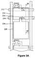
- FIGS. 2A ⁇ 2Care schematic views of a transflective LCD panel according to an embodiment of the invention.
- FIG. 2Ais a top view illustrating an area of approximately one pixel
- FIG. 2B-2Care cross-sectional views respectively taken along sections 2 B- 2 B and 2 C- 2 C in FIG. 2A .
- the transflective LCDincludes gate lines 212 that perpendicularly intersect data lines 214 to define an array of pixel areas.
- the gate lines 212extend into gate pads 216 , respectively in each pixel area.
- a pixel electrode structuregenerally designated as reference numeral 220 .
- the pixel electrode structure 220includes a reflective electrode 222 and a transmissive electrode 224 connected each other.
- the reflective electrode 222constitutes a reflective area
- the transmissive electrode 224constitutes a transmissive area contiguous to the reflective area.
- a switching device 230is respectively coupled with one data line 214 and one gate line 212 to deliver image signals to the pixel electrode structure 220 .
- the switching device 230can be a thin film transistor that has a drain electrode 238 connected to the data line 214 and a source electrode 239 connected to the reflective electrode 222 .
- image datacan be supplied via the data line 214 to the pixel electrode structure 220 for displaying images.
- FIG. 2Bis a cross-sectional view taken across section 2 B- 2 B of FIG. 2A .
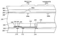
- the transflective LCDincludes a rear substrate 200 and a front substrate 260 assembled parallel to each other to form a cell gap filled with a liquid crystal 250 .
- the rear, front substrates 200 , 260can be made of a transparent material such as glass, quartz or the like.
- the gate line 212 , the gate pad 216 , and a first common voltage electrode 218are formed on a surface of the substrate 200 .
- the gate line 212 , gate pad 216 and first common voltage electrode 218can be formed via patterning a first conductive metal layer made of aluminum (Al), Al alloy, chromium (Cr), molybdenum (Mo), niobium (Nb) or the like.
- a gate-insulating layer 232is formed over the rear substrate 200 to cover the gate pad 216 , the gate line 212 and the first common voltage electrode 218 .
- the gate-insulating layer 232can be silicon oxide or silicon nitride formed by chemical vapor deposition.
- a channel layer 234is formed on the gate-insulating layer 232 across the area of the gate pad 216 .
- the channel layer 234can be doped amorphous silicon formed by plasma-enhanced chemical vapor deposition.
- a cap layer 236is formed on the channel layer 234 at an area above the gate pad 216 .
- the cap layer 236can be made of silicon nitride. Drain and source electrode 238 , 239 are formed on the channel layer 234 , respectively at two sides of the cap layer 236 .
- the cap layer 236can be used as etching stop while patterning a second conductive metal layer to define the drain and source electrodes 238 , 239 .
- the gate pad 216 , gate-insulating layer 232 , drain electrode 238 and source electrode 239constitute a thin film transistor 230 operable as switching device to deliver image signals to the pixel electrode structure 220 .
- the reflective electrode 222is formed on the surface of the gate-insulating layer 232 .
- the reflective electrode 222connects to the source electrode 239 , and extends to an area overlapping the first common voltage electrode 218 .
- the reflective electrode 222 , the source electrode 239 and the drain electrode 238can be formed via patterning a same conductive metal layer having a suitable reflectance.
- a dielectric layer 240is formed over the substrate 200 to cover the thin film transistor 230 and the reflective electrode 222 .
- the characteristics of the dielectric layer 240are selected to regulate the generation of the electric field in the liquid crystal layer 250 .
- the dielectric layer 240is an organic dielectric layer of a low dielectric constant of 3.5, with a thickness of about 1.7 ⁇ m to 2 ⁇ m. Notwithstanding, the dielectric constant of the dielectric layer 240 can be selected lower than 3.5.
- a transmissive electrode 224is formed on a surface of the dielectric layer 240 .
- the transmissive electrode 224can be made of a transparent conductive material such as indium tin oxide, indium zinc oxide or the like.
- the transmissive electrode 224connects to the reflective electrode 222 via a contact hole 226 formed through the dielectric layer 240 .
- a color filter 262 , an insulating layer 264 , and a second common voltage electrode 266are sequentially stacked on an inner surface of the front substrate 260 .
- the color filter 262includes a section 262 a relatively thinner at an area facing the reflective electrode 222 .
- the color filter 262can be formed via a processing method including depositing a color filter material, performing a half-tone exposure to particularly define the section 262 a , and etching the color filter material.
- Protrusions 268 a , 268 bare formed on the second common voltage electrode 266 , respectively in the reflective area and the transmissive area.
- the protrusions 268 a , 268 bcreate boundary conditions resulting in a plurality of domains where the liquid crystal molecules respectively tilt in different directions for displaying images to provide a wider viewing angle.
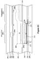
- FIG. 2CReference is made to FIG. 2C to describe the operation of the transflective LCD according to an embodiment of the invention. It is understood that the specific operating voltages disclosed herein are provided as examples and many adequate voltages can be practically implemented to drive the operation of the LCD.
- a voltage potential of 0Vis respectively applied to the first, second common voltage electrodes 218 , 266 , while a voltage potential of 4V is applied via the data line to the reflective and transmissive electrodes 222 , 224 .
- the resulting voltage difference between the pixel electrode structure and the first, second common electrodes 218 , 266create equipotential lines 280 through the liquid crystal layer 250 .
- the levels of the equipotential linesare differently distributed in the reflective and transmissive pixel areas.
- a part 280 a of the equipotential linesis contained within the dielectric layer 240 .
- the controlled equipotential line distributionresults in an electric field, within the liquid crystal layer, which has different strengths in the reflective and transmissive areas, respectively.
- the produced electric fieldis lower in the reflective area than in the transmissive area.
- the effective birefringence ⁇ n of the liquid crystalcan be accordingly modified in the reflective area and the transmissive area.
- the product d ⁇ n characterizing the cell retardationthereby can be controlled and adjusted to obtain an optical performance optimal in both reflective and transmissive areas.
- the liquid crystal displayis conventionally driven according to an inversion mode, i.e. each pixel at two successive display frames is supplied with an image signal of inverted voltage bias.
- an inversion modei.e. each pixel at two successive display frames is supplied with an image signal of inverted voltage bias.
- the reflective electrode 222covers an area W r overlapping with the gate line 212 and the first common voltage electrode 218 .
- the width W g of the gate line 212is entirely covered by the reflective electrode 222 while the width W c of the first common voltage electrode 218 has a portion 218 a uncovered by the reflective electrode 222 .
- This structurecan reduce light leakage due to the electric field contribution from the gate line 212 and provides stable domain boundaries in the liquid crystal layer in inversion mode operation.
- a protrusion 268 bis formed on the second common voltage electrode 266 of the front substrate 260 in the transmissive area, while no protrusion is necessary in the reflective area.
- the reflective electrode 222overlaps with the gate line 212 and the first common voltage electrode 218 . In the overlapping areas, the reflective electrode 222 entirely covers the width W g of the gate line 312 and the width W c of the first common voltage electrode 318 .
- the gate line 212is placed outside the area covered by the pixel electrode structure 220 , and the switching device 230 is formed in an area overlapping the gate line 212 .
- the first common voltage electrode 418includes portions 418 a , 418 b , 418 c uncovered by the reflective, transmissive electrode 222 , 224 .
- the portion 418 ais located in an area 490 a between one gate line 212 and one reflective or transmissive electrode 222 , 224 of an adjacent pixel electrode structure 220 .
- the portion 418 bis located in an area 490 b between one data line 214 and one reflective electrode 222 .
- the portion 418 cis located in an area 490 c between one data line 214 and one transmissive electrode 224 .
- the pixel electrode structurecan include a number of reflective, transmissive electrodes.
- the variation of FIG. 5illustrates a pixel electrode structure 520 that may include two transmissive electrodes 524 alternated with one reflective electrode 522 . More than one reflective, transmissive area can be therefore placed in one pixel.
Landscapes
- Physics & Mathematics (AREA)
- Nonlinear Science (AREA)
- Liquid Crystal (AREA)
- Mathematical Physics (AREA)
- Chemical & Material Sciences (AREA)
- Crystallography & Structural Chemistry (AREA)
- General Physics & Mathematics (AREA)
- Optics & Photonics (AREA)
Abstract
Description
Claims (20)
Priority Applications (5)
| Application Number | Priority Date | Filing Date | Title |
|---|---|---|---|
| US10/857,292US7379135B2 (en) | 2004-05-28 | 2004-05-28 | Transflective liquid crystal display |
| TW093134420ATWI253108B (en) | 2004-05-28 | 2004-11-11 | Transflective liquid crystal display |
| CNB2004101003408ACN100373247C (en) | 2004-05-28 | 2004-12-06 | Transflective liquid crystal display device and pixel electrode structure thereof |
| JP2005148883AJP4346092B2 (en) | 2004-05-28 | 2005-05-23 | Transflective liquid crystal display and pixel electrode structure applied thereto |
| US12/105,097US7508471B2 (en) | 2004-05-28 | 2008-04-17 | Transflective liquid crystal display |
Applications Claiming Priority (1)
| Application Number | Priority Date | Filing Date | Title |
|---|---|---|---|
| US10/857,292US7379135B2 (en) | 2004-05-28 | 2004-05-28 | Transflective liquid crystal display |
Related Child Applications (1)
| Application Number | Title | Priority Date | Filing Date |
|---|---|---|---|
| US12/105,097ContinuationUS7508471B2 (en) | 2004-05-28 | 2008-04-17 | Transflective liquid crystal display |
Publications (2)
| Publication Number | Publication Date |
|---|---|
| US20050264729A1 US20050264729A1 (en) | 2005-12-01 |
| US7379135B2true US7379135B2 (en) | 2008-05-27 |
Family
ID=34795890
Family Applications (2)
| Application Number | Title | Priority Date | Filing Date |
|---|---|---|---|
| US10/857,292Expired - LifetimeUS7379135B2 (en) | 2004-05-28 | 2004-05-28 | Transflective liquid crystal display |
| US12/105,097Expired - LifetimeUS7508471B2 (en) | 2004-05-28 | 2008-04-17 | Transflective liquid crystal display |
Family Applications After (1)
| Application Number | Title | Priority Date | Filing Date |
|---|---|---|---|
| US12/105,097Expired - LifetimeUS7508471B2 (en) | 2004-05-28 | 2008-04-17 | Transflective liquid crystal display |
Country Status (4)
| Country | Link |
|---|---|
| US (2) | US7379135B2 (en) |
| JP (1) | JP4346092B2 (en) |
| CN (1) | CN100373247C (en) |
| TW (1) | TWI253108B (en) |
Cited By (8)
| Publication number | Priority date | Publication date | Assignee | Title |
|---|---|---|---|---|
| US20070013838A1 (en)* | 2005-07-15 | 2007-01-18 | Au Optronics Corp. | Electrode structure and transflective liquid crystal display device using the same |
| US20070153174A1 (en)* | 2005-12-29 | 2007-07-05 | Lg.Philips Lcd Co., Ltd. | Transflective type liquid crystal display device and a method for fabricating the same |
| US20070165167A1 (en)* | 2006-01-18 | 2007-07-19 | Au Optronics Corp. | Liquid crystal display panel and liquid crystal display device incorporating the same |
| US20080055530A1 (en)* | 2006-08-31 | 2008-03-06 | Au Optronics Corp. | Transflective lcd panel, transmissive lcd panel, and reflective lcd panel |
| US20080273130A1 (en)* | 2007-05-01 | 2008-11-06 | Au Optronics Corp. | Display device |
| US20090219476A1 (en)* | 2005-09-30 | 2009-09-03 | Yasutoshi Tasaka | Liquid Crystal Display and Method for Manufacturing Same |
| US20100237348A1 (en)* | 2009-03-19 | 2010-09-23 | Au Optronics Corporation | Thin Film Transistor Array Substrate |
| US20110090428A1 (en)* | 2008-06-17 | 2011-04-21 | Noritaka Ajari | Liquid crystal display device |
Families Citing this family (18)
| Publication number | Priority date | Publication date | Assignee | Title |
|---|---|---|---|---|
| JP3861895B2 (en)* | 2004-09-08 | 2006-12-27 | 三菱電機株式会社 | Transflective liquid crystal display device and manufacturing method thereof |
| JP4606822B2 (en)* | 2004-09-10 | 2011-01-05 | シャープ株式会社 | Manufacturing method of transflective liquid crystal display device |
| US7379138B2 (en)* | 2005-06-09 | 2008-05-27 | Au Optronics Corporation | Transflective liquid crystal display having first and second voltage potentials selected to achieve predetermined polarization states for light encountering respectively the transmissive and reflective areas |
| US7705937B2 (en)* | 2005-06-30 | 2010-04-27 | Nec Lcd Technologies, Ltd. | Transflective liquid crystal display device |
| KR101165751B1 (en) | 2005-07-14 | 2012-07-18 | 삼성전자주식회사 | Liquid crystal display device and method of making the same |
| CN100373243C (en)* | 2005-07-22 | 2008-03-05 | 友达光电股份有限公司 | Electrode and semi-penetrating and semi-reflecting liquid crystal display assembly applying same |
| US7821613B2 (en) | 2005-12-28 | 2010-10-26 | Semiconductor Energy Laboratory Co., Ltd. | Display device and manufacturing method thereof |
| KR101174164B1 (en)* | 2005-12-29 | 2012-08-14 | 엘지디스플레이 주식회사 | Transflective Liquid Crystal Display device |
| CN100388070C (en)* | 2006-01-27 | 2008-05-14 | 友达光电股份有限公司 | Liquid crystal display panel and liquid crystal display device |
| JP2007256843A (en)* | 2006-03-24 | 2007-10-04 | Toshiba Matsushita Display Technology Co Ltd | Liquid crystal display device |
| KR20070109521A (en) | 2006-05-11 | 2007-11-15 | 삼성전자주식회사 | A thin film transistor substrate, a liquid crystal display panel including the same, and a manufacturing method of the liquid crystal display panel |
| US7713596B2 (en) | 2006-06-07 | 2010-05-11 | Chunghwa Picture Tubes, Ltd. | Light shading structure, and color filter substrate, active device array substrate, liquid crystal display panel thereof |
| JP2008009199A (en)* | 2006-06-30 | 2008-01-17 | Sony Corp | Liquid crystal display device |
| CN100495157C (en)* | 2006-07-07 | 2009-06-03 | 中华映管股份有限公司 | Shading structure, color filter substrate, active element array substrate and liquid crystal panel |
| TWI326129B (en)* | 2007-03-21 | 2010-06-11 | Au Optronics Corp | Pixel structure and manufacturing method thereof |
| TWI369554B (en)* | 2007-12-27 | 2012-08-01 | Au Optronics Corp | Pixel structure and manufacturing method thereof |
| US11428982B2 (en)* | 2018-07-04 | 2022-08-30 | Sony Corporation | Electrode structure, method for manufacturing electrode structure, liquid crystal display element, method for driving liquid crystal display element, and electronic equipment |
| WO2021182037A1 (en)* | 2020-03-09 | 2021-09-16 | 株式会社村田製作所 | Antenna module and communication device equipped with same |
Citations (24)
| Publication number | Priority date | Publication date | Assignee | Title |
|---|---|---|---|---|
| US4714983A (en) | 1985-06-10 | 1987-12-22 | Motorola, Inc. | Uniform emission backlight |
| US5641974A (en)* | 1995-06-06 | 1997-06-24 | Ois Optical Imaging Systems, Inc. | LCD with bus lines overlapped by pixel electrodes and photo-imageable insulating layer therebetween |
| US5841494A (en) | 1996-06-26 | 1998-11-24 | Hall; Dennis R. | Transflective LCD utilizing chiral liquid crystal filter/mirrors |
| US6008871A (en) | 1997-01-20 | 1999-12-28 | Seiko Epson Corporation | Transflective liquid crystal display device having a reflective polarizer |
| US6124905A (en) | 1997-09-18 | 2000-09-26 | Seiko Epson Corporation | Display device employing a reflective polarizer and a reflective diffuser between a light source and the display device |
| US6199989B1 (en) | 1998-10-29 | 2001-03-13 | Sumitomo Chemical Company, Limited | Optical plate having reflecting function and transmitting function |
| US6466280B1 (en) | 1999-08-06 | 2002-10-15 | Lg. Philips Lcd Co., Ltd. | Transflective liquid crystal display device and method of manufacturing the same |
| US6508560B2 (en) | 1999-10-22 | 2003-01-21 | 3M Innovative Properties Company | Display apparatus with corrosion-resistant light directing film |
| US20030025859A1 (en) | 2001-08-01 | 2003-02-06 | Kook-Chul Moon | Transreflective type liquid crystal display and method of manufacaturing the same |
| US6567060B1 (en) | 1997-10-16 | 2003-05-20 | Citizen Watch Co., Ltd. | Liquid display |
| US6567141B1 (en) | 1999-02-23 | 2003-05-20 | Citizen Watch Co., Ltd. | Liquid crystal display |
| US6574044B1 (en) | 1999-10-25 | 2003-06-03 | 3M Innovative Properties Company | Polarizer constructions and display devices exhibiting unique color effects |
| US6577361B1 (en) | 1998-12-09 | 2003-06-10 | Citizen Watch Co., Ltd. | Liquid crystal display |
| US6580480B2 (en) | 2000-07-04 | 2003-06-17 | Lg. Phillips Lcd Co., Ltd. | Transflective liquid crystal display device and manufacturing method thereof |
| US6606139B2 (en) | 2001-04-19 | 2003-08-12 | Alps Electric Co., Ltd. | Liquid crystal display device with improved viewing angle property and portable electronic apparatus using the same |
| US6608660B1 (en) | 1999-07-16 | 2003-08-19 | Seiko Epson Corporation | Liquid crystal display device including shading film with opening and reflector with opening in the opening in the shading film |
| US6611305B2 (en) | 2000-03-14 | 2003-08-26 | Seiko Epson Corporation | Liquid crystal display device and electronic apparatus |
| US6628369B2 (en) | 2000-03-10 | 2003-09-30 | Nippon Oil Corporation | Circular polarizer and liquid crystal display |
| JP2003279945A (en) | 2002-03-25 | 2003-10-02 | Matsushita Electric Ind Co Ltd | Liquid crystal display |
| US20040085498A1 (en)* | 2002-11-05 | 2004-05-06 | Wei-Chih Chang | Transflective liquid crystal display |
| US20040165129A1 (en)* | 2002-12-20 | 2004-08-26 | Seiko Epson Corporation | Liquid crystal display device and electronic equipment |
| US20040218123A1 (en)* | 2003-04-30 | 2004-11-04 | Samsung Electronics Co., Ltd | Upper substrate, liquid crystal display apparatus having the same and method of manufacturing the same |
| US6922219B2 (en)* | 2002-08-14 | 2005-07-26 | Lg. Philips Lcd Co., Ltd. | Transflective liquid crystal display |
| US6956632B2 (en)* | 2001-09-25 | 2005-10-18 | Seiko Epson Corporation | Transflective liquid crystal device with particular stack of reflective, transmissive, and thickness adjusting layers and electronic device using the same |
Family Cites Families (1)
| Publication number | Priority date | Publication date | Assignee | Title |
|---|---|---|---|---|
| CA2435684A1 (en)* | 2002-07-19 | 2004-01-19 | Basic American Medical Products, Inc. | Height and angle adjustable bed |
- 2004
- 2004-05-28USUS10/857,292patent/US7379135B2/ennot_activeExpired - Lifetime
- 2004-11-11TWTW093134420Apatent/TWI253108B/ennot_activeIP Right Cessation
- 2004-12-06CNCNB2004101003408Apatent/CN100373247C/ennot_activeExpired - Lifetime
- 2005
- 2005-05-23JPJP2005148883Apatent/JP4346092B2/ennot_activeExpired - Lifetime
- 2008
- 2008-04-17USUS12/105,097patent/US7508471B2/ennot_activeExpired - Lifetime
Patent Citations (25)
| Publication number | Priority date | Publication date | Assignee | Title |
|---|---|---|---|---|
| US4714983A (en) | 1985-06-10 | 1987-12-22 | Motorola, Inc. | Uniform emission backlight |
| US5641974A (en)* | 1995-06-06 | 1997-06-24 | Ois Optical Imaging Systems, Inc. | LCD with bus lines overlapped by pixel electrodes and photo-imageable insulating layer therebetween |
| US5841494A (en) | 1996-06-26 | 1998-11-24 | Hall; Dennis R. | Transflective LCD utilizing chiral liquid crystal filter/mirrors |
| US6008871A (en) | 1997-01-20 | 1999-12-28 | Seiko Epson Corporation | Transflective liquid crystal display device having a reflective polarizer |
| US6124905A (en) | 1997-09-18 | 2000-09-26 | Seiko Epson Corporation | Display device employing a reflective polarizer and a reflective diffuser between a light source and the display device |
| US6567060B1 (en) | 1997-10-16 | 2003-05-20 | Citizen Watch Co., Ltd. | Liquid display |
| US6199989B1 (en) | 1998-10-29 | 2001-03-13 | Sumitomo Chemical Company, Limited | Optical plate having reflecting function and transmitting function |
| US6577361B1 (en) | 1998-12-09 | 2003-06-10 | Citizen Watch Co., Ltd. | Liquid crystal display |
| US6567141B1 (en) | 1999-02-23 | 2003-05-20 | Citizen Watch Co., Ltd. | Liquid crystal display |
| US6608660B1 (en) | 1999-07-16 | 2003-08-19 | Seiko Epson Corporation | Liquid crystal display device including shading film with opening and reflector with opening in the opening in the shading film |
| US6466280B1 (en) | 1999-08-06 | 2002-10-15 | Lg. Philips Lcd Co., Ltd. | Transflective liquid crystal display device and method of manufacturing the same |
| US6508560B2 (en) | 1999-10-22 | 2003-01-21 | 3M Innovative Properties Company | Display apparatus with corrosion-resistant light directing film |
| US6574044B1 (en) | 1999-10-25 | 2003-06-03 | 3M Innovative Properties Company | Polarizer constructions and display devices exhibiting unique color effects |
| US6628369B2 (en) | 2000-03-10 | 2003-09-30 | Nippon Oil Corporation | Circular polarizer and liquid crystal display |
| US6611305B2 (en) | 2000-03-14 | 2003-08-26 | Seiko Epson Corporation | Liquid crystal display device and electronic apparatus |
| US6580480B2 (en) | 2000-07-04 | 2003-06-17 | Lg. Phillips Lcd Co., Ltd. | Transflective liquid crystal display device and manufacturing method thereof |
| US6606139B2 (en) | 2001-04-19 | 2003-08-12 | Alps Electric Co., Ltd. | Liquid crystal display device with improved viewing angle property and portable electronic apparatus using the same |
| US20030025859A1 (en) | 2001-08-01 | 2003-02-06 | Kook-Chul Moon | Transreflective type liquid crystal display and method of manufacaturing the same |
| US6879361B2 (en)* | 2001-08-01 | 2005-04-12 | Samsung Electronics Co., Ltd. | Transreflective liquid crystal display and method of manufacturing the same |
| US6956632B2 (en)* | 2001-09-25 | 2005-10-18 | Seiko Epson Corporation | Transflective liquid crystal device with particular stack of reflective, transmissive, and thickness adjusting layers and electronic device using the same |
| JP2003279945A (en) | 2002-03-25 | 2003-10-02 | Matsushita Electric Ind Co Ltd | Liquid crystal display |
| US6922219B2 (en)* | 2002-08-14 | 2005-07-26 | Lg. Philips Lcd Co., Ltd. | Transflective liquid crystal display |
| US20040085498A1 (en)* | 2002-11-05 | 2004-05-06 | Wei-Chih Chang | Transflective liquid crystal display |
| US20040165129A1 (en)* | 2002-12-20 | 2004-08-26 | Seiko Epson Corporation | Liquid crystal display device and electronic equipment |
| US20040218123A1 (en)* | 2003-04-30 | 2004-11-04 | Samsung Electronics Co., Ltd | Upper substrate, liquid crystal display apparatus having the same and method of manufacturing the same |
Cited By (20)
| Publication number | Priority date | Publication date | Assignee | Title |
|---|---|---|---|---|
| US20070013838A1 (en)* | 2005-07-15 | 2007-01-18 | Au Optronics Corp. | Electrode structure and transflective liquid crystal display device using the same |
| US7656481B2 (en)* | 2005-07-15 | 2010-02-02 | Au Optronics Corp. | Electrode structure and transflective liquid crystal display device using the same |
| US20090219476A1 (en)* | 2005-09-30 | 2009-09-03 | Yasutoshi Tasaka | Liquid Crystal Display and Method for Manufacturing Same |
| US7978295B2 (en)* | 2005-09-30 | 2011-07-12 | Sharp Kabushiki Kaisha | Liquid crystal display and method for manufacturing same |
| US20070153174A1 (en)* | 2005-12-29 | 2007-07-05 | Lg.Philips Lcd Co., Ltd. | Transflective type liquid crystal display device and a method for fabricating the same |
| US7724329B2 (en)* | 2005-12-29 | 2010-05-25 | Lg Display Co., Ltd. | Transflective type liquid crystal display device and a method for fabricating the same |
| US7903213B2 (en) | 2006-01-18 | 2011-03-08 | Au Optronics Corp. | Liquid crystal display panel and liquid crystal display device incorporating the same |
| US7701536B2 (en)* | 2006-01-18 | 2010-04-20 | Au Optronics Corp. | Liquid crystal display panel and liquid crystal display device incorporating the same |
| US20090296009A1 (en)* | 2006-01-18 | 2009-12-03 | Ching-Yu Tsai | Liquid crystal display panel and liquid crystal display device incorporating the same |
| US20070165167A1 (en)* | 2006-01-18 | 2007-07-19 | Au Optronics Corp. | Liquid crystal display panel and liquid crystal display device incorporating the same |
| US7928528B2 (en)* | 2006-08-31 | 2011-04-19 | Au Optronics Corp. | Transflective LCD panel, transmissive LCD panel, and reflective LCD panel |
| US7781857B2 (en)* | 2006-08-31 | 2010-08-24 | Au Optronics Corp. | Transflective LCD panel, transmissive LCD panel, and reflective LCD panel |
| US20100277662A1 (en)* | 2006-08-31 | 2010-11-04 | Au Optronics Corp. | Transflective LCD Panel, Transmissive LCD Panel, and Reflective LCD Panel |
| US20080055530A1 (en)* | 2006-08-31 | 2008-03-06 | Au Optronics Corp. | Transflective lcd panel, transmissive lcd panel, and reflective lcd panel |
| US20090180067A1 (en)* | 2006-08-31 | 2009-07-16 | Au Optronics Corp. | Transflective lcd panel, transmissive lcd panel, and reflective lcd panel |
| US7525169B2 (en)* | 2006-08-31 | 2009-04-28 | Au Optronics Corp. | Transflective LCD panel, transmissive LCD panel, and reflective LCD panel |
| US20080273130A1 (en)* | 2007-05-01 | 2008-11-06 | Au Optronics Corp. | Display device |
| US20110090428A1 (en)* | 2008-06-17 | 2011-04-21 | Noritaka Ajari | Liquid crystal display device |
| US20100237348A1 (en)* | 2009-03-19 | 2010-09-23 | Au Optronics Corporation | Thin Film Transistor Array Substrate |
| US8455877B2 (en) | 2009-03-19 | 2013-06-04 | Au Optronics Corporation | Thin film transistor array substrate |
Also Published As
| Publication number | Publication date |
|---|---|
| TW200539317A (en) | 2005-12-01 |
| JP2005338829A (en) | 2005-12-08 |
| CN100373247C (en) | 2008-03-05 |
| US7508471B2 (en) | 2009-03-24 |
| TWI253108B (en) | 2006-04-11 |
| JP4346092B2 (en) | 2009-10-14 |
| CN1619402A (en) | 2005-05-25 |
| US20050264729A1 (en) | 2005-12-01 |
| US20080192187A1 (en) | 2008-08-14 |
Similar Documents
| Publication | Publication Date | Title |
|---|---|---|
| US7508471B2 (en) | Transflective liquid crystal display | |
| CN103529608B (en) | Array base palte and manufacture method thereof for liquid crystal display | |
| US5852485A (en) | Liquid crystal display device and method for producing the same | |
| US6262784B1 (en) | Active matrix display devices having improved opening and contrast ratios and methods of forming same and a storage electrode line | |
| US8976328B2 (en) | Liquid crystal display device and method for fabricating the same | |
| KR100713188B1 (en) | Active matrix liquid crystal display apparatus | |
| US8040481B2 (en) | In-plane switching mode liquid crystal display device having first and second common electrode connection lines and first and second pixel electrode connection linesbeing formed on the same layer | |
| US8531639B2 (en) | Liquid crystal display device | |
| US7206050B2 (en) | IPS type LCD and method for fabricating the same | |
| CN101387806B (en) | Liquid crystal display panel and manufacturing method thereof | |
| CN101082728B (en) | Transflective liquid crystal display device | |
| US20080001883A1 (en) | Liquid Crystal Display Device and Method for Fabricating the Same | |
| JP5460123B2 (en) | Liquid crystal display | |
| US20080180623A1 (en) | Liquid crystal display device | |
| KR20010106862A (en) | IPS mode Liquid crystal display device and method for fabricating the same | |
| US8922743B2 (en) | Liquid crystal display device and method of fabricating the same | |
| KR100731045B1 (en) | Transverse electric field type liquid crystal display device and manufacturing method thereof | |
| US6853427B2 (en) | Liquid crystal display device and method for manufacturing the same | |
| US7538838B2 (en) | Semi-transmissive liquid crystal display panel | |
| US7932961B2 (en) | Liquid crystal display device having light blocking line disposed on same layer as gate line | |
| US20080273130A1 (en) | Display device | |
| US8120734B2 (en) | Transflective liquid crystal display and fabrication method thereof | |
| JP3199221B2 (en) | Liquid crystal display device and manufacturing method thereof | |
| US6891579B2 (en) | Liquid crystal display panel and method for manufacturing the same | |
| US20080036952A1 (en) | Liquid crystal display device |
Legal Events
| Date | Code | Title | Description |
|---|---|---|---|
| AS | Assignment | Owner name:AU OPTRONICS CORPORATION, TAIWAN Free format text:ASSIGNMENT OF ASSIGNORS INTEREST;ASSIGNORS:LIN, CHING-HUAN;CHANG, CHIN-MING;TSAI, CHING-YU;AND OTHERS;REEL/FRAME:015595/0468 Effective date:20040521 Owner name:FUJITSU DISPLAY TECHNOLOGIES CORPORATION, JAPAN Free format text:ASSIGNMENT OF ASSIGNORS INTEREST;ASSIGNORS:LIN, CHING-HUAN;CHANG, CHIN-MING;TSAI, CHING-YU;AND OTHERS;REEL/FRAME:015595/0468 Effective date:20040521 | |
| AS | Assignment | Owner name:FUJITSU LIMITED, JAPAN Free format text:CHANGE OF NAME;ASSIGNOR:FUJITSU DISPLAY TECHNOLOGIES CORPORATION;REEL/FRAME:017238/0946 Effective date:20060119 | |
| STCF | Information on status: patent grant | Free format text:PATENTED CASE | |
| CC | Certificate of correction | ||
| AS | Assignment | Owner name:AU OPTRONICS CORPORATION, TAIWAN Free format text:ASSIGNMENT OF ASSIGNORS INTEREST;ASSIGNOR:FUJITSU LIMITED;REEL/FRAME:027068/0612 Effective date:20111014 | |
| FPAY | Fee payment | Year of fee payment:4 | |
| FPAY | Fee payment | Year of fee payment:8 | |
| MAFP | Maintenance fee payment | Free format text:PAYMENT OF MAINTENANCE FEE, 12TH YEAR, LARGE ENTITY (ORIGINAL EVENT CODE: M1553); ENTITY STATUS OF PATENT OWNER: LARGE ENTITY Year of fee payment:12 |