US7378737B2 - Structures and methods to enhance copper metallization - Google Patents
Structures and methods to enhance copper metallizationDownload PDFInfo
- Publication number
- US7378737B2 US7378737B2US10/196,081US19608102AUS7378737B2US 7378737 B2US7378737 B2US 7378737B2US 19608102 AUS19608102 AUS 19608102AUS 7378737 B2US7378737 B2US 7378737B2
- Authority
- US
- United States
- Prior art keywords
- insulator
- layer
- protective layer
- copper
- semiconductor structure
- Prior art date
- Legal status (The legal status is an assumption and is not a legal conclusion. Google has not performed a legal analysis and makes no representation as to the accuracy of the status listed.)
- Expired - Fee Related
Links
Images


Classifications
- H—ELECTRICITY
- H01—ELECTRIC ELEMENTS
- H01L—SEMICONDUCTOR DEVICES NOT COVERED BY CLASS H10
- H01L21/00—Processes or apparatus adapted for the manufacture or treatment of semiconductor or solid state devices or of parts thereof
- H01L21/02—Manufacture or treatment of semiconductor devices or of parts thereof
- H01L21/04—Manufacture or treatment of semiconductor devices or of parts thereof the devices having potential barriers, e.g. a PN junction, depletion layer or carrier concentration layer
- H01L21/18—Manufacture or treatment of semiconductor devices or of parts thereof the devices having potential barriers, e.g. a PN junction, depletion layer or carrier concentration layer the devices having semiconductor bodies comprising elements of Group IV of the Periodic Table or AIIIBV compounds with or without impurities, e.g. doping materials
- H01L21/30—Treatment of semiconductor bodies using processes or apparatus not provided for in groups H01L21/20 - H01L21/26
- H01L21/31—Treatment of semiconductor bodies using processes or apparatus not provided for in groups H01L21/20 - H01L21/26 to form insulating layers thereon, e.g. for masking or by using photolithographic techniques; After treatment of these layers; Selection of materials for these layers
- H01L21/3205—Deposition of non-insulating-, e.g. conductive- or resistive-, layers on insulating layers; After-treatment of these layers
- H01L21/32051—Deposition of metallic or metal-silicide layers
- H—ELECTRICITY
- H01—ELECTRIC ELEMENTS
- H01L—SEMICONDUCTOR DEVICES NOT COVERED BY CLASS H10
- H01L21/00—Processes or apparatus adapted for the manufacture or treatment of semiconductor or solid state devices or of parts thereof
- H01L21/70—Manufacture or treatment of devices consisting of a plurality of solid state components formed in or on a common substrate or of parts thereof; Manufacture of integrated circuit devices or of parts thereof
- H01L21/71—Manufacture of specific parts of devices defined in group H01L21/70
- H01L21/768—Applying interconnections to be used for carrying current between separate components within a device comprising conductors and dielectrics
- H01L21/76838—Applying interconnections to be used for carrying current between separate components within a device comprising conductors and dielectrics characterised by the formation and the after-treatment of the conductors
- H01L21/76841—Barrier, adhesion or liner layers
- H—ELECTRICITY
- H01—ELECTRIC ELEMENTS
- H01L—SEMICONDUCTOR DEVICES NOT COVERED BY CLASS H10
- H01L21/00—Processes or apparatus adapted for the manufacture or treatment of semiconductor or solid state devices or of parts thereof
- H01L21/70—Manufacture or treatment of devices consisting of a plurality of solid state components formed in or on a common substrate or of parts thereof; Manufacture of integrated circuit devices or of parts thereof
- H01L21/71—Manufacture of specific parts of devices defined in group H01L21/70
- H01L21/768—Applying interconnections to be used for carrying current between separate components within a device comprising conductors and dielectrics
- H01L21/76801—Applying interconnections to be used for carrying current between separate components within a device comprising conductors and dielectrics characterised by the formation and the after-treatment of the dielectrics, e.g. smoothing
- H01L21/76802—Applying interconnections to be used for carrying current between separate components within a device comprising conductors and dielectrics characterised by the formation and the after-treatment of the dielectrics, e.g. smoothing by forming openings in dielectrics
- H01L21/76814—Applying interconnections to be used for carrying current between separate components within a device comprising conductors and dielectrics characterised by the formation and the after-treatment of the dielectrics, e.g. smoothing by forming openings in dielectrics post-treatment or after-treatment, e.g. cleaning or removal of oxides on underlying conductors
- H—ELECTRICITY
- H01—ELECTRIC ELEMENTS
- H01L—SEMICONDUCTOR DEVICES NOT COVERED BY CLASS H10
- H01L21/00—Processes or apparatus adapted for the manufacture or treatment of semiconductor or solid state devices or of parts thereof
- H01L21/70—Manufacture or treatment of devices consisting of a plurality of solid state components formed in or on a common substrate or of parts thereof; Manufacture of integrated circuit devices or of parts thereof
- H01L21/71—Manufacture of specific parts of devices defined in group H01L21/70
- H01L21/768—Applying interconnections to be used for carrying current between separate components within a device comprising conductors and dielectrics
- H01L21/76801—Applying interconnections to be used for carrying current between separate components within a device comprising conductors and dielectrics characterised by the formation and the after-treatment of the dielectrics, e.g. smoothing
- H01L21/76822—Modification of the material of dielectric layers, e.g. grading, after-treatment to improve the stability of the layers, to increase their density etc.
- H01L21/76823—Modification of the material of dielectric layers, e.g. grading, after-treatment to improve the stability of the layers, to increase their density etc. transforming an insulating layer into a conductive layer
- H—ELECTRICITY
- H01—ELECTRIC ELEMENTS
- H01L—SEMICONDUCTOR DEVICES NOT COVERED BY CLASS H10
- H01L21/00—Processes or apparatus adapted for the manufacture or treatment of semiconductor or solid state devices or of parts thereof
- H01L21/70—Manufacture or treatment of devices consisting of a plurality of solid state components formed in or on a common substrate or of parts thereof; Manufacture of integrated circuit devices or of parts thereof
- H01L21/71—Manufacture of specific parts of devices defined in group H01L21/70
- H01L21/768—Applying interconnections to be used for carrying current between separate components within a device comprising conductors and dielectrics
- H01L21/76801—Applying interconnections to be used for carrying current between separate components within a device comprising conductors and dielectrics characterised by the formation and the after-treatment of the dielectrics, e.g. smoothing
- H01L21/76822—Modification of the material of dielectric layers, e.g. grading, after-treatment to improve the stability of the layers, to increase their density etc.
- H01L21/76825—Modification of the material of dielectric layers, e.g. grading, after-treatment to improve the stability of the layers, to increase their density etc. by exposing the layer to particle radiation, e.g. ion implantation, irradiation with UV light or electrons etc.
- H—ELECTRICITY
- H01—ELECTRIC ELEMENTS
- H01L—SEMICONDUCTOR DEVICES NOT COVERED BY CLASS H10
- H01L21/00—Processes or apparatus adapted for the manufacture or treatment of semiconductor or solid state devices or of parts thereof
- H01L21/70—Manufacture or treatment of devices consisting of a plurality of solid state components formed in or on a common substrate or of parts thereof; Manufacture of integrated circuit devices or of parts thereof
- H01L21/71—Manufacture of specific parts of devices defined in group H01L21/70
- H01L21/768—Applying interconnections to be used for carrying current between separate components within a device comprising conductors and dielectrics
- H01L21/76801—Applying interconnections to be used for carrying current between separate components within a device comprising conductors and dielectrics characterised by the formation and the after-treatment of the dielectrics, e.g. smoothing
- H01L21/76822—Modification of the material of dielectric layers, e.g. grading, after-treatment to improve the stability of the layers, to increase their density etc.
- H01L21/76828—Modification of the material of dielectric layers, e.g. grading, after-treatment to improve the stability of the layers, to increase their density etc. thermal treatment
- H—ELECTRICITY
- H01—ELECTRIC ELEMENTS
- H01L—SEMICONDUCTOR DEVICES NOT COVERED BY CLASS H10
- H01L21/00—Processes or apparatus adapted for the manufacture or treatment of semiconductor or solid state devices or of parts thereof
- H01L21/70—Manufacture or treatment of devices consisting of a plurality of solid state components formed in or on a common substrate or of parts thereof; Manufacture of integrated circuit devices or of parts thereof
- H01L21/71—Manufacture of specific parts of devices defined in group H01L21/70
- H01L21/768—Applying interconnections to be used for carrying current between separate components within a device comprising conductors and dielectrics
- H01L21/76801—Applying interconnections to be used for carrying current between separate components within a device comprising conductors and dielectrics characterised by the formation and the after-treatment of the dielectrics, e.g. smoothing
- H01L21/76829—Applying interconnections to be used for carrying current between separate components within a device comprising conductors and dielectrics characterised by the formation and the after-treatment of the dielectrics, e.g. smoothing characterised by the formation of thin functional dielectric layers, e.g. dielectric etch-stop, barrier, capping or liner layers
- H01L21/76831—Applying interconnections to be used for carrying current between separate components within a device comprising conductors and dielectrics characterised by the formation and the after-treatment of the dielectrics, e.g. smoothing characterised by the formation of thin functional dielectric layers, e.g. dielectric etch-stop, barrier, capping or liner layers in via holes or trenches, e.g. non-conductive sidewall liners
- H—ELECTRICITY
- H01—ELECTRIC ELEMENTS
- H01L—SEMICONDUCTOR DEVICES NOT COVERED BY CLASS H10
- H01L21/00—Processes or apparatus adapted for the manufacture or treatment of semiconductor or solid state devices or of parts thereof
- H01L21/70—Manufacture or treatment of devices consisting of a plurality of solid state components formed in or on a common substrate or of parts thereof; Manufacture of integrated circuit devices or of parts thereof
- H01L21/71—Manufacture of specific parts of devices defined in group H01L21/70
- H01L21/768—Applying interconnections to be used for carrying current between separate components within a device comprising conductors and dielectrics
- H01L21/76838—Applying interconnections to be used for carrying current between separate components within a device comprising conductors and dielectrics characterised by the formation and the after-treatment of the conductors
- H01L21/76841—Barrier, adhesion or liner layers
- H01L21/76843—Barrier, adhesion or liner layers formed in openings in a dielectric
- H—ELECTRICITY
- H01—ELECTRIC ELEMENTS
- H01L—SEMICONDUCTOR DEVICES NOT COVERED BY CLASS H10
- H01L21/00—Processes or apparatus adapted for the manufacture or treatment of semiconductor or solid state devices or of parts thereof
- H01L21/70—Manufacture or treatment of devices consisting of a plurality of solid state components formed in or on a common substrate or of parts thereof; Manufacture of integrated circuit devices or of parts thereof
- H01L21/71—Manufacture of specific parts of devices defined in group H01L21/70
- H01L21/768—Applying interconnections to be used for carrying current between separate components within a device comprising conductors and dielectrics
- H01L21/76838—Applying interconnections to be used for carrying current between separate components within a device comprising conductors and dielectrics characterised by the formation and the after-treatment of the conductors
- H01L21/76841—Barrier, adhesion or liner layers
- H01L21/76853—Barrier, adhesion or liner layers characterized by particular after-treatment steps
- H01L21/76855—After-treatment introducing at least one additional element into the layer
- H01L21/76859—After-treatment introducing at least one additional element into the layer by ion implantation
- H—ELECTRICITY
- H01—ELECTRIC ELEMENTS
- H01L—SEMICONDUCTOR DEVICES NOT COVERED BY CLASS H10
- H01L21/00—Processes or apparatus adapted for the manufacture or treatment of semiconductor or solid state devices or of parts thereof
- H01L21/70—Manufacture or treatment of devices consisting of a plurality of solid state components formed in or on a common substrate or of parts thereof; Manufacture of integrated circuit devices or of parts thereof
- H01L21/71—Manufacture of specific parts of devices defined in group H01L21/70
- H01L21/768—Applying interconnections to be used for carrying current between separate components within a device comprising conductors and dielectrics
- H01L21/76838—Applying interconnections to be used for carrying current between separate components within a device comprising conductors and dielectrics characterised by the formation and the after-treatment of the conductors
- H01L21/76841—Barrier, adhesion or liner layers
- H01L21/76867—Barrier, adhesion or liner layers characterized by methods of formation other than PVD, CVD or deposition from a liquids
- H—ELECTRICITY
- H01—ELECTRIC ELEMENTS
- H01L—SEMICONDUCTOR DEVICES NOT COVERED BY CLASS H10
- H01L21/00—Processes or apparatus adapted for the manufacture or treatment of semiconductor or solid state devices or of parts thereof
- H01L21/70—Manufacture or treatment of devices consisting of a plurality of solid state components formed in or on a common substrate or of parts thereof; Manufacture of integrated circuit devices or of parts thereof
- H01L21/71—Manufacture of specific parts of devices defined in group H01L21/70
- H01L21/768—Applying interconnections to be used for carrying current between separate components within a device comprising conductors and dielectrics
- H01L21/76838—Applying interconnections to be used for carrying current between separate components within a device comprising conductors and dielectrics characterised by the formation and the after-treatment of the conductors
- H01L21/76841—Barrier, adhesion or liner layers
- H01L21/76871—Layers specifically deposited to enhance or enable the nucleation of further layers, i.e. seed layers
- H01L21/76873—Layers specifically deposited to enhance or enable the nucleation of further layers, i.e. seed layers for electroplating
- H—ELECTRICITY
- H01—ELECTRIC ELEMENTS
- H01L—SEMICONDUCTOR DEVICES NOT COVERED BY CLASS H10
- H01L21/00—Processes or apparatus adapted for the manufacture or treatment of semiconductor or solid state devices or of parts thereof
- H01L21/70—Manufacture or treatment of devices consisting of a plurality of solid state components formed in or on a common substrate or of parts thereof; Manufacture of integrated circuit devices or of parts thereof
- H01L21/71—Manufacture of specific parts of devices defined in group H01L21/70
- H01L21/768—Applying interconnections to be used for carrying current between separate components within a device comprising conductors and dielectrics
- H01L21/76838—Applying interconnections to be used for carrying current between separate components within a device comprising conductors and dielectrics characterised by the formation and the after-treatment of the conductors
- H01L21/76841—Barrier, adhesion or liner layers
- H01L21/76871—Layers specifically deposited to enhance or enable the nucleation of further layers, i.e. seed layers
- H01L21/76874—Layers specifically deposited to enhance or enable the nucleation of further layers, i.e. seed layers for electroless plating
- H—ELECTRICITY
- H01—ELECTRIC ELEMENTS
- H01L—SEMICONDUCTOR DEVICES NOT COVERED BY CLASS H10
- H01L21/00—Processes or apparatus adapted for the manufacture or treatment of semiconductor or solid state devices or of parts thereof
- H01L21/70—Manufacture or treatment of devices consisting of a plurality of solid state components formed in or on a common substrate or of parts thereof; Manufacture of integrated circuit devices or of parts thereof
- H01L21/71—Manufacture of specific parts of devices defined in group H01L21/70
- H01L21/768—Applying interconnections to be used for carrying current between separate components within a device comprising conductors and dielectrics
- H01L21/76838—Applying interconnections to be used for carrying current between separate components within a device comprising conductors and dielectrics characterised by the formation and the after-treatment of the conductors
- H01L21/76877—Filling of holes, grooves or trenches, e.g. vias, with conductive material
- H01L21/76879—Filling of holes, grooves or trenches, e.g. vias, with conductive material by selective deposition of conductive material in the vias, e.g. selective C.V.D. on semiconductor material, plating
- H—ELECTRICITY
- H01—ELECTRIC ELEMENTS
- H01L—SEMICONDUCTOR DEVICES NOT COVERED BY CLASS H10
- H01L21/00—Processes or apparatus adapted for the manufacture or treatment of semiconductor or solid state devices or of parts thereof
- H01L21/70—Manufacture or treatment of devices consisting of a plurality of solid state components formed in or on a common substrate or of parts thereof; Manufacture of integrated circuit devices or of parts thereof
- H01L21/71—Manufacture of specific parts of devices defined in group H01L21/70
- H01L21/768—Applying interconnections to be used for carrying current between separate components within a device comprising conductors and dielectrics
- H01L21/76838—Applying interconnections to be used for carrying current between separate components within a device comprising conductors and dielectrics characterised by the formation and the after-treatment of the conductors
- H01L21/76877—Filling of holes, grooves or trenches, e.g. vias, with conductive material
- H01L21/7688—Filling of holes, grooves or trenches, e.g. vias, with conductive material by deposition over sacrificial masking layer, e.g. lift-off
- H—ELECTRICITY
- H01—ELECTRIC ELEMENTS
- H01L—SEMICONDUCTOR DEVICES NOT COVERED BY CLASS H10
- H01L23/00—Details of semiconductor or other solid state devices
- H01L23/52—Arrangements for conducting electric current within the device in operation from one component to another, i.e. interconnections, e.g. wires, lead frames
- H01L23/522—Arrangements for conducting electric current within the device in operation from one component to another, i.e. interconnections, e.g. wires, lead frames including external interconnections consisting of a multilayer structure of conductive and insulating layers inseparably formed on the semiconductor body
- H01L23/532—Arrangements for conducting electric current within the device in operation from one component to another, i.e. interconnections, e.g. wires, lead frames including external interconnections consisting of a multilayer structure of conductive and insulating layers inseparably formed on the semiconductor body characterised by the materials
- H01L23/53204—Conductive materials
- H01L23/53209—Conductive materials based on metals, e.g. alloys, metal silicides
- H01L23/53228—Conductive materials based on metals, e.g. alloys, metal silicides the principal metal being copper
- H01L23/53238—Additional layers associated with copper layers, e.g. adhesion, barrier, cladding layers
- H—ELECTRICITY
- H01—ELECTRIC ELEMENTS
- H01L—SEMICONDUCTOR DEVICES NOT COVERED BY CLASS H10
- H01L23/00—Details of semiconductor or other solid state devices
- H01L23/52—Arrangements for conducting electric current within the device in operation from one component to another, i.e. interconnections, e.g. wires, lead frames
- H01L23/522—Arrangements for conducting electric current within the device in operation from one component to another, i.e. interconnections, e.g. wires, lead frames including external interconnections consisting of a multilayer structure of conductive and insulating layers inseparably formed on the semiconductor body
- H01L23/532—Arrangements for conducting electric current within the device in operation from one component to another, i.e. interconnections, e.g. wires, lead frames including external interconnections consisting of a multilayer structure of conductive and insulating layers inseparably formed on the semiconductor body characterised by the materials
- H01L23/5329—Insulating materials
- H01L23/53295—Stacked insulating layers
- H—ELECTRICITY
- H01—ELECTRIC ELEMENTS
- H01L—SEMICONDUCTOR DEVICES NOT COVERED BY CLASS H10
- H01L23/00—Details of semiconductor or other solid state devices
- H01L23/52—Arrangements for conducting electric current within the device in operation from one component to another, i.e. interconnections, e.g. wires, lead frames
- H01L23/522—Arrangements for conducting electric current within the device in operation from one component to another, i.e. interconnections, e.g. wires, lead frames including external interconnections consisting of a multilayer structure of conductive and insulating layers inseparably formed on the semiconductor body
- H01L23/532—Arrangements for conducting electric current within the device in operation from one component to another, i.e. interconnections, e.g. wires, lead frames including external interconnections consisting of a multilayer structure of conductive and insulating layers inseparably formed on the semiconductor body characterised by the materials
- H01L23/53204—Conductive materials
- H01L23/53209—Conductive materials based on metals, e.g. alloys, metal silicides
- H01L23/53228—Conductive materials based on metals, e.g. alloys, metal silicides the principal metal being copper
- H—ELECTRICITY
- H01—ELECTRIC ELEMENTS
- H01L—SEMICONDUCTOR DEVICES NOT COVERED BY CLASS H10
- H01L2924/00—Indexing scheme for arrangements or methods for connecting or disconnecting semiconductor or solid-state bodies as covered by H01L24/00
- H01L2924/0001—Technical content checked by a classifier
- H01L2924/0002—Not covered by any one of groups H01L24/00, H01L24/00 and H01L2224/00
Definitions
- the technical fieldrelates generally to semiconductor structures. More particularly, it pertains to metallization layers in semiconductor structures.
- Copper metallurgyhas been proposed as a substitute for aluminum metallurgy as a material for the metallization layers since copper exhibits greater conductivity than aluminum. Yet several problems have been encountered in the development of copper metallurgy. The main issue is the fast diffusion of copper through an insulator, such as silicon dioxide, to form an undesired copper oxide compound. Another issue is the known junction-poisoning effect of copper. These issues have led to the development of a liner to separate the copper metallization layer from the insulator. The use of titanium nitride as a liner was proposed by C. Marcadal et al., “OMCVD Copper Process for Dual Damascene Metallization,” VMIC Conference Proceedings, p. 93-7 (1997).
- tantalum nitrideas a liner was proposed by Peijun Ding et al., “Copper Barrier, Seed Layer and Planarization Technologies,” VMIC Conference Proceedings, p. 87-92 (1997).
- the use of titanium as a linerwas proposed by F. Braud et al., “Ultra Thin Diffusion Barriers for Cu Interconnections at the Gigabit Generation and Beyond,” VMIC Conference Proceedings, p. 174-9 (1996).
- tungsten silicon nitride as a linerwas proposed by T. Iijima et al., “Microstructure and Electrical Properties of Amorphous W—Si—N Barrier Layer for Cu Interconnections,” VMIC Conference Proceedings, p.
- tantalum, tungsten, tantalum nitride, or trisilicon tetranitrideas a liner is currently favored by the industry. See Changsup Ryu et al., “Barriers for Copper Interconnections,” Solid State Technology, p. 53-5 (1999).
- RPIalso found that the use of 0.5 atomic percent aluminum, in the copper, was apparently insufficient to give complete protection from copper diffusion into the silicon dioxide although a significant reduction in the rate of copper penetration through the silicon dioxide was achieved. It should be noted that the maximum solubility of aluminum in copper is 9.2 weight percent or approximately 18 atomic percent whereas the maximum solubility of magnesium in copper is 0.61 weight percent or approximately 0.3 atomic percent. Thus, the alloys used by RPI were saturated with magnesium but far below the saturation limit when aluminum was used as the secondary element in the alloy.
- Andricacospoints out that the use of copper along with cladding offers a significant improvement in conductivity over the titanium/aluminum-copper alloy/titanium sandwich structure now in widespread use throughout the industry. Andricacos also noted that as the line width decreases even a thin liner would undesirably effect the line resistance.
- the proposals by RPI and IBMattempt to address this problem by forming the liner using a copper alloy. The liner formed using a copper alloy displaces a portion of an area that was occupied by the insulator.
- RPI and IBMintroduce another problem.
- the copper alloys used by RPI and IBMessentially lack the desirable properties of copper that initially drove the industry to use it.
- the use of an alloy containing aluminumeven at a concentration so low as to not be completely effective in preventing the diffusion of copper, shows a measurable increase in resistance.
- IBMused only one layer of the alloy. Yet, that one layer has a high concentration of aluminum and will undoubtedly have an undesired effect on the resistivity.
- the use of even a twenty-Angstrom layer of an alloy with higher resistivitywill have a significant effect on the total resistivity of the conductor composite.
- a 200-Angstrom film on both sides of a 0.1 micron trenchis 40 percent of the total trench width. Therefore, at the same time that the dimensions of the metallization layer decrease, the specific resistivity undesirably increases.
- Murakaopines that the use of titanium as a barrier layer was found to increase the resistivity of the copper film significantly when heat-treated at temperatures of 350 degrees Celsius or above. If the heat-treatment was carried out in hydrogen, no increase in resistivity was reported. As this temperature is above the eutectoid temperature of the titanium-hydrogen system, the formation of titanium hydride is assumed to have occurred. Muraka also asserts that a similar increase in resistivity is seen with zirconium and hafnium containing copper alloys, yet Muraka provides no data to support the assertion.
- An illustrative embodimentincludes a method for preparing a copper wiring system for ultra-large-scale integrated circuits.
- This copper wiring systemhas a high conductivity and low capacitive loading.
- Another illustrative embodimentincludes a method for constructing an insulator, such as an oxide compound or a polymer structure.
- the insulatoris made impervious to the copper, which is not alloyed. Because the copper is not alloyed, the copper can have as low a resistivity as possible depending on the method of deposition and the resulting microstructure.
- Another illustrative embodimentincludes a method for forming an enhanced metallization layer.
- the methodcomprises forming an insulator layer having a first substance.
- the first substancecomprises a material selected from a group consisting of a polymer, a foamed polymer, a fluorinated polymer, a fluorinated-foamed polymer, and an oxide compound.
- the methodfurther comprises forming an inhibiting layer on the insulator layer.
- the forming of the inhibiting layerincludes depositing a second substance on the insulator layer using a technique selected from a group consisting of low-energy implantation and chemical vapor deposition.
- the second substanceis selected from a group consisting of a transition metal, a representative metal, and a metalloid.
- the process of forming the inhibiting layerincludes reacting the first substance and the second substance to form a compound so as to inhibit undesired atomic migration.
- the methodfurther comprises forming a copper metallization layer on the inhibiting layer.
- the structurecomprises an insulator layer having a first substance.
- the first substanceis selected from a group consisting of a polymer, a foamed polymer, a fluorinated polymer, a fluorinated-foamed polymer, an aerogel, and an insulator oxide compound.
- the polymerincludes polyimide.
- the insulator oxide compoundincludes silicon dioxide.
- the semiconductor structureincludes an inhibiting layer on the insulator layer.
- the inhibiting layercomprises a compound formed from a reaction that includes the first substance and a second substance.
- the second substanceis selected from a group consisting of a transition metal, a representative metal, and a metalloid.
- the transitionis selected from a group consisting of chromium, molybdenum, tungsten, titanium, zirconium, hafnium, vanadium, niobium, and tantalum.
- the representative metalis selected from a group consisting of aluminum and magnesium.
- the metalloidincludes boron.
- the semiconductor structurealso includes a copper metallization layer on the inhibiting layer.
- FIG. 1is a cross-sectional view of a semiconductor structure according to one embodiment of the present invention.
- FIGS. 2A-2Fare cross-sectional views of a semiconductor structure during processing according to one embodiment of the present invention.
- FIGS. 3A-3Care closed-up cross-sectional views of a semiconductor structure during processing according to one embodiment of the present invention.
- FIG. 4is a block diagram of a device according to one embodiment of the present invention.
- FIG. 5is an elevation view of a semiconductor wafer according to one embodiment of the present invention.
- FIG. 6is a block diagram of a circuit module according to one embodiment of the present invention.
- FIG. 7is a block diagram of a memory module according to one embodiment of the present invention.
- FIG. 8is a block diagram of a system according to one embodiment of the present invention.
- FIG. 9is a block diagram of a system according to one embodiment of the present invention.
- FIG. 10is a block diagram of a system according to one embodiment of the present invention.
- wafer and substrate used in the following descriptioninclude any base semiconductor structure. Both are to be understood as including silicon-on-sapphire (SOS) technology, silicon-on-insulator (SOI) technology, thin film transistor (TFT) technology, doped and undoped semiconductors, epitaxial layers of silicon supported by a base semiconductor structure, as well as other semiconductor structures well known to one skilled in the art. Furthermore, when reference is made to a wafer or substrate in the following description, previous process steps may have been utilized to form regions/junctions in the base semiconductor structure and layer formed above, and the terms wafer or substrate include the underlying layers containing such regions/junctions and layers that may have been formed above. The following detailed description is, therefore, not to be taken in a limiting sense, and the scope of the present invention is defined only by the appended claims.
- the embodiments described hereinfocus on the formation of an inhibiting layer interposed between an insulator and a copper metallization layer, which is not alloyed, so as to inhibit the undesired diffusion of copper into the insulator.
- FIG. 1is a cross-sectional view of a semiconductor structure according to one embodiment of the present invention.
- Semiconductor structure 100includes a substrate 199 , and a number of semiconductor device structures, such as devices 101 A and 101 B.
- Devices 101 A and 101 Binclude active devices, such as transistors, and passive devices, such as capacitors, or a combination of active and passive devices.
- the semiconductor structure 100optionally includes a protective layer 102 .
- the protective layer 102includes silicon nitride, such as trisilicon tetranitride.
- the purpose of the protective layer 102includes acting as a protective layer to prevent the metallization layer from contacting the devices 101 A and 101 B.
- the semiconductor structure 100includes a number of contacts 107 .
- the contacts 107provide electrical connection to the devices 101 A and 101 B.
- the contacts 107include a diffusion barrier, such as titanium silicide layers 106 A and 106 B, and a plug, such as tungsten layers 107 A and 107 B.
- the semiconductor structure 100includes an insulator layer 108 .
- the insulator layer 108includes a substance that comprises a material selected from a group consisting of a polymer, a foamed polymer, a fluorinated polymer, a fluorinated-foamed polymer, an aerogel, and an insulator oxide compound.
- the polymerincludes polyimide.
- the insulator oxide compoundincludes silicon dioxide.
- the semiconductor structureincludes a copper seed layer 116 and a copper conductor layer 120 .
- the copper seed layer 116 and the copper conductor layer 120constitute a portion of a copper metallization layer 197 .
- the semiconductor structure 100includes an inhibiting layer 114 . Without this inhibiting layer 114 , the copper atoms of the copper metallization layer 197 may diffuse into the insulator 108 . This diffusion changes the microstructure of a portion of the semiconductor structure 100 and causes undesired capacitive-resistive effects. The presence of the inhibiting layer 114 inhibits the capacitive-resistive effects.
- One of the advantages of the inhibiting layer 114 over a lineris that the inhibiting layer 114 scales with the geometry of the semiconductor structure for each succeeding generation of technology.
- Another advantage of the inhibiting layer 114 over a formation of a barrier from a copper alloyis that the inhibiting layer 114 need not be comprised from a material that is from the copper conductor layer 120 . This leaves the copper conductor layer 120 to be completely occupied by copper so as to enhance the electrical properties of the metallization layer 197 of the semiconductor structure 100 .
- the inhibiting layer 114comprises a compound formed from a reaction that includes the substance in the insulator 108 and a second substance.
- the second substanceis selected from a group consisting of a transition metal, a representative metal, and a metalloid.
- the transition metalis selected from a group consisting of chromium, molybdenum, tungsten, titanium, zirconium, hafnium, vanadium, niobium, and tantalum.
- the representative metalincludes elements from the alkaline earth metal.
- the representative metalincludes aluminum and magnesium.
- the metalloidincludes boron.
- FIGS. 2A-2Fare cross-sectional views of a semiconductor structure during processing according to one embodiment of the present invention.
- FIG. 2Aillustrates a portion of a semiconductor structure 200 , such as an integrated circuit having a number of semiconductor devices, such as devices 201 A and 201 B.
- the formation of semiconductor devices, such as devices 201 A and 201 B,does not limit the embodiments of the present invention, and as such, will not be presented here in full.
- the devices 201 A and 201 Binclude active devices, such as transistors, and passive devices, such as capacitors, or a combination of active and passive devices.
- the semiconductor structure 200optionally includes a protective layer 202 .
- the protective layer 202is deposited over the substrate 299 and devices 201 A and 201 B.
- the deposition of the protective layer 202includes depositing a layer of a substance that protects the devices 201 A and 201 B from subsequent conductive semiconductor layers.
- this substanceincludes a nitride compound, such as silicon nitride.
- Silicon nitrideincludes a substance such as trisilicon tetranitride (Si 3 N 4 ).
- this layer of silicon nitrideis deposited to a thickness in the range of about 100 to about 500 Angstroms.
- the semiconductor structure 200includes a first insulator layer 208 .
- the first insulator layer 208is deposited over the protective layer 202 although in one embodiment, the first insulator layer 208 may be formed before the formation of the protective layer 202 . In one embodiment, the first insulator layer 208 abuts the protective layer 202 after deposition. In one embodiment, the first insulator layer 208 includes a first substance that is selected from a group consisting of an organic substance and an inorganic substance.
- the first substance of the first insulator layer 208includes an organic substance that includes a material having a plurality of single-hydrocarbon molecules bonded together.
- the materialcomprises at least two mers bonded together that have been treated so as to have a low dielectric constant.
- the materialis selected from a group consisting of a polymer, a foamed polymer, a fluorinated polymer, and a fluorinated-foamed polymer. Since a polymer includes polyimide, the material can be selected from a group consisting of a polyimide, a foamed polyimide, a fluorinated polyimide, and a fluorinated-foamed polyimide.
- the materialcan be selected from a group consisting of DuPont PI-2801 material, a foamed DuPont PI-2801 material, a fluorinated DuPont PI-2801 material, and a fluorinated-foamed DuPont PI-2801 material.
- the materialmay be foamed, for example, as described in U.S. Ser. No. 08/892,114, filed Jul. 14, 1997, entitled “Method of Forming Insulating Material for an Integrated Circuit and Integrated Circuits Resulting From Same,” which is hereby incorporated by reference.
- the first insulator layer 208is cured after deposition, forming a layer with a thickness of about 5000 Angstroms after curing.
- the method of curing the first insulator layer 208does not limit the embodiments of the present invention, and as such, will not be presented here in full.
- the first substance of the first insulator layer 208includes an inorganic substance that includes a material selected from a group consisting of an aerogel and an insulator oxide compound.
- the insulator oxide compoundincludes silicon dioxide.
- FIG. 2Bshows the semiconductor structure following the next sequence of processing.
- Vias 205 A and 205 Bare opened to devices 201 A and 201 B using a photolithography technique.
- the term “vias”means the inclusion of contact holes and contact plugs.
- a suitable photolithography technique and an etching processcan be chosen without limiting the embodiments of the present invention, and as such, it will not be presented here in full.
- a first contact materialsuch as titanium silicide layers 206 A and 206 B, is placed in the vias 205 A and 205 B, through a process such as chemical vapor deposition (CVD).
- CVDchemical vapor deposition
- a second contact materialsuch as tungsten plugs 206 A and 206 B
- tungsten plugs 206 A and 206 Bcan be deposited in the vias 205 A and 205 B.
- the tungsten plugs 206 A and 206 Bcan be deposited in the vias 205 A and 205 B using any suitable technique such as a CVD process.
- the excess titanium silicide or tungstencan be removed from the wafer surface by chemical mechanical planarization (CMP) or other suitable processes to form a planarized surface.
- CMPchemical mechanical planarization
- the first insulator layer 208is patterned to define a number of trenches, such as trench 210 .
- the term “trench”means the inclusion of lines for electrically interconnecting devices in a semiconductor structure.
- the first insulator layer 208has a first predetermined thickness and the trench 210 has a second predetermined thickness such that the second predetermined thickness of the trench 210 is proportional to the first predetermined thickness of the first insulator layer 208 .
- the trench 210is located in the first insulator layer 208 so as to open up the semiconductor structure 200 to a number of first level vias, such as vias 205 A and 205 B.
- a first level copper metallization layer pattern 210is defined in a mask layer of photoresist 212 .
- the first insulator layer 208is etched, using any suitable process, such as reactive ion etching (RIE), such that the first level copper metallization layer pattern 210 is defined in the first insulator layer 208 .
- RIEreactive ion etching
- a residual photoresist layer 212is left in place on the first insulator layer 108 in a number of regions 213 outside of the number trenches 210 .
- the formation of vias 205 A and 205 B and the trench 210is made using a damascene technique, such as the dual or triple damascene process.
- a damascene techniquesuch as the dual or triple damascene process.
- FIG. 2Cshows the semiconductor structure following the next sequence of processing.
- An inhibiting layer 214is formed in the trench 210 .
- the forming of the inhibiting layer 214includes depositing a second substance using a technique selected from a group consisting of low-energy implantation and chemical-vapor deposition.
- the second substanceis selected from a group consisting of a transition metal, a representative metal, and a metalloid.
- the forming of the inhibiting layer 214includes reacting the first substance of the insulator layer 208 and the second substance to form a compound so as to inhibit undesired atomic migration.
- the reacting processincludes reacting to form an in situ barrier.
- the reacting processincludes an annealing process.
- the reacting processis accomplished prior to the completion of the semiconductor structure 200 .
- the second substanceis a transition metal
- the second substanceis selected from a group consisting of chromium, molybdenum, tungsten, titanium, zirconium, hafnium, vanadium, niobium, and tantalum.
- the second substanceis a representative metal
- the second substanceincludes an alkaline earth metal.
- the second substanceincludes aluminum and magnesium.
- the second substanceincludes boron.
- the second substanceis either zirconium, aluminum, or an alkaline earth metal
- the second substanceis deposited with a thickness of about 5 Angstroms to about 40 Angstroms.
- the second substanceincludes magnesium.
- the depositing process of forming the inhibiting layer 214includes implanting the second substance using a low-energy implantation technique with an implantation energy of about 100 electron-volts to about 2000 electron-volts. In various embodiments, the depositing process of forming the inhibiting layer 214 includes depositing in a temperature of about 250 degrees Celsius to about 375 degrees Celsius. In another embodiment, the temperature includes 325 degrees Celsius.
- the second substanceis deposited into the surfaces of the trench 210 using a depositing technique where the angle of deposition 211 is varied about 3 degrees to about 15 degrees from normal with respect to the surface of the wafer. In other words, the angle is varied from normal with respect to the planarized surface. In various embodiments, the angle of implantation 211 is dependent on the height-to-width ratio of the semiconductor structure.
- the first insulator layer 208includes the first substance selected from a polyimide or a foamed polyimide, the second substance is selected from zirconium, and the depositing of the second substance is a low-energy implantation technique.
- Zirconiumis implanted using a dose of about 5 ⁇ 10 16 ions per square centimeter.
- the implantation energy usedis about 400 electron-volts to about 600 electron-volts.
- the angle of implantation 211varies from about 5 degrees to about 10 degrees from normal with respect to the first insulator layer 208 .
- zirconiumis deposited with a thickness of about 5 Angstroms to about 40 Angstroms.
- the reacting process of forming the compound of the inhibiting layerincludes reacting at a temperature of about 325 degrees Celsius to about 375 degrees Celsius. In one embodiment, the time for the reacting process is from about 27 minutes to about 33 minutes. In one embodiment, the duration of the reacting process is 30 minutes.
- the first insulator layer 208includes the first substance being selected from an insulator oxide compound, the second substance being selected from aluminum, and the depositing of the second substance being executed by a low-energy implantation technique.
- Aluminumis implanted using a dose of about 5 ⁇ 10 16 ions per square centimeter. The implantation energy used is about 400 electron-volts.
- the angle of implantation 211varies from about 5 degrees to about 10 degrees from normal with respect to the first insulator layer 208 .
- aluminumis deposited with a thickness of about 5 Angstroms to about 40 Angstroms.
- aluminumis deposited with a thickness of about 10 Angstroms to about 30 Angstroms.
- aluminumis deposited with a thickness of about 20 Angstroms.
- the reacting process of forming the compound of the inhibiting layer 214includes reacting at a temperature of about 325 degrees Celsius to about 375 degrees Celsius. In one embodiment, the duration for the reacting process is from about 27 minutes to about 33 minutes. In one embodiment, the duration of the reacting process is 30 minutes.
- FIG. 2Dshows the semiconductor structure following the next sequence of processing.
- a first seed layer 216is deposited on the inhibiting layer 214 using a low-energy ion implantation.
- depositing the seed layer 216 on the inhibiting layer 214includes depositing a copper seed layer 216 .
- depositing the seed layer 216includes depositing copper seed layer 216 having a thickness of about 100 Angstroms. This can be achieved using an 8 ⁇ 10 16 ion implantation of copper.
- the energy of implantationincludes about 100 electron-volts.
- the copper seed layer 216is implanted at an angle 215 normal to the planarized surface.
- Implanting the copper seed layer 216 at an angle normal to the planarized surfacewould result in the copper seed layer 216 being parallel to a bottom surface 218 in the trench 210 .
- the copper seed layer 216is deposited to a much lesser extent on the side surfaces 217 of the trench 210 .
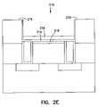
- FIG. 2Eshows the semiconductor structure following the next sequence of processing.
- the residual photoresist layer 212has served as a blocking layer to define the implant areas for the inhibiting layer 214 , and the copper seed layer 216 .
- the residual photoresist layer 212is removed using a wet-strip process.
- the residual photoresist layer 212is removed using a tape lift-off technique.
- the residual photoresist layer 212is removed using a tape lift-off technique in combination with a wet-strip process.
- removing the residual photoresist layer 212includes removing the unwanted copper seed layer 216 , and the unwanted inhibiting layer 214 from a portion of the surface of the wafer. Such a portion of the surface of the wafer may include a number of regions outside of the trench 210 near the vicinity of the top surface 219 .
- the semiconductor structurewill now appear as shown in FIG. 2E .
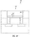
- FIG. 2Fshows the semiconductor structure following the next sequence of processing.
- the semiconductor structure 200includes a copper metallization layer 220 .
- the copper metallization layer 220is selectively formed on the copper seed layer 216 in the trench 210 .
- the copper metallization layer 220includes copper as an element in its composition.
- the copper metallization layer 220is deposited using a selective CVD process.
- depositing the metallization layer 220includes depositing a copper metallization layer 220 using electroplating or electroless plating.
- the semiconductor structure 200is heat-treated at about 250 degrees Celsius to about 350 degrees Celsius from about one to about two hours after the electroplating of the copper.
- wiring structuremeans the inclusion of a contacting and interconnecting structure in an integrated circuit so as to electrically connect various devices together.
- wiring structuremeans the inclusion of at least one copper metallization layer.
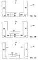
- FIGS. 3A-3Care closed-up cross-sectional views of a semiconductor structure during processing according to one embodiment of the present invention.
- FIG. 3Ashows a closed-up cross-sectional view of a semiconductor structure 300 during processing.
- Semiconductor structure 300includes elements that are similar to elements discussed in FIGS. 2A-2F . The discussion of those elements that are similar and have an identical last-two digit nomenclature is incorporated here in full.
- FIG. 3Aincludes a trench 310 that is defined by the current shape of protective layer 302 , an insulator 308 , and vias 305 A and 305 B.
- the insulator 308includes a first substance.
- the trench 310has been defined to begin the formation of a copper metallization layer. In subsequent processing steps, the trench 310 may be filled with copper to complete the formation of a copper metallization layer. As discussed hereinbefore, the formation of a copper metallization layer into the trench 310 , without the various embodiments of the present invention, may cause the undesired diffusion of copper atoms into the insulator 308 .
- FIG. 3Bshows the next sequence of processing.
- a layer of a second substanceis deposited abutting the insulator layer 308 and the vias 305 A and 305 B.
- the second substanceoccupies a portion of the trench 310 .
- FIG. 3Cshows the next sequence of processing.
- An inhibiting layer 314is formed from the first substance of the insulator 308 and the second substance 398 . This inhibiting layer 314 helps to enhance the copper metallization layer.
- the inhibiting layer 314forms an integral part of the insulator 308 , the inhibiting layer 314 is effective in inhibiting the diffusion of the copper metallization layer.
- the inhibiting layer 314forms an integral part of the semiconductor structure 300 , it scales with each succeeding generation of semiconductor processing technology so as to maintain an effective inhibiting layer against the capacitive-resistive effects.
- the inhibiting layer 314occupies a portion of the space of the insulator 308 but not the space of the trench 310 , more of the space of the trench 310 can be used for the deposition of copper.
- the metallization layer of the described embodimentsis enhanced.
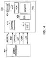
- FIG. 4is a block diagram of a device according to one embodiment of the present invention.
- the memory device 400includes an array of memory cells 402 , address decoder 404 , row access circuitry 406 , column access circuitry 408 , control circuitry 410 , and input/output circuit 412 .
- the memory device 400can be coupled to an external microprocessor 414 , or memory controller for memory accessing.
- the memory device 400receives control signals from the processor 414 , such as WE*, RAS* and CAS* signals.
- the memory device 400is used to store data which is accessed via I/O lines. It will be appreciated by those skilled in the art that additional circuitry and control signals can be provided, and that the memory device 400 has been simplified to help focus on the invention.
- At least one of the memory cellshas an inhibiting layer in accordance with the aforementioned embodiments.
- at least one of the memory cellshas a capacitor and at least one transistor that are interconnected through a semiconductor structure in accordance with the aforementioned
- DRAMDynamic Random Access Memory
- SRAMStatic Random Access Memory
- Flash memoriesOther alternative types of devices include SRAM (Static Random Access Memory) or Flash memories.
- the DRAMcould be a synchronous DRAM commonly referred to as SGRAM (Synchronous Graphics Random Access Memory), SDRAM (Synchronous Dynamic Random Access Memory), SDRAM II, and DDR SDRAM (Double Data Rate SDRAM), as well as Synchlink or Rambus DRAMs and other emerging memory technologies.
- memory devices of the type described hereinare generally fabricated as an integrated circuit containing a variety of semiconductor devices.
- the integrated circuitis supported by a substrate.
- Integrated circuitsare typically repeated multiple times on each substrate.
- the substrateis further processed to separate the integrated circuits into dies as is well known in the art.
- FIG. 5is an elevation view of a semiconductor wafer according to one embodiment of the present invention.
- a semiconductor die 510is produced from a wafer 500 .
- a dieis an individual pattern, typically rectangular, on a substrate that contains circuitry, or integrated circuit devices, to perform a specific function. At least one of the integrated circuit devices includes a memory cell as discussed in the various embodiments heretofore in accordance with the invention.
- a semiconductor waferwill typically contain a repeated pattern of such dies containing the same functionality.
- Die 510may contain circuitry for the inventive memory device, as discussed above. Die 510 may further contain additional circuitry to extend to such complex devices as a monolithic processor with multiple functionality.
- Die 510is typically packaged in a protective casing (not shown) with leads extending therefrom (not shown) providing access to the circuitry of the die for unilateral or bilateral communication and control.
- leads extending therefrom(not shown) providing access to the circuitry of the die for unilateral or bilateral communication and control.
- at least two of the integrated circuit devicesare interconnected through a semiconductor structure as discussed in the aforementioned embodiments.
- FIG. 6is a block diagram of a circuit module according to one embodiment of the present invention.
- Two or more dies 610may be combined, with or without protective casing, into a circuit module 600 to enhance or extend the functionality of an individual die 610 .
- Circuit module 600may be a combination of dies 610 representing a variety of functions, or a combination of dies 610 containing the same functionality.
- One or more dies 610 of circuit module 600contain at least one of the semiconductor structure to enhance a copper metallization layer in accordance with the aforementioned embodiments of the present invention.
- Circuit module 600may be a subcomponent of a variety of electronic systems, such as a clock, a television, a cell phone, a personal computer, an automobile, an industrial control system, an aircraft, and others. Circuit module 600 will have a variety of leads 612 extending therefrom and coupled to the dies 610 providing unilateral or bilateral communication and control.
- FIG. 7is a block diagram of a memory module according to one embodiment of the present invention.
- Memory module 700contains multiple memory devices 710 contained on support 715 , the number depending upon the desired bus width and the desire for parity.
- Memory module 700accepts a command signal from an external controller (not shown) on a command link 720 and provides for data input and data output on data links 730 .
- the command link 720 and data links 730are connected to leads 740 extending from the support 715 .
- Leads 740are shown for conceptual purposes and are not limited to the positions as shown.
- At least one of the memory devices 710includes a memory cell as discussed in various embodiments in accordance with the invention.
- FIG. 8is a block diagram of a system according to one embodiment of the present invention.
- Electronic system 800contains one or more circuit modules 802 .
- Electronic system 800generally contains a user interface 804 .
- User interface 804provides a user of the electronic system 800 with some form of control or observation of the results of the electronic system 800 .
- Some examples of user interface 804include the keyboard, pointing device, monitor, or printer of a personal computer; the tuning dial, display, or speakers of a radio; the ignition switch, gauges, or gas pedal of an automobile; and the card reader, keypad, display, or currency dispenser of an automated teller machine.
- User interface 804may further describe access ports provided to electronic system 800 . Access ports are used to connect an electronic system to the more tangible user interface components previously exemplified.
- One or more of the circuit modules 802may be a processor providing some form of manipulation, control, or direction of inputs from or outputs to user interface 804 , or of other information either preprogrammed into, or otherwise provided to, electronic system 800 .
- electronic system 800will often contain certain mechanical components (not shown) in addition to circuit modules 802 and user interface 804 . It will be appreciated that the one or more circuit modules 802 in electronic system 800 can be replaced by a single integrated circuit.
- electronic system 800may be a subcomponent of a larger electronic system.
- At least one of the circuit modules 802includes at least an integrated circuit that comprises at least two semiconductor devices that are interconnected through a semiconductor structure as discussed in various embodiments in accordance with the invention.
- FIG. 9is a block diagram of a system according to one embodiment of the present invention.
- Memory system 900contains one or more memory modules 902 and a memory controller 912 .
- Each memory module 902includes at least one memory device 910 .
- Memory controller 912provides and controls a bidirectional interface between memory system 900 and an external system bus 920 .
- Memory system 900accepts a command signal from the external bus 920 and relays it to the one or more memory modules 902 on a command link 930 .
- Memory system 900provides for data input and data output between the one or more memory modules 902 and external system bus 920 on data links 940 .
- At least one of the memory devices 910includes a memory cell that includes an inhibiting layer as discussed in various embodiments in accordance with the invention.
- FIG. 10is a block diagram of a system according to one embodiment of the present invention.
- Computer system 1000contains a processor 1010 and a memory system 1002 housed in a computer unit 1005 .
- the processor 1010may contain at least two semiconductor devices that are interconnected through a semiconductor structure as described hereintofore.
- Computer system 1000is but one example of an electronic system containing another electronic system, e.g., memory system 1002 , as a subcomponent.
- the memory system 1002may include a memory cell as discussed in various embodiments of the present invention.
- Computer system 1000optionally contains user interface components. These user interface components include a keyboard 1020 , a pointing device 1030 , a monitor 1040 , a printer 1050 , and a bulk storage device 1060 .
- processor 1010 and memory system 1002 of computer system 1000can be incorporated on a single integrated circuit. Such single-package processing units reduce the communication time between the processor and the memory circuit.
Landscapes
- Engineering & Computer Science (AREA)
- Physics & Mathematics (AREA)
- Condensed Matter Physics & Semiconductors (AREA)
- General Physics & Mathematics (AREA)
- Computer Hardware Design (AREA)
- Microelectronics & Electronic Packaging (AREA)
- Power Engineering (AREA)
- Manufacturing & Machinery (AREA)
- Plasma & Fusion (AREA)
- Internal Circuitry In Semiconductor Integrated Circuit Devices (AREA)
Abstract
Description
Claims (37)
Priority Applications (5)
| Application Number | Priority Date | Filing Date | Title |
|---|---|---|---|
| US10/196,081US7378737B2 (en) | 2000-01-18 | 2002-07-16 | Structures and methods to enhance copper metallization |
| US10/854,552US8779596B2 (en) | 2000-01-18 | 2004-05-26 | Structures and methods to enhance copper metallization |
| US11/458,195US7535103B2 (en) | 2000-01-18 | 2006-07-18 | Structures and methods to enhance copper metallization |
| US12/467,889US20090243106A1 (en) | 2000-01-18 | 2009-05-18 | Structures and methods to enhance copper metallization |
| US14/183,325US20140159241A1 (en) | 2000-01-18 | 2014-02-18 | Structures and Methods to Enhance Copper Metallization |
Applications Claiming Priority (2)
| Application Number | Priority Date | Filing Date | Title |
|---|---|---|---|
| US09/483,869US6420262B1 (en) | 2000-01-18 | 2000-01-18 | Structures and methods to enhance copper metallization |
| US10/196,081US7378737B2 (en) | 2000-01-18 | 2002-07-16 | Structures and methods to enhance copper metallization |
Related Parent Applications (1)
| Application Number | Title | Priority Date | Filing Date |
|---|---|---|---|
| US09/483,869DivisionUS6420262B1 (en) | 2000-01-18 | 2000-01-18 | Structures and methods to enhance copper metallization |
Related Child Applications (1)
| Application Number | Title | Priority Date | Filing Date |
|---|---|---|---|
| US10/854,552DivisionUS8779596B2 (en) | 2000-01-18 | 2004-05-26 | Structures and methods to enhance copper metallization |
Publications (2)
| Publication Number | Publication Date |
|---|---|
| US20020182859A1 US20020182859A1 (en) | 2002-12-05 |
| US7378737B2true US7378737B2 (en) | 2008-05-27 |
Family
ID=23921827
Family Applications (8)
| Application Number | Title | Priority Date | Filing Date |
|---|---|---|---|
| US09/483,869Expired - LifetimeUS6420262B1 (en) | 2000-01-18 | 2000-01-18 | Structures and methods to enhance copper metallization |
| US10/195,965Expired - LifetimeUS7301190B2 (en) | 2000-01-18 | 2002-07-16 | Structures and methods to enhance copper metallization |
| US10/196,081Expired - Fee RelatedUS7378737B2 (en) | 2000-01-18 | 2002-07-16 | Structures and methods to enhance copper metallization |
| US10/196,078Expired - LifetimeUS6743716B2 (en) | 2000-01-18 | 2002-07-16 | Structures and methods to enhance copper metallization |
| US10/854,552Expired - Fee RelatedUS8779596B2 (en) | 2000-01-18 | 2004-05-26 | Structures and methods to enhance copper metallization |
| US11/458,195Expired - LifetimeUS7535103B2 (en) | 2000-01-18 | 2006-07-18 | Structures and methods to enhance copper metallization |
| US12/467,889AbandonedUS20090243106A1 (en) | 2000-01-18 | 2009-05-18 | Structures and methods to enhance copper metallization |
| US14/183,325AbandonedUS20140159241A1 (en) | 2000-01-18 | 2014-02-18 | Structures and Methods to Enhance Copper Metallization |
Family Applications Before (2)
| Application Number | Title | Priority Date | Filing Date |
|---|---|---|---|
| US09/483,869Expired - LifetimeUS6420262B1 (en) | 2000-01-18 | 2000-01-18 | Structures and methods to enhance copper metallization |
| US10/195,965Expired - LifetimeUS7301190B2 (en) | 2000-01-18 | 2002-07-16 | Structures and methods to enhance copper metallization |
Family Applications After (5)
| Application Number | Title | Priority Date | Filing Date |
|---|---|---|---|
| US10/196,078Expired - LifetimeUS6743716B2 (en) | 2000-01-18 | 2002-07-16 | Structures and methods to enhance copper metallization |
| US10/854,552Expired - Fee RelatedUS8779596B2 (en) | 2000-01-18 | 2004-05-26 | Structures and methods to enhance copper metallization |
| US11/458,195Expired - LifetimeUS7535103B2 (en) | 2000-01-18 | 2006-07-18 | Structures and methods to enhance copper metallization |
| US12/467,889AbandonedUS20090243106A1 (en) | 2000-01-18 | 2009-05-18 | Structures and methods to enhance copper metallization |
| US14/183,325AbandonedUS20140159241A1 (en) | 2000-01-18 | 2014-02-18 | Structures and Methods to Enhance Copper Metallization |
Country Status (1)
| Country | Link |
|---|---|
| US (8) | US6420262B1 (en) |
Cited By (5)
| Publication number | Priority date | Publication date | Assignee | Title |
|---|---|---|---|---|
| US20060006548A1 (en)* | 2003-08-05 | 2006-01-12 | Micron Technology, Inc. | H2 plasma treatment |
| US7535103B2 (en) | 2000-01-18 | 2009-05-19 | Micron Technology, Inc. | Structures and methods to enhance copper metallization |
| US8525339B2 (en) | 2011-07-27 | 2013-09-03 | International Business Machines Corporation | Hybrid copper interconnect structure and method of fabricating same |
| US8796853B2 (en) | 2012-02-24 | 2014-08-05 | International Business Machines Corporation | Metallic capped interconnect structure with high electromigration resistance and low resistivity |
| US9312203B2 (en) | 2013-01-02 | 2016-04-12 | Globalfoundries Inc. | Dual damascene structure with liner |
Families Citing this family (53)
| Publication number | Priority date | Publication date | Assignee | Title |
|---|---|---|---|---|
| US6429120B1 (en) | 2000-01-18 | 2002-08-06 | Micron Technology, Inc. | Methods and apparatus for making integrated-circuit wiring from copper, silver, gold, and other metals |
| US6284316B1 (en)* | 1998-02-25 | 2001-09-04 | Micron Technology, Inc. | Chemical vapor deposition of titanium |
| US6376374B1 (en)* | 1998-05-12 | 2002-04-23 | Semitool, Inc. | Process and manufacturing tool architecture for use in the manufacturing of one or more protected metallization structures on a workpiece |
| US6495442B1 (en)* | 2000-10-18 | 2002-12-17 | Magic Corporation | Post passivation interconnection schemes on top of the IC chips |
| US7276788B1 (en) | 1999-08-25 | 2007-10-02 | Micron Technology, Inc. | Hydrophobic foamed insulators for high density circuits |
| US7262130B1 (en)* | 2000-01-18 | 2007-08-28 | Micron Technology, Inc. | Methods for making integrated-circuit wiring from copper, silver, gold, and other metals |
| US7211512B1 (en) | 2000-01-18 | 2007-05-01 | Micron Technology, Inc. | Selective electroless-plated copper metallization |
| US6376370B1 (en)* | 2000-01-18 | 2002-04-23 | Micron Technology, Inc. | Process for providing seed layers for using aluminum, copper, gold and silver metallurgy process for providing seed layers for using aluminum, copper, gold and silver metallurgy |
| US6413827B2 (en) | 2000-02-14 | 2002-07-02 | Paul A. Farrar | Low dielectric constant shallow trench isolation |
| US6677209B2 (en) | 2000-02-14 | 2004-01-13 | Micron Technology, Inc. | Low dielectric constant STI with SOI devices |
| US6890847B1 (en)* | 2000-02-22 | 2005-05-10 | Micron Technology, Inc. | Polynorbornene foam insulation for integrated circuits |
| US6511912B1 (en)* | 2000-08-22 | 2003-01-28 | Micron Technology, Inc. | Method of forming a non-conformal layer over and exposing a trench |
| US6657303B1 (en)* | 2000-12-18 | 2003-12-02 | Advanced Micro Devices, Inc. | Integrated circuit with low solubility metal-conductor interconnect cap |
| US6835655B1 (en) | 2001-11-26 | 2004-12-28 | Advanced Micro Devices, Inc. | Method of implanting copper barrier material to improve electrical performance |
| US6703307B2 (en) | 2001-11-26 | 2004-03-09 | Advanced Micro Devices, Inc. | Method of implantation after copper seed deposition |
| US6703308B1 (en) | 2001-11-26 | 2004-03-09 | Advanced Micro Devices, Inc. | Method of inserting alloy elements to reduce copper diffusion and bulk diffusion |
| US7696092B2 (en) | 2001-11-26 | 2010-04-13 | Globalfoundries Inc. | Method of using ternary copper alloy to obtain a low resistance and large grain size interconnect |
| US7115498B1 (en)* | 2002-04-16 | 2006-10-03 | Advanced Micro Devices, Inc. | Method of ultra-low energy ion implantation to form alloy layers in copper |
| US6861349B1 (en) | 2002-05-15 | 2005-03-01 | Advanced Micro Devices, Inc. | Method of forming an adhesion layer with an element reactive with a barrier layer |
| US7074709B2 (en)* | 2002-06-28 | 2006-07-11 | Texas Instruments Incorporated | Localized doping and/or alloying of metallization for increased interconnect performance |
| US6903001B2 (en)* | 2002-07-18 | 2005-06-07 | Micron Technology Inc. | Techniques to create low K ILD for BEOL |
| KR100897505B1 (en)* | 2002-11-19 | 2009-05-15 | 삼성전자주식회사 | Thin film transistor substrate of liquid crystal display device and manufacturing method thereof |
| US7192892B2 (en) | 2003-03-04 | 2007-03-20 | Micron Technology, Inc. | Atomic layer deposited dielectric layers |
| US6740392B1 (en) | 2003-04-15 | 2004-05-25 | Micron Technology, Inc. | Surface barriers for copper and silver interconnects produced by a damascene process |
| US7169706B2 (en)* | 2003-10-16 | 2007-01-30 | Advanced Micro Devices, Inc. | Method of using an adhesion precursor layer for chemical vapor deposition (CVD) copper deposition |
| FR2863405B1 (en)* | 2003-12-08 | 2006-02-03 | Commissariat Energie Atomique | MOLECULAR BONDING OF MICROELECTRONIC COMPONENTS ON A POLYMERIC FILM |
| US20050137882A1 (en)* | 2003-12-17 | 2005-06-23 | Cameron Don T. | Method for authenticating goods |
| US7390551B2 (en)* | 2004-07-02 | 2008-06-24 | Caterpillar Inc. | System and method for encapsulation and protection of components |
| EP1722219A1 (en)* | 2005-05-10 | 2006-11-15 | Sumitomo Electric Industries, Ltd. | Gas sensor |
| US7927948B2 (en) | 2005-07-20 | 2011-04-19 | Micron Technology, Inc. | Devices with nanocrystals and methods of formation |
| JP4778765B2 (en)* | 2005-10-07 | 2011-09-21 | 富士通セミコンダクター株式会社 | Semiconductor device and manufacturing method thereof |
| US7601604B2 (en)* | 2006-10-12 | 2009-10-13 | Atmel Corporation | Method for fabricating conducting plates for a high-Q MIM capacitor |
| KR100829385B1 (en)* | 2006-11-27 | 2008-05-13 | 동부일렉트로닉스 주식회사 | Semiconductor device and method of manufacturing the same |
| US20080173975A1 (en)* | 2007-01-22 | 2008-07-24 | International Business Machines Corporation | Programmable resistor, switch or vertical memory cell |
| SG149807A1 (en)* | 2007-07-30 | 2009-02-27 | Stats Chippac Ltd | Semiconductor device and method of providing common voltage bus and wire bondable redistribution |
| US7859025B2 (en)* | 2007-12-06 | 2010-12-28 | International Business Machines Corporation | Metal ion transistor |
| US20090166864A1 (en)* | 2007-12-28 | 2009-07-02 | Mengzhi Pang | Method to prevent copper migration in a semiconductor package |
| US20100249700A1 (en)* | 2009-03-27 | 2010-09-30 | Ethicon Endo-Surgery, Inc. | Surgical instruments for in vivo assembly |
| US8410575B2 (en)* | 2010-03-30 | 2013-04-02 | Infineon Technologies Austria Ag | High voltage semiconductor devices and methods of forming the same |
| US8703602B2 (en)* | 2010-12-02 | 2014-04-22 | Qualcomm Incorporated | Selective seed layer treatment for feature plating |
| US8941182B2 (en)* | 2011-06-07 | 2015-01-27 | Globalfoundries Inc. | Buried sublevel metallizations for improved transistor density |
| US8564132B2 (en)* | 2011-08-17 | 2013-10-22 | International Business Machines Corporation | Tungsten metallization: structure and fabrication of same |
| US9123784B2 (en)* | 2012-08-21 | 2015-09-01 | Nanya Technology Corporation | Memory process and memory structure made thereby |
| US9030013B2 (en)* | 2012-09-21 | 2015-05-12 | Taiwan Semiconductor Manufacturing Company, Ltd. | Interconnect structures comprising flexible buffer layers |
| US8816500B2 (en)* | 2012-12-14 | 2014-08-26 | Infineon Technologies Ag | Semiconductor device having peripheral polymer structures |
| US9202743B2 (en) | 2012-12-17 | 2015-12-01 | International Business Machines Corporation | Graphene and metal interconnects |
| US9293412B2 (en) | 2012-12-17 | 2016-03-22 | International Business Machines Corporation | Graphene and metal interconnects with reduced contact resistance |
| US9431346B2 (en) | 2013-04-30 | 2016-08-30 | GlobalFoundries, Inc. | Graphene-metal E-fuse |
| US9257391B2 (en)* | 2013-04-30 | 2016-02-09 | GlobalFoundries, Inc. | Hybrid graphene-metal interconnect structures |
| US9263325B1 (en) | 2014-08-20 | 2016-02-16 | Globalfoundries Inc. | Precut metal lines |
| US9508642B2 (en)* | 2014-08-20 | 2016-11-29 | Globalfoundries Inc. | Self-aligned back end of line cut |
| FR3033929B1 (en)* | 2015-03-17 | 2017-03-31 | Labinal Power Systems | ELECTRICAL CABLE FOR THE POWER SUPPLY OF ELECTRICAL EQUIPMENT |
| CN111969061B (en)* | 2020-08-12 | 2024-06-04 | 无锡先仁智芯微电子技术有限公司 | LDMOS structure and manufacturing method thereof |
Citations (255)
| Publication number | Priority date | Publication date | Assignee | Title |
|---|---|---|---|---|
| US2842438A (en) | 1956-08-02 | 1958-07-08 | American Metal Climax Inc | Copper-zirconium alloys |
| US3515663A (en) | 1968-02-01 | 1970-06-02 | Hewlett Packard Co | Triode sputtering apparatus using an electron emitter |
| US3954570A (en) | 1974-11-11 | 1976-05-04 | Amp Incorporated | Sensitized polyimides and circuit elements thereof |
| US4213818A (en) | 1979-01-04 | 1980-07-22 | Signetics Corporation | Selective plasma vapor etching process |
| US4386116A (en) | 1981-12-24 | 1983-05-31 | International Business Machines Corporation | Process for making multilayer integrated circuit substrate |
| US4394223A (en) | 1981-10-06 | 1983-07-19 | The United States Of America As Represented By The Secretary Of The Air Force | Tin and gold plating process |
| US4423547A (en) | 1981-06-01 | 1984-01-03 | International Business Machines Corporation | Method for forming dense multilevel interconnection metallurgy for semiconductor devices |
| US4565157A (en) | 1983-03-29 | 1986-01-21 | Genus, Inc. | Method and apparatus for deposition of tungsten silicides |
| US4574095A (en) | 1984-11-19 | 1986-03-04 | International Business Machines Corporation | Selective deposition of copper |
| US4762728A (en) | 1985-04-09 | 1988-08-09 | Fairchild Semiconductor Corporation | Low temperature plasma nitridation process and applications of nitride films formed thereby |
| US4788082A (en) | 1984-02-13 | 1988-11-29 | Schmitt Jerome J | Method and apparatus for the deposition of solid films of a material from a jet stream entraining the gaseous phase of said material |
| US4824544A (en) | 1987-10-29 | 1989-04-25 | International Business Machines Corporation | Large area cathode lift-off sputter deposition device |
| US4847111A (en) | 1988-06-30 | 1989-07-11 | Hughes Aircraft Company | Plasma-nitridated self-aligned tungsten system for VLSI interconnections |
| US4931410A (en) | 1987-08-25 | 1990-06-05 | Hitachi, Ltd. | Process for producing semiconductor integrated circuit device having copper interconnections and/or wirings, and device produced |
| US4933743A (en) | 1989-03-11 | 1990-06-12 | Fairchild Semiconductor Corporation | High performance interconnect system for an integrated circuit |
| US4948459A (en) | 1988-01-20 | 1990-08-14 | U.S. Philips Corporation | Method of enabling electrical connection to a substructure forming part of an electronic device |
| US4962058A (en) | 1989-04-14 | 1990-10-09 | International Business Machines Corporation | Process for fabricating multi-level integrated circuit wiring structure from a single metal deposit |
| US4990229A (en) | 1989-06-13 | 1991-02-05 | Plasma & Materials Technologies, Inc. | High density plasma deposition and etching apparatus |
| US4996584A (en) | 1985-01-31 | 1991-02-26 | Gould, Inc. | Thin-film electrical connections for integrated circuits |
| US5019531A (en) | 1988-05-23 | 1991-05-28 | Nippon Telegraph And Telephone Corporation | Process for selectively growing thin metallic film of copper or gold |
| US5034799A (en) | 1989-02-22 | 1991-07-23 | Kabushiki Kaisha Toshiba | Semiconductor integrated circuit device having a hollow multi-layered lead structure |
| US5071518A (en) | 1989-10-24 | 1991-12-10 | Microelectronics And Computer Technology Corporation | Method of making an electrical multilayer interconnect |
| US5084412A (en) | 1989-10-02 | 1992-01-28 | Kabushiki Kaisha Toshiba | Method of manufacturing a semiconductor device with a copper wiring layer |
| US5100499A (en) | 1989-12-20 | 1992-03-31 | Texas Instruments Incorporated | Copper dry etch process using organic and amine radicals |
| US5130274A (en) | 1991-04-05 | 1992-07-14 | International Business Machines Corporation | Copper alloy metallurgies for VLSI interconnection structures |
| US5149615A (en) | 1991-01-08 | 1992-09-22 | The Boeing Company | Method for producing a planar surface on which a conductive layer can be applied |
| US5158986A (en) | 1991-04-05 | 1992-10-27 | Massachusetts Institute Of Technology | Microcellular thermoplastic foamed with supercritical fluid |
| US5171712A (en) | 1991-12-20 | 1992-12-15 | Vlsi Technology, Inc. | Method of constructing termination electrodes on yielded semiconductor die by visibly aligning the die pads through a transparent substrate |
| US5173442A (en) | 1990-07-23 | 1992-12-22 | Microelectronics And Computer Technology Corporation | Methods of forming channels and vias in insulating layers |
| JPH05160826A (en) | 1991-12-04 | 1993-06-25 | Mitsubishi Electric Corp | Frame synchronization method |
| US5231056A (en) | 1992-01-15 | 1993-07-27 | Micron Technology, Inc. | Tungsten silicide (WSix) deposition process for semiconductor manufacture |
| US5240878A (en) | 1991-04-26 | 1993-08-31 | International Business Machines Corporation | Method for forming patterned films on a substrate |
| US5243222A (en) | 1991-04-05 | 1993-09-07 | International Business Machines Corporation | Copper alloy metallurgies for VLSI interconnection structures |
| JPH05267643A (en) | 1992-03-19 | 1993-10-15 | Fujitsu Ltd | Semiconductor device and manufacturing method thereof |
| US5256205A (en) | 1990-05-09 | 1993-10-26 | Jet Process Corporation | Microwave plasma assisted supersonic gas jet deposition of thin film materials |
| JPH05295533A (en) | 1992-04-17 | 1993-11-09 | Sony Corp | Film forming method and film forming device using electron cyclotron resonance |
| US5348811A (en) | 1986-07-25 | 1994-09-20 | Fuji Photo Film Co., Ltd. | Recording medium and method of performing recording/producing on the recording medium |
| US5354712A (en) | 1992-11-12 | 1994-10-11 | Northern Telecom Limited | Method for forming interconnect structures for integrated circuits |
| US5371042A (en) | 1992-06-16 | 1994-12-06 | Applied Materials, Inc. | Method of filling contacts in semiconductor devices |
| US5374849A (en) | 1992-03-02 | 1994-12-20 | Mitsubishi Denki Kabushiki Kaisha | Conductive layer connection structure of semiconductor device |
| US5384284A (en) | 1993-10-01 | 1995-01-24 | Micron Semiconductor, Inc. | Method to form a low resistant bond pad interconnect |
| US5401680A (en) | 1992-02-18 | 1995-03-28 | National Semiconductor Corporation | Method for forming a ceramic oxide capacitor having barrier layers |
| US5413687A (en) | 1991-11-27 | 1995-05-09 | Rogers Corporation | Method for metallizing fluoropolymer substrates |
| US5426330A (en) | 1992-02-26 | 1995-06-20 | International Business Machines Corporation | Refractory metal capped low resistivity metal conductor lines and vias |
| US5442237A (en) | 1991-10-21 | 1995-08-15 | Motorola Inc. | Semiconductor device having a low permittivity dielectric |
| JPH0778815B2 (en) | 1986-09-19 | 1995-08-23 | 富士通株式会社 | Voting ticket automatic refund machine |
| US5447887A (en) | 1994-04-01 | 1995-09-05 | Motorola, Inc. | Method for capping copper in semiconductor devices |
| US5451804A (en) | 1994-05-11 | 1995-09-19 | United Microelectronics Corporation | VLSI device with global planarization |
| US5461243A (en) | 1993-10-29 | 1995-10-24 | International Business Machines Corporation | Substrate for tensilely strained semiconductor |
| US5470789A (en) | 1993-03-19 | 1995-11-28 | Fujitsu Limited | Process for fabricating integrated circuit devices |
| US5470801A (en) | 1993-06-28 | 1995-11-28 | Lsi Logic Corporation | Low dielectric constant insulation layer for integrated circuit structure and method of making same |
| JPH07321111A (en) | 1994-05-26 | 1995-12-08 | Meidensha Corp | Method of forming electroless plated interconnection for integrated circuit |
| US5476817A (en) | 1994-05-31 | 1995-12-19 | Texas Instruments Incorporated | Method of making reliable metal leads in high speed LSI semiconductors using both dummy leads and thermoconductive layers |
| US5495667A (en) | 1994-11-07 | 1996-03-05 | Micron Technology, Inc. | Method for forming contact pins for semiconductor dice and interconnects |
| US5506449A (en) | 1993-03-24 | 1996-04-09 | Kawasaki Steel Corporation | Interconnection structure for semiconductor integrated circuit and manufacture of the same |
| US5529956A (en) | 1991-07-23 | 1996-06-25 | Nec Corporation | Multi-layer wiring structure in semiconductor device and method for manufacturing the same |
| US5538922A (en) | 1991-06-03 | 1996-07-23 | Motorola, Inc. | Method for forming contact to a semiconductor device |
| US5539060A (en) | 1993-07-30 | 1996-07-23 | Nippon Zeon Co., Ltd. | Method for hydrogenation of metathesis polymers |
| US5595937A (en) | 1995-04-13 | 1997-01-21 | Nec Corporation | Method for fabricating semiconductor device with interconnections buried in trenches |
| US5609721A (en) | 1994-03-11 | 1997-03-11 | Fujitsu Limited | Semiconductor device manufacturing apparatus and its cleaning method |
| US5625233A (en) | 1995-01-13 | 1997-04-29 | Ibm Corporation | Thin film multi-layer oxygen diffusion barrier consisting of refractory metal, refractory metal aluminide, and aluminum oxide |
| US5625232A (en) | 1994-07-15 | 1997-04-29 | Texas Instruments Incorporated | Reliability of metal leads in high speed LSI semiconductors using dummy vias |
| US5633200A (en) | 1996-05-24 | 1997-05-27 | Micron Technology, Inc. | Process for manufacturing a large grain tungsten nitride film and process for manufacturing a lightly nitrided titanium salicide diffusion barrier with a large grain tungsten nitride cover layer |
| US5635253A (en) | 1994-08-30 | 1997-06-03 | International Business Machines Corporation | Method of replenishing electroless gold plating baths |
| US5635423A (en) | 1994-10-11 | 1997-06-03 | Advanced Micro Devices, Inc. | Simplified dual damascene process for multi-level metallization and interconnection structure |
| US5654245A (en) | 1993-03-23 | 1997-08-05 | Sharp Microelectronics Technology, Inc. | Implantation of nucleating species for selective metallization and products thereof |
| US5662788A (en) | 1996-06-03 | 1997-09-02 | Micron Technology, Inc. | Method for forming a metallization layer |
| US5670420A (en) | 1994-12-05 | 1997-09-23 | Hyundai Electronics Industries Co., Ltd. | Method of forming metal interconnection layer of semiconductor device |
| US5674787A (en) | 1996-01-16 | 1997-10-07 | Sematech, Inc. | Selective electroless copper deposited interconnect plugs for ULSI applications |
| US5679608A (en) | 1994-12-21 | 1997-10-21 | Advanced Micro Devices, Inc. | Processing techniques for achieving production-worthy, low dielectric, low dielectric, low interconnect resistance and high performance IC |
| US5681441A (en) | 1992-12-22 | 1997-10-28 | Elf Technologies, Inc. | Method for electroplating a substrate containing an electroplateable pattern |
| EP0808915A2 (en) | 1996-05-23 | 1997-11-26 | Applied Materials, Inc. | Chemical vapor deposition and sputtering method and apparatus |
| US5693563A (en) | 1996-07-15 | 1997-12-02 | Chartered Semiconductor Manufacturing Pte Ltd. | Etch stop for copper damascene process |
| US5695810A (en) | 1996-11-20 | 1997-12-09 | Cornell Research Foundation, Inc. | Use of cobalt tungsten phosphide as a barrier material for copper metallization |
| US5719089A (en) | 1996-06-21 | 1998-02-17 | Vanguard International Semiconductor Corporation | Method for etching polymer-assisted reduced small contacts for ultra large scale integration semiconductor devices |
| US5719410A (en) | 1993-12-28 | 1998-02-17 | Kabushiki Kaisha Toshiba | Semiconductor device wiring or electrode |
| US5719447A (en) | 1993-06-03 | 1998-02-17 | Intel Corporation | Metal alloy interconnections for integrated circuits |
| US5739579A (en) | 1992-06-29 | 1998-04-14 | Intel Corporation | Method for forming interconnections for semiconductor fabrication and semiconductor device having such interconnections |
| US5763953A (en) | 1993-01-05 | 1998-06-09 | Kabushiki Kaisha Toshiba | Semiconductor device and method of manufacturing the same |
| US5780358A (en) | 1996-04-08 | 1998-07-14 | Chartered Semiconductor Manufacturing Ltd. | Method for chemical-mechanical polish (CMP) planarizing of cooper containing conductor layers |
| US5785570A (en) | 1994-07-26 | 1998-07-28 | Pixtech S.A. | Anode for a flat display screen |
| US5789264A (en) | 1996-03-27 | 1998-08-04 | Daewoo Electronics Co., Ltd. | Method for manufacturing a thin film actuated mirror having a flat light reflecting surface |
| US5792522A (en) | 1996-09-18 | 1998-08-11 | Intel Corporation | High density plasma physical vapor deposition |
| US5801098A (en) | 1996-09-03 | 1998-09-01 | Motorola, Inc. | Method of decreasing resistivity in an electrically conductive layer |
| US5814557A (en) | 1996-05-20 | 1998-09-29 | Motorola, Inc. | Method of forming an interconnect structure |
| US5821168A (en) | 1997-07-16 | 1998-10-13 | Motorola, Inc. | Process for forming a semiconductor device |
| US5824599A (en) | 1996-01-16 | 1998-10-20 | Cornell Research Foundation, Inc. | Protected encapsulation of catalytic layer for electroless copper interconnect |
| US5840625A (en) | 1995-03-30 | 1998-11-24 | Siemens Aktiengesellschaft | Method of fabricating integrated circuit interconnection employing tungsten/aluminum layers |
| US5858877A (en) | 1992-07-28 | 1999-01-12 | Micron Technology, Inc. | Self-aligned process for making contacts to silicon substrates during the manufacture of integrated circuits therein |
| US5891797A (en) | 1997-10-20 | 1999-04-06 | Micron Technology, Inc. | Method of forming a support structure for air bridge wiring of an integrated circuit |
| US5891804A (en) | 1996-04-18 | 1999-04-06 | Texas Instruments Incorporated | Process for conductors with selective deposition |
| US5893752A (en) | 1997-12-22 | 1999-04-13 | Motorola, Inc. | Process for forming a semiconductor device |
| US5895740A (en) | 1996-11-13 | 1999-04-20 | Vanguard International Semiconductor Corp. | Method of forming contact holes of reduced dimensions by using in-situ formed polymeric sidewall spacers |
| US5897370A (en) | 1994-08-05 | 1999-04-27 | International Business Machines Corporation | High aspect ratio low resistivity lines/vias by surface diffusion |
| US5899740A (en) | 1997-03-04 | 1999-05-04 | Samsung Electronics Co., Ltd. | Methods of fabricating copper interconnects for integrated circuits |
| US5907772A (en) | 1996-02-26 | 1999-05-25 | Nec Corporation | Method of producing cylindrical storage node of stacked capacitor in memory cell |
| US5911113A (en) | 1997-03-18 | 1999-06-08 | Applied Materials, Inc. | Silicon-doped titanium wetting layer for aluminum plug |
| US5913147A (en) | 1997-01-21 | 1999-06-15 | Advanced Micro Devices, Inc. | Method for fabricating copper-aluminum metallization |
| US5925930A (en) | 1996-05-21 | 1999-07-20 | Micron Technology, Inc. | IC contacts with palladium layer and flexible conductive epoxy bumps |
| US5930669A (en)* | 1997-04-03 | 1999-07-27 | International Business Machines Corporation | Continuous highly conductive metal wiring structures and method for fabricating the same |
| US5932928A (en) | 1997-07-03 | 1999-08-03 | Micron Technology, Inc. | Semiconductor circuit interconnections and methods of making such interconnections |
| US5933758A (en) | 1997-05-12 | 1999-08-03 | Motorola, Inc. | Method for preventing electroplating of copper on an exposed surface at the edge exclusion of a semiconductor wafer |
| US5937320A (en) | 1998-04-08 | 1999-08-10 | International Business Machines Corporation | Barrier layers for electroplated SnPb eutectic solder joints |
| US5940733A (en) | 1995-05-03 | 1999-08-17 | Applied Materials, Inc. | Method of making polysilicon/tungsten silicide multilayer composite on an integrated circuit structure |
| US5939771A (en) | 1995-10-30 | 1999-08-17 | Nec Corporation | Semiconductor device having an organic resin layer and silicon oxide layer containing fluorine for preventing crosstalk between metal lines and a method of manufacturing the same |
| US5948467A (en) | 1998-07-24 | 1999-09-07 | Sharp Laboratories Of America, Inc. | Enhanced CVD copper adhesion by two-step deposition process |
| US5962923A (en) | 1995-08-07 | 1999-10-05 | Applied Materials, Inc. | Semiconductor device having a low thermal budget metal filling and planarization of contacts, vias and trenches |
| US5969398A (en) | 1997-08-07 | 1999-10-19 | Mitsubishi Denki Kabushiki Kaisha | Method for producing a semiconductor device and a semiconductor device |
| US5968327A (en) | 1997-04-14 | 1999-10-19 | Anelva Corporation | Ionizing sputter device using a coil shield |
| US5969422A (en) | 1997-05-15 | 1999-10-19 | Advanced Micro Devices, Inc. | Plated copper interconnect structure |
| US5968333A (en) | 1998-04-07 | 1999-10-19 | Advanced Micro Devices, Inc. | Method of electroplating a copper or copper alloy interconnect |
| US5972179A (en) | 1997-09-30 | 1999-10-26 | Lucent Technologies Inc. | Silicon IC contacts using composite TiN barrier layer |
| US5972804A (en) | 1997-08-05 | 1999-10-26 | Motorola, Inc. | Process for forming a semiconductor device |
| US5976710A (en) | 1991-08-05 | 1999-11-02 | International Business Machines Corporation | Low TCE polyimides as improved insulator in multilayer interconnect structures |
| US5981350A (en) | 1998-05-29 | 1999-11-09 | Micron Technology, Inc. | Method for forming high capacitance memory cells |
| US5985762A (en) | 1997-05-19 | 1999-11-16 | International Business Machines Corporation | Method of forming a self-aligned copper diffusion barrier in vias |
| US5985759A (en) | 1998-02-24 | 1999-11-16 | Applied Materials, Inc. | Oxygen enhancement of ion metal plasma (IMP) sputter deposited barrier layers |
| US5989623A (en) | 1997-08-19 | 1999-11-23 | Applied Materials, Inc. | Dual damascene metallization |
| US6001730A (en) | 1997-10-20 | 1999-12-14 | Motorola, Inc. | Chemical mechanical polishing (CMP) slurry for polishing copper interconnects which use tantalum-based barrier layers |
| US6002175A (en) | 1995-10-05 | 1999-12-14 | Mitsubishi Denki Kabushiki Kaisha | Semiconductor device with improved connection hole for embedding an electrically conductive layer portion |
| US6001736A (en)* | 1995-03-02 | 1999-12-14 | Kawasaki Steel Corporation | Method of manufacturing semiconductor device and an apparatus for manufacturing the same |
| US6004884A (en) | 1996-02-15 | 1999-12-21 | Lam Research Corporation | Methods and apparatus for etching semiconductor wafers |
| US6008117A (en) | 1996-03-29 | 1999-12-28 | Texas Instruments Incorporated | Method of forming diffusion barriers encapsulating copper |
| US6015465A (en) | 1998-04-08 | 2000-01-18 | Applied Materials, Inc. | Temperature control system for semiconductor process chamber |
| US6017820A (en) | 1998-07-17 | 2000-01-25 | Cutek Research, Inc. | Integrated vacuum and plating cluster system |
| EP0304046B1 (en) | 1987-08-19 | 2000-01-26 | Fujitsu Limited | A method of stripping a resist mask |
| US6022802A (en) | 1999-03-18 | 2000-02-08 | Taiwan Semiconductor Manufacturing Company | Low dielectric constant intermetal dielectric (IMD) by formation of air gap between metal lines |
| US6028362A (en) | 1997-05-12 | 2000-02-22 | Yamaha Corporation | Damascene wiring with flat surface |
| US6030877A (en) | 1997-10-06 | 2000-02-29 | Industrial Technology Research Institute | Electroless gold plating method for forming inductor structures |
| US6030895A (en) | 1995-01-03 | 2000-02-29 | International Business Machines Corporation | Method of making a soft metal conductor |
| US6037664A (en) | 1997-08-20 | 2000-03-14 | Sematech Inc | Dual damascene interconnect structure using low dielectric constant material for an inter-level dielectric layer |
| US6037248A (en) | 1997-06-13 | 2000-03-14 | Micron Technology, Inc. | Method of fabricating integrated circuit wiring with low RC time delay |
| US6054172A (en) | 1997-08-22 | 2000-04-25 | Micron Technology, Inc. | Copper electroless deposition on a titanium-containing surface |
| US6054398A (en) | 1999-05-14 | 2000-04-25 | Advanced Micro Devices, Inc. | Semiconductor interconnect barrier for fluorinated dielectrics |
| US6065424A (en) | 1995-12-19 | 2000-05-23 | Cornell Research Foundation, Inc. | Electroless deposition of metal films with spray processor |
| US6069068A (en) | 1997-05-30 | 2000-05-30 | International Business Machines Corporation | Sub-quarter-micron copper interconnections with improved electromigration resistance and reduced defect sensitivity |
| US6071810A (en) | 1996-12-24 | 2000-06-06 | Kabushiki Kaisha Toshiba | Method of filling contact holes and wiring grooves of a semiconductor device |
| US6077792A (en) | 1997-07-14 | 2000-06-20 | Micron Technology, Inc. | Method of forming foamed polymeric material for an integrated circuit |
| US6103320A (en) | 1998-03-05 | 2000-08-15 | Shincron Co., Ltd. | Method for forming a thin film of a metal compound by vacuum deposition |
| US6107186A (en) | 1999-01-27 | 2000-08-22 | Advanced Micro Devices, Inc. | High planarity high-density in-laid metallization patterns by damascene-CMP processing |
| US6117781A (en) | 1999-04-22 | 2000-09-12 | Advanced Micro Devices, Inc. | Optimized trench/via profile for damascene processing |
| US6117782A (en) | 1999-04-22 | 2000-09-12 | Advanced Micro Devices, Inc. | Optimized trench/via profile for damascene filling |
| US6121149A (en) | 1999-04-22 | 2000-09-19 | Advanced Micro Devices, Inc. | Optimized trench/via profile for damascene filling |
| US6120641A (en) | 1998-05-12 | 2000-09-19 | Semitool, Inc. | Process architecture and manufacturing tool sets employing hard mask patterning for use in the manufacture of one or more metallization levels on a workpiece |
| US6121150A (en) | 1999-04-22 | 2000-09-19 | Advanced Micro Devices, Inc. | Sputter-resistant hardmask for damascene trench/via formation |
| US6130161A (en) | 1997-05-30 | 2000-10-10 | International Business Machines Corporation | Method of forming copper interconnections with enhanced electromigration resistance and reduced defect sensitivity |
| US6139699A (en) | 1997-05-27 | 2000-10-31 | Applied Materials, Inc. | Sputtering methods for depositing stress tunable tantalum and tantalum nitride films |
| US6140234A (en) | 1998-01-20 | 2000-10-31 | International Business Machines Corporation | Method to selectively fill recesses with conductive metal |
| US6140228A (en) | 1997-11-13 | 2000-10-31 | Cypress Semiconductor Corporation | Low temperature metallization process |
| US6143671A (en) | 1997-11-21 | 2000-11-07 | Nec Corporation | Semiconductor device manufacturing method |
| US6143655A (en) | 1998-02-25 | 2000-11-07 | Micron Technology, Inc. | Methods and structures for silver interconnections in integrated circuits |
| US6143650A (en) | 1999-01-13 | 2000-11-07 | Advanced Micro Devices, Inc. | Semiconductor interconnect interface processing by pulse laser anneal |
| US6143604A (en) | 1999-06-04 | 2000-11-07 | Taiwan Semiconductor Manufacturing Company | Method for fabricating small-size two-step contacts for word-line strapping on dynamic random access memory (DRAM) |
| US6143641A (en) | 2000-01-26 | 2000-11-07 | National Semiconductor Corporation | Structure and method for controlling copper diffusion and for utilizing low K materials for copper interconnects in integrated circuit structures |
| US6143646A (en) | 1997-06-03 | 2000-11-07 | Motorola Inc. | Dual in-laid integrated circuit structure with selectively positioned low-K dielectric isolation and method of formation |
| US6150214A (en) | 1997-11-21 | 2000-11-21 | Texas Instruments Incorporated | Titanium nitride metal interconnection system and method of forming the same |
| US6150261A (en) | 1999-05-25 | 2000-11-21 | United Microelectronics Corp. | Method of fabricating semiconductor device for preventing antenna effect |
| US6153507A (en) | 1997-01-13 | 2000-11-28 | Nec Corporation | Method of fabricating semiconductor device providing effective resistance against metal layer oxidation and diffusion |
| US6162583A (en) | 1998-03-20 | 2000-12-19 | Industrial Technology Research Institute | Method for making intermetal dielectrics (IMD) on semiconductor integrated circuits using low dielectric constant spin-on polymers |
| US6169024B1 (en) | 1998-09-30 | 2001-01-02 | Intel Corporation | Process to manufacture continuous metal interconnects |
| US6168704B1 (en) | 1999-02-04 | 2001-01-02 | Advanced Micro Device, Inc. | Site-selective electrochemical deposition of copper |
| US6171661B1 (en) | 1998-02-25 | 2001-01-09 | Applied Materials, Inc. | Deposition of copper with increased adhesion |
| US6174804B1 (en) | 1998-05-26 | 2001-01-16 | United Microelectronics Corp. | Dual damascene manufacturing process |
| US6174800B1 (en) | 1998-09-08 | 2001-01-16 | Taiwan Semiconductor Manufacturing Company | Via formation in a poly(arylene ether) inter metal dielectric layer |
| US6177350B1 (en) | 1998-04-14 | 2001-01-23 | Applied Materials, Inc. | Method for forming a multilayered aluminum-comprising structure on a substrate |
| US6181012B1 (en) | 1998-04-27 | 2001-01-30 | International Business Machines Corporation | Copper interconnection structure incorporating a metal seed layer |
| US6184121B1 (en) | 1997-07-10 | 2001-02-06 | International Business Machines Corporation | Chip interconnect wiring structure with low dielectric constant insulator and methods for fabricating the same |
| US6183564B1 (en) | 1998-11-12 | 2001-02-06 | Tokyo Electron Limited | Buffer chamber for integrating physical and chemical vapor deposition chambers together in a processing system |
| US6187656B1 (en)* | 1997-10-07 | 2001-02-13 | Texas Instruments Incorporated | CVD-based process for manufacturing stable low-resistivity poly-metal gate electrodes |
| US6190732B1 (en) | 1998-09-03 | 2001-02-20 | Cvc Products, Inc. | Method and system for dispensing process gas for fabricating a device on a substrate |
| US6194317B1 (en) | 1998-04-30 | 2001-02-27 | 3M Innovative Properties Company | Method of planarizing the upper surface of a semiconductor wafer |
| US6197181B1 (en) | 1998-03-20 | 2001-03-06 | Semitool, Inc. | Apparatus and method for electrolytically depositing a metal on a microelectronic workpiece |
| US6197688B1 (en) | 1998-02-12 | 2001-03-06 | Motorola Inc. | Interconnect structure in a semiconductor device and method of formation |
| US6204096B1 (en) | 1999-03-19 | 2001-03-20 | United Microelectronics Corp. | Method for reducing critical dimension of dual damascene process using spin-on-glass process |
| US6207553B1 (en) | 1999-01-26 | 2001-03-27 | Advanced Micro Devices, Inc. | Method of forming multiple levels of patterned metallization |
| US6207558B1 (en) | 1999-10-21 | 2001-03-27 | Applied Materials, Inc. | Barrier applications for aluminum planarization |
| US6208016B1 (en) | 1998-09-10 | 2001-03-27 | Micron Technology, Inc. | Forming submicron integrated-circuit wiring from gold, silver, copper and other metals |
| US6211073B1 (en) | 1998-02-27 | 2001-04-03 | Micron Technology, Inc. | Methods for making copper and other metal interconnections in integrated circuits |
| US6211071B1 (en) | 1999-04-22 | 2001-04-03 | Advanced Micro Devices, Inc. | Optimized trench/via profile for damascene filling |
| US6215186B1 (en) | 1998-01-12 | 2001-04-10 | Texas Instruments Incorporated | System and method of forming a tungstein plug |
| US6221763B1 (en) | 1999-04-05 | 2001-04-24 | Micron Technology, Inc. | Method of forming a metal seed layer for subsequent plating |
| US6224690B1 (en) | 1995-12-22 | 2001-05-01 | International Business Machines Corporation | Flip-Chip interconnections using lead-free solders |
| US6228754B1 (en) | 1999-01-05 | 2001-05-08 | Advanced Micro Devices, Inc. | Method for forming semiconductor seed layers by inert gas sputter etching |
| US6232219B1 (en) | 1998-05-20 | 2001-05-15 | Micron Technology, Inc. | Self-limiting method of reducing contamination in a contact opening, method of making contacts and semiconductor devices therewith, and resulting structures |
| US6232230B1 (en) | 1999-01-05 | 2001-05-15 | Advanced Micro Devices, Inc. | Semiconductor interconnect interface processing by high temperature deposition |
| US6239017B1 (en) | 1998-09-18 | 2001-05-29 | Industrial Technology Research Institute | Dual damascene CMP process with BPSG reflowed contact hole |
| US20010002333A1 (en) | 1999-03-05 | 2001-05-31 | Chao-Yuan Huang | Method of fabricating dual damascene structure |
| US6245662B1 (en) | 1998-07-23 | 2001-06-12 | Applied Materials, Inc. | Method of producing an interconnect structure for an integrated circuit |
| US6249056B1 (en) | 1997-08-16 | 2001-06-19 | Samsung Electronics Co., Ltd. | Low resistance interconnect for a semiconductor device and method of fabricating the same |
| US6251781B1 (en) | 1999-08-16 | 2001-06-26 | Chartered Semiconductor Manufacturing Ltd. | Method to deposit a platinum seed layer for use in selective copper plating |
| US6255217B1 (en) | 1999-01-04 | 2001-07-03 | International Business Machines Corporation | Plasma treatment to enhance inorganic dielectric adhesion to copper |
| US6258707B1 (en) | 1999-01-07 | 2001-07-10 | International Business Machines Corporation | Triple damascence tungsten-copper interconnect structure |
| US6261946B1 (en) | 1999-01-05 | 2001-07-17 | Advanced Micro Devices, Inc. | Method for forming semiconductor seed layers by high bias deposition |
| US6262376B1 (en) | 1999-01-24 | 2001-07-17 | Amitec-Advanced Multilayer Interconnect Technoligies Ltd. | Chip carrier substrate |
| US6265311B1 (en) | 1999-04-27 | 2001-07-24 | Tokyo Electron Limited | PECVD of TaN films from tantalum halide precursors |
| US6277263B1 (en) | 1998-03-20 | 2001-08-21 | Semitool, Inc. | Apparatus and method for electrolytically depositing copper on a semiconductor workpiece |
| US6284656B1 (en) | 1998-08-04 | 2001-09-04 | Micron Technology, Inc. | Copper metallurgy in integrated circuits |
| US6288447B1 (en) | 1999-01-22 | 2001-09-11 | Mitsubishi Denki Kabushiki Kaisha | Semiconductor device including a plurality of interconnection layers |
| US6303498B1 (en) | 1999-08-20 | 2001-10-16 | Taiwan Semiconductor Manufacturing Company | Method for preventing seed layer oxidation for high aspect gap fill |
| US6313035B1 (en) | 1996-05-31 | 2001-11-06 | Micron Technology, Inc. | Chemical vapor deposition using organometallic precursors |
| US6319834B1 (en) | 1999-08-18 | 2001-11-20 | Advanced Micro Devices, Inc. | Method and apparatus for improved planarity metallization by electroplating and CMP |
| US6323553B1 (en) | 1997-02-03 | 2001-11-27 | Texas Instrument Incorporated | Reduced temperature contact/via filling |
| US6333255B1 (en) | 1997-08-21 | 2001-12-25 | Matsushita Electronics Corporation | Method for making semiconductor device containing low carbon film for interconnect structures |
| US6342448B1 (en) | 2000-05-31 | 2002-01-29 | Taiwan Semiconductor Manufacturing Company | Method of fabricating barrier adhesion to low-k dielectric layers in a copper damascene process |
| US20020014646A1 (en) | 1997-01-31 | 2002-02-07 | Robert Tsu | Integrated circuit capacitor |
| US6350687B1 (en) | 1999-03-18 | 2002-02-26 | Advanced Micro Devices, Inc. | Method of fabricating improved copper metallization including forming and removing passivation layer before forming capping film |
| US6350678B1 (en) | 1999-09-17 | 2002-02-26 | Advanced Micro Devices, Inc. | Chemical-mechanical polishing of semiconductors |
| US20020028552A1 (en) | 1998-10-17 | 2002-03-07 | Ki-Young Lee | Capacitor of semiconductor integrated circuit and its fabricating method |
| US6359328B1 (en) | 1998-12-31 | 2002-03-19 | Intel Corporation | Methods for making interconnects and diffusion barriers in integrated circuits |
| US6358849B1 (en) | 1997-12-23 | 2002-03-19 | Texas Instruments Incorporated | Integrated circuit interconnect and method |
| US6361667B1 (en) | 1997-03-18 | 2002-03-26 | Anelva Corporation | Ionization sputtering apparatus |
| US6365511B1 (en) | 1999-06-03 | 2002-04-02 | Agere Systems Guardian Corp. | Tungsten silicide nitride as a barrier for high temperature anneals to improve hot carrier reliability |
| US6368965B1 (en) | 1999-03-26 | 2002-04-09 | Advanced Micro Devices, Inc. | Method for low stress plating of semiconductor vias and channels |
| US6368966B1 (en) | 1998-06-30 | 2002-04-09 | Semitool, Inc. | Metallization structures for microelectronic applications and process for forming the structures |
| US6372622B1 (en) | 1999-10-26 | 2002-04-16 | Motorola, Inc. | Fine pitch bumping with improved device standoff and bump volume |
| US6376370B1 (en)* | 2000-01-18 | 2002-04-23 | Micron Technology, Inc. | Process for providing seed layers for using aluminum, copper, gold and silver metallurgy process for providing seed layers for using aluminum, copper, gold and silver metallurgy |
| US6376368B1 (en) | 1999-08-05 | 2002-04-23 | Samsung Electronics Co., Ltd. | Method of forming contact structure in a semiconductor device |
| US6383920B1 (en) | 2001-01-10 | 2002-05-07 | International Business Machines Corporation | Process of enclosing via for improved reliability in dual damascene interconnects |
| US6387542B1 (en) | 2000-07-06 | 2002-05-14 | Honeywell International Inc. | Electroless silver plating |
| US6399489B1 (en) | 1999-11-01 | 2002-06-04 | Applied Materials, Inc. | Barrier layer deposition using HDP-CVD |
| US6403481B1 (en) | 1998-08-11 | 2002-06-11 | Kabushiki Kaisha Toshiba | Film formation method |
| US6410442B1 (en) | 1999-08-18 | 2002-06-25 | Advanced Micro Devices, Inc. | Mask-less differential etching and planarization of copper films |
| US6410418B1 (en) | 1999-08-18 | 2002-06-25 | Advanced Micro Devices, Inc. | Recess metallization via selective insulator formation on nucleation/seed layer |
| US6417094B1 (en) | 1998-12-31 | 2002-07-09 | Newport Fab, Llc | Dual-damascene interconnect structures and methods of fabricating same |
| US6420702B1 (en) | 2000-07-07 | 2002-07-16 | Advanced Micro Devices, Inc. | Non-charging critical dimension SEM metrology standard |
| US6420262B1 (en) | 2000-01-18 | 2002-07-16 | Micron Technology, Inc. | Structures and methods to enhance copper metallization |
| US6426289B1 (en) | 2000-03-24 | 2002-07-30 | Micron Technology, Inc. | Method of fabricating a barrier layer associated with a conductor layer in damascene structures |
| US6429120B1 (en) | 2000-01-18 | 2002-08-06 | Micron Technology, Inc. | Methods and apparatus for making integrated-circuit wiring from copper, silver, gold, and other metals |
| US6428673B1 (en) | 2000-07-08 | 2002-08-06 | Semitool, Inc. | Apparatus and method for electrochemical processing of a microelectronic workpiece, capable of modifying processing based on metrology |
| US20020167089A1 (en) | 2001-05-14 | 2002-11-14 | Micron Technology, Inc. | Copper dual damascene interconnect technology |
| US6492266B1 (en) | 1998-07-09 | 2002-12-10 | Advanced Micro Devices, Inc. | Method of forming reliable capped copper interconnects |
| US6503796B1 (en) | 2001-07-16 | 2003-01-07 | Taiwan Semiconductor Manufacturing Company | Method and structure for a top plate design for making capacitor-top-plate to bit-line-contact overlay margin |
| US6508920B1 (en) | 1998-02-04 | 2003-01-21 | Semitool, Inc. | Apparatus for low-temperature annealing of metallization microstructures in the production of a microelectronic device |
| US6515323B1 (en) | 1998-06-20 | 2003-02-04 | Samsung Electronics Co., Ltd. | Ferroelectric memory device having improved ferroelectric characteristics |
| US6518173B1 (en) | 1999-08-18 | 2003-02-11 | Advanced Micro Devices, Inc. | Method for avoiding fluorine contamination of copper interconnects |
| US6518198B1 (en) | 2000-08-31 | 2003-02-11 | Micron Technology, Inc. | Electroless deposition of doped noble metals and noble metal alloys |
| US20030034560A1 (en) | 1997-11-05 | 2003-02-20 | Kimihiro Matsuse | Wiring structure of semiconductor device, electrode, and method for forming them |
| US6562416B2 (en) | 2001-05-02 | 2003-05-13 | Advanced Micro Devices, Inc. | Method of forming low resistance vias |
| US6565729B2 (en) | 1998-03-20 | 2003-05-20 | Semitool, Inc. | Method for electrochemically depositing metal on a semiconductor workpiece |
| US6576982B1 (en) | 2001-02-06 | 2003-06-10 | Advanced Micro Devices, Inc. | Use of sion for preventing copper contamination of dielectric layer |
| US6589863B1 (en) | 1998-12-25 | 2003-07-08 | Nec Electronics Corp. | Semiconductor device and manufacturing method thereof |
| US6646347B2 (en) | 2001-11-30 | 2003-11-11 | Motorola, Inc. | Semiconductor power device and method of formation |
| US6664197B2 (en) | 1998-03-13 | 2003-12-16 | Semitool, Inc. | Process for etching thin-film layers of a workpiece used to form microelectronic circuits or components |
| US6686270B1 (en) | 2002-08-05 | 2004-02-03 | Advanced Micro Devices, Inc. | Dual damascene trench depth monitoring |
| US6709919B2 (en) | 2002-05-15 | 2004-03-23 | Taiwan Semiconductor Manufacturing Company | Method for making auto-self-aligned top electrodes for DRAM capacitors with improved capacitor-to-bit-line-contact overlay margin |
| US6710447B1 (en) | 1999-09-17 | 2004-03-23 | Advanced Micro Devices, Inc. | Integrated circuit chip with high-aspect ratio vias |
| US6737725B2 (en) | 2000-08-31 | 2004-05-18 | International Business Machines Corporation | Multilevel interconnect structure containing air gaps and method for making |
| US6740392B1 (en) | 2003-04-15 | 2004-05-25 | Micron Technology, Inc. | Surface barriers for copper and silver interconnects produced by a damascene process |
| US20040161924A1 (en) | 2003-02-14 | 2004-08-19 | Jei-Ming Chen | Damascene interconnect with bilayer capping film |
| US6803309B2 (en) | 2002-07-03 | 2004-10-12 | Taiwan Semiconductor Manufacturing Co., Ltd | Method for depositing an adhesion/barrier layer to improve adhesion and contact resistance |
| US6833289B2 (en) | 2003-05-12 | 2004-12-21 | Intel Corporation | Fluxless die-to-heat spreader bonding using thermal interface material |
| US6846756B2 (en) | 2002-07-30 | 2005-01-25 | Taiwan Semiconductor Manufacturing Co., Ltd | Method for preventing low-k dielectric layer cracking in multi-layered dual damascene metallization layers |
| US20050023697A1 (en) | 2000-01-18 | 2005-02-03 | Micron Technology, Inc. | Methods for making integrated-circuit wiring from copper, silver, gold, and other metals |
| US20050023699A1 (en) | 2000-01-18 | 2005-02-03 | Micron Technology, Inc. | Selective electroless-plated copper metallization |
| US20050032352A1 (en) | 2003-08-05 | 2005-02-10 | Micron Technology, Inc. | H2 plasma treatment |
Family Cites Families (153)
| Publication number | Priority date | Publication date | Assignee | Title |
|---|---|---|---|---|
| US1254987A (en)* | 1917-10-15 | 1918-01-29 | Cooper Res Company | Alloy. |
| US1976375A (en) | 1931-01-27 | 1934-10-09 | Beryllium Corp | Beryllium-aluminum alloy and method of heat treating the same |
| US2244608A (en) | 1939-02-09 | 1941-06-03 | Cooper Wilford Beryllium Ltd | Process of making alloys of aluminum beryllium |
| US3147110A (en) | 1961-11-27 | 1964-09-01 | Dow Chemical Co | Die-expressed article of aluminum-base alloy and method of making |
| US3832456A (en) | 1962-10-18 | 1974-08-27 | Ethyl Corp | Process for the manufacture of beryllium hydride |
| US3337334A (en) | 1963-12-06 | 1967-08-22 | Lockheed Aircraft Corp | Beryllium-aluminum alloy |
| US3506438A (en) | 1967-07-24 | 1970-04-14 | Mallory & Co Inc P R | Method of producing beryllium composites by liquid phase sintering |
| US3548948A (en) | 1969-01-23 | 1970-12-22 | Mallory & Co Inc P R | Procedure for chill casting beryllium composite |
| US3548915A (en) | 1969-06-11 | 1970-12-22 | Mallory & Co Inc P R | New procedure for chill casting beryllium composite |
| US3687737A (en) | 1970-07-17 | 1972-08-29 | Mallory & Co Inc P R | Method of making beryllium-aluminum-copper-silicon wrought material |
| US3923500A (en) | 1971-08-11 | 1975-12-02 | Toyo Valve Co Ltd | Copper base alloy |
| SE360391B (en) | 1972-04-27 | 1973-09-24 | Elektrokoppar Ab | |
| US4022931A (en) | 1974-07-01 | 1977-05-10 | Motorola, Inc. | Process for making semiconductor device |
| US4065330A (en) | 1974-09-26 | 1977-12-27 | The Foundation: The Research Institute Of Electric And Magnetic Alloys | Wear-resistant high-permeability alloy |
| US3932226A (en)* | 1974-12-06 | 1976-01-13 | Rca Corporation | Method of electrically interconnecting semiconductor elements |
| US4029377A (en) | 1976-02-03 | 1977-06-14 | Rogers Corporation | Push-on bus bar |
| US4101855A (en) | 1976-11-05 | 1978-07-18 | Hi-G Incorporated | Miniature relay |
| NL176090C (en)* | 1977-02-26 | 1985-02-18 | Vacuumschmelze Gmbh | METHOD FOR REDUCING THE MAGNETICIZATION LOSSES IN THIN-WEEK-MAGNETIC AMORPHIC METAL ALLOYS. |
| US4158719A (en) | 1977-06-09 | 1979-06-19 | Carpenter Technology Corporation | Low expansion low resistivity composite powder metallurgy member and method of making the same |
| NL181611C (en) | 1978-11-14 | 1987-09-16 | Philips Nv | METHOD FOR MANUFACTURING A WIRING SYSTEM, AND A SEMICONDUCTOR DEVICE EQUIPPED WITH SUCH WIRING SYSTEM. |
| US4389429A (en) | 1980-06-16 | 1983-06-21 | Rockwell International Corporation | Method of forming integrated circuit chip transmission line |
| US4423647A (en)* | 1981-02-06 | 1984-01-03 | International Tool & Supply Co., Inc. | Pipe alignment apparatus and method |
| US4369429A (en)* | 1981-03-23 | 1983-01-18 | Trafcon, Inc. | Traffic signal housing adapter |
| US4709359A (en) | 1982-06-28 | 1987-11-24 | Magnovox Government And Industrial Electronics Company | End weighted reed sound transducer |
| US5209987A (en) | 1983-07-08 | 1993-05-11 | Raychem Limited | Wire and cable |
| US4670297A (en) | 1985-06-21 | 1987-06-02 | Raytheon Company | Evaporated thick metal and airbridge interconnects and method of manufacture |
| US5476211A (en) | 1993-11-16 | 1995-12-19 | Form Factor, Inc. | Method of manufacturing electrical contacts, using a sacrificial member |
| US5479002A (en)* | 1988-05-11 | 1995-12-26 | Symbol Technologies, Inc. | Bar code scanner with scanning beam and/or field of view adjustable about three mutually orthogonal axes |
| US4857481A (en) | 1989-03-14 | 1989-08-15 | Motorola, Inc. | Method of fabricating airbridge metal interconnects |
| US5045635A (en) | 1989-06-16 | 1991-09-03 | Schlegel Corporation | Conductive gasket with flame and abrasion resistant conductive coating |
| US5000818A (en)* | 1989-08-14 | 1991-03-19 | Fairchild Semiconductor Corporation | Method of fabricating a high performance interconnect system for an integrated circuit |
| JP2856778B2 (en) | 1989-09-07 | 1999-02-10 | 株式会社東芝 | Wiring structure of semiconductor device |
| US5171713A (en) | 1990-01-10 | 1992-12-15 | Micrunity Systems Eng | Process for forming planarized, air-bridge interconnects on a semiconductor substrate |
| US5356672A (en) | 1990-05-09 | 1994-10-18 | Jet Process Corporation | Method for microwave plasma assisted supersonic gas jet deposition of thin films |
| US5196919A (en) | 1990-12-07 | 1993-03-23 | Kyocera America, Inc. | Use of a contamination shield during the manufacture of semiconductor packages |
| US5336914A (en) | 1991-06-19 | 1994-08-09 | Nec Corporation | Static semiconductor memory device |
| JP3019884B2 (en) | 1991-09-05 | 2000-03-13 | 松下電器産業株式会社 | Semiconductor device and manufacturing method thereof |
| US5578146A (en) | 1991-10-02 | 1996-11-26 | Brush Wellman, Inc. | Aluminum-beryllium alloys having high stiffness and low thermal expansion for memory devices |
| US5667600A (en) | 1991-10-02 | 1997-09-16 | Brush Wellman, Inc. | Aluminum alloys containing beryllium and investment casting of such alloys |
| US5232866A (en) | 1991-10-23 | 1993-08-03 | International Business Machines Corporation | Isolated films using an air dielectric |
| US5227658A (en) | 1991-10-23 | 1993-07-13 | International Business Machines Corporation | Buried air dielectric isolation of silicon islands |
| US5408742A (en) | 1991-10-28 | 1995-04-25 | Martin Marietta Corporation | Process for making air bridges for integrated circuits |
| US5324684A (en) | 1992-02-25 | 1994-06-28 | Ag Processing Technologies, Inc. | Gas phase doping of semiconductor material in a cold-wall radiantly heated reactor under reduced pressure |
| US5310580A (en) | 1992-04-27 | 1994-05-10 | International Business Machines Corporation | Electroless metal adhesion to organic dielectric material with phase separated morphology |
| JPH05335529A (en)* | 1992-05-28 | 1993-12-17 | Fujitsu Ltd | Semiconductor device and manufacturing method thereof |
| US5268315A (en) | 1992-09-04 | 1993-12-07 | Tektronix, Inc. | Implant-free heterojunction bioplar transistor integrated circuit process |
| JPH06172895A (en) | 1992-12-03 | 1994-06-21 | Yamaha Metanikusu Kk | Copper alloy for lead frame |
| JPH0722583A (en) | 1992-12-15 | 1995-01-24 | Internatl Business Mach Corp <Ibm> | Multilayer circuit device |
| US5482898A (en)* | 1993-04-12 | 1996-01-09 | Amkor Electronics, Inc. | Method for forming a semiconductor device having a thermal dissipator and electromagnetic shielding |
| US5324683A (en) | 1993-06-02 | 1994-06-28 | Motorola, Inc. | Method of forming a semiconductor structure having an air region |
| US5539227A (en) | 1993-11-24 | 1996-07-23 | Mitsubishi Denki Kabushiki Kaisha | Multi-layer wiring |
| US5399897A (en)* | 1993-11-29 | 1995-03-21 | Raytheon Company | Microstructure and method of making such structure |
| US5429989A (en) | 1994-02-03 | 1995-07-04 | Motorola, Inc. | Process for fabricating a metallization structure in a semiconductor device |
| US5457344A (en) | 1994-03-25 | 1995-10-10 | Bartelink; Dirk J. | Test fixtures for C4 solder-bump technology |
| DE69429810T2 (en)* | 1994-03-28 | 2002-09-19 | Nippon Steel Corp., Tokio/Tokyo | HIGH-STRENGTH STEEL WIRE MATERIAL WITH EXCELLENT FATIGUE BEHAVIOR AND HIGH-STRENGTH STEEL WIRE |
| DE4410947C1 (en) | 1994-03-29 | 1995-06-01 | Siemens Ag | Vertical integration semiconductor element |
| US5535156A (en)* | 1994-05-05 | 1996-07-09 | California Institute Of Technology | Transistorless, multistable current-mode memory cells and memory arrays and methods of reading and writing to the same |
| US5461003A (en) | 1994-05-27 | 1995-10-24 | Texas Instruments Incorporated | Multilevel interconnect structure with air gaps formed between metal leads |
| US5413962A (en) | 1994-07-15 | 1995-05-09 | United Microelectronics Corporation | Multi-level conductor process in VLSI fabrication utilizing an air bridge |
| US5534731A (en) | 1994-10-28 | 1996-07-09 | Advanced Micro Devices, Incorporated | Layered low dielectric constant technology |
| US5486037A (en)* | 1994-11-04 | 1996-01-23 | Century Products Company | Infant headrest for child safety seat |
| US5900668A (en) | 1995-11-30 | 1999-05-04 | Advanced Micro Devices, Inc. | Low capacitance interconnection |
| US6268291B1 (en) | 1995-12-29 | 2001-07-31 | International Business Machines Corporation | Method for forming electromigration-resistant structures by doping |
| US5994776A (en) | 1996-01-11 | 1999-11-30 | Advanced Micro Devices, Inc. | Interlevel dielectric with multiple air gaps between conductive lines of an integrated circuit |
| US5889295A (en)* | 1996-02-26 | 1999-03-30 | Kabushiki Kaisha Toshiba | Semiconductor device |
| US5792706A (en) | 1996-06-05 | 1998-08-11 | Advanced Micro Devices, Inc. | Interlevel dielectric with air gaps to reduce permitivity |
| US5953626A (en) | 1996-06-05 | 1999-09-14 | Advanced Micro Devices, Inc. | Dissolvable dielectric method |
| KR100193897B1 (en) | 1996-06-28 | 1999-06-15 | 김영환 | Plug formation method of semiconductor device |
| US6051858A (en)* | 1996-07-26 | 2000-04-18 | Symetrix Corporation | Ferroelectric/high dielectric constant integrated circuit and method of fabricating same |
| US5916634A (en) | 1996-10-01 | 1999-06-29 | Sandia Corporation | Chemical vapor deposition of W-Si-N and W-B-N |
| US5880018A (en)* | 1996-10-07 | 1999-03-09 | Motorola Inc. | Method for manufacturing a low dielectric constant inter-level integrated circuit structure |
| JPH10135756A (en)* | 1996-10-31 | 1998-05-22 | Mitsumi Electric Co Ltd | Adjustment method for circuit characteristic of integrated circuit |
| EP0907212A1 (en) | 1996-11-29 | 1999-04-07 | Ngk Insulators, Ltd. | Ceramic element, method of manufacturing ceramic element, display, relay device, and capacitor |
| EP0849796A3 (en) | 1996-12-17 | 1999-09-01 | Texas Instruments Incorporated | Improvements in or relating to integrated circuits |
| JPH10186393A (en) | 1996-12-19 | 1998-07-14 | Shin Etsu Polymer Co Ltd | Connector for display inspection of liquid crystal display panel, and production therefor |
| US7510961B2 (en) | 1997-02-14 | 2009-03-31 | Micron Technology, Inc. | Utilization of energy absorbing layer to improve metal flow and fill in a novel interconnect structure |
| US5929521A (en) | 1997-03-26 | 1999-07-27 | Micron Technology, Inc. | Projected contact structure for bumped semiconductor device and resulting articles and assemblies |
| US6204065B1 (en)* | 1997-03-27 | 2001-03-20 | Ngk Insulators, Ltd. | Conduction assist member and manufacturing method of the same |
| US6075287A (en) | 1997-04-03 | 2000-06-13 | International Business Machines Corporation | Integrated, multi-chip, thermally conductive packaging device and methodology |
| US6075278A (en) | 1997-04-24 | 2000-06-13 | Micron Technology, Inc. | Aluminum based alloy bridge structure and method of forming same |
| US6146753A (en)* | 1997-05-26 | 2000-11-14 | Dai Nippon Printing Co., Ltd. | Antistatic hard coat film |
| US5879965A (en) | 1997-06-19 | 1999-03-09 | Micron Technology, Inc. | Plastic lead frames for semiconductor devices, packages including same, and methods of fabrication |
| US6281585B1 (en) | 1997-06-30 | 2001-08-28 | Philips Electronics North America Corporation | Air gap dielectric in self-aligned via structures |
| US6090697A (en)* | 1997-06-30 | 2000-07-18 | Texas Instruments Incorporated | Etchstop for integrated circuits |
| US6448331B1 (en) | 1997-07-15 | 2002-09-10 | Asahi Kasei Kabushiki Kaisha | Alkoxysilane/organic polymer composition for thin insulating film production and use thereof |
| US6013553A (en)* | 1997-07-24 | 2000-01-11 | Texas Instruments Incorporated | Zirconium and/or hafnium oxynitride gate dielectric |
| SG70654A1 (en) | 1997-09-30 | 2000-02-22 | Ibm | Copper stud structure with refractory metal liner |
| US6140456A (en) | 1997-10-24 | 2000-10-31 | Quester Techology, Inc. | Chemicals and processes for making fluorinated poly(para-xylylenes) |
| US6057226A (en) | 1997-11-25 | 2000-05-02 | Intel Corporation | Air gap based low dielectric constant interconnect structure and method of making same |
| US6140226A (en) | 1998-01-16 | 2000-10-31 | International Business Machines Corporation | Dual damascene processing for semiconductor chip interconnects |
| US5949143A (en) | 1998-01-22 | 1999-09-07 | Advanced Micro Devices, Inc. | Semiconductor interconnect structure with air gap for reducing intralayer capacitance in metal layers in damascene metalization process |
| US6249055B1 (en) | 1998-02-03 | 2001-06-19 | Advanced Micro Devices, Inc. | Self-encapsulated copper metallization |
| TW350133B (en)* | 1998-02-06 | 1999-01-11 | United Microelectronics Corp | Method of formation of on-line in copper |
| US6121126A (en) | 1998-02-25 | 2000-09-19 | Micron Technologies, Inc. | Methods and structures for metal interconnections in integrated circuits |
| US5939788A (en) | 1998-03-11 | 1999-08-17 | Micron Technology, Inc. | Copper diffusion barrier, aluminum wetting layer and improved methods for filling openings in silicon substrates with cooper |
| US6077771A (en) | 1998-04-20 | 2000-06-20 | United Silicon Incorporated | Method for forming a barrier layer |
| US6016000A (en)* | 1998-04-22 | 2000-01-18 | Cvc, Inc. | Ultra high-speed chip semiconductor integrated circuit interconnect structure and fabrication method using free-space dielectrics |
| US6025261A (en)* | 1998-04-29 | 2000-02-15 | Micron Technology, Inc. | Method for making high-Q inductive elements |
| US6268289B1 (en) | 1998-05-18 | 2001-07-31 | Motorola Inc. | Method for protecting the edge exclusion of a semiconductor wafer from copper plating through use of an edge exclusion masking layer |
| SG79235A1 (en) | 1998-07-16 | 2001-03-20 | Univ Singapore | Highly selective and complete interconnect metal line and via/contact hole filling by electroless plating |
| US6509590B1 (en) | 1998-07-20 | 2003-01-21 | Micron Technology, Inc. | Aluminum-beryllium alloys for air bridges |
| US6265779B1 (en) | 1998-08-11 | 2001-07-24 | International Business Machines Corporation | Method and material for integration of fuorine-containing low-k dielectrics |
| US6194233B1 (en)* | 1998-08-21 | 2001-02-27 | International Business Machines Corporation | Integrated circuit and method of manufacture for avoiding damage by electrostatic charge |
| US6424161B2 (en) | 1998-09-03 | 2002-07-23 | Micron Technology, Inc. | Apparatus and method for testing fuses |
| US6143656A (en)* | 1998-10-22 | 2000-11-07 | Advanced Micro Devices, Inc. | Slurry for chemical mechanical polishing of copper |
| US6211561B1 (en) | 1998-11-16 | 2001-04-03 | Conexant Systems, Inc. | Interconnect structure and method employing air gaps between metal lines and between metal layers |
| US6515343B1 (en)* | 1998-11-19 | 2003-02-04 | Quicklogic Corporation | Metal-to-metal antifuse with non-conductive diffusion barrier |
| US6187248B1 (en)* | 1998-11-19 | 2001-02-13 | Air Products And Chemicals, Inc. | Nanoporous polymer films for extreme low and interlayer dielectrics |
| US6146993A (en) | 1998-11-23 | 2000-11-14 | Advanced Micro Devices, Inc. | Method for forming in-situ implanted semiconductor barrier layers |
| US6140239A (en) | 1998-11-25 | 2000-10-31 | Advanced Micro Devices, Inc. | Chemically removable Cu CMP slurry abrasive |
| KR100385042B1 (en)* | 1998-12-03 | 2003-06-18 | 인터내셔널 비지네스 머신즈 코포레이션 | Method for forming electromigration-resistant structures by doping |
| US6268276B1 (en) | 1998-12-21 | 2001-07-31 | Chartered Semiconductor Manufacturing Ltd. | Area array air gap structure for intermetal dielectric application |
| US6159842A (en) | 1999-01-11 | 2000-12-12 | Taiwan Semiconductor Manufacturing Company | Method for fabricating a hybrid low-dielectric-constant intermetal dielectric (IMD) layer with improved reliability for multilevel interconnections |
| US6245658B1 (en) | 1999-02-18 | 2001-06-12 | Advanced Micro Devices, Inc. | Method of forming low dielectric semiconductor device with rigid, metal silicide lined interconnection system |
| US6218282B1 (en) | 1999-02-18 | 2001-04-17 | Advanced Micro Devices, Inc. | Method of forming low dielectric tungsten lined interconnection system |
| US6246118B1 (en) | 1999-02-18 | 2001-06-12 | Advanced Micro Devices, Inc. | Low dielectric semiconductor device with rigid, conductively lined interconnection system |
| US20020127845A1 (en) | 1999-03-01 | 2002-09-12 | Paul A. Farrar | Conductive structures in integrated circuits |
| US6586266B1 (en) | 1999-03-01 | 2003-07-01 | Megic Corporation | High performance sub-system design and assembly |
| US6288905B1 (en) | 1999-04-15 | 2001-09-11 | Amerasia International Technology Inc. | Contact module, as for a smart card, and method for making same |
| US6265301B1 (en) | 1999-05-12 | 2001-07-24 | Taiwan Semiconductor Manufacturing Company | Method of forming metal interconnect structures and metal via structures using photolithographic and electroplating or electro-less plating procedures |
| US6288448B1 (en) | 1999-05-14 | 2001-09-11 | Advanced Micro Devices, Inc. | Semiconductor interconnect barrier of boron silicon nitride and manufacturing method therefor |
| US6556962B1 (en) | 1999-07-02 | 2003-04-29 | Intel Corporation | Method for reducing network costs and its application to domino circuits |
| US6130157A (en) | 1999-07-16 | 2000-10-10 | Taiwan Semiconductor Manufacturing Company | Method to form an encapsulation layer over copper interconnects |
| US6342722B1 (en)* | 1999-08-05 | 2002-01-29 | International Business Machines Corporation | Integrated circuit having air gaps between dielectric and conducting lines |
| US6433429B1 (en) | 1999-09-01 | 2002-08-13 | International Business Machines Corporation | Copper conductive line with redundant liner and method of making |
| US6358862B1 (en) | 1999-09-02 | 2002-03-19 | Micron Technology, Inc | Passivation integrity improvements |
| JP4049978B2 (en) | 1999-09-15 | 2008-02-20 | 三星電子株式会社 | Metal wiring formation method using plating |
| US6734559B1 (en) | 1999-09-17 | 2004-05-11 | Advanced Micro Devices, Inc. | Self-aligned semiconductor interconnect barrier and manufacturing method therefor |
| JP3348706B2 (en) | 1999-09-29 | 2002-11-20 | 日本電気株式会社 | Method for manufacturing semiconductor device |
| US6214719B1 (en) | 1999-09-30 | 2001-04-10 | Novellus Systems, Inc. | Method of implementing air-gap technology for low capacitance ILD in the damascene scheme |
| US6727169B1 (en) | 1999-10-15 | 2004-04-27 | Asm International, N.V. | Method of making conformal lining layers for damascene metallization |
| WO2001029893A1 (en) | 1999-10-15 | 2001-04-26 | Asm America, Inc. | Method for depositing nanolaminate thin films on sensitive surfaces |
| US6413827B2 (en) | 2000-02-14 | 2002-07-02 | Paul A. Farrar | Low dielectric constant shallow trench isolation |
| US6329279B1 (en) | 2000-03-20 | 2001-12-11 | United Microelectronics Corp. | Method of fabricating metal interconnect structure having outer air spacer |
| US6211090B1 (en) | 2000-03-21 | 2001-04-03 | Motorola, Inc. | Method of fabricating flux concentrating layer for use with magnetoresistive random access memories |
| JP2001298028A (en)* | 2000-04-17 | 2001-10-26 | Tokyo Electron Ltd | Manufacturing method of semiconductor device |
| US6482733B2 (en) | 2000-05-15 | 2002-11-19 | Asm Microchemistry Oy | Protective layers prior to alternating layer deposition |
| US6596888B2 (en) | 2000-05-15 | 2003-07-22 | University Of Florida | MOCVD of WNx thin films using imido precursors |
| US6674167B1 (en) | 2000-05-31 | 2004-01-06 | Micron Technology, Inc. | Multilevel copper interconnect with double passivation |
| US6797608B1 (en) | 2000-06-05 | 2004-09-28 | Taiwan Semiconductor Manufacturing Company, Ltd. | Method of forming multilayer diffusion barrier for copper interconnections |
| KR100383759B1 (en) | 2000-06-15 | 2003-05-14 | 주식회사 하이닉스반도체 | Method of forming a copper metal wiring in a semiconductor drvice |
| US6503827B1 (en)* | 2000-06-28 | 2003-01-07 | International Business Machines Corporation | Method of reducing planarization defects |
| US6479902B1 (en) | 2000-06-29 | 2002-11-12 | Advanced Micro Devices, Inc. | Semiconductor catalytic layer and atomic layer deposition thereof |
| US6368954B1 (en) | 2000-07-28 | 2002-04-09 | Advanced Micro Devices, Inc. | Method of copper interconnect formation using atomic layer copper deposition |
| US6358842B1 (en) | 2000-08-07 | 2002-03-19 | Chartered Semiconductor Manufacturing Ltd. | Method to form damascene interconnects with sidewall passivation to protect organic dielectrics |
| US6613664B2 (en) | 2000-12-28 | 2003-09-02 | Infineon Technologies Ag | Barbed vias for electrical and mechanical connection between conductive layers in semiconductor devices |
| JP3558986B2 (en)* | 2001-02-01 | 2004-08-25 | Necトーキン岩手株式会社 | Electromagnetic sounding body |
| US6663787B1 (en) | 2001-02-06 | 2003-12-16 | Advanced Micro Devices, Inc. | Use of ta/tan for preventing copper contamination of low-k dielectric layers |
| US6656830B1 (en) | 2001-02-07 | 2003-12-02 | Advanced Micro Devices, Inc. | Dual damascene with silicon carbide middle etch stop layer/ARC |
| US6461085B1 (en)* | 2001-03-16 | 2002-10-08 | Toda Citron Technologies, Inc. | Sputter pallet loader |
| US6878615B2 (en) | 2001-05-24 | 2005-04-12 | Taiwan Semiconductor Manufacturing Company, Ltd. | Method to solve via poisoning for porous low-k dielectric |
| US6503828B1 (en)* | 2001-06-14 | 2003-01-07 | Lsi Logic Corporation | Process for selective polishing of metal-filled trenches of integrated circuit structures |
| US7007488B2 (en)* | 2004-07-06 | 2006-03-07 | General Electric Company | Modulated flow turbine nozzle |
- 2000
- 2000-01-18USUS09/483,869patent/US6420262B1/ennot_activeExpired - Lifetime
- 2002
- 2002-07-16USUS10/195,965patent/US7301190B2/ennot_activeExpired - Lifetime
- 2002-07-16USUS10/196,081patent/US7378737B2/ennot_activeExpired - Fee Related
- 2002-07-16USUS10/196,078patent/US6743716B2/ennot_activeExpired - Lifetime
- 2004
- 2004-05-26USUS10/854,552patent/US8779596B2/ennot_activeExpired - Fee Related
- 2006
- 2006-07-18USUS11/458,195patent/US7535103B2/ennot_activeExpired - Lifetime
- 2009
- 2009-05-18USUS12/467,889patent/US20090243106A1/ennot_activeAbandoned
- 2014
- 2014-02-18USUS14/183,325patent/US20140159241A1/ennot_activeAbandoned
Patent Citations (294)
| Publication number | Priority date | Publication date | Assignee | Title |
|---|---|---|---|---|
| US2842438A (en) | 1956-08-02 | 1958-07-08 | American Metal Climax Inc | Copper-zirconium alloys |
| US3515663A (en) | 1968-02-01 | 1970-06-02 | Hewlett Packard Co | Triode sputtering apparatus using an electron emitter |
| US3954570A (en) | 1974-11-11 | 1976-05-04 | Amp Incorporated | Sensitized polyimides and circuit elements thereof |
| US4213818A (en) | 1979-01-04 | 1980-07-22 | Signetics Corporation | Selective plasma vapor etching process |
| US4423547A (en) | 1981-06-01 | 1984-01-03 | International Business Machines Corporation | Method for forming dense multilevel interconnection metallurgy for semiconductor devices |
| US4394223A (en) | 1981-10-06 | 1983-07-19 | The United States Of America As Represented By The Secretary Of The Air Force | Tin and gold plating process |
| US4386116A (en) | 1981-12-24 | 1983-05-31 | International Business Machines Corporation | Process for making multilayer integrated circuit substrate |
| US4565157A (en) | 1983-03-29 | 1986-01-21 | Genus, Inc. | Method and apparatus for deposition of tungsten silicides |
| US4788082A (en) | 1984-02-13 | 1988-11-29 | Schmitt Jerome J | Method and apparatus for the deposition of solid films of a material from a jet stream entraining the gaseous phase of said material |
| US4574095A (en) | 1984-11-19 | 1986-03-04 | International Business Machines Corporation | Selective deposition of copper |
| US4996584A (en) | 1985-01-31 | 1991-02-26 | Gould, Inc. | Thin-film electrical connections for integrated circuits |
| US4762728A (en) | 1985-04-09 | 1988-08-09 | Fairchild Semiconductor Corporation | Low temperature plasma nitridation process and applications of nitride films formed thereby |
| US5348811A (en) | 1986-07-25 | 1994-09-20 | Fuji Photo Film Co., Ltd. | Recording medium and method of performing recording/producing on the recording medium |
| JPH0778815B2 (en) | 1986-09-19 | 1995-08-23 | 富士通株式会社 | Voting ticket automatic refund machine |
| EP0304046B1 (en) | 1987-08-19 | 2000-01-26 | Fujitsu Limited | A method of stripping a resist mask |
| US4931410A (en) | 1987-08-25 | 1990-06-05 | Hitachi, Ltd. | Process for producing semiconductor integrated circuit device having copper interconnections and/or wirings, and device produced |
| US4824544A (en) | 1987-10-29 | 1989-04-25 | International Business Machines Corporation | Large area cathode lift-off sputter deposition device |
| US4948459A (en) | 1988-01-20 | 1990-08-14 | U.S. Philips Corporation | Method of enabling electrical connection to a substructure forming part of an electronic device |
| US5019531A (en) | 1988-05-23 | 1991-05-28 | Nippon Telegraph And Telephone Corporation | Process for selectively growing thin metallic film of copper or gold |
| US4847111A (en) | 1988-06-30 | 1989-07-11 | Hughes Aircraft Company | Plasma-nitridated self-aligned tungsten system for VLSI interconnections |
| US5034799A (en) | 1989-02-22 | 1991-07-23 | Kabushiki Kaisha Toshiba | Semiconductor integrated circuit device having a hollow multi-layered lead structure |
| US4933743A (en) | 1989-03-11 | 1990-06-12 | Fairchild Semiconductor Corporation | High performance interconnect system for an integrated circuit |
| US4962058A (en) | 1989-04-14 | 1990-10-09 | International Business Machines Corporation | Process for fabricating multi-level integrated circuit wiring structure from a single metal deposit |
| US4990229A (en) | 1989-06-13 | 1991-02-05 | Plasma & Materials Technologies, Inc. | High density plasma deposition and etching apparatus |
| US5084412A (en) | 1989-10-02 | 1992-01-28 | Kabushiki Kaisha Toshiba | Method of manufacturing a semiconductor device with a copper wiring layer |
| US5071518A (en) | 1989-10-24 | 1991-12-10 | Microelectronics And Computer Technology Corporation | Method of making an electrical multilayer interconnect |
| US5100499A (en) | 1989-12-20 | 1992-03-31 | Texas Instruments Incorporated | Copper dry etch process using organic and amine radicals |
| US5256205A (en) | 1990-05-09 | 1993-10-26 | Jet Process Corporation | Microwave plasma assisted supersonic gas jet deposition of thin film materials |
| US5173442A (en) | 1990-07-23 | 1992-12-22 | Microelectronics And Computer Technology Corporation | Methods of forming channels and vias in insulating layers |
| US5149615A (en) | 1991-01-08 | 1992-09-22 | The Boeing Company | Method for producing a planar surface on which a conductive layer can be applied |
| US5158986A (en) | 1991-04-05 | 1992-10-27 | Massachusetts Institute Of Technology | Microcellular thermoplastic foamed with supercritical fluid |
| US5130274A (en) | 1991-04-05 | 1992-07-14 | International Business Machines Corporation | Copper alloy metallurgies for VLSI interconnection structures |
| US5334356A (en) | 1991-04-05 | 1994-08-02 | Massachusetts Institute Of Technology | Supermicrocellular foamed materials |
| US5243222A (en) | 1991-04-05 | 1993-09-07 | International Business Machines Corporation | Copper alloy metallurgies for VLSI interconnection structures |
| US5240878A (en) | 1991-04-26 | 1993-08-31 | International Business Machines Corporation | Method for forming patterned films on a substrate |
| US5538922A (en) | 1991-06-03 | 1996-07-23 | Motorola, Inc. | Method for forming contact to a semiconductor device |
| US5529956A (en) | 1991-07-23 | 1996-06-25 | Nec Corporation | Multi-layer wiring structure in semiconductor device and method for manufacturing the same |
| US5976710A (en) | 1991-08-05 | 1999-11-02 | International Business Machines Corporation | Low TCE polyimides as improved insulator in multilayer interconnect structures |
| US5442237A (en) | 1991-10-21 | 1995-08-15 | Motorola Inc. | Semiconductor device having a low permittivity dielectric |
| US5413687A (en) | 1991-11-27 | 1995-05-09 | Rogers Corporation | Method for metallizing fluoropolymer substrates |
| JPH05160826A (en) | 1991-12-04 | 1993-06-25 | Mitsubishi Electric Corp | Frame synchronization method |
| US5171712A (en) | 1991-12-20 | 1992-12-15 | Vlsi Technology, Inc. | Method of constructing termination electrodes on yielded semiconductor die by visibly aligning the die pads through a transparent substrate |
| US5231056A (en) | 1992-01-15 | 1993-07-27 | Micron Technology, Inc. | Tungsten silicide (WSix) deposition process for semiconductor manufacture |
| US5401680A (en) | 1992-02-18 | 1995-03-28 | National Semiconductor Corporation | Method for forming a ceramic oxide capacitor having barrier layers |
| US5426330A (en) | 1992-02-26 | 1995-06-20 | International Business Machines Corporation | Refractory metal capped low resistivity metal conductor lines and vias |
| US5374849A (en) | 1992-03-02 | 1994-12-20 | Mitsubishi Denki Kabushiki Kaisha | Conductive layer connection structure of semiconductor device |
| JPH05267643A (en) | 1992-03-19 | 1993-10-15 | Fujitsu Ltd | Semiconductor device and manufacturing method thereof |
| JPH05295533A (en) | 1992-04-17 | 1993-11-09 | Sony Corp | Film forming method and film forming device using electron cyclotron resonance |
| US5371042A (en) | 1992-06-16 | 1994-12-06 | Applied Materials, Inc. | Method of filling contacts in semiconductor devices |
| US5739579A (en) | 1992-06-29 | 1998-04-14 | Intel Corporation | Method for forming interconnections for semiconductor fabrication and semiconductor device having such interconnections |
| US5858877A (en) | 1992-07-28 | 1999-01-12 | Micron Technology, Inc. | Self-aligned process for making contacts to silicon substrates during the manufacture of integrated circuits therein |
| US5354712A (en) | 1992-11-12 | 1994-10-11 | Northern Telecom Limited | Method for forming interconnect structures for integrated circuits |
| US5681441A (en) | 1992-12-22 | 1997-10-28 | Elf Technologies, Inc. | Method for electroplating a substrate containing an electroplateable pattern |
| US5763953A (en) | 1993-01-05 | 1998-06-09 | Kabushiki Kaisha Toshiba | Semiconductor device and method of manufacturing the same |
| US5470789A (en) | 1993-03-19 | 1995-11-28 | Fujitsu Limited | Process for fabricating integrated circuit devices |
| US5654245A (en) | 1993-03-23 | 1997-08-05 | Sharp Microelectronics Technology, Inc. | Implantation of nucleating species for selective metallization and products thereof |
| US5506449A (en) | 1993-03-24 | 1996-04-09 | Kawasaki Steel Corporation | Interconnection structure for semiconductor integrated circuit and manufacture of the same |
| US5719447A (en) | 1993-06-03 | 1998-02-17 | Intel Corporation | Metal alloy interconnections for integrated circuits |
| US5470801A (en) | 1993-06-28 | 1995-11-28 | Lsi Logic Corporation | Low dielectric constant insulation layer for integrated circuit structure and method of making same |
| US5539060A (en) | 1993-07-30 | 1996-07-23 | Nippon Zeon Co., Ltd. | Method for hydrogenation of metathesis polymers |
| US5384284A (en) | 1993-10-01 | 1995-01-24 | Micron Semiconductor, Inc. | Method to form a low resistant bond pad interconnect |
| US5461243A (en) | 1993-10-29 | 1995-10-24 | International Business Machines Corporation | Substrate for tensilely strained semiconductor |
| US6100193A (en) | 1993-12-28 | 2000-08-08 | Kabushiki Kaisha Toshiba | Method of manufacturing a semiconductor device |
| US5719410A (en) | 1993-12-28 | 1998-02-17 | Kabushiki Kaisha Toshiba | Semiconductor device wiring or electrode |
| US5609721A (en) | 1994-03-11 | 1997-03-11 | Fujitsu Limited | Semiconductor device manufacturing apparatus and its cleaning method |
| US5447887A (en) | 1994-04-01 | 1995-09-05 | Motorola, Inc. | Method for capping copper in semiconductor devices |
| US5451804A (en) | 1994-05-11 | 1995-09-19 | United Microelectronics Corporation | VLSI device with global planarization |
| JPH07321111A (en) | 1994-05-26 | 1995-12-08 | Meidensha Corp | Method of forming electroless plated interconnection for integrated circuit |
| US5476817A (en) | 1994-05-31 | 1995-12-19 | Texas Instruments Incorporated | Method of making reliable metal leads in high speed LSI semiconductors using both dummy leads and thermoconductive layers |
| US5625232A (en) | 1994-07-15 | 1997-04-29 | Texas Instruments Incorporated | Reliability of metal leads in high speed LSI semiconductors using dummy vias |
| US5675187A (en) | 1994-07-15 | 1997-10-07 | Texas Instruments Incorporated | Reliability of metal leads in high speed LSI semiconductors using dummy vias |
| US5785570A (en) | 1994-07-26 | 1998-07-28 | Pixtech S.A. | Anode for a flat display screen |
| US5897370A (en) | 1994-08-05 | 1999-04-27 | International Business Machines Corporation | High aspect ratio low resistivity lines/vias by surface diffusion |
| US5635253A (en) | 1994-08-30 | 1997-06-03 | International Business Machines Corporation | Method of replenishing electroless gold plating baths |
| US5635423A (en) | 1994-10-11 | 1997-06-03 | Advanced Micro Devices, Inc. | Simplified dual damascene process for multi-level metallization and interconnection structure |
| US5495667A (en) | 1994-11-07 | 1996-03-05 | Micron Technology, Inc. | Method for forming contact pins for semiconductor dice and interconnects |
| US5670420A (en) | 1994-12-05 | 1997-09-23 | Hyundai Electronics Industries Co., Ltd. | Method of forming metal interconnection layer of semiconductor device |
| US5679608A (en) | 1994-12-21 | 1997-10-21 | Advanced Micro Devices, Inc. | Processing techniques for achieving production-worthy, low dielectric, low dielectric, low interconnect resistance and high performance IC |
| US6030895A (en) | 1995-01-03 | 2000-02-29 | International Business Machines Corporation | Method of making a soft metal conductor |
| US20020096768A1 (en) | 1995-01-03 | 2002-07-25 | International Business Machines Corporation | Soft metal conductor and method of making |
| US5625233A (en) | 1995-01-13 | 1997-04-29 | Ibm Corporation | Thin film multi-layer oxygen diffusion barrier consisting of refractory metal, refractory metal aluminide, and aluminum oxide |
| US6001736A (en)* | 1995-03-02 | 1999-12-14 | Kawasaki Steel Corporation | Method of manufacturing semiconductor device and an apparatus for manufacturing the same |
| US5840625A (en) | 1995-03-30 | 1998-11-24 | Siemens Aktiengesellschaft | Method of fabricating integrated circuit interconnection employing tungsten/aluminum layers |
| US5595937A (en) | 1995-04-13 | 1997-01-21 | Nec Corporation | Method for fabricating semiconductor device with interconnections buried in trenches |
| US5940733A (en) | 1995-05-03 | 1999-08-17 | Applied Materials, Inc. | Method of making polysilicon/tungsten silicide multilayer composite on an integrated circuit structure |
| US5962923A (en) | 1995-08-07 | 1999-10-05 | Applied Materials, Inc. | Semiconductor device having a low thermal budget metal filling and planarization of contacts, vias and trenches |
| US6136095A (en) | 1995-08-07 | 2000-10-24 | Applied Materials, Inc. | Apparatus for filling apertures in a film layer on a semiconductor substrate |
| US6002175A (en) | 1995-10-05 | 1999-12-14 | Mitsubishi Denki Kabushiki Kaisha | Semiconductor device with improved connection hole for embedding an electrically conductive layer portion |
| US5939771A (en) | 1995-10-30 | 1999-08-17 | Nec Corporation | Semiconductor device having an organic resin layer and silicon oxide layer containing fluorine for preventing crosstalk between metal lines and a method of manufacturing the same |
| US6065424A (en) | 1995-12-19 | 2000-05-23 | Cornell Research Foundation, Inc. | Electroless deposition of metal films with spray processor |
| US6224690B1 (en) | 1995-12-22 | 2001-05-01 | International Business Machines Corporation | Flip-Chip interconnections using lead-free solders |
| US5824599A (en) | 1996-01-16 | 1998-10-20 | Cornell Research Foundation, Inc. | Protected encapsulation of catalytic layer for electroless copper interconnect |
| US5674787A (en) | 1996-01-16 | 1997-10-07 | Sematech, Inc. | Selective electroless copper deposited interconnect plugs for ULSI applications |
| US6004884A (en) | 1996-02-15 | 1999-12-21 | Lam Research Corporation | Methods and apparatus for etching semiconductor wafers |
| US5907772A (en) | 1996-02-26 | 1999-05-25 | Nec Corporation | Method of producing cylindrical storage node of stacked capacitor in memory cell |
| US5789264A (en) | 1996-03-27 | 1998-08-04 | Daewoo Electronics Co., Ltd. | Method for manufacturing a thin film actuated mirror having a flat light reflecting surface |
| US6008117A (en) | 1996-03-29 | 1999-12-28 | Texas Instruments Incorporated | Method of forming diffusion barriers encapsulating copper |
| US5780358A (en) | 1996-04-08 | 1998-07-14 | Chartered Semiconductor Manufacturing Ltd. | Method for chemical-mechanical polish (CMP) planarizing of cooper containing conductor layers |
| US5891804A (en) | 1996-04-18 | 1999-04-06 | Texas Instruments Incorporated | Process for conductors with selective deposition |
| US5814557A (en) | 1996-05-20 | 1998-09-29 | Motorola, Inc. | Method of forming an interconnect structure |
| US6159769A (en) | 1996-05-21 | 2000-12-12 | Micron Technology, Inc. | Use of palladium in IC manufacturing |
| US5925930A (en) | 1996-05-21 | 1999-07-20 | Micron Technology, Inc. | IC contacts with palladium layer and flexible conductive epoxy bumps |
| EP0808915A2 (en) | 1996-05-23 | 1997-11-26 | Applied Materials, Inc. | Chemical vapor deposition and sputtering method and apparatus |
| US5633200A (en) | 1996-05-24 | 1997-05-27 | Micron Technology, Inc. | Process for manufacturing a large grain tungsten nitride film and process for manufacturing a lightly nitrided titanium salicide diffusion barrier with a large grain tungsten nitride cover layer |
| US6573182B2 (en) | 1996-05-31 | 2003-06-03 | Micron Technology, Inc. | Chemical vapor deposition using organometallic precursors |
| US6674169B2 (en) | 1996-05-31 | 2004-01-06 | Micron Technology, Inc. | Semiconductor device with titanium silicon oxide layer |
| US6313035B1 (en) | 1996-05-31 | 2001-11-06 | Micron Technology, Inc. | Chemical vapor deposition using organometallic precursors |
| US5662788A (en) | 1996-06-03 | 1997-09-02 | Micron Technology, Inc. | Method for forming a metallization layer |
| US5719089A (en) | 1996-06-21 | 1998-02-17 | Vanguard International Semiconductor Corporation | Method for etching polymer-assisted reduced small contacts for ultra large scale integration semiconductor devices |
| US5693563A (en) | 1996-07-15 | 1997-12-02 | Chartered Semiconductor Manufacturing Pte Ltd. | Etch stop for copper damascene process |
| US5801098A (en) | 1996-09-03 | 1998-09-01 | Motorola, Inc. | Method of decreasing resistivity in an electrically conductive layer |
| US5792522A (en) | 1996-09-18 | 1998-08-11 | Intel Corporation | High density plasma physical vapor deposition |
| US5895740A (en) | 1996-11-13 | 1999-04-20 | Vanguard International Semiconductor Corp. | Method of forming contact holes of reduced dimensions by using in-situ formed polymeric sidewall spacers |
| US5695810A (en) | 1996-11-20 | 1997-12-09 | Cornell Research Foundation, Inc. | Use of cobalt tungsten phosphide as a barrier material for copper metallization |
| US6071810A (en) | 1996-12-24 | 2000-06-06 | Kabushiki Kaisha Toshiba | Method of filling contact holes and wiring grooves of a semiconductor device |
| US6153507A (en) | 1997-01-13 | 2000-11-28 | Nec Corporation | Method of fabricating semiconductor device providing effective resistance against metal layer oxidation and diffusion |
| US5913147A (en) | 1997-01-21 | 1999-06-15 | Advanced Micro Devices, Inc. | Method for fabricating copper-aluminum metallization |
| US20020014646A1 (en) | 1997-01-31 | 2002-02-07 | Robert Tsu | Integrated circuit capacitor |
| US6323553B1 (en) | 1997-02-03 | 2001-11-27 | Texas Instrument Incorporated | Reduced temperature contact/via filling |
| US5899740A (en) | 1997-03-04 | 1999-05-04 | Samsung Electronics Co., Ltd. | Methods of fabricating copper interconnects for integrated circuits |
| US5911113A (en) | 1997-03-18 | 1999-06-08 | Applied Materials, Inc. | Silicon-doped titanium wetting layer for aluminum plug |
| US6361667B1 (en) | 1997-03-18 | 2002-03-26 | Anelva Corporation | Ionization sputtering apparatus |
| US5930669A (en)* | 1997-04-03 | 1999-07-27 | International Business Machines Corporation | Continuous highly conductive metal wiring structures and method for fabricating the same |
| US5968327A (en) | 1997-04-14 | 1999-10-19 | Anelva Corporation | Ionizing sputter device using a coil shield |
| US6028362A (en) | 1997-05-12 | 2000-02-22 | Yamaha Corporation | Damascene wiring with flat surface |
| US5933758A (en) | 1997-05-12 | 1999-08-03 | Motorola, Inc. | Method for preventing electroplating of copper on an exposed surface at the edge exclusion of a semiconductor wafer |
| US5969422A (en) | 1997-05-15 | 1999-10-19 | Advanced Micro Devices, Inc. | Plated copper interconnect structure |
| US5985762A (en) | 1997-05-19 | 1999-11-16 | International Business Machines Corporation | Method of forming a self-aligned copper diffusion barrier in vias |
| US6139699A (en) | 1997-05-27 | 2000-10-31 | Applied Materials, Inc. | Sputtering methods for depositing stress tunable tantalum and tantalum nitride films |
| US6287954B1 (en) | 1997-05-30 | 2001-09-11 | International Business Machines Corporation | Method of forming copper interconnections with enhanced electromigration resistance and reduced defect sensitivity |
| US6130161A (en) | 1997-05-30 | 2000-10-10 | International Business Machines Corporation | Method of forming copper interconnections with enhanced electromigration resistance and reduced defect sensitivity |
| US6069068A (en) | 1997-05-30 | 2000-05-30 | International Business Machines Corporation | Sub-quarter-micron copper interconnections with improved electromigration resistance and reduced defect sensitivity |
| US6143646A (en) | 1997-06-03 | 2000-11-07 | Motorola Inc. | Dual in-laid integrated circuit structure with selectively positioned low-K dielectric isolation and method of formation |
| US6037248A (en) | 1997-06-13 | 2000-03-14 | Micron Technology, Inc. | Method of fabricating integrated circuit wiring with low RC time delay |
| US5932928A (en) | 1997-07-03 | 1999-08-03 | Micron Technology, Inc. | Semiconductor circuit interconnections and methods of making such interconnections |
| US6184121B1 (en) | 1997-07-10 | 2001-02-06 | International Business Machines Corporation | Chip interconnect wiring structure with low dielectric constant insulator and methods for fabricating the same |
| US6077792A (en) | 1997-07-14 | 2000-06-20 | Micron Technology, Inc. | Method of forming foamed polymeric material for an integrated circuit |
| US5821168A (en) | 1997-07-16 | 1998-10-13 | Motorola, Inc. | Process for forming a semiconductor device |
| US5972804A (en) | 1997-08-05 | 1999-10-26 | Motorola, Inc. | Process for forming a semiconductor device |
| US5969398A (en) | 1997-08-07 | 1999-10-19 | Mitsubishi Denki Kabushiki Kaisha | Method for producing a semiconductor device and a semiconductor device |
| US6249056B1 (en) | 1997-08-16 | 2001-06-19 | Samsung Electronics Co., Ltd. | Low resistance interconnect for a semiconductor device and method of fabricating the same |
| US5989623A (en) | 1997-08-19 | 1999-11-23 | Applied Materials, Inc. | Dual damascene metallization |
| US6207222B1 (en) | 1997-08-19 | 2001-03-27 | Applied Materials, Inc. | Dual damascene metallization |
| US6037664A (en) | 1997-08-20 | 2000-03-14 | Sematech Inc | Dual damascene interconnect structure using low dielectric constant material for an inter-level dielectric layer |
| US6333255B1 (en) | 1997-08-21 | 2001-12-25 | Matsushita Electronics Corporation | Method for making semiconductor device containing low carbon film for interconnect structures |
| US6326303B1 (en) | 1997-08-22 | 2001-12-04 | Micron Technology, Inc. | Copper electroless deposition on a titanium-containing surface |
| US6054172A (en) | 1997-08-22 | 2000-04-25 | Micron Technology, Inc. | Copper electroless deposition on a titanium-containing surface |
| US6126989A (en) | 1997-08-22 | 2000-10-03 | Micron Technology, Inc. | Copper electroless deposition on a titanium-containing surface |
| US5972179A (en) | 1997-09-30 | 1999-10-26 | Lucent Technologies Inc. | Silicon IC contacts using composite TiN barrier layer |
| US6030877A (en) | 1997-10-06 | 2000-02-29 | Industrial Technology Research Institute | Electroless gold plating method for forming inductor structures |
| US6187656B1 (en)* | 1997-10-07 | 2001-02-13 | Texas Instruments Incorporated | CVD-based process for manufacturing stable low-resistivity poly-metal gate electrodes |
| US6001730A (en) | 1997-10-20 | 1999-12-14 | Motorola, Inc. | Chemical mechanical polishing (CMP) slurry for polishing copper interconnects which use tantalum-based barrier layers |
| US5994777A (en) | 1997-10-20 | 1999-11-30 | Micron Technology, Inc. | Method and support structure for air bridge wiring of an integrated circuit |
| US5891797A (en) | 1997-10-20 | 1999-04-06 | Micron Technology, Inc. | Method of forming a support structure for air bridge wiring of an integrated circuit |
| US20030034560A1 (en) | 1997-11-05 | 2003-02-20 | Kimihiro Matsuse | Wiring structure of semiconductor device, electrode, and method for forming them |
| US6140228A (en) | 1997-11-13 | 2000-10-31 | Cypress Semiconductor Corporation | Low temperature metallization process |
| US6150214A (en) | 1997-11-21 | 2000-11-21 | Texas Instruments Incorporated | Titanium nitride metal interconnection system and method of forming the same |
| US6143671A (en) | 1997-11-21 | 2000-11-07 | Nec Corporation | Semiconductor device manufacturing method |
| US5893752A (en) | 1997-12-22 | 1999-04-13 | Motorola, Inc. | Process for forming a semiconductor device |
| US6358849B1 (en) | 1997-12-23 | 2002-03-19 | Texas Instruments Incorporated | Integrated circuit interconnect and method |
| US6215186B1 (en) | 1998-01-12 | 2001-04-10 | Texas Instruments Incorporated | System and method of forming a tungstein plug |
| US6140234A (en) | 1998-01-20 | 2000-10-31 | International Business Machines Corporation | Method to selectively fill recesses with conductive metal |
| US6508920B1 (en) | 1998-02-04 | 2003-01-21 | Semitool, Inc. | Apparatus for low-temperature annealing of metallization microstructures in the production of a microelectronic device |
| US6197688B1 (en) | 1998-02-12 | 2001-03-06 | Motorola Inc. | Interconnect structure in a semiconductor device and method of formation |
| US5985759A (en) | 1998-02-24 | 1999-11-16 | Applied Materials, Inc. | Oxygen enhancement of ion metal plasma (IMP) sputter deposited barrier layers |
| US6271592B1 (en) | 1998-02-24 | 2001-08-07 | Applied Materials, Inc. | Sputter deposited barrier layers |
| US6143655A (en) | 1998-02-25 | 2000-11-07 | Micron Technology, Inc. | Methods and structures for silver interconnections in integrated circuits |
| US6171661B1 (en) | 1998-02-25 | 2001-01-09 | Applied Materials, Inc. | Deposition of copper with increased adhesion |
| US6211073B1 (en) | 1998-02-27 | 2001-04-03 | Micron Technology, Inc. | Methods for making copper and other metal interconnections in integrated circuits |
| US6103320A (en) | 1998-03-05 | 2000-08-15 | Shincron Co., Ltd. | Method for forming a thin film of a metal compound by vacuum deposition |
| US6664197B2 (en) | 1998-03-13 | 2003-12-16 | Semitool, Inc. | Process for etching thin-film layers of a workpiece used to form microelectronic circuits or components |
| US6290833B1 (en) | 1998-03-20 | 2001-09-18 | Semitool, Inc. | Method for electrolytically depositing copper on a semiconductor workpiece |
| US6162583A (en) | 1998-03-20 | 2000-12-19 | Industrial Technology Research Institute | Method for making intermetal dielectrics (IMD) on semiconductor integrated circuits using low dielectric constant spin-on polymers |
| US6277263B1 (en) | 1998-03-20 | 2001-08-21 | Semitool, Inc. | Apparatus and method for electrolytically depositing copper on a semiconductor workpiece |
| US6565729B2 (en) | 1998-03-20 | 2003-05-20 | Semitool, Inc. | Method for electrochemically depositing metal on a semiconductor workpiece |
| US6638410B2 (en) | 1998-03-20 | 2003-10-28 | Semitool, Inc. | Apparatus and method for electrolytically depositing copper on a semiconductor workpiece |
| US6197181B1 (en) | 1998-03-20 | 2001-03-06 | Semitool, Inc. | Apparatus and method for electrolytically depositing a metal on a microelectronic workpiece |
| US6632345B1 (en) | 1998-03-20 | 2003-10-14 | Semitool, Inc. | Apparatus and method for electrolytically depositing a metal on a workpiece |
| US5968333A (en) | 1998-04-07 | 1999-10-19 | Advanced Micro Devices, Inc. | Method of electroplating a copper or copper alloy interconnect |
| US5937320A (en) | 1998-04-08 | 1999-08-10 | International Business Machines Corporation | Barrier layers for electroplated SnPb eutectic solder joints |
| US6015465A (en) | 1998-04-08 | 2000-01-18 | Applied Materials, Inc. | Temperature control system for semiconductor process chamber |
| US6177350B1 (en) | 1998-04-14 | 2001-01-23 | Applied Materials, Inc. | Method for forming a multilayered aluminum-comprising structure on a substrate |
| US6181012B1 (en) | 1998-04-27 | 2001-01-30 | International Business Machines Corporation | Copper interconnection structure incorporating a metal seed layer |
| US6194317B1 (en) | 1998-04-30 | 2001-02-27 | 3M Innovative Properties Company | Method of planarizing the upper surface of a semiconductor wafer |
| US6120641A (en) | 1998-05-12 | 2000-09-19 | Semitool, Inc. | Process architecture and manufacturing tool sets employing hard mask patterning for use in the manufacture of one or more metallization levels on a workpiece |
| US6232219B1 (en) | 1998-05-20 | 2001-05-15 | Micron Technology, Inc. | Self-limiting method of reducing contamination in a contact opening, method of making contacts and semiconductor devices therewith, and resulting structures |
| US6174804B1 (en) | 1998-05-26 | 2001-01-16 | United Microelectronics Corp. | Dual damascene manufacturing process |
| US5981350A (en) | 1998-05-29 | 1999-11-09 | Micron Technology, Inc. | Method for forming high capacitance memory cells |
| US6515323B1 (en) | 1998-06-20 | 2003-02-04 | Samsung Electronics Co., Ltd. | Ferroelectric memory device having improved ferroelectric characteristics |
| US6368966B1 (en) | 1998-06-30 | 2002-04-09 | Semitool, Inc. | Metallization structures for microelectronic applications and process for forming the structures |
| US6486533B2 (en) | 1998-06-30 | 2002-11-26 | Semitool, Inc. | Metallization structures for microelectronic applications and process for forming the structures |
| US6492266B1 (en) | 1998-07-09 | 2002-12-10 | Advanced Micro Devices, Inc. | Method of forming reliable capped copper interconnects |
| US6017820A (en) | 1998-07-17 | 2000-01-25 | Cutek Research, Inc. | Integrated vacuum and plating cluster system |
| US6245662B1 (en) | 1998-07-23 | 2001-06-12 | Applied Materials, Inc. | Method of producing an interconnect structure for an integrated circuit |
| US5948467A (en) | 1998-07-24 | 1999-09-07 | Sharp Laboratories Of America, Inc. | Enhanced CVD copper adhesion by two-step deposition process |
| US6284656B1 (en) | 1998-08-04 | 2001-09-04 | Micron Technology, Inc. | Copper metallurgy in integrated circuits |
| US6614099B2 (en)* | 1998-08-04 | 2003-09-02 | Micron Technology, Inc. | Copper metallurgy in integrated circuits |
| US6403481B1 (en) | 1998-08-11 | 2002-06-11 | Kabushiki Kaisha Toshiba | Film formation method |
| US6190732B1 (en) | 1998-09-03 | 2001-02-20 | Cvc Products, Inc. | Method and system for dispensing process gas for fabricating a device on a substrate |
| US6174800B1 (en) | 1998-09-08 | 2001-01-16 | Taiwan Semiconductor Manufacturing Company | Via formation in a poly(arylene ether) inter metal dielectric layer |
| US6208016B1 (en) | 1998-09-10 | 2001-03-27 | Micron Technology, Inc. | Forming submicron integrated-circuit wiring from gold, silver, copper and other metals |
| US6552432B2 (en) | 1998-09-10 | 2003-04-22 | Micron Technology, Inc. | Mask on a polymer having an opening width less than that of the opening in the polymer |
| US6288442B1 (en) | 1998-09-10 | 2001-09-11 | Micron Technology, Inc. | Integrated circuit with oxidation-resistant polymeric layer |
| US6211049B1 (en) | 1998-09-10 | 2001-04-03 | Micron Technology, Inc. | Forming submicron integrated-circuit wiring from gold, silver, copper, and other metals |
| US6239017B1 (en) | 1998-09-18 | 2001-05-29 | Industrial Technology Research Institute | Dual damascene CMP process with BPSG reflowed contact hole |
| US6169024B1 (en) | 1998-09-30 | 2001-01-02 | Intel Corporation | Process to manufacture continuous metal interconnects |
| US20020028552A1 (en) | 1998-10-17 | 2002-03-07 | Ki-Young Lee | Capacitor of semiconductor integrated circuit and its fabricating method |
| US6183564B1 (en) | 1998-11-12 | 2001-02-06 | Tokyo Electron Limited | Buffer chamber for integrating physical and chemical vapor deposition chambers together in a processing system |
| US6589863B1 (en) | 1998-12-25 | 2003-07-08 | Nec Electronics Corp. | Semiconductor device and manufacturing method thereof |
| US6417094B1 (en) | 1998-12-31 | 2002-07-09 | Newport Fab, Llc | Dual-damascene interconnect structures and methods of fabricating same |
| US6359328B1 (en) | 1998-12-31 | 2002-03-19 | Intel Corporation | Methods for making interconnects and diffusion barriers in integrated circuits |
| US6255217B1 (en) | 1999-01-04 | 2001-07-03 | International Business Machines Corporation | Plasma treatment to enhance inorganic dielectric adhesion to copper |
| US6228754B1 (en) | 1999-01-05 | 2001-05-08 | Advanced Micro Devices, Inc. | Method for forming semiconductor seed layers by inert gas sputter etching |
| US6261946B1 (en) | 1999-01-05 | 2001-07-17 | Advanced Micro Devices, Inc. | Method for forming semiconductor seed layers by high bias deposition |
| US6232230B1 (en) | 1999-01-05 | 2001-05-15 | Advanced Micro Devices, Inc. | Semiconductor interconnect interface processing by high temperature deposition |
| US6258707B1 (en) | 1999-01-07 | 2001-07-10 | International Business Machines Corporation | Triple damascence tungsten-copper interconnect structure |
| US6143650A (en) | 1999-01-13 | 2000-11-07 | Advanced Micro Devices, Inc. | Semiconductor interconnect interface processing by pulse laser anneal |
| US6288447B1 (en) | 1999-01-22 | 2001-09-11 | Mitsubishi Denki Kabushiki Kaisha | Semiconductor device including a plurality of interconnection layers |
| US6280640B1 (en) | 1999-01-24 | 2001-08-28 | Amitec-Advanced Multilayer Interconnect Technologies Ltd. | Process for manufacturing a chip carrier substrate |
| US6262376B1 (en) | 1999-01-24 | 2001-07-17 | Amitec-Advanced Multilayer Interconnect Technoligies Ltd. | Chip carrier substrate |
| US6207553B1 (en) | 1999-01-26 | 2001-03-27 | Advanced Micro Devices, Inc. | Method of forming multiple levels of patterned metallization |
| US6107186A (en) | 1999-01-27 | 2000-08-22 | Advanced Micro Devices, Inc. | High planarity high-density in-laid metallization patterns by damascene-CMP processing |
| US6168704B1 (en) | 1999-02-04 | 2001-01-02 | Advanced Micro Device, Inc. | Site-selective electrochemical deposition of copper |
| US20010002333A1 (en) | 1999-03-05 | 2001-05-31 | Chao-Yuan Huang | Method of fabricating dual damascene structure |
| US6350687B1 (en) | 1999-03-18 | 2002-02-26 | Advanced Micro Devices, Inc. | Method of fabricating improved copper metallization including forming and removing passivation layer before forming capping film |
| US6022802A (en) | 1999-03-18 | 2000-02-08 | Taiwan Semiconductor Manufacturing Company | Low dielectric constant intermetal dielectric (IMD) by formation of air gap between metal lines |
| US6204096B1 (en) | 1999-03-19 | 2001-03-20 | United Microelectronics Corp. | Method for reducing critical dimension of dual damascene process using spin-on-glass process |
| US6368965B1 (en) | 1999-03-26 | 2002-04-09 | Advanced Micro Devices, Inc. | Method for low stress plating of semiconductor vias and channels |
| US6221763B1 (en) | 1999-04-05 | 2001-04-24 | Micron Technology, Inc. | Method of forming a metal seed layer for subsequent plating |
| US6121149A (en) | 1999-04-22 | 2000-09-19 | Advanced Micro Devices, Inc. | Optimized trench/via profile for damascene filling |
| US6117781A (en) | 1999-04-22 | 2000-09-12 | Advanced Micro Devices, Inc. | Optimized trench/via profile for damascene processing |
| US6117782A (en) | 1999-04-22 | 2000-09-12 | Advanced Micro Devices, Inc. | Optimized trench/via profile for damascene filling |
| US6121150A (en) | 1999-04-22 | 2000-09-19 | Advanced Micro Devices, Inc. | Sputter-resistant hardmask for damascene trench/via formation |
| US6211071B1 (en) | 1999-04-22 | 2001-04-03 | Advanced Micro Devices, Inc. | Optimized trench/via profile for damascene filling |
| US6265311B1 (en) | 1999-04-27 | 2001-07-24 | Tokyo Electron Limited | PECVD of TaN films from tantalum halide precursors |
| US6054398A (en) | 1999-05-14 | 2000-04-25 | Advanced Micro Devices, Inc. | Semiconductor interconnect barrier for fluorinated dielectrics |
| US6150261A (en) | 1999-05-25 | 2000-11-21 | United Microelectronics Corp. | Method of fabricating semiconductor device for preventing antenna effect |
| US6365511B1 (en) | 1999-06-03 | 2002-04-02 | Agere Systems Guardian Corp. | Tungsten silicide nitride as a barrier for high temperature anneals to improve hot carrier reliability |
| US6143604A (en) | 1999-06-04 | 2000-11-07 | Taiwan Semiconductor Manufacturing Company | Method for fabricating small-size two-step contacts for word-line strapping on dynamic random access memory (DRAM) |
| US6376368B1 (en) | 1999-08-05 | 2002-04-23 | Samsung Electronics Co., Ltd. | Method of forming contact structure in a semiconductor device |
| US6251781B1 (en) | 1999-08-16 | 2001-06-26 | Chartered Semiconductor Manufacturing Ltd. | Method to deposit a platinum seed layer for use in selective copper plating |
| US6410442B1 (en) | 1999-08-18 | 2002-06-25 | Advanced Micro Devices, Inc. | Mask-less differential etching and planarization of copper films |
| US6319834B1 (en) | 1999-08-18 | 2001-11-20 | Advanced Micro Devices, Inc. | Method and apparatus for improved planarity metallization by electroplating and CMP |
| US6410418B1 (en) | 1999-08-18 | 2002-06-25 | Advanced Micro Devices, Inc. | Recess metallization via selective insulator formation on nucleation/seed layer |
| US6518173B1 (en) | 1999-08-18 | 2003-02-11 | Advanced Micro Devices, Inc. | Method for avoiding fluorine contamination of copper interconnects |
| US6303498B1 (en) | 1999-08-20 | 2001-10-16 | Taiwan Semiconductor Manufacturing Company | Method for preventing seed layer oxidation for high aspect gap fill |
| US6350678B1 (en) | 1999-09-17 | 2002-02-26 | Advanced Micro Devices, Inc. | Chemical-mechanical polishing of semiconductors |
| US6710447B1 (en) | 1999-09-17 | 2004-03-23 | Advanced Micro Devices, Inc. | Integrated circuit chip with high-aspect ratio vias |
| US6207558B1 (en) | 1999-10-21 | 2001-03-27 | Applied Materials, Inc. | Barrier applications for aluminum planarization |
| US6372622B1 (en) | 1999-10-26 | 2002-04-16 | Motorola, Inc. | Fine pitch bumping with improved device standoff and bump volume |
| US6399489B1 (en) | 1999-11-01 | 2002-06-04 | Applied Materials, Inc. | Barrier layer deposition using HDP-CVD |
| US20020182859A1 (en) | 2000-01-18 | 2002-12-05 | Micron Technology, Inc. | Structures and methods to enhance copper metallization |
| US20020109233A1 (en) | 2000-01-18 | 2002-08-15 | Micron Technology, Inc. | Process for providing seed layers for integrated circuit metallurgy |
| US7262505B2 (en) | 2000-01-18 | 2007-08-28 | Micron Technology, Inc. | Selective electroless-plated copper metallization |
| US20060292857A1 (en) | 2000-01-18 | 2006-12-28 | Micron Technology, Inc. | Methods for making integrated-circuit wiring from copper, silver, gold, and other metals |
| US20050023699A1 (en) | 2000-01-18 | 2005-02-03 | Micron Technology, Inc. | Selective electroless-plated copper metallization |
| US20020177302A1 (en) | 2000-01-18 | 2002-11-28 | Micron Technology, Inc. | Structures and methods to enhance copper metallization |
| US6420262B1 (en) | 2000-01-18 | 2002-07-16 | Micron Technology, Inc. | Structures and methods to enhance copper metallization |
| US20050023697A1 (en) | 2000-01-18 | 2005-02-03 | Micron Technology, Inc. | Methods for making integrated-circuit wiring from copper, silver, gold, and other metals |
| US20060246733A1 (en) | 2000-01-18 | 2006-11-02 | Micron Technology, Inc. | Method for making integrated circuits |
| US7105914B2 (en) | 2000-01-18 | 2006-09-12 | Micron Technology, Inc. | Integrated circuit and seed layers |
| US20040206308A1 (en) | 2000-01-18 | 2004-10-21 | Micron Technologies, Inc. | Methods and apparatus for making integrated-circuit wiring from copper, silver, gold, and other metals |
| US20060255462A1 (en) | 2000-01-18 | 2006-11-16 | Micron Technology, Inc. | Structures and methods to enhance copper metallization |
| US7262130B1 (en) | 2000-01-18 | 2007-08-28 | Micron Technology, Inc. | Methods for making integrated-circuit wiring from copper, silver, gold, and other metals |
| US7285196B2 (en) | 2000-01-18 | 2007-10-23 | Micron Technology, Inc. | Methods and apparatus for making integrated-circuit wiring from copper, silver, gold, and other metals |
| US6376370B1 (en)* | 2000-01-18 | 2002-04-23 | Micron Technology, Inc. | Process for providing seed layers for using aluminum, copper, gold and silver metallurgy process for providing seed layers for using aluminum, copper, gold and silver metallurgy |
| US6756298B2 (en) | 2000-01-18 | 2004-06-29 | Micron Technology, Inc. | Methods and apparatus for making integrated-circuit wiring from copper, silver, gold, and other metals |
| US6429120B1 (en) | 2000-01-18 | 2002-08-06 | Micron Technology, Inc. | Methods and apparatus for making integrated-circuit wiring from copper, silver, gold, and other metals |
| US7301190B2 (en) | 2000-01-18 | 2007-11-27 | Micron Technology, Inc. | Structures and methods to enhance copper metallization |
| US6743716B2 (en) | 2000-01-18 | 2004-06-01 | Micron Technology, Inc. | Structures and methods to enhance copper metallization |
| US6143641A (en) | 2000-01-26 | 2000-11-07 | National Semiconductor Corporation | Structure and method for controlling copper diffusion and for utilizing low K materials for copper interconnects in integrated circuit structures |
| US6426289B1 (en) | 2000-03-24 | 2002-07-30 | Micron Technology, Inc. | Method of fabricating a barrier layer associated with a conductor layer in damascene structures |
| US6342448B1 (en) | 2000-05-31 | 2002-01-29 | Taiwan Semiconductor Manufacturing Company | Method of fabricating barrier adhesion to low-k dielectric layers in a copper damascene process |
| US6387542B1 (en) | 2000-07-06 | 2002-05-14 | Honeywell International Inc. | Electroless silver plating |
| US6420702B1 (en) | 2000-07-07 | 2002-07-16 | Advanced Micro Devices, Inc. | Non-charging critical dimension SEM metrology standard |
| US6428673B1 (en) | 2000-07-08 | 2002-08-06 | Semitool, Inc. | Apparatus and method for electrochemical processing of a microelectronic workpiece, capable of modifying processing based on metrology |
| US6518198B1 (en) | 2000-08-31 | 2003-02-11 | Micron Technology, Inc. | Electroless deposition of doped noble metals and noble metal alloys |
| US6737725B2 (en) | 2000-08-31 | 2004-05-18 | International Business Machines Corporation | Multilevel interconnect structure containing air gaps and method for making |
| US6383920B1 (en) | 2001-01-10 | 2002-05-07 | International Business Machines Corporation | Process of enclosing via for improved reliability in dual damascene interconnects |
| US6576982B1 (en) | 2001-02-06 | 2003-06-10 | Advanced Micro Devices, Inc. | Use of sion for preventing copper contamination of dielectric layer |
| US6562416B2 (en) | 2001-05-02 | 2003-05-13 | Advanced Micro Devices, Inc. | Method of forming low resistance vias |
| US20020167089A1 (en) | 2001-05-14 | 2002-11-14 | Micron Technology, Inc. | Copper dual damascene interconnect technology |
| US6503796B1 (en) | 2001-07-16 | 2003-01-07 | Taiwan Semiconductor Manufacturing Company | Method and structure for a top plate design for making capacitor-top-plate to bit-line-contact overlay margin |
| US6888246B2 (en) | 2001-11-30 | 2005-05-03 | Freescale Semiconductor, Inc. | Semiconductor power device with shear stress compensation |
| US6646347B2 (en) | 2001-11-30 | 2003-11-11 | Motorola, Inc. | Semiconductor power device and method of formation |
| US6709919B2 (en) | 2002-05-15 | 2004-03-23 | Taiwan Semiconductor Manufacturing Company | Method for making auto-self-aligned top electrodes for DRAM capacitors with improved capacitor-to-bit-line-contact overlay margin |
| US6803309B2 (en) | 2002-07-03 | 2004-10-12 | Taiwan Semiconductor Manufacturing Co., Ltd | Method for depositing an adhesion/barrier layer to improve adhesion and contact resistance |
| US6846756B2 (en) | 2002-07-30 | 2005-01-25 | Taiwan Semiconductor Manufacturing Co., Ltd | Method for preventing low-k dielectric layer cracking in multi-layered dual damascene metallization layers |
| US6686270B1 (en) | 2002-08-05 | 2004-02-03 | Advanced Micro Devices, Inc. | Dual damascene trench depth monitoring |
| US20040161924A1 (en) | 2003-02-14 | 2004-08-19 | Jei-Ming Chen | Damascene interconnect with bilayer capping film |
| US6740392B1 (en) | 2003-04-15 | 2004-05-25 | Micron Technology, Inc. | Surface barriers for copper and silver interconnects produced by a damascene process |
| US6833289B2 (en) | 2003-05-12 | 2004-12-21 | Intel Corporation | Fluxless die-to-heat spreader bonding using thermal interface material |
| US20050032352A1 (en) | 2003-08-05 | 2005-02-10 | Micron Technology, Inc. | H2 plasma treatment |
| US20060006548A1 (en) | 2003-08-05 | 2006-01-12 | Micron Technology, Inc. | H2 plasma treatment |
Non-Patent Citations (116)
| Title |
|---|
| "Brooks Model 5964 High Performance Metal Seal Mass Flow Controller (Introduced in 1991)", Brooks Instrument, http://www.frco.com/brooks/semiconductor/products1i.html,(1991), 1 page. |
| Abe, K.,et al. ,"Sub-half Micron Copper Interconnects Using Reflow of Sputtered Copper Films", VLSI Multilevel Interconnection Conference, (Jun. 25-27, 1995),308-311. |
| Andricacos, P.C. ,"Copper On-Chip Interconnections", The Electrochemical Society Interface, (1999),pp. 32-37. |
| ANONYMOUS,"Formation of Conductors at Variable Depths-Using Differential Photomask, Projecting Images into Insulator by Reactive Ion Etching, Selectively Filling Images with Conductor", Research Disclosure, Disclosure No. RD 291015, Abstract,(Jul. 10, 1988), 1 p. |
| ANONYMOUS,"Improved Metallurgy for Wiring Very Large Scale Integrated Circuits", International Technology Disclosures, 4, Abstract,(1986), 1 page. |
| Bae, S.,et al. ,"Low-Temperature Deposition Pathways to Silicon Nitride, Amorphous Silicon, Polycrystalline Silicon, and n type Amorphous Silicon Films Using a High Density Plasma System", IEEE Conference Records-Abstracts, International Conference on Plasma Science, (1997),p. 315. |
| Bai, G.,et al. ,"Copper Interconnection Deposition Techniques and Integration", 1996 Symposium on VLSI Technology, Digest of Technical Papers,(1996),48-49. |
| Bernier, M.,et al. ,"Laser processing of palladium for selective electroless copper plating", SPIE, 2045, (1994),pp. 330-337. |
| Bhansali, S.,et al. ,"A novel technique for fabrication of metallic structures on polymide by selective electroless copper plating using ion implantation", Thin Solid Films, 270, No. 1/02, (1995),pp. 489-492. |
| Bhansali, S.,et al. ,"Selective electroless copper plating on silicon seeded by copper ion implantation", Thin Solid Films, 253, (1994),pp. 391-394. |
| Braud, F.,"Ultra Thin Diffusion Barriers for Cu Interconnections at The Gigabit Generation and Beyond", VMIC Conference Proceedings, (1996),pp. 174-179. |
| Cabrera, A.L. ,et al. ,"Oxidation protection for a variety of transition metals and copper via surface silicides formed with silane containing atmospheres", J. Mater. Res., 6(1), (1991),pp. 71-79. |
| Chakravorty, K.K. ,et al. ,"High-Density Interconnection Using Photosensitive Polyimide and Electroplated Copper Conductor Lines", IEEE Transactions on Components, Hybrids, and Manufacturing Technology, 13(1), (Mar. 1990), pp. 200-206. |
| Craig, J.D. ,"Polymide Coatings", In: Packaging, Electronic Materials Handbook, vol. 1, ASM International Handbook Committee (eds.), ASM International, Materials Park, OH,(1989),767-772. |
| De Felipe, T.S. ,et al. ,"Electrical Stability and Microstructural Evolution in Thin Films of High Conductivity Copper Alloys", IEEE, (1999),pp. 293-295. |
| Ding,"Copper Barrier, Seed Layer and Planerization Technologies", VMIC Conference Proceedings, (1997),pp. 87-92. |
| Dubin, V.M. ,et al. ,"Selective and Blanket Electroless Copper Deposition for Ultralarge Scale Integration", J. Electrochem. Soc., 144(3), (1997),pp. 898-908. |
| Dushman, S.,et al. , Scientific Foundations of Vacuum Technique, 2nd Edition, John Wiley and Sons,(1962), 1-806. |
| Edelstein, D.,"Full Cooper Wiring in a Sub-0.25 micrometer CMOS ULSI Technology", IEDM, (1997),pp. 773-776. |
| Eisenbraun, E.T. ,et al. ,"Selective and Blanket Low-Temperature Copper CVD for Multilevel Metallization in ULSI", Conference Proceedings ULSI-VIII, (1992),5 pages. |
| Eldridge, J.M. ,"New Approaches for Investigating Corrosion in Thin Film Devices", Electronic Packaging and Corrosion in Microelectronics, PRoceedings of ASM's Third Conference on Electric Packaging: Materials and Processes & Corrosion in Microelectronics, Mpls, MN,(1987),pp. 283-285. |
| Ernst,et al. ,"Growth Model for Metal Films on Oxide Surface: Cu on ZnO(0001)-O", Physical Review B, 47, ( May 15, 1993), 13782-13796. |
| Fukuda, T.,et al. ,"0.5 -micrometer-Pitch Copper-Dual-Damascene Metallization Using Organic SOG (k=2.9) for 0.18-micrometer CMOS Applications", IEEE, (1999),pp. 619-622. |
| Gladlfelter, W.L. ,et al. ,"Trimethylamine Complexes of Alane as Precursors for the Low-Pressure Chemical Vapor Deposition of Aluminum", Chemistry of Materials, 1, (1989),pp. 339-343. |
| Godbey, D.J., et al. ,"Copper Diffusion in Organic Polymer Resists and Inter-level Dielectrics", Thin Solid Films, 308-309, (1997),pp. 470-474. |
| Grimblot, J.,et al. ,"II. Oxidation of Aluminum Films", J. Electrochem., 129, (1982),pp. 2369-2372. |
| Hattangady, S.V. ,et al. ,"Integrated processing of silicon oxynitride films by combined plasma and rapid-thermal processing", J. Vac. Sci. Technol. A, 14(6), (1996),pp. 3017-3023. |
| Hirao, S. , et al., "A Novel Copper Reflow Process Using Dual Wetting Layers", Symposium on VLSI Technology, Digest of Technical Papers,(1997),57-58. |
| Hirao, S.,et al. ,"A Novel Copper Reflow Process Using Dual Wetting Layers", 1997 Symposium on VLSI Technology, Digest of Technical Papers,(1997),57-58. |
| Hirata, A.,et al. ,"WSiN Diffusion Barrier Formed by ECR Plasma Nitridation for Copper Damascene Interconnection", 16th Solid State Devices and Materials, (1998),pp. 260-261. |
| Holloway, K.,et al. ,"Tantalum as a diffusion barrier between copper and silicon", Appl. Phys. Lett., 57(17), (Oct. 1990),pp. 1736-1738. |
| Hu, C.K.,et al. ,"Extendibility of Cu Damascene to 0.1 micrometer Wide Interconnections", Mat. Res. Soc. Symp. Proc, 514, (1998),pp. 287-292. |
| Hymes, S.,et al. ,"Passivation of Copper by Silicide Formation in Dilute Silane", Conference Proceedings ULSI-VII, (1992),pp. 425-431. |
| Iijima, T.,"Microstructure and Electrical Properties of Amorphous W-Si-N Barrier Layer for Cu Interconnections", 1996 VMIC Conference, (1996),pp. 168-173. |
| In: Kirk-Othmer Concise Encyclopedia of Chemical Technology, Grayson, M., (ed.), John Wiley & Sons, Inc., New York, NY,(1985),p. 433-435, 926-938. |
| In: Metals Handbook, 8th Edition, vol. 8, ASM Handbook Committee, (eds.), American Society for Metals, Materials Park, OH,p. 300-302. |
| In: Metals Handbook, Ninth Edition, vol. 2, Properties and Selection: Nonferrous Alloys and Pure Metals, ASM Handbook Committee, (eds.), American Society for Metals, Metals Park, OH,(1989),157, 395. |
| Izaki, M.,et al. ,"Characterization of Transparent Zinc Oxide Films Prepared by Electrochemical Reaction", Journal of the Electrochemical Society, 144, (Jun. 1997), 1949-1952. |
| Jayaraj, K.,et al. ,"Low Dielectric Constant Microcellular Foams", Proceedings from the Seventh Meeting of the DuPont Symposium on Polymides in Microelectrics, (Sep. 1996),pp. 474-501. |
| Jeon, Y.,et al. ,"Low-Temperature Fabrication of Polycrystalline Silicon Thin Films by ECR Pecvd", The Electrochemical Society Proceedings, 94(35), (1995),pp. 103-114. |
| Jin, C.,et al. ,"Porous Xerogel Films as Ultra-low Permittivity Dielectrics for ULSI Interconnect Applications", Conference Proceedings ULSI XII-1997 Materials Research Society, (1997),pp. 463-469. |
| Kaloyeros, A.E. ,et al. ,"Blanket and Selective Copper CVD from Cu(FOD)2 for Multilivel Metallization", Mat. Res. Soc. Symp. Proc., vol. 181,(1990),6 pages. |
| Kamins, T.I. ,"Structure and Properties of LPCVD Silicon Films", J. Electrochem. Soc.: Solid-State Science and Technology, 127, (Mar. 1980),pp. 686-690. |
| Kang, H.K. ,et al. ,"Grain Structure and Electromigration Properties of CVD CU Metallization", Proceedings of the 10th International VLSI Multilevel Interconnection Conference, (Jun. 8-9, 1993),223-229. |
| Keppner, H.,et al. ,"The "Micromorph" Cell: A New Way to High-Efficiency-Low-Temperature Crystalline Silicon Thin-Film Cell Manufacturing", Mat. Res. Soc. Symp. Proc., 452, (1997),pp. 865-876. |
| Kiang, M.,et al. ,"Pd/Si plasma immersion ion implantation for selective electroless copper plating on Si02", Appl. Phys. Lett., 60, (1992),pp. 2767-2769. |
| Kistiakowsky, G.B. ,et al. ,"Reactions of Nitrogen Atoms. I. Oxygen and Oxides of Nitrogen", The Journal of Chemical Physics, 27(5), (1957),pp. 1141-1149. |
| Klaus, J.W. ,"Atomic Layer Deposition of Tungsten Nitride Films Using Sequential Surface Reactions", Journal of the Electrochemical Society, 147(3),(2000),pp. 1175-1181. |
| Laursen, T.,"Encapsulation of Copper by Nitridation of Cu-Ti Alloy/Bilayer Structures", International Conference on Metallurgical Coatings and Thin Films, Abstract No. H1.03, San Diego, CA,(Apr. 1997),p. 309. |
| Len, V.,et al. ,"An investigation into the performance of diffusion barrier materials against copper diffusion using metal-oxide-semiconductor (MOS) capacitor structures", Solid-State Electronics, 43, (1999),pp. 1045-1049. |
| Lyman, T.,et al. ,"Metallography, Structures and Phase Diagrams", Metals Handbook, 8, American Society for Metals, Metals Park, Ohio,(1989),pp. 300 & 302. |
| Machine Translation of claims in JP-05-295533, http://www4.ipdl.ncipi.go.jp/cgi-bin/tran<SUB>-</SUB>web<SUB>-</SUB>cgi<SUB>-</SUB>ejje?, (2 pages). |
| Machine Translation of claims in JP-05-295533, http://www4.ipdl.ncipi.go.jp/cgi-bin/tran—web—cgi—ejje?, (2 pages). |
| Marcadal, C.,"OMCVD Copper Process for Dual Damascene Metallization", VMIC Conference, ISMIC,(1997),pp. 93-97. |
| Miller, R.D. ,et al. ,"Low Dielectric Constant Polyimides and Polyimide Nanofoams", Seventh Meeting of the DuPont Symposium on Polymides in Microelectronics, (Sep. 1996),pp. 443-473. |
| Min, J. , "Metal-organic atomic-layer deposition of titanium-silicon-nitride films", Applied Physics Letters, 75(11), (1999),pp. 1521-1523. |
| Min, Jae-Sik.,"Metal-Organic Atomic-Layer Deposition of Titanium-Silicon-Nitride Films", Applied Physics Letters, vol. 75, No. 11,(1999),pp. 1521-1523. |
| Miyake, T.,et al. ,"Atomic Hydrogen Enhanced Reflow of Copper", Applied Physics Letters, 70, (1997),1239-1241. |
| Murarka, S. P., et al., "Copper Metallization for ULSI and Beyond", Critical Reviews in Solid State and Materials Sciences, 20(2), (1995),87-124. |
| Murarka, S.P. ,et al. ,"Copper Interconnection Schemes: Elimination of The Need of Diffusion Barrier/Adhesion Promoter by the Use of Corrosion Resistant, Low Resistivity Doped Copper", SPIE, 2335, (1994),pp. 80-90. |
| Nakao, S.,et al. ,"Thin and Low-Resistivity Tantalum Nitride Diffusion Barrier and Giant-Grain Copper Interconnects for Advanced ULSI Metallization", Japanese Journal of Applied Physics, 38(4B), (Apr. 1999),pp. 262-263. |
| Nayak, D.K. , "High performance GeSi quantum-well PMOS on SIMOX", International Electron Devices Meeting 1992, Technical Digest, (1992), 777-80. |
| Newboe, B.,et al. ,"Applied Materials Announces First Barrier/Seed Layer System For Copper Interconnects", Applied Materials, http://www.appliedmaterials.com/newsroom/pr-00103.html,(1997),pp. 1-4. |
| Okamoto, Y.,et al. ,"Magnetically Excited Plasma Oxynitridation of Si at Room Temperature", Jpn. J. Appl. Phys., 34, (1995),pp. L955-957. |
| Palleau, J.,et al. ,"Refractory Metal Encapsulation in Copper Wiring", Advanced Metallization for Devices and Circuits-Science, Technology and Manufacturability, Materials Research Society Symposium Proceedings, 337, (Apr. 1994),pp. 225-231. |
| Park, C.W. ,et al. ,"Activation Energy for Electromigration in Cu Films", Applied Physics Letters, 59(, (Jul. 6, 1991),175-177. |
| Radzimski, Z.J. ,et al. ,"Directional Copper Deposition using d-c Magnetron Self-sputtering", J. Vac. Sci. Technol. B, 16(3), (1998),pp. 1102-1106. |
| Ramos, T.,et al. ,"Nanoporous Silica for Dielectric Constant Less Than 2", Conference Proceedings ULSI XII-1997 Materials Research Society, (1997),455-461. |
| Rath, J.K. ,et al. ,"Low-Temperature deposition of polycrystalline silicon thin films by hot-wire CVD", Solar Energy Materials and Solar Cells, 48, (1997),pp. 269-277. |
| Ray, S.K. ,et al. ,"Flourine-enhanced nitridation of silicon at low temperatures in a microwave plasma", J. Appl. Phys., 70(3), (1991),pp. 1874-1876. |
| Rossnagel, S. M. ,"Magnetron Sputter Deposition of Interconnect Applications", Conference Proceedings, ULSI XI, (1996),227-232. |
| Rossnagel, S.M. ,et al. ,"Metal ion deposition from ionized mangetron sputtering discharge", J. Vac. Sci. Technol. B, 12(1), (1994),pp. 449-453. |
| Ryan, J.G. ,"Copper Interconnects for Advanced Logic and DRAM", Extended Abstracts of the 1998 International Conference on Solid-State Devices and Materials, Hiroshima,(1998),pp. 258-259. |
| Ryu, C.,et al. ,"Barriers for copper interconnections", Solid State Technology, (Apr. 1999),pp. 53,54,56. |
| Ryu, Changsup , "Barriers for Copper Interconnections", Solid State Technology, 42(4), (Apr. 1999),53-56. |
| Saarivirta, M.J. ,"High Conductivity Copper Rich Cu-Zr Alloys", Transactions of the Metallurgical Society of AIME, 218, (1960),pp. 431-437. |
| Senzaki, Y.,"Chemical Vapor Deposition of Copper using a New Liquid Precursor with Improved Thermal Stability", Conference Proceedings ULSI XIII, Materials Research Society, (1998),pp. 451-455. |
| Shacham-Diamand, Y.,"100 nm Wide Copper Lines Made by Selective Electroless Deposition", Journal of Micromechanics and Microengineering, 1, (Mar. 1991),66-72. |
| Shacham-Diamand, Yosi.,et al. ,"Coppper electroless deposition technology for ultra-large-scale-intergration (ULSI) metallization", Microelectronic Engineering, NL, vol. 33, No. 1, XP004054497, (1997),47-58. |
| Shacham-Diamond, Y. , et al., "Copper electroless deposition technology for ultra-large-scale-integration (ULSI) metallization", Microelectronic Engineering, 33, (1997),pp. 47-58. |
| Srivatsa, A.R. ,et al. ,"Jet Vapor Deposition: an Alternative to Electrodeposition", Surface Engineering, 11, (1995),75-77. |
| Stroud, P.T. ,et al. ,"Preferential deposition of silver induced by low energy gold ion implantation", Thin Solid Films, Switzerland, vol. 9, No. 2, XP000993098, (Feb. 1972),273-281. |
| Tao, J.,et al. ,"Electromigration Characteristics of Copper Interconnects", IEEE Electron Devices Letters, 14, (May 1993),249-251. |
| Ting, C.H. ,"Methods and Needs for Low K Material Research", Materials Research Society Symposium Proceedings, vol. 381, Low-Dielectric Constant Materials-Synthesis and Applications in Microelectronics, Lu, T.M., et al., (eds.), San Francisco, CA,(Apr. 17-19, 1995),3-17. |
| Tsukada, T.,et al. ,"Adhesion of copper films on ABS polymers deposited in an internal magnet magnetron sputtering system", J. Vac. Sci. Technol., 16(2), (1979),348-351. |
| U.S. Appl. No. 09/146,688 Partial Prosecution History, 90 pgs. |
| U.S. Appl. No. 09/483,869 Partial Prosecution History, (as of Oct. 23, 2007), 119 pgs. |
| U.S. Appl. No. 09/483,881 Partial Prosecution History, (as of Oct. 29, 2007), 397 pgs. |
| U.S. Appl. No. 09/484,002 Partial Prosecution History, (as of Nov. 9, 2007), 36 pgs. |
| U.S. Appl. No. 09/484,303 Partial Prosecution History, (as of Oct. 23, 2007), 334 pgs. |
| U.S. Appl. No. 09/488,098 Partial Prosecution History, (as of Oct. 23, 2007), 57 pgs. |
| U.S. Appl. No. 10/117,041 Partial Prosecution History, (as of Oct. 30, 2007), 324 pgs. |
| U.S. Appl. No. 10/195,965 Partial Prosecution History, (as of Oct. 30, 2007), 295 pgs. |
| U.S. Appl. No. 10/196,078 Partial Prosecution History, (as of Oct. 30, 2007), 78 pgs. |
| U.S. Appl. No. 10/196,081 Partial Prosecution History, (as of Oct. 30, 2007), 199 pgs. |
| U.S. Appl. No. 10/211,855 Partial Prosecution History, (as of Oct. 23, 2007), 46 pgs. |
| U.S. Appl. No. 10/634,274 Partial Prosecution History, (as of Oct. 30, 2007), 225 pgs. |
| U.S. Appl. No. 10/721,920 Partial Prosecution History, (as of Nov. 12, 2007), 166 pgs. |
| U.S. Appl. No. 10/842,042 Partial Prosecution History, (as of Oct. 23, 2007), 182 pgs. |
| U.S. Appl. No. 10/842,042 Partial Prosecution History, (as of Oct. 30, 2007), 231 pgs. |
| U.S. Appl. No. 10/854,552 Partial Prosecution History, (as of Oct. 30, 2007), 127 pgs. |
| U.S. Appl. No. 10/929,251 Partial Prosecution History, (as of Oct. 30, 2007), 163 pgs. |
| U.S. Appl. No. 10/931,541 Partial Prosecution History, (as of Oct. 30, 2007), 162 pgs. |
| U.S. Appl. No. 11/215,367 Partial Prosecution History, (as of Oct. 30, 2007), 95 pgs. |
| U.S. Appl. No. 11/458,975 Partial Prosecution History, (as of Oct. 30, 2007), (Oct. 30, 2007), 90 pgs. |
| US 7,078,338, 07/2006, Ahn et al. (withdrawn) |
| Van Vlack, L.H. , Elements of Materials Science, Addison-Wesley Publishing Co., Inc. Reading, MA,(1959),p. 468. |
| Venkatesan, S. , "A High Performance 1.8V, 0.20 micrometer CMOS Technology with Copper Metallization", IEEE, (1997),pp. 769-772. |
| Venkatesan, S.,et al. ,"A High Performance 1.8V, 0.20 micrometer CMOS Technology with Copper Metalization", IEEE, (1997),pp. 769-772. |
| Vossen, J.L. ,et al. , Thin Film Processes II, Academic Press, Inc.,(1991),1-866. |
| Wang, K.,et al. ,"Very Low Temperature Deposition of Polycrystalline Silicon Films with Micro-Meter-Order Grains on SiO2", Mat. Res. Soc. Symp. Proc., 355, (1995),pp. 581-586. |
| Wang, X.W. ,et al. ,"Highly Reliable Silicon Nitride Thin Films Made by Jet Vapor Deposition", Japanese Journal of Applied Physics, 34, (Feb. 1995),955-958. |
| Winters, H.F. ,et al. ,"Influence of Surface Absorption Characteristics on Reactivity Sputtered Films Grown in the Biased and Unbiased Modes", J. Appl. Phys., 43(3), (1972), pp. 794-799. |
| Wolf, S.,et al. , Silicon Processing for the VLSI Era, vol. 1-Process Technology, Lattice Press, Sunset Beach, CA,(1986),p. 514-538. |
| Yeh, J.L. ,et al. ,"Selective Copper plating of Polysilicon Surface Micromachined Structures", Solid-State Sensor and Actuator Workshop, (1998),pp. 248-251. |
| Zhang, J.,et al. ,"Investigations of photo-induced decomposition of palladium acetate for electroless copper plating", Thin Solid Films, 318, (1998),pp. 234-238. |
Cited By (9)
| Publication number | Priority date | Publication date | Assignee | Title |
|---|---|---|---|---|
| US7535103B2 (en) | 2000-01-18 | 2009-05-19 | Micron Technology, Inc. | Structures and methods to enhance copper metallization |
| US8779596B2 (en) | 2000-01-18 | 2014-07-15 | Micron Technology, Inc. | Structures and methods to enhance copper metallization |
| US20060006548A1 (en)* | 2003-08-05 | 2006-01-12 | Micron Technology, Inc. | H2 plasma treatment |
| US7504674B2 (en) | 2003-08-05 | 2009-03-17 | Micron Technology, Inc. | Electronic apparatus having a core conductive structure within an insulating layer |
| US8525339B2 (en) | 2011-07-27 | 2013-09-03 | International Business Machines Corporation | Hybrid copper interconnect structure and method of fabricating same |
| US8901744B2 (en) | 2011-07-27 | 2014-12-02 | International Business Machines Corporation | Hybrid copper interconnect structure and method of fabricating same |
| US8796853B2 (en) | 2012-02-24 | 2014-08-05 | International Business Machines Corporation | Metallic capped interconnect structure with high electromigration resistance and low resistivity |
| US9312203B2 (en) | 2013-01-02 | 2016-04-12 | Globalfoundries Inc. | Dual damascene structure with liner |
| US9576880B2 (en) | 2013-01-02 | 2017-02-21 | Globalfoundries Inc. | Dual damascene structure with liner |
Also Published As
| Publication number | Publication date |
|---|---|
| US7535103B2 (en) | 2009-05-19 |
| US20020177302A1 (en) | 2002-11-28 |
| US20020182859A1 (en) | 2002-12-05 |
| US8779596B2 (en) | 2014-07-15 |
| US20140159241A1 (en) | 2014-06-12 |
| US20040217481A1 (en) | 2004-11-04 |
| US6743716B2 (en) | 2004-06-01 |
| US20090243106A1 (en) | 2009-10-01 |
| US20060255462A1 (en) | 2006-11-16 |
| US7301190B2 (en) | 2007-11-27 |
| US6420262B1 (en) | 2002-07-16 |
| US20020182858A1 (en) | 2002-12-05 |
Similar Documents
| Publication | Publication Date | Title |
|---|---|---|
| US7378737B2 (en) | Structures and methods to enhance copper metallization | |
| US7220665B2 (en) | H2 plasma treatment | |
| US7229924B2 (en) | Surface barriers for copper and silver interconnects produced by a damascene process | |
| US20220115505A1 (en) | Copper-filled trench contact for transistor performance improvement | |
| US7394157B2 (en) | Integrated circuit and seed layers | |
| US6797608B1 (en) | Method of forming multilayer diffusion barrier for copper interconnections | |
| US6548395B1 (en) | Method of promoting void free copper interconnects | |
| US6960832B2 (en) | Semiconductor device and its production process | |
| US20060261484A1 (en) | Electronic apparatus having polynorbornene foam insulation | |
| US7161246B2 (en) | Interconnect alloys and methods and apparatus using same | |
| US6774035B2 (en) | Thermal processing of metal alloys for an improved CMP process in integrated circuit fabrication | |
| US7271103B2 (en) | Surface treated low-k dielectric as diffusion barrier for copper metallization | |
| EP1022352A2 (en) | Method for forming metal interconnects with increased electromigration lifetime | |
| HK1029657A (en) | Interconnects with increased electromigration lifetime | |
| KR20030002098A (en) | Method for fabricating metal line using dual damascene |
Legal Events
| Date | Code | Title | Description |
|---|---|---|---|
| FEPP | Fee payment procedure | Free format text:PAYOR NUMBER ASSIGNED (ORIGINAL EVENT CODE: ASPN); ENTITY STATUS OF PATENT OWNER: LARGE ENTITY | |
| STCF | Information on status: patent grant | Free format text:PATENTED CASE | |
| FPAY | Fee payment | Year of fee payment:4 | |
| FPAY | Fee payment | Year of fee payment:8 | |
| AS | Assignment | Owner name:U.S. BANK NATIONAL ASSOCIATION, AS COLLATERAL AGENT, CALIFORNIA Free format text:SECURITY INTEREST;ASSIGNOR:MICRON TECHNOLOGY, INC.;REEL/FRAME:038669/0001 Effective date:20160426 Owner name:U.S. BANK NATIONAL ASSOCIATION, AS COLLATERAL AGEN Free format text:SECURITY INTEREST;ASSIGNOR:MICRON TECHNOLOGY, INC.;REEL/FRAME:038669/0001 Effective date:20160426 | |
| AS | Assignment | Owner name:MORGAN STANLEY SENIOR FUNDING, INC., AS COLLATERAL AGENT, MARYLAND Free format text:PATENT SECURITY AGREEMENT;ASSIGNOR:MICRON TECHNOLOGY, INC.;REEL/FRAME:038954/0001 Effective date:20160426 Owner name:MORGAN STANLEY SENIOR FUNDING, INC., AS COLLATERAL Free format text:PATENT SECURITY AGREEMENT;ASSIGNOR:MICRON TECHNOLOGY, INC.;REEL/FRAME:038954/0001 Effective date:20160426 | |
| AS | Assignment | Owner name:U.S. BANK NATIONAL ASSOCIATION, AS COLLATERAL AGENT, CALIFORNIA Free format text:CORRECTIVE ASSIGNMENT TO CORRECT THE REPLACE ERRONEOUSLY FILED PATENT #7358718 WITH THE CORRECT PATENT #7358178 PREVIOUSLY RECORDED ON REEL 038669 FRAME 0001. ASSIGNOR(S) HEREBY CONFIRMS THE SECURITY INTEREST;ASSIGNOR:MICRON TECHNOLOGY, INC.;REEL/FRAME:043079/0001 Effective date:20160426 Owner name:U.S. BANK NATIONAL ASSOCIATION, AS COLLATERAL AGEN Free format text:CORRECTIVE ASSIGNMENT TO CORRECT THE REPLACE ERRONEOUSLY FILED PATENT #7358718 WITH THE CORRECT PATENT #7358178 PREVIOUSLY RECORDED ON REEL 038669 FRAME 0001. ASSIGNOR(S) HEREBY CONFIRMS THE SECURITY INTEREST;ASSIGNOR:MICRON TECHNOLOGY, INC.;REEL/FRAME:043079/0001 Effective date:20160426 | |
| AS | Assignment | Owner name:JPMORGAN CHASE BANK, N.A., AS COLLATERAL AGENT, ILLINOIS Free format text:SECURITY INTEREST;ASSIGNORS:MICRON TECHNOLOGY, INC.;MICRON SEMICONDUCTOR PRODUCTS, INC.;REEL/FRAME:047540/0001 Effective date:20180703 Owner name:JPMORGAN CHASE BANK, N.A., AS COLLATERAL AGENT, IL Free format text:SECURITY INTEREST;ASSIGNORS:MICRON TECHNOLOGY, INC.;MICRON SEMICONDUCTOR PRODUCTS, INC.;REEL/FRAME:047540/0001 Effective date:20180703 | |
| AS | Assignment | Owner name:MICRON TECHNOLOGY, INC., IDAHO Free format text:RELEASE BY SECURED PARTY;ASSIGNOR:U.S. BANK NATIONAL ASSOCIATION, AS COLLATERAL AGENT;REEL/FRAME:047243/0001 Effective date:20180629 | |
| AS | Assignment | Owner name:MICRON TECHNOLOGY, INC., IDAHO Free format text:RELEASE BY SECURED PARTY;ASSIGNOR:MORGAN STANLEY SENIOR FUNDING, INC., AS COLLATERAL AGENT;REEL/FRAME:050937/0001 Effective date:20190731 | |
| AS | Assignment | Owner name:MICRON TECHNOLOGY, INC., IDAHO Free format text:RELEASE BY SECURED PARTY;ASSIGNOR:JPMORGAN CHASE BANK, N.A., AS COLLATERAL AGENT;REEL/FRAME:051028/0001 Effective date:20190731 Owner name:MICRON SEMICONDUCTOR PRODUCTS, INC., IDAHO Free format text:RELEASE BY SECURED PARTY;ASSIGNOR:JPMORGAN CHASE BANK, N.A., AS COLLATERAL AGENT;REEL/FRAME:051028/0001 Effective date:20190731 | |
| FEPP | Fee payment procedure | Free format text:MAINTENANCE FEE REMINDER MAILED (ORIGINAL EVENT CODE: REM.); ENTITY STATUS OF PATENT OWNER: LARGE ENTITY | |
| LAPS | Lapse for failure to pay maintenance fees | Free format text:PATENT EXPIRED FOR FAILURE TO PAY MAINTENANCE FEES (ORIGINAL EVENT CODE: EXP.); ENTITY STATUS OF PATENT OWNER: LARGE ENTITY | |
| STCH | Information on status: patent discontinuation | Free format text:PATENT EXPIRED DUE TO NONPAYMENT OF MAINTENANCE FEES UNDER 37 CFR 1.362 | |
| FP | Lapsed due to failure to pay maintenance fee | Effective date:20200527 |