US7378710B2 - FinFET SRAM cell using inverted FinFET thin film transistors - Google Patents
FinFET SRAM cell using inverted FinFET thin film transistorsDownload PDFInfo
- Publication number
- US7378710B2 US7378710B2US10/539,335US53933505AUS7378710B2US 7378710 B2US7378710 B2US 7378710B2US 53933505 AUS53933505 AUS 53933505AUS 7378710 B2US7378710 B2US 7378710B2
- Authority
- US
- United States
- Prior art keywords
- transistor
- finfet
- channel
- fin
- inverted
- Prior art date
- Legal status (The legal status is an assumption and is not a legal conclusion. Google has not performed a legal analysis and makes no representation as to the accuracy of the status listed.)
- Expired - Fee Related, expires
Links
Images


Classifications
- H—ELECTRICITY
- H10—SEMICONDUCTOR DEVICES; ELECTRIC SOLID-STATE DEVICES NOT OTHERWISE PROVIDED FOR
- H10B—ELECTRONIC MEMORY DEVICES
- H10B10/00—Static random access memory [SRAM] devices
- H—ELECTRICITY
- H10—SEMICONDUCTOR DEVICES; ELECTRIC SOLID-STATE DEVICES NOT OTHERWISE PROVIDED FOR
- H10B—ELECTRONIC MEMORY DEVICES
- H10B10/00—Static random access memory [SRAM] devices
- H10B10/12—Static random access memory [SRAM] devices comprising a MOSFET load element
- H—ELECTRICITY
- H10—SEMICONDUCTOR DEVICES; ELECTRIC SOLID-STATE DEVICES NOT OTHERWISE PROVIDED FOR
- H10D—INORGANIC ELECTRIC SEMICONDUCTOR DEVICES
- H10D86/00—Integrated devices formed in or on insulating or conducting substrates, e.g. formed in silicon-on-insulator [SOI] substrates or on stainless steel or glass substrates
- H10D86/01—Manufacture or treatment
- H—ELECTRICITY
- H10—SEMICONDUCTOR DEVICES; ELECTRIC SOLID-STATE DEVICES NOT OTHERWISE PROVIDED FOR
- H10D—INORGANIC ELECTRIC SEMICONDUCTOR DEVICES
- H10D86/00—Integrated devices formed in or on insulating or conducting substrates, e.g. formed in silicon-on-insulator [SOI] substrates or on stainless steel or glass substrates
- H10D86/201—Integrated devices formed in or on insulating or conducting substrates, e.g. formed in silicon-on-insulator [SOI] substrates or on stainless steel or glass substrates the substrates comprising an insulating layer on a semiconductor body, e.g. SOI
- H—ELECTRICITY
- H10—SEMICONDUCTOR DEVICES; ELECTRIC SOLID-STATE DEVICES NOT OTHERWISE PROVIDED FOR
- H10D—INORGANIC ELECTRIC SEMICONDUCTOR DEVICES
- H10D30/00—Field-effect transistors [FET]
- H10D30/01—Manufacture or treatment
- H10D30/021—Manufacture or treatment of FETs having insulated gates [IGFET]
- H10D30/026—Manufacture or treatment of FETs having insulated gates [IGFET] having laterally-coplanar source and drain regions, a gate at the sides of the bulk channel, and both horizontal and vertical current flow
- H—ELECTRICITY
- H10—SEMICONDUCTOR DEVICES; ELECTRIC SOLID-STATE DEVICES NOT OTHERWISE PROVIDED FOR
- H10D—INORGANIC ELECTRIC SEMICONDUCTOR DEVICES
- H10D30/00—Field-effect transistors [FET]
- H10D30/60—Insulated-gate field-effect transistors [IGFET]
- H10D30/62—Fin field-effect transistors [FinFET]
Definitions
- the present inventionrelates in general to integrated circuits. More particularly, the present invention is directed to an inverted FinFET thin film transistor, and a static random access memory (SRAM) cell that is formed using inverted FinFET thin film transistors.
- SRAMstatic random access memory
- SRAM cellOne important characteristic of a SRAM cell is the surface area required to form the cell on an integrated circuit chip. By reducing the size of the SRAM cell, a higher density SRAM can be fabricated. Although many techniques have been successfully employed to provide higher density SRAMs, the demand for higher and higher density SRAMs continues unabated. Accordingly, there is a continuous need to produce ever smaller SRAM cells.
- the present inventionprovides an inverted FinFET thin film transistor, and a static random access memory (SRAM) cell that is formed using inverted FinFET thin film transistors.
- the SRAM cellhas a simplified layout and a substantially reduced surface area, thereby allowing a higher density SRAM to be produced.
- a first aspect of the inventionprovides an integrated circuit including a first transistor, comprising: a first gate region comprised of a semiconductor structure on a substrate; a first body region comprised of a semiconductor layer, having a first channel region disposed on the first gate region and a source and drain formed on either side of the first channel region; and a second transistor coupled to the first transistor, comprising: a second body region comprised of the semiconductor structure, having a second channel region and a source and drain formed on either side of the second channel region; and a second gate region comprised of the semiconductor layer, disposed on the second channel region.
- a second aspect of the inventionprovides an integrated circuit, comprising: first and second transistors; and a single semiconductor layer that forms a source, drain, and channel of the first transistor and a gate of the second transistor.
- a third aspect of the inventionprovides an integrated circuit, comprising: a semiconductor fin; an inverted FinFET transistor, wherein the fin forms a gate of the inverted FinFET transistor; and a first FinFET transistor, wherein the fin forms a source, drain, and channel of the first FinFET transistor and wherein the gate of the inverted FinFET transistor is connected to the drain of the first FinFET transistor.
- a fourth aspect of the present inventionprovides a method, comprising: providing a semiconductor fin on a substrate, wherein a portion of the fin forms a gate region of an inverted FinFET transistor and a body region of a FinFET transistor; applying a semiconductor layer over the gate region of the inverted FinFET transistor and the body region of the FinFET transistor, wherein the semiconductor layer forms a source, drain and channel of the inverted FinFET transistor and a gate region of the FinFET transistor; and doping the semiconductor layer with a first dopant type to form the source, drain and channel of the inverted FinFET transistor and a second dopant type to form the gate region of the FinFET transistor.
- a fifth aspect of the present inventionprovides a six device SRAM cell, comprising: a pair of cross-coupled inverters, each inverter including a pull-up inverted FinFET transistor and a pull-down FinFET transistor; and a pair of coupling FinFET transistors for respectively coupling the cross-coupled inverters to a bitline or a complement of the bitline.
- the exemplary aspects of the present inventionare designed to solve the problems herein described and other problems not discussed, which are discoverable by a skilled artisan.
- FIG. 1is a cross-sectional view of a conventional FinFET thin film transistor.
- FIG. 2is a plan view of the FinFET transistor of FIG. 1 .
- FIG. 3is a cross-sectional view of an inverted FinFET thin film transistor in accordance with the present invention.
- FIG. 4is a plan view of an inverted FinFET thin film transistor in accordance with the present invention.
- FIG. 5is a detailed cross-sectional view of a p-channel inverted FinFET thin film transistor in accordance with the present invention.
- FIG. 6is a cross-sectional view of a fin underpass in accordance with the present invention.
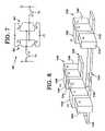
- FIG. 7is a schematic diagram of a conventional six-transistor SRAM cell.
- FIG. 8is a perspective view of the transistors P 2 , N 1 , and N 3 of the six-transistor SRAM cell illustrated in FIG. 7 , formed in accordance with the present invention.
- FIG. 9is a schematic diagram of a six-transistor SRAM cell formed in accordance with the present invention.
- FIGS. 10-26illustrate the process flow for forming a p-channel inverted FinFET transistor (P-IFinFET), fin underpass (UP), n-channel FinFET transistor (FinFET) and fin-based buried contact (BC) in accordance with the present invention.
- P-IFinFETp-channel inverted FinFET transistor
- UPfin underpass
- FinFETFinFET
- BCfin-based buried contact
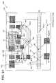
- FIG. 27depicts a layout of a SRAM cell produced in accordance with the present invention.
- the present inventionaddresses the above-mentioned problems, as well as others, by providing an inverted FinFET thin film transistor, and a static random access memory (SRAM) cell that is formed using inverted FinFET thin film transistors.
- SRAMstatic random access memory
- FIG. 1A cross-sectional view of a conventional FinFET thin film transistor 10 is illustrated in FIG. 1 .
- a plan view of the FinFET transistor 10is illustrated in FIG. 2 .
- the FinFET transistor 10is formed on an insulating layer 12 (e.g., a layer of SiO 2 ).
- the FinFET transistor 10comprises a fin 14 , typically formed of silicon or other suitable semiconductor material, and a gate 16 , formed of polysilicon or other suitable conductive material, running over the fin 14 .
- a channel 18is formed in the portion of the fin 14 that extends under the gate 16 .
- the source 20 and drain 22 of the FinFET transistor 10are located at opposing ends of the fin 14 .
- the benefits provided by such a FinFET transistor 10include, for example, smaller size, reduced power consumption, and faster switching times due to the “double gate” structure surrounding the channel 18 .
- FIG. 3A cross-sectional view of an inverted FinFET thin film transistor 30 in accordance with the present invention is illustrated in FIG. 3 .
- FIG. 4A plan view of the inverted FinFET transistor 30 is illustrated in FIG. 4 .
- a fin 32typically formed of silicon or other suitable semiconductor material, acts as the gate 34 of the transistor, rather than as the body, source and drain, as would be the case for a typical FinFET transistor (e.g., see FIGS. 1-2 ).
- a layer 36formed of polysilicon or other suitable semi-conductive material, crosses the fin 32 and forms the channel 38 , source 40 , and drain 42 of the inverted FinFET 30 transistor, rather than the gate, as would be the case for a typical FinFET transistor (e.g., see FIGS. 1-2 ).
- Other semiconductor and conductive materialsmay be used to form the fin 32 and layer 36 .
- FIG. 5A more detailed view of a p-channel inverted FinFET transistor 50 in accordance of the present invention is shown in FIG. 5 .
- the p-channel inverted FinFET transistor 50includes an n+ doped silicon fin 52 that acts as the gate 54 of the transistor 50 .
- the gate 54is covered by a layer 56 of a gate insulator (e.g., SiO 2 ).
- a layer 58 of polysiliconcrosses the fin 52 and forms the body region 60 of the transistor 50 .
- the body region 60includes a p+ doped source 62 , p+ doped drain 64 , and channel 72 of the transistor 50 .
- the channel 72includes lightly p doped areas on either side of the gate 54 and below spacers 68 , which are formed on the sides of the transistor 50 , and may comprise, for example, SiO 2 , Si 3 N 4 , etc.
- the p+ doped source 62 and drain 64 , and a p+ doped region 70 of the body region 60 located over the gate 54supply the channel 72 with p-type carriers.
- the p-channel inverted FinFET transistor 50the operation of which may be slightly degraded because of the polycrystalline silicon which comprises channel 72 , is useful as the pull-up device in a SRAM cell.
- the fin underpass 80has a structure similar to that of the p-channel inverted FinFET transistor 50 described above.
- the fin underpass 80includes an n+ doped silicon fin 82 that is covered by an insulating layer 84 of a gate insulator such as SiO 2 .
- the layer of polysilicon 86 running over the fin 82is n+ doped.
- the n+ doped polysilicon layer 86passes over, and is insulated from, the n+ doped fin 82 by the insulating layer 84 .
- FIG. 7A schematic diagram of a conventional six-transistor SRAM cell 90 is illustrated in FIG. 7 .
- the SRAM cell 90includes a pair of cross-coupled inverters 92 , 94 to store a data bit state, and a pair of n-channel coupling transistors N 1 , N 2 to read and write a data bit between the cross-coupled inverters 92 , 94 and the bitlines BL, BL (BAR).
- the inverter 92includes a p-channel pull-up transistor P 1 and a n-channel pull-down transistor N 3 .
- the inverter 94includes a p-channel pull-up transistor P 2 and a n-channel pull-down transistor N 4 .
- Such a SRAM cell 90is well known and will not be presented in detail.
- a six-transistor SRAM cellis produced, for example, using an industry standard 100 nm node (see, e.g., Brighten et al, “Integration of High Performance, Low Leakage and Mixed Signal Features into a 100 nm CMOS Technology,” 2002 Symposium on VLSI Technology, Digest of Technical papers P 62-3, June 2002), the resultant standard SRAM cell size is approximately 1.26 ⁇ m 2 .
- a SRAM cellcan be produced that is approximately 65% of the size of a standard SRAM cell produced using an industry standard 100 nm node.
- FIG. 8The formation of the transistors P 2 , N 1 , and N 3 ( FIG. 7 ), using a p-channel inverted FinFET transistor in accordance with the present invention, and two n-channel FinFET transistors, respectively, is illustrated in FIG. 8 .
- the process flow for forming the inverted FinFET transistor and FinFET transistor, as well as a fin underpass and a fin-based buried contact,will be presented in detail below.
- silicon fins 100 , 102are formed in the same process step on a substrate.
- the silicon fins 100 , 102may comprise separate fins, or may comprise different portions of the same fin.
- a layer 104 of polysiliconextends between, and passes over the sides and tops of, the fins 100 and 102 .
- a portion of the silicon fin 100is n+ doped to produce the gate 108 of P 2
- a portion of the layer 104 of polysiliconis p+ doped to form a body region including the source 110 , channel 112 , and drain 114 of P 2 .
- the channel 112 of P 2passes over the gate 108 .
- the source 110 and drain 114 of P 2are located on either side of the gate 108 and are connected by the channel 112 .
- the body region of the n-channel FinFET transistor N 3is formed using a lightly doped portion of the fin 102 .
- the gate 122 of N 3is formed using a n+ doped portion of the polysilicon layer 104 .
- the polysilicon layer 104is used to form the gate 122 of N 3 and the source 110 , channel 112 , and drain 114 of P 2 .
- the polysilicon layer 104connects the gate 122 of N 3 to the drain 114 of P 2 .
- a self-aligned metal silicide(not shown), such as CoSi 2 , can be used to bridge the n+ to p+ junction in the polysilicon layer 104 to ensure good electrical conductivity from gate 122 to drain 114 .
- the body region of the n-channel FinFET transistor N 1is formed using a lightly doped portion of the fin 100 .
- the gate 129 of N 1is formed using a n+ doped portion of the layer 106 of polysilicon.
- the fin 100is used to form the gate 108 of P 2 and the drain 124 , channel 126 , and source 128 of N 1 . Further, the fin 100 connects the gate 108 of P 2 to the drain 124 of N 1 .
- FIG. 9A six-transistor SRAM cell 130 formed in accordance with the present invention is illustrated in FIG. 9 .
- the SRAM cell 130operates in a convention manner.
- the SRAM cell 130is formed using two p-channel inverted FinFET transistors P 1 , P 2 , four n-channel FinFET transistors N 1 , N 2 , N 3 , and N 4 , two fin underpasses UP 1 , UP 2 , and five fin-based buried contacts BC 1 , BC 2 , BC 3 , BC 4 , and BC 5 .
- the underpass UP 1allows the conductive path between the drain of N 1 and BC 1 to insulatively pass under the conductive path between BC 3 and BC 5 .
- the underpass UP 2allows the conductive path between BC 5 and BC 2 to insulatively pass under the conductive path between BC 1 and BC 4 .
- the layout of the SRAM cell 130is simplified, and the size of the SRAM cell 130 is significantly reduced compared to a standard SRAM cell with similar minimum feature sizes produced using known techniques.
- the p-channel inverted FinFET transistor, n-channel FinFET transistor, fin underpass, and fin-based buried contactmay also be used individually or in other combinations in other semiconductor devices.
- the doping of these structuremay also vary.
- a n-channel inverted FinFET transistormay be formed by using p-type doping in place of n-type doping and vice-versa.
- a layer 142 of SiO 2 and a masking layer 144 of Si 3 N 4are formed on a silicon-on-insulator (SOI) wafer 140 .
- the SOI wafer 140comprises a silicon substrate 146 , a buried oxide (BOX) layer 148 , and a layer of silicon 150 approximately 30 nm to 170 nm thick.
- the Si 3 N 4 layeris patterned and etched to provide Si 3 N 4 shapes 152 that are approximately 5 nm to 30 nm wide.
- the SiO 2 layer 142is patterned and etched to form SiO 2 shapes 154 as shown in FIG. 11 .
- the SiO 2 layer 142is first etched using an anisotropic etch. This is followed by an isotropic oxide etch to adjust the final width of the SiO 2 shapes 154 .
- the SiO 2 shapes 154are used as a mask during an anisotropic etch of the silicon layer 150 .
- the etchingstops at the surface of the BOX layer 148 .
- the resultant silicon fins 156 A, 156 B, 156 C, and 156 Dhaving a width of approximately 1 nm to 30 nm, are used to form the fin portions of a p-channel inverted FinFET transistor (P-IFinFET), a fin underpass (UP), a n-channel FinFET transistor (FinFET) and a fin-based buried contact (BC).
- P-IFinFETp-channel inverted FinFET transistor
- UPfin underpass
- FinFETFinFET
- BCfin-based buried contact
- a layer 158 of sacrificial SiO 2is then grown on the sides of the silicon fins 156 A-D.
- the layer 158 of sacrificial SiO 2protects the silicon fins 156 A prior to, and during, a subsequent implantation step.
- a photoresist mask layer 160is then applied and patterned to selectively expose the fins 156 A, 156 B, and 156 D as illustrated in FIG. 13 .
- the fin 156 Cremains covered by the mask layer 160 .
- An n-type dopant 161such as phosphorus or arsenic, is then implanted via ion implantation into the exposed fins 156 A, 156 B, and 156 D.
- the fin 156 Cremains undoped because of the remaining mask layer 160 .
- the remaining mask layer 160 and the sacrificial SiO 2 layer 158are stripped away.
- a layer 164 of undoped polysiliconis then deposited to a thickness of approximately 10 nm to 75 nm. The thickness of the undoped polysilicon layer 164 is less than the combined thicknesses of the silicon layer 150 and the SiO 2 layer 142 ( FIG. 10 ).
- the spacer layer 166is then anisotropically etched to form sidewall spacers 168 on the undoped polysilicon layer 164 .
- the fins 156 A, 156 B, and 156 Dare n+ doped, while the fin 156 C is undoped.
- a photoresist mask layer 170is applied and patterned to selectively mask off the P-IFinFET region around the fin 156 A where the p-channel inverted FinFET transistor is to be formed.
- the exposed sidewall spacers 168 next to the fins 156 B, 156 C, and 156 Dare then isotropically etched away.
- all regions except for the BC regionare selectively masked off with a BC photoresist mask 172 .
- the polysilicon layer 164 in the exposed BC regionis then etched away and the exposed layer 162 of gate oxide on the sides of the fin 156 D is stripped away.
- a thin film 174 of undoped polysiliconis deposited as shown in FIG. 18 .
- the polysilicon layer 174is selectively etched back with a mask (not shown) selectively covering the other structures until the sidewall spacers 168 next to the fin 156 A are exposed.
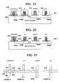
- FIG. 19The next step in the process is illustrated in FIG. 19 .
- a photoresist mask layer 176is deposited and patterned to cover the P-IFinFET, UP, FinFET and BC regions.
- the unmasked areas of the polysilicon layers 164 , 174are then etched away.
- the mask layer 176is then stripped away as shown in FIG. 20 .
- a top view corresponding to FIG. 20is provided in FIG. 21 .
- fins 156 A, 156 B, and 156 Dare all n+ doped
- fin 156 Cis undoped
- polysilicon layers 164 , 174are undoped.
- a n-implant photoresist mask layer 178is deposited and patterned to selectively cover the P-IFinFET region.
- An n-type dopant 180such as phosphorus or arsenic, is then implanted via ion implantation into the undoped polysilicon layers 164 , 174 , of the UP, FinFET and BC regions. After implantation, the mask layer 178 is stripped away.
- FIG. 23A top view corresponding to FIG. 22 is provided in FIG. 23 .
- fins 156 A, 156 B, and 156 Dare n+ doped
- fin 156 Cis lightly n doped
- the polysilicon layers 164 , 174 of the UP, FinFET and BC regionsare n+ doped
- the polysilicon layer 164 in the P-IFinFET regionremains undoped.
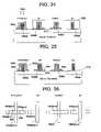
- a p-implant photoresist mask layer 182is then deposited and patterned to selectively cover the UP, FinFET and BC regions.
- a p-type dopant 184such as boron, is then implanted via ion implantation into the undoped polysilicon layer 164 of the P-IFinFET region. After implantation, the mask layer 182 is stripped away as shown in FIG. 25 .
- fins 156 A, 156 B, and 156 Dare n+ doped
- fin 156 Cis lightly n doped
- the polysilicon layers 164 , 174 in the UP, FinFET and BC regionsare n+ doped
- the polysilicon layer 164 in the P-IFinFET regionis p+ doped (lightly doped under the sidewall spacers 168 ).
- a light oxidation(approximately 1 nm to 6 nm thick) follows.
- a top view corresponding to FIG. 25is provided in FIG. 26 . Spacers, selective silicon, source/drain and gate contacts are then applied (not shown) as per conventional FinFET processing.
- FIG. 27depicts a layout 200 of an SRAM cell 130 (see, e.g., FIG. 9 ) produced in accordance with the present invention.
- the layout of the SRAM cell 130includes two p-channel inverted FinFET transistors P 1 , P 2 , four n-channel FinFET transistors N 1 , N 2 , N 3 , and N 4 , two fin underpasses UP 1 , UP 2 , and five fin-based buried contacts BC 1 , BC 2 , BC 3 , BC 4 , and BC 5 , each formed in accordance with the process flow detailed in FIGS. 10-26 .
- the silicon finse.g., fins 100 , 102 , FIG. 8 and fins 156 A-D, FIG.
- the layout 200 produced in accordance with the present inventionis simpler and more compact than a SRAM cell designed using known CMOS techniques.
- the inventionis useful for integrated circuit processing, and more particularly for producing an inverted FinFET thin film transistor, and for producing denser static random access memory (SRAM) using inverted FinFET thin film transistors.
- SRAMstatic random access memory
Landscapes
- Semiconductor Memories (AREA)
- Thin Film Transistor (AREA)
Abstract
Description
Claims (8)
Priority Applications (1)
| Application Number | Priority Date | Filing Date | Title |
|---|---|---|---|
| US10/539,335US7378710B2 (en) | 2002-12-19 | 2002-12-19 | FinFET SRAM cell using inverted FinFET thin film transistors |
Applications Claiming Priority (2)
| Application Number | Priority Date | Filing Date | Title |
|---|---|---|---|
| US10/539,335US7378710B2 (en) | 2002-12-19 | 2002-12-19 | FinFET SRAM cell using inverted FinFET thin film transistors |
| PCT/US2002/040868WO2004059703A1 (en) | 2002-12-19 | 2002-12-19 | Finfet sram cell using inverted finfet thin film transistors |
Publications (2)
| Publication Number | Publication Date |
|---|---|
| US20060068531A1 US20060068531A1 (en) | 2006-03-30 |
| US7378710B2true US7378710B2 (en) | 2008-05-27 |
Family
ID=36099743
Family Applications (1)
| Application Number | Title | Priority Date | Filing Date |
|---|---|---|---|
| US10/539,335Expired - Fee RelatedUS7378710B2 (en) | 2002-12-19 | 2002-12-19 | FinFET SRAM cell using inverted FinFET thin film transistors |
Country Status (1)
| Country | Link |
|---|---|
| US (1) | US7378710B2 (en) |
Cited By (8)
| Publication number | Priority date | Publication date | Assignee | Title |
|---|---|---|---|---|
| US20090020819A1 (en)* | 2007-07-16 | 2009-01-22 | Anderson Brent A | Fin-type field effect transistor structure with merged source/drain silicide and method of forming the structure |
| US20090101978A1 (en)* | 2007-10-17 | 2009-04-23 | Anderson Brent A | Fin-type field effect transistor structure with merged source/drain silicide and method of forming the structure |
| US20120074495A1 (en)* | 2010-09-24 | 2012-03-29 | Taiwan Semiconductor Manufacturing Company, Ltd. | Series FinFET Implementation Schemes |
| US20120202330A1 (en)* | 2005-12-02 | 2012-08-09 | Nec Corporation | Semiconductor device and method of manufacturing the same |
| US8956932B2 (en) | 2013-02-25 | 2015-02-17 | International Business Machines Corporation | U-shaped semiconductor structure |
| US9048120B2 (en) | 2012-11-26 | 2015-06-02 | Samsung Electronics Co., Ltd. | Integrated junction and junctionless nanotransistors |
| US9601497B1 (en)* | 2016-04-28 | 2017-03-21 | Taiwan Semiconductor Manufacturing Co., Ltd. | Static random access memory and method of manufacturing the same |
| DE102017120848A1 (en)* | 2017-08-31 | 2019-02-28 | Taiwan Semiconductor Manufacturing Co. Ltd. | Use of three or more masks to define contact line blocking components in FinFET SRAM fabrication |
Families Citing this family (24)
| Publication number | Priority date | Publication date | Assignee | Title |
|---|---|---|---|---|
| US7378710B2 (en)* | 2002-12-19 | 2008-05-27 | International Business Machines Corporation | FinFET SRAM cell using inverted FinFET thin film transistors |
| JP2006019578A (en)* | 2004-07-02 | 2006-01-19 | Toshiba Corp | Semiconductor device and manufacturing method thereof |
| US7754560B2 (en)* | 2006-01-10 | 2010-07-13 | Freescale Semiconductor, Inc. | Integrated circuit using FinFETs and having a static random access memory (SRAM) |
| US7723805B2 (en)* | 2006-01-10 | 2010-05-25 | Freescale Semiconductor, Inc. | Electronic device including a fin-type transistor structure and a process for forming the electronic device |
| US7709303B2 (en)* | 2006-01-10 | 2010-05-04 | Freescale Semiconductor, Inc. | Process for forming an electronic device including a fin-type structure |
| US7763534B2 (en) | 2007-10-26 | 2010-07-27 | Tela Innovations, Inc. | Methods, structures and designs for self-aligning local interconnects used in integrated circuits |
| US7956421B2 (en) | 2008-03-13 | 2011-06-07 | Tela Innovations, Inc. | Cross-coupled transistor layouts in restricted gate level layout architecture |
| US7446352B2 (en)* | 2006-03-09 | 2008-11-04 | Tela Innovations, Inc. | Dynamic array architecture |
| US8217435B2 (en) | 2006-12-22 | 2012-07-10 | Intel Corporation | Floating body memory cell having gates favoring different conductivity type regions |
| JP5035335B2 (en)* | 2007-03-20 | 2012-09-26 | 独立行政法人産業技術総合研究所 | SRAM device |
| US7710765B2 (en)* | 2007-09-27 | 2010-05-04 | Micron Technology, Inc. | Back gated SRAM cell |
| US8659088B2 (en) | 2008-03-28 | 2014-02-25 | National Institute Of Advanced Industrial Science And Technology | SRAM cell and SRAM device |
| KR100971411B1 (en)* | 2008-05-21 | 2010-07-21 | 주식회사 하이닉스반도체 | Method of forming vertical channel transistor in semiconductor device |
| US8399931B2 (en)* | 2010-06-30 | 2013-03-19 | Taiwan Semiconductor Manufacturing Company, Ltd. | Layout for multiple-fin SRAM cell |
| TWI476768B (en)* | 2011-10-21 | 2015-03-11 | Univ Nat Chiao Tung | A static random access memory (sram) cell |
| KR101823105B1 (en)* | 2012-03-19 | 2018-01-30 | 삼성전자주식회사 | Method for fabricating field effect transistor |
| US9583398B2 (en)* | 2012-06-29 | 2017-02-28 | Taiwan Semiconductor Manufacturing Company, Ltd. | Integrated circuit having FinFETS with different fin profiles |
| US9117842B2 (en) | 2013-03-13 | 2015-08-25 | Globalfoundries Inc. | Methods of forming contacts to source/drain regions of FinFET devices |
| US20140273365A1 (en)* | 2013-03-13 | 2014-09-18 | Globalfoundries Inc. | Methods of forming contacts to source/drain regions of finfet devices by forming a region that includes a schottky barrier lowering material |
| CN104124210B (en)* | 2013-04-28 | 2016-12-28 | 中芯国际集成电路制造(上海)有限公司 | The forming method of semiconductor structure |
| US9984191B2 (en)* | 2014-08-29 | 2018-05-29 | Taiwan Semiconductor Manufacturing Company | Cell layout and structure |
| US9680018B2 (en)* | 2015-09-21 | 2017-06-13 | International Business Machines Corporation | Method of forming high-germanium content silicon germanium alloy fins on insulator |
| US10074657B2 (en)* | 2016-04-28 | 2018-09-11 | Taiwan Semiconductor Manufacturing Company, Ltd. | Method of manufacturing fins and semiconductor device which includes fins |
| WO2018182609A1 (en)* | 2017-03-30 | 2018-10-04 | Intel Corporation | Vertical multi-gate thin film transistors |
Citations (8)
| Publication number | Priority date | Publication date | Assignee | Title |
|---|---|---|---|---|
| US6300182B1 (en)* | 2000-12-11 | 2001-10-09 | Advanced Micro Devices, Inc. | Field effect transistor having dual gates with asymmetrical doping for reduced threshold voltage |
| US6413802B1 (en)* | 2000-10-23 | 2002-07-02 | The Regents Of The University Of California | Finfet transistor structures having a double gate channel extending vertically from a substrate and methods of manufacture |
| US6475890B1 (en)* | 2001-02-12 | 2002-11-05 | Advanced Micro Devices, Inc. | Fabrication of a field effect transistor with an upside down T-shaped semiconductor pillar in SOI technology |
| US6525403B2 (en)* | 2000-09-28 | 2003-02-25 | Kabushiki Kaisha Toshiba | Semiconductor device having MIS field effect transistors or three-dimensional structure |
| US20050156202A1 (en)* | 2004-01-17 | 2005-07-21 | Hwa-Sung Rhee | At least penta-sided-channel type of FinFET transistor |
| US20060011977A1 (en)* | 2004-07-02 | 2006-01-19 | Kabushiki Kaisha Toshiba | Semiconductor device and method of fabricating the same |
| US20060068531A1 (en)* | 2002-12-19 | 2006-03-30 | Matthew Breitwisch | Finfet sram cell using inverted finfet thin film transistors |
| US20070047357A1 (en)* | 2005-08-18 | 2007-03-01 | Samsung Electronics Co., Ltd. | Semiconductor memory device |
- 2002
- 2002-12-19USUS10/539,335patent/US7378710B2/ennot_activeExpired - Fee Related
Patent Citations (9)
| Publication number | Priority date | Publication date | Assignee | Title |
|---|---|---|---|---|
| US6525403B2 (en)* | 2000-09-28 | 2003-02-25 | Kabushiki Kaisha Toshiba | Semiconductor device having MIS field effect transistors or three-dimensional structure |
| US6413802B1 (en)* | 2000-10-23 | 2002-07-02 | The Regents Of The University Of California | Finfet transistor structures having a double gate channel extending vertically from a substrate and methods of manufacture |
| US6300182B1 (en)* | 2000-12-11 | 2001-10-09 | Advanced Micro Devices, Inc. | Field effect transistor having dual gates with asymmetrical doping for reduced threshold voltage |
| US6475890B1 (en)* | 2001-02-12 | 2002-11-05 | Advanced Micro Devices, Inc. | Fabrication of a field effect transistor with an upside down T-shaped semiconductor pillar in SOI technology |
| US20060068531A1 (en)* | 2002-12-19 | 2006-03-30 | Matthew Breitwisch | Finfet sram cell using inverted finfet thin film transistors |
| US20050156202A1 (en)* | 2004-01-17 | 2005-07-21 | Hwa-Sung Rhee | At least penta-sided-channel type of FinFET transistor |
| US20060011977A1 (en)* | 2004-07-02 | 2006-01-19 | Kabushiki Kaisha Toshiba | Semiconductor device and method of fabricating the same |
| US7221032B2 (en)* | 2004-07-02 | 2007-05-22 | Kabushiki Kaisha Toshiba | Semiconductor device including FinFET having vertical double gate structure and method of fabricating the same |
| US20070047357A1 (en)* | 2005-08-18 | 2007-03-01 | Samsung Electronics Co., Ltd. | Semiconductor memory device |
Cited By (20)
| Publication number | Priority date | Publication date | Assignee | Title |
|---|---|---|---|---|
| US20120202330A1 (en)* | 2005-12-02 | 2012-08-09 | Nec Corporation | Semiconductor device and method of manufacturing the same |
| US7692254B2 (en)* | 2007-07-16 | 2010-04-06 | International Business Machines Corporation | Fin-type field effect transistor structure with merged source/drain silicide and method of forming the structure |
| US20090020819A1 (en)* | 2007-07-16 | 2009-01-22 | Anderson Brent A | Fin-type field effect transistor structure with merged source/drain silicide and method of forming the structure |
| US20090101978A1 (en)* | 2007-10-17 | 2009-04-23 | Anderson Brent A | Fin-type field effect transistor structure with merged source/drain silicide and method of forming the structure |
| US7851865B2 (en) | 2007-10-17 | 2010-12-14 | International Business Machines Corporation | Fin-type field effect transistor structure with merged source/drain silicide and method of forming the structure |
| US20120074495A1 (en)* | 2010-09-24 | 2012-03-29 | Taiwan Semiconductor Manufacturing Company, Ltd. | Series FinFET Implementation Schemes |
| US8659072B2 (en)* | 2010-09-24 | 2014-02-25 | Taiwan Semiconductor Manufacturing Company, Ltd. | Series FinFET implementation schemes |
| US9171845B2 (en) | 2012-11-26 | 2015-10-27 | Samsung Electronics Co., Ltd. | Integrated junction and junctionless nanotransistors |
| US9048120B2 (en) | 2012-11-26 | 2015-06-02 | Samsung Electronics Co., Ltd. | Integrated junction and junctionless nanotransistors |
| US9202893B2 (en) | 2013-02-25 | 2015-12-01 | Globalfoundries Inc | U-shaped semiconductor structure |
| US8956932B2 (en) | 2013-02-25 | 2015-02-17 | International Business Machines Corporation | U-shaped semiconductor structure |
| US9318580B2 (en) | 2013-02-25 | 2016-04-19 | Globalfoundries Inc. | U-shaped semiconductor structure |
| US9601497B1 (en)* | 2016-04-28 | 2017-03-21 | Taiwan Semiconductor Manufacturing Co., Ltd. | Static random access memory and method of manufacturing the same |
| US10083969B2 (en) | 2016-04-28 | 2018-09-25 | Taiwan Semiconductor Manufacturing Co., Ltd. | Static random access memory and method of manufacturing the same |
| DE102017120848A1 (en)* | 2017-08-31 | 2019-02-28 | Taiwan Semiconductor Manufacturing Co. Ltd. | Use of three or more masks to define contact line blocking components in FinFET SRAM fabrication |
| US10411020B2 (en) | 2017-08-31 | 2019-09-10 | Taiwan Semiconductor Manufacturing Co., Ltd. | Using three or more masks to define contact-line-blocking components in FinFET SRAM fabrication |
| US10453852B2 (en) | 2017-08-31 | 2019-10-22 | Taiwan Semiconductor Manufacturing Co., Ltd. | Using three or more masks to define contact-line-blocking components in FinFET SRAM fabrication |
| US10535668B1 (en) | 2017-08-31 | 2020-01-14 | Taiwan Semiconductor Manufacturing Co., Ltd. | Using three or more masks to define contact-line-blocking components in FinFET SRAM fabrication |
| US10714488B2 (en) | 2017-08-31 | 2020-07-14 | Taiwan Semiconductor Manufacturing Co., Ltd. | Using three or more masks to define contact-line-blocking components in FinFET SRAM fabrication |
| DE102017120848B4 (en) | 2017-08-31 | 2023-07-06 | Taiwan Semiconductor Manufacturing Co. Ltd. | Use of three or more masks to define contact line blocking components in FinFET SRAM fabrication |
Also Published As
| Publication number | Publication date |
|---|---|
| US20060068531A1 (en) | 2006-03-30 |
Similar Documents
| Publication | Publication Date | Title |
|---|---|---|
| US7378710B2 (en) | FinFET SRAM cell using inverted FinFET thin film transistors | |
| KR100530305B1 (en) | Vertical mosfet sram cell | |
| US9048122B2 (en) | FinFET drive strength modification | |
| US6664582B2 (en) | Fin memory cell and method of fabrication | |
| US8053841B2 (en) | Semiconductor device having a fin transistor | |
| US7737501B2 (en) | FinFET SRAM with asymmetric gate and method of manufacture thereof | |
| KR101275758B1 (en) | Semiconductor device including a plurality of stacked transistors and method of fabricating the same | |
| US7888201B2 (en) | Semiconductor-on-insulator SRAM configured using partially-depleted and fully-depleted transistors | |
| US7915691B2 (en) | High density SRAM cell with hybrid devices | |
| US6774437B2 (en) | Fin-based double poly dynamic threshold CMOS FET with spacer gate and method of fabrication | |
| US20050023633A1 (en) | Semiconductor-on-insulator SRAM configured using partially-depleted and fully-depleted transistors | |
| EP1586108B1 (en) | Finfet sram cell using inverted finfet thin film transistors | |
| JPH11317459A (en) | Method for fabricating dual gate oxide dual work function CMOS | |
| KR20050094576A (en) | Three dimensional cmos field effect transistor and method of fabricating the same | |
| CN103579242B (en) | There is SRAM integrated circuit and the manufacture method thereof burying saddle type fin field-effect transistor | |
| US5426315A (en) | Thin-film transistor having an inlaid thin-film channel region | |
| US20060281302A1 (en) | Semiconductor damascene trench and methods thereof | |
| US20190172822A1 (en) | Logic layout with reduced area and method of making the same | |
| KR100654535B1 (en) | FinFET Static Memory Cell Using Reverse FIFNFC Thin Film Transistor | |
| TWI892505B (en) | Metal-oxide-semiconductor transistor and complementary metal-oxide-semiconductor circuit related | |
| KR100318318B1 (en) | Manufacturing Method for Cell of Semiconductor Memory Device | |
| WO2007063988A1 (en) | Semiconductor device and method for manufacturing same | |
| KR0138320B1 (en) | Thin film transistor and their manufacture | |
| KR960010073B1 (en) | Semiconductor device and the manufacturing method thereof | |
| KR20050082048A (en) | Dram and method of manufacturing for the same |
Legal Events
| Date | Code | Title | Description |
|---|---|---|---|
| AS | Assignment | Owner name:INTERNATIONAL BUSINESS MACHINES CORPORATION, NEW Y Free format text:ASSIGNMENT OF ASSIGNORS INTEREST;ASSIGNORS:BREITWISCH, MATTHEW;NOWAK, EDWARD J.;REEL/FRAME:013640/0450 Effective date:20021216 | |
| AS | Assignment | Owner name:INTERNATIONAL BUSINESS MACHINES CORPORATION, NEW Y Free format text:ASSIGNMENT OF ASSIGNORS INTEREST;ASSIGNORS:BREITWISCH, MATTHEW;NOWAK, EDWARD J.;REEL/FRAME:016517/0640 Effective date:20050613 | |
| STCF | Information on status: patent grant | Free format text:PATENTED CASE | |
| FEPP | Fee payment procedure | Free format text:PAYOR NUMBER ASSIGNED (ORIGINAL EVENT CODE: ASPN); ENTITY STATUS OF PATENT OWNER: LARGE ENTITY | |
| FPAY | Fee payment | Year of fee payment:4 | |
| AS | Assignment | Owner name:GLOBALFOUNDRIES U.S. 2 LLC, NEW YORK Free format text:ASSIGNMENT OF ASSIGNORS INTEREST;ASSIGNOR:INTERNATIONAL BUSINESS MACHINES CORPORATION;REEL/FRAME:036550/0001 Effective date:20150629 | |
| AS | Assignment | Owner name:GLOBALFOUNDRIES INC., CAYMAN ISLANDS Free format text:ASSIGNMENT OF ASSIGNORS INTEREST;ASSIGNORS:GLOBALFOUNDRIES U.S. 2 LLC;GLOBALFOUNDRIES U.S. INC.;REEL/FRAME:036779/0001 Effective date:20150910 | |
| FPAY | Fee payment | Year of fee payment:8 | |
| AS | Assignment | Owner name:ALSEPHINA INNOVATIONS INC., CANADA Free format text:ASSIGNMENT OF ASSIGNORS INTEREST;ASSIGNOR:GLOBALFOUNDRIES INC.;REEL/FRAME:049709/0871 Effective date:20181126 | |
| FEPP | Fee payment procedure | Free format text:MAINTENANCE FEE REMINDER MAILED (ORIGINAL EVENT CODE: REM.); ENTITY STATUS OF PATENT OWNER: LARGE ENTITY | |
| LAPS | Lapse for failure to pay maintenance fees | Free format text:PATENT EXPIRED FOR FAILURE TO PAY MAINTENANCE FEES (ORIGINAL EVENT CODE: EXP.); ENTITY STATUS OF PATENT OWNER: LARGE ENTITY | |
| STCH | Information on status: patent discontinuation | Free format text:PATENT EXPIRED DUE TO NONPAYMENT OF MAINTENANCE FEES UNDER 37 CFR 1.362 | |
| AS | Assignment | Owner name:TAIWAN SEMICONDUCTOR MANUFACTURING COMPANY, LTD., TAIWAN Free format text:ASSIGNMENT OF ASSIGNORS INTEREST;ASSIGNOR:ALSEPHINA INNOVATIONS, INC.;REEL/FRAME:053351/0839 Effective date:20200211 | |
| FP | Lapsed due to failure to pay maintenance fee | Effective date:20200527 | |
| AS | Assignment | Owner name:GLOBALFOUNDRIES INC., CAYMAN ISLANDS Free format text:RELEASE BY SECURED PARTY;ASSIGNOR:WILMINGTON TRUST, NATIONAL ASSOCIATION;REEL/FRAME:054636/0001 Effective date:20201117 |