US7372886B2 - High thermal conductivity vertical cavity surface emitting laser (VCSEL) - Google Patents
High thermal conductivity vertical cavity surface emitting laser (VCSEL)Download PDFInfo
- Publication number
- US7372886B2 US7372886B2US10/862,753US86275304AUS7372886B2US 7372886 B2US7372886 B2US 7372886B2US 86275304 AUS86275304 AUS 86275304AUS 7372886 B2US7372886 B2US 7372886B2
- Authority
- US
- United States
- Prior art keywords
- layer
- vcsel
- htc
- reflector
- light generation
- Prior art date
- Legal status (The legal status is an assumption and is not a legal conclusion. Google has not performed a legal analysis and makes no representation as to the accuracy of the status listed.)
- Expired - Lifetime, expires
Links
- 230000003287optical effectEffects0.000claimsdescription19
- JBRZTFJDHDCESZ-UHFFFAOYSA-NAsGaChemical compound[As]#[Ga]JBRZTFJDHDCESZ-UHFFFAOYSA-N0.000claimsdescription11
- 229910001218Gallium arsenideInorganic materials0.000claimsdescription11
- 230000007480spreadingEffects0.000claimsdescription5
- 238000003892spreadingMethods0.000claimsdescription5
- MDPILPRLPQYEEN-UHFFFAOYSA-Naluminium arsenideChemical compound[As]#[Al]MDPILPRLPQYEEN-UHFFFAOYSA-N0.000claimsdescription2
- 229910052738indiumInorganic materials0.000claims1
- APFVFJFRJDLVQX-UHFFFAOYSA-Nindium atomChemical compound[In]APFVFJFRJDLVQX-UHFFFAOYSA-N0.000claims1
- 239000000203mixtureSubstances0.000description26
- 239000000463materialSubstances0.000description18
- 238000009826distributionMethods0.000description12
- 239000002019doping agentSubstances0.000description12
- 229910000980Aluminium gallium arsenideInorganic materials0.000description11
- 239000000758substrateSubstances0.000description11
- 230000008901benefitEffects0.000description7
- 229910052782aluminiumInorganic materials0.000description5
- XAGFODPZIPBFFR-UHFFFAOYSA-NaluminiumChemical compound[Al]XAGFODPZIPBFFR-UHFFFAOYSA-N0.000description5
- 230000000694effectsEffects0.000description5
- 239000004065semiconductorSubstances0.000description5
- 230000007704transitionEffects0.000description5
- GYHNNYVSQQEPJS-UHFFFAOYSA-NGalliumChemical compound[Ga]GYHNNYVSQQEPJS-UHFFFAOYSA-N0.000description4
- 229910000530Gallium indium arsenideInorganic materials0.000description4
- 238000013461designMethods0.000description4
- 229910052733galliumInorganic materials0.000description4
- 230000002411adverseEffects0.000description3
- 230000017525heat dissipationEffects0.000description3
- 230000020169heat generationEffects0.000description3
- 238000000034methodMethods0.000description3
- 238000002310reflectometryMethods0.000description3
- 125000006850spacer groupChemical group0.000description3
- 230000004888barrier functionEffects0.000description2
- 238000004891communicationMethods0.000description2
- 238000012986modificationMethods0.000description2
- 230000004048modificationEffects0.000description2
- 230000003071parasitic effectEffects0.000description2
- 230000008569processEffects0.000description2
- 229910052710siliconInorganic materials0.000description2
- 239000010703siliconSubstances0.000description2
- OKTJSMMVPCPJKN-UHFFFAOYSA-NCarbonChemical compound[C]OKTJSMMVPCPJKN-UHFFFAOYSA-N0.000description1
- -1InGaPInorganic materials0.000description1
- KXNLCSXBJCPWGL-UHFFFAOYSA-N[Ga].[As].[In]Chemical compound[Ga].[As].[In]KXNLCSXBJCPWGL-UHFFFAOYSA-N0.000description1
- 238000010521absorption reactionMethods0.000description1
- 229910045601alloyInorganic materials0.000description1
- 239000000956alloySubstances0.000description1
- AUCDRFABNLOFRE-UHFFFAOYSA-Nalumane;indiumChemical compound[AlH3].[In]AUCDRFABNLOFRE-UHFFFAOYSA-N0.000description1
- FTWRSWRBSVXQPI-UHFFFAOYSA-Nalumanylidynearsane;gallanylidynearsaneChemical compound[As]#[Al].[As]#[Ga]FTWRSWRBSVXQPI-UHFFFAOYSA-N0.000description1
- 238000013459approachMethods0.000description1
- 239000013590bulk materialSubstances0.000description1
- 229910052799carbonInorganic materials0.000description1
- 230000008859changeEffects0.000description1
- 238000013500data storageMethods0.000description1
- 230000003090exacerbative effectEffects0.000description1
- 229910052732germaniumInorganic materials0.000description1
- 238000003780insertionMethods0.000description1
- 230000037431insertionEffects0.000description1
- 238000004519manufacturing processMethods0.000description1
- 229910052751metalInorganic materials0.000description1
- 239000002184metalSubstances0.000description1
- 238000013021overheatingMethods0.000description1
- 239000002245particleSubstances0.000description1
- 238000012545processingMethods0.000description1
- 230000009467reductionEffects0.000description1
Images


Classifications
- H—ELECTRICITY
- H01—ELECTRIC ELEMENTS
- H01S—DEVICES USING THE PROCESS OF LIGHT AMPLIFICATION BY STIMULATED EMISSION OF RADIATION [LASER] TO AMPLIFY OR GENERATE LIGHT; DEVICES USING STIMULATED EMISSION OF ELECTROMAGNETIC RADIATION IN WAVE RANGES OTHER THAN OPTICAL
- H01S5/00—Semiconductor lasers
- H01S5/02—Structural details or components not essential to laser action
- H01S5/024—Arrangements for thermal management
- H01S5/02461—Structure or details of the laser chip to manipulate the heat flow, e.g. passive layers in the chip with a low heat conductivity
- H—ELECTRICITY
- H01—ELECTRIC ELEMENTS
- H01S—DEVICES USING THE PROCESS OF LIGHT AMPLIFICATION BY STIMULATED EMISSION OF RADIATION [LASER] TO AMPLIFY OR GENERATE LIGHT; DEVICES USING STIMULATED EMISSION OF ELECTROMAGNETIC RADIATION IN WAVE RANGES OTHER THAN OPTICAL
- H01S5/00—Semiconductor lasers
- H01S5/10—Construction or shape of the optical resonator, e.g. extended or external cavity, coupled cavities, bent-guide, varying width, thickness or composition of the active region
- H01S5/18—Surface-emitting [SE] lasers, e.g. having both horizontal and vertical cavities
- H01S5/183—Surface-emitting [SE] lasers, e.g. having both horizontal and vertical cavities having only vertical cavities, e.g. vertical cavity surface-emitting lasers [VCSEL]
- H01S5/18308—Surface-emitting [SE] lasers, e.g. having both horizontal and vertical cavities having only vertical cavities, e.g. vertical cavity surface-emitting lasers [VCSEL] having a special structure for lateral current or light confinement
- H01S5/18322—Position of the structure
- H01S5/18327—Structure being part of a DBR
- H—ELECTRICITY
- H01—ELECTRIC ELEMENTS
- H01S—DEVICES USING THE PROCESS OF LIGHT AMPLIFICATION BY STIMULATED EMISSION OF RADIATION [LASER] TO AMPLIFY OR GENERATE LIGHT; DEVICES USING STIMULATED EMISSION OF ELECTROMAGNETIC RADIATION IN WAVE RANGES OTHER THAN OPTICAL
- H01S5/00—Semiconductor lasers
- H01S5/04—Processes or apparatus for excitation, e.g. pumping, e.g. by electron beams
- H01S5/042—Electrical excitation ; Circuits therefor
- H01S5/0421—Electrical excitation ; Circuits therefor characterised by the semiconducting contacting layers
- H—ELECTRICITY
- H01—ELECTRIC ELEMENTS
- H01S—DEVICES USING THE PROCESS OF LIGHT AMPLIFICATION BY STIMULATED EMISSION OF RADIATION [LASER] TO AMPLIFY OR GENERATE LIGHT; DEVICES USING STIMULATED EMISSION OF ELECTROMAGNETIC RADIATION IN WAVE RANGES OTHER THAN OPTICAL
- H01S5/00—Semiconductor lasers
- H01S5/10—Construction or shape of the optical resonator, e.g. extended or external cavity, coupled cavities, bent-guide, varying width, thickness or composition of the active region
- H01S5/18—Surface-emitting [SE] lasers, e.g. having both horizontal and vertical cavities
- H01S5/183—Surface-emitting [SE] lasers, e.g. having both horizontal and vertical cavities having only vertical cavities, e.g. vertical cavity surface-emitting lasers [VCSEL]
- H01S5/18308—Surface-emitting [SE] lasers, e.g. having both horizontal and vertical cavities having only vertical cavities, e.g. vertical cavity surface-emitting lasers [VCSEL] having a special structure for lateral current or light confinement
Definitions
- the present inventionrelates to lasers, and more particularly, to an improved Vertical Cavity Surface-Emitting Laser.
- FIG. 1illustrates a cutaway side view of a sample prior art VCSEL 10 .
- the sample VCSEL 10is a conventional oxide-confined top emitting VCSEL 10 .
- the VCSEL 10includes a top reflector 20 and a bottom reflector 30 sandwiching an active region 40 .
- the reflectors 20 and 30 and the active region 40are fabricated on a substrate 50 .
- a bottom electrode 52is connected to the substrate while a top electrode 54 is connected to the top reflector 20 .
- the substrate 50may be n-type gallium arsenide (GaAs) doped with silicon.
- the bottom electrode 52forms an ohmic contact to the substrate 50 and is typically made of electrically conductive metal such as Gold-Germanium(AuGe) alloy.
- the active region 40includes a light generation layer 42 which is typically constructed from one or more quantum wells of InGaAs (indium gallium arsenide), GaAs (gallium arsenide), AlGaAs (aluminum gallium arsenide), or InAlGaAs (indium aluminum gallium arsenide).
- the light generation layer 42is separated from the top reflector 20 by a top spacer 44 and separated from the bottom reflector 30 by a bottom spacer 46 .
- the light generation layer 42is configured to generate light having a predetermined or known wavelength.
- the predetermined wavelengthcan vary widely, for example, within a range from approximately 650 nanometers (nm) to approximately 1,400 nanometers.
- the spacer layers 44 and 46may be fabricated using, for example, AlGaAs.
- the active region 40is sandwiched between the top reflector 20 and the bottom reflector 30 .
- the top reflector 20 and the bottom reflector 30are distributed Bragg reflectors (DBR) including alternating quarter wavelength thick layers of materials having differing optical index of refraction such as, for example, AlAs, GaAs, or AlGaAs having differing ratios of Aluminum and Gallium.
- DBRdistributed Bragg reflectors
- the top and bottom reflectors 20 and 30are also referred to as DBR mirrors 20 and 30 .
- each layer of the DBR mirrors 20 and 30has a thickness that is one-fourth ( 1 / 4 ) wavelength of the light generated by the active region 40 .
- a thicknessthat is one-fourth ( 1 / 4 ) wavelength of the light generated by the active region 40 .
- only eight layers (four pairs of layers)are illustrated in FIG. 1 for each of the DBR mirrors 20 and 30 .
- each of the DBR mirrors 20 and 30may include many more layers such as twenty or thirty pairs of layers.
- the active region 40is composed of a p-n junction and electrical current is injected into it.
- the DBR mirrors 20 and 30are doped with carefully designed profiles of n- or p-type dopants in order to both improve the bulk material conductivity and to minimize the voltage drop across the many heterobarriers formed at the interfaces between the alternating quarter-wave layers.
- one DBR mirroris doped n-type and the other doped p-type, forming the p-n junction and its associated heat dissipation in the active region 40 .
- the top DBR mirror 20may include p-doped GaAs, AlAs, or AlGaAs layers while the bottom DBR mirror 30 include n-doped GaAs, AlAs, or AlGaAs layers.
- the n dopantmay be silicon and the p dopant may be carbon.
- the layers of the top reflector 20are doped as p-type semiconductors and the layers of the bottom reflector 30 are doped as n-type semiconductors.
- the substrate 50is doped to create an n-type contact.
- the VCSEL 10 of such structure and its operationsare known in the art.
- electric currentis introduced to the VCSEL 10 via the electrodes 52 and 54 .
- photonslight particles
- optical gainis created that coherently amplifies the light which reflects back and forth between the DBR mirrors 20 and 30 .
- a portion of the lightis transmitted through the DBR mirrors 20 and 30 , and an opening 56 in the top electrical contact is typically employed to allow the transmitted light out of the device 10 . This escaping light is indicated by arrow 58 .
- Current confinement barrier 60is often used to direct the electrical current generally toward the middle of the active region 40 .
- the current confinement barrier 60insulates all but a circular or polygon-shaped area (from a top perspective, not shown) having a diameter that is typically similar to or smaller than the contact opening width 57 . Because most of the electrical current is directed toward a portion 43 of the light generation layer 42 , most of the light is generated within this portion 43 referred to as the active portion 43 herein.
- Excess heat in a VCSELhas a number of adverse effects including wavelength shift, gain reduction, increased absorption, refractive index shift and associated optical loss and DBR mirror reflectivity changes, leakage current, thermal lensing, and reduced efficiency. Combination of these effects and their spatial variation ultimately limits the maximum power, maximum single-lateral-mode power, maximum modulation bandwidth, and maximum efficiency the VCSEL 10 can achieve. Further, all of these parameters are of commercial importance.
- VCSELslong-wavelength (1300 nm wavelength of emitted light) could be commercially lucrative as light sources in optical communication links running at very high bit rates over metro-area link lengths of 10 kilometers (km) or more, but heat generation in the VCSELs makes it very challenging to simultaneously meet the modulation speed, optical power, and single-mode optical power requirements of such links.
- FIG. 2illustrates a lateral temperature distribution curve 70 along the active region 40 similar to results obtained by detailed finite element modeling.
- layer interval 42 irepresents and corresponds to the extent of the light generation layer 42 of the VCSEL 10 of FIG. 1
- active interval 43 irepresents and corresponds to the extent of the active portion 43 of the light generation layer 42 where most of the photons are generated.
- temperatureis highest at the active interval 43 i and the temperature drops off sharply at the edges of the active interval 43 i .
- Temperature differential 72 between the temperature at the active interval 43 i and the temperature outside the active interval 43 iis relatively large.
- the lateral temperature distribution curve 70suggests that heat is effectively trapped within the active portion 43 of the VCSEL 10 and is not effectively distributed or dissipated thereby exacerbating the heat problems of the VCSEL 10 of FIG. 1 .
- the heatis trapped within active portion 43 largely because of the normally conflicting requirements of high optical contrast, high electrical conductivity, and high thermal conductivity of the DBR mirrors 20 and 30 .
- DBR mirrorsare typically designed for high optical contrast and low electrical loss. Further, DBR mirrors normally have relatively poor thermal conductivity resulting in heat generated in active portion 43 being trapped and forming high peak temperatures as illustrated in curve 70 of FIG. 2 .
- the high peak temperaturenot only exacerbates problems associated with overheating such as limited efficiency, but the narrow spatial distribution caused by the heat confinement exacerbates problems associated with the lateral heat distribution such as thermal lensing.
- a light generating deviceincludes a light generation layer, a top reflector, a bottom reflector, and at least one high thermal conductivity (HTC) layer between.
- the HTC layercan be placed between the light generation layer and the bottom reflector, between the light generation layer and the top reflector, or both.
- the light generation layeris adapted to generate light having a first wavelength. Heat produced at the light generation layer is more efficiently dissipated due to the presence of the HTC layer.
- a light generating devicein another embodiment, includes a light generation layer, a top reflector, and a high thermal conductivity (HTC) bottom reflector.
- the light generation layeris adapted to generate light having a known wavelength. Heat produced at the light generation layer is more efficiently dissipated due to the fact that the bottom reflector is a HTC reflector.
- FIG. 1illustrates a cutaway side view of a sample VCSEL of prior art
- FIG. 2illustrates a lateral temperature distribution curve along a portion of the VCSEL of FIG. 1 ;
- FIG. 3illustrates a thermal resistivity curve representing approximate thermal resistivity of varying compositions of Al x Ga (1-x) As;
- FIG. 4illustrates one embodiment of a light generating device of the present invention
- FIG. 5illustrates a lateral temperature distribution curve along a portion of the VCSEL 100 of FIG. 4 ;
- FIGS. 6 , 7 A, 7 B, and 8 Aillustrate other embodiments of light generating device of the present invention.
- FIGS. 8B and 8Cillustrate alternative embodiments of a portion of light generation device of FIG. 8A .
- FIGS. 1 through 8Cillustrate various embodiments of the present invention.
- some sizes of structures or portionsmay be exaggerated relative to sizes of other structures or portions for illustrative purposes and, thus, are provided to illustrate the general structures of the present invention.
- various aspects of the present inventionare described with reference to a structure or a portion positioned “above” or “over” relative to other structures, portions, or both.
- relative terms and phrasessuch as “above” or “over” are used herein to describe one structure's or portion's relationship to another structure or portion as illustrated in the Figures.
- a light generating devicehaving a light generation layer adapted to generate light having a known wavelength, a top reflector above the light generation layer, a bottom reflector below the light generation layer, and at least one high thermal conductivity (HTC) layer between.
- the HTC layercan be placed between the light generation layer and the bottom reflector, between the light generation layer and the top reflector, or both. Heat produced at the light generation layer is more efficiently dissipated due to the presence of the HTC layer.
- the HTC layeris made of material having relatively high thermal conductivity compared to the top and the bottom reflectors. With this design, the heat generated at the light generation layer is removed and dissipated more efficiently.
- the present inventionis based on, in part, the realization that placement of material having high thermal conductivity near the light generation layer would aid in heat dissipation.
- material having high thermal conductivity near the light generation layerwould aid in heat dissipation.
- such materialneeds to meet a number of other requirements such as high optical transparency, an acceptable level of electrical conductivity, and ease of fabrication using known processes.
- the top and bottom reflectors 20 and 30are typically constructed using pairs of layers, each pair having a first layer of a first composition of Al x Ga (1-x) As and a second layer of a second composition of Al x Ga (1-x) As.
- the first layer and the second layerhave indices of refraction different from each other.
- the thickness of each layeris one quarter of the wavelength of the generated light.
- the layers, together,form Bragg reflectors.
- the layersare typically constructed from paired layers of AlAs, GaAs, or varying compositions of AlGaAs.
- the varying compositions of AlGaAsis often expressed in the following relationship: Al x Ga (1-x) As where X is a composition ratio of Aluminum and Gallium. For example, when X is zero, there is no Aluminum in the composition and the composition reduces to GaAs. When X is one (1), there is no Gallium in the composition, and the composition reduces to AlAs. When X is 0.3, for example, then the composition can be expressed as Al (0.3) Ga (0.7) As.
- the pairing of the layersis illustrated using a single pair 32 of layers within the bottom reflector 30 .
- the pair 32 of layersincludes a first layer 31 Al (0.2) Ga (0.8) (having a composition ratio of 0.2) and a second layer 33 Al (0.9) Ga (0.1) (having the composition ratio of 0.9).
- FIG. 3illustrates a thermal resistivity curve 80 representing approximate thermal resistivity of varying compositions of Al x Ga (1-x) As. Thermal resistivity is inverse of thermal conductivity.
- horizontal axis (x-axis)represents the composition ratio of Aluminum (X) and vertical axis (y-axis) represents the thermal resistivity in centimeter-degrees Kelvin per Watt (cm*K/W).
- cm*K/Wcentimeter-degrees Kelvin per Watt
- the first layer 31 Al (0.2) Ga (0.8) Ashas an approximate thermal resistivity of a little over 6.0 cm K/W as indicated by reference numeral 31 r .
- the second layer 33 Al (0.9) Ga (0.1) Ashas an approximate thermal resistivity of a 4.0 cm K/W as indicated by reference numeral 33 r.
- thermal resistivity curve 80for composition Al x Ga (1-x) As, thermal resistance is lowest (hence, the thermal conductivity is highest) when the composition ratio X is equal to one (1).
- the composition Al x Ga (1-x) Asreduces to AlAs which has a relatively low thermal resistance (high thermal conductance) of approximately one cm K/W as illustrated by reference numeral 82 in FIG. 3 . That is, AlAs has a relatively high thermal conductivity, acceptable level of optical clarity and electrical conductivity, and is relatively easy to fabricate using known processes. Accordingly, an AlAs layer can be used as a high thermal conductivity (HTC) layer near the light generation layer 40 .
- HTChigh thermal conductivity
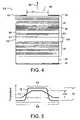
- FIG. 4illustrates one embodiment of a light generating device 100 of the present invention such as a VCSEL 100 .
- the VCSEL 100 of FIG. 4includes many portions that are same as or similar to corresponding portions of the VCSEL 10 of FIG. 1 .
- portions of the VCSEL 100 of FIG. 4 that are same as or similar to corresponding portions of the VCSEL 10 of FIG. 1are assigned the same reference numerals and different portions are assigned different reference numerals.
- not all reference numerals illustrated for the VCSEL 10 of FIG. 1are reproduced for the VCSEL 100 of FIG. 4 even though corresponding portions are illustrated in FIG. 1 .
- the VCSEL 100includes a light generation layer 40 adapted to generate light having a first, known wavelength.
- the light generation layer 40generates light have a wavelength of approximately 1.3 microns.
- the light generation layer 40is sandwiched between a top reflector 20 above the light generation layer 40 and a bottom reflector 30 below the light generation layer 40 .
- a high thermal conductivity (HTC) layer 102is fabricated between the light generation layer 40 and one of the reflectors 20 or 30 .
- the HTC layer 102is placed between the light generation layer 40 and the bottom reflector 30 . It is also understood that the HTC layer 102 can also be placed between the light generation layer 40 and the top reflector 20 .
- the VCSEL 100 of FIG. 4is fabricated over a substrate 50 . Electrodes 52 and 54 connect, respectively, to the substrate 50 and the top reflector 20 to provide electrical contacts.
- the top reflector 20 and the bottom reflector 30are distributed Bragg reflectors (DBR) formed by repeating alternating layers, or pairs of layers where each layer of the pair has a different refractive index compared to the other layer of the pair.
- DBRdistributed Bragg reflectors
- the HTC layer 102has a high optical transparency and has relatively higher thermal conductivity (or lower thermal resistance) compared to the thermal conductivity of the reflectors 20 and 30 . Moreover, here, the HTC layer 102 is in thermal contact with the light generation layer 40 where most of the heat is directly generated. Therefore, the HTC layer 102 facilities the removal of and dissipation of heat from the light generation layer 40 . Thickness 104 of the HTC layer 102 can range widely depending on application and is typically an integer multiple of one-half wavelength thick.
- a half-wave layerbehaves optically almost as if it wasn't there at all. Accordingly, insertion of a half-wave HTC layer into a VCSEL structure adds the benefits of the HTC with little optical side effects.
- Half-wave layershave the further advantage in that their optical properties do not depend on whether the surrounding material has higher or lower refractive index.
- a quarter wave layersuch as is found in the DBRs, is optically reflective, and its behavior depends on the surrounding material. Quarter wave layers could be used for the HTC layer of the present invention, but the extra flexibility of the half-wave layer make it relatively more likely choice for the present invention at this time.
- the HTC layer 102can be as thin as 0.1 microns or as thick as several microns or more. Thicker HTC layers are more effective at heat removal, but also cause larger cavity mode volume, which can reduce the maximum modulation speed or efficiency of the VCSEL in some cases. Thus, the optimum thickness 104 of the HTC layer 102 would be determined by the detailed requirements of the particular VCSEL design and application.
- the HTC layer 102can be fabricated using any suitable material. In the illustrated embodiment, the HTC layer 102 is fabricated using Aluminum Arsenide which has a relatively high thermal conductivity as discussed above and illustrated in relation to FIG. 3 .
- FIG. 5illustrates a lateral temperature distribution curve 110 along the active region 40 of the VCSEL 100 of FIG. 4 .
- layer interval 42 irepresents and corresponds to the extent of the light generation layer 42 (of the VCSEL 100 of FIG. 4 )
- active interval 43 irepresents and corresponds to the extent of the active portion 43 of the light generation layer 42 (of the VCSEL 100 of FIG. 4 ) where most of the photons are generated.
- the lateral temperature distribution curve 70 from FIG. 2is reproduced in FIG. 5 for comparison with the lateral temperature distribution curve 110 .
- the lateral temperature distribution curve 110As expected, temperature is highest at the active interval 43 i and the temperature drops off at the edges of the active interval 43 i . However, the highest temperature shown by the temperature distribution curve 110 is lower than the highest temperature shown by the temperature distribution curve 70 thereby indicating that the active portion 43 of the VCSEL 100 of FIG. 4 runs cooler than the corresponding active portion 43 of the VCSEL 10 of FIG. 1 .
- temperature differential 112(for curve 110 ) between the temperature at the active interval 43 i and the temperature outside the active interval 43 i is relatively smaller than the temperature differential 72 (for curve 70 ). Furthermore, the temperature transition from the active interval 43 i to the temperature outside the active interval 43 i is smoother for the curve 110 compared to the corresponding temperature drop off for the curve 70 .
- the HTC layer 102 of the VCSEL 100aids in dissipation of heat generated within the light generation layer 40 allowing the VCSEL 100 (of FIG. 4 ) to operate cooler thereby alleviating or eliminating the problems associated with high temperatures and high temperature gradients within the light generation layer 40 of the VCSEL 10 (of FIG. 1 ).
- the DBR mirroris preferably designed for low voltage drop so it generates little parasitic heat of its own during operation of the device.
- One method for improving the electrical conductivity of a DBR stackis by incorporating a spatially varying profile of dopants to encourage current flow.
- Another approach normally combined with the firstis to insert a compositionally graded transition layer between each pair of alternating layers in the DBR mirror.
- the graded transition layerserves the function of spreading the bandgap change over a finite distance, which allows a carefully designed dopant profile to create a path of little electrical resistance.
- the graded layersare typically 100 to 300 angstroms thick. However, the graded composition transition layers are necessarily composed of material compositions between that of the alternating DBR layers.
- the DBR mirroris composed of alternating AlGaAs layers
- these graded transition layerscontain a fraction of their thickness comprised of the AlGaAs compositions with the highest thermal resistivity.
- the graded layerscontribute to the thermal resistance of the DBR mirror.
- FIG. 6illustrates another embodiment of a light generating device 100 a of the present invention such as a VCSEL 100 a .
- the VCSEL 100 a of FIG. 6includes many portions that are same as or similar to corresponding portions of the VCSEL 100 of FIG. 4 .
- portions of the VCSEL 100 a of FIG. 6 that are same as or similar to corresponding portions of the VCSEL 100 of FIG. 4are assigned the same reference numerals, similar but changed portions are assigned the same reference numerals accompanied by letter “a,” and different portions are assigned different reference numerals.
- not all reference numerals illustrated for the VCSEL 100 of FIG. 4are reproduced for the VCSEL 100 a of FIG. 6 even though corresponding portions are illustrated in FIG. 4 .
- the VCSEL 100 ahas essentially the same structure as the VCSEL 100 of FIG. 4 except for the following modifications: Firstly, the VCSEL 100 a includes a non-doped bottom DBR mirror 30 a while its top DBR mirror 20 is doped with a p-type dopant. Thus, the electrical current from the top electrode 54 flows downward through the p-doped DBR mirror 20 and the light generation layer 40 , then laterally through a contact layer 106 , and finally out the lower contact 52 a.
- the contact layer 106can be fabricated using any material that can be rendered electrically conductive, optically transparent, and upon which a high quality light generation can be grown or deposited. Typical choices include GaAs, AlGaAs, InGaP, InGaAs, InP, AlInGaP or related materials or combinations of those materials.
- the contact layercan be made anywhere from, for example, 100 angstroms to several microns thick, though a typical heavily doped contact layer would be only several hundred angstroms thick to minimize optical losses and would typically be combined with a more lightly doped current spreading region of several thousand angstrom thickness comprising the total layer 106 .
- the HTC layer 102may also act as a current spreading layer to aid the lateral electrical conductivity of the contact layer.
- the lower n-type contacthas been moved from the bottom of the structure up to the contact layer just below the active region in this implementation, to allow the lower DBR mirror to be undoped and ungraded.
- the mirrorBy eliminating the need for graded layers at the interfaces of the alternating DBR layers, the mirror itself can be made with much higher thermal conductivity. However, removing the graded layers would cause very high voltage drop at those interfaces and corresponding parasitic heat generation, so the electrical conduction path circumvents the DBR mirror such as provided by contact and spreading layers 106 and 102 .
- the substrate 50 aneed not be doped as the substrate 50 of FIG. 1 .
- the contact layer 106may be separated from the light generation layer 40 using an etch-stop layer 108 .
- the etch-stop layer 108can be fabricated using many different materials such as InGaAs, InGaP, InP, AlInGaP or even GaAs or AlAs or related materials.
- the purpose of the etch stop layeris to add processing robustness for removing the upper layers 20 and 40 and stopping precisely on the contact layer 106 . Accordingly, the etch stop layer is normally quite thin, typically only a few hundred angstroms in thickness.
- the functions of layers 108 , 106 and 102may be combined into one or two layers.
- FIG. 7Aillustrates another embodiment of a light generating device 100 b of the present invention such as a VCSEL 100 b .
- the VCSEL 100 b of FIG. 7Aincludes many portions that are same as or similar to corresponding portions of the VCSEL 100 of FIG. 4 .
- portions of the VCSEL 100 b of FIG. 7A that are same as or similar to corresponding portions of the VCSEL 100 of FIG. 4are assigned the same reference numerals, similar but changed portions are assigned the same reference numerals accompanied by letter “b,” and different portions are assigned different reference numerals.
- not all reference numerals illustrated for the VCSEL 100 of FIG. 4are reproduced for the VCSEL 100 b of FIG. 7A even though corresponding portions are illustrated in FIG. 4 .
- the VCSEL 100 bhas essentially the same structure as the VCSEL 100 of FIG. 4 except that, in the VCSEL 100 b its HTC layer 102 b is positioned between the light generation layer 40 and the top DBR mirror 20 .
- the HTC layer 102 bis made of same or similar material and has similar configuration and structure as the HTC layer 102 of FIG. 4 .
- FIG. 7Billustrates another embodiment of a light generating device 100 c of the present invention such as a VCSEL 100 c .
- the VCSEL 100 c of FIG. 7Bincludes many portions that are same as or similar to corresponding portions of the VCSEL 100 a of FIG. 6 and the VCSEL 100 b of FIG. 7A .
- portions of the VCSEL 100 b of FIG. 7A that are same as or similar to corresponding portions of the VCSEL 100 a of FIG. 6 and/or the VCSEL 100 b of FIG. 7Aare assigned the same reference numerals, similar but changed portions are assigned the same reference numerals accompanied by letter “c,” and different portions are assigned different reference numerals.
- the VCSEL 100 chas essentially the same structure as the VCSEL 100 b of FIG. 7A except for the following modifications: Firstly, the VCSEL 100 c includes a non-doped bottom DBR mirror 30 a while its top DBR mirror 20 is doped with a p-type dopant. Thus, the electrical current from the top electrode 54 flows through the p-doped DBR mirror 20 , the HTC layer 102 b , the light generation layer 40 , and a contact layer 106 that is doped with n-type dopants.
- the contact layer 106would be similar to the corresponding layer 106 in VCSEL 100 a , and would have similar composition and thickness.
- the contact layer 106is adapted to provide electronic contact between an electrode and the light generation layer 40 .
- the contact layer 106is typically separated from the light generation layer 108 using an etch-stop layer 108 .
- the etch-stop layer 108has similar properties as the corresponding layer in VCSEL 100 a of FIG. 6 .
- FIG. 8Aillustrates another embodiment of a light generating device 100 d of the present invention such as a VCSEL 100 d .
- the VCSEL 100 d of FIG. 8Aincludes many portions that are same as or similar to corresponding portions of the VCSEL 10 of FIG. 1 .
- portions of the VCSEL 100 d of FIG. 8A that are same as or similar to corresponding portions of the VCSEL 10 of FIG. 1are assigned the same reference numerals, similar but changed portions are assigned the same reference numerals accompanied by letter “d,” and different portions are assigned different reference numerals.
- not all reference numerals illustrated for the VCSEL 10 of FIG. 1are reproduced for the VCSEL 100 d of FIG. 8A even though corresponding portions are illustrated in FIG. 1 .
- the VCSEL 100 dincludes a light generation layer 40 adapted to generate light having a first known wavelength.
- the light generation layer 40generates light have a wavelength of approximately 1.3 microns.
- the light generation layer 40is sandwiched between a top reflector 20 above the light generation layer 40 and a high thermal conductivity (HTC) bottom reflector 120 below the light generation layer 40 .
- HTChigh thermal conductivity
- the VCSEL 100 d of FIG. 8Ais fabricated over a substrate 50 . Electrodes 52 and 54 connect, respectively, to the substrate 50 and the top reflector 20 to provide electrical contacts.
- the top reflector 20 and the high thermal conductivity (HTC) bottom reflector 120are distributed Bragg reflectors (DBR) formed by repeating alternating layers, or pairs of layers where each layer of the pair has a different refractive index compared to the other layer of the pair.
- DBRdistributed Bragg reflectors
- the top DBR mirror 20is doped with p-type dopant and the bottom DBR mirror 30 is doped with n-type dopant in this embodiment.
- the top reflector 20 of the VCSEL 100 d of FIG. 8Ais configured as the top reflector 20 of the VCSEL 10 of FIG. 1 .
- the HTC bottom reflector 120includes pairs of layers where each pair has a first layer having a first thermal conductivity and a first thickness and a second layer having a second thermal conductivity and having a second thickness.
- the HTC bottom reflector 120includes, for example, a first pair 122 of layers.
- the first pair 122 of layerincludes a first layer 121 having a first thermal conductivity and a first thickness and a second layer 123 having a second thermal conductivity and a second thickness.
- the first layer 121can be, for example, Al (0.2) Ga (0.8) As having a thermal resistivity of approximately a little over six cm K/W as discussed before.
- the first layercan have a thickness that is an odd multiple of quarter wavelength including being quarter wavelength thick (one times quarter wavelength).
- the second layer 123can be, for example, Al (0.9) Ga (0.1) As having a thermal resistivity of approximately four cm K/W as discussed before or even AlAs having thermal resistivity of approximately four cm K/W as illustrated in FIG. 3 .
- the second layercan have a second thickness that is an odd multiple of quarter wavelength, for example, three times the quarter wavelength thick.
- the underlying concept for the design of the VCSEL 100 dis to fabricate the HTC bottom reflector 120 such that it has a higher proportion of material having a relatively higher thermal conductivity (lower thermal resistivity) compared to material having a relatively lower thermal conductivity (higher thermal resistivity).
- the resulting HTC bottom reflector 120has, as a whole, higher thermal conductivity (lower thermal resistivity) compared to the thermal conductivity of the bottom reflector 30 of FIG. 1 .
- the HTC bottom reflector 120has uniform HTC layer pairs. That is, as illustrated in FIG. 8A , each pair of layers of the HTC bottom reflector 120 is similarly configured with a first layer of each pair being quarter wavelength thick with a second layer of each pair being a same odd multiple of quarter wavelength thick, for example three times the quarter wavelength thick.
- FIGS. 8B and 8Cillustrate alternative embodiments of HTC bottom reflector 120 of FIG. 8A as HTC bottom reflectors 120 b and 120 c .
- the HTC bottom reflector 120 bincludes non-uniform HTC layer pairs. That is, as illustrated in FIG. 8B , a first HTC layer pair 122 of layers of the HTC bottom reflector 120 b is configured as the first pair 122 illustrated in FIG. 8A and described above. That is, the first pair 122 of layer includes a first layer 121 having a first thermal conductivity and a first thickness and a second layer 123 having a second thermal conductivity and a second thickness.
- the first layer 121can be, for example, Al (0.2) Ga (0.8) As having a thermal resistivity of approximately a little over six cm K/W as discussed before.
- the first layercan have a thickness that is an odd multiple of quarter wavelength including being quarter wavelength thick (one times quarter wavelength).
- the second layer 123can be, for example, Al (0.9) Ga (0.1) As having a thermal resistivity of approximately four cm K/W as discussed before or even AlAs having thermal resistivity of approximately four cm K/W as illustrated in FIG. 3 .
- the second layercan have a thickness that is an odd multiple of quarter wavelength, for example, three times the quarter wavelength thick.
- the HTC bottom reflector 120 balso includes a second HTC layer pair 32 of layers that is configured similar to the pair 32 of layers of VCSEL 10 of FIG. 1 .
- the second pair 32 of layersincludes a third layer 31 having the same thermal conductivity (first thermal conductivity) and the same thickness (first thickness) as the first layer 121 .
- the second pair 32 of layersfurther includes a fourth layer 33 having the same thermal conductivity (second thermal conductivity) as the second layer 123 but having the same thickness (first thickness) as the first layer 121 .
- the HTC bottom reflector 120 cincludes another configuration of non-uniform HTC layer pairs.
- a first HTC layer pair 122 of layers of the HTC bottom reflector 120 cis configured as the first pair 122 illustrated in FIG. 8A and described above.
- the HTC bottom reflector 120 calso includes a second HTC layer pair 32 configured similar to the pair 32 of layers illustrated in FIG. 8B and described above.
- the HTC bottom reflector 120 cfurther includes a third HTC layer pair 126 including a fifth layer 125 having the same thermal conductivity (first thermal conductivity) and the same thickness (first thickness) as the first layer 121 .
- the third pair 126 of layersalso includes a sixth layer 127 having the same thermal conductivity (second thermal conductivity) as the second layer 123 but having a third thickness that is an odd multiple of quarter wavelength, for example, five times the quarter wavelength thick.
- optically pumped lasersnormally generate heat in the light generating layer creating a temperature profile and heat flow very similar to that described for the electrically pumped VCSEL here, and would benefit from the same types of HTC layer configurations.
- a second exampleis a resonant cavity LED, an electrically pumped semiconductor device similar to a VCSEL described here, but which does not achieve a lasing state.
- the maximum output power of the resonant cavity LEDis limited by heat generation much like a VCSEL, and the device would benefit in the same way from the same types of HTC layer configurations described here.
- the present inventionis novel and offers advantages over the current art.
- specific embodiments of the inventionare described and illustrated above, the invention is not to be limited to the specific forms or arrangements of parts so described and illustrated.
- the HTC reflectorcan be fabricated as the top reflector 20 instead of or in addition to the HTC bottom reflector 120 .
- different materialscan be used instead of or in addition to various compositions of AlGaAs but still fall within the scope of the present invention. The invention is limited by the claims that follow.
Landscapes
- Physics & Mathematics (AREA)
- Condensed Matter Physics & Semiconductors (AREA)
- General Physics & Mathematics (AREA)
- Electromagnetism (AREA)
- Optics & Photonics (AREA)
- Semiconductor Lasers (AREA)
Abstract
Description
AlxGa(1-x)As
where X is a composition ratio of Aluminum and Gallium. For example, when X is zero, there is no Aluminum in the composition and the composition reduces to GaAs. When X is one (1), there is no Gallium in the composition, and the composition reduces to AlAs. When X is 0.3, for example, then the composition can be expressed as Al(0.3)Ga(0.7)As. In
Claims (10)
Priority Applications (5)
| Application Number | Priority Date | Filing Date | Title |
|---|---|---|---|
| US10/862,753US7372886B2 (en) | 2004-06-07 | 2004-06-07 | High thermal conductivity vertical cavity surface emitting laser (VCSEL) |
| DE102005010933ADE102005010933B4 (en) | 2004-06-07 | 2005-03-09 | Surface emitting vertical cavity laser (VCSEL) with high thermal conductivity |
| CNB2005100752165ACN100574026C (en) | 2004-06-07 | 2005-06-07 | High Thermal Conductivity Vertical Cavity Surface Emitting Laser |
| JP2005166540AJP5063869B2 (en) | 2004-06-07 | 2005-06-07 | Vertical cavity surface emitting laser with high thermal conductivity |
| US11/503,717US20060274805A1 (en) | 2004-06-07 | 2006-08-14 | High thermal conductivity vertical cavity surface emitting laser (VCSEL) |
Applications Claiming Priority (1)
| Application Number | Priority Date | Filing Date | Title |
|---|---|---|---|
| US10/862,753US7372886B2 (en) | 2004-06-07 | 2004-06-07 | High thermal conductivity vertical cavity surface emitting laser (VCSEL) |
Related Child Applications (1)
| Application Number | Title | Priority Date | Filing Date |
|---|---|---|---|
| US11/503,717DivisionUS20060274805A1 (en) | 2004-06-07 | 2006-08-14 | High thermal conductivity vertical cavity surface emitting laser (VCSEL) |
Publications (2)
| Publication Number | Publication Date |
|---|---|
| US20050271113A1 US20050271113A1 (en) | 2005-12-08 |
| US7372886B2true US7372886B2 (en) | 2008-05-13 |
Family
ID=35448893
Family Applications (2)
| Application Number | Title | Priority Date | Filing Date |
|---|---|---|---|
| US10/862,753Expired - LifetimeUS7372886B2 (en) | 2004-06-07 | 2004-06-07 | High thermal conductivity vertical cavity surface emitting laser (VCSEL) |
| US11/503,717AbandonedUS20060274805A1 (en) | 2004-06-07 | 2006-08-14 | High thermal conductivity vertical cavity surface emitting laser (VCSEL) |
Family Applications After (1)
| Application Number | Title | Priority Date | Filing Date |
|---|---|---|---|
| US11/503,717AbandonedUS20060274805A1 (en) | 2004-06-07 | 2006-08-14 | High thermal conductivity vertical cavity surface emitting laser (VCSEL) |
Country Status (4)
| Country | Link |
|---|---|
| US (2) | US7372886B2 (en) |
| JP (1) | JP5063869B2 (en) |
| CN (1) | CN100574026C (en) |
| DE (1) | DE102005010933B4 (en) |
Cited By (5)
| Publication number | Priority date | Publication date | Assignee | Title |
|---|---|---|---|---|
| US20080043798A1 (en)* | 2003-03-24 | 2008-02-21 | The University Of Strathclyde | Vertical-Cavity Semiconductor Optical Devices |
| US20110037825A1 (en)* | 2008-05-02 | 2011-02-17 | Ricoh Company, Ltd. | Vertical cavity surface emitting laser device, vertical cavity surface emitting laser array, optical scanning apparatus, image forming apparatus, optical transmission module and optical transmission system |
| US8319973B2 (en) | 2009-04-08 | 2012-11-27 | Honeywell International Inc. | VCSEL enabled active resonator gyroscope |
| US10361531B2 (en) | 2014-02-25 | 2019-07-23 | Philips Photonics Gmbh | Light emitting semiconductor devices with getter layer |
| US20210167579A1 (en)* | 2019-11-29 | 2021-06-03 | Ricoh Company, Ltd. | Surface emitting laser, surface emitting laser device, light source device, and detection apparatus |
Families Citing this family (37)
| Publication number | Priority date | Publication date | Assignee | Title |
|---|---|---|---|---|
| US7372886B2 (en)* | 2004-06-07 | 2008-05-13 | Avago Technologies Fiber Ip Pte Ltd | High thermal conductivity vertical cavity surface emitting laser (VCSEL) |
| JP4908837B2 (en)* | 2005-12-13 | 2012-04-04 | キヤノン株式会社 | Light emitting element array and image forming apparatus |
| JP2013030790A (en)* | 2006-02-03 | 2013-02-07 | Ricoh Co Ltd | Surface light emitting laser element, surface light emitting laser array having the element, image forming apparatus having the array, optical pick-up device having the element or array, optical transmission module having the element or array, optical transmission/reception module having the element or array, and optical communication system having the element or array |
| JP5224155B2 (en)* | 2006-02-03 | 2013-07-03 | 株式会社リコー | Surface emitting laser element, surface emitting laser array including the same, image forming apparatus including surface emitting laser array, surface pickup laser element or optical pickup apparatus including surface emitting laser array, surface emitting laser element or surface emitting laser array An optical transmission module comprising: an optical transmission / reception module comprising a surface emitting laser element or a surface emitting laser array; and an optical communication system comprising a surface emitting laser element or a surface emitting laser array. |
| KR100922401B1 (en)* | 2006-02-03 | 2009-10-19 | 가부시키가이샤 리코 | Surface-emitting laser device and surface-emitting laser array including same |
| US7693204B2 (en)* | 2006-02-03 | 2010-04-06 | Ricoh Company, Ltd. | Surface-emitting laser device and surface-emitting laser array including same |
| WO2007103527A2 (en)* | 2006-03-07 | 2007-09-13 | Brenner Mary K | Red light laser |
| JP2007299897A (en)* | 2006-04-28 | 2007-11-15 | Ricoh Co Ltd | Surface emitting laser element, surface emitting laser array including the same, image forming apparatus including surface emitting laser element or surface emitting laser array, optical interconnection system including surface emitting laser element or surface emitting laser array, and surface emitting laser Optical communication system with element or surface emitting laser array |
| JP5447719B2 (en)* | 2006-08-23 | 2014-03-19 | 株式会社リコー | Surface emitting laser array, optical scanning device and image forming apparatus provided with the same |
| JP2008060322A (en)* | 2006-08-31 | 2008-03-13 | Ricoh Co Ltd | Surface emitting laser element, surface emitting laser array, optical scanning device, image forming apparatus, and optical communication system |
| US9461201B2 (en) | 2007-11-14 | 2016-10-04 | Cree, Inc. | Light emitting diode dielectric mirror |
| US7915629B2 (en)* | 2008-12-08 | 2011-03-29 | Cree, Inc. | Composite high reflectivity layer |
| US7839913B2 (en)* | 2007-11-22 | 2010-11-23 | Canon Kabushiki Kaisha | Surface emitting laser, surface emitting laser array, and image forming apparatus including surface emitting laser |
| DE102008014193A1 (en) | 2008-03-14 | 2009-09-24 | Universität Stuttgart | Vertical resonator laser |
| JP2009277781A (en)* | 2008-05-13 | 2009-11-26 | Ricoh Co Ltd | Surface light emission type laser array element, optical scanning apparatus, and image forming apparatus |
| JP5262293B2 (en) | 2008-05-26 | 2013-08-14 | 三菱電機株式会社 | Optical semiconductor device |
| JP2009290161A (en)* | 2008-06-02 | 2009-12-10 | Mitsubishi Electric Corp | Optical semiconductor device |
| US9362459B2 (en) | 2009-09-02 | 2016-06-07 | United States Department Of Energy | High reflectivity mirrors and method for making same |
| US9435493B2 (en) | 2009-10-27 | 2016-09-06 | Cree, Inc. | Hybrid reflector system for lighting device |
| JP5721051B2 (en)* | 2011-03-09 | 2015-05-20 | 株式会社リコー | Surface emitting laser element, surface emitting laser array, optical scanning device, and image forming apparatus |
| US9728676B2 (en) | 2011-06-24 | 2017-08-08 | Cree, Inc. | High voltage monolithic LED chip |
| US10243121B2 (en) | 2011-06-24 | 2019-03-26 | Cree, Inc. | High voltage monolithic LED chip with improved reliability |
| JP5857707B2 (en)* | 2011-12-14 | 2016-02-10 | 日亜化学工業株式会社 | Surface emitting laser element |
| CN102868091A (en)* | 2012-09-13 | 2013-01-09 | 北京工业大学 | High-power surface-emitting laser using graphene surface current extension layer |
| US9014225B2 (en) | 2013-09-18 | 2015-04-21 | Sae Magnetics (H.K.) Ltd. | Vertical cavity surface emitting laser device |
| JP2015076425A (en)* | 2013-10-07 | 2015-04-20 | 富士ゼロックス株式会社 | Surface-emitting semiconductor laser, surface-emitting semiconductor laser array, surface-emitting semiconductor laser device, optical transmission device, information processing equipment, and method of manufacturing surface-emitting semiconductor laser |
| JP2015115377A (en)* | 2013-12-10 | 2015-06-22 | 株式会社リコー | COMPOUND SEMICONDUCTOR DEVICE, LIGHT SOURCE DEVICE, LASER DEVICE, AND COMPOUND SEMICONDUCTOR DEVICE MANUFACTURING METHOD |
| US10439360B1 (en)* | 2014-12-04 | 2019-10-08 | Ii-Vi Delaware, Inc. | VCSEL with emission on substrate side |
| US10658546B2 (en) | 2015-01-21 | 2020-05-19 | Cree, Inc. | High efficiency LEDs and methods of manufacturing |
| KR102496476B1 (en)* | 2015-11-19 | 2023-02-06 | 삼성전자주식회사 | Electromagnetic wave reflector and optical device including the same |
| JP2017216348A (en)* | 2016-05-31 | 2017-12-07 | 三菱電機株式会社 | End face emission type semiconductor laser |
| TWI805824B (en)* | 2018-08-13 | 2023-06-21 | 新加坡商Ams傳感器亞洲私人有限公司 | Low divergence vertical cavity surface emitting lasers, and modules and host devices incorporating the same |
| JP7095498B2 (en)* | 2018-08-31 | 2022-07-05 | 住友電気工業株式会社 | Method for manufacturing a vertical resonance type surface emitting laser and a vertical resonance type surface emitting laser |
| CN109728502B (en)* | 2019-01-08 | 2020-07-31 | 扬州乾照光电有限公司 | Vertical cavity surface emitting laser epitaxial structure and preparation method thereof |
| WO2020150060A1 (en)* | 2019-01-17 | 2020-07-23 | Array Photonics, Inc. | Control of vcsel spatial modes and output beam |
| CN112260062A (en)* | 2020-09-10 | 2021-01-22 | 华芯半导体科技有限公司 | Vertical cavity surface emitting laser and preparation method thereof |
| CN113725729B (en)* | 2021-09-02 | 2022-12-20 | 厦门市三安集成电路有限公司 | High-heat-dissipation vertical-cavity surface-emitting laser and manufacturing method thereof |
Citations (37)
| Publication number | Priority date | Publication date | Assignee | Title |
|---|---|---|---|---|
| US5557626A (en) | 1994-06-15 | 1996-09-17 | Motorola | Patterned mirror VCSEL with adjustable selective etch region |
| US5596595A (en) | 1995-06-08 | 1997-01-21 | Hewlett-Packard Company | Current and heat spreading transparent layers for surface-emitting lasers |
| US5727014A (en) | 1995-10-31 | 1998-03-10 | Hewlett-Packard Company | Vertical-cavity surface-emitting laser generating light with a defined direction of polarization |
| US5729563A (en) | 1994-07-07 | 1998-03-17 | Hewlett-Packard Company | Method and apparatus for optically and thermally isolating surface emitting laser diodes |
| US5818861A (en) | 1996-07-19 | 1998-10-06 | Hewlett-Packard Company | Vertical cavity surface emitting laser with low band gap highly doped contact layer |
| US5838708A (en) | 1994-10-31 | 1998-11-17 | Hewlett-Packard Company | Integration of surface emitting laser and photodiode for monitoring power output of surface emitting laser |
| US5838715A (en) | 1996-06-20 | 1998-11-17 | Hewlett-Packard Company | High intensity single-mode VCSELs |
| US5867516A (en) | 1996-03-12 | 1999-02-02 | Hewlett-Packard Company | Vertical cavity surface emitting laser with reduced turn-on jitter and increased single-mode output |
| US5892787A (en) | 1994-10-27 | 1999-04-06 | Hewlett-Packard Company | N-drive, p-common light-emitting devices fabricated on an n-type substrate and method of making same |
| US5892784A (en) | 1994-10-27 | 1999-04-06 | Hewlett-Packard Company | N-drive p-common surface emitting laser fabricated on n+ substrate |
| US6069908A (en) | 1998-02-09 | 2000-05-30 | Hewlwtt-Packard Company | N-drive or P-drive VCSEL array |
| US6133589A (en) | 1999-06-08 | 2000-10-17 | Lumileds Lighting, U.S., Llc | AlGaInN-based LED having thick epitaxial layer for improved light extraction |
| US6188711B1 (en) | 1997-12-18 | 2001-02-13 | Agilent Technologies, Inc. | Polarization-controlled VCSELs using externally applied uniaxial stress |
| US6252896B1 (en) | 1999-03-05 | 2001-06-26 | Agilent Technologies, Inc. | Long-Wavelength VCSEL using buried bragg reflectors |
| WO2002017445A1 (en) | 2000-08-22 | 2002-02-28 | Regents Of The University Of California, The | Heat spreading layers for vertical cavity surface emitting lasers |
| US20020101899A1 (en) | 2000-11-28 | 2002-08-01 | Noriyuki Yokouchi | Vertical cavity surface emitting laser device |
| EP1246328A2 (en) | 2001-03-15 | 2002-10-02 | Agilent Technologies, Inc. (a Delaware corporation) | Intracavity contacted long wavelength VCSELs with buried antimony layers |
| US20030039284A1 (en)* | 2001-08-16 | 2003-02-27 | Jun Zheng | VCSEL with heat-spreading layer |
| US6570190B2 (en) | 1997-06-03 | 2003-05-27 | Lumileds Lighting, U.S., Llc | LED having angled sides for increased side light extraction |
| US20030112517A1 (en) | 2001-12-14 | 2003-06-19 | Corzine Scott W. | Distributed bragg reflector and method of fabrication |
| US20030123505A1 (en) | 2001-12-31 | 2003-07-03 | Peters Frank H. | Optoelectronic device using a disabled tunnel junction for current confinement |
| US20030128733A1 (en) | 2002-01-09 | 2003-07-10 | Tan Michael Renne Ty | Vertical-cavity surface-emitting laser including a supported airgap distributed Bragg reflector |
| US20030181024A1 (en) | 2002-03-25 | 2003-09-25 | Tetsuya Takeuchi | Method for obtaining high quality InGaAsN semiconductor devices |
| US20030179801A1 (en) | 2002-03-25 | 2003-09-25 | Tetsuya Takeuchi | Asymmetric InGaAsN vertical cavity surface emitting lasers |
| US20030185267A1 (en)* | 2002-03-28 | 2003-10-02 | Applied Optoelectronics, Inc. | VCSEL with antiguide current confinement layer |
| US6639931B1 (en) | 1997-05-17 | 2003-10-28 | University Of Bristol | Laser devices |
| US6647050B2 (en) | 2001-09-18 | 2003-11-11 | Agilent Technologies, Inc. | Flip-chip assembly for optically-pumped lasers |
| US6650684B1 (en) | 1994-07-08 | 2003-11-18 | Agilent Technologies, Inc. | Surface emitting laser diodes with enhanced higher order spatial modes and/or filamentation |
| US20040066819A1 (en) | 2000-11-28 | 2004-04-08 | Johnson Ralph H. | Versatile method and system for single mode VCSELs |
| US6720585B1 (en)* | 2001-01-16 | 2004-04-13 | Optical Communication Products, Inc. | Low thermal impedance DBR for optoelectronic devices |
| US20040075908A1 (en) | 2002-10-16 | 2004-04-22 | Chen Fei Chuang | Multilayer mirror |
| US20040161004A1 (en)* | 2003-02-18 | 2004-08-19 | Eastman Kodak Company | Organic laser having improved linearity |
| US20040179568A1 (en)* | 2001-02-15 | 2004-09-16 | Markus-Christian Amann | Surface-emitting semiconductor laser |
| US20040208216A1 (en)* | 2001-04-11 | 2004-10-21 | Naone Ryan Likeke | Long wavelength vertical cavity surface emitting laser |
| US6810064B1 (en)* | 2000-08-22 | 2004-10-26 | The Regents Of The University Of California | Heat spreading layers for vertical cavity surface emitting lasers |
| US6959025B2 (en)* | 2002-02-22 | 2005-10-25 | Ricoh Company, Ltd. | Surface-emitting laser diode having reduced device resistance and capable of performing high output operation, surface-emitting laser diode array, electrophotographic system, surface-emitting laser diode module, optical telecommunication system, optical interconnection system using the surface-emitting laser diode, and method of fabricating the surface-emitting laser diode |
| US20050271113A1 (en)* | 2004-06-07 | 2005-12-08 | Song Yoon K | High thermal conductivity vertical cavity surface emitting laser (VCSEL) |
Family Cites Families (23)
| Publication number | Priority date | Publication date | Assignee | Title |
|---|---|---|---|---|
| US5144681A (en)* | 1989-03-31 | 1992-09-01 | Dainnippon Screen Mfg. Co., Ltd. | Method of and apparatus for inspecting conductive pattern on printed board |
| US5111406A (en)* | 1990-01-05 | 1992-05-05 | Nicolet Instrument Corporation | Method for determining drill target locations in a multilayer board panel |
| DE4027994A1 (en)* | 1990-09-04 | 1992-03-05 | Gw Elektronik Gmbh | HF MAGNETIC COIL ARRANGEMENT AND METHOD FOR THEIR PRODUCTION |
| JP2500529B2 (en)* | 1990-12-28 | 1996-05-29 | 日本電気株式会社 | Flat optical semiconductor device |
| US5250843A (en)* | 1991-03-27 | 1993-10-05 | Integrated System Assemblies Corp. | Multichip integrated circuit modules |
| JPH0513872A (en)* | 1991-07-05 | 1993-01-22 | Sony Corp | Hetero junction type semiconductor laser |
| US5282312A (en)* | 1991-12-31 | 1994-02-01 | Tessera, Inc. | Multi-layer circuit construction methods with customization features |
| US5337151A (en)* | 1992-07-28 | 1994-08-09 | Optical Radiation Corporation | Double-sided circuit board exposure machine and method with optical registration and material variation compensation |
| US5266380A (en)* | 1992-09-08 | 1993-11-30 | Motorola, Inc. | Method and apparatus for visual verification of proper assembly and alignment of layers in a multi-layer printed circuit board |
| WO1994008443A1 (en)* | 1992-09-29 | 1994-04-14 | Berg N Edward | Method and apparatus for fabricating printed circuit boards |
| US5355247A (en)* | 1993-03-30 | 1994-10-11 | The Board Of Trustees Of The Leland Stanford, Jr. University | Method using a monolithic crystalline material for producing radiation by quasi-phase-matching, diffusion bonded monolithic crystalline material for quasi-phase-matching, and method for fabricating same |
| US5393359A (en)* | 1993-08-10 | 1995-02-28 | Industrial Technology Research Institute | Method and apparatus for bonding outer leads of a liquid crystal display to metal leads of a bonding tape |
| US5403684A (en)* | 1993-08-11 | 1995-04-04 | Cray Research, Inc. | PCB tooling apparatus and method for forming patterns in registration on both sides of a substrate |
| US5655030A (en)* | 1993-12-27 | 1997-08-05 | Uht Corporation | Method for detecting the center of target marks by image processing |
| CA2301351C (en)* | 1994-11-28 | 2002-01-22 | Advanced Cardiovascular Systems, Inc. | Method and apparatus for direct laser cutting of metal stents |
| US5764485A (en)* | 1996-04-19 | 1998-06-09 | Lebaschi; Ali | Multi-layer PCB blockade-via pad-connection |
| US5838745A (en)* | 1996-10-09 | 1998-11-17 | Ericsson Inc. | Synchronization method, and associated circuitry, for improved synchronization of a receiver with a transmitter using nonlinear transformation metrics |
| US6091026A (en)* | 1996-11-30 | 2000-07-18 | Samsung Electro-Mechanics Co. Ltd. | Multi-layer printed circuit board with human detectable layer misregistration, and manufacturing method therefor |
| US5898227A (en)* | 1997-02-18 | 1999-04-27 | International Business Machines Corporation | Alignment targets having enhanced contrast |
| JPH10233558A (en)* | 1997-02-19 | 1998-09-02 | Canon Inc | Multilayer film structure including diamond layer, optical device having the same, and method of manufacturing the same |
| JP2003133638A (en)* | 2001-08-14 | 2003-05-09 | Furukawa Electric Co Ltd:The | Distributed feedback semiconductor laser device and laser module |
| DE10147888A1 (en)* | 2001-09-28 | 2003-04-24 | Osram Opto Semiconductors Gmbh | Optically pumped vertically emitting semiconductor laser |
| JP2004146515A (en)* | 2002-10-23 | 2004-05-20 | Furukawa Electric Co Ltd:The | Semiconductor laser device |
- 2004
- 2004-06-07USUS10/862,753patent/US7372886B2/ennot_activeExpired - Lifetime
- 2005
- 2005-03-09DEDE102005010933Apatent/DE102005010933B4/ennot_activeExpired - Fee Related
- 2005-06-07JPJP2005166540Apatent/JP5063869B2/ennot_activeExpired - Fee Related
- 2005-06-07CNCNB2005100752165Apatent/CN100574026C/ennot_activeExpired - Fee Related
- 2006
- 2006-08-14USUS11/503,717patent/US20060274805A1/ennot_activeAbandoned
Patent Citations (39)
| Publication number | Priority date | Publication date | Assignee | Title |
|---|---|---|---|---|
| US5557626A (en) | 1994-06-15 | 1996-09-17 | Motorola | Patterned mirror VCSEL with adjustable selective etch region |
| US5729563A (en) | 1994-07-07 | 1998-03-17 | Hewlett-Packard Company | Method and apparatus for optically and thermally isolating surface emitting laser diodes |
| US6650684B1 (en) | 1994-07-08 | 2003-11-18 | Agilent Technologies, Inc. | Surface emitting laser diodes with enhanced higher order spatial modes and/or filamentation |
| US5892787A (en) | 1994-10-27 | 1999-04-06 | Hewlett-Packard Company | N-drive, p-common light-emitting devices fabricated on an n-type substrate and method of making same |
| US5892784A (en) | 1994-10-27 | 1999-04-06 | Hewlett-Packard Company | N-drive p-common surface emitting laser fabricated on n+ substrate |
| US5838708A (en) | 1994-10-31 | 1998-11-17 | Hewlett-Packard Company | Integration of surface emitting laser and photodiode for monitoring power output of surface emitting laser |
| US5596595A (en) | 1995-06-08 | 1997-01-21 | Hewlett-Packard Company | Current and heat spreading transparent layers for surface-emitting lasers |
| US5727014A (en) | 1995-10-31 | 1998-03-10 | Hewlett-Packard Company | Vertical-cavity surface-emitting laser generating light with a defined direction of polarization |
| US5867516A (en) | 1996-03-12 | 1999-02-02 | Hewlett-Packard Company | Vertical cavity surface emitting laser with reduced turn-on jitter and increased single-mode output |
| US5838715A (en) | 1996-06-20 | 1998-11-17 | Hewlett-Packard Company | High intensity single-mode VCSELs |
| US5818861A (en) | 1996-07-19 | 1998-10-06 | Hewlett-Packard Company | Vertical cavity surface emitting laser with low band gap highly doped contact layer |
| US6639931B1 (en) | 1997-05-17 | 2003-10-28 | University Of Bristol | Laser devices |
| US6570190B2 (en) | 1997-06-03 | 2003-05-27 | Lumileds Lighting, U.S., Llc | LED having angled sides for increased side light extraction |
| US6188711B1 (en) | 1997-12-18 | 2001-02-13 | Agilent Technologies, Inc. | Polarization-controlled VCSELs using externally applied uniaxial stress |
| US6069908A (en) | 1998-02-09 | 2000-05-30 | Hewlwtt-Packard Company | N-drive or P-drive VCSEL array |
| US6252896B1 (en) | 1999-03-05 | 2001-06-26 | Agilent Technologies, Inc. | Long-Wavelength VCSEL using buried bragg reflectors |
| US6649440B1 (en) | 1999-06-08 | 2003-11-18 | Lumileds Lighting U.S., Llc | Aluminum indium gallium nitride-based LED having thick epitaxial layer for improved light extraction |
| US6133589A (en) | 1999-06-08 | 2000-10-17 | Lumileds Lighting, U.S., Llc | AlGaInN-based LED having thick epitaxial layer for improved light extraction |
| US6810064B1 (en)* | 2000-08-22 | 2004-10-26 | The Regents Of The University Of California | Heat spreading layers for vertical cavity surface emitting lasers |
| WO2002017445A1 (en) | 2000-08-22 | 2002-02-28 | Regents Of The University Of California, The | Heat spreading layers for vertical cavity surface emitting lasers |
| US6905900B1 (en)* | 2000-11-28 | 2005-06-14 | Finisar Corporation | Versatile method and system for single mode VCSELs |
| US20040066819A1 (en) | 2000-11-28 | 2004-04-08 | Johnson Ralph H. | Versatile method and system for single mode VCSELs |
| US20020101899A1 (en) | 2000-11-28 | 2002-08-01 | Noriyuki Yokouchi | Vertical cavity surface emitting laser device |
| US6720585B1 (en)* | 2001-01-16 | 2004-04-13 | Optical Communication Products, Inc. | Low thermal impedance DBR for optoelectronic devices |
| US20040179568A1 (en)* | 2001-02-15 | 2004-09-16 | Markus-Christian Amann | Surface-emitting semiconductor laser |
| EP1246328A2 (en) | 2001-03-15 | 2002-10-02 | Agilent Technologies, Inc. (a Delaware corporation) | Intracavity contacted long wavelength VCSELs with buried antimony layers |
| US20040208216A1 (en)* | 2001-04-11 | 2004-10-21 | Naone Ryan Likeke | Long wavelength vertical cavity surface emitting laser |
| US20030039284A1 (en)* | 2001-08-16 | 2003-02-27 | Jun Zheng | VCSEL with heat-spreading layer |
| US6647050B2 (en) | 2001-09-18 | 2003-11-11 | Agilent Technologies, Inc. | Flip-chip assembly for optically-pumped lasers |
| US20030112517A1 (en) | 2001-12-14 | 2003-06-19 | Corzine Scott W. | Distributed bragg reflector and method of fabrication |
| US20030123505A1 (en) | 2001-12-31 | 2003-07-03 | Peters Frank H. | Optoelectronic device using a disabled tunnel junction for current confinement |
| US20030128733A1 (en) | 2002-01-09 | 2003-07-10 | Tan Michael Renne Ty | Vertical-cavity surface-emitting laser including a supported airgap distributed Bragg reflector |
| US6959025B2 (en)* | 2002-02-22 | 2005-10-25 | Ricoh Company, Ltd. | Surface-emitting laser diode having reduced device resistance and capable of performing high output operation, surface-emitting laser diode array, electrophotographic system, surface-emitting laser diode module, optical telecommunication system, optical interconnection system using the surface-emitting laser diode, and method of fabricating the surface-emitting laser diode |
| US20030179801A1 (en) | 2002-03-25 | 2003-09-25 | Tetsuya Takeuchi | Asymmetric InGaAsN vertical cavity surface emitting lasers |
| US20030181024A1 (en) | 2002-03-25 | 2003-09-25 | Tetsuya Takeuchi | Method for obtaining high quality InGaAsN semiconductor devices |
| US20030185267A1 (en)* | 2002-03-28 | 2003-10-02 | Applied Optoelectronics, Inc. | VCSEL with antiguide current confinement layer |
| US20040075908A1 (en) | 2002-10-16 | 2004-04-22 | Chen Fei Chuang | Multilayer mirror |
| US20040161004A1 (en)* | 2003-02-18 | 2004-08-19 | Eastman Kodak Company | Organic laser having improved linearity |
| US20050271113A1 (en)* | 2004-06-07 | 2005-12-08 | Song Yoon K | High thermal conductivity vertical cavity surface emitting laser (VCSEL) |
Cited By (8)
| Publication number | Priority date | Publication date | Assignee | Title |
|---|---|---|---|---|
| US20080043798A1 (en)* | 2003-03-24 | 2008-02-21 | The University Of Strathclyde | Vertical-Cavity Semiconductor Optical Devices |
| US20110037825A1 (en)* | 2008-05-02 | 2011-02-17 | Ricoh Company, Ltd. | Vertical cavity surface emitting laser device, vertical cavity surface emitting laser array, optical scanning apparatus, image forming apparatus, optical transmission module and optical transmission system |
| US8891571B2 (en) | 2008-05-02 | 2014-11-18 | Ricoh Company, Ltd. | Vertical cavity surface emitting laser device, vertical cavity surface emitting laser array, optical scanning apparatus, image forming apparatus, optical transmission module and optical transmission system |
| US9570887B2 (en) | 2008-05-02 | 2017-02-14 | Ricoh Company, Ltd. | Vertical cavity surface emitting laser device, vertical cavity surface emitting laser array, optical scanning apparatus, image forming apparatus, optical transmission module and optical transmission system |
| US8319973B2 (en) | 2009-04-08 | 2012-11-27 | Honeywell International Inc. | VCSEL enabled active resonator gyroscope |
| US10361531B2 (en) | 2014-02-25 | 2019-07-23 | Philips Photonics Gmbh | Light emitting semiconductor devices with getter layer |
| US20210167579A1 (en)* | 2019-11-29 | 2021-06-03 | Ricoh Company, Ltd. | Surface emitting laser, surface emitting laser device, light source device, and detection apparatus |
| US12046872B2 (en)* | 2019-11-29 | 2024-07-23 | Ricoh Company, Ltd. | Surface emitting laser, surface emitting laser device, light source device, and detection apparatus |
Also Published As
| Publication number | Publication date |
|---|---|
| JP2005354061A (en) | 2005-12-22 |
| DE102005010933A1 (en) | 2005-12-29 |
| JP5063869B2 (en) | 2012-10-31 |
| DE102005010933B4 (en) | 2008-07-03 |
| US20060274805A1 (en) | 2006-12-07 |
| US20050271113A1 (en) | 2005-12-08 |
| CN1707889A (en) | 2005-12-14 |
| CN100574026C (en) | 2009-12-23 |
Similar Documents
| Publication | Publication Date | Title |
|---|---|---|
| US7372886B2 (en) | High thermal conductivity vertical cavity surface emitting laser (VCSEL) | |
| US6653158B2 (en) | Double intracavity contacted long-wavelength VCSELs and method of fabricating same | |
| US11424597B2 (en) | Tunnel junction for GaAs based VCSELs and method therefor | |
| Karim et al. | Long-wavelength vertical-cavity lasers and amplifiers | |
| Haglund et al. | High-speed VCSELs with strong confinement of optical fields and carriers | |
| US9014225B2 (en) | Vertical cavity surface emitting laser device | |
| US8031752B1 (en) | VCSEL optimized for high speed data | |
| JP4177262B2 (en) | Asymmetric distributed Bragg reflector for vertical cavity surface emitting lasers | |
| JP5029254B2 (en) | Surface emitting laser | |
| US6882673B1 (en) | Mirror structure for reducing the effect of feedback on a VCSEL | |
| Karim et al. | 1.55-/spl mu/m vertical-cavity laser arrays for wavelength-division multiplexing | |
| Lee et al. | Deep-red continuous wave top-surface-emitting vertical-cavity AlGaAs superlattice lasers | |
| Fan et al. | 10.1 nm range continuous wavelength-tunable vertical-cavity surface-emitting lasers | |
| WO2004064211A1 (en) | Laser array | |
| Larson et al. | Low-threshold oxide-confined GaInNAs long wavelength vertical cavity lasers | |
| US6810064B1 (en) | Heat spreading layers for vertical cavity surface emitting lasers | |
| Chang‐Hasnain et al. | Effect of operating electric power on the dynamic behavior of quantum well vertical‐cavity surface‐emitting lasers | |
| Hadley | Vertical-cavity surface-emitting laser diodes: design, growth, mode control and integration by fluidic self-assembly | |
| Kawakami et al. | Low-threshold current low-voltage vertical-cavity surface-emitting lasers with low-Al-content p-type mirrors grown by MOCVD | |
| Strijbos et al. | Current crowding in oxide-confined intracavity-contacted VCSELs | |
| Karim et al. | Design and performance analysis of GaInNAsSb/GaAs MQW VCSEL operating at 1550 nm | |
| Ortsiefer et al. | Long-Wavelength InP-Based VCSELs | |
| Murty et al. | VCSELS for high-speed data networks | |
| CN118801214A (en) | Vertical Cavity Surface Emitting Lasers with Asymmetric Apertures for Improved Polarization Stability | |
| Jiang et al. | Optical Sources: Light-Emitting Diodes and Laser Technology |
Legal Events
| Date | Code | Title | Description |
|---|---|---|---|
| AS | Assignment | Owner name:AGILENT TECHNOLOGIES, INC., COLORADO Free format text:ASSIGNMENT OF ASSIGNORS INTEREST;ASSIGNORS:SONG, YOON K.;LEARY, MICHAEL H.;TAN, MICHAEL R. T.;REEL/FRAME:015375/0959;SIGNING DATES FROM 20040526 TO 20040602 Owner name:AGILENT TECNNOLOGIES, INC., COLORADO Free format text:ASSIGNMENT OF ASSIGNORS INTEREST;ASSIGNORS:SONG, YOON K.;LEARY, MIHCAEL H.;TAN, MICHEL R. T.;REEL/FRAME:015381/0042;SIGNING DATES FROM 20040526 TO 20040602 | |
| AS | Assignment | Owner name:AVAGO TECHNOLOGIES GENERAL IP PTE. LTD.,SINGAPORE Free format text:ASSIGNMENT OF ASSIGNORS INTEREST;ASSIGNOR:AGILENT TECHNOLOGIES, INC.;REEL/FRAME:017206/0666 Effective date:20051201 Owner name:AVAGO TECHNOLOGIES GENERAL IP PTE. LTD., SINGAPORE Free format text:ASSIGNMENT OF ASSIGNORS INTEREST;ASSIGNOR:AGILENT TECHNOLOGIES, INC.;REEL/FRAME:017206/0666 Effective date:20051201 | |
| AS | Assignment | Owner name:AVAGO TECHNOLOGIES FIBER IP (SINGAPORE) PTE. LTD., Free format text:ASSIGNMENT OF ASSIGNORS INTEREST;ASSIGNOR:AVAGO TECHNOLOGIES GENERAL IP (SINGAPORE) PTE. LTD.;REEL/FRAME:017675/0199 Effective date:20060127 | |
| STCF | Information on status: patent grant | Free format text:PATENTED CASE | |
| CC | Certificate of correction | ||
| FPAY | Fee payment | Year of fee payment:4 | |
| AS | Assignment | Owner name:AVAGO TECHNOLOGIES GENERAL IP (SINGAPORE) PTE. LTD Free format text:MERGER;ASSIGNOR:AVAGO TECHNOLOGIES FIBER IP (SINGAPORE) PTE. LTD.;REEL/FRAME:030369/0672 Effective date:20121030 | |
| AS | Assignment | Owner name:DEUTSCHE BANK AG NEW YORK BRANCH, AS COLLATERAL AGENT, NEW YORK Free format text:PATENT SECURITY AGREEMENT;ASSIGNOR:AVAGO TECHNOLOGIES GENERAL IP (SINGAPORE) PTE. LTD.;REEL/FRAME:032851/0001 Effective date:20140506 Owner name:DEUTSCHE BANK AG NEW YORK BRANCH, AS COLLATERAL AG Free format text:PATENT SECURITY AGREEMENT;ASSIGNOR:AVAGO TECHNOLOGIES GENERAL IP (SINGAPORE) PTE. LTD.;REEL/FRAME:032851/0001 Effective date:20140506 | |
| FPAY | Fee payment | Year of fee payment:8 | |
| AS | Assignment | Owner name:AVAGO TECHNOLOGIES GENERAL IP (SINGAPORE) PTE. LTD., SINGAPORE Free format text:TERMINATION AND RELEASE OF SECURITY INTEREST IN PATENT RIGHTS (RELEASES RF 032851-0001);ASSIGNOR:DEUTSCHE BANK AG NEW YORK BRANCH, AS COLLATERAL AGENT;REEL/FRAME:037689/0001 Effective date:20160201 Owner name:AVAGO TECHNOLOGIES GENERAL IP (SINGAPORE) PTE. LTD Free format text:TERMINATION AND RELEASE OF SECURITY INTEREST IN PATENT RIGHTS (RELEASES RF 032851-0001);ASSIGNOR:DEUTSCHE BANK AG NEW YORK BRANCH, AS COLLATERAL AGENT;REEL/FRAME:037689/0001 Effective date:20160201 | |
| AS | Assignment | Owner name:BANK OF AMERICA, N.A., AS COLLATERAL AGENT, NORTH CAROLINA Free format text:PATENT SECURITY AGREEMENT;ASSIGNOR:AVAGO TECHNOLOGIES GENERAL IP (SINGAPORE) PTE. LTD.;REEL/FRAME:037808/0001 Effective date:20160201 Owner name:BANK OF AMERICA, N.A., AS COLLATERAL AGENT, NORTH Free format text:PATENT SECURITY AGREEMENT;ASSIGNOR:AVAGO TECHNOLOGIES GENERAL IP (SINGAPORE) PTE. LTD.;REEL/FRAME:037808/0001 Effective date:20160201 | |
| AS | Assignment | Owner name:AVAGO TECHNOLOGIES GENERAL IP (SINGAPORE) PTE. LTD Free format text:CORRECTIVE ASSIGNMENT TO CORRECT THE ASSIGNEE NAME PREVIOUSLY RECORDED AT REEL: 017206 FRAME: 0666. ASSIGNOR(S) HEREBY CONFIRMS THE ASSIGNMENT;ASSIGNOR:AGILENT TECHNOLOGIES, INC.;REEL/FRAME:038632/0662 Effective date:20051201 | |
| AS | Assignment | Owner name:AVAGO TECHNOLOGIES GENERAL IP (SINGAPORE) PTE. LTD., SINGAPORE Free format text:TERMINATION AND RELEASE OF SECURITY INTEREST IN PATENTS;ASSIGNOR:BANK OF AMERICA, N.A., AS COLLATERAL AGENT;REEL/FRAME:041710/0001 Effective date:20170119 Owner name:AVAGO TECHNOLOGIES GENERAL IP (SINGAPORE) PTE. LTD Free format text:TERMINATION AND RELEASE OF SECURITY INTEREST IN PATENTS;ASSIGNOR:BANK OF AMERICA, N.A., AS COLLATERAL AGENT;REEL/FRAME:041710/0001 Effective date:20170119 | |
| AS | Assignment | Owner name:AVAGO TECHNOLOGIES INTERNATIONAL SALES PTE. LIMITE Free format text:MERGER;ASSIGNOR:AVAGO TECHNOLOGIES GENERAL IP (SINGAPORE) PTE. LTD.;REEL/FRAME:047195/0658 Effective date:20180509 | |
| AS | Assignment | Owner name:AVAGO TECHNOLOGIES INTERNATIONAL SALES PTE. LIMITE Free format text:CORRECTIVE ASSIGNMENT TO CORRECT THE EFFECTIVE DATE OF MERGER PREVIOUSLY RECORDED ON REEL 047195 FRAME 0658. ASSIGNOR(S) HEREBY CONFIRMS THE THE EFFECTIVE DATE IS 09/05/2018;ASSIGNOR:AVAGO TECHNOLOGIES GENERAL IP (SINGAPORE) PTE. LTD.;REEL/FRAME:047357/0302 Effective date:20180905 | |
| AS | Assignment | Owner name:AVAGO TECHNOLOGIES INTERNATIONAL SALES PTE. LIMITE Free format text:CORRECTIVE ASSIGNMENT TO CORRECT THE ERROR IN RECORDING THE MERGER PREVIOUSLY RECORDED AT REEL: 047357 FRAME: 0302. ASSIGNOR(S) HEREBY CONFIRMS THE ASSIGNMENT;ASSIGNOR:AVAGO TECHNOLOGIES GENERAL IP (SINGAPORE) PTE. LTD.;REEL/FRAME:048674/0834 Effective date:20180905 | |
| MAFP | Maintenance fee payment | Free format text:PAYMENT OF MAINTENANCE FEE, 12TH YEAR, LARGE ENTITY (ORIGINAL EVENT CODE: M1553); ENTITY STATUS OF PATENT OWNER: LARGE ENTITY Year of fee payment:12 | |
| AS | Assignment | Owner name:BROADCOM INTERNATIONAL PTE. LTD., SINGAPORE Free format text:ASSIGNMENT OF ASSIGNORS INTEREST;ASSIGNOR:AVAGO TECHNOLOGIES INTERNATIONAL SALES PTE. LIMITED;REEL/FRAME:053771/0901 Effective date:20200826 | |
| AS | Assignment | Owner name:AVAGO TECHNOLOGIES INTERNATIONAL SALES PTE. LIMITED, SINGAPORE Free format text:MERGER;ASSIGNORS:AVAGO TECHNOLOGIES INTERNATIONAL SALES PTE. LIMITED;BROADCOM INTERNATIONAL PTE. LTD.;REEL/FRAME:062952/0850 Effective date:20230202 |