US7372669B2 - Magnetic disk drive, wiring connection structure and terminal structure - Google Patents
Magnetic disk drive, wiring connection structure and terminal structureDownload PDFInfo
- Publication number
- US7372669B2 US7372669B2US11/200,865US20086505AUS7372669B2US 7372669 B2US7372669 B2US 7372669B2US 20086505 AUS20086505 AUS 20086505AUS 7372669 B2US7372669 B2US 7372669B2
- Authority
- US
- United States
- Prior art keywords
- terminals
- insulating layer
- magnetic disk
- connector
- circuit board
- Prior art date
- Legal status (The legal status is an assumption and is not a legal conclusion. Google has not performed a legal analysis and makes no representation as to the accuracy of the status listed.)
- Expired - Fee Related, expires
Links
- 239000004020conductorSubstances0.000claimsabstractdescription77
- 239000000725suspensionSubstances0.000claimsabstractdescription23
- 229910000679solderInorganic materials0.000claimsdescription35
- XEEYBQQBJWHFJM-UHFFFAOYSA-NIronChemical compound[Fe]XEEYBQQBJWHFJM-UHFFFAOYSA-N0.000claimsdescription28
- 229910052742ironInorganic materials0.000claimsdescription14
- 238000005476solderingMethods0.000abstractdescription34
- 230000007547defectEffects0.000abstractdescription2
- 238000000034methodMethods0.000description16
- 238000010438heat treatmentMethods0.000description15
- 229910052751metalInorganic materials0.000description11
- 239000002184metalSubstances0.000description11
- 239000000463materialSubstances0.000description7
- RYGMFSIKBFXOCR-UHFFFAOYSA-NCopperChemical compound[Cu]RYGMFSIKBFXOCR-UHFFFAOYSA-N0.000description5
- 238000010276constructionMethods0.000description5
- 229910052802copperInorganic materials0.000description5
- 239000010949copperSubstances0.000description5
- 238000004519manufacturing processMethods0.000description5
- 230000010355oscillationEffects0.000description4
- 229920001721polyimidePolymers0.000description4
- 239000000654additiveSubstances0.000description3
- 230000000996additive effectEffects0.000description3
- 239000000853adhesiveSubstances0.000description3
- 230000001070adhesive effectEffects0.000description3
- 239000000470constituentSubstances0.000description3
- 239000003822epoxy resinSubstances0.000description3
- 229920000647polyepoxidePolymers0.000description3
- 239000004593EpoxySubstances0.000description2
- 239000004642PolyimideSubstances0.000description2
- 229910052782aluminiumInorganic materials0.000description2
- XAGFODPZIPBFFR-UHFFFAOYSA-NaluminiumChemical compound[Al]XAGFODPZIPBFFR-UHFFFAOYSA-N0.000description2
- 230000000694effectsEffects0.000description2
- 238000005530etchingMethods0.000description2
- 230000008018meltingEffects0.000description2
- 238000002844meltingMethods0.000description2
- 238000000059patterningMethods0.000description2
- 239000009719polyimide resinSubstances0.000description2
- 239000004065semiconductorSubstances0.000description2
- 229910052709silverInorganic materials0.000description2
- 239000004332silverSubstances0.000description2
- 229910001220stainless steelInorganic materials0.000description2
- 238000005728strengtheningMethods0.000description2
- 229920001187thermosetting polymerPolymers0.000description2
- 238000005019vapor deposition processMethods0.000description2
- 230000000007visual effectEffects0.000description2
- RTAQQCXQSZGOHL-UHFFFAOYSA-NTitaniumChemical compound[Ti]RTAQQCXQSZGOHL-UHFFFAOYSA-N0.000description1
- 238000005452bendingMethods0.000description1
- 229910052790berylliumInorganic materials0.000description1
- ATBAMAFKBVZNFJ-UHFFFAOYSA-Nberyllium atomChemical compound[Be]ATBAMAFKBVZNFJ-UHFFFAOYSA-N0.000description1
- 238000011109contaminationMethods0.000description1
- 238000005260corrosionMethods0.000description1
- 230000007797corrosionEffects0.000description1
- 238000005336crackingMethods0.000description1
- 230000002950deficientEffects0.000description1
- 238000010586diagramMethods0.000description1
- 230000001747exhibiting effectEffects0.000description1
- 230000004907fluxEffects0.000description1
- 150000002739metalsChemical class0.000description1
- 238000000206photolithographyMethods0.000description1
- 230000002265preventionEffects0.000description1
- 239000010935stainless steelSubstances0.000description1
- 229910052719titaniumInorganic materials0.000description1
- 239000010936titaniumSubstances0.000description1
- 238000003466weldingMethods0.000description1
Images


Classifications
- G—PHYSICS
- G11—INFORMATION STORAGE
- G11B—INFORMATION STORAGE BASED ON RELATIVE MOVEMENT BETWEEN RECORD CARRIER AND TRANSDUCER
- G11B5/00—Recording by magnetisation or demagnetisation of a record carrier; Reproducing by magnetic means; Record carriers therefor
- G11B5/48—Disposition or mounting of heads or head supports relative to record carriers ; arrangements of heads, e.g. for scanning the record carrier to increase the relative speed
- G11B5/4806—Disposition or mounting of heads or head supports relative to record carriers ; arrangements of heads, e.g. for scanning the record carrier to increase the relative speed specially adapted for disk drive assemblies, e.g. assembly prior to operation, hard or flexible disk drives
- G11B5/486—Disposition or mounting of heads or head supports relative to record carriers ; arrangements of heads, e.g. for scanning the record carrier to increase the relative speed specially adapted for disk drive assemblies, e.g. assembly prior to operation, hard or flexible disk drives with provision for mounting or arranging electrical conducting means or circuits on or along the arm assembly
- G—PHYSICS
- G11—INFORMATION STORAGE
- G11B—INFORMATION STORAGE BASED ON RELATIVE MOVEMENT BETWEEN RECORD CARRIER AND TRANSDUCER
- G11B5/00—Recording by magnetisation or demagnetisation of a record carrier; Reproducing by magnetic means; Record carriers therefor
- G11B5/48—Disposition or mounting of heads or head supports relative to record carriers ; arrangements of heads, e.g. for scanning the record carrier to increase the relative speed
- G11B5/4806—Disposition or mounting of heads or head supports relative to record carriers ; arrangements of heads, e.g. for scanning the record carrier to increase the relative speed specially adapted for disk drive assemblies, e.g. assembly prior to operation, hard or flexible disk drives
- G11B5/484—Integrated arm assemblies, e.g. formed by material deposition or by etching from single piece of metal or by lamination of materials forming a single arm/suspension/head unit
- G—PHYSICS
- G11—INFORMATION STORAGE
- G11B—INFORMATION STORAGE BASED ON RELATIVE MOVEMENT BETWEEN RECORD CARRIER AND TRANSDUCER
- G11B5/00—Recording by magnetisation or demagnetisation of a record carrier; Reproducing by magnetic means; Record carriers therefor
- G11B5/48—Disposition or mounting of heads or head supports relative to record carriers ; arrangements of heads, e.g. for scanning the record carrier to increase the relative speed
- G11B5/4806—Disposition or mounting of heads or head supports relative to record carriers ; arrangements of heads, e.g. for scanning the record carrier to increase the relative speed specially adapted for disk drive assemblies, e.g. assembly prior to operation, hard or flexible disk drives
- G11B5/4846—Constructional details of the electrical connection between arm and support
- H—ELECTRICITY
- H05—ELECTRIC TECHNIQUES NOT OTHERWISE PROVIDED FOR
- H05K—PRINTED CIRCUITS; CASINGS OR CONSTRUCTIONAL DETAILS OF ELECTRIC APPARATUS; MANUFACTURE OF ASSEMBLAGES OF ELECTRICAL COMPONENTS
- H05K3/00—Apparatus or processes for manufacturing printed circuits
- H05K3/36—Assembling printed circuits with other printed circuits
- H05K3/361—Assembling flexible printed circuits with other printed circuits
- H05K3/363—Assembling flexible printed circuits with other printed circuits by soldering
- H—ELECTRICITY
- H05—ELECTRIC TECHNIQUES NOT OTHERWISE PROVIDED FOR
- H05K—PRINTED CIRCUITS; CASINGS OR CONSTRUCTIONAL DETAILS OF ELECTRIC APPARATUS; MANUFACTURE OF ASSEMBLAGES OF ELECTRICAL COMPONENTS
- H05K2201/00—Indexing scheme relating to printed circuits covered by H05K1/00
- H05K2201/03—Conductive materials
- H05K2201/0332—Structure of the conductor
- H05K2201/0388—Other aspects of conductors
- H05K2201/0394—Conductor crossing over a hole in the substrate or a gap between two separate substrate parts
- H—ELECTRICITY
- H05—ELECTRIC TECHNIQUES NOT OTHERWISE PROVIDED FOR
- H05K—PRINTED CIRCUITS; CASINGS OR CONSTRUCTIONAL DETAILS OF ELECTRIC APPARATUS; MANUFACTURE OF ASSEMBLAGES OF ELECTRICAL COMPONENTS
- H05K2201/00—Indexing scheme relating to printed circuits covered by H05K1/00
- H05K2201/09—Shape and layout
- H05K2201/09009—Substrate related
- H05K2201/09063—Holes or slots in insulating substrate not used for electrical connections
Definitions
- the present inventionrelates to a magnetic disk drive, as well as a wiring connection structure and a terminal structure in the magnetic disk drive.
- the present inventionis concerned with a terminal structure and a wiring connection structure both able to attain a stable electric connection between terminals of a flexible printed circuit board and terminals of a wiring trace in a head suspension assembly, as well as a magnetic disk drive using those terminal structure and wiring connection structure.
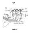
- FIG. 7is a plan view showing a multi-connector provided at one end of a wiring trace, in which (A) is a plan view of a soldering iron contacting side and (B) is a plan view of a side for contact with a flexible printed circuit board.
- a wiring trace 500 used in the second methodcomprises an insulating layer 502 , four conductor patterns 503 a , 503 b , 503 c , and 503 d , and a cover layer 504 .
- the four conductor patternsare arranged side by side on a surface of the insulating layer 502 .
- the cover layer 504is formed on surfaces of the conductor patterns 503 a , 503 b , 503 c , 503 d and the surface of the insulating layer 502 so as to cover the conductor patterns 503 a , 503 b , 503 c , and 503 d .
- the wiring trace 500is provided at one end thereof with a multi-connector 501 .
- the multi-connector 501is provided with four terminals 505 a , 505 b , 505 c , and 505 d at equal intervals in a longitudinal direction of the conductor patterns 503 a , 503 b , 503 c , and 503 d .
- the terminals 505 a , 505 b , 505 c , and 505 dare portions of the conductor patterns 503 a , 503 b , 503 c , and 503 d , respectively, and are formed as somewhat wide patterns at front ends of the conductor patterns.
- a single rectangular aperture 506In the insulating layer 502 of the multi-connector 501 is formed a single rectangular aperture 506 so that the four terminals 505 a , 505 b , 505 c , and 505 d are partially exposed from the aperture.
- a cover layer 504 a of the multi-connector 501is formed separately from the cover layer 504 of the wiring trace 500 .
- a single rectangular aperture 507is formed in the cover layer 504 a so that the four terminals 505 a , 505 b , 505 c , and 505 d are partially exposed from the aperture.
- FIG. 8is an explanatory diagram showing a connection structure in which the terminals 505 a , 505 b , 505 c , and 505 d of the multi-connector 501 are soldered onto terminals 602 a , 602 b , 602 c , and 602 d of a flexible printed circuit board 600 .
- the terminals 602 a , 602 b , 602 c , and 602 dare provided on end sides of conductor patterns 601 a , 601 b , 601 c , and 601 d serving as four lead wires.
- the multi-connector 501is bent from the wiring trace 500 so that the aperture 506 of the insulating layer 502 (see FIG.
- the conductor patterns 601 a , 601 b , 601 c , and 601 d of the flexible printed circuit board 600are represented by solid lines except the portion covered with the multi-connector 501 .
- the terminals 505 a , 505 b , 505 c , and 505 d of the multi-connector 501 thus placed on the flexible printed circuit board 600are aligned onto the terminals 602 a , 602 b , 602 c , and 602 d of the same printed circuit board and are then heated with a soldering iron.
- solder bumps formed on the terminals 602 a , 602 b , 602 c , and 602 dmelt, so that the terminals 505 a , 505 b , 505 c , 505 d and the terminals 602 a , 602 b , 602 c , 602 d , which are exposed from the aperture 506 of the insulating layer 502 , are connected together by solder 508 so as to be covered substantially throughout the whole surface. All that is required for this soldering work is a mere fixing of the head suspension assembly to a jig. Thus, mass production can be effected even by manual operation, and therefore the device cost can be kept to a minimum.
- the terminals 505 a , 505 b , 505 c , and 505 d of the multi-connector 501are in an uncovered state (flying leads) over the space within the aperture 506 formed in the insulating layer 502 and also over the space within the aperture 507 formed in the cover layer 504 .
- solder bumpsare formed on the terminals 602 a , 602 b , 602 c , and 602 d of the flexible printed circuit board 600 , then the terminals 505 a , 505 b , 505 c , and 505 d of the multi-connector 501 are aligned onto the solder bumps.
- the terminals 505 a , 505 b , 505 c , and 505 d of the multi-connector 501are heated with a soldering iron to melt the solder bumps and effect soldering thereby.
- the connection structure shown in FIG. 8however, with only the solder 508 formed by melting the solder bumps, there sometimes occurs a case where the strength is low.
- the terminals of the multi-connector 501are in an uncovered state (flying leads) over the space within the aperture 506 formed in the insulating layer 502 and also over the space within the aperture 507 formed in the cover layer 504 a.
- solderingis performed so as to cover the whole of the terminals of the multi-connector 501 from above the terminals with solder, not only is it necessary to use solder other than the solder bumps, but also flux caused by contamination increases.
- the present inventionhas been accomplished for solving the above-mentioned conventional problems. It is a feature of the present invention to provide a highly reliable terminal structure and wiring connection structure able to improve productivity. It is another feature of the present invention to prevent cracking of terminals of a wiring trace in a head suspension assembly at the time of connecting terminals of a flexible printed circuit board with the terminals of the wiring trace and also prevent the addition of solder. It is yet another feature of the present invention to provide a magnetic disk drive using those terminal structure and wiring connection structure.
- a terminal structure formed in a wiring traceincluding an insulating layer and a conductor pattern formed on a surface of the insulating layer.
- the conductor patterncomprises an exposed portion exposed from an aperture formed in part of the insulating layer and a lining portion adjacent to the exposed portion in a longitudinal direction of the conductor pattern and bonded to the insulating layer.
- a wiring connection structureconnecting a flexible printed circuit board and a wiring trace with each other, the flexible printed circuit board including terminals, the wiring trace including an insulating layer and a conductor pattern formed on a surface of the insulating layer.
- the conductor patternincludes an exposed portion exposed from an aperture formed in part of the insulating layer and a lining portion bonded to the insulating layer in adjacency to the exposed portion in a longitudinal direction of the conductor pattern.
- the terminals of the flexible printed circuit board and the exposed portion of the conductor patternare soldered to each other.
- a magnetic disk drivecomprising a magnetic disk, a head for reading data from the magnetic disk, and an actuator head suspension assembly with the head attached thereto.
- the magnetic disk drivecomprises a wiring trace including an insulating layer and a conductor pattern formed on a surface of the insulating layer and connected to the head.
- the conductor patternincludes an exposed portion exposed from an aperture formed in part of the insulating layer and a lining portion adjacent to the exposed portion in a longitudinal direction of the conductor pattern and bonded to the insulating layer.
- the magnetic disk drivestill further comprises a flexible printed circuit board connected to the wiring trace.
- the present inventionis an improved invention of a terminal structure and a wiring connection structure in connection with terminals formed in a wiring trace and connected to terminals of a flexible printed circuit board.
- a terminal formed in a conductor pattern of the wiring traceis provided with an exposed portion exposed from an aperture formed in part of an insulating layer and a lining portion adjacent to the exposed portion in a longitudinal direction of the conductor pattern and bonded to the insulating layer.
- the exposed portionis strengthened and difficult to be cracked. Even if the exposed portion should be cracked, there is no fear that the crack may reach the lining portion. Thus, the conductivity of the terminal is ensured. If a through aperture extending through an area of the insulating layer adjacent to the exposed portion in the longitudinal direction of the conductor pattern is formed in the aperture formed in part of the insulating layer, solder comes to connect a heating surface and a contact surface of the exposed portion with each other through the through aperture. Once the solder thus connects the heating surface and the contact surface of the exposed portion with each other through the through area of the insulating layer, the solder connection by the lapping of solder becomes stronger.
- the “lining portion adjacent to the exposed portion and bonded to the insulating layer” as referred to hereinmeans that the exposed portion and the lining portion are in contact with each other adjacently and continuously.
- the conductor patternincludes a first conductor pattern provided with the exposed portion and the lining portion and a second conductor pattern also provided with the exposed portion and the lining portion, and the portions of the insulating layer corresponding to the lining portion of the first conductor pattern and the lining portion of the second conductor pattern are connected together on an end side of the wiring trace rather than the lining portions.
- the aspect just described aboveis concerned with conductor patterns having plural terminals, and since the portions of the insulating layer corresponding to the lining portions of the first and second conductor patterns are connected together at a foremost end portion of the wiring trace rather than the lining portions, the strength of the insulating layer may be enhanced around the aperture.
- the present inventionit is possible to provide a magnetic disk drive able to connect terminals of a flexible printed circuit board and terminals of a wiring trace in a head suspension assembly with each other by soldering without giving rise to any soldering defect, as well as a wiring connection structure and a terminal structure both used in the magnetic disk drive. According to the present invention, moreover, it is possible to provide a magnetic disk drive able to improve productivity and superior in soldering function, as well as a wiring connection structure and a terminal structure both used therein.
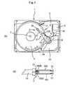
- FIG. 1shows a magnetic disk drive according to an embodiment of the present invention, in which (A) is a plan view and (B) is a side view of an actuator head suspension assembly.
- FIG. 2is a perspective view for explaining the construction of an HGA according to the embodiment.
- FIG. 3is a plan view for explaining the structure of a gimbal assembly in a wiring trace according to the embodiment.
- FIG. 4is a plan view for explaining the structure of a multi-connector in the wiring trace according to the embodiment.
- FIG. 5is a plan view showing a wiring connection structure and a terminal structure of the multi-connector according to the embodiment.
- FIG. 6is a plan view for explaining a wiring connection structure and a terminal structure of a multi-connector according to another embodiment of the present invention.
- FIG. 7is a plan view showing a terminal structure of a conventional multi-connector.
- FIG. 8is a plan view showing a wiring connection structure and the terminal structure of the conventional multi-connector.
- FIG. 1illustrates a magnetic disk drive 1 according to an embodiment of the present invention, in which (A) is a plan view showing a schematic construction of the magnetic disk drive and (B) is a partially enlarged side view of an actuator head suspension assembly as seen in the direction of arrow A′ in (A).
- a base 2together with a base cover (not shown), forms a hermetically sealed space.
- An actuator head suspension assembly 3 , a magnetic disk 4 , a ramp 5 , and an external terminal 6 to be connected to a circuit board,are accommodated within the hermetically sealed space.
- the magnetic disk 4is fixed to a spindle hub (not shown) so as to be rotated around a spindle shaft 7 by a spindle motor (not shown) disposed at a lower position.
- a magnetic layeris formed on at least one surface of the magnetic disk 4 .
- Two or more magnetic disks 4may be stacked.
- a rotational direction of arrow A of the magnetic disk 4is designated a forward rotation
- a rotational direction of arrow B of the diskis designated a reverse rotation, in relation to the actuator head suspension assembly 3 .
- the difference between the forward rotation and the reverse rotationappears mainly in the position of a head on a slider.
- the present inventionis applicable to magnetic disk drives of both forward and reverse rotation types.
- the actuator head suspension assembly 3comprises an actuator assembly 31 and a head gimbal assembly (hereinafter referred to as “HGA”) 32 so as to be pivotable about a pivot shaft 8 .
- HGAhead gimbal assembly
- two HGAs 32are provided in a sandwiching relation to the magnetic disk 4 so that read and write of data may be done for both surfaces of the magnetic disk 4 .
- the actuator assembly 31comprises actuator arms 33 for mounting the HGAs 32 , a coil support 34 for holding a voice coil (not shown), and a pivot housing which corresponds to a connection between the actuator arms 33 and the coil support 34 .
- a voice coil yoke 35is provided on the base 2 , and a voice coil magnet (not shown), which is a permanent magnet, is attached to a back side of the voice coil yoke 35 .
- the HGAs 32each comprise a load beam and a gimbal assembly which will be described in detail later.
- a merged lip 36is formed at a front end of the load beam, and there is realized a so-called load/unload method wherein the merged lip 36 is allowed to slide on a retraction surface of the ramp 5 before stop of rotation of the magnetic disk 4 and the head/slider is retracted from above the surface of the magnetic disk 4 .
- the application of the present inventionis not limited to the magnetic disk drive of the load/unload type, but the present invention is also applicable to a magnetic disk drive of a contact start/stop type.
- the merged lips 36 , HGAs 32 and actuator arms 33are formed as a stack structure in a corresponding relation to the recording surfaces of the magnetic disk 4 .
- a relay terminal portion 37is provided in the actuator assembly 31 to provide connection between a wiring trace 100 connected to the head and a flexible printed circuit board 10 connected to the external terminal 6 . The details of the wiring trace 100 and the flexible printed circuit board 10 will be described later.
- FIG. 2is an exploded perspective view illustrating the construction of each HGA 32 .
- Each HGA 32comprises a mounting plate 321 , two pieces of load beams 322 a and 322 b , a hinge 323 , and a gimbal assembly 100 A.
- the load beamsneed not always be two-piece load beams. A one-piece load beam will do.
- the gimbal assembly 100 Ais provided at one end of the wiring trace 100 and adopts a wiring integrated type suspension structure as will be described later.
- the head/slider, indicated at 102is attached to a flexure tongue or gimbal tongue (see the reference numeral 103 in FIG. 3 ) of the gimbal assembly 100 A on the side confronting a recording surface of the magnetic disk 4 .
- the load beams 322 a and 322 bare fixed with a hinge 323 and the mounting plate 321 is fixed integrally by spot welding or by use of an adhesive.
- the mounting plate 321is swaged to fix the HGA 32 to the actuator arm 33 .
- the load beams 322 a and 322 bpivot together with the actuator assembly 31 to carry the head/slider 102 up to a predetermined track and provide a pushing load for pushing the head/slider 102 against the opposed surface of the magnetic disk 4 .
- the head/slider 102flies through a predetermined spacing from the surface of the rotating magnetic disk 4 .
- the gimbal assembly side as one endis connected (not shown) through a wiring pad to a slider pad formed on the head slider.
- the opposite endis connected through a multi-connector 100 B to the flexible printed circuit board 10 , as shown in FIG. 1(B) .
- the wiring trace 100 having the gimbal assembly 100 A and the multi-connector 100 Bis of a construction wherein a conductor layer which constitutes a conductor pattern and an insulating layer which insulates the conductor layer are stacked one on the other.
- a cover layer as a dielectric for the prevention of corrosionis formed on the conductor layer to sandwich the conductor layer in between insulating layers.
- a metal layer as a structure for supporting the head/slider 102is formed on an insulating layer.
- the wiring trace 100 having such a stack structurethere are three types which are an additive type, a subtractive type, and a flexible board type, according to different manufacturing methods.
- the additive typeis a method in which various layers are stacked in order in accordance with the photolithography technique.
- the subtractive typeis a method in which a sheet pre-formed with metal layer, insulating layer, conductor layer, and cover layer, is etched to form a predetermined structure.
- the flexible board typeis a method in which a flexible printed circuit board formed in a predetermined shape by insulating layer, conductor layer, and cover layer, is affixed onto a metal layer.
- the wiring trace 100 used in this embodimentis the flexible board type, but the gimbal assembly 100 A is the additive type.
- FIG. 3illustrates a stack structure of the gimbal assembly 100 which is a wiring integrated type suspension of the wiring trace 100 .
- the gimbal assembly 100 Ais formed by using a semiconductor processing technique such as a photolithographic etching process or a vapor deposition process.
- FIG. 3(A)shows the gimbal assembly 100 A completed by stacking plural layers, and the structures of the constituent layers of the gimbal assembly 100 A are shown in FIGS. 3(B) to 3(E) .
- FIG. 3(A)shows the completed gimbal assembly 100 A as seen from the magnetic disk 4 side, in which the head/slider 102 is omitted for simplification of the drawing.
- FIGS. 3(B) to 3(E)are drawn in the order of stacking toward the magnetic disk surface.
- FIG. 3(B)shows a plane of a metal layer 111 A, in which as the material of the metal layer there is selected SUS 304 having a sheet thickness of 0.02 mm from among 300 Series stainless steels.
- the material of the metal layer 111 Ais not limited to stainless steel, but there also may be selected another hard spring material such as beryllium, copper, or titanium.
- the metal layer 111 Aincludes a gimbal tongue 103 .
- FIG. 3(C)shows a plane of an insulating layer 113 A which is formed of a polyimide or epoxy resin for insulating the metal layer 111 A and conductor layer 115 A.
- the insulating layer 113 Ais formed on the metal layer 111 A in a shape conforming to the pattern of the conductor layer 115 A. In this embodiment, the thickness of the insulating layer is set to 0.01 mm. Part of the insulating layer 113 A is formed also on the gimbal tongue 103 .
- FIG. 3(D)shows the conductor layer 115 A which is a wiring pattern for the head.
- patterningis made by stacking pure copper to a thickness of 0.012 mm.
- the material of the conductor layeris not limited to copper, but may be another material such as aluminum or silver.
- FIG. 3(E)shows a pattern of a cover layer 117 A which is for protecting a surface of the conductor layer 115 A.
- the cover layer 117 Ais formed by adhering a polyimide or epoxy layer of about 0.003 mm in thickness onto the conductor layer 115 A.
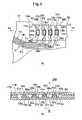
- FIG. 4shows a stack structure of the multi-connector 100 B of the wiring trace 100 .
- the multi-connector 100 Bis formed by a semiconductor processing technique such as a photolithographic etching process or a vapor deposition process.
- the multi-connector 100 B completed by stacking plural layersis shown in FIG. 4(A) and structures of constituent layers of the multi-connector 100 B are shown in FIGS. 4(B) to 4(D) .
- FIG. 4(A)shows the completed multi-connector 100 B as seen from the flexible printed circuit board 10 side.
- FIGS. 4(B) to 4(D)are drawn in the order of stacking the constituent layers toward the flexible printed circuit board.
- FIG. 4(B)shows a plane of the insulating layer 113 B formed using a polyimide or epoxy resin for example.
- the insulating layer 113 Bis formed in a shape conforming to the pattern of the conductor layer 115 B.
- the conductor layer 115 Bis stacked on the insulating layer 113 B.
- the thickness of the insulating layeris set at 0.01 mm.
- FIG. 4(C)shows the conductor layer 115 B which is a wiring pattern including terminals.
- patterningis made by stacking pure copper to a thickness of 0.012 mm.
- the material of the conductor layeris not limited to copper, but may be another material such as aluminum or silver.
- FIG. 4(D)shows a pattern of a cover layer 117 B for protecting a surface of a conductor layer 115 B.
- the cover layer 117 Bis formed by adhering a polyimide or epoxy layer of about 0.003 mm in thickness onto the conductor layer 115 B.
- the thicknesses of the insulating layer 113 B, conductor layer 115 B and cover layer 117 B, as well as the metal layer 111 A, insulating layer 113 A, conductor layer 115 A, and cover layer 117 Aare illustrative and the scope of the present invention is not limited thereto.
- the conductor layer 115 Bis divided into two pairs, constituting a total of four conductor patterns 120 a , 120 b , 120 c , and 120 d as four lead wires.
- the conductor patterns 120 a , 120 b , 120 c , and 120 dthere are formed terminals 121 a , 121 b , 121 c , and 121 d , respectively, in a longitudinal direction of those conductor patterns.
- the terminals 121 a , 121 b , 121 c , and 121 dare formed in a rectangular shape and are spaced at equal intervals so that their short sides are aligned with one another.
- the terminals 121 a , 121 b , 121 c , and 121 d of the conductor patterns 120 a , 120 b , 120 c , and 120 d in the conductor layer 115 Bare respectively provided with exposed portions 131 a , 131 b , 131 c , and 131 d exposed from the apertures 122 a , 122 b , 122 c , and 122 d in the insulating layer 113 B and also provided with lining portions 132 a , 132 b , 132 c , and 132 d adjacent to the exposed portions 131 a , 131 b , 131 c , and 131 d and bonded to the insulating layer 113 B.
- the lining portions 132 a , 132 b , 132 c , and 132 dare areas bonded to the insulating layer 113 B and exhibiting an action of strengthening the terminals 121 a , 121 b , 121 c , and 121 d , the larger the area thereof, the better.
- the exposed potions 131 a , 131 b , 131 c , and 131 dthe larger the area thereof the easier the work, because they are areas to be heated with a soldering iron.
- each of the terminals 121 a , 121 b , 121 c , and 121 dcomprising the lining portions 132 a , 132 b , 132 c , 132 d and the exposed portions 131 a , 131 b , 131 c , 131 d be set within a certain range, taking into account the necessity of ensuring a certain space between adjacent terminals and restrictions on the whole area of the multi-connector 100 B.
- the area of the lining portions 132 a , 132 b , 132 c , and 132 d relative to the total area of the area of the exposed portions 131 a , 131 b , 131 c , 131 d and the lining portions 132 a , 132 b , 132 c , 132 dis set in the range of 30% to 70%, preferably 40% to 60%, then the area which the exposed portions 131 a , 131 b , 131 c , and 131 d require for appropriate soldering and the area which the lining portions 132 a , 132 b , 132 c , and 132 d require for strengthening the terminal structure, may be set in a well-balanced manner.
- the exposed portions 131 a , 131 b , 131 c , and 131 dmay be provided throughout the whole of the apertures 122 a , 122 b , 122 c , and 122 d . However, if the exposed portions 131 a , 131 b , 131 c , and 131 d are provided so as to occupy only part of the areas of the apertures 122 a , 122 b , 122 c , and 122 d and allow through apertures to remain in the apertures 122 a , 122 b , 122 c , and 122 d , it becomes easier to make a visual alignment at the time of connecting the terminals of the flexible printed circuit board 10 and the terminals 121 a , 121 b , 121 c , 121 d , of the conductor patterns 120 a , 120 b , 120 c , 120 d , and solder may be allowed to reach back surfaces from
- the areas of the exposed portions 131 a , 131 b , 131 c , and 131 d corresponding to surfaces of the terminals 121 a , 121 b , 121 c , and 121 dwill hereinafter be referred to as “heating surfaces” and the areas of the exposed portions 131 a , 131 b , 131 c , 131 d and of the lining portions 132 a , 132 b , 132 c , 132 d corresponding to back surfaces of the terminals 121 a , 121 b , 121 c , 121 d will hereinafter be referred to as “contact surfaces.”
- a single rectangular aperture 123is formed in a cover layer 117 B′ of the multi-connector 100 B in such a manner that the terminals 121 a , 121 b , 121 c , and 121 d of the conductor patterns 120 a , 120 b , 120 c , and 120 d are exposed except both of their longitudinal end portions.
- the cover layer 117 B′ of the multi-connector 100 B and the cover layer 117 B of the wiring trace 100are separated in two from each other, centered on a bent portion 124 .
- the bent portion 124is provided in the insulating layer 113 B.
- Three small apertures 125 a , 125 b , and 125 care formed in the insulating layer 113 B along the long sides of the aperture 123 formed in the cover layer 117 B in order to make the multi-connector 100 B and the wiring trace 100 easier to be bent along a side face of the flexible printed circuit board 10 at the relay terminal portion 37 .
- By bending the flexible printed circuit board and the wiring trace along the apertures 125 a , 125 b , and 125 cit becomes easier to align and fix the terminals 121 a , 121 b , 121 c , and 121 d of the multi-connector 100 B onto terminals 12 a , 12 b , 12 c , and 12 d (see FIG. 5 ) of the flexible printed circuit board 10 at the relay terminal portion 37 .
- the wiring trace 100is not always required to have the cover layer 117 B.
- the aperture 123is formed as a single aperture. This is for close contact between the terminals 12 a , 12 b , 12 c , 12 d of the flexible printed circuit board 10 and the contact surfaces of the terminals 121 a , 121 b , 121 c , 121 d of the multi-connector 100 B.
- FIG. 5illustrates the wiring connection structure according to the present invention shown in FIG. 1(B) , in which (A) is an enlarged plan view and (B) is a sectional view taken on line A-A in (A).
- a conductor layer 11which is insulated sandwichingly by flexible sheets, is divided into pairs each for a single head.
- the conductor layer 11is composed of conductor patterns 11 a , 11 b , 11 c , and 11 d serving as four lead wires as a whole.
- conductor patternsare formed by the number corresponding to the number of heads.
- Terminals 12 a , 12 b , 12 c , and 12 dwhich are exposed in a longitudinal direction of the conductor patterns 11 a , 11 b , 11 c , and 11 d , are formed at end portions of those conductor patterns on the side to be soldered to the contact surfaces of the terminals 121 a , 121 b , 121 c , and 121 d of the multi-connector 100 B.
- the terminals 12 a , 12 b , 12 c , and 12 dare formed in a rectangular shape and are spaced at equal intervals so that their short sides are aligned with one another.
- Solder bumpsare formed on the terminals 12 a , 12 b , 12 c , and 12 d of the flexible printed circuit board 10 .
- the conductor patterns 11 a , 11 b , 11 c , and 11 d of the flexible printed circuit board 10are indicated by broken lines at their portions covered with the multi-connector 100 B and by solid lines at their uncovered portions.
- the terminals 121 a , 121 b , 121 c , and 121 d of the multi-connector 100 Bthus constructed and the terminals 12 a , 12 b , 12 c , and 12 d of the flexible printed circuit board 10 are soldered together at the relay terminal portion 37 of the actuator assembly 31 . This soldering step will be described below with reference to FIGS. 4 and 5 .
- the actuator head suspension assembly 3which is assembled in advance, is installed in a working jig (not shown) in such a manner that the relay terminal portion 37 faces up.
- the portion of the flexible printed circuit board 10 where the terminals 12 a , 12 b , 12 c , and 12 d are formedis bonded to the relay terminal portion 37 with use of, for example, a thermosetting adhesive.
- a thermosetting adhesivefor example, an epoxy resin is used as the thermosetting adhesive.
- the wiring trace 100 with the terminals on the gimbal assembly 100 A side soldered beforehand to the head/slider 102 of the HGA 32is disposed along the actuator arm 33 . In this state, the wiring trace 100 is hooked to a hook portion (not shown) provided near the relay terminal portion 37 of the actuator arm 33 .
- the wiring trace 100 and the multi-connector 100 Bare bent along the bent portion 124 . More particularly, the cover layer 117 B side is bent in a valley shape so that the cover layer 117 B side of the multi-connector 100 B confronts the terminals 12 a , 12 b , 12 c , and 12 d of the flexible printed circuit board 10 .
- the terminals 121 a , 121 b , 121 c , and 121 d of the multi-connector 100 Bare aligned onto the terminals 12 a , 12 b , 12 c , and 12 d of the flexible printed circuit board 10 with use of a tool such as tweezers, and the terminals 121 a , 121 b , 121 c , and 121 d are soldered in this order.
- the cover layer 117 Bis positioned between the terminals 12 a , 12 b , 12 c and 12 d and the terminals 121 a , 121 b , 121 c , and 121 d to form a gap therebetween.
- the cover layer 117 Bis about 0.003 mm in thickness and not separated plural apertures, but a single large aperture 123 is formed, the contact surfaces of the terminals may come into close contact with the terminals of the flexible printed circuit board 10 .
- This soldering stepis carried out in the following manner.
- the heating surfaces of the terminal exposed portions 131 a , 131 b , 131 c , and 131 dare heated with a soldering iron (not shown) to melt the solder bumps on the terminals of the flexible printed circuit board 10 .
- solders 200 a , 200 b , 200 c , and 200 dconnect the heating surfaces and the contact surfaces of the exposed portions 131 a , 131 b , 131 c , and 131 d with each other through the through apertures, as shown in FIG. 5 .
- solders 200 a , 200 b , 200 c , and 200 dthus connect the heating surfaces and the contact surfaces of the exposed portions 131 a , 131 b , 131 c , and 131 d with each other through the through area of the insulating layer 113 B, not only the soldered connections are made strong but also the strength of the terminals is enhanced by lapping of the solders 200 a , 200 b , 200 c , and 200 d.
- the terminals of the multi-connector 100 Bmay be cracked because they are very thin (e.g., 0.012 mm).
- the terminals of the multi-connector 100 Bare partially bonded as lining portions 132 a , 132 b , 132 c , and 132 d to the insulating layer 113 B and it is only the exposed portions 131 a , 131 b , 131 c , and 131 d that are uncovered (flying leads) over the spaces of the apertures formed in the insulating layer 113 B. Therefore, at edges of the apertures, the exposed portions are difficult to be cracked and thus it is possible to strengthen the terminals. Even if the exposed portions are cracked, the cracks do not reach the lining portions 132 a , 132 b , 132 c , and 132 d and hence conductivity is ensured. If such a terminal structure is adopted, it becomes no longer necessary to use a preliminary solder so far provided on heating surfaces for lapping of solder between the heating surfaces and contract surfaces in order to strengthen the terminal structure.
- the insulating layer 113 Bconnects at the foremost end of the multi-connector 100 B rather than the lining portions 132 a , 132 b , 132 c , and 132 d .
- the strength of the insulating layer 113 Bmay be enhanced around the apertures 122 a , 122 b , 122 c , and 122 d , and it is possible to strengthen the terminals 121 a , 121 b , 121 c , and 121 d.
- the terminals 121 a , 121 b , 121 c , and 121 d of the conductor patterns 120 a , 120 b , 120 c , and 120 dare 0.35 mm in width and 1.4 mm in length.
- the apertures 122 a , 122 b , 122 c , and 122 d formed in the insulating layer 113 B of the multi-connector 100 Bare 0.5 mm wide and 0.7 mm long.
- the width of each of the apertures 122 a , 122 b , 122 c , and 122 d formed through the area of the insulating layer 113 B adjacent to the exposed portions 131 a , 131 b , 131 c , and 131 dis set at 0.3 mm.
- the lining portions 132 a , 132 b , 132 c , and 132 dare provided on one sides of the exposed portions 131 a , 131 b , 131 c , and 131 d .
- lining portionsmay be provided on both sides of the exposed portions 131 a , 131 b , 131 c , and 131 d.
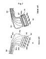
- FIG. 6shows another embodiment of the present invention in connection with the exposed portions 131 a , 131 b , 131 c , 131 d and the lining portions 132 a , 132 b , 132 c , 132 d in the multi-connector 100 B. As shown in FIG.
- Such through apertures 133 a , 133 b , 133 c , and 133 d as shown in FIG. 6(B)may be formed in the exposed portions 131 a , 131 b , 131 c , and 131 d with lining portions 132 a , 132 b , 132 c , and 132 d formed on both sides thereof.
- solder used in solderingmay connect the heating surfaces and the contact surfaces of the exposed portions 131 a , 131 b , 131 c , and 131 d with each other and thus the solder connection becomes stronger.
- the through apertures 133 a , 133 b , 133 c , and 133 dmay take any of various shapes including circular and quadrangular shapes insofar as the solder may connect the heating surfaces and the contact surfaces of the exposed portions 131 a , 131 b , 131 c , and 131 d with each other through the through apertures 133 a , 133 b , 133 c , and 133 d.
- the heating surfaces of the exposed portions 131 a , 131 b , 131 c , and 131 d of the exposed portionsare heated with a soldering iron to melt the solder bumps on the terminals of the flexible printed circuit board 10 , thereby soldering the multi-connector 100 B and the flexible printed circuit 10 with each other, this constitutes no limitation and thread-like solder or the like may be used. In this case, thread-like solder is melted and placed onto the exposed portions 131 a , 131 b , 131 c , and 131 d .
- the solder used in solderingmay connect the heating surfaces and the contact surfaces of the exposed portions 131 a , 131 b , 131 c , and 131 d with each other. Even if such through apertures 133 a , 133 b , 133 c , and 133 d as shown in FIG.
- solder used in solderingmay connect the heating surfaces and the contact surfaces of the exposed portions 131 a , 131 b , 131 c , and 131 d with each other.
- terminals of conductor patterns and the apertures of the insulating layer 113 B and of the cover layer 117 B in the multi-connector 100 Bare all formed rectangularly, no limitation is made thereto and they may be in any other shape insofar as the exposed portions are exposed from the apertures of the insulating layer 113 B, the lining portions are bonded to the insulating layer 113 B and the terminals of the multi-connector 100 B and the terminals of the flexible printed circuit board 10 may be soldered to each other.
- the multi-connector 100 Bis provided at an end of the wiring trace 100 , no limitation is made thereto, and the multi-connector 100 B may be provided at a certain intermediate position of the wiring trace 100 .
- the terminals of the multi-connector 100 B and the terminals of the flexible printed circuit board 10are soldered to each other, no limitation is made thereto and both may be connected by ultrasonic bonding.
- ultrasonic bondingthere is used a bonding tool which comes into contact with an object to be bonded and which imparts an ultrasonic oscillation to the object. More specifically, the tip of a bonding tool used in place of the soldering iron is put in contact with a terminal of the multi-connector 100 B which is superimposed on a terminal of the flexible printed circuit board 10 , under a predetermined pressure, and produces an ultrasonic oscillation between both terminals.
Landscapes
- Engineering & Computer Science (AREA)
- Manufacturing & Machinery (AREA)
- Microelectronics & Electronic Packaging (AREA)
- Coupling Device And Connection With Printed Circuit (AREA)
- Adjustment Of The Magnetic Head Position Track Following On Tapes (AREA)
- Supporting Of Heads In Record-Carrier Devices (AREA)
- Insulated Metal Substrates For Printed Circuits (AREA)
- Printing Elements For Providing Electric Connections Between Printed Circuits (AREA)
- Combinations Of Printed Boards (AREA)
Abstract
Description
Claims (4)
Priority Applications (1)
| Application Number | Priority Date | Filing Date | Title |
|---|---|---|---|
| US12/079,700US7724478B2 (en) | 2004-08-09 | 2008-03-27 | Magnetic disk drive, wiring connection structure and terminal structure |
Applications Claiming Priority (2)
| Application Number | Priority Date | Filing Date | Title |
|---|---|---|---|
| JP2004-231948 | 2004-08-09 | ||
| JP2004231948AJP2006049751A (en) | 2004-08-09 | 2004-08-09 | Magnetic disk drive, wiring connection structure and terminal structure thereof |
Related Child Applications (1)
| Application Number | Title | Priority Date | Filing Date |
|---|---|---|---|
| US12/079,700DivisionUS7724478B2 (en) | 2004-08-09 | 2008-03-27 | Magnetic disk drive, wiring connection structure and terminal structure |
Publications (2)
| Publication Number | Publication Date |
|---|---|
| US20060034018A1 US20060034018A1 (en) | 2006-02-16 |
| US7372669B2true US7372669B2 (en) | 2008-05-13 |
Family
ID=35799711
Family Applications (2)
| Application Number | Title | Priority Date | Filing Date |
|---|---|---|---|
| US11/200,865Expired - Fee RelatedUS7372669B2 (en) | 2004-08-09 | 2005-08-09 | Magnetic disk drive, wiring connection structure and terminal structure |
| US12/079,700Expired - LifetimeUS7724478B2 (en) | 2004-08-09 | 2008-03-27 | Magnetic disk drive, wiring connection structure and terminal structure |
Family Applications After (1)
| Application Number | Title | Priority Date | Filing Date |
|---|---|---|---|
| US12/079,700Expired - LifetimeUS7724478B2 (en) | 2004-08-09 | 2008-03-27 | Magnetic disk drive, wiring connection structure and terminal structure |
Country Status (2)
| Country | Link |
|---|---|
| US (2) | US7372669B2 (en) |
| JP (1) | JP2006049751A (en) |
Cited By (28)
| Publication number | Priority date | Publication date | Assignee | Title |
|---|---|---|---|---|
| US20060158785A1 (en)* | 2005-01-18 | 2006-07-20 | Arya Satya P | Electrical lead suspension having partitioned air slots |
| US20070295534A1 (en)* | 2006-06-22 | 2007-12-27 | Nitto Denko Corporation | Wired circuit board |
| US20080151432A1 (en)* | 2006-12-20 | 2008-06-26 | Toshiki Hirano | High frequency interconnect signal transmission lines |
| US20090219652A1 (en)* | 2005-05-04 | 2009-09-03 | Michael Bammert | Actuator for access to strorage media |
| US20090268417A1 (en)* | 2007-03-13 | 2009-10-29 | Fujitsu Limited | Storage apparatus and printed wiring board unit |
| US20100155457A1 (en)* | 2008-12-23 | 2010-06-24 | Edgar Rothenberg | Reducing a generation of contaminants during a solder reflow process |
| US20100220414A1 (en)* | 2009-03-02 | 2010-09-02 | Seagate Technology Llc | Head gimbal assembly without bus traces for plating |
| US20100290160A1 (en)* | 2009-05-15 | 2010-11-18 | Nhk Spring Co., Ltd. | Disk drive flexure |
| US20120134047A1 (en)* | 2010-11-30 | 2012-05-31 | Kabushiki Kaisha Toshiba | Head gimbal assembly and disk drive with the same |
| US8295013B1 (en) | 2010-10-29 | 2012-10-23 | Western Digital Technologies, Inc. | Disk drive head stack assembly having a flexible printed circuit with heat transfer limiting features |
| US8295014B1 (en) | 2010-10-29 | 2012-10-23 | Western Digital Technologies, Inc. | Disk drive head gimbal assembly having a flexure tail with transverse flying leads |
| US8320084B1 (en) | 2010-10-29 | 2012-11-27 | Western Digital Technologies, Inc. | Disk drive head gimbal assembly having a flexure tail with features to facilitate bonding |
| US8320083B1 (en)* | 2007-12-06 | 2012-11-27 | Magnecomp Corporation | Electrical interconnect with improved corrosion resistance for a disk drive head suspension |
| US8325446B1 (en) | 2010-10-29 | 2012-12-04 | Western Digital Technologies, Inc. | Disk drive head gimbal assembly having a flexure tail with features to facilitate bonding |
| US8467153B1 (en) | 2010-10-29 | 2013-06-18 | Western Digital Technologies, Inc. | Disk drive head gimbal assembly having a flexure tail with folded bond pads |
| US8477459B1 (en) | 2010-10-29 | 2013-07-02 | Western Digital Technologies, Inc. | Disk drive head gimbal assembly having a flexure tail with dual conductive layers and features to facilitate bonding |
| US8665566B1 (en) | 2011-12-20 | 2014-03-04 | Western Digital Technologies, Inc. | Suspension tail design for a head gimbal assembly of a hard disk drive |
| US8760812B1 (en) | 2011-12-20 | 2014-06-24 | Western Digital Technologies, Inc. | Disk drive head gimbal assembly having a jumper in a flexible printed circuit overlap region |
| US8934199B1 (en) | 2014-03-31 | 2015-01-13 | Western Digital Technologies, Inc. | Disk drive head suspension tail with bond pad edge alignment features |
| US8934201B1 (en)* | 2013-12-09 | 2015-01-13 | Sae Magnetics (H.K.) Ltd. | Flexure, head gimbal assembly and disk drive unit with the same |
| US20150124352A1 (en)* | 2013-11-04 | 2015-05-07 | HGST Netherlands B.V. | Flexible cable assembly having reduced-tolerance electrical connection pads |
| US9165580B2 (en) | 2013-12-10 | 2015-10-20 | Western Digital Technologies, Inc. | Disk drive head suspension tail with stiffened edge alignment features |
| US9274978B2 (en) | 2013-06-10 | 2016-03-01 | Western Digital Technologies, Inc. | Migration of encrypted data for data storage systems |
| US9324344B1 (en) | 2013-12-10 | 2016-04-26 | Western Digital Technologies, Inc. | Disk drive head suspension tail with ground pad outside of bonding region |
| US9330695B1 (en) | 2013-12-10 | 2016-05-03 | Western Digital Technologies, Inc. | Disk drive head suspension tail with a noble metal layer disposed on a plurality of structural backing islands |
| US9335950B2 (en) | 2013-03-15 | 2016-05-10 | Western Digital Technologies, Inc. | Multiple stream compression and formatting of data for data storage systems |
| US9448738B2 (en) | 2013-03-15 | 2016-09-20 | Western Digital Technologies, Inc. | Compression and formatting of data for data storage systems |
| US9633680B2 (en) | 2010-10-29 | 2017-04-25 | Western Digital Technologies, Inc. | Head suspension having a flexure tail with a covered conductive layer and structural layer bond pads |
Families Citing this family (40)
| Publication number | Priority date | Publication date | Assignee | Title |
|---|---|---|---|---|
| US7646567B2 (en)* | 2005-06-28 | 2010-01-12 | Seagate Technology Llc | Flex on suspension with a heat-conducting protective layer for reflowing solder interconnects |
| JP2008047204A (en)* | 2006-08-14 | 2008-02-28 | Fujitsu Ltd | Suspension terminal joining apparatus and suspension assembly manufacturing method |
| US8173909B2 (en)* | 2006-10-25 | 2012-05-08 | Nitto Denko Corporation | Method for mating flexure to flex-print circuit and flexure therefor |
| US7986494B2 (en)* | 2007-05-04 | 2011-07-26 | Hutchinson Technology Incorporated | Integrated lead head suspension with tapered trace spacing |
| JP2008287809A (en)* | 2007-05-18 | 2008-11-27 | Fujitsu Ltd | Storage device and flexible printed circuit board unit |
| JP2008300594A (en)* | 2007-05-31 | 2008-12-11 | Fujitsu Ltd | Electronic device and method for manufacturing electronic device |
| US8169746B1 (en) | 2008-04-08 | 2012-05-01 | Hutchinson Technology Incorporated | Integrated lead suspension with multiple trace configurations |
| JP5175609B2 (en)* | 2008-05-14 | 2013-04-03 | 日東電工株式会社 | Wiring circuit board and manufacturing method thereof |
| US8363356B2 (en)* | 2008-07-28 | 2013-01-29 | Hgst, Netherlands B.V. | High bandwidth and mechanical strength between a disk drive flexible circuit and a read write head suspension |
| JP4528869B1 (en) | 2009-05-22 | 2010-08-25 | 株式会社東芝 | Head gimbal assembly and disk device provided with the same |
| JP5345023B2 (en)* | 2009-08-28 | 2013-11-20 | 日東電工株式会社 | Wiring circuit board and manufacturing method thereof |
| US8446696B2 (en)* | 2009-10-19 | 2013-05-21 | Sae Magnetics (H.K.) Ltd. | Suspension having a short flexure tail, head gimbal assembly and disk drive unit with the same |
| FR2959907B1 (en)* | 2010-05-07 | 2012-08-17 | Valeo Vision | FLEXIBLE CARD FOR LIGHTING DEVICE. |
| US8885299B1 (en) | 2010-05-24 | 2014-11-11 | Hutchinson Technology Incorporated | Low resistance ground joints for dual stage actuation disk drive suspensions |
| JP6130626B2 (en)* | 2012-03-12 | 2017-05-17 | 大日本印刷株式会社 | Suspension board with support frame |
| WO2013138619A1 (en) | 2012-03-16 | 2013-09-19 | Hutchinson Technology Incorporated | Mid-loadbeam dual stage actuated (dsa) disk drive head suspension |
| WO2014035591A1 (en) | 2012-08-31 | 2014-03-06 | Hutchinson Technology Incorporated | Damped dual stage actuation disk drive suspensions |
| JP6251745B2 (en) | 2012-09-14 | 2017-12-20 | ハッチンソン テクノロジー インコーポレイテッドHutchinson Technology Incorporated | Gimbal-type flexible member having two-stage starting structure and suspension |
| WO2014059128A2 (en) | 2012-10-10 | 2014-04-17 | Hutchinson Technology Incorporated | Co-located gimbal-based dual stage actuation disk drive suspensions with dampers |
| US8941951B2 (en) | 2012-11-28 | 2015-01-27 | Hutchinson Technology Incorporated | Head suspension flexure with integrated strain sensor and sputtered traces |
| US8891206B2 (en) | 2012-12-17 | 2014-11-18 | Hutchinson Technology Incorporated | Co-located gimbal-based dual stage actuation disk drive suspensions with motor stiffener |
| US8896969B1 (en) | 2013-05-23 | 2014-11-25 | Hutchinson Technology Incorporated | Two-motor co-located gimbal-based dual stage actuation disk drive suspensions with motor stiffeners |
| US8717712B1 (en) | 2013-07-15 | 2014-05-06 | Hutchinson Technology Incorporated | Disk drive suspension assembly having a partially flangeless load point dimple |
| US8792214B1 (en) | 2013-07-23 | 2014-07-29 | Hutchinson Technology Incorporated | Electrical contacts to motors in dual stage actuated suspensions |
| US8675314B1 (en) | 2013-08-21 | 2014-03-18 | Hutchinson Technology Incorporated | Co-located gimbal-based dual stage actuation disk drive suspensions with offset motors |
| US9025283B1 (en)* | 2013-09-18 | 2015-05-05 | Western Digital Technologies, Inc. | Laminated suspension flexure with open polyimide base |
| US9036305B1 (en)* | 2013-11-18 | 2015-05-19 | HGST Netherlands B.V. | Magnetic recording disk drive with write driver to write head transmission line with multiple segments having different numbers of conductive traces |
| US8896970B1 (en) | 2013-12-31 | 2014-11-25 | Hutchinson Technology Incorporated | Balanced co-located gimbal-based dual stage actuation disk drive suspensions |
| US8867173B1 (en) | 2014-01-03 | 2014-10-21 | Hutchinson Technology Incorporated | Balanced multi-trace transmission in a hard disk drive flexure |
| JP6141794B2 (en) | 2014-05-21 | 2017-06-07 | 日本発條株式会社 | Terminal connection structure |
| US9070392B1 (en) | 2014-12-16 | 2015-06-30 | Hutchinson Technology Incorporated | Piezoelectric disk drive suspension motors having plated stiffeners |
| US9318136B1 (en) | 2014-12-22 | 2016-04-19 | Hutchinson Technology Incorporated | Multilayer disk drive motors having out-of-plane bending |
| US9296188B1 (en) | 2015-02-17 | 2016-03-29 | Hutchinson Technology Incorporated | Partial curing of a microactuator mounting adhesive in a disk drive suspension |
| US9553385B2 (en)* | 2015-06-18 | 2017-01-24 | Dxo Labs | Electronic device comprising an electronic connector and a flexible printed circuit |
| CN107735834B (en) | 2015-06-30 | 2019-11-19 | 哈钦森技术股份有限公司 | Disk drive head suspension structure with improved reliability |
| US10043541B1 (en)* | 2015-12-12 | 2018-08-07 | Magnecomp Corporation | Disk drive head stack assembly having height-controlled suspension circuit tail tack |
| US9646638B1 (en) | 2016-05-12 | 2017-05-09 | Hutchinson Technology Incorporated | Co-located gimbal-based DSA disk drive suspension with traces routed around slider pad |
| JP2018163714A (en)* | 2017-03-24 | 2018-10-18 | 株式会社東芝 | Suspension assembly, head suspension assembly, and disk device including the same |
| JP7225150B2 (en)* | 2020-03-06 | 2023-02-20 | 株式会社東芝 | Suspension assembly and disk unit |
| JP7700064B2 (en) | 2022-02-15 | 2025-06-30 | 株式会社東芝 | Suspension assemblies and disc devices |
Citations (14)
| Publication number | Priority date | Publication date | Assignee | Title |
|---|---|---|---|---|
| US5103359A (en)* | 1990-02-05 | 1992-04-07 | Maxtor Corporation | Connector apparatus for electrically coupling a transducer to the electronics of a magnetic recording system |
| EP0649140A2 (en)* | 1993-10-15 | 1995-04-19 | Hewlett-Packard Company | Electrical interconnect for a head/arm assembly of computer disk drives |
| US5838519A (en)* | 1997-03-17 | 1998-11-17 | Kabushiki Kaisha Toshiba | Printed circuit board, magnetic disk apparatus with the printed circuit board, and method for connecting the printed circuit board |
| US5870253A (en)* | 1993-12-07 | 1999-02-09 | Fujitsu Limited | Flat cable connecting system for rotary type actuators in magnetic disk drives |
| US5872687A (en)* | 1997-08-25 | 1999-02-16 | International Business Machines Corporation | Transducer suspension system |
| US5986853A (en)* | 1997-07-08 | 1999-11-16 | International Business Machines Corporation | Transducer suspension system |
| JP2001024291A (en)* | 1999-07-12 | 2001-01-26 | Sony Chem Corp | Flexible wiring board element and wiring sheet |
| JP2001034924A (en)* | 1999-07-21 | 2001-02-09 | Nippon Mektron Ltd | Manufacture of flexure blank for magnetic head |
| US6396665B1 (en)* | 1997-12-25 | 2002-05-28 | Kabushiki Kaisha Toshiba | Head suspension assembly with a relay printed circuit board having openings through which electrodes protude |
| US20020181156A1 (en)* | 2001-02-27 | 2002-12-05 | Tdk Corporation | Head gimbal assembly |
| JP2003059023A (en)* | 2001-08-10 | 2003-02-28 | Hitachi Ltd | Magnetic head assembly and magnetic disk storage device using the same |
| US6841737B2 (en)* | 2001-07-17 | 2005-01-11 | Nitto Denko Corporation | Wired circuit board |
| US6981315B2 (en)* | 1999-02-26 | 2006-01-03 | Nippon Mektron, Ltd. | Method of manufacturing a flexure blank |
| US7110222B2 (en)* | 2003-06-20 | 2006-09-19 | Hitachi Global Storage Technologies Netherlands B.V. | System and apparatus for assembling hard disk drive integrated lead suspensions to arm electronics cables via additional degrees of freedom at the tail termination and impedance grooming thereof |
Family Cites Families (5)
| Publication number | Priority date | Publication date | Assignee | Title |
|---|---|---|---|---|
| US5009605A (en)* | 1990-03-13 | 1991-04-23 | Hughes Aircraft Company | Flat electrical connector assembly with precisely aligned soldering traces |
| US5121273A (en)* | 1990-04-12 | 1992-06-09 | Micropolis Corporation | Computer disk head interconnect assembly |
| DE69428910T2 (en)* | 1993-11-12 | 2002-04-04 | Seagate Technology Llc, Scotts Valley | WIRE RACK FOR DISC DRIVE |
| US6098271A (en)* | 1994-10-04 | 2000-08-08 | Fujitsu Limited | Method for assembling a magnetic disk drive with a relaying flexible printed circuit sheet |
| JPH09331126A (en)* | 1996-06-07 | 1997-12-22 | Asahi Optical Co Ltd | Flexible circuit board |
- 2004
- 2004-08-09JPJP2004231948Apatent/JP2006049751A/ennot_activeWithdrawn
- 2005
- 2005-08-09USUS11/200,865patent/US7372669B2/ennot_activeExpired - Fee Related
- 2008
- 2008-03-27USUS12/079,700patent/US7724478B2/ennot_activeExpired - Lifetime
Patent Citations (15)
| Publication number | Priority date | Publication date | Assignee | Title |
|---|---|---|---|---|
| US5103359A (en)* | 1990-02-05 | 1992-04-07 | Maxtor Corporation | Connector apparatus for electrically coupling a transducer to the electronics of a magnetic recording system |
| EP0649140A2 (en)* | 1993-10-15 | 1995-04-19 | Hewlett-Packard Company | Electrical interconnect for a head/arm assembly of computer disk drives |
| US5870253A (en)* | 1993-12-07 | 1999-02-09 | Fujitsu Limited | Flat cable connecting system for rotary type actuators in magnetic disk drives |
| US5838519A (en)* | 1997-03-17 | 1998-11-17 | Kabushiki Kaisha Toshiba | Printed circuit board, magnetic disk apparatus with the printed circuit board, and method for connecting the printed circuit board |
| US5986853A (en)* | 1997-07-08 | 1999-11-16 | International Business Machines Corporation | Transducer suspension system |
| US5872687A (en)* | 1997-08-25 | 1999-02-16 | International Business Machines Corporation | Transducer suspension system |
| US6396665B1 (en)* | 1997-12-25 | 2002-05-28 | Kabushiki Kaisha Toshiba | Head suspension assembly with a relay printed circuit board having openings through which electrodes protude |
| US6981315B2 (en)* | 1999-02-26 | 2006-01-03 | Nippon Mektron, Ltd. | Method of manufacturing a flexure blank |
| JP2001024291A (en)* | 1999-07-12 | 2001-01-26 | Sony Chem Corp | Flexible wiring board element and wiring sheet |
| US6420659B1 (en)* | 1999-07-12 | 2002-07-16 | Sony Chemicals Corporation | Flexible wiring board pieces and wiring sheets |
| JP2001034924A (en)* | 1999-07-21 | 2001-02-09 | Nippon Mektron Ltd | Manufacture of flexure blank for magnetic head |
| US20020181156A1 (en)* | 2001-02-27 | 2002-12-05 | Tdk Corporation | Head gimbal assembly |
| US6841737B2 (en)* | 2001-07-17 | 2005-01-11 | Nitto Denko Corporation | Wired circuit board |
| JP2003059023A (en)* | 2001-08-10 | 2003-02-28 | Hitachi Ltd | Magnetic head assembly and magnetic disk storage device using the same |
| US7110222B2 (en)* | 2003-06-20 | 2006-09-19 | Hitachi Global Storage Technologies Netherlands B.V. | System and apparatus for assembling hard disk drive integrated lead suspensions to arm electronics cables via additional degrees of freedom at the tail termination and impedance grooming thereof |
Cited By (44)
| Publication number | Priority date | Publication date | Assignee | Title |
|---|---|---|---|---|
| US7489479B2 (en)* | 2005-01-18 | 2009-02-10 | Hitachi Global Storage Technologies Netherlands B.V. | Electrical lead suspension having partitioned air slots |
| US20060158785A1 (en)* | 2005-01-18 | 2006-07-20 | Arya Satya P | Electrical lead suspension having partitioned air slots |
| US20090219652A1 (en)* | 2005-05-04 | 2009-09-03 | Michael Bammert | Actuator for access to strorage media |
| US20070295534A1 (en)* | 2006-06-22 | 2007-12-27 | Nitto Denko Corporation | Wired circuit board |
| US20090183907A1 (en)* | 2006-06-22 | 2009-07-23 | Nitto Denko Corporation | Wired circuit board |
| US7737365B2 (en)* | 2006-06-22 | 2010-06-15 | Nitto Denko Corporation | Wired circuit board |
| US8247700B2 (en)* | 2006-06-22 | 2012-08-21 | Nitto Denko Corporation | Wired circuit board |
| US20080151432A1 (en)* | 2006-12-20 | 2008-06-26 | Toshiki Hirano | High frequency interconnect signal transmission lines |
| US7804663B2 (en)* | 2006-12-20 | 2010-09-28 | Hitachi Global Storage Technologies Netherlands B.V. | High frequency interconnect signal transmission lines |
| US20090268417A1 (en)* | 2007-03-13 | 2009-10-29 | Fujitsu Limited | Storage apparatus and printed wiring board unit |
| US8673160B1 (en) | 2007-12-06 | 2014-03-18 | Magnecomp Corporation | Electrical interconnect with improved corrosion resistance for a disk drive head suspension |
| US8320083B1 (en)* | 2007-12-06 | 2012-11-27 | Magnecomp Corporation | Electrical interconnect with improved corrosion resistance for a disk drive head suspension |
| US20100155457A1 (en)* | 2008-12-23 | 2010-06-24 | Edgar Rothenberg | Reducing a generation of contaminants during a solder reflow process |
| US8492673B2 (en) | 2008-12-23 | 2013-07-23 | HGST Netherlands B.V. | Reducing a generation of contaminants during a solder reflow process |
| US8179639B2 (en) | 2009-03-02 | 2012-05-15 | Seagate Technology Llc | Head gimbal assembly without bus traces for plating |
| US20100220414A1 (en)* | 2009-03-02 | 2010-09-02 | Seagate Technology Llc | Head gimbal assembly without bus traces for plating |
| US8111483B2 (en)* | 2009-05-15 | 2012-02-07 | Nhk Spring Co., Ltd. | Disk drive flexure |
| US20100290160A1 (en)* | 2009-05-15 | 2010-11-18 | Nhk Spring Co., Ltd. | Disk drive flexure |
| US8477459B1 (en) | 2010-10-29 | 2013-07-02 | Western Digital Technologies, Inc. | Disk drive head gimbal assembly having a flexure tail with dual conductive layers and features to facilitate bonding |
| US9214174B1 (en) | 2010-10-29 | 2015-12-15 | Western Digital Technologies, Inc. | Method of manufacturing a disk drive head gimbal assembly having a flexure tail with folded bond pads |
| US8325446B1 (en) | 2010-10-29 | 2012-12-04 | Western Digital Technologies, Inc. | Disk drive head gimbal assembly having a flexure tail with features to facilitate bonding |
| US8467153B1 (en) | 2010-10-29 | 2013-06-18 | Western Digital Technologies, Inc. | Disk drive head gimbal assembly having a flexure tail with folded bond pads |
| US8295014B1 (en) | 2010-10-29 | 2012-10-23 | Western Digital Technologies, Inc. | Disk drive head gimbal assembly having a flexure tail with transverse flying leads |
| US8295013B1 (en) | 2010-10-29 | 2012-10-23 | Western Digital Technologies, Inc. | Disk drive head stack assembly having a flexible printed circuit with heat transfer limiting features |
| US9953667B2 (en) | 2010-10-29 | 2018-04-24 | Western Digital Technologies, Inc. | Disk drive system |
| US9633680B2 (en) | 2010-10-29 | 2017-04-25 | Western Digital Technologies, Inc. | Head suspension having a flexure tail with a covered conductive layer and structural layer bond pads |
| US8320084B1 (en) | 2010-10-29 | 2012-11-27 | Western Digital Technologies, Inc. | Disk drive head gimbal assembly having a flexure tail with features to facilitate bonding |
| US8605390B2 (en)* | 2010-11-30 | 2013-12-10 | Kabushiki Kaisha Toshiba | Head gimbal assembly having plurality of terminals and disk drive with the same |
| US20120134047A1 (en)* | 2010-11-30 | 2012-05-31 | Kabushiki Kaisha Toshiba | Head gimbal assembly and disk drive with the same |
| US8665566B1 (en) | 2011-12-20 | 2014-03-04 | Western Digital Technologies, Inc. | Suspension tail design for a head gimbal assembly of a hard disk drive |
| US8760812B1 (en) | 2011-12-20 | 2014-06-24 | Western Digital Technologies, Inc. | Disk drive head gimbal assembly having a jumper in a flexible printed circuit overlap region |
| US9448738B2 (en) | 2013-03-15 | 2016-09-20 | Western Digital Technologies, Inc. | Compression and formatting of data for data storage systems |
| US9335950B2 (en) | 2013-03-15 | 2016-05-10 | Western Digital Technologies, Inc. | Multiple stream compression and formatting of data for data storage systems |
| US10055171B2 (en) | 2013-03-15 | 2018-08-21 | Western Digital Technologies, Inc. | Compression and formatting of data for data storage systems |
| US9274978B2 (en) | 2013-06-10 | 2016-03-01 | Western Digital Technologies, Inc. | Migration of encrypted data for data storage systems |
| US20150124352A1 (en)* | 2013-11-04 | 2015-05-07 | HGST Netherlands B.V. | Flexible cable assembly having reduced-tolerance electrical connection pads |
| US9460757B2 (en)* | 2013-11-04 | 2016-10-04 | HGST Netherlands B.V. | Flexible cable assembly having reduced-tolerance electrical connection pads |
| US8934201B1 (en)* | 2013-12-09 | 2015-01-13 | Sae Magnetics (H.K.) Ltd. | Flexure, head gimbal assembly and disk drive unit with the same |
| US9165580B2 (en) | 2013-12-10 | 2015-10-20 | Western Digital Technologies, Inc. | Disk drive head suspension tail with stiffened edge alignment features |
| US9324344B1 (en) | 2013-12-10 | 2016-04-26 | Western Digital Technologies, Inc. | Disk drive head suspension tail with ground pad outside of bonding region |
| US9330695B1 (en) | 2013-12-10 | 2016-05-03 | Western Digital Technologies, Inc. | Disk drive head suspension tail with a noble metal layer disposed on a plurality of structural backing islands |
| US9530439B2 (en) | 2013-12-10 | 2016-12-27 | Western Digital Technologies, Inc. | Disk drive head suspension tail with stiffened edge alignment features |
| US9881640B2 (en) | 2013-12-10 | 2018-01-30 | Western Digital Technologies, Inc. | Disk drive head suspension tail with a noble metal layer disposed on a plurality of structural backing islands |
| US8934199B1 (en) | 2014-03-31 | 2015-01-13 | Western Digital Technologies, Inc. | Disk drive head suspension tail with bond pad edge alignment features |
Also Published As
| Publication number | Publication date |
|---|---|
| US20080239578A1 (en) | 2008-10-02 |
| JP2006049751A (en) | 2006-02-16 |
| US7724478B2 (en) | 2010-05-25 |
| US20060034018A1 (en) | 2006-02-16 |
Similar Documents
| Publication | Publication Date | Title |
|---|---|---|
| US7372669B2 (en) | Magnetic disk drive, wiring connection structure and terminal structure | |
| US6125014A (en) | Via-less connection using interconnect traces between bond pads and a transducer coil of a magnetic head slider | |
| US6229673B1 (en) | Magnetic head assembly with contact-type head chip mounting and electrically connecting arrangements | |
| US10373635B2 (en) | Magnetic head suspension assembly having flexible wiring member with connection terminal including center hole and cover layer and disk device provided with the same | |
| KR100336739B1 (en) | Converter Suspension System | |
| JPH07320434A (en) | Electric connection and its method,slider suspension assembly and its manufacture as well as information storage system | |
| JP2006503402A5 (en) | ||
| JP2004283911A (en) | Method for mounting magnetic head parts, magnetic head device and method for manufacturing magnetic head device | |
| US7417827B2 (en) | Head/slider supporting structure having lead wire inclined relative to slider pad | |
| KR100842461B1 (en) | Piezoelectric actuator | |
| CN109637556B (en) | Circuit structure of disk drive suspension | |
| US5831788A (en) | Circuit connector | |
| US7987582B2 (en) | Method of manufacturing a head gimbal assembly | |
| CN108962287A (en) | The circuit block of disk drive suspension | |
| CN113314155B (en) | Disk device and method of manufacturing the same | |
| JP2012119031A (en) | Head gimbal assembly and disk device equipped with the same | |
| JP5974824B2 (en) | Suspension substrate, suspension, suspension with head, hard disk drive, and method for manufacturing suspension substrate | |
| JPH09251627A (en) | Suspension for magnetic disk device | |
| US7400470B2 (en) | Head gimbal assembly and magnetic disk drive with specific solder ball or slider pad and electrode stud dimensioning to produce reliable solder ball connection using laser energy | |
| CN115376565A (en) | Suspension for magnetic disk device, electronic component, and method for connecting suspension and electronic component | |
| JP6961434B2 (en) | Hard disk drive flexi | |
| JP2013020669A (en) | Substrate for suspension, suspension, suspension with head, and hard disk drive | |
| JP2023097516A (en) | Head suspension assembly and disk device | |
| JP2544580B2 (en) | Magnetic head assembly, manufacturing method thereof, and magnetic disk device | |
| JP2016219080A (en) | Suspension board with outer frame, suspension board with element and outer frame, suspension board, method for producing suspension board with outer frame, method for producing suspension board with element and outer frame, and production of suspension board Method |
Legal Events
| Date | Code | Title | Description |
|---|---|---|---|
| AS | Assignment | Owner name:HITACHI GLOBAL STORAGE TECHNOLOGIES NETHERLANDS B. Free format text:ASSIGNMENT OF ASSIGNORS INTEREST;ASSIGNORS:DEGUCHI, TAKAAKI;KATOH, TOSHIYUKI;KIGUCHI, KATSUMI;AND OTHERS;REEL/FRAME:017304/0368;SIGNING DATES FROM 20050916 TO 20050921 | |
| STCF | Information on status: patent grant | Free format text:PATENTED CASE | |
| FPAY | Fee payment | Year of fee payment:4 | |
| AS | Assignment | Owner name:HGST, NETHERLANDS B.V., NETHERLANDS Free format text:CHANGE OF NAME;ASSIGNOR:HGST, NETHERLANDS B.V.;REEL/FRAME:029341/0777 Effective date:20120723 Owner name:HGST NETHERLANDS B.V., NETHERLANDS Free format text:CHANGE OF NAME;ASSIGNOR:HITACHI GLOBAL STORAGE TECHNOLOGIES NETHERLANDS B.V.;REEL/FRAME:029341/0777 Effective date:20120723 | |
| FPAY | Fee payment | Year of fee payment:8 | |
| AS | Assignment | Owner name:WESTERN DIGITAL TECHNOLOGIES, INC., CALIFORNIA Free format text:ASSIGNMENT OF ASSIGNORS INTEREST;ASSIGNOR:HGST NETHERLANDS B.V.;REEL/FRAME:040819/0450 Effective date:20160831 | |
| FEPP | Fee payment procedure | Free format text:MAINTENANCE FEE REMINDER MAILED (ORIGINAL EVENT CODE: REM.); ENTITY STATUS OF PATENT OWNER: LARGE ENTITY | |
| LAPS | Lapse for failure to pay maintenance fees | Free format text:PATENT EXPIRED FOR FAILURE TO PAY MAINTENANCE FEES (ORIGINAL EVENT CODE: EXP.); ENTITY STATUS OF PATENT OWNER: LARGE ENTITY | |
| STCH | Information on status: patent discontinuation | Free format text:PATENT EXPIRED DUE TO NONPAYMENT OF MAINTENANCE FEES UNDER 37 CFR 1.362 | |
| FP | Expired due to failure to pay maintenance fee | Effective date:20200513 |