US7372390B2 - Analog-digital converter circuit - Google Patents
Analog-digital converter circuitDownload PDFInfo
- Publication number
- US7372390B2 US7372390B2US11/655,172US65517207AUS7372390B2US 7372390 B2US7372390 B2US 7372390B2US 65517207 AUS65517207 AUS 65517207AUS 7372390 B2US7372390 B2US 7372390B2
- Authority
- US
- United States
- Prior art keywords
- digital
- signals
- analog
- during
- period
- Prior art date
- Legal status (The legal status is an assumption and is not a legal conclusion. Google has not performed a legal analysis and makes no representation as to the accuracy of the status listed.)
- Active
Links
- 239000000872bufferSubstances0.000claimsdescription29
- 238000005070samplingMethods0.000claimsdescription23
- 239000003990capacitorSubstances0.000claimsdescription20
- 230000008859changeEffects0.000claimsdescription14
- 230000003247decreasing effectEffects0.000claimsdescription2
- 238000006243chemical reactionMethods0.000abstractdescription16
- XAUDJQYHKZQPEU-KVQBGUIXSA-N5-aza-2'-deoxycytidineChemical compoundO=C1N=C(N)N=CN1[C@@H]1O[C@H](CO)[C@@H](O)C1XAUDJQYHKZQPEU-KVQBGUIXSA-N0.000description13
- 238000010586diagramMethods0.000description10
- 229930186657LatNatural products0.000description8
- 238000001514detection methodMethods0.000description7
- 230000004044responseEffects0.000description7
- 230000000717retained effectEffects0.000description6
- 230000008901benefitEffects0.000description4
- 238000000034methodMethods0.000description2
- 230000004048modificationEffects0.000description2
- 238000012986modificationMethods0.000description2
- 238000004904shorteningMethods0.000description2
- 230000006641stabilisationEffects0.000description2
- 238000011105stabilizationMethods0.000description2
- 230000000694effectsEffects0.000description1
- 230000002093peripheral effectEffects0.000description1
- 230000008569processEffects0.000description1
- 230000000630rising effectEffects0.000description1
- 238000000926separation methodMethods0.000description1
- 230000009466transformationEffects0.000description1
Images


Classifications
- H—ELECTRICITY
- H03—ELECTRONIC CIRCUITRY
- H03M—CODING; DECODING; CODE CONVERSION IN GENERAL
- H03M1/00—Analogue/digital conversion; Digital/analogue conversion
- H03M1/12—Analogue/digital converters
- H03M1/1205—Multiplexed conversion systems
- H03M1/123—Simultaneous, i.e. using one converter per channel but with common control or reference circuits for multiple converters
- H—ELECTRICITY
- H03—ELECTRONIC CIRCUITRY
- H03M—CODING; DECODING; CODE CONVERSION IN GENERAL
- H03M1/00—Analogue/digital conversion; Digital/analogue conversion
- H03M1/12—Analogue/digital converters
- H03M1/34—Analogue value compared with reference values
- H—ELECTRICITY
- H03—ELECTRONIC CIRCUITRY
- H03M—CODING; DECODING; CODE CONVERSION IN GENERAL
- H03M1/00—Analogue/digital conversion; Digital/analogue conversion
- H03M1/12—Analogue/digital converters
Definitions
- the present inventionrelates to an analog/digital (hereinafter called “A/D”) converter circuit, and particularly to a multi-input A/D converter circuit.
- A/Danalog/digital
- FIG. 2is a schematic configuration diagram of a conventional A/D converter circuit.
- Capacitors 13 i and buffers 14 iare respectively connected to the input terminals 11 i via switches 12 i .
- the capacitors 13 irespectively hold the input signals INi sampled by the switches 12 i and have other ends connected to a ground potential GND.
- the buffers 14 iare used to output the voltages (input signals INi) held in the capacitors 13 i at low impedance without changing the voltages.
- the buffers 14 iare constituted of voltage-follower connected operational amplifiers or the like.
- a node NAis connected to the output sides of the buffers 14 i via switches 15 i .
- An A/D converter (hereinafter called “ADC”) 16is connected to the node NA.
- a digital output signal OUTis outputted from the ADC 16 .
- all the switches 12 1 through 12 256are turned on during a sampling period, and the input signals IN 1 through IN 256 are applied to their corresponding capacitors 13 1 through 13 256 . At this time, the switches 15 1 through 15 256 are all off. When the sampling period is ended, all the switches 12 1 through 12 256 are turned off and hence the input signals IN 1 through IN 256 are retained in their corresponding capacitors 13 1 through 13 256 , so that a hold period is reached.
- the switch 15 1When the hold period is reached, the switch 15 1 is first turned on so that the same voltage as the input signal IN 1 held in the capacitor 13 1 is outputted from the buffer 14 1 to the node NA through the switch 15 1 . Then, the analog voltage of the node NA is converted into a digital signal by the ADC 16 , which in turn is outputted as an output signal OUT.
- the switch 15 1is turned off and the switch 15 2 is turned on. Then, the same voltage as the input signal IN 2 retained in the capacitor 13 2 is outputted from the buffer 14 2 to the node NA through the switch 15 2 and converted into a digital signal by the ADC 16 , which in turn is outputted as an output signal OUT.
- the output voltages of the buffers 14 1 through 14 256are sequentially switched by the switches 15 1 through 15 256 and converted into their corresponding digital signals in turn by the ADC 16 .
- the A/D converter circuitinvolves, however, the following problems.
- the buffers 14 1 through 14 256are provided for impedance transformation and circuit separation.
- the selector switches 15 1 through 15 256 provided on the output sides of the buffers 14 1 through 14 256are sequentially turned on/off to supply the output voltages of the buffers 14 1 through 14 256 to the ADC 16 in turn, after which they are converted into their corresponding digital values. Since there is a need to prepare the buffers 14 by the same number as the input signals IN, a layout area occupied by theses buffers 14 and current consumption thereof increase as the number of the input signals increases. Thus, it is difficult to provide a large number of high-capacity buffers. Only buffers small in capacity are provided and hence drive capacity is restricted. Therefore, a problem arises in that when each of the switches 15 is turned on and the output voltage of each buffer 14 is outputted to the node NA, a response time required up to the stabilization of each voltage of the node NA becomes longer.
- the present inventionaims to provide a multi-input A/D converter circuit capable of shortening a conversion time without increasing a layout area thereof and current consumption thereof.
- an analog/digital converter circuitcomprising:
- a sample and hold unitwhich supplies m (where m: plural) analog input signals to their corresponding voltage holding capacitors via switches during a sampling period and cuts off the switches during a hold period to output the voltages held in the capacitors as analog voltages;
- a DACwhich generates reference voltages increased or decreased in a stepwise form of n (where n: plural) stages in accordance with a digital value during the hold period;
- m comparatorswhich are respectively provided corresponding to the input signals and which compare each of the reference voltages and the analog voltages outputted from buffer amplifiers in the sample and hold unit during the hold period and output decision signals therefrom;
- a counterwhich counts from 0 to at least m-1 in sync with a clock signal during the sampling period and outputs a count value thereof as the digital value, and which counts from 0 to at least n-1 in sync with the clock signal during the hold period and outputs a count value thereof as the digital value.
- comparatorswhich compare voltages held in capacitors every plural input signals with each of reference voltages changed in stepwise form, which are supplied from a DAC.
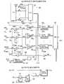
- FIG. 1is a configuration diagram of an A/D converter circuit showing a first embodiment of the present invention
- FIG. 2is a configuration diagram of a conventional A/D converter circuit
- FIG. 3is a signal waveform diagram showing operation of FIG. 1 ;
- FIG. 4is a configuration diagram illustrative of a comparator and a data holder showing a second embodiment of the present invention.
- FIG. 5is a configuration diagram of a timing controller showing a third embodiment of the present invention.
- FIGS. 1( a ) and 1 ( b )are configuration diagrams of an A/D converter circuit showing a first embodiment of the present invention.
- the present A/D converter circuitprocesses a multi-input (e.g., 256 inputs) and includes a sample and hold unit (S&H) 10 , a digital/analog converter (hereinafter called “DAC”) 20 and a binary counter 30 as shown in FIG. 1( a ).
- S&Hsample and hold unit
- DACdigital/analog converter
- Capacitors 13 i and buffers 14 iare respectively connected to the input terminals 11 i via switches 12 i .
- the capacitors 13 irespectively hold the input signals INi sampled by the switches 12 i and have other ends connected to a ground potential GND.
- the buffers 14 iare used to output analog voltages Ai at low impedance without changing the voltages (input signals INi) retained in the capacitors 13 i .
- the buffers 14 iare constituted of voltage-follower connected operational amplifiers or the like.
- the DAC 20outputs analog reference voltages REFs corresponding to a digital signal DIG.
- the DAC 20comprises a resistance voltage divider 21 which divides a voltage between a power supply potential VDD and the ground potential GND into voltages corresponding to 256 stages or levels, for example, switches 22 i for switching between the 256-level voltages divided by the resistance voltage divider 21 and outputting the switched voltages as the reference voltages REFs, respectively, and a decoder (DEC) 23 which decodes the digital value DIG and outputs signals for on/off-controlling the switches 22 i .
- DECdecoder
- the decoder 23is set in such a manner that its operation is controlled by a control signal DE and the switch 22 1 for outputting the ground potential GND is turned on when the operation thereof is prohibited.
- the DAC 20is configured such that when it is brought to an operating state by the control signal DE, the reference voltages REFs rise as the digital value DIG increases.
- the binary counter 30is of a 9-bit counter, for example. This counter counts a clock signal CLK and outputs its count value CNT therefrom. Lower 8 bits (bits b 0 through b 7 ) of the count value CNT are supplied to the decoder 23 as the digital value DIG.
- the A/D converter circuithas 256 comparators (CMPs) 40 i associated with the analog voltages Ai outputted from the sample and hold unit 10 , and 256 data holders 50 i corresponding thereto.
- the respective comparators 40 irespectively compare the analog voltages Ai and the reference voltages REFs.
- the comparators 40 ioutput decision signals Ri respectively brought to a level “L” when Ai ⁇ REFs and respectively brought to a level “H” when Ai ⁇ REFs.
- the respective data holders 50 iretain therein a digital value DIG when the decision signals Ri outputted from the comparators 40 i change from “L” to “H” and output the same as digital signals Di, respectively.
- the digital signals Di outputted from the respective data holders 50 iare supplied to a selector 60 .
- the selector 60selects the digital signals Di in accordance with the digital value DIG constituted of the lower 8 bits (bits b 0 through b 7 ) of the count value CNT when it is brought to an outputtable state by a control signal OE, and outputs the selected signal as an output signal OUT.
- the most significant bit b 8 of the binary counter 30is supplied to the DAC 20 as a control signal DE and inverted by inverters 31 and 32 , which inverted ones are then supplied as a control signal S/H for on/off-controlling the switches 12 1 through 12 256 of the sample and hold unit 10 and a control signal OE for controlling the selector 60 .
- the most significant bit b 8 and the clock signal CLKare supplied to an AND gate (hereinafter called “AND”) 33 .
- the clock signal CLK gate-controlled based on the most significant bit b 8is supplied to the respective data holders 50 i as a clock signal CK.
- each of the data holders 50 iare identical in configuration to one another.
- each of the data holderscomprises a change detection unit constituted of flip-flops (hereinafter called “FFs”) 51 and 52 and an AND 53 for detecting that the decision signal Ri has been changed from “L” to “H” and outputting a latch signal LAT, and a data latch 54 which latches a digital value DIG in response to the latch signal LAT and outputs the same as a digital signal Di.
- FFsflip-flops
- the data holderis configured in such a manner that the FFs 51 and 52 are connected in tandem and operated in sync with the common clock signal CK, an output terminal Q of the FF 51 and an inverse output terminal /Q of the FF 52 are connected to their corresponding input sides of the AND 53 , and the latch signal LAT is outputted from the output side of the AND 53 .
- FIG. 3is a signal waveform diagram showing the operation of FIG. 1 .
- the operation of the present A/D converter circuitis divided into a sampling/output period in which a count value CNT ranges from 0 to 255, and a conversion period in which the count value CNT ranges from 256 to 511.
- the operation of FIG. 1will be explained below with reference to FIG. 3 with being divided into a sampling/output operation (1) and a conversion operation (2).
- the control signal S/His brought to “H” and the switches 12 1 through 12 256 of the sample and hold unit 10 are all turned on.
- the input signals INi supplied to the respective input terminals 11 iare respectively applied to the capacitors 13 i via their corresponding switches 12 i .
- the capacitors 13 iare respectively charged to the same voltages as the input signals INi.
- the same voltages as the input signals INiare outputted from the buffers 14 i as their corresponding analog voltages Ai.
- the analog voltages Aialso change correspondingly.
- the operation of the selector 60is started. Since the digital value DIG is 0 at first, the digital signal D 1 of the data holder 50 1 is selected and outputted as an output OUT. When the digital value DIG is brought to 1 on the rising edge of the next clock signal CLK, the digital signal D 2 of the data holder 502 is selected and outputted as an output signal OUT. In like manner subsequently, the digital value DIG increases each time the clock signal CLK rises. The digital signals Di are sequentially outputted as output signals OUT according to the digital value DIG.
- a period during which the respective switches 12 i of the sample and hold unit 10 are onis 256 ⁇ s.
- the output of the clock signal CKis started from the AND 33 , and the operations of the change detection units of the respective data holders 50 i are started.
- the control signal DEis brought to “H”
- the operation of the decoder 23 in the DAC 20is started.
- the 256-level voltages divided by the resistance voltage divider 21are sequentially switched in accordance with the digital value DIG corresponding to the lower 8 bits of the count value CNT, after which they are outputted as their corresponding reference voltages REFs. That is, the reference voltages REFs rise stepwise from the ground potential GND to the power supply potential VDD in accordance with an increase in the digital value DIG.
- Each reference voltage REFis supplied to the respective comparators 40 i in common.
- the respective comparators 40 iare supplied with their corresponding analog voltages Ai associated with the input signals INi.
- the comparators 40 irespectively compare the analog signals Ai and the corresponding reference voltage REF and outputs decision signals Ri corresponding to the results of comparisons. Since the reference voltage REF rises stepwise from the ground potential GND to the power supply potential VDD, Ai ⁇ REF at first and the decision signals Ri are “L”.
- the decision signals Richange from “L” to “H”.
- latch signals LATsare outputted from the change detection units of the data holders 50 i , and a digital value DIG at that time is held in the data latches 54 as digital signals Di.
- the digital signal Di retained in each of the data latches 54indicates a digital value DIG at the moment that the reference voltage REF has exceeded the analog signals Ai, i.e., a value corresponding to the reference voltage REF nearly equal to the analog signals Ai.
- the digital signals Diare outputted as the output signals OUT when the count value CNT is returned to 0 after having been increased up to 511 and further the data holders 50 i are selected by the count value CNT.
- the A/D converter circuit according to the first embodimentis provided with the corresponding comparators 40 i every plural analog signals Ai, there is no need to provide selector switches on the output sides of the buffers 14 i of the sample and hold unit 10 . Further, the outputs signals (analog voltages Ai) of these buffers 14 i can always be supplied as the input signals of the comparators 40 i . Accordingly, the A/D converter circuit has advantages in that it is not necessary to prepare those large in drive capacity as the buffers 14 i and it is possible to shorten the conversion time without increasing its layout area and current consumption.
- the frequency of the clock signal CLKis set as 1 MHz in the first embodiment
- FIG. 4is a configuration diagram illustrative of one of comparators and one of data holders both showing a second embodiment of the present invention.
- the comparator 40 A and the data holder 50 Aare provided as an alternative to the comparators 40 i and the data holders 50 i shown in FIG. 1 .
- the comparator 40 Aproceeds to a low power consumption mode when a power control signal PD is given (when PD is brought to “H” in the present embodiment).
- the comparatorcan be configured by, for example, providing a switch in a power supply path of each comparator 40 shown in FIG. 1 and on/off-controlling the switch by the power control signal PD.
- the data holder 50 Aadditionally has the function of outputting a power control signal PD for the comparator 40 A in addition to the function of, when a decision signal Ri changes from “L” to “H”, latching a digital value DIG and outputting the same as a digital signal Di. That is, the data holder 50 A includes a set/reset type FF 55 in addition to a change detection unit or section comprising FFs 51 and 52 and an AND 53 , and a data latch 54 for latching a digital value DIG in response to a latch signal LAT outputted from the change detection unit, both of which are similar to those shown in FIG. 1( b ).
- the latch signal LATis applied to a set terminal S of the FF 55 , and a common reset signal RST is applied to its reset terminal R.
- a power control signal PDis outputted from an output terminal Q.
- the reset signal RSTis generated by a 9-bit AND 34 inputted with a control signal OE and an 8-bit digital value DIG in such a manner that it is supplied when the count value CNT is 255, for example.
- the data holder 50 A of the second embodimenthas the function of stopping the power control signal PD (bringing PD to “L”) only while it is detecting the change of the decision signal Ri from “L” to “H”.
- the comparator 40 Ais configured so as to operate only during a period in which the power control signal PD is being stopped.
- FIG. 5is a configuration diagram of a timing controller showing a third embodiment of the present invention.
- the timing controlleris provided as an alternative to the binary counter 30 and its peripheral inverters 31 and 32 and AND 33 shown in FIG. 1 in order to adapt to the arbitrary number m of input signals and the arbitrary number n of reference voltages.
- the timing controllerhas a selector 71 for selecting and outputting a clock signal CLK during a sampling period and a hold period.
- a counter 72 that counts from 0 to at least m-1 during the hold periodis connected to the first output side of the selector 71 .
- a counter 73 that counts from 0 to at least n-1 during the sampling periodis connected to the second output side of the selector 71 .
- Count values of the counters 72 and 73are applied to their corresponding first and second input sides of a selector 74 .
- the selector 74selects the count value of the counter 72 during the hold period, and selects the count value of the counter 73 during the sampling period and outputs it as a digital value DIG.
- the counters 72 and 73respectively have functions for outputting overflow signals OF 1 and OF 2 and reset functions for clearing them to 0 by their corresponding reset signals.
- the overflow signal OF 1 of the counter 72is applied to a reset terminal R of a set/reset type FF 75 and a reset terminal R of the counter 73 .
- the overflow signal OF 2 of the counter 73is applied to a set terminal S of the FF 75 and a reset terminal R of the counter 72 .
- An output signal S 75 of the FF 75is supplied to the selectors 71 and 74 as a selection signal and outputted as a control signal DE for a DAC 20 . Further, the output signal of the FF 75 is inverted by inverters 31 and 32 , from which the inverted signals are respectively applied to a sample and hold unit 10 and a selector 60 as control signals S/H and OE. A signal on the first output side of the selector 71 is supplied to respective data holders 50 i as a clock signal CK.
- the output signal S 75 of the FF 75is brought to, for example, “H” during the hold period, so that the first output side is selected at the selector 71 and the first input side is selected at the selector 74 .
- the counter 72is operated so that its count value is outputted from the selector 74 as a digital value DIG.
- the clock signal CK outputted from the first output side of the selector 71is supplied to the respective data holders 50 i .
- the overflow signal OF 1is outputted, so that the FF 75 and the counter 73 are reset.
- the output signal S 75 of the FF 75is brought to “L” and hence the sampling controller proceeds to the sampling period.
- the second output sideis selected at the selector 71 and the second input side is selected at the selector 74 .
- the counter 73is operated so that its count value is outputted from the selector 74 as a digital value DIG.
- the overflow signal OF 2is outputted so that the FF 75 is set and the counter 72 is reset.
- the output signal S 75 of the FF 75goes “H” and hence the timing controller proceeds to the hold period.
- the timing controller of the third embodimenthas the two counters 72 and 73 that respectively count the number m of input signals and the number n of reference voltages, and switches them depending on the hold period and the sampling period to output the digital value DIG.
- the timing controllerhas the advantage that the optimum timing control can be carried out corresponding to the arbitrary number m of input signals and the arbitrary number n of reference voltages.
- the present inventionis, not limited to the above embodiments.
- Various modificationscan be made thereto.
- the modificationsthe following are cited for instance.
- the binary counter 30may be configured so as to be able to count its maximum count value up to twice the large one of m and n.
- the binary counter 30is set to 9 bits. Since, in this case, the corresponding data holder 50 does not exist during the period from 128 to 255 of the digital value DIG at the sampling and output operating periods, no effective output OUT is outputted.
- the binary counter 30is set to 9 bits.
- the DAC 20is configured so as to always output the power supply potential VDD as the reference voltage REF when the digital value DIG ranges from 128 to 255.
- the DAC 20is not limited to the configurations illustrated in the figures. If, for example, a weighting resistance type, a ladder resistance type or the like is used, then the circuit can be simplified because each switch is directly controlled by a binary digital value DIG without using the decoder 23 .
- the DAC 20may be configured in such a manner that each of the reference voltages REFs rises stepwise as the digital value DIG increases.
- the DAC 20may be configured in such a manner that the reference voltage REF is lowered stepwise contrary to this.
- the levels of the decision signals Ri outputted from the respective comparators 40 imay be inverted.
- the configurations of the respective data holders 50 imay be changed in such a manner that the digital value DIG is held when the decision signals Ri have changed from “H” to “L”.
- each of the comparators 40 i shown in FIG. 1may be changed to the power controllable comparator 40 A shown in FIG. 4 to supply the control signal OE as a power control signal.
- each of the comparators 40 Ais brought into an operating state during a conversion operating period in which the count value CNT ranges from 256 to 511.
- sampling and output operationsare carried out at the first half of the count value CNT and the conversion operation is carried out at its latter half, they may be set in reverse.
Landscapes
- Engineering & Computer Science (AREA)
- Theoretical Computer Science (AREA)
- Analogue/Digital Conversion (AREA)
Abstract
Description
Claims (3)
Applications Claiming Priority (2)
| Application Number | Priority Date | Filing Date | Title |
|---|---|---|---|
| JP2006-033594 | 2006-02-10 | ||
| JP2006033594AJP4705858B2 (en) | 2006-02-10 | 2006-02-10 | Analog / digital conversion circuit |
Publications (2)
| Publication Number | Publication Date |
|---|---|
| US20070188367A1 US20070188367A1 (en) | 2007-08-16 |
| US7372390B2true US7372390B2 (en) | 2008-05-13 |
Family
ID=38367808
Family Applications (1)
| Application Number | Title | Priority Date | Filing Date |
|---|---|---|---|
| US11/655,172ActiveUS7372390B2 (en) | 2006-02-10 | 2007-01-19 | Analog-digital converter circuit |
Country Status (4)
| Country | Link |
|---|---|
| US (1) | US7372390B2 (en) |
| JP (1) | JP4705858B2 (en) |
| KR (1) | KR101312813B1 (en) |
| CN (1) | CN101018058B (en) |
Cited By (57)
| Publication number | Priority date | Publication date | Assignee | Title |
|---|---|---|---|---|
| US20090244044A1 (en)* | 2008-03-27 | 2009-10-01 | Oki Semiconductor Co., Ltd. | Display driver circuit for driving a light-emitting device with the threshold offset of a drive transistor compensated for |
| US20100195776A1 (en)* | 2008-06-06 | 2010-08-05 | Erik Chmelar | Systems and Methods for Synchronous, Retimed Analog to Digital Conversion |
| US20130169461A1 (en)* | 2011-07-06 | 2013-07-04 | Qualcomm Incorporated | Digital-to-analog converter circuitry with weighted resistance elements |
| US9485057B2 (en) | 2010-05-20 | 2016-11-01 | Kandou Labs, S.A. | Vector signaling with reduced receiver complexity |
| US9524106B1 (en) | 2012-05-14 | 2016-12-20 | Kandou Labs, S.A. | Storage method and apparatus for random access memory using codeword storage |
| US9544015B2 (en) | 2014-06-25 | 2017-01-10 | Kandou Labs, S.A. | Multilevel driver for high speed chip-to-chip communications |
| US9577664B2 (en) | 2010-05-20 | 2017-02-21 | Kandou Labs, S.A. | Efficient processing and detection of balanced codes |
| US9674014B2 (en) | 2014-10-22 | 2017-06-06 | Kandou Labs, S.A. | Method and apparatus for high speed chip-to-chip communications |
| US9686107B2 (en) | 2010-05-20 | 2017-06-20 | Kandou Labs, S.A. | Methods and systems for chip-to-chip communication with reduced simultaneous switching noise |
| US9686106B2 (en) | 2014-02-28 | 2017-06-20 | Kandou Labs, S.A. | Clock-embedded vector signaling codes |
| US9692381B2 (en) | 2014-05-16 | 2017-06-27 | Kandou Labs, S.A. | Symmetric linear equalization circuit with increased gain |
| US9806761B1 (en) | 2014-01-31 | 2017-10-31 | Kandou Labs, S.A. | Methods and systems for reduction of nearest-neighbor crosstalk |
| US9819522B2 (en) | 2010-05-20 | 2017-11-14 | Kandou Labs, S.A. | Circuits for efficient detection of vector signaling codes for chip-to-chip communication |
| US9825723B2 (en) | 2010-05-20 | 2017-11-21 | Kandou Labs, S.A. | Methods and systems for skew tolerance in and advanced detectors for vector signaling codes for chip-to-chip communication |
| US9825677B2 (en) | 2010-04-30 | 2017-11-21 | ECOLE POLYTECHNIQUE FéDéRALE DE LAUSANNE | Orthogonal differential vector signaling |
| US9832046B2 (en) | 2015-06-26 | 2017-11-28 | Kandou Labs, S.A. | High speed communications system |
| US9838017B2 (en) | 2010-05-20 | 2017-12-05 | Kandou Labs, S.A. | Methods and systems for high bandwidth chip-to-chip communcations interface |
| US9838234B2 (en) | 2014-08-01 | 2017-12-05 | Kandou Labs, S.A. | Orthogonal differential vector signaling codes with embedded clock |
| US9852806B2 (en) | 2014-06-20 | 2017-12-26 | Kandou Labs, S.A. | System for generating a test pattern to detect and isolate stuck faults for an interface using transition coding |
| US9893911B2 (en) | 2014-07-21 | 2018-02-13 | Kandou Labs, S.A. | Multidrop data transfer |
| US9900186B2 (en) | 2014-07-10 | 2018-02-20 | Kandou Labs, S.A. | Vector signaling codes with increased signal to noise characteristics |
| US9906358B1 (en) | 2016-08-31 | 2018-02-27 | Kandou Labs, S.A. | Lock detector for phase lock loop |
| US9985634B2 (en) | 2010-05-20 | 2018-05-29 | Kandou Labs, S.A. | Data-driven voltage regulator |
| US9985745B2 (en) | 2013-06-25 | 2018-05-29 | Kandou Labs, S.A. | Vector signaling with reduced receiver complexity |
| US10003424B2 (en) | 2014-07-17 | 2018-06-19 | Kandou Labs, S.A. | Bus reversible orthogonal differential vector signaling codes |
| US10003454B2 (en) | 2016-04-22 | 2018-06-19 | Kandou Labs, S.A. | Sampler with low input kickback |
| US10003315B2 (en) | 2016-01-25 | 2018-06-19 | Kandou Labs S.A. | Voltage sampler driver with enhanced high-frequency gain |
| US10056903B2 (en) | 2016-04-28 | 2018-08-21 | Kandou Labs, S.A. | Low power multilevel driver |
| US10055372B2 (en) | 2015-11-25 | 2018-08-21 | Kandou Labs, S.A. | Orthogonal differential vector signaling codes with embedded clock |
| US10057049B2 (en) | 2016-04-22 | 2018-08-21 | Kandou Labs, S.A. | High performance phase locked loop |
| US10091035B2 (en) | 2013-04-16 | 2018-10-02 | Kandou Labs, S.A. | Methods and systems for high bandwidth communications interface |
| US10116468B1 (en) | 2017-06-28 | 2018-10-30 | Kandou Labs, S.A. | Low power chip-to-chip bidirectional communications |
| US10153591B2 (en) | 2016-04-28 | 2018-12-11 | Kandou Labs, S.A. | Skew-resistant multi-wire channel |
| US10200218B2 (en) | 2016-10-24 | 2019-02-05 | Kandou Labs, S.A. | Multi-stage sampler with increased gain |
| US10200188B2 (en) | 2016-10-21 | 2019-02-05 | Kandou Labs, S.A. | Quadrature and duty cycle error correction in matrix phase lock loop |
| US10203226B1 (en) | 2017-08-11 | 2019-02-12 | Kandou Labs, S.A. | Phase interpolation circuit |
| US10277431B2 (en) | 2016-09-16 | 2019-04-30 | Kandou Labs, S.A. | Phase rotation circuit for eye scope measurements |
| US10326623B1 (en) | 2017-12-08 | 2019-06-18 | Kandou Labs, S.A. | Methods and systems for providing multi-stage distributed decision feedback equalization |
| US10333741B2 (en) | 2016-04-28 | 2019-06-25 | Kandou Labs, S.A. | Vector signaling codes for densely-routed wire groups |
| US10333749B2 (en) | 2014-05-13 | 2019-06-25 | Kandou Labs, S.A. | Vector signaling code with improved noise margin |
| US10348436B2 (en) | 2014-02-02 | 2019-07-09 | Kandou Labs, S.A. | Method and apparatus for low power chip-to-chip communications with constrained ISI ratio |
| US10372665B2 (en) | 2016-10-24 | 2019-08-06 | Kandou Labs, S.A. | Multiphase data receiver with distributed DFE |
| US10468078B2 (en) | 2010-05-20 | 2019-11-05 | Kandou Labs, S.A. | Methods and systems for pin-efficient memory controller interface using vector signaling codes for chip-to-chip communication |
| US10554380B2 (en) | 2018-01-26 | 2020-02-04 | Kandou Labs, S.A. | Dynamically weighted exclusive or gate having weighted output segments for phase detection and phase interpolation |
| US10574487B1 (en) | 2019-04-08 | 2020-02-25 | Kandou Labs, S.A. | Sampler offset calibration during operation |
| US10608849B1 (en) | 2019-04-08 | 2020-03-31 | Kandou Labs, S.A. | Variable gain amplifier and sampler offset calibration without clock recovery |
| US10680634B1 (en) | 2019-04-08 | 2020-06-09 | Kandou Labs, S.A. | Dynamic integration time adjustment of a clocked data sampler using a static analog calibration circuit |
| US10679716B2 (en) | 2016-04-22 | 2020-06-09 | Kandou Labs, S.A. | Calibration apparatus and method for sampler with adjustable high frequency gain |
| US10686583B2 (en) | 2017-07-04 | 2020-06-16 | Kandou Labs, S.A. | Method for measuring and correcting multi-wire skew |
| US10721106B1 (en) | 2019-04-08 | 2020-07-21 | Kandou Labs, S.A. | Adaptive continuous time linear equalization and channel bandwidth control |
| US10742451B2 (en) | 2018-06-12 | 2020-08-11 | Kandou Labs, S.A. | Passive multi-input comparator for orthogonal codes on a multi-wire bus |
| US10931249B2 (en) | 2018-06-12 | 2021-02-23 | Kandou Labs, S.A. | Amplifier with adjustable high-frequency gain using varactor diodes |
| US11183983B2 (en) | 2018-09-10 | 2021-11-23 | Kandou Labs, S.A. | Programmable continuous time linear equalizer having stabilized high-frequency peaking for controlling operating current of a slicer |
| US11303484B1 (en) | 2021-04-02 | 2022-04-12 | Kandou Labs SA | Continuous time linear equalization and bandwidth adaptation using asynchronous sampling |
| US11374800B1 (en) | 2021-04-14 | 2022-06-28 | Kandou Labs SA | Continuous time linear equalization and bandwidth adaptation using peak detector |
| US11456708B1 (en) | 2021-04-30 | 2022-09-27 | Kandou Labs SA | Reference generation circuit for maintaining temperature-tracked linearity in amplifier with adjustable high-frequency gain |
| US12355409B2 (en) | 2022-03-24 | 2025-07-08 | Kandou Labs SA | Variable gain amplifier with cross-coupled common mode reduction |
Families Citing this family (35)
| Publication number | Priority date | Publication date | Assignee | Title |
|---|---|---|---|---|
| JP4970224B2 (en)* | 2007-11-30 | 2012-07-04 | ルネサスエレクトロニクス株式会社 | Semiconductor integrated circuit |
| JP2009159069A (en) | 2007-12-25 | 2009-07-16 | Panasonic Corp | Solid-state imaging device and camera |
| JP5123655B2 (en)* | 2007-12-26 | 2013-01-23 | パナソニック株式会社 | Solid-state imaging device |
| US7746260B1 (en)* | 2008-12-19 | 2010-06-29 | Mediatek Inc. | Multiplying digital-to-analog converter for high speed and low supply voltage |
| JP5313008B2 (en)* | 2009-03-30 | 2013-10-09 | オリンパス株式会社 | Correction signal generator and A / D converter |
| JP2010268349A (en)* | 2009-05-18 | 2010-11-25 | Renesas Electronics Corp | Analog / digital conversion circuit and analog / digital conversion method |
| US8390497B2 (en)* | 2010-05-18 | 2013-03-05 | Linear Technology Corporation | Method and circuit for encoding and transmitting numerical values from an analog-to-digital conversion process |
| US9596109B2 (en) | 2010-05-20 | 2017-03-14 | Kandou Labs, S.A. | Methods and systems for high bandwidth communications interface |
| US9450744B2 (en) | 2010-05-20 | 2016-09-20 | Kandou Lab, S.A. | Control loop management and vector signaling code communications links |
| US9401828B2 (en) | 2010-05-20 | 2016-07-26 | Kandou Labs, S.A. | Methods and systems for low-power and pin-efficient communications with superposition signaling codes |
| US9564994B2 (en) | 2010-05-20 | 2017-02-07 | Kandou Labs, S.A. | Fault tolerant chip-to-chip communication with advanced voltage |
| US9362962B2 (en) | 2010-05-20 | 2016-06-07 | Kandou Labs, S.A. | Methods and systems for energy-efficient communications interface |
| US9106238B1 (en)* | 2010-12-30 | 2015-08-11 | Kandou Labs, S.A. | Sorting decoder |
| CN102055477B (en)* | 2010-11-29 | 2012-03-21 | 复旦大学 | Amplitude-interleaving analog digital composite signal processing circuit |
| US9275720B2 (en) | 2010-12-30 | 2016-03-01 | Kandou Labs, S.A. | Differential vector storage for dynamic random access memory |
| US8633753B2 (en)* | 2012-02-09 | 2014-01-21 | Analog Devices, Inc. | Clock distribution system and method for a multi-bit latch |
| KR101446289B1 (en)* | 2012-10-11 | 2014-10-06 | 연세대학교 산학협력단 | Time to digital converter and method for converting time to digital |
| US8902093B1 (en)* | 2012-12-05 | 2014-12-02 | Cadence Design Systems, Inc. | Parallel analog to digital converter architecture with charge redistribution and method thereof |
| JP6111662B2 (en)* | 2012-12-28 | 2017-04-12 | 富士通株式会社 | Analog / digital converter |
| CN103281051A (en)* | 2013-05-22 | 2013-09-04 | 山东大学 | Quick-response low-drift active low-pass filter circuit |
| CN103312331B (en)* | 2013-05-30 | 2016-04-13 | 电子科技大学 | A kind of analog to digital converter based on memristor |
| US9106465B2 (en) | 2013-11-22 | 2015-08-11 | Kandou Labs, S.A. | Multiwire linear equalizer for vector signaling code receiver |
| US9369312B1 (en) | 2014-02-02 | 2016-06-14 | Kandou Labs, S.A. | Low EMI signaling for parallel conductor interfaces |
| US9397676B1 (en)* | 2015-09-29 | 2016-07-19 | Analog Devices, Inc. | Low power switching techniques for digital-to-analog converters |
| US9876421B2 (en)* | 2015-10-09 | 2018-01-23 | Semiconductor Components Industries, Llc | Power supply controller and related methods |
| US9557760B1 (en) | 2015-10-28 | 2017-01-31 | Kandou Labs, S.A. | Enhanced phase interpolation circuit |
| US9577815B1 (en) | 2015-10-29 | 2017-02-21 | Kandou Labs, S.A. | Clock data alignment system for vector signaling code communications link |
| US9847839B2 (en)* | 2016-03-04 | 2017-12-19 | Inphi Corporation | PAM4 transceivers for high-speed communication |
| US11265006B2 (en)* | 2018-08-08 | 2022-03-01 | Infineon Technologies Ag | Using a sampling switch for multiple evaluation units |
| CN113556127B (en)* | 2020-04-23 | 2024-03-12 | 瑞昱半导体股份有限公司 | Digital slope type analog-digital converter device and signal conversion method |
| CN112152626B (en)* | 2020-09-29 | 2024-06-14 | 珠海格力电器股份有限公司 | Analog-to-digital conversion acquisition circuit and chip |
| JPWO2022102002A1 (en)* | 2020-11-11 | 2022-05-19 | ||
| CN114665878A (en)* | 2022-04-06 | 2022-06-24 | 上海联影微电子科技有限公司 | Analog-digital conversion circuit |
| JP2024040917A (en)* | 2022-09-13 | 2024-03-26 | キオクシア株式会社 | Semiconductor integrated circuit and receiver |
| CN119420360A (en)* | 2025-01-06 | 2025-02-11 | 安徽大学 | Successive approximation analog-to-digital converter circuit and its reference voltage circuit |
Citations (6)
| Publication number | Priority date | Publication date | Assignee | Title |
|---|---|---|---|---|
| US5061926A (en)* | 1988-11-07 | 1991-10-29 | Kawai Musical Instruments Mfg. Co., Ltd. | AD converter using successive comparison |
| JPH0738439A (en) | 1993-07-26 | 1995-02-07 | Mitsubishi Electric Corp | A / D converter |
| US5861829A (en)* | 1997-04-28 | 1999-01-19 | Marvell Technology Group, Ltd. | High-speed, low power, medium resolution analog-to-digital converter and method of stabilization |
| US5936566A (en)* | 1997-09-12 | 1999-08-10 | Conexant Systems, Inc. | Auto-reference pseudo-flash analog to digital converter |
| US6107949A (en)* | 1997-02-24 | 2000-08-22 | Lucent Technologies Inc. | Flash analog-to-digital converter with matrix-switched comparators |
| US7102559B2 (en)* | 2003-01-17 | 2006-09-05 | Koninklijke Philips Electronics, N.V. | Analog-to-digital converter having interleaved coarse sections coupled to a single fine section |
Family Cites Families (7)
| Publication number | Priority date | Publication date | Assignee | Title |
|---|---|---|---|---|
| JPS58164317A (en)* | 1982-03-24 | 1983-09-29 | Casio Comput Co Ltd | Current reduction method of A-D converter |
| JPS6288430A (en)* | 1985-10-14 | 1987-04-22 | Nippon Denso Co Ltd | Analog-digital converter |
| JP2636861B2 (en)* | 1987-12-01 | 1997-07-30 | 株式会社リコー | Analog / digital converter |
| JP2952786B2 (en)* | 1990-09-20 | 1999-09-27 | 株式会社日立製作所 | AD converter |
| IL118403A (en)* | 1995-05-25 | 2001-09-13 | Lockheed Martin Ir Imaging Sys | Monolithic analog-digital converter and method for the same |
| JP3507800B2 (en)* | 2001-02-02 | 2004-03-15 | 有限会社リニアセル・デザイン | Analog-digital converter and image sensor using the same |
| JP2003060507A (en)* | 2001-08-17 | 2003-02-28 | Innotech Corp | Lamp voltage generation circuit and analog-to-digital converter using the same |
- 2006
- 2006-02-10JPJP2006033594Apatent/JP4705858B2/ennot_activeExpired - Fee Related
- 2007
- 2007-01-19USUS11/655,172patent/US7372390B2/enactiveActive
- 2007-01-25KRKR1020070007995Apatent/KR101312813B1/ennot_activeExpired - Fee Related
- 2007-01-31CNCN2007100069717Apatent/CN101018058B/ennot_activeExpired - Fee Related
Patent Citations (6)
| Publication number | Priority date | Publication date | Assignee | Title |
|---|---|---|---|---|
| US5061926A (en)* | 1988-11-07 | 1991-10-29 | Kawai Musical Instruments Mfg. Co., Ltd. | AD converter using successive comparison |
| JPH0738439A (en) | 1993-07-26 | 1995-02-07 | Mitsubishi Electric Corp | A / D converter |
| US6107949A (en)* | 1997-02-24 | 2000-08-22 | Lucent Technologies Inc. | Flash analog-to-digital converter with matrix-switched comparators |
| US5861829A (en)* | 1997-04-28 | 1999-01-19 | Marvell Technology Group, Ltd. | High-speed, low power, medium resolution analog-to-digital converter and method of stabilization |
| US5936566A (en)* | 1997-09-12 | 1999-08-10 | Conexant Systems, Inc. | Auto-reference pseudo-flash analog to digital converter |
| US7102559B2 (en)* | 2003-01-17 | 2006-09-05 | Koninklijke Philips Electronics, N.V. | Analog-to-digital converter having interleaved coarse sections coupled to a single fine section |
Cited By (94)
| Publication number | Priority date | Publication date | Assignee | Title |
|---|---|---|---|---|
| US20090244044A1 (en)* | 2008-03-27 | 2009-10-01 | Oki Semiconductor Co., Ltd. | Display driver circuit for driving a light-emitting device with the threshold offset of a drive transistor compensated for |
| US8125417B2 (en) | 2008-03-27 | 2012-02-28 | Oki Semiconductor Co., Ltd. | Display driver circuit for driving a light-emitting device with the threshold offset of a drive transistor compensated for |
| US20100195776A1 (en)* | 2008-06-06 | 2010-08-05 | Erik Chmelar | Systems and Methods for Synchronous, Retimed Analog to Digital Conversion |
| US7973692B2 (en)* | 2008-06-06 | 2011-07-05 | Lsi Corporation | Systems and methods for synchronous, retimed analog to digital conversion |
| JP2011523294A (en)* | 2008-06-06 | 2011-08-04 | エルエスアイ コーポレーション | System and method for latch-based analog-to-digital conversion |
| US9825677B2 (en) | 2010-04-30 | 2017-11-21 | ECOLE POLYTECHNIQUE FéDéRALE DE LAUSANNE | Orthogonal differential vector signaling |
| US9692555B2 (en) | 2010-05-20 | 2017-06-27 | Kandou Labs, S.A. | Vector signaling with reduced receiver complexity |
| US9929818B2 (en) | 2010-05-20 | 2018-03-27 | Kandou Bus, S.A. | Methods and systems for selection of unions of vector signaling codes for power and pin efficient chip-to-chip communication |
| US10044452B2 (en) | 2010-05-20 | 2018-08-07 | Kandou Labs, S.A. | Methods and systems for skew tolerance in and advanced detectors for vector signaling codes for chip-to-chip communication |
| US9985634B2 (en) | 2010-05-20 | 2018-05-29 | Kandou Labs, S.A. | Data-driven voltage regulator |
| US9577664B2 (en) | 2010-05-20 | 2017-02-21 | Kandou Labs, S.A. | Efficient processing and detection of balanced codes |
| US9838017B2 (en) | 2010-05-20 | 2017-12-05 | Kandou Labs, S.A. | Methods and systems for high bandwidth chip-to-chip communcations interface |
| US9686107B2 (en) | 2010-05-20 | 2017-06-20 | Kandou Labs, S.A. | Methods and systems for chip-to-chip communication with reduced simultaneous switching noise |
| US9485057B2 (en) | 2010-05-20 | 2016-11-01 | Kandou Labs, S.A. | Vector signaling with reduced receiver complexity |
| US9825723B2 (en) | 2010-05-20 | 2017-11-21 | Kandou Labs, S.A. | Methods and systems for skew tolerance in and advanced detectors for vector signaling codes for chip-to-chip communication |
| US10468078B2 (en) | 2010-05-20 | 2019-11-05 | Kandou Labs, S.A. | Methods and systems for pin-efficient memory controller interface using vector signaling codes for chip-to-chip communication |
| US9819522B2 (en) | 2010-05-20 | 2017-11-14 | Kandou Labs, S.A. | Circuits for efficient detection of vector signaling codes for chip-to-chip communication |
| US10164809B2 (en) | 2010-12-30 | 2018-12-25 | Kandou Labs, S.A. | Circuits for efficient detection of vector signaling codes for chip-to-chip communication |
| US10560293B2 (en) | 2010-12-30 | 2020-02-11 | Kandou Labs, S.A. | Circuits for efficient detection of vector signaling codes for chip-to-chip communication |
| US10574370B2 (en) | 2010-12-30 | 2020-02-25 | Kandou Labs, S.A. | Methods and systems for skew tolerance in and advanced detectors for vector signaling codes for chip-to-chip communication |
| US8860597B2 (en)* | 2011-07-06 | 2014-10-14 | Qualcomm Incorporated | Digital to-analog converter circuitry with weighted resistance elements |
| US20130169461A1 (en)* | 2011-07-06 | 2013-07-04 | Qualcomm Incorporated | Digital-to-analog converter circuitry with weighted resistance elements |
| US9524106B1 (en) | 2012-05-14 | 2016-12-20 | Kandou Labs, S.A. | Storage method and apparatus for random access memory using codeword storage |
| US10091035B2 (en) | 2013-04-16 | 2018-10-02 | Kandou Labs, S.A. | Methods and systems for high bandwidth communications interface |
| US9985745B2 (en) | 2013-06-25 | 2018-05-29 | Kandou Labs, S.A. | Vector signaling with reduced receiver complexity |
| US9806761B1 (en) | 2014-01-31 | 2017-10-31 | Kandou Labs, S.A. | Methods and systems for reduction of nearest-neighbor crosstalk |
| US10177812B2 (en) | 2014-01-31 | 2019-01-08 | Kandou Labs, S.A. | Methods and systems for reduction of nearest-neighbor crosstalk |
| US10348436B2 (en) | 2014-02-02 | 2019-07-09 | Kandou Labs, S.A. | Method and apparatus for low power chip-to-chip communications with constrained ISI ratio |
| US9686106B2 (en) | 2014-02-28 | 2017-06-20 | Kandou Labs, S.A. | Clock-embedded vector signaling codes |
| US10020966B2 (en) | 2014-02-28 | 2018-07-10 | Kandou Labs, S.A. | Vector signaling codes with high pin-efficiency for chip-to-chip communication and storage |
| US10333749B2 (en) | 2014-05-13 | 2019-06-25 | Kandou Labs, S.A. | Vector signaling code with improved noise margin |
| US9692381B2 (en) | 2014-05-16 | 2017-06-27 | Kandou Labs, S.A. | Symmetric linear equalization circuit with increased gain |
| US9852806B2 (en) | 2014-06-20 | 2017-12-26 | Kandou Labs, S.A. | System for generating a test pattern to detect and isolate stuck faults for an interface using transition coding |
| US9544015B2 (en) | 2014-06-25 | 2017-01-10 | Kandou Labs, S.A. | Multilevel driver for high speed chip-to-chip communications |
| US9917711B2 (en) | 2014-06-25 | 2018-03-13 | Kandou Labs, S.A. | Multilevel driver for high speed chip-to-chip communications |
| US10091033B2 (en) | 2014-06-25 | 2018-10-02 | Kandou Labs, S.A. | Multilevel driver for high speed chip-to-chip communications |
| US10320588B2 (en) | 2014-07-10 | 2019-06-11 | Kandou Labs, S.A. | Vector signaling codes with increased signal to noise characteristics |
| US9900186B2 (en) | 2014-07-10 | 2018-02-20 | Kandou Labs, S.A. | Vector signaling codes with increased signal to noise characteristics |
| US10003424B2 (en) | 2014-07-17 | 2018-06-19 | Kandou Labs, S.A. | Bus reversible orthogonal differential vector signaling codes |
| US9893911B2 (en) | 2014-07-21 | 2018-02-13 | Kandou Labs, S.A. | Multidrop data transfer |
| US10230549B2 (en) | 2014-07-21 | 2019-03-12 | Kandou Labs, S.A. | Multidrop data transfer |
| US9838234B2 (en) | 2014-08-01 | 2017-12-05 | Kandou Labs, S.A. | Orthogonal differential vector signaling codes with embedded clock |
| US10122561B2 (en) | 2014-08-01 | 2018-11-06 | Kandou Labs, S.A. | Orthogonal differential vector signaling codes with embedded clock |
| US9674014B2 (en) | 2014-10-22 | 2017-06-06 | Kandou Labs, S.A. | Method and apparatus for high speed chip-to-chip communications |
| US10243765B2 (en) | 2014-10-22 | 2019-03-26 | Kandou Labs, S.A. | Method and apparatus for high speed chip-to-chip communications |
| US10116472B2 (en) | 2015-06-26 | 2018-10-30 | Kandou Labs, S.A. | High speed communications system |
| US9832046B2 (en) | 2015-06-26 | 2017-11-28 | Kandou Labs, S.A. | High speed communications system |
| US10055372B2 (en) | 2015-11-25 | 2018-08-21 | Kandou Labs, S.A. | Orthogonal differential vector signaling codes with embedded clock |
| US10498305B2 (en) | 2016-01-25 | 2019-12-03 | Kandou Labs, S.A. | Voltage sampler driver with enhanced high-frequency gain |
| US10003315B2 (en) | 2016-01-25 | 2018-06-19 | Kandou Labs S.A. | Voltage sampler driver with enhanced high-frequency gain |
| US11183982B2 (en) | 2016-01-25 | 2021-11-23 | Kandou Labs, S.A. | Voltage sampler driver with enhanced high-frequency gain |
| US10003454B2 (en) | 2016-04-22 | 2018-06-19 | Kandou Labs, S.A. | Sampler with low input kickback |
| US10057049B2 (en) | 2016-04-22 | 2018-08-21 | Kandou Labs, S.A. | High performance phase locked loop |
| US10679716B2 (en) | 2016-04-22 | 2020-06-09 | Kandou Labs, S.A. | Calibration apparatus and method for sampler with adjustable high frequency gain |
| US10673608B2 (en) | 2016-04-22 | 2020-06-02 | Kandou Labs, S.A. | Sampler with low input kickback |
| US10056903B2 (en) | 2016-04-28 | 2018-08-21 | Kandou Labs, S.A. | Low power multilevel driver |
| US10333741B2 (en) | 2016-04-28 | 2019-06-25 | Kandou Labs, S.A. | Vector signaling codes for densely-routed wire groups |
| US10153591B2 (en) | 2016-04-28 | 2018-12-11 | Kandou Labs, S.A. | Skew-resistant multi-wire channel |
| US9906358B1 (en) | 2016-08-31 | 2018-02-27 | Kandou Labs, S.A. | Lock detector for phase lock loop |
| US10355852B2 (en) | 2016-08-31 | 2019-07-16 | Kandou Labs, S.A. | Lock detector for phase lock loop |
| US10277431B2 (en) | 2016-09-16 | 2019-04-30 | Kandou Labs, S.A. | Phase rotation circuit for eye scope measurements |
| US10200188B2 (en) | 2016-10-21 | 2019-02-05 | Kandou Labs, S.A. | Quadrature and duty cycle error correction in matrix phase lock loop |
| US10200218B2 (en) | 2016-10-24 | 2019-02-05 | Kandou Labs, S.A. | Multi-stage sampler with increased gain |
| US10372665B2 (en) | 2016-10-24 | 2019-08-06 | Kandou Labs, S.A. | Multiphase data receiver with distributed DFE |
| US10608847B2 (en) | 2016-10-24 | 2020-03-31 | Kandou Labs, S.A. | Multi-stage sampler with increased gain |
| US10116468B1 (en) | 2017-06-28 | 2018-10-30 | Kandou Labs, S.A. | Low power chip-to-chip bidirectional communications |
| US10686583B2 (en) | 2017-07-04 | 2020-06-16 | Kandou Labs, S.A. | Method for measuring and correcting multi-wire skew |
| US10203226B1 (en) | 2017-08-11 | 2019-02-12 | Kandou Labs, S.A. | Phase interpolation circuit |
| US10326623B1 (en) | 2017-12-08 | 2019-06-18 | Kandou Labs, S.A. | Methods and systems for providing multi-stage distributed decision feedback equalization |
| US10554380B2 (en) | 2018-01-26 | 2020-02-04 | Kandou Labs, S.A. | Dynamically weighted exclusive or gate having weighted output segments for phase detection and phase interpolation |
| US11159350B2 (en) | 2018-06-12 | 2021-10-26 | Kandou Labs, S.A. | Passive multi-input comparator for orthogonal codes on a multi-wire bus |
| US11502658B2 (en) | 2018-06-12 | 2022-11-15 | Kandou Labs, S.A. | Amplifier with adjustable high-frequency gain using varactor diodes |
| US10931249B2 (en) | 2018-06-12 | 2021-02-23 | Kandou Labs, S.A. | Amplifier with adjustable high-frequency gain using varactor diodes |
| US10742451B2 (en) | 2018-06-12 | 2020-08-11 | Kandou Labs, S.A. | Passive multi-input comparator for orthogonal codes on a multi-wire bus |
| US11183983B2 (en) | 2018-09-10 | 2021-11-23 | Kandou Labs, S.A. | Programmable continuous time linear equalizer having stabilized high-frequency peaking for controlling operating current of a slicer |
| US11627022B2 (en) | 2019-04-08 | 2023-04-11 | Kandou Labs, S.A. | Variable gain amplifier and sampler offset calibration without clock recovery |
| US10680634B1 (en) | 2019-04-08 | 2020-06-09 | Kandou Labs, S.A. | Dynamic integration time adjustment of a clocked data sampler using a static analog calibration circuit |
| US11038518B2 (en) | 2019-04-08 | 2021-06-15 | Kandou Labs, S.A. | Dynamic integration time adjustment of a clocked data sampler using a static analog calibration circuit |
| US10848351B2 (en) | 2019-04-08 | 2020-11-24 | Kandou Labs, S.A. | Sampler offset calibration during operation |
| US10608849B1 (en) | 2019-04-08 | 2020-03-31 | Kandou Labs, S.A. | Variable gain amplifier and sampler offset calibration without clock recovery |
| US10574487B1 (en) | 2019-04-08 | 2020-02-25 | Kandou Labs, S.A. | Sampler offset calibration during operation |
| US10904046B2 (en) | 2019-04-08 | 2021-01-26 | Kandou Labs, S.A. | Variable gain amplifier and sampler offset calibration without clock recovery |
| US11265190B2 (en) | 2019-04-08 | 2022-03-01 | Kandou Labs, S.A. | Variable gain amplifier and sampler offset calibration without clock recovery |
| US10721106B1 (en) | 2019-04-08 | 2020-07-21 | Kandou Labs, S.A. | Adaptive continuous time linear equalization and channel bandwidth control |
| US11515885B2 (en) | 2019-04-08 | 2022-11-29 | Kandou Labs, S.A. | Dynamic integration time adjustment of a clocked data sampler using a static analog calibration circuit |
| US11115246B2 (en) | 2019-04-08 | 2021-09-07 | Kandou Labs, S.A. | Sampler offset calibration during operation |
| US11575549B2 (en) | 2021-04-02 | 2023-02-07 | Kandou Labs SA | Continuous time linear equalization and bandwidth adaptation using asynchronous sampling |
| US11303484B1 (en) | 2021-04-02 | 2022-04-12 | Kandou Labs SA | Continuous time linear equalization and bandwidth adaptation using asynchronous sampling |
| US11838156B2 (en) | 2021-04-02 | 2023-12-05 | Kandou Labs SA | Continuous time linear equalization and bandwidth adaptation using asynchronous sampling |
| US11374800B1 (en) | 2021-04-14 | 2022-06-28 | Kandou Labs SA | Continuous time linear equalization and bandwidth adaptation using peak detector |
| US11722341B2 (en) | 2021-04-14 | 2023-08-08 | Kandou Labs SA | Continuous time linear equalization and bandwidth adaptation using peak detector |
| US11456708B1 (en) | 2021-04-30 | 2022-09-27 | Kandou Labs SA | Reference generation circuit for maintaining temperature-tracked linearity in amplifier with adjustable high-frequency gain |
| US12224715B2 (en) | 2021-04-30 | 2025-02-11 | Kandou Labs SA | Reference generation circuit for maintaining temperature-tracked linearity in amplifier with adjustable high-frequency gain |
| US12355409B2 (en) | 2022-03-24 | 2025-07-08 | Kandou Labs SA | Variable gain amplifier with cross-coupled common mode reduction |
Also Published As
| Publication number | Publication date |
|---|---|
| JP2007214959A (en) | 2007-08-23 |
| CN101018058A (en) | 2007-08-15 |
| US20070188367A1 (en) | 2007-08-16 |
| CN101018058B (en) | 2012-06-20 |
| KR20070081421A (en) | 2007-08-16 |
| KR101312813B1 (en) | 2013-09-27 |
| JP4705858B2 (en) | 2011-06-22 |
Similar Documents
| Publication | Publication Date | Title |
|---|---|---|
| US7372390B2 (en) | Analog-digital converter circuit | |
| TWI521887B (en) | Successive approximation register anolog-to-digital converter | |
| US7884749B2 (en) | A/D converting apparatus | |
| US10312932B2 (en) | Successive approximation analog-to-digital converter | |
| JP5265782B2 (en) | Apparatus and method for gradual approach analog-to-digital conversion | |
| US8390501B2 (en) | Successive approximation register ADC with a window predictive function | |
| KR101672875B1 (en) | Successive approximated register analog to digital converter and method for converting using the same | |
| US20130076553A1 (en) | Sar adc capable of reducing energy consumption | |
| US7796079B2 (en) | Charge redistribution successive approximation analog-to-digital converter and related operating method | |
| US10826520B1 (en) | Successive approximation register analog-to-digital converter | |
| US10812098B1 (en) | Analog-to-digital converter decision control | |
| US7215274B2 (en) | Reference voltage pre-charge in a multi-step sub-ranging analog-to-digital converter | |
| US7969204B1 (en) | Sample hold circuit and method thereof for eliminating offset voltage of analog signal | |
| CN110751921A (en) | Channel circuit of source driver | |
| JP2010245927A (en) | Successive approximation a/d conversion circuit | |
| US5986599A (en) | Voltage comparator for analog-to-digital converter | |
| US20080266158A1 (en) | Analog-to-digital converter | |
| US20120268300A1 (en) | Analog-to-digital converter and signal processing system | |
| US9357151B1 (en) | Shared counter circuit with low-voltage signal output for a column-parallel single slope ADC | |
| US8928504B2 (en) | Multiplying analog-to-digital converter and pipeline analog-to-digital converter using the same | |
| JP2011199403A (en) | Successive approximation a/d converter | |
| US9577658B1 (en) | Analog to digital converter and data conversion method | |
| CN104242941A (en) | Two-time-span interlacing successive approximation analog-digital converter based on digital-analog converter sharing | |
| CN113315519B (en) | Successive comparison type analog-to-digital converter | |
| CN101286746B (en) | Power to Digital Converter |
Legal Events
| Date | Code | Title | Description |
|---|---|---|---|
| FEPP | Fee payment procedure | Free format text:PAYOR NUMBER ASSIGNED (ORIGINAL EVENT CODE: ASPN); ENTITY STATUS OF PATENT OWNER: LARGE ENTITY | |
| STCF | Information on status: patent grant | Free format text:PATENTED CASE | |
| AS | Assignment | Owner name:OKI SEMICONDUCTOR CO., LTD., JAPAN Free format text:CHANGE OF NAME;ASSIGNOR:OKI ELECTRIC INDUSTRY CO., LTD.;REEL/FRAME:022162/0669 Effective date:20081001 Owner name:OKI SEMICONDUCTOR CO., LTD.,JAPAN Free format text:CHANGE OF NAME;ASSIGNOR:OKI ELECTRIC INDUSTRY CO., LTD.;REEL/FRAME:022162/0669 Effective date:20081001 | |
| FPAY | Fee payment | Year of fee payment:4 | |
| AS | Assignment | Owner name:LAPIS SEMICONDUCTOR CO., LTD., JAPAN Free format text:CHANGE OF NAME;ASSIGNOR:OKI SEMICONDUCTOR CO., LTD;REEL/FRAME:032495/0483 Effective date:20111003 | |
| FPAY | Fee payment | Year of fee payment:8 | |
| MAFP | Maintenance fee payment | Free format text:PAYMENT OF MAINTENANCE FEE, 12TH YEAR, LARGE ENTITY (ORIGINAL EVENT CODE: M1553); ENTITY STATUS OF PATENT OWNER: LARGE ENTITY Year of fee payment:12 |