US7370178B1 - Method for latest producer tracking in an out-of-order processor, and applications thereof - Google Patents
Method for latest producer tracking in an out-of-order processor, and applications thereofDownload PDFInfo
- Publication number
- US7370178B1 US7370178B1US11/485,959US48595906AUS7370178B1US 7370178 B1US7370178 B1US 7370178B1US 48595906 AUS48595906 AUS 48595906AUS 7370178 B1US7370178 B1US 7370178B1
- Authority
- US
- United States
- Prior art keywords
- register
- instruction
- value
- producer
- producer tracking
- Prior art date
- Legal status (The legal status is an assumption and is not a legal conclusion. Google has not performed a legal analysis and makes no representation as to the accuracy of the status listed.)
- Active, expires
Links
Images


Classifications
- G—PHYSICS
- G06—COMPUTING OR CALCULATING; COUNTING
- G06F—ELECTRIC DIGITAL DATA PROCESSING
- G06F9/00—Arrangements for program control, e.g. control units
- G06F9/06—Arrangements for program control, e.g. control units using stored programs, i.e. using an internal store of processing equipment to receive or retain programs
- G06F9/30—Arrangements for executing machine instructions, e.g. instruction decode
- G06F9/38—Concurrent instruction execution, e.g. pipeline or look ahead
- G06F9/3836—Instruction issuing, e.g. dynamic instruction scheduling or out of order instruction execution
- G06F9/3838—Dependency mechanisms, e.g. register scoreboarding
- G06F9/384—Register renaming
- G—PHYSICS
- G06—COMPUTING OR CALCULATING; COUNTING
- G06F—ELECTRIC DIGITAL DATA PROCESSING
- G06F9/00—Arrangements for program control, e.g. control units
- G06F9/06—Arrangements for program control, e.g. control units using stored programs, i.e. using an internal store of processing equipment to receive or retain programs
- G06F9/30—Arrangements for executing machine instructions, e.g. instruction decode
- G06F9/38—Concurrent instruction execution, e.g. pipeline or look ahead
- G06F9/3836—Instruction issuing, e.g. dynamic instruction scheduling or out of order instruction execution
- G06F9/3851—Instruction issuing, e.g. dynamic instruction scheduling or out of order instruction execution from multiple instruction streams, e.g. multistreaming
- G—PHYSICS
- G06—COMPUTING OR CALCULATING; COUNTING
- G06F—ELECTRIC DIGITAL DATA PROCESSING
- G06F9/00—Arrangements for program control, e.g. control units
- G06F9/06—Arrangements for program control, e.g. control units using stored programs, i.e. using an internal store of processing equipment to receive or retain programs
- G06F9/30—Arrangements for executing machine instructions, e.g. instruction decode
- G06F9/38—Concurrent instruction execution, e.g. pipeline or look ahead
- G06F9/3854—Instruction completion, e.g. retiring, committing or graduating
- G06F9/3858—Result writeback, i.e. updating the architectural state or memory
Definitions
- the present inventionrelates generally to processors and more particularly to processors having an out-of-order execution pipeline.
- RISC processorsare well known. RISC processors have instructions that facilitate the use of a technique known as pipelining. Pipelining enables a processor to work on different steps of an instruction at the same time and thereby take advantage of parallelism that exists among the steps needed to execute an instruction. As a result, a processor can execute more instructions in a shorter period of time. Additionally, modern Complex Instruction Set Computer (CISC) processors often translate their instructions into micro-operations (i.e., instructions similar to those of a RISC processor) prior to execution to facilitate pipelining.
- CISCComplex Instruction Set Computer
- Register renamingis a technique used by out-of-order processors to avoid unnecessary serialization of program operations imposed by the reuse of logical registers.
- register renamingis implemented using a custom content-addressable memory (CAM) that holds a register map.
- CAMcontent-addressable memory
- the register mapidentifies associations formed between physical registers and logical registers.
- the CAM register mapis searched, for example, during instruction decode and dispatch operations to identify physical registers that hold the latest results for source logical registers specified by an instruction.
- register status informationsuch as, for example, information that indicates whether register data is available in a register file or off a bypass is also maintained in a custom CAM.
- custom CAMs and conventional out-of-order processing techniqueswork for their intended purposes, they are costly to implement in terms of chip area, power consumption, and processing speed. As a result, especially in the embedded market, the number of applications in which a conventional out-of-order processor may be used is restricted.
- the present inventionprovides a method for latest producer tracking in a processor, and applications thereof.
- the methodincludes the steps of (1) writing a physical register identification value in a first register rename map location specified by a first instruction, (2) writing a first in-register status value in a second register rename map location specified by the first instruction, (3) writing a producer tracking status value at a producer tracking map location specified by the physical register identification value, and (4) modifying, upon graduation of the first instruction, the first in-register status value only if the producer tracking map location stores the producer tracking status value written in step (3).
- the register rename mapassociates particular physical registers of a results buffer with particular logical/architectural state registers of a register file.
- the register rename mapis indexed using register identification (RID) values.
- Each RID valuerepresents a logical/architectural state register of the register file.
- the register rename mapstores buffer identification (BID) values and in-register (INR) status values.
- Each BID valuerepresents a physical register of a results buffer.
- the INR valuesare used to determine whether particular data values are available in a logical/architectural state register of the register file or in a physical register of the results buffer.
- the producer tracking mapstores producer tracking status values. These status values are used to identify which physical registers of the results buffer are being used by instructions to store the latest data prior to the data being transferred to logical/architectural state registers of the register file.
- the producer tracking status values stored in the producer tracking mapare modified in one embodiment by placing BID values produced by the results buffer allocater circuit on a BID set bus or a BID clear bus of the producer tracking circuit.
- FIG. 1is a diagram of a processor according to an embodiment of the present invention.
- FIG. 2is a more detailed diagram of the processor of FIG. 1 .
- FIG. 3is a diagram illustrating a relationship between a producer tracking map, a register rename map, and a results buffer free list of a processor according to an embodiment of the present invention.
- FIG. 4is a diagram that illustrates clearing a status bit of a producer tracking map according to an embodiment of the present invention.
- FIG. 5is a diagram that illustrates setting a status bit of a producer tracking map and updating a register rename map according to an embodiment of the present invention.
- FIG. 6is a diagram that illustrates updating a status bit of a register rename map according to an embodiment of the present invention.
- FIG. 7is a diagram that illustrates operation of a processor according to an embodiment of the present invention.
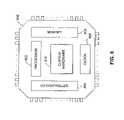
- FIG. 8is a diagram of an example system embodiment of the present invention.
- the present inventionprovides a processor, system, and method for latest producer tracking in a processor, and applications thereof.
- references to “one embodiment”, “an embodiment”, “an example embodiment”, etc.indicate that the embodiment described may include a particular feature, structure, or characteristic, but every embodiment may not necessarily include the particular feature, structure, or characteristic. Moreover, such phrases are not necessarily referring to the same embodiment. Further, when a particular feature, structure, or characteristic is described in connection with an embodiment, it is submitted that it is within the knowledge of one skilled in the art to effect such feature, structure, or characteristic in connection with other embodiments whether or not explicitly described.
- FIG. 1illustrates an example processor 100 according to an embodiment of the present invention.
- processor 100includes an instruction fetch unit 102 , an instruction cache 104 , an instruction decode and dispatch unit 106 , one or more instruction execution unit(s) 108 , a data cache 110 , an instruction graduation unit 112 , a register file 114 , and a bus interface unit 116 .
- Processor 100is preferably capable of implementing multi-threading, but need not implement multi-threading.
- multi-threadingrefers to an ability of an operating system and a processor to execute different parts of a program, called threads, simultaneously.
- Instruction fetch unit 102retrieves instructions from instruction cache 104 and provides instructions to instruction decode and dispatch unit 106 . Instructions are retrieved in program order, for example, for one or more program threads. In one embodiment, instruction fetch unit 102 includes logic for recoding compressed format instructions to a format that can be decoded and executed by processor 100 . In one embodiment, instruction fetch unit 102 includes an instruction buffer that enables instruction fetch unit 102 to hold multiple instructions for multiple program threads, which are ready for decoding, and to issue more than one instruction at a time to instruction decode and dispatch unit 106 .
- Instruction cache 104is an on-chip memory array organized as a direct associative or multi-way set associative cache such as, for example, a 2-way set associative cache or a 4-way set associative cache. In one embodiment, instruction cache 104 is virtually indexed and physically tagged, thereby allowing virtual-to-physical address translations to occur in parallel with cache accesses. Instruction cache 104 interfaces with instruction fetch unit 102 .
- Instruction decode and dispatch unit 106receives one or more instructions at a time from instruction fetch unit 102 and decodes them prior to execution. In one embodiment, instruction decode and dispatch unit 106 receives at least one instruction for each program thread being implemented during a particular clock cycle. As described herein, the number of program threads being implemented at any given point in time is variable. Decoded instructions are stored in a decoded instruction buffer and issued to instruction execution unit(s) 108 , for example, after it is determined that selected operands are available. Instructions can be dispatched from instruction decode and dispatch unit 106 to instruction execution unit(s) 108 out-of-program-order.
- Instruction execution unit(s) 108execute instructions dispatched by instruction decode and dispatch unit 106 .
- at least one instruction execution unit 108implements a load-store (RISC) architecture with single-cycle arithmetic logic unit operations (e.g., logical, shift, add, subtract, etc.).
- Other instruction execution unit(s) 108can include, for example, a floating point unit, a multiple-divide unit and/or other special purpose co-processing units. In embodiments having multiple instruction execution units 108 , one or more of the units can be implemented, for example, to operate in parallel.
- Instruction execution unit(s) 108interface with data cache 110 , register file 114 , and a results buffer (not shown).
- Data cache 110is an on-chip memory array. Data cache 110 is preferably virtually indexed and physically tagged. Data cache 110 interfaces with instruction execution unit(s) 108 .
- Register file 114represents a plurality of general purpose registers (e.g., logical/architectural state register), which are visible to a programmer. Each general purpose register is a 32-bit or a 64-bit register, for example, used for logical and/or mathematical operations and address calculations. In one embodiment, register file 114 is part of instruction execution unit(s) 108 . Optionally, one or more additional register file sets (not shown), such as shadow register file sets, can be included to minimize content switching overhead, for example, during interrupt and/or exception processing.
- Bus interface unit 116controls external interface signals for processor 100 .
- bus interface unit 116includes a collapsing write buffer used to merge write-through transactions and gather writes from uncached stores.
- Processor 100can include other features, and thus it is not limited to having just the specific features described herein.
- FIG. 2is a more detailed diagram of processor 100 . As illustrated in FIG. 2 , processor 100 performs four basic functions: instruction fetch; instruction decode and dispatch; instruction execution; and instruction graduation. These four basic functions are illustrative and not intended to limit the present invention.
- Instruction fetchbegins when a PC selector 202 selects amongst a variety of program counter values and determines a value that is used to fetch an instruction from instruction cache 104 .
- the program counter value selectedis the program counter value of a new program thread, the next sequential program counter value for an existing program thread, or a redirect program counter value associated with a branch instruction or a jump instruction.
- PC selector 202selects a new value for the next instruction to be fetched.
- tags associated with an instruction to be fetched from instruction cache 104are checked.
- the tagscontain precode bits for each instruction indicating instruction type. If these precode bits indicate that an instruction is a control transfer instruction, a branch history table is accessed and used to determine whether the control transfer instruction is likely to branch or likely not to branch.
- any compressed-format instructions that are fetchedare recoded by an optional instruction recoder 204 into a format that can be decoded and executed by processor 100 .
- processor 100implements both 16-bit instructions and 32-bit instructions
- any 16-bit compressed-format instructionsare recoded by instruction recoder 204 to form instructions having 32 bits.
- instruction recoder 204recodes both 16-bit instructions and 32-bit instructions to a format having more than 32 bits.
- instructionsare written to an instruction buffer 206 .
- this stagecan be bypassed and instructions can be dispatched directly to instruction decoder 208 .
- Instruction decode and dispatchbegins, for example, when one or more instructions are received from instruction buffer 206 and decoded by an instruction decoder 208 .
- the ability to receive instructions from instruction buffer 206may be temporarily halted until selected instructions residing within the instruction execution portion and/or instruction graduation portion of processor 100 are purged.
- Register rename map(s) located within instruction identification (ID) generator and operand renamer 210are updated and used to determine whether required source operands are available, for example, in register file 114 and/or a results buffer 218 .
- a register rename mapis a structure that holds the mapping information between programmer visible architectural state registers and internal physical registers of processor 100 .
- Register rename map(s)indicate whether data is available and where data is available.
- register renamingis used to remove instruction output dependencies and to ensure that there is a single producer of a given register in processor 100 at any given time.
- Source registersare renamed so that data is obtained from a producer at the earliest opportunity instead of waiting for the processor's architectural state to be updated.
- instruction ID generator and operand renamer 210generates and assigns an instruction ID tag to each instruction.
- An instruction ID tag assigned to an instructionis used, for example, to determine the program order of the instruction relative to other instructions.
- each instruction ID tagis a thread-specific sequentially generated value that uniquely determines the program order of instructions.
- the instruction ID tagscan be used to facilitate graduating instructions in-program-order, which were executed out-of-program-order.
- Each decoded instructionis assigned a results buffer identification value or tag by a results buffer allocater 212 .
- the results buffer identification valuedetermines the location in results buffer 218 (e.g., a physical register) where instruction execution unit(s) 108 can write calculated results for an instruction.
- the assignment of results buffer identification valuesare accomplished using a free list.
- the free listcontains as many entries as the number of entries (e.g., physical registers) that make up results buffer 218 .
- the free listcan be implemented, for example, using a bitmap. A first bit of the bitmap can be used to indicate whether the results buffer entry is either available (e.g., if the bit has a value of one) or unavailable (e.g., if the bit has a value of zero).
- results buffer completion bits associated with newly renamed instructionsare reset/cleared to indicate incomplete results.
- control logic(not shown) ensures that one program thread does not consume more than its share of results buffer entries.
- Decoded instructionsare written to a decoded instruction buffer 214 .
- An instruction dispatcher 216selects instructions residing in decoded instruction buffer 214 for dispatch to execution unit(s) 108 .
- instructionscan be dispatched for execution out-of-program-order.
- instructionsare selected and dispatched, for example, based on their age (ID tags) assuming that their operands are determined to be ready.
- Instruction execution unit(s) 108execute instructions as they are dispatched. During execution, operand data is obtained as appropriate from data cache 110 , register file 114 , and/or results buffer 218 . A multiplexer 215 and/or comparators (not shown) can be used to select data from results buffer 218 or register file 114 . A result calculated by instruction execution unit(s) 108 for a particular instruction is written to a location/entry of results buffer 218 specified by the instruction's associated results buffer identification value.
- Instruction graduation(represented in FIG. 1 by instruction graduation unit 112 ) is controlled by a graduation controller 220 .
- Graduation controller 220graduates instructions in accordance with the results buffer identification values stored in graduation buffer 224 .
- graduation controller 220updates, for example, the free list of results buffer allocater 212 to indicate a change in availability status of the graduating instruction's assigned results buffer identification value.
- processor 100includes a producer tracking circuit 302 , an operand renamer circuit 305 , and a results buffer allocater circuit 307 , which are interconnected and used to keep track of instructions that are the latest producers of values to be stored in particular registers of register file 114 .
- Producer tracking circuit 302includes a producer tracking map 303 .
- Producer tracking map 303stores producer tracking status values that are used to identify which physical registers of results buffer 218 are being used by instructions to store the latest data for particular logical register. As shown in FIG. 3 , the “1” bits stored in producer tracking map 303 for physical registers B 1 , B 3 , and B 5 indicate that the instructions writing their data to physical registers B 1 , B 3 , and B 5 are the latest producers of particular data values associated with particular logical registers.
- producer tracking map 303stores “N” one-bit producer tracking status values, where “N” is the number of physicals registers of results buffer 218 .
- the “N” one-bit valuesare indexed using buffer identification (BID) values associated with the physical registers of results buffer 218 .
- BIDbuffer identification
- INR SET/CLR logic 304is illustrated as being separate from producer tracking circuit 302 and operand renamer circuit 305 , it is to be understood that INR SET/CLR logic 304 can be implemented, for example, as a part of producer tracking circuit 302 and/or a part of operand renamer circuit 305 .
- Particular producer tracking status values stored in producer tracking map 303can be modified (e.g., set or cleared) by placing a BID value on a BID set bus or a BID clear bus.
- Operand renamer circuit 305includes a register rename map 306 .
- Register rename map 306associates particular physical registers of results buffer 218 with particular logical/architectural state registers of register file 114 .
- register rename map 306is indexed using register identification (RID) values.
- RIDregister identification
- Each RID valuerepresents one of the logical/architectural state registers of register file 114 .
- register rename map 306stores, for example, for each RID index value, a buffer identification (BID) value and an in-register (INR) status value.
- BIDbuffer identification
- INRin-register
- Each BID valuerepresents a physical register of results buffer 218 .
- the INR valuesare used to determine whether particular data values are available in a logical/architectural state register of register file 114 or in a physical register of results buffer 218 .
- AVAILdata availability
- Other valuessuch as, for example, a data availability (AVAIL) status value can also be stored as part of register rename map 306 and indexed by RID values.
- An AVAIL status valuecan be used, for example, to identify whether an instruction can be dispatched.
- operand renamer circuit 305preferably has two read address busses, two read data busses, a write address bus, and a write data bus, as illustrated in FIG. 3 .
- Operand renamer circuit 305also has an old BID value read bus that is coupled to the BID clear bus of producer tracking circuit 302 .
- Results buffer allocater circuit 307includes a results buffer free list 308 .
- Results buffer free list 308stores status values that identify which physical registers of results buffer 218 are available to store a value produced by an instruction.
- results buffer free list 308stores “N” one-bit status values, where “N” is the number of physicals registers of results buffer 218 .
- results buffer allocater circuit 307In the instruction decode and dispatch portion of the pipeline of processor 100 , instructions that produce values are assigned physical registers in which their results can be stored until instruction graduation.
- the function of results buffer allocater circuit 307is to output a BID value representing a physical register, which can be assigned to an instruction and used to store the value produced by the instruction. As shown in FIG. 3 , the BID value output by results buffer allocater circuit 307 is provided to producer tracking circuit 302 and to operand renamer circuit 305 .
- producer tracking circuit 302The operations and interactions of producer tracking circuit 302 , operand renamer circuit 305 , and results buffer allocater circuit 307 , as they relate to tracking an instruction (e.g., an ADD instruction) that is the latest producer of a data value associated with a particular logical register, will now be described in detail with references to FIGS. 3-6 .
- an instructione.g., an ADD instruction
- an instruction to be decodedis stored in a processor pipeline register 310 . This occurs in the instruction decode and dispatch portion of the pipeline of processor 100 (see FIGS. 1 and 2 ).
- Each instruction to be decodedmay potentially include a first group of bits 312 that specify a first logical/architectural state register (Source 1 ), a second group of bits 314 that specify a second logical/architectural state register (Source 2 ), and/or a third group of bits 316 that specify a third logical/architectural state register (Destination). These groups of bits, if present, are provided to operand renamer circuit 305 .
- Such an instructionincludes bits that identify the Source 1 register as register R 1 , the Source 2 register as register R 2 , and the Destination register as register R 3 .
- the bits 312 of the example ADD instructionwhich represent register R 1 , are provided to a first read address bus of operand renamer circuit 305 .
- Bits 312are used as an index into register rename map 306 .
- the bits representing register R 1index BID bits stored in register rename map 306 that represent a physical register B 3 of results buffer 218 .
- the bits representing physical register B 3are placed on a first read data bus of operand renamer circuit 305 .
- the bits representing physical register B 3are then stored as bits 322 in a second processor pipeline register 320 in a subsequent clock cycle of processor 100 .
- bits 314 of the example ADD instructionwhich represent register R 2
- Bits 314are also used as an index into register rename map 306 .
- the bits representing register R 2index BID bits stored in register rename map 306 that represent a physical register B 8 of results buffer 218 .
- the bits representing physical register B 8are placed on a second read data bus of operand renamer circuit 305 .
- the bits representing physical register B 8are then stored as bits 324 in the second pipeline register 320 in a subsequent clock cycle of processor 100 .
- the bits 316 of the example ADD instructionwhich represent register R 3 , are provided to a write address bus of operand renamer circuit 305 .
- Bits 316are used as an index into register rename map 306 .
- the bits representing register R 3index BID bits stored in register rename map 306 that represent a physical register B 5 of results buffer 218 .
- the bits representing physical register B 5are placed on an old BID bus of operand renamer circuit 305 .
- This feature of the present inventionis illustrated in more detail in FIG. 4 .
- FIG. 4is a diagram that illustrates the clearing of a producer tracking status bit of producer tracking map 303 according to an embodiment of the present invention.
- bits 316act as an index 402 into register rename map 306 of operand renamer circuit 305 .
- Index 402points to a location 404 of register rename map 306 .
- location 404stores bits that represent physical register B 5 of results buffer 218 .
- the association of physical register B 5 with logical register R 3 , together with the producer tacking status value stored at location 406 of producer tracking map 303indicates that prior to the example ADD instruction noted above, physical register B 5 was the physical register used by an instruction that was the latest producer of a particular data value associated with logical register R 3 . Because this will no longer be the case (i.e., the example ADD instruction will be the latest producer), the producer tracking status value (i.e., the “1” bit stored at location 406 of producer tracking map 303 ) must be cleared. In an embodiment, clearing the “1” bit in location 406 is accomplished by placing the bits representing physical register B 5 on the BID clear bus of producer tracking circuit 302 .
- a physical register “B 1 ”is allocated by results buffer allocater circuit 307 to hold the result of the example ADD instruction until the example ADD instruction graduates.
- bits representing physical register B 1are provided by results buffer allocater circuit 307 to pipeline buffer 320 , operand renamer circuit 305 , and producer tracking circuit 302 . As shown in FIG. 3 , these bits are stored in pipeline register 320 as bits 326 .
- FIG. 5is a diagram that illustrates how a BID value output by results buffer allocater circuit 307 is used to set a producer tracking status bit of producer tracking map 303 and to update register rename map 306 according to an embodiment of the present invention.
- the function of results buffer allocater circuit 307 and results buffer free list 308is to identify which physical registers of the results buffer are available to store a value produced by an instruction and to allocate an available physical register to an instruction that produces a value, for example, during instruction decode.
- the example ADD instructionincludes bits 316 , which indicate that the resultant value of the ADD instruction is to be written to logical/architectural state register R 3 .
- the resultant valuewill first be temporarily stored in a physical register of results buffer 218 .
- results buffer allocater circuit 307must identify a physical register that is available and communicate this information to operand renamer circuit 305 .
- results buffer free list 308show a “1 bit” associated with physical register B 0 .
- the “1 bit”indicates that physical register B 0 is currently assigned to an instruction that has not yet graduated, and thus physical register B 0 is unavailable.
- Results buffer free list 308show a “0 bit” associated with physical register B 1 .
- the “0 bit”indicates physical register B 1 is available, and thus results buffer allocater circuit 307 outputs bits (e.g., a BID value) that are used to represent/identify physical register B 1 .
- the “0 bit” associated with physical register B 1is then set to “1” to indicate that physical register B 1 is no longer available.
- the BID value output by results buffer allocater circuit 307is communicated to producer tracking circuit 302 .
- the BID valueis placed on a BID set bus, which causes a bit stored at location 502 in producer tracking map 303 to be set to a value of one.
- a value of oneindicates that the instruction associated with physical register B 1 is the latest producer of a data value (e.g., the resultant value of the ADD instruction that will be written to register R 3 of register file 114 upon graduation of the ADD instruction).
- a value of zero stored in producer tracking map 303which is indexed for example by a BID value representing physical register B 0 , indicates that any instruction associated with physical register B 0 is not the latest producer of a value.
- all of the producer tracking status values of producer tracking map 303are reset to zero.
- the BID value output by results buffer allocater circuit 307is also communicated to operand renamer circuit 305 .
- the BID valueis placed on a write data bus and written to location 404 of register rename map 305 .
- Location 404is selected for storing the BID value as a result of placing bits 316 on the write address bus of operand renamer circuit 305 .
- the INR bit stored at location 406 of register rename map 306is reset to zero to indicate that the resultant value of the ADD instruction is not yet available in register R 3 of register file 114 .
- the zero bit stored at location 406may or may not be set to one when the ADD instruction graduates.
- FIG. 6is a diagram that illustrates the updating of an INR status bit of register rename map 306 upon graduation of an instruction according to an embodiment of the present invention.
- instructionsmay be executed out-of-program-order, but all instructions graduate and update the architectural state of the processor in-program-order. This is accomplished, for example, by transferring data associated with instructions that are graduating in-program-order from the physical registers of results buffer 218 to the logical/architectural state registers of register file 114 as the instructions graduate.
- BID value 602When an instruction graduates, both the physical register and the logical/architectural state register associated with a producer instruction are known. Otherwise, the value produced by the instruction could not be transferred from the physical register of the results buffer to the logical/architectural state register of the register file.
- This informationis shown in FIG. 6 as BID value 602 and RID value 604 .
- BID value 602is placed on a BID read bus of producer tracking circuit 302
- RID value 604is placed on an RID read bus of operand renamer circuit 305 .
- a producer tracking status value stored in producer tracking map 303(e.g., at location 502 ) associated with BID value 602 is provided to INR SET/CLR logic 304 . If the producer tracking value provided to INR SET/CLR logic 304 indicates that the graduating instruction is the latest producer of a data value, INR SET/CLR logic 304 modifies the INR status value (e.g., at location 406 ) in register rename map 306 indexed by RID value 604 (e.g., index 402 ) to indicate that the data value is now available in register file 114 (e.g., in register R 3 ).
- the producer tracking value provided to INR SET/CLR logic 304indicates that the instruction associated with the graduating instruction is not the latest producer of a data value, the INR status value is not modified to indicate that the data value is available in register file 114 . This feature of the present invention is described further below with reference to FIG. 7 .
- FIG. 7is a diagram that further illustrates operation of processor 100 according to an embodiment of the present invention.
- FIG. 7shows how values stored in register rename map 306 and producer tracking map 303 are modified based on two ADD instructions over six time periods.
- the time periodseach represent multiple processor clock cycles, as can be understood by comparing for example FIG. 2 and FIG. 7 , in order to simplify the description.
- a first ADD instruction(ADD- 1 ) is fetched from instruction cache 104 .
- operand R 1is available register R 1 of register file 114 (i.e., the INR status bit equals one).
- Operand R 2is also available in register R 2 of register file 114 (i.e., the INR status bit equals one).
- the next physical register available to store the resultant value produced by instruction ADD- 1is assumed to be physical register B 1 . None of the physical registers illustrated in producer tracking map 303 are being used by an instruction that is the latest producer of a data value (i.e., all of the shown producer tracking status values are zero).
- instruction ADD- 1is undergoing decoding and operand renaming. As shown in the register rename map of FIG. 7 , for time period T 1 , no operand renaming is required for source 1 and source 2 of the instruction.
- results buffer allocater circuit 307allocates physical register B 1 to store the resultant value of instruction ADD- 1 until such time as instruction ADD- 1 graduates. How this is accomplished is shown, for example, in FIG. 5 .
- the BID value associated with physical register B 1replaces the BID value associated with physical register B 12 in register rename map 306 .
- the appropriate INR status valueis also reset to zero.
- the producer tracking status value for physical register B 1 in producer tracking map 303is set to one to indicate the instruction writing to physical register B 1 is the latest producer of the value that will be written to register R 3 .
- instruction ADD- 1is executed and generates a resultant value that is stored in physical register B 1 .
- a second ADD instruction(ADD- 2 ) is fetched from instruction cache 104 .
- operand R 1 and operand R 2are available in register R 1 and register R 2 , respectfully, of register file 114 .
- the next physical register available to store the resultant value produced by instruction ADD- 2is assumed to be physical register B 4 .
- Results buffer allocater circuit 307allocates physical register B 4 to store the resultant value of instruction ADD- 2 until such time as instruction ADD- 2 graduates.
- the BID value associated with physical register B 4replaces the BID value associated with physical register B 1 in register rename map 306 .
- the appropriate INR status valueis again reset to zero.
- the producer tracking status value for physical register B 1 in producer tracking map 303is set to zero, and the producer tracking status value for physical register B 4 is set to one to indicate that the instruction writing to physical register B 4 (i.e., ADD- 2 ) is now the latest producer of the value that will be written to register R 3 .
- instruction ADD- 1graduates during time period T 3 .
- the data value stored in physical register B 1is written to logical/architectural register R 3 .
- the BID value “B 1 ”is placed on the BID read bus of producer tracking circuit 302 . This causes the producer tracking status value “0” that is stored in producer tracking map 303 and associated with BID value “B 1 ” to be provided to INR SET/CLR logic 304 .
- INR SET/CLR logic 304Because the producer tracking status value “0” provided to INR SET/CLR logic 304 indicates that the graduating instruction (ADD- 1 ) is not the latest producer of the data value that will be written to register R 3 , INR SET/CLR logic 304 does not modify the INR status value for register R 3 in register rename map 306 to indicate that the data value is available in register file 114 . If this were to occur, subsequent instructions would use the value stored in register R 3 rather than the latest value stored in physical register B 4 by instruction ADD- 2 .
- instruction ADD- 2is executed and generates a resultant value that is stored in physical register B 4 .
- instruction ADD- 2graduates.
- the data value stored in physical register B 4is written to logical/architectural register R 3 . This is accomplished as shown, for example, in FIG. 6 .
- the BID value “B 4 ”is placed on the BID read bus of producer tracking circuit 302 . This causes the producer tracking status value “1” that is stored in producer tracking map 303 and associated with BID value “B 4 ” to be provided to INR SET/CLR logic 304 .
- INR SET/CLR logic 304modifies the INR status value for register R 3 in register rename map 306 to indicate that the data value is now available in register file 114 .
- the producer tracking status value for physical register B 4 in producer tracking map 303is set to zero.
- FIG. 8is a diagram of an example system 800 according to an embodiment of the present invention.
- System 800includes a processor 802 , a memory 804 , an input/output (I/O) controller 806 , a clock 808 , and custom hardware 810 .
- system 800is an application specific integrated circuit (ASIC) or a system on a chip (SOC).
- ASICapplication specific integrated circuit
- SOCsystem on a chip
- Processor 802is any processor that includes features of the present invention described herein and/or implements a method embodiment of the present invention.
- processor 802includes an instruction fetch unit, an instruction cache, an instruction decode and dispatch unit, one or more instruction execution unit(s), a data cache, an instruction graduation unit, a register file, and a bus interface unit similar to processor 100 described above.
- Memory 804can be any memory capable of storing instructions and/or data.
- Memory 804can include, for example, random access memory and/or read-only memory.
- I/O controller 806is used to enable components of system 800 to receive and/or send information to peripheral devices.
- I/O controller 806can include, for example, an analog-to-digital converter and/or a digital-to-analog converter.
- Clock 808is used to determine when sequential subsystems of system 800 change state. For example, each time a clock signal of clock 808 ticks, state registers of system 800 capture signals generated by combinatorial logic. In an embodiment, the clock signal of clock 808 can be varied. The clock signal can also be divided, for example, before it is provided to selected components of system 800 .
- Custom hardware 810is any hardware added to system 800 to tailor system 800 to a specific application.
- Custom hardware 810can include, for example, hardware needed to decode audio and/or video signals, accelerate graphics operations, and/or implement a smart sensor. Persons skilled in the relevant arts will understand how to implement custom hardware 810 to tailor system 800 to a specific application.
- implementationsmay also be embodied in software (e.g., computer readable code, program code, instructions and/or data disposed in any form, such as source, object or machine language) disposed, for example, in a computer usable (e.g., readable) medium configured to store the software.
- softwaree.g., computer readable code, program code, instructions and/or data disposed in any form, such as source, object or machine language
- a computer usable (e.g., readable) mediumconfigured to store the software.
- Such softwarecan enable, for example, the function, fabrication, modeling, simulation, description, and/or testing of the apparatus and methods described herein.
- thiscan be accomplished through the use of general programming languages (e.g., C, C++), GDSII databases, hardware description languages (HDL) including Verilog HDL, VHDL, SystemC Register Transfer Level (RTL) and so on, or other available programs, databases, and/or circuit (i.e., schematic) capture tools.
- Such softwarecan be disposed in any known computer usable medium including semiconductor, magnetic disk, optical disk (e.g., CD-ROM, DVD-ROM, etc.) and as a computer data signal embodied in a computer usable (e.g., readable) transmission medium (e.g., carrier wave or any other medium including digital, optical, or analog-based medium).
- the softwarecan be transmitted over communication networks including the Internet and intranets.
- the apparatus and method embodiments described hereinmay be included in a semiconductor intellectual property core, such as a microprocessor core (e.g., embodied in HDL) and transformed to hardware in the production of integrated circuits. Additionally, the apparatus and methods described herein may be embodied as a combination of hardware and software. Thus, the present invention should not be limited by any of the above-described exemplary embodiments, but should be defined only in accordance with the following claims and their equivalence.
Landscapes
- Engineering & Computer Science (AREA)
- Software Systems (AREA)
- Theoretical Computer Science (AREA)
- Physics & Mathematics (AREA)
- General Engineering & Computer Science (AREA)
- General Physics & Mathematics (AREA)
- Multimedia (AREA)
- Advance Control (AREA)
Abstract
Description
Claims (15)
Priority Applications (2)
| Application Number | Priority Date | Filing Date | Title |
|---|---|---|---|
| US11/485,959US7370178B1 (en) | 2006-07-14 | 2006-07-14 | Method for latest producer tracking in an out-of-order processor, and applications thereof |
| US12/104,308US7747840B2 (en) | 2006-07-14 | 2008-04-16 | Method for latest producer tracking in an out-of-order processor, and applications thereof |
Applications Claiming Priority (1)
| Application Number | Priority Date | Filing Date | Title |
|---|---|---|---|
| US11/485,959US7370178B1 (en) | 2006-07-14 | 2006-07-14 | Method for latest producer tracking in an out-of-order processor, and applications thereof |
Related Child Applications (1)
| Application Number | Title | Priority Date | Filing Date |
|---|---|---|---|
| US12/104,308ContinuationUS7747840B2 (en) | 2006-07-14 | 2008-04-16 | Method for latest producer tracking in an out-of-order processor, and applications thereof |
Publications (2)
| Publication Number | Publication Date |
|---|---|
| US7370178B1true US7370178B1 (en) | 2008-05-06 |
| US20080126760A1 US20080126760A1 (en) | 2008-05-29 |
Family
ID=39332473
Family Applications (2)
| Application Number | Title | Priority Date | Filing Date |
|---|---|---|---|
| US11/485,959Active2026-09-24US7370178B1 (en) | 2006-07-14 | 2006-07-14 | Method for latest producer tracking in an out-of-order processor, and applications thereof |
| US12/104,308ActiveUS7747840B2 (en) | 2006-07-14 | 2008-04-16 | Method for latest producer tracking in an out-of-order processor, and applications thereof |
Family Applications After (1)
| Application Number | Title | Priority Date | Filing Date |
|---|---|---|---|
| US12/104,308ActiveUS7747840B2 (en) | 2006-07-14 | 2008-04-16 | Method for latest producer tracking in an out-of-order processor, and applications thereof |
Country Status (1)
| Country | Link |
|---|---|
| US (2) | US7370178B1 (en) |
Cited By (5)
| Publication number | Priority date | Publication date | Assignee | Title |
|---|---|---|---|---|
| US20080189535A1 (en)* | 2007-02-01 | 2008-08-07 | Vikas Agarwal | Method and System for Dependency Tracking and Flush Recovery for an Out-Of-Order Microprocessor |
| US20080215857A1 (en)* | 2006-07-14 | 2008-09-04 | Mips Technologies, Inc. | Method For Latest Producer Tracking In An Out-Of-Order Processor, And Applications Thereof |
| US9851975B2 (en) | 2006-02-28 | 2017-12-26 | Arm Finance Overseas Limited | Compact linked-list-based multi-threaded instruction graduation buffer |
| US10296341B2 (en) | 2006-07-14 | 2019-05-21 | Arm Finance Overseas Limited | Latest producer tracking in an out-of-order processor, and applications thereof |
| CN111638911A (en)* | 2019-03-01 | 2020-09-08 | 阿里巴巴集团控股有限公司 | Processor, instruction execution equipment and method |
Citations (59)
| Publication number | Priority date | Publication date | Assignee | Title |
|---|---|---|---|---|
| US5091851A (en) | 1989-07-19 | 1992-02-25 | Hewlett-Packard Company | Fast multiple-word accesses from a multi-way set-associative cache memory |
| US5109520A (en) | 1985-02-19 | 1992-04-28 | Tektronix, Inc. | Image frame buffer access speedup by providing multiple buffer controllers each containing command FIFO buffers |
| US5325511A (en) | 1990-06-15 | 1994-06-28 | Compaq Computer Corp. | True least recently used replacement method and apparatus |
| US5493523A (en) | 1993-12-15 | 1996-02-20 | Silicon Graphics, Inc. | Mechanism and method for integer divide involving pre-alignment of the divisor relative to the dividend |
| US5493667A (en) | 1993-02-09 | 1996-02-20 | Intel Corporation | Apparatus and method for an instruction cache locking scheme |
| US5510934A (en) | 1993-12-15 | 1996-04-23 | Silicon Graphics, Inc. | Memory system including local and global caches for storing floating point and integer data |
| US5526504A (en) | 1993-12-15 | 1996-06-11 | Silicon Graphics, Inc. | Variable page size translation lookaside buffer |
| US5537538A (en) | 1993-12-15 | 1996-07-16 | Silicon Graphics, Inc. | Debug mode for a superscalar RISC processor |
| US5546545A (en) | 1994-12-09 | 1996-08-13 | International Business Machines Corporation | Rotating priority selection logic circuit |
| US5568630A (en) | 1991-03-11 | 1996-10-22 | Silicon Graphics, Inc. | Backward-compatible computer architecture with extended word size and address space |
| US5572704A (en) | 1993-12-15 | 1996-11-05 | Silicon Graphics, Inc. | System and method for controlling split-level caches in a multi-processor system including data loss and deadlock prevention schemes |
| US5586278A (en) | 1994-03-01 | 1996-12-17 | Intel Corporation | Method and apparatus for state recovery following branch misprediction in an out-of-order microprocessor |
| US5604909A (en) | 1993-12-15 | 1997-02-18 | Silicon Graphics Computer Systems, Inc. | Apparatus for processing instructions in a computing system |
| US5606683A (en) | 1994-01-28 | 1997-02-25 | Quantum Effect Design, Inc. | Structure and method for virtual-to-physical address translation in a translation lookaside buffer |
| US5670898A (en) | 1995-11-22 | 1997-09-23 | Silicon Graphics, Inc. | Low-power, compact digital logic topology that facilitates large fan-in and high-speed circuit performance |
| US5734881A (en) | 1995-12-15 | 1998-03-31 | Cyrix Corporation | Detecting short branches in a prefetch buffer using target location information in a branch target cache |
| US5740402A (en) | 1993-12-15 | 1998-04-14 | Silicon Graphics, Inc. | Conflict resolution in interleaved memory systems with multiple parallel accesses |
| US5758112A (en) | 1994-10-14 | 1998-05-26 | Silicon Graphics, Inc. | Pipeline processor with enhanced method and apparatus for restoring register-renaming information in the event of a branch misprediction |
| US5765037A (en) | 1985-10-31 | 1998-06-09 | Biax Corporation | System for executing instructions with delayed firing times |
| US5764999A (en) | 1995-10-10 | 1998-06-09 | Cyrix Corporation | Enhanced system management mode with nesting |
| US5781753A (en) | 1989-02-24 | 1998-07-14 | Advanced Micro Devices, Inc. | Semi-autonomous RISC pipelines for overlapped execution of RISC-like instructions within the multiple superscalar execution units of a processor having distributed pipeline control for speculative and out-of-order execution of complex instructions |
| US5784584A (en) | 1989-08-03 | 1998-07-21 | Patriot Scientific Corporation | High performance microprocessor using instructions that operate within instruction groups |
| US5799165A (en) | 1996-01-26 | 1998-08-25 | Advanced Micro Devices, Inc. | Out-of-order processing that removes an issued operation from an execution pipeline upon determining that the operation would cause a lengthy pipeline delay |
| US5802339A (en) | 1994-11-15 | 1998-09-01 | Advanced Micro Devices | Pipeline throughput via parallel out-of-order execution of adds and moves in a supplemental integer execution unit |
| US5802386A (en) | 1996-11-19 | 1998-09-01 | International Business Machines Corporation | Latency-based scheduling of instructions in a superscalar processor |
| GB2322718A (en) | 1996-12-09 | 1998-09-02 | Ibm | Dynamic classification and dispatch of instructions out of order |
| US5809326A (en) | 1995-09-25 | 1998-09-15 | Kabushiki Kaisha Toshiba | Signal processor and method of operating a signal processor |
| US5881257A (en) | 1996-09-23 | 1999-03-09 | Arm Limited | Data processing system register control |
| US5884061A (en) | 1994-10-24 | 1999-03-16 | International Business Machines Corporation | Apparatus to perform source operand dependency analysis perform register renaming and provide rapid pipeline recovery for a microprocessor capable of issuing and executing multiple instructions out-of-order in a single processor cycle |
| US5961629A (en) | 1991-07-08 | 1999-10-05 | Seiko Epson Corporation | High performance, superscalar-based computer system with out-of-order instruction execution |
| US5966734A (en) | 1996-10-18 | 1999-10-12 | Samsung Electronics Co., Ltd. | Resizable and relocatable memory scratch pad as a cache slice |
| US6044478A (en) | 1997-05-30 | 2000-03-28 | National Semiconductor Corporation | Cache with finely granular locked-down regions |
| US6076159A (en) | 1997-09-12 | 2000-06-13 | Siemens Aktiengesellschaft | Execution of a loop instructing in a loop pipeline after detection of a first occurrence of the loop instruction in an integer pipeline |
| US6079014A (en) | 1993-12-02 | 2000-06-20 | Intel Corporation | Processor that redirects an instruction fetch pipeline immediately upon detection of a mispredicted branch while committing prior instructions to an architectural state |
| US6085315A (en) | 1997-09-12 | 2000-07-04 | Siemens Aktiengesellschaft | Data processing device with loop pipeline |
| US6216200B1 (en) | 1994-10-14 | 2001-04-10 | Mips Technologies, Inc. | Address queue |
| US6223278B1 (en) | 1998-11-05 | 2001-04-24 | Intel Corporation | Method and apparatus for floating point (FP) status word handling in an out-of-order (000) Processor Pipeline |
| US6249862B1 (en) | 1996-05-17 | 2001-06-19 | Advanced Micro Devices, Inc. | Dependency table for reducing dependency checking hardware |
| US6266755B1 (en) | 1994-10-14 | 2001-07-24 | Mips Technologies, Inc. | Translation lookaside buffer with virtual address conflict prevention |
| US6298438B1 (en) | 1996-12-02 | 2001-10-02 | Advanced Micro Devices, Inc. | System and method for conditional moving an operand from a source register to destination register |
| US6308252B1 (en) | 1999-02-04 | 2001-10-23 | Kabushiki Kaisha Toshiba | Processor method and apparatus for performing single operand operation and multiple parallel operand operation |
| US6393550B1 (en) | 1993-12-30 | 2002-05-21 | Intel Corporation | Method and apparatus for pipeline streamlining where resources are immediate or certainly retired |
| US6430655B1 (en) | 2000-01-31 | 2002-08-06 | Mips Technologies, Inc. | Scratchpad RAM memory accessible in parallel to a primary cache |
| WO2002082278A1 (en) | 2001-04-04 | 2002-10-17 | Mips Technologies, Inc. | Cache write bypass system |
| US6473837B1 (en) | 1999-05-18 | 2002-10-29 | Advanced Micro Devices, Inc. | Snoop resynchronization mechanism to preserve read ordering |
| US6477639B1 (en) | 1999-10-01 | 2002-11-05 | Hitachi, Ltd. | Branch instruction mechanism for processor |
| US6505285B1 (en) | 2000-06-26 | 2003-01-07 | Ncr Corporation | Scratch segment subsystem for a parallel processing database system |
| US6546477B1 (en) | 1999-09-20 | 2003-04-08 | Texas Instruments Incorporated | Memory management in embedded systems with dynamic object instantiation |
| US6557127B1 (en) | 2000-02-28 | 2003-04-29 | Cadence Design Systems, Inc. | Method and apparatus for testing multi-port memories |
| US6594728B1 (en) | 1994-10-14 | 2003-07-15 | Mips Technologies, Inc. | Cache memory with dual-way arrays and multiplexed parallel output |
| US6757817B1 (en) | 2000-05-19 | 2004-06-29 | Intel Corporation | Apparatus having a cache and a loop buffer |
| US6760835B1 (en) | 2000-11-22 | 2004-07-06 | Lsi Logic Corporation | Instruction branch mispredict streaming |
| US20040193858A1 (en) | 2003-03-24 | 2004-09-30 | Infineon Technologies North America Corp. | Zero-overhead loop operation in microprocessor having instruction buffer |
| US6836833B1 (en) | 2002-10-22 | 2004-12-28 | Mips Technologies, Inc. | Apparatus and method for discovering a scratch pad memory configuration |
| US6915395B1 (en) | 2000-05-03 | 2005-07-05 | Sun Microsystems, Inc. | Active address content addressable memory |
| US7032226B1 (en) | 2000-06-30 | 2006-04-18 | Mips Technologies, Inc. | Methods and apparatus for managing a buffer of events in the background |
| US20060095732A1 (en) | 2004-08-30 | 2006-05-04 | Tran Thang M | Processes, circuits, devices, and systems for scoreboard and other processor improvements |
| US20060149904A1 (en) | 1995-03-24 | 2006-07-06 | Silicon Graphics, Inc. | Prefetching hints |
| US20060259747A1 (en) | 2003-07-29 | 2006-11-16 | Stretch, Inc. | Long instruction word processing with instruction extensions |
Family Cites Families (12)
| Publication number | Priority date | Publication date | Assignee | Title |
|---|---|---|---|---|
| US679014A (en)* | 1900-09-27 | 1901-07-23 | Jerome Odell Boger | Plow. |
| US5452426A (en)* | 1994-01-04 | 1995-09-19 | Intel Corporation | Coordinating speculative and committed state register source data and immediate source data in a processor |
| US5675759A (en)* | 1995-03-03 | 1997-10-07 | Shebanow; Michael C. | Method and apparatus for register management using issue sequence prior physical register and register association validity information |
| US6148233A (en)* | 1997-03-07 | 2000-11-14 | Cardiac Science, Inc. | Defibrillation system having segmented electrodes |
| US5974535A (en) | 1997-05-09 | 1999-10-26 | International Business Machines Corporation | Method and system in data processing system of permitting concurrent processing of instructions of a particular type |
| US7401205B1 (en) | 1999-08-13 | 2008-07-15 | Mips Technologies, Inc. | High performance RISC instruction set digital signal processor having circular buffer and looping controls |
| US6395550B1 (en)* | 2000-01-10 | 2002-05-28 | Corgentech, Inc. | Method and apparatus for tissue treatment |
| US7502876B1 (en) | 2000-06-23 | 2009-03-10 | Mips Technologies, Inc. | Background memory manager that determines if data structures fits in memory with memory state transactions map |
| US7055021B2 (en) | 2002-02-05 | 2006-05-30 | Sun Microsystems, Inc. | Out-of-order processor that reduces mis-speculation using a replay scoreboard |
| US20040128483A1 (en) | 2002-12-31 | 2004-07-01 | Intel Corporation | Fuser renamer apparatus, systems, and methods |
| US7370178B1 (en) | 2006-07-14 | 2008-05-06 | Mips Technologies, Inc. | Method for latest producer tracking in an out-of-order processor, and applications thereof |
| US20080016326A1 (en) | 2006-07-14 | 2008-01-17 | Mips Technologies, Inc. | Latest producer tracking in an out-of-order processor, and applications thereof |
- 2006
- 2006-07-14USUS11/485,959patent/US7370178B1/enactiveActive
- 2008
- 2008-04-16USUS12/104,308patent/US7747840B2/enactiveActive
Patent Citations (66)
| Publication number | Priority date | Publication date | Assignee | Title |
|---|---|---|---|---|
| US5109520A (en) | 1985-02-19 | 1992-04-28 | Tektronix, Inc. | Image frame buffer access speedup by providing multiple buffer controllers each containing command FIFO buffers |
| US5765037A (en) | 1985-10-31 | 1998-06-09 | Biax Corporation | System for executing instructions with delayed firing times |
| US5781753A (en) | 1989-02-24 | 1998-07-14 | Advanced Micro Devices, Inc. | Semi-autonomous RISC pipelines for overlapped execution of RISC-like instructions within the multiple superscalar execution units of a processor having distributed pipeline control for speculative and out-of-order execution of complex instructions |
| US5091851A (en) | 1989-07-19 | 1992-02-25 | Hewlett-Packard Company | Fast multiple-word accesses from a multi-way set-associative cache memory |
| US5809336A (en) | 1989-08-03 | 1998-09-15 | Patriot Scientific Corporation | High performance microprocessor having variable speed system clock |
| US6598148B1 (en) | 1989-08-03 | 2003-07-22 | Patriot Scientific Corporation | High performance microprocessor having variable speed system clock |
| US5784584A (en) | 1989-08-03 | 1998-07-21 | Patriot Scientific Corporation | High performance microprocessor using instructions that operate within instruction groups |
| US5325511A (en) | 1990-06-15 | 1994-06-28 | Compaq Computer Corp. | True least recently used replacement method and apparatus |
| US5568630A (en) | 1991-03-11 | 1996-10-22 | Silicon Graphics, Inc. | Backward-compatible computer architecture with extended word size and address space |
| US5961629A (en) | 1991-07-08 | 1999-10-05 | Seiko Epson Corporation | High performance, superscalar-based computer system with out-of-order instruction execution |
| US5493667A (en) | 1993-02-09 | 1996-02-20 | Intel Corporation | Apparatus and method for an instruction cache locking scheme |
| US6079014A (en) | 1993-12-02 | 2000-06-20 | Intel Corporation | Processor that redirects an instruction fetch pipeline immediately upon detection of a mispredicted branch while committing prior instructions to an architectural state |
| US5493523A (en) | 1993-12-15 | 1996-02-20 | Silicon Graphics, Inc. | Mechanism and method for integer divide involving pre-alignment of the divisor relative to the dividend |
| US5537538A (en) | 1993-12-15 | 1996-07-16 | Silicon Graphics, Inc. | Debug mode for a superscalar RISC processor |
| US5632025A (en) | 1993-12-15 | 1997-05-20 | Silicon Graphics, Inc. | Method for preventing multi-level cache system deadlock in a multi-processor system |
| US6247124B1 (en) | 1993-12-15 | 2001-06-12 | Mips Technologies, Inc. | Branch prediction entry with target line index calculated using relative position of second operation of two step branch operation in a line of instructions |
| US5572704A (en) | 1993-12-15 | 1996-11-05 | Silicon Graphics, Inc. | System and method for controlling split-level caches in a multi-processor system including data loss and deadlock prevention schemes |
| US5740402A (en) | 1993-12-15 | 1998-04-14 | Silicon Graphics, Inc. | Conflict resolution in interleaved memory systems with multiple parallel accesses |
| US5604909A (en) | 1993-12-15 | 1997-02-18 | Silicon Graphics Computer Systems, Inc. | Apparatus for processing instructions in a computing system |
| US6691221B2 (en) | 1993-12-15 | 2004-02-10 | Mips Technologies, Inc. | Loading previously dispatched slots in multiple instruction dispatch buffer before dispatching remaining slots for parallel execution |
| US5954815A (en) | 1993-12-15 | 1999-09-21 | Silicon Graphics, Inc. | Invalidating instructions in fetched instruction blocks upon predicted two-step branch operations with second operation relative target address |
| US5526504A (en) | 1993-12-15 | 1996-06-11 | Silicon Graphics, Inc. | Variable page size translation lookaside buffer |
| US5510934A (en) | 1993-12-15 | 1996-04-23 | Silicon Graphics, Inc. | Memory system including local and global caches for storing floating point and integer data |
| US6393550B1 (en) | 1993-12-30 | 2002-05-21 | Intel Corporation | Method and apparatus for pipeline streamlining where resources are immediate or certainly retired |
| US5606683A (en) | 1994-01-28 | 1997-02-25 | Quantum Effect Design, Inc. | Structure and method for virtual-to-physical address translation in a translation lookaside buffer |
| US5586278A (en) | 1994-03-01 | 1996-12-17 | Intel Corporation | Method and apparatus for state recovery following branch misprediction in an out-of-order microprocessor |
| US5758112A (en) | 1994-10-14 | 1998-05-26 | Silicon Graphics, Inc. | Pipeline processor with enhanced method and apparatus for restoring register-renaming information in the event of a branch misprediction |
| US6594728B1 (en) | 1994-10-14 | 2003-07-15 | Mips Technologies, Inc. | Cache memory with dual-way arrays and multiplexed parallel output |
| US6266755B1 (en) | 1994-10-14 | 2001-07-24 | Mips Technologies, Inc. | Translation lookaside buffer with virtual address conflict prevention |
| US6216200B1 (en) | 1994-10-14 | 2001-04-10 | Mips Technologies, Inc. | Address queue |
| US5884061A (en) | 1994-10-24 | 1999-03-16 | International Business Machines Corporation | Apparatus to perform source operand dependency analysis perform register renaming and provide rapid pipeline recovery for a microprocessor capable of issuing and executing multiple instructions out-of-order in a single processor cycle |
| US5802339A (en) | 1994-11-15 | 1998-09-01 | Advanced Micro Devices | Pipeline throughput via parallel out-of-order execution of adds and moves in a supplemental integer execution unit |
| US5546545A (en) | 1994-12-09 | 1996-08-13 | International Business Machines Corporation | Rotating priority selection logic circuit |
| US20060149904A1 (en) | 1995-03-24 | 2006-07-06 | Silicon Graphics, Inc. | Prefetching hints |
| US5809326A (en) | 1995-09-25 | 1998-09-15 | Kabushiki Kaisha Toshiba | Signal processor and method of operating a signal processor |
| US5764999A (en) | 1995-10-10 | 1998-06-09 | Cyrix Corporation | Enhanced system management mode with nesting |
| US5670898A (en) | 1995-11-22 | 1997-09-23 | Silicon Graphics, Inc. | Low-power, compact digital logic topology that facilitates large fan-in and high-speed circuit performance |
| US5734881A (en) | 1995-12-15 | 1998-03-31 | Cyrix Corporation | Detecting short branches in a prefetch buffer using target location information in a branch target cache |
| US5799165A (en) | 1996-01-26 | 1998-08-25 | Advanced Micro Devices, Inc. | Out-of-order processing that removes an issued operation from an execution pipeline upon determining that the operation would cause a lengthy pipeline delay |
| US6249862B1 (en) | 1996-05-17 | 2001-06-19 | Advanced Micro Devices, Inc. | Dependency table for reducing dependency checking hardware |
| US5881257A (en) | 1996-09-23 | 1999-03-09 | Arm Limited | Data processing system register control |
| US5966734A (en) | 1996-10-18 | 1999-10-12 | Samsung Electronics Co., Ltd. | Resizable and relocatable memory scratch pad as a cache slice |
| US5802386A (en) | 1996-11-19 | 1998-09-01 | International Business Machines Corporation | Latency-based scheduling of instructions in a superscalar processor |
| US6298438B1 (en) | 1996-12-02 | 2001-10-02 | Advanced Micro Devices, Inc. | System and method for conditional moving an operand from a source register to destination register |
| GB2322718A (en) | 1996-12-09 | 1998-09-02 | Ibm | Dynamic classification and dispatch of instructions out of order |
| US6044478A (en) | 1997-05-30 | 2000-03-28 | National Semiconductor Corporation | Cache with finely granular locked-down regions |
| US6085315A (en) | 1997-09-12 | 2000-07-04 | Siemens Aktiengesellschaft | Data processing device with loop pipeline |
| US6076159A (en) | 1997-09-12 | 2000-06-13 | Siemens Aktiengesellschaft | Execution of a loop instructing in a loop pipeline after detection of a first occurrence of the loop instruction in an integer pipeline |
| US6223278B1 (en) | 1998-11-05 | 2001-04-24 | Intel Corporation | Method and apparatus for floating point (FP) status word handling in an out-of-order (000) Processor Pipeline |
| US6308252B1 (en) | 1999-02-04 | 2001-10-23 | Kabushiki Kaisha Toshiba | Processor method and apparatus for performing single operand operation and multiple parallel operand operation |
| US6473837B1 (en) | 1999-05-18 | 2002-10-29 | Advanced Micro Devices, Inc. | Snoop resynchronization mechanism to preserve read ordering |
| US6546477B1 (en) | 1999-09-20 | 2003-04-08 | Texas Instruments Incorporated | Memory management in embedded systems with dynamic object instantiation |
| US6477639B1 (en) | 1999-10-01 | 2002-11-05 | Hitachi, Ltd. | Branch instruction mechanism for processor |
| US6430655B1 (en) | 2000-01-31 | 2002-08-06 | Mips Technologies, Inc. | Scratchpad RAM memory accessible in parallel to a primary cache |
| US6557127B1 (en) | 2000-02-28 | 2003-04-29 | Cadence Design Systems, Inc. | Method and apparatus for testing multi-port memories |
| US6915395B1 (en) | 2000-05-03 | 2005-07-05 | Sun Microsystems, Inc. | Active address content addressable memory |
| US6757817B1 (en) | 2000-05-19 | 2004-06-29 | Intel Corporation | Apparatus having a cache and a loop buffer |
| US6505285B1 (en) | 2000-06-26 | 2003-01-07 | Ncr Corporation | Scratch segment subsystem for a parallel processing database system |
| US7032226B1 (en) | 2000-06-30 | 2006-04-18 | Mips Technologies, Inc. | Methods and apparatus for managing a buffer of events in the background |
| US6760835B1 (en) | 2000-11-22 | 2004-07-06 | Lsi Logic Corporation | Instruction branch mispredict streaming |
| WO2002082278A1 (en) | 2001-04-04 | 2002-10-17 | Mips Technologies, Inc. | Cache write bypass system |
| US20050102483A1 (en) | 2002-10-22 | 2005-05-12 | Kinter Ryan C. | Apparatus and method for discovering a scratch pad memory configuration |
| US6836833B1 (en) | 2002-10-22 | 2004-12-28 | Mips Technologies, Inc. | Apparatus and method for discovering a scratch pad memory configuration |
| US20040193858A1 (en) | 2003-03-24 | 2004-09-30 | Infineon Technologies North America Corp. | Zero-overhead loop operation in microprocessor having instruction buffer |
| US20060259747A1 (en) | 2003-07-29 | 2006-11-16 | Stretch, Inc. | Long instruction word processing with instruction extensions |
| US20060095732A1 (en) | 2004-08-30 | 2006-05-04 | Tran Thang M | Processes, circuits, devices, and systems for scoreboard and other processor improvements |
Non-Patent Citations (52)
| Title |
|---|
| ADSP-21535 Blackfin(TM) DSP Brochure, Analog Devices, Inc., 4 pages. (2001). |
| Andes R10000 User's Manual, Revision 2.0, MIPS Technologies, Inc., Entire Text (Sep. 19, 1996). |
| Arvind, A. and Maessen, J.-W., "Memory Model = Instruction Reordering + Store Atomicity," ACM SIGARCH Computer Architecture News, vol. 34, Issue 2, pp. 29-40 (May 2006). |
| Banakar, R. et al., "Scratchpad Memory: A Design Alternative for Cache On-chip memory in Embedded Systems," Proceedings of CODES'02, ACM, Estes Park, Colorado, pp. 73-78 (May 2002). |
| Bellas, N. et al., "Architectural and Compiler Techniques for Energy Reduction in High-Performance Microprocessors," IEEE Trans. on Very Large Scale Integration (VLSI) Systems, vol. 8, No. 3, pp. 317-326 (Jun. 2000). |
| Bird, P.L. et al., "The Effectiveness of Decoupling," Proceedings of the 7th Int'l Conference on Supercomputing, pp. 47-56, ACM Press, New York, NY (1993). |
| Bratt, J.P. et al., US. Appl. No. 08/168,094, filed Dec. 15, 1993, entitled "Superscalar Microprocessor Instruction Pipeline Including Instruction Dispatching and Kill Control". |
| Buti, T.N. et al., "Organization and implementation of the register-renaming mapper for out-of-order IBM POWER4 processors," IBM J. Res. & Dev. 49(1):167-188, International Business Machines Corporation (Jan. 2005). |
| Cotterell, S. and Vahid, F., "Tuning of Loop Cache Architecture to Programs in Embedded System Design," ISSS'02, 6 pages (Oct. 2002). |
| Courtright, D., "Introducing: The MIPS32(TM) 4Kc(TM) and MIPS32(TM) 4Kp(TM) Processor Cores 'Jade'," paper copy of slide presentation distributed at the Embedded Microprocessor Forum, pp. 1-25 (May 1999). |
| Dally, W.J. et al., U.S. Appl. No. 09/637,500, filed Aug. 11, 2000, entitled "High Performance RISC Instruction Set Digital Signal Processor Having Circular Buffer and Looping Controls". |
| De Vries, H., Understanding the detailed Architecture of AMD's 64 bit Core, 85 pages, printed Oct. 16, 2007 from http://chip-architect.com/news/2003<SUB>-</SUB>09<SUB>-</SUB>21<SUB>-</SUB>Detailed<SUB>-</SUB>Architecture<SUB>-</SUB>of<SUB>-</SUB>AMDs<SUB>-</SUB>64bit<SUB>-</SUB>Core.html (Sep. 21, 2003). |
| Flynn et al., "Using Simple Tools to Evaluate Complex Architectural Trade-Offs," IEEE Micro, pp. 67-75 (Jul.-Aug. 2000). |
| Fukuoka, K. et al., "Leakage Power Reduction for Clock Gating Scheme on PD-SOI," IEEE Computer Society Int'l Symp. on Circuits and Systems, pp. 613-616 (2004). |
| Goodman, J.R. et al., "PIPE: A VLSI Decoupled Architecture," ACM SIGARCH Computer Architecture News, pp. 20-27, ACM Press, New York, NY (Jun. 1985). |
| Gwennap, L., "MIPS R10000 Uses Decoupled Architecture," Microprocessor Report, vol. 8, No. 14, pp. 1-5 (Oct. 24, 1994). |
| Gwennap, L., "MIPS R12000 to Hit 300 MHz," Microprocessor Report, vol. 11, No. 13, pp. 1-4 (Oct. 6, 1997). |
| Gwennap, L., "MIPS Roadmap Focuses on Bandwidth," Microprocessor Report, pp. 1-3 (May 12, 1997). |
| Gwennap, L., "SGI Provides Overview of TFP CPU," Microprocessor Report, vol. 7, No. 2, pp. 1-2 (Feb. 15, 1993). |
| Gwennap, L., "TFP Designed for Tremendous Floating Point," Microprocessor Report, vol. 7, No. 11, pp. 1-5 (Aug. 23, 1993). |
| Intel Architecture Software Developer's Manual- vol. 2: Instruction Set Reference, Intel. Corporation, pp. 3-278 and 3-279 (1997). |
| Intel Architecture Software Developer's Manual, vol. 1-3, pp. 2-7, 2-10, 2-11, 2-12, 3-320, 9-16, A-10, and A-20 (1999). |
| Intel(R) StrongARM(R) SA-1100 Microprocessor Developer's Manual, Intel. Corporation, pp. i-xix, 1-1 through 1-7, 2-1 through 2-8, and 6-1 through 6-7 (Aug. 1999). |
| Kandemir, M. et al., "Dynamic Management of Scratch-Pad Memory Space," Proceedings of the 38<SUP>th </SUP>Design Automation Conference, ACM, Las Vegas, Nevada, pp. 690-695 (Jun. 2001). |
| Kandemir, M. et al., "Exploiting Scratch Pad Memory Using Presburger Formulas," Proceedings of ISSS '01, ACM, Montreal, Quebec, Canada, pp. 7-12 (Oct. 2001). |
| Kandemir, M. et al., "Exploiting Shared Scratch Pad Memory Space in Embedded Multiprocessor Systems," Proceedings of the 39<SUP>th </SUP>Design Automation Conference, ACM, New Orleans, Louisiana, pp. 219-224 (Jun. 2002). |
| Kiyohara, T. et al., "Register Connection: A New Approach to Adding Registers into Instruction Set Architectures," Int'l Conf. on Computer Architecture-Proc. of the 20th Annual Int'l. Symp. on Computer Architecture, San Diego, CA, pp. 247-256 (1993). |
| Krewell, K., "Intel Looks To Core For Success", Microprocessor Report, vol. 20, pp. 1, 4, 5 and 6 (Mar. 2006). |
| Lee, L.H. et al., "Instruction Fetch Energy Reduction Using Loop Caches For Embedded Applications with Small Tight Loops," ISLPED'99, pp. 267-269 (1999). |
| Lipasti, M. et al., "Physical Register Inlining," at <http://www.ece.wisc.edu/~pharm/papers/isca2004<SUB>-</SUB>egunadi.pdf>, 11 pages (retrieved Jun. 12, 2006). |
| Merten, M.C. et al., "Modulo Schedule Buffers", IEEE, pp. 138-149 (Dec. 2001). |
| MIPS R10000 Microprocessor User's Manual, Version 2.0, MIPS Technologies, Inc., 424 pages (Jan. 29, 1997). |
| Nass, R., "Latest DSPs Poised to Drive 3G Revolution," Portable Design 8(9):26, 27, 28, 32, and 34, PennWell Corporation, Fair Lawn, New Jersey (Sep. 2001). |
| Nemirovsky, M. et al., U.S. Appl. No. 09/602,279, filed Jun. 23, 2000, entitled "Methods and Apparatus for Background Memory Management". |
| Osborne, M. et al., "Superscalar Pipeline Architectures," Slide Presentation, 37 pages, downloaded Jun. 19, 2007 from http://www.academic.marist.edu/~jzbv/architecture/projects2004/SuperscalarArchitectures.ppt (Apr. 19, 2004). |
| Panda, P. et al., "Data Memory Organization and Optimizations in Application-Specific Systems," IEEE Design & Test of Computers, IEEE, pp. 56-68 (May 2001). |
| Panda, P. et al., "Efficient Utilization of Scratch-Pad Memory in Embedded Processor Applications," Proceedings of the European Design & Test Conference ED&TC 97, IEEE, Paris France, pp. 7-11 (Mar. 1997). |
| Peng, M. and Azgomi, S., "Content-Addressable memory (CAM) and its network applications," at <http://www.eetasia.com/ARTICLES/2000MAY/2000MAY03<SUB>-</SUB>MEM<SUB>-</SUB>NTEK<SUB>-</SUB>TAC.PDF>, 3 pages (retrieved Jun. 12, 2006). |
| Pierce, J. and Mudge, T., "Wrong-Path Instruction Prefetching," IEEE Computer Society 29th Int'l Symp. on Microarchitecture, pp. 165-175 (1996). |
| Price, C., MIPS R10000 MIPS IV ISA Manual: Andes, Revision 3.2, MIPS Technologies, Inc., 323 pages (Sep. 1995). |
| Rhodes, S., MIPS R8000 Microprocessor Chip Set User's Manual, Revision 3.0, Silicon Graphics, Inc., 352 pages (Jul. 1994). |
| Schmidt, D.C., "Transparently Parameterizing Synchronization into a Concurrent Distributed Application: A Case Study of C++ Design Evolution," C++ Report, SIGS Publications, vol. 6, No. 3, 10 pages (Jul.-Aug. 1994). |
| Smith, J.E. et al., "The ZS-1 Central Processor," Proceedings of the Second Int'l Conference on Architectural Support for Programming Languages and Operating Systems, pp. 199-204, IEEE Computer Society Press, Los Alamitos, CA (1987). |
| Smith, J.E., "Retrospective: Decoupled Access/Execute Computer Architectures," 25 Years of the international Symposia on Computer Architecture(Selected Papers), pp. 27-28, ACM Press, New York, NY (Jun. 1998). |
| Solomon, B. et al., "Micro-Operation Cache: A Power Aware Frontend for Variable Instruction Length ISA," Symp. on Low Power Electronics and Design, pp. 4-9 (Aug. 2001). |
| SPARC64 V Processor For UNIX Server, Revision 1.0, Fujitsu Limited, 24 pages (Aug. 2004). |
| Sung, M. et al., "Multithreading Decoupled Architectures for Complexity-Effective General Purpose Computing," ACM SIGARCH Computer Architecture News, vol. 29-Issue 5, pp. 56-61, ACM Press, New York, NY (Dec. 2001). |
| Svendsen, K. et al., U.S. Appl. No. 11/485,960, filed Jul. 14, 2006, entitled "Latest Producer Tracking in an Out-of-Order Processor, and Applications Thereof". |
| Taylor, M., The Raw Prototype Design Document, Dept. of Electrical Engineering and Computer Science-Massachusetts Institute of Technology, pp. 1, 5, 6, 10, and 53 (Nov. 1999). |
| V<SUB>R</SUB>Series(TM) User's Manual:V<SUB>R</SUB>10000(TM) Microprocessor, Version 1.0, NEC, Entire Text (Nov. 1995). |
| Watts, C. et al., "ARM Intelligent Energy Manager Future Evolution," paper copy of slide presentation distributed at the ARM Developers' Conference '04, 34 sheets (Oct. 2004). |
| Yeager, K.C., "The MIPS R10000 Superscalar Microprocessor," IEEE Micro, pp. 28-40 (1996). |
Cited By (8)
| Publication number | Priority date | Publication date | Assignee | Title |
|---|---|---|---|---|
| US9851975B2 (en) | 2006-02-28 | 2017-12-26 | Arm Finance Overseas Limited | Compact linked-list-based multi-threaded instruction graduation buffer |
| US10691462B2 (en) | 2006-02-28 | 2020-06-23 | Arm Finance Overseas Limited | Compact linked-list-based multi-threaded instruction graduation buffer |
| US20080215857A1 (en)* | 2006-07-14 | 2008-09-04 | Mips Technologies, Inc. | Method For Latest Producer Tracking In An Out-Of-Order Processor, And Applications Thereof |
| US7747840B2 (en) | 2006-07-14 | 2010-06-29 | Mips Technologies, Inc. | Method for latest producer tracking in an out-of-order processor, and applications thereof |
| US10296341B2 (en) | 2006-07-14 | 2019-05-21 | Arm Finance Overseas Limited | Latest producer tracking in an out-of-order processor, and applications thereof |
| US20080189535A1 (en)* | 2007-02-01 | 2008-08-07 | Vikas Agarwal | Method and System for Dependency Tracking and Flush Recovery for an Out-Of-Order Microprocessor |
| US7660971B2 (en)* | 2007-02-01 | 2010-02-09 | International Business Machines Corporation | Method and system for dependency tracking and flush recovery for an out-of-order microprocessor |
| CN111638911A (en)* | 2019-03-01 | 2020-09-08 | 阿里巴巴集团控股有限公司 | Processor, instruction execution equipment and method |
Also Published As
| Publication number | Publication date |
|---|---|
| US7747840B2 (en) | 2010-06-29 |
| US20080126760A1 (en) | 2008-05-29 |
| US20080215857A1 (en) | 2008-09-04 |
Similar Documents
| Publication | Publication Date | Title |
|---|---|---|
| US8032734B2 (en) | Coprocessor load data queue for interfacing an out-of-order execution unit with an in-order coprocessor | |
| US10768939B2 (en) | Load/store unit for a processor, and applications thereof | |
| US7647475B2 (en) | System for synchronizing an in-order co-processor with an out-of-order processor using a co-processor interface store data queue | |
| US10430340B2 (en) | Data cache virtual hint way prediction, and applications thereof | |
| US10691462B2 (en) | Compact linked-list-based multi-threaded instruction graduation buffer | |
| CN106648554B (en) | System, method and apparatus for improving throughput of contiguous transactional memory regions | |
| US10296341B2 (en) | Latest producer tracking in an out-of-order processor, and applications thereof | |
| JP7156776B2 (en) | System and method for merging partial write results during retirement phase | |
| US20130305022A1 (en) | Speeding Up Younger Store Instruction Execution after a Sync Instruction | |
| US8078846B2 (en) | Conditional move instruction formed into one decoded instruction to be graduated and another decoded instruction to be invalidated | |
| US7747840B2 (en) | Method for latest producer tracking in an out-of-order processor, and applications thereof | |
| US20080082793A1 (en) | Detection and prevention of write-after-write hazards, and applications thereof | |
| CN101535947A (en) | Twice issued conditional move instruction, and applications thereof |
Legal Events
| Date | Code | Title | Description |
|---|---|---|---|
| AS | Assignment | Owner name:MIPS TECHNOLOGIES, INC., CALIFORNIA Free format text:ASSIGNMENT OF ASSIGNORS INTEREST;ASSIGNORS:SVENDSEN, KJELD;JIANG, XING YU;REEL/FRAME:018057/0982 Effective date:20060713 | |
| AS | Assignment | Owner name:JEFFERIES FINANCE LLC, AS COLLATERAL AGENT, NEW YO Free format text:SECURITY AGREEMENT;ASSIGNOR:MIPS TECHNOLOGIES, INC.;REEL/FRAME:019744/0001 Effective date:20070824 Owner name:JEFFERIES FINANCE LLC, AS COLLATERAL AGENT,NEW YOR Free format text:SECURITY AGREEMENT;ASSIGNOR:MIPS TECHNOLOGIES, INC.;REEL/FRAME:019744/0001 Effective date:20070824 | |
| STCF | Information on status: patent grant | Free format text:PATENTED CASE | |
| AS | Assignment | Owner name:MIPS TECHNOLOGIES, INC., CALIFORNIA Free format text:RELEASE BY SECURED PARTY;ASSIGNOR:JEFFERIES FINANCE LLC, AS COLLATERAL AGENT;REEL/FRAME:021985/0015 Effective date:20081205 Owner name:MIPS TECHNOLOGIES, INC.,CALIFORNIA Free format text:RELEASE BY SECURED PARTY;ASSIGNOR:JEFFERIES FINANCE LLC, AS COLLATERAL AGENT;REEL/FRAME:021985/0015 Effective date:20081205 | |
| FPAY | Fee payment | Year of fee payment:4 | |
| AS | Assignment | Owner name:BRIDGE CROSSING, LLC, NEW JERSEY Free format text:ASSIGNMENT OF ASSIGNORS INTEREST;ASSIGNOR:MIPS TECHNOLOGIES, INC.;REEL/FRAME:030202/0440 Effective date:20130206 | |
| AS | Assignment | Owner name:ARM FINANCE OVERSEAS LIMITED, GREAT BRITAIN Free format text:ASSIGNMENT OF ASSIGNORS INTEREST;ASSIGNOR:BRIDGE CROSSING, LLC;REEL/FRAME:033074/0058 Effective date:20140131 | |
| FPAY | Fee payment | Year of fee payment:8 | |
| MAFP | Maintenance fee payment | Free format text:PAYMENT OF MAINTENANCE FEE, 12TH YEAR, LARGE ENTITY (ORIGINAL EVENT CODE: M1553); ENTITY STATUS OF PATENT OWNER: LARGE ENTITY Year of fee payment:12 |