US7369292B2 - Electrode and interconnect materials for MEMS devices - Google Patents
Electrode and interconnect materials for MEMS devicesDownload PDFInfo
- Publication number
- US7369292B2 US7369292B2US11/416,920US41692006AUS7369292B2US 7369292 B2US7369292 B2US 7369292B2US 41692006 AUS41692006 AUS 41692006AUS 7369292 B2US7369292 B2US 7369292B2
- Authority
- US
- United States
- Prior art keywords
- conductor
- semiconductor
- movable element
- mems
- electrode
- Prior art date
- Legal status (The legal status is an assumption and is not a legal conclusion. Google has not performed a legal analysis and makes no representation as to the accuracy of the status listed.)
- Expired - Fee Related, expires
Links
Images


Classifications
- G—PHYSICS
- G02—OPTICS
- G02B—OPTICAL ELEMENTS, SYSTEMS OR APPARATUS
- G02B26/00—Optical devices or arrangements for the control of light using movable or deformable optical elements
- G02B26/001—Optical devices or arrangements for the control of light using movable or deformable optical elements based on interference in an adjustable optical cavity
- B—PERFORMING OPERATIONS; TRANSPORTING
- B81—MICROSTRUCTURAL TECHNOLOGY
- B81C—PROCESSES OR APPARATUS SPECIALLY ADAPTED FOR THE MANUFACTURE OR TREATMENT OF MICROSTRUCTURAL DEVICES OR SYSTEMS
- B81C1/00—Manufacture or treatment of devices or systems in or on a substrate
- B81C1/00015—Manufacture or treatment of devices or systems in or on a substrate for manufacturing microsystems
- B81C1/00222—Integrating an electronic processing unit with a micromechanical structure
- B81C1/00246—Monolithic integration, i.e. micromechanical structure and electronic processing unit are integrated on the same substrate
- B—PERFORMING OPERATIONS; TRANSPORTING
- B81—MICROSTRUCTURAL TECHNOLOGY
- B81B—MICROSTRUCTURAL DEVICES OR SYSTEMS, e.g. MICROMECHANICAL DEVICES
- B81B2201/00—Specific applications of microelectromechanical systems
- B81B2201/04—Optical MEMS
- B81B2201/047—Optical MEMS not provided for in B81B2201/042 - B81B2201/045
Definitions
- the field of the inventionrelates to microelectromechanical systems (MEMS). More specifically, the invention relates to MEMS devices having an electrical contact, electrode interconnect structures. One particular application can be found in capacitive MEMS devices. Finally, due to the (semi)-transparent nature of the electrode material in visible light, the invention also relates to optical MEMS devices, in general, and interferrometric light modulators in particular.
- MEMSmicroelectromechanical systems
- Microelectromechanical systemsinclude micro mechanical elements, actuators, and electronics. Micromechanical elements may be created using deposition, etching, and or other micromachining processes that etch away parts of substrates and/or deposited material layers or that add layers to form electrical and electromechanical devices.
- One type of MEMS deviceis called an interferometric modulator.
- interferometric modulator or interferometric light modulatorrefers to a device that selectively absorbs and/or reflects light using the principles of optical interference.
- an interferometric modulatormay have a pair of conductive plates, one or both of which may be transparent and/or reflective in whole or part and capable of relative motion upon application of an appropriate electrical signal.
- one platemay be a stationary layer deposited on a substrate and the other plate may be a metallic membrane separated from the stationary layer by an air gap.
- the position of one plate in relation to anothercan change the optical interference of light incident on the interferometric modulator.
- MEMSmicroelectromechanical system
- Another embodimentis a method of using a microelectromechanical system (MEMS) device, including applying a voltage to a conductor including a metallized semiconductor, where a movable element is actuated in response to the voltage.
- MEMSmicroelectromechanical system
- Another embodimentis a method of manufacturing a microelectromechanical system (MEMS) device, the method including forming a conductor including a metallized semiconductor, and forming a movable element configured to be actuated by the conductor.
- MEMSmicroelectromechanical system
- MEMSmicroelectromechanical system
- FIG. 1is an isometric view depicting a portion of one embodiment of an interferometric modulator display in which a movable reflective layer of a first interferometric modulator is in a relaxed position and a movable reflective layer of a second interferometric modulator is in an actuated position.
- FIG. 2is a system block diagram illustrating one embodiment of an electronic device incorporating a 3 ⁇ 3 interferometric modulator display.
- FIG. 3is a diagram of movable mirror position versus applied voltage for one exemplary embodiment of an interferometric modulator of FIG. 1 .
- FIG. 4is an illustration of a set of row and column voltages that may be used to drive an interferometric modulator display.
- FIGS. 5A and 5Billustrate one exemplary timing diagram for row and column signals that may be used to write a frame of display data to the 3 ⁇ 3 interferometric modulator display of FIG. 2 .
- FIGS. 6A and 6Bare system block diagrams illustrating an embodiment of a visual display device comprising a plurality of interferometric modulators.
- FIG. 7Ais a cross section of the device of FIG. 1 .
- FIG. 7Bis a cross section of an alternative embodiment of an interferometric modulator.
- FIG. 7Cis a cross section of another alternative embodiment of an interferometric modulator.
- FIG. 7Dis a cross section of yet another alternative embodiment of an interferometric modulator.
- FIG. 7Eis a cross section of an additional alternative embodiment of an interferometric modulator.
- FIGS. 8A and 8Bare cross-sections of an embodiment of a MEMS device with metal silicide, metal germanide, or metal germosilicide.
- FIGS. 9A to 9Dare cross-sections of the MEMS device shown in FIGS. 8A and 8B at various stages in a manufacturing process.
- FIG. 10is a cross-section of an interferometric modulator with an electrode comprising metal silicide, metal germanide, or metal germosilicide.
- FIGS. 11A to 11Care cross-sections of the interferometric modulator of FIG. 10 and a transistor at various stages in a manufacturing process.
- FIGS. 12A and 12Bare graphs showing the reflectance of simulated interferometric modulators across wavelengths of visible light.
- the embodimentsmay be implemented in or associated with a variety of electronic devices such as, but not limited to, mobile telephones, wireless devices, personal data assistants (PDAs), hand-held or portable computers, GPS receivers/navigators, cameras, MP3 players, camcorders, game consoles, wrist watches, clocks, calculators, television monitors, flat panel displays, computer monitors, auto displays (e.g., odometer display, etc.), cockpit controls and/or displays, display of camera views (e.g., display of a rear view camera in a vehicle), electronic photographs, electronic billboards or signs, projectors, architectural structures, packaging, and aesthetic structures (e.g., display of images on a piece of jewelry).
- MEMS devices of similar structure to those described hereincan also be used in non-display applications such as in electronic switching devices.
- Embodiments of the inventionrelate to MEMS devices that include a conductor made of a metallized semiconductor material.
- the MEMS deviceis an interferometric modulator with a transparent substrate, an electrode conductor and a movable mirror. Creating an electrical potential between the movable mirror and the electrode conductor results in movement of the movable mirror towards the electrode conductor.
- the electrode conductorcomprises a metallized semiconductor, such as a metal silicide, metal germanide or metal germosilicide.
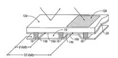
- FIG. 1One interferometric modulator display embodiment comprising an interferometric MEMS display element is illustrated in FIG. 1 .
- the pixelsare in either a bright or dark state.
- the display elementIn the bright (“on” or “open”) state, the display element reflects a large portion of incident visible light to a user.
- the dark (“off” or “closed”) stateWhen in the dark (“off” or “closed”) state, the display element reflects little incident visible light to the user.
- the light reflectance properties of the “on” and “off” statesmay be reversed.
- MEMS pixelscan be configured to reflect predominantly at selected colors, allowing for a color display in addition to black and white.
- FIG. 1is an isometric view depicting two adjacent pixels in a series of pixels of a visual display, wherein each pixel comprises a MEMS interferometric modulator.
- an interferometric modulator displaycomprises a row/column array of these interferometric modulators.
- Each interferometric modulatorincludes a pair of reflective layers positioned at a variable and controllable distance from each other to form a resonant optical cavity with at least one variable dimension.
- one of the reflective layersmay be moved between two positions. In the first position, referred to herein as the relaxed position, the movable reflective layer is positioned at a relatively large distance from a fixed partially reflective layer.
- the movable reflective layerIn the second position, referred to herein as the actuated position, the movable reflective layer is positioned more closely adjacent to the partially reflective layer. Incident light that reflects from the two layers interferes constructively or destructively depending on the position of the movable reflective layer, producing either an overall reflective or non-reflective state for each pixel.
- the depicted portion of the pixel array in FIG. 1includes two adjacent interferometric modulators 12 a and 12 b .
- a movable reflective layer 14 ais illustrated in a relaxed position at a predetermined distance from an optical stack 16 a , which includes a partially reflective layer.
- the movable reflective layer 14 bis illustrated in an actuated position adjacent to the optical stack 16 b.
- optical stack 16typically comprise of several fused layers, which can include an electrode layer, such as indium tin oxide (ITO), a partially reflective layer, such as chromium, and a transparent dielectric.
- ITOindium tin oxide
- the optical stack 16is thus electrically conductive, partially transparent and partially reflective, and may be fabricated, for example, by depositing one or more of the above layers onto a transparent substrate 20 .
- the partially reflective layercan be formed from a variety of materials that are partially reflective such as various metals, semiconductors, and dielectrics. Some examples of suitable materials include oxides, nitrides, and fluorides.
- the partially reflective layercan be formed of one or more layers of materials, and each of the layers can be formed of a single material or a combination of materials.
- the layers of the optical stackare patterned into parallel strips, and may form row electrodes in a display device as described further below.
- the movable reflective layers 14 a , 14 bmay be formed as a series of parallel strips of a deposited metal layer or layers (orthogonal to the row electrodes of 16 a , 16 b ) deposited on top of posts 18 and an intervening sacrificial material deposited between the posts 18 . When the sacrificial material is etched away, the movable reflective layers 14 a , 14 b are separated from the optical stacks 16 a , 16 b by a defined gap 19 .
- a highly conductive and reflective materialsuch as aluminum may be used for the reflective layers 14 , and these strips may form column electrodes in a display device.
- the cavity 19remains between the movable reflective layer 14 a and optical stack 16 a , with the movable reflective layer 14 a in a mechanically relaxed state, as illustrated by the pixel 12 a in FIG. 1 .
- a potential differenceis applied to a selected row and column, the capacitor formed at the intersection of the row and column electrodes at the corresponding pixel becomes charged, and electrostatic forces pull the electrodes together.
- the movable reflective layer 14is deformed and is forced against the optical stack 16 .
- a dielectric layerwithin the optical stack 16 may prevent shorting and control the separation distance between layers 14 and 16 , as illustrated by pixel 12 b on the right in FIG. 1 .
- the behavioris the same regardless of the polarity of the applied potential difference. In this way, row/column actuation that can control the reflective vs. non-reflective pixel states is analogous in many ways to that used in conventional LCD and other display technologies.
- FIGS. 2 through 5illustrate one exemplary process and system for using an array of interferometric modulators in a display application.
- FIG. 2is a system block diagram illustrating one embodiment of an electronic device that may incorporate aspects of the invention.
- the electronic deviceincludes a processor 21 which may be any general purpose single- or multi-chip microprocessor such as an ARM, Pentium®, Pentium II®, Pentium III®, Pentium IV®, Pentium® Pro, an 8051, a MIPS®, a Power PC®, an ALPHA®, or any special purpose microprocessor such as a digital signal processor, microcontroller, or a programmable gate array.
- the processor 21may be configured to execute one or more software modules.
- the processormay be configured to execute one or more software applications, including a web browser, a telephone application, an email program, or any other software application.
- the processor 21is also configured to communicate with an array driver 22 .
- the array driver 22includes a row driver circuit 24 and a column driver circuit 26 that provide signals to a display array or panel 30 .
- the cross section of the array illustrated in FIG. 1is shown by the lines 1 - 1 in FIG. 2 .
- the row/column actuation protocolmay take advantage of a hysteresis property of these devices illustrated in FIG. 3 . It may require, for example, a 10 volt potential difference to cause a movable layer to deform from the relaxed state to the actuated state. However, when the voltage is reduced from that value, the movable layer maintains its state as the voltage drops back below 10 volts.
- the movable layerdoes not relax completely until the voltage drops below 2 volts.
- There is thus a range of voltage, about 3 to 7 V in the example illustrated in FIG. 3where there exists a window of applied voltage within which the device is stable in either the relaxed or actuated state. This is referred to herein as the “hysteresis window” or “stability window.”
- hysteresis windowor “stability window.”
- the row/column actuation protocolcan be designed such that during row strobing, pixels in the strobed row that are to be actuated are exposed to a voltage difference of about 10 volts, and pixels that are to be relaxed are exposed to a voltage difference of close to zero volts. After the strobe, the pixels are exposed to a steady state voltage difference of about 5 volts such that they remain in whatever state the row strobe put them in. After being written, each pixel sees a potential difference within the “stability window” of 3-7 volts in this example. This feature makes the pixel design illustrated in FIG. 1 stable under the same applied voltage conditions in either an actuated or relaxed pre-existing state.
- each pixel of the interferometric modulatoris essentially a capacitor formed by the fixed and moving reflective layers, this stable state can be held at a voltage within the hysteresis window with almost no power dissipation. Essentially no current flows into the pixel if the applied potential is fixed.
- a display framemay be created by asserting the set of column electrodes in accordance with the desired set of actuated pixels in the first row.
- a row pulseis then applied to the row 1 electrode, actuating the pixels corresponding to the asserted column lines.
- the asserted set of column electrodesis then changed to correspond to the desired set of actuated pixels in the second row.
- a pulseis then applied to the row 2 electrode, actuating the appropriate pixels in row 2 in accordance with the asserted column electrodes.
- the row 1 pixelsare unaffected by the row 2 pulse, and remain in the state they were set to during the row 1 pulse. This may be repeated for the entire series of rows in a sequential fashion to produce the frame.
- the framesare refreshed and/or updated with new display data by continually repeating this process at some desired number of frames per second.
- protocols for driving row and column electrodes of pixel arrays to produce display framesare also well known and may be used in conjunction with the present invention.
- FIGS. 4 and 5illustrate one possible actuation protocol for creating a display frame on the 3 ⁇ 3 array of FIG. 2 .
- FIG. 4illustrates a possible set of column and row voltage levels that may be used for pixels exhibiting the hysteresis curves of FIG. 3 .
- actuating a pixelinvolves setting the appropriate column to ⁇ V bias , and the appropriate row to + ⁇ V, which may correspond to ⁇ 5 volts and +5 volts respectively Relaxing the pixel is accomplished by setting the appropriate column to +V bias , and the appropriate row to the same + ⁇ V, producing a zero volt potential difference across the pixel.
- the pixelsare stable in whatever state they were originally in, regardless of whether the column is at +V bias , or ⁇ V bias .
- voltages of opposite polarity than those described abovecan be used, e.g., actuating a pixel can involve setting the appropriate column to +V bias , and the appropriate row to ⁇ V.
- releasing the pixelis accomplished by setting the appropriate column to ⁇ V bias , and the appropriate row to the same ⁇ V, producing a zero volt potential difference across the pixel.
- FIG. 5Bis a timing diagram showing a series of row and column signals applied to the 3 ⁇ 3 array of FIG. 2 which will result in the display arrangement illustrated in FIG. 5A , where actuated pixels are non-reflective.
- the pixelsPrior to writing the frame illustrated in FIG. 5A , the pixels can be in any state, and in this example, all the rows are at 0 volts, and all the columns are at +5 volts. With these applied voltages, all pixels are stable in their existing actuated or relaxed states.
- pixels ( 1 , 1 ), ( 1 , 2 ), ( 2 , 2 ), ( 3 , 2 ) and ( 3 , 3 )are actuated.
- columns 1 and 2are set to ⁇ 5 volts
- column 3is set to +5 volts. This does not change the state of any pixels, because all the pixels remain in the 3-7 volt stability window.
- Row 1is then strobed with a pulse that goes from 0, up to 5 volts, and back to zero. This actuates the (1,1) and (1,2) pixels and relaxes the (1,3) pixel. No other pixels in the array are affected.
- row 2is set to ⁇ 5 volts, and columns 1 and 3 are set to +5 volts.
- the same strobe applied to row 2will then actuate pixel ( 2 , 2 ) and relax pixels ( 2 , 1 ) and ( 2 , 3 ). Again, no other pixels of the array are affected.
- Row 3is similarly set by setting columns 2 and 3 to ⁇ 5 volts, and column 1 to +5 volts.
- the row 3strobe sets the row 3 pixels as shown in FIG. 5A . After writing the frame, the row potentials are zero, and the column potentials can remain at either +5 or ⁇ 5 volts, and the display is then stable in the arrangement of FIG. 5A .
- FIGS. 6A and 6Bare system block diagrams illustrating an embodiment of a display device 40 .
- the display device 40can be, for example, a cellular or mobile telephone.
- the same components of display device 40 or slight variations thereofare also illustrative of various types of display devices such as televisions and portable media players.
- the display device 40includes a housing 41 , a display 30 , an antenna 43 , a speaker 44 , an input device 48 , and a microphone 46 .
- the housing 41is generally formed from any of a variety of manufacturing processes as are well known to those of skill in the art, including injection molding, and vacuum forming.
- the housing 41may be made from any of a variety of materials, including but not limited to plastic, metal, glass, rubber, and ceramic, or a combination thereof.
- the housing 41includes removable portions (not shown) that may be interchanged with other removable portions of different color, or containing different logos, pictures, or symbols.
- the display 30 of exemplary display device 40may be any of a variety of displays, including a bi-stable display, as described herein.
- the display 30includes a flat-panel display, such as plasma, EL, OLED, STN LCD, or TFT LCD as described above, or a non-flat-panel display, such as a CRT or other tube device, as is well known to those of skill in the art.
- the display 30includes an interferometric modulator display, as described herein.
- the components of one embodiment of exemplary display device 40are schematically illustrated in FIG. 6B .
- the illustrated exemplary display device 40includes a housing 41 and can include additional components at least partially enclosed therein.
- the exemplary display device 40includes a network interface 27 that includes an antenna 43 which is coupled to a transceiver 47 .
- the transceiver 47is connected to a processor 21 , which is connected to conditioning hardware 52 .
- the conditioning hardware 52may be configured to condition a signal (e.g. filter a signal).
- the conditioning hardware 52is connected to a speaker 45 and a microphone 46 .
- the processor 21is also connected to an input device 48 and a driver controller 29 .
- the driver controller 29is coupled to a frame buffer 28 , and to an array driver 22 , which in turn is coupled to a display array 30 .
- a power supply 50provides power to all components as required by the particular exemplary display device 40 design.
- the network interface 27includes the antenna 43 and the transceiver 47 so that the exemplary display device 40 can communicate with one ore more devices over a network. In one embodiment the network interface 27 may also have some processing capabilities to relieve requirements of the processor 21 .
- the antenna 43is any antenna known to those of skill in the art for transmitting and receiving signals. In one embodiment, the antenna transmits and receives RF signals according to the IEEE 802.11 standard, including IEEE 802.11(a), (b), or (g). In another embodiment, the antenna transmits and receives RF signals according to the BLUETOOTH standard. In the case of a cellular telephone, the antenna is designed to receive CDMA, GSM, AMPS or other known signals that are used to communicate within a wireless cell phone network.
- the transceiver 47pre-processes the signals received from the antenna 43 so that they may be received by and further manipulated by the processor 21 .
- the transceiver 47also processes signals received from the processor 21 so that they may be transmitted from the exemplary display device 40 via the antenna 43 .
- the transceiver 47can be replaced by a receiver.
- network interface 27can be replaced by an image source, which can store or generate image data to be sent to the processor 21 .
- the image sourcecan be a digital video disc (DVD) or a hard-disc drive that contains image data, or a software module that generates image data.
- Processor 21generally controls the overall operation of the exemplary display device 40 .
- the processor 21receives data, such as compressed image data from the network interface 27 or an image source, and processes the data into raw image data or into a format that is readily processed into raw image data.
- the processor 21then sends the processed data to the driver controller 29 or to frame buffer 28 for storage.
- Raw datatypically refers to the information that identifies the image characteristics at each location within an image. For example, such image characteristics can include color, saturation, and gray-scale level.
- the processor 21includes a microcontroller, CPU, or logic unit to control operation of the exemplary display device 40 .
- Conditioning hardware 52generally includes amplifiers and filters for transmitting signals to the speaker 45 , and for receiving signals from the microphone 46 .
- Conditioning hardware 52may be discrete components within the exemplary display device 40 , or may be incorporated within the processor 21 or other components.
- the driver controller 29takes the raw image data generated by the processor 21 either directly from the processor 21 or from the frame buffer 28 and reformats the raw image data appropriately for high speed transmission to the array driver 22 . Specifically, the driver controller 29 reformats the raw image data into a data flow having a raster-like format, such that it has a time order suitable for scanning across the display array 30 . Then the driver controller 29 sends the formatted information to the array driver 22 .
- a driver controller 29such as a LCD controller, is often associated with the system processor 21 as a stand-alone Integrated Circuit (IC), such controllers may be implemented in many ways. They may be embedded in the processor 21 as hardware, embedded in the processor 21 as software, or fully integrated in hardware with the array driver 22 .
- the array driver 22receives the formatted information from the driver controller 29 and reformats the video data into a parallel set of waveforms that are applied many times per second to the hundreds and sometimes thousands of leads coming from the display's x-y matrix of pixels.
- driver controller 29is a conventional display controller or a bi-stable display controller (e.g., an interferometric modulator controller).
- array driver 22is a conventional driver or a bi-stable display driver (e.g., an interferometric modulator display).
- a driver controller 29is integrated with the array driver 22 .
- display array 30is a typical display array or a bi-stable display array (e.g., a display including an array of interferometric modulators).
- the input device 48allows a user to control the operation of the exemplary display device 40 .
- input device 48includes a keypad, such as a QWERTY keyboard or a telephone keypad, a button, a switch, a touch-sensitive screen, a pressure- or heat-sensitive membrane.
- the microphone 46is an input device for the exemplary display device 40 . When the microphone 46 is used to input data to the device, voice commands may be provided by a user for controlling operations of the exemplary display device 40 .
- Power supply 50can include a variety of energy storage devices as are well known in the art.
- power supply 50is a rechargeable battery, such as a nickel-cadmium battery or a lithium ion battery.
- power supply 50is a renewable energy source, a capacitor, or a solar cell, including a plastic solar cell, and solar-cell paint.
- power supply 50is configured to receive power from a wall outlet.
- control programmabilityresides, as described above, in a driver controller which can be located in several places in the electronic display system. In some cases control programmability resides in the array driver 22 . Those of skill in the art will recognize that the above-described optimization may be implemented in any number of hardware and/or software components and in various configurations.
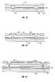
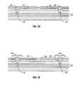
- FIGS. 7A-7Eillustrate five different embodiments of the movable reflective layer 14 and its supporting structures.
- FIG. 7Ais a cross section of the embodiment of FIG. 1 , where a strip of metal material 14 is deposited on orthogonally extending supports 18 .
- FIG. 7Bthe moveable reflective layer 14 is attached to supports at the corners only, on tethers 32 .
- FIG. 7Cthe moveable reflective layer 14 is suspended from a deformable layer 34 , which may comprise a flexible metal.
- the deformable layer 34connects, directly or indirectly, to the substrate 20 around the perimeter of the deformable layer 34 .
- connection postsare herein referred to as support posts.
- the embodiment illustrated in FIG. 7Dhas support post plugs 42 upon which the deformable layer 34 rests.
- the movable reflective layer 14remains suspended over the cavity, as in FIGS. 7A-7C , but the deformable layer 34 does not form the support posts by filling holes between the deformable layer 34 and the optical stack 16 . Rather, the support posts are formed of a planarization material, which is used to form support post plugs 42 .
- the embodiment illustrated in FIG. 7Eis based on the embodiment shown in FIG. 7D , but may also be adapted to work with any of the embodiments illustrated in FIGS. 7A-7C as well as additional embodiments not shown. In the embodiment shown in FIG. 7E , an extra layer of metal or other conductive material has been used to form a bus structure 44 . This allows signal routing along the back of the interferometric modulators, eliminating a number of electrodes that may otherwise have had to be formed on the substrate 20 .
- the interferometric modulatorsfunction as direct-view devices, in which images are viewed from the front side of the transparent substrate 20 , the side opposite to that upon which the modulator is arranged.
- the reflective layer 14optically shields the portions of the interferometric modulator on the side of the reflective layer opposite the substrate 20 , including the deformable layer 34 . This allows the shielded areas to be configured and operated upon without negatively affecting the image quality.
- Such shieldingallows the bus structure 44 in FIG. 7E , which provides the ability to separate the optical properties of the modulator from the electromechanical properties of the modulator, such as addressing and the movements that result from that addressing.
- This separable modulator architectureallows the structural design and materials used for the electromechanical aspects and the optical aspects of the modulator to be selected and to function independently of each other.
- the embodiments shown in FIGS. 7C-7Ehave additional benefits deriving from the decoupling of the optical properties of the reflective layer 14 from its mechanical properties, which are carried out by the deformable layer 34 .
- Thisallows the structural design and materials used for the reflective layer 14 to be optimized with respect to the optical properties, and the structural design and materials used for the deformable layer 34 to be optimized with respect to desired mechanical properties.
- FIGS. 8A and 8Bshow MEMS element 818 which operates as a switch.
- MEMS element 818comprises insulator 808 , which is formed on substrate 820 and supports a portion of mechanical layer 814 .
- Electrode 812is formed on substrate 820 so as to be spaced apart from mechanical layer 814 and is positioned between substrate 820 and mechanical layer 814 near a portion of mechanical layer 814 not supported by insulator 808 .
- MEMS element 818also comprises terminal 810 formed on the substrate so as to be positioned between substrate 820 and mechanical layer 814 near the unsupported end of mechanical layer 814 .
- Operation of the MEMS elementis similar to that of the interferometric modulator MEMS element described above.
- An electrical potential between mechanical layer 814 and electrode 812generates an electromotive force such that the mechanical layer 814 is attracted to electrode 812 .
- the potential, and therefore attractive the electromotive forceis large enough, mechanical layer 814 deflects towards electrode 812 . Accordingly, the end of mechanical layer 814 approaches terminal 810 .
- the deflection of mechanical layer 814is sufficient, mechanical layer 814 contacts terminal 810 and an electrical connection is established between mechanical layer 814 and terminal 810 .
- a signal driven onto mechanical layer 814will be transmitted to terminal 810 .
- a signal driven onto terminal 810will similarly be transmitted to mechanical layer 814 .
- the electric potential between mechanical layer 814 and terminal 810may be reduced until the mechanical restorative force of mechanical layer 814 is greater than the attractive electromotive force between mechanical layer 814 and terminal 810 .
- the mechanical layer 814returns towards a mechanically relaxed position not contacting terminal 810 . The electrical connection is broken and the switch is again open and non-conductive.
- Electrode 812 and terminal 810may comprise one or more metallized semiconductor materials such as, but not limited to, a metal silicide, a metal germanide, and a metal germosilicide (e.g. NiSi, CoSi 2 , MoSi, CoSi, TaSi, TiSi, and Ni(Si x-1 Ge x )) in different crystalline phases and compositions.
- Metallized semiconductor materialscomprise a metal and a semiconductor material such as, but not limited to silicon, germanium, gallium arsenide, Si x-1 Ge x , alloys, and SiC.
- FIG. 8Billustrates MEMS both element 818 of FIG. 8A and transistor 840 on substrate 820 .
- Transistor 840comprises gate electrode 837 , gate oxide 835 , drain electrode 831 , channel region 832 , and source electrode 833 .
- Transistor 840may be configured to directly or indirectly drive MEMS element 818 , or may be configured to directly or indirectly sense a state of MEMS element 818 .
- the material used for electrode 812 and/or terminal 810may be similar to or substantially identical to that used for drain electrode 831 , channel region 832 , and source electrode 833 .
- electrode 812 , drain electrode 831 , channel region 832 , and source electrode 833are formed in substantially the same processing steps.
- FIGS. 9A through 9Dare cross-sections of the MEMS element 818 and transistor 840 at various stages in a manufacturing process.
- semiconductor materialsinclude materials which comprise, for example, at least one of silicon, germanium, and gallium arsenide. These and various other materials with appropriate semiconductor and conductor properties may be used.
- FIG. 9Ashows substrate 920 and semiconductor layer 950 formed on substrate 920 . At this point in the manufacturing process, semiconductor layer 950 may not substantially comprise metal.
- FIG. 9Bshows semiconductor layer 950 after processing such that it is formed into electrode semiconductor 902 , terminal semiconductor 900 , and transistor semiconductor 930 . Transistor gate oxide 935 and transistor gate 937 are then formed over transistor semiconductor 930 , as shown in FIG.
- a metalis subsequently deposited over substrate 920 .
- the metalmay comprise at least one of nickel, molybdenum, cobalt, tantalum, and titanium. Other metals may also be used.
- some of the deposited metalintegrates into the structure of the underlying electrode semiconductor 902 , terminal semiconductor 900 , and transistor semiconductor 930 .
- the resulting materialis advantageous for use both as a conductor, such as electrode 912 and terminal 910 , and as transistor electrodes, such as gate electrode 937 , drain electrode 933 , and source electrode 931 , as shown in FIG. 9C .
- FIG. 9Dshows insulator 908 and mechanical layer 914 fabricated by subsequent processing, so as to complete MEMS element 918 .
- a portion of both a transistor and a MEMS elementmay be substantially simultaneously fabricated. Because metallized semiconductor materials are useful for both conductor applications and transistor electrode and channel applications, such simultaneous fabrication of different portions of a MEMS device is especially advantageous, as these integrated devices can be provided with reduced manufacturing complexity, size, and cost.
- Interferometric modulator 1000Another characteristic of metallized semiconductors is that, in addition to electrical and semiconductor properties, they have optical reflectance properties which allow for advantageous use in optical MEMS devices, such as interferometric modulator 1000 , shown in FIG. 10 . While the following discussion is directed toward interferometric modulator 1000 , the aspects described herein are not limited to this interferometric modulator embodiment, and can be applied to any number of other interferometric modulator embodiments, as well as any other optical MEMS device. Interferometric modulator 1000 of FIG. 10 is similar in structure and function to the interferometric modulators shown in FIGS. 7C-7E .
- Interferometric modulator 1000comprises electrode 1016 formed on substrate 1020 , insulator 1018 formed on electrode 1016 , and reflective layer 1014 supported by deformable mechanical layer 1134 formed above insulator 1018 .
- Interferometric cavity 1010is formed between electrode 1016 and reflective layer 1014 .
- light ⁇is introduced to interferometric cavity 1010 through substrate 1020 , electrode 1016 , and insulator 1018 .
- Light of color and intensity depending on interferometric properties of interferometric cavity 1016is reflected back through insulator 1018 , electrode 1016 , and substrate 1020 . Accordingly, the optical properties and the electrical properties of electrode 1016 both affect the performance of interferometric modulator 1000 .
- Electrode 1016provides an electrical function by serving as a conductor functioning to affect the position of reflective layer 1014 so as to adjust a primary dimension of interferometric cavity 1010 , as described above.
- electrode 1016provides an optical function by serving as a partially reflective layer, which defines a first major boundary of interferometric cavity 1010 , the other major boundary being defined by the reflective layer 1014 .
- these two functions, electrical and opticalare provided by two separate layers.
- transparent ITOor other transparent conductive oxide, e.g.
- ZnOZnO
- Crmay be used as a partially reflective layer, or absorber, defining a first major boundary of the interferometric cavity.
- a metallized semiconductor layeris used to combine and perform the functions of the ITO and Cr layers. Another benefit of using a metallized semiconductor for the electrode/absorber is that the resistivity of metallized semiconductor materials is lower than the resistivity of ITO, as is shown in the following table:
- NiSican be used to form an electrode which is from about 100 ⁇ to about 500 ⁇ .
- a MoSi electrodecan be from about 200 ⁇ to about 1000 ⁇ .
- a CoSi electrodecan be from about 50 ⁇ to about 200 ⁇ , a TaSi electrode can be from about 80 ⁇ to about 350 ⁇ , and a TiSi electrode can be from about 50 ⁇ to about 200 ⁇ .
- the electrical and optical properties of the single metallized semiconductor layercan be tuned by the specific material used for the metallized semiconductor layer and by the thickness of the metallized semiconductor layer, its composition, crystalline phases and dopants. For example, given two metallized semiconductor layers of the same material and different thicknesses, the thicker layer will have less electrical sheet resistance ( ⁇ / ⁇ ) and greater optical reflectance in comparison to the thinner layer.
- processing parameterssuch as, but not limited to, doping concentration, annealing temperature, and annealing time can be used to tune the electrical and optical properties of the metallized semiconductor layer.
- an advantageous aspect of using a metallized semiconductor layer for the electrode/absorberis that semiconductor based electronic devices (e.g. transistors, capacitors, memory devices, and microprocessors) can be manufactured using some of the same processing steps as the interferometric modulator integrated on the same substrate.
- semiconductor based electronic devicese.g. transistors, capacitors, memory devices, and microprocessors
- FIGS. 11A through 11Cshow a manufacturing process that can be used to simultaneously manufacture a MEMS element 1100 and transistor 1140 .
- FIGS. 11A through 11Care cross-sections of the interferometric modulator 1000 and transistor 1140 at various stages in a manufacturing process. The following description is directed towards use of a semiconductor material. For example materials which comprise at least one of silicon, germanium, and gallium arsenide may be used. However, any material with appropriate semiconductor and conductor properties may be used.
- FIG. 11Ashows substrate 1120 and semiconductor layer 1150 formed on substrate 1120 . At this point in the manufacturing process semiconductor layer 1150 may not substantially comprise metal.
- FIG. 11Bshows semiconductor layer 1150 after processing such that semiconductor layer 1150 is formed into electrode semiconductor 1106 and transistor semiconductor 1130 .
- Transistor gate oxide 1135 and transistor gate 1137are subsequently formed over transistor semiconductor 1130 .
- a metalis subsequently deposited over substrate 1120 .
- the metalmay comprise at least one of nickel, molybdenum, cobalt, tantalum, and titanium. Other metals may also be used.
- some of the metalintegrates into the structure of the underlying electrode semiconductor 1106 and transistor semiconductor 1130 .
- the resulting materialis advantageous for use both as a conductor, such as electrode 1116 and as transistor electrodes, such as gate electrode 1137 , drain electrode 1133 , and source electrode 1131 , as is shown in FIG. 11C .
- FIG. 11Calso shows insulator 1118 , reflective layer 1114 , and mechanical layer 1134 fabricated by subsequent processing, so as to complete interferometric modulator 1100 .
- a portion of both a transistor and an interferometric modulatormay be substantially simultaneously fabricated. Because metallized semiconductor materials are useful for optical applications, conductor applications and transistor electrode applications, such simultaneous fabrication of different portions of an optical MEMS device is especially advantageous, as these various applications can be provided with reduced manufacturing complexity, cost and device size.
- the transistor and the MEMS elementmay be may be manufactured or partially manufactured on a thin film transistor (TFT) or semiconductor production line.
- TFTthin film transistor
- TFT'sare transistors in which the drain, source, and channel region of the transistor are formed by depositing a semiconductor over a base substrate.
- the semiconductoris appropriately patterned so as to define the drain, source, and channel regions.
- the base substrateis a non-semiconductor substrate. See, e.g., “Thin Film Transistors—Materials and Processes—Volume 1 Amorphous Silicon Thin Film Transistors,” ed. Yue Kuo, Kluwer Academic Publishers, Boston (2004).
- the base substrate over which the TFT is formedmay be a non-semiconductor such as glass, plastic or metal.
- the semiconductor that is deposited to form the channel region of the TFTmay, for example, comprise silicon (e.g., a-Si, a-SiH) and/or germanium (e.g., a-Ge, a-GeH), and/or gallium arsenide (e.g., a-GaAs), and may also comprise dopants such as phosphorous, arsenic, antimony, and indium.
- silicone.g., a-Si, a-SiH
- germaniume.g., a-Ge, a-GeH
- gallium arsenidee.g., a-GaAs
- dopantssuch as phosphorous, arsenic, antimony, and indium.
- Certain MEMS devicesmay be at least partially processed on a TFT production line simultaneously with certain TFT layers.
- the MEMS device shown in FIG. 8Bcomprising MEMS element 818 and transistor 840 , may be fabricated according to the process described with reference to FIGS. 9A through 9D , where at least some of the fabrication is performed on a TFT production line.
- the processing aspects described with reference to FIGS. 9A through 9Cmay occur on a TFT production line, while the formation of insulator 908 and mechanical layer 914 may be performed on a second production line.
- the TFT production linemay be modified so as to be additionally capable of performing these fabrication steps.
- An interferometric modulatorcomprising ITO as an electrode and Cr as an absorber and an interferometric modulator comprising NiSi as a combined electrode/absorber were each simulated. Certain layers and layer thicknesses and optical performance simulation results are shown in the following table:
- FIGS. 12A and 12Bshow the reflectance of each of the simulated interferometric modulators across wavelengths of visible light. Comparing FIGS. 12A and 12B shows that the interferometric modulator with the metallized semiconductor has better optical performance at least because it has higher reflectance across almost the entire band in the bright state, and has lower reflectance across almost the entire band in the dark state.
Landscapes
- Physics & Mathematics (AREA)
- Engineering & Computer Science (AREA)
- Manufacturing & Machinery (AREA)
- Spectroscopy & Molecular Physics (AREA)
- General Physics & Mathematics (AREA)
- Optics & Photonics (AREA)
- Microelectronics & Electronic Packaging (AREA)
- Mechanical Light Control Or Optical Switches (AREA)
- Electrodes Of Semiconductors (AREA)
Abstract
Description
| RESISTIVITY OF VARIOUS MATERIALS |
| Material | Resistivity (μΩcm) | ||
| ITO | 120-500 | ||
| Nickel silicide | 20-60 | ||
| Molybdenum silicide | ~100 | ||
| Cobalt silicide | 18-25 | ||
| Tantalum silicide | 35-55 | ||
| Titanium silicide | 12-25 | ||
| Material | Resistivity (μΩcm) | ||
| TiSi2 | 13-16 | ||
| ZrSi2 | 35-40 | ||
| HfSi2 | 45-50 | ||
| VSi2 | 50-55 | ||
| 50 | |||
| TaSi2 | 35-45 | ||
| CrSi2 | ~600 | ||
| MoSi2 | ~100 | ||
| WSi2 | ~70 | ||
| FeSi2 | >1000 | ||
| CoSi2 | 18-20 | ||
| NiSi2 | ~50 | ||
| PtSi | 600-800 | ||
| Pd2Si | 400 | ||
| COMPARISON OF DESIGNS WITH Cr/ITO AND NiSi |
| Layer | Cr/ITO design | NiSi design | ||
| Electrode | 500 Å (ITO) | 200 Å (NiSi) | ||
| Absorber | 70 Å (Cr) | No layer needed | ||
| Insulator | 500 Å (Si02)/ | 558 Å (Si02)/ | ||
| 80 Å (Al2O3) | 80 Å (Al2O3) | |||
| Cavity (Bright/Dark) | 1550 Å/0 Å | 1255 Å/0 Å | ||
| Reflective Layer (Al) | 300 Å | 300 | ||
| Mechanical Layer | ||||
| 1000 | 1000 Å | |||
| Optical Performance: | ||||
| 52 | 70 | |||
| 32 | 79 | |||
| u′ v′ | 0.155/0.468 | 0.171/0.470 | ||
Claims (38)
Priority Applications (5)
| Application Number | Priority Date | Filing Date | Title |
|---|---|---|---|
| US11/416,920US7369292B2 (en) | 2006-05-03 | 2006-05-03 | Electrode and interconnect materials for MEMS devices |
| EP07867091AEP2021273A2 (en) | 2006-05-03 | 2007-04-25 | Electrode and interconnect materials for mems devices |
| PCT/US2007/010166WO2008054520A2 (en) | 2006-05-03 | 2007-04-25 | Electrode and interconnect materials for mems interferometric modulators |
| TW096115731ATW200745603A (en) | 2006-05-03 | 2007-05-03 | Electrode and interconnect materials for MEMS devices |
| US12/115,395US7688494B2 (en) | 2006-05-03 | 2008-05-05 | Electrode and interconnect materials for MEMS devices |
Applications Claiming Priority (1)
| Application Number | Priority Date | Filing Date | Title |
|---|---|---|---|
| US11/416,920US7369292B2 (en) | 2006-05-03 | 2006-05-03 | Electrode and interconnect materials for MEMS devices |
Related Child Applications (1)
| Application Number | Title | Priority Date | Filing Date |
|---|---|---|---|
| US12/115,395ContinuationUS7688494B2 (en) | 2006-05-03 | 2008-05-05 | Electrode and interconnect materials for MEMS devices |
Publications (2)
| Publication Number | Publication Date |
|---|---|
| US20070258123A1 US20070258123A1 (en) | 2007-11-08 |
| US7369292B2true US7369292B2 (en) | 2008-05-06 |
Family
ID=38660920
Family Applications (2)
| Application Number | Title | Priority Date | Filing Date |
|---|---|---|---|
| US11/416,920Expired - Fee RelatedUS7369292B2 (en) | 2006-05-03 | 2006-05-03 | Electrode and interconnect materials for MEMS devices |
| US12/115,395Expired - Fee RelatedUS7688494B2 (en) | 2006-05-03 | 2008-05-05 | Electrode and interconnect materials for MEMS devices |
Family Applications After (1)
| Application Number | Title | Priority Date | Filing Date |
|---|---|---|---|
| US12/115,395Expired - Fee RelatedUS7688494B2 (en) | 2006-05-03 | 2008-05-05 | Electrode and interconnect materials for MEMS devices |
Country Status (4)
| Country | Link |
|---|---|
| US (2) | US7369292B2 (en) |
| EP (1) | EP2021273A2 (en) |
| TW (1) | TW200745603A (en) |
| WO (1) | WO2008054520A2 (en) |
Cited By (21)
| Publication number | Priority date | Publication date | Assignee | Title |
|---|---|---|---|---|
| US20070236774A1 (en)* | 2006-04-10 | 2007-10-11 | Evgeni Gousev | Interferometric optical display system with broadband characteristics |
| US20090040590A1 (en)* | 2007-08-07 | 2009-02-12 | Qualcomm Technologies, Inc. | Mems device and interconnects for same |
| US7566664B2 (en) | 2006-08-02 | 2009-07-28 | Qualcomm Mems Technologies, Inc. | Selective etching of MEMS using gaseous halides and reactive co-etchants |
| US20090201565A1 (en)* | 2008-02-12 | 2009-08-13 | Qualcomm Mems Technologies, Inc. | Devices and methods for enhancing brightness of displays using angle conversion layers |
| US20090201571A1 (en)* | 2008-02-12 | 2009-08-13 | Qualcomm Mems Technologies, Inc. | Integrated front light diffuser for reflective displays |
| US7719752B2 (en) | 2007-05-11 | 2010-05-18 | Qualcomm Mems Technologies, Inc. | MEMS structures, methods of fabricating MEMS components on separate substrates and assembly of same |
| US7733552B2 (en) | 2007-03-21 | 2010-06-08 | Qualcomm Mems Technologies, Inc | MEMS cavity-coating layers and methods |
| US20100141557A1 (en)* | 2006-10-06 | 2010-06-10 | Qualcomm Mems Technologies, Inc. | Light guide |
| US20100149624A1 (en)* | 2004-09-27 | 2010-06-17 | Qualcomm Mems Technologies, Inc. | Method and device for compensating for color shift as a function of angle of view |
| WO2011130715A2 (en) | 2010-04-16 | 2011-10-20 | Flex Lighting Ii, Llc | Illumination device comprising a film-based lightguide |
| WO2011130718A2 (en) | 2010-04-16 | 2011-10-20 | Flex Lighting Ii, Llc | Front illumination device comprising a film-based lightguide |
| US8045252B2 (en) | 2004-02-03 | 2011-10-25 | Qualcomm Mems Technologies, Inc. | Spatial light modulator with integrated optical compensation structure |
| US8061882B2 (en) | 2006-10-06 | 2011-11-22 | Qualcomm Mems Technologies, Inc. | Illumination device with built-in light coupler |
| US8368981B2 (en) | 2006-10-10 | 2013-02-05 | Qualcomm Mems Technologies, Inc. | Display device with diffractive optics |
| US8798425B2 (en) | 2007-12-07 | 2014-08-05 | Qualcomm Mems Technologies, Inc. | Decoupled holographic film and diffuser |
| US8902484B2 (en) | 2010-12-15 | 2014-12-02 | Qualcomm Mems Technologies, Inc. | Holographic brightness enhancement film |
| US8928967B2 (en) | 1998-04-08 | 2015-01-06 | Qualcomm Mems Technologies, Inc. | Method and device for modulating light |
| US8971675B2 (en) | 2006-01-13 | 2015-03-03 | Qualcomm Mems Technologies, Inc. | Interconnect structure for MEMS device |
| US9019183B2 (en) | 2006-10-06 | 2015-04-28 | Qualcomm Mems Technologies, Inc. | Optical loss structure integrated in an illumination apparatus |
| US9025235B2 (en) | 2002-12-25 | 2015-05-05 | Qualcomm Mems Technologies, Inc. | Optical interference type of color display having optical diffusion layer between substrate and electrode |
| US9110289B2 (en) | 1998-04-08 | 2015-08-18 | Qualcomm Mems Technologies, Inc. | Device for modulating light with multiple electrodes |
Families Citing this family (15)
| Publication number | Priority date | Publication date | Assignee | Title |
|---|---|---|---|---|
| US20060066586A1 (en)* | 2004-09-27 | 2006-03-30 | Gally Brian J | Touchscreens for displays |
| US20060132383A1 (en)* | 2004-09-27 | 2006-06-22 | Idc, Llc | System and method for illuminating interferometric modulator display |
| KR20100084518A (en)* | 2007-09-17 | 2010-07-26 | 퀄컴 엠이엠스 테크놀로지스, 인크. | Semi-transparent/transflective lighted interferometric modulator devices |
| US8941631B2 (en) | 2007-11-16 | 2015-01-27 | Qualcomm Mems Technologies, Inc. | Simultaneous light collection and illumination on an active display |
| CN101946334B (en)* | 2008-02-12 | 2013-08-21 | 高通Mems科技公司 | Dual layer thin film holographic solar concentrator/collector |
| US8094358B2 (en)* | 2008-03-27 | 2012-01-10 | Qualcomm Mems Technologies, Inc. | Dimming mirror |
| US20090323144A1 (en)* | 2008-06-30 | 2009-12-31 | Qualcomm Mems Technologies, Inc. | Illumination device with holographic light guide |
| US8358266B2 (en) | 2008-09-02 | 2013-01-22 | Qualcomm Mems Technologies, Inc. | Light turning device with prismatic light turning features |
| EP2340567A2 (en)* | 2008-09-18 | 2011-07-06 | QUALCOMM MEMS Technologies, Inc. | Increasing the angular range of light collection in solar collectors/concentrators |
| DE102009009557A1 (en)* | 2009-02-19 | 2010-09-02 | W.C. Heraeus Gmbh | Electrically conductive materials, leads and cables for stimulation electrodes |
| CN102449512A (en) | 2009-05-29 | 2012-05-09 | 高通Mems科技公司 | Illumination devices and methods of fabrication thereof |
| US8470628B2 (en)* | 2011-06-20 | 2013-06-25 | International Business Machines Corporation | Methods to fabricate silicide micromechanical device |
| US9758367B2 (en)* | 2015-12-09 | 2017-09-12 | Analog Devices, Inc. | Metallizing MEMS devices |
| DE102017114085B4 (en) | 2016-06-28 | 2023-05-04 | Analog Devices, Inc. | Selective conductive coating for MEMS sensors |
| US10840320B2 (en)* | 2018-09-28 | 2020-11-17 | Apple Inc. | Ambient light sensing display assemblies |
Citations (399)
| Publication number | Priority date | Publication date | Assignee | Title |
|---|---|---|---|---|
| US2534846A (en) | 1946-06-20 | 1950-12-19 | Emi Ltd | Color filter |
| US3439973A (en) | 1963-06-28 | 1969-04-22 | Siemens Ag | Polarizing reflector for electromagnetic wave radiation in the micron wavelength |
| US3616312A (en) | 1966-04-15 | 1971-10-26 | Ionics | Hydrazine manufacture |
| US3653741A (en) | 1970-02-16 | 1972-04-04 | Alvin M Marks | Electro-optical dipolar material |
| US3656836A (en) | 1968-07-05 | 1972-04-18 | Thomson Csf | Light modulator |
| US3725868A (en) | 1970-10-19 | 1973-04-03 | Burroughs Corp | Small reconfigurable processor for a variety of data processing applications |
| US3813265A (en) | 1970-02-16 | 1974-05-28 | A Marks | Electro-optical dipolar material |
| US3955880A (en) | 1973-07-20 | 1976-05-11 | Organisation Europeenne De Recherches Spatiales | Infrared radiation modulator |
| US4099854A (en) | 1976-10-12 | 1978-07-11 | The Unites States Of America As Represented By The Secretary Of The Navy | Optical notch filter utilizing electric dipole resonance absorption |
| US4196396A (en) | 1976-10-15 | 1980-04-01 | Bell Telephone Laboratories, Incorporated | Interferometer apparatus using electro-optic material with feedback |
| US4228437A (en) | 1979-06-26 | 1980-10-14 | The United States Of America As Represented By The Secretary Of The Navy | Wideband polarization-transforming electromagnetic mirror |
| US4377324A (en) | 1980-08-04 | 1983-03-22 | Honeywell Inc. | Graded index Fabry-Perot optical filter device |
| US4389096A (en) | 1977-12-27 | 1983-06-21 | Matsushita Electric Industrial Co., Ltd. | Image display apparatus of liquid crystal valve projection type |
| US4392711A (en) | 1980-03-28 | 1983-07-12 | Hoechst Aktiengesellschaft | Process and apparatus for rendering visible charge images |
| US4403248A (en) | 1980-03-04 | 1983-09-06 | U.S. Philips Corporation | Display device with deformable reflective medium |
| US4441791A (en) | 1980-09-02 | 1984-04-10 | Texas Instruments Incorporated | Deformable mirror light modulator |
| US4445050A (en) | 1981-12-15 | 1984-04-24 | Marks Alvin M | Device for conversion of light power to electric power |
| US4482213A (en) | 1982-11-23 | 1984-11-13 | Texas Instruments Incorporated | Perimeter seal reinforcement holes for plastic LCDs |
| US4500171A (en) | 1982-06-02 | 1985-02-19 | Texas Instruments Incorporated | Process for plastic LCD fill hole sealing |
| US4519676A (en) | 1982-02-01 | 1985-05-28 | U.S. Philips Corporation | Passive display device |
| US4531126A (en) | 1981-05-18 | 1985-07-23 | Societe D'etude Du Radant | Method and device for analyzing a very high frequency radiation beam of electromagnetic waves |
| US4566935A (en) | 1984-07-31 | 1986-01-28 | Texas Instruments Incorporated | Spatial light modulator and method |
| US4571603A (en) | 1981-11-03 | 1986-02-18 | Texas Instruments Incorporated | Deformable mirror electrostatic printer |
| EP0173808A1 (en) | 1984-07-28 | 1986-03-12 | Deutsche Thomson-Brandt GmbH | Control circuit for liquid-crystal displays |
| US4596992A (en) | 1984-08-31 | 1986-06-24 | Texas Instruments Incorporated | Linear spatial light modulator and printer |
| US4615595A (en) | 1984-10-10 | 1986-10-07 | Texas Instruments Incorporated | Frame addressed spatial light modulator |
| US4617608A (en) | 1984-12-28 | 1986-10-14 | At&T Bell Laboratories | Variable gap device and method of manufacture |
| US4663083A (en) | 1978-05-26 | 1987-05-05 | Marks Alvin M | Electro-optical dipole suspension with reflective-absorptive-transmissive characteristics |
| US4662746A (en) | 1985-10-30 | 1987-05-05 | Texas Instruments Incorporated | Spatial light modulator and method |
| US4681403A (en) | 1981-07-16 | 1987-07-21 | U.S. Philips Corporation | Display device with micromechanical leaf spring switches |
| US4710732A (en) | 1984-07-31 | 1987-12-01 | Texas Instruments Incorporated | Spatial light modulator and method |
| US4748366A (en) | 1986-09-02 | 1988-05-31 | Taylor George W | Novel uses of piezoelectric materials for creating optical effects |
| US4786128A (en) | 1986-12-02 | 1988-11-22 | Quantum Diagnostics, Ltd. | Device for modulating and reflecting electromagnetic radiation employing electro-optic layer having a variable index of refraction |
| US4790635A (en) | 1986-04-25 | 1988-12-13 | The Secretary Of State For Defence In Her Brittanic Majesty's Government Of The United Kingdom Of Great Britain And Northern Ireland | Electro-optical device |
| US4856863A (en) | 1988-06-22 | 1989-08-15 | Texas Instruments Incorporated | Optical fiber interconnection network including spatial light modulator |
| US4859060A (en) | 1985-11-26 | 1989-08-22 | 501 Sharp Kabushiki Kaisha | Variable interferometric device and a process for the production of the same |
| US4900136A (en) | 1987-08-11 | 1990-02-13 | North American Philips Corporation | Method of metallizing silica-containing gel and solid state light modulator incorporating the metallized gel |
| US4900395A (en) | 1989-04-07 | 1990-02-13 | Fsi International, Inc. | HF gas etching of wafers in an acid processor |
| US4937496A (en) | 1987-05-16 | 1990-06-26 | W. C. Heraeus Gmbh | Xenon short arc discharge lamp |
| US4954789A (en) | 1989-09-28 | 1990-09-04 | Texas Instruments Incorporated | Spatial light modulator |
| US4956619A (en) | 1988-02-19 | 1990-09-11 | Texas Instruments Incorporated | Spatial light modulator |
| US4965562A (en) | 1987-05-13 | 1990-10-23 | U.S. Philips Corporation | Electroscopic display device |
| US4982184A (en) | 1989-01-03 | 1991-01-01 | General Electric Company | Electrocrystallochromic display and element |
| US5018256A (en) | 1990-06-29 | 1991-05-28 | Texas Instruments Incorporated | Architecture and process for integrating DMD with control circuit substrates |
| US5022745A (en) | 1989-09-07 | 1991-06-11 | Massachusetts Institute Of Technology | Electrostatically deformable single crystal dielectrically coated mirror |
| US5028939A (en) | 1988-08-23 | 1991-07-02 | Texas Instruments Incorporated | Spatial light modulator system |
| US5037173A (en) | 1989-11-22 | 1991-08-06 | Texas Instruments Incorporated | Optical interconnection network |
| US5044736A (en) | 1990-11-06 | 1991-09-03 | Motorola, Inc. | Configurable optical filter or display |
| US5061049A (en) | 1984-08-31 | 1991-10-29 | Texas Instruments Incorporated | Spatial light modulator and method |
| US5075796A (en) | 1990-05-31 | 1991-12-24 | Eastman Kodak Company | Optical article for multicolor imaging |
| US5078479A (en) | 1990-04-20 | 1992-01-07 | Centre Suisse D'electronique Et De Microtechnique Sa | Light modulation device with matrix addressing |
| US5079544A (en) | 1989-02-27 | 1992-01-07 | Texas Instruments Incorporated | Standard independent digitized video system |
| US5083857A (en) | 1990-06-29 | 1992-01-28 | Texas Instruments Incorporated | Multi-level deformable mirror device |
| US5096279A (en) | 1984-08-31 | 1992-03-17 | Texas Instruments Incorporated | Spatial light modulator and method |
| US5099353A (en) | 1990-06-29 | 1992-03-24 | Texas Instruments Incorporated | Architecture and process for integrating DMD with control circuit substrates |
| US5124834A (en) | 1989-11-16 | 1992-06-23 | General Electric Company | Transferrable, self-supporting pellicle for elastomer light valve displays and method for making the same |
| WO1992010925A1 (en) | 1990-12-11 | 1992-06-25 | Robert Bosch Gmbh | Electrical device, in particular a switching and control device for motor vehicles |
| US5136669A (en) | 1991-03-15 | 1992-08-04 | Sperry Marine Inc. | Variable ratio fiber optic coupler optical signal processing element |
| US5142405A (en) | 1990-06-29 | 1992-08-25 | Texas Instruments Incorporated | Bistable dmd addressing circuit and method |
| US5142414A (en) | 1991-04-22 | 1992-08-25 | Koehler Dale R | Electrically actuatable temporal tristimulus-color device |
| US5153771A (en) | 1990-07-18 | 1992-10-06 | Northrop Corporation | Coherent light modulation and detector |
| US5162787A (en) | 1989-02-27 | 1992-11-10 | Texas Instruments Incorporated | Apparatus and method for digitized video system utilizing a moving display surface |
| US5168406A (en) | 1991-07-31 | 1992-12-01 | Texas Instruments Incorporated | Color deformable mirror device and method for manufacture |
| US5170156A (en) | 1989-02-27 | 1992-12-08 | Texas Instruments Incorporated | Multi-frequency two dimensional display system |
| US5172262A (en) | 1985-10-30 | 1992-12-15 | Texas Instruments Incorporated | Spatial light modulator and method |
| CH681047A5 (en) | 1991-11-25 | 1992-12-31 | Landis & Gyr Betriebs Ag | Measuring parameter, esp. pressure difference, using Fabry-Perot detector - controlling optical length of detector according to output parameter to determine working point on graph |
| US5179274A (en) | 1991-07-12 | 1993-01-12 | Texas Instruments Incorporated | Method for controlling operation of optical systems and devices |
| US5192946A (en) | 1989-02-27 | 1993-03-09 | Texas Instruments Incorporated | Digitized color video display system |
| US5192395A (en) | 1990-10-12 | 1993-03-09 | Texas Instruments Incorporated | Method of making a digital flexure beam accelerometer |
| US5206629A (en) | 1989-02-27 | 1993-04-27 | Texas Instruments Incorporated | Spatial light modulator and memory for digitized video display |
| US5212582A (en) | 1992-03-04 | 1993-05-18 | Texas Instruments Incorporated | Electrostatically controlled beam steering device and method |
| US5214420A (en) | 1989-02-27 | 1993-05-25 | Texas Instruments Incorporated | Spatial light modulator projection system with random polarity light |
| US5214419A (en) | 1989-02-27 | 1993-05-25 | Texas Instruments Incorporated | Planarized true three dimensional display |
| US5216537A (en) | 1990-06-29 | 1993-06-01 | Texas Instruments Incorporated | Architecture and process for integrating DMD with control circuit substrates |
| US5226099A (en) | 1991-04-26 | 1993-07-06 | Texas Instruments Incorporated | Digital micromirror shutter device |
| US5228013A (en) | 1992-01-10 | 1993-07-13 | Bik Russell J | Clock-painting device and method for indicating the time-of-day with a non-traditional, now analog artistic panel of digital electronic visual displays |
| US5231532A (en) | 1992-02-05 | 1993-07-27 | Texas Instruments Incorporated | Switchable resonant filter for optical radiation |
| US5233456A (en) | 1991-12-20 | 1993-08-03 | Texas Instruments Incorporated | Resonant mirror and method of manufacture |
| US5233459A (en) | 1991-03-06 | 1993-08-03 | Massachusetts Institute Of Technology | Electric display device |
| US5233385A (en) | 1991-12-18 | 1993-08-03 | Texas Instruments Incorporated | White light enhanced color field sequential projection |
| US5254980A (en) | 1991-09-06 | 1993-10-19 | Texas Instruments Incorporated | DMD display system controller |
| US5272473A (en) | 1989-02-27 | 1993-12-21 | Texas Instruments Incorporated | Reduced-speckle display system |
| US5278652A (en) | 1991-04-01 | 1994-01-11 | Texas Instruments Incorporated | DMD architecture and timing for use in a pulse width modulated display system |
| US5280277A (en) | 1990-06-29 | 1994-01-18 | Texas Instruments Incorporated | Field updated deformable mirror device |
| US5287096A (en) | 1989-02-27 | 1994-02-15 | Texas Instruments Incorporated | Variable luminosity display system |
| US5293272A (en) | 1992-08-24 | 1994-03-08 | Physical Optics Corporation | High finesse holographic fabry-perot etalon and method of fabricating |
| US5296950A (en) | 1992-01-31 | 1994-03-22 | Texas Instruments Incorporated | Optical signal free-space conversion board |
| US5299041A (en) | 1991-07-11 | 1994-03-29 | France Telecom Etablissement Autonome De Droit Public | Active matrix, high definition, liquid crystal display structure |
| US5311360A (en) | 1992-04-28 | 1994-05-10 | The Board Of Trustees Of The Leland Stanford, Junior University | Method and apparatus for modulating a light beam |
| US5312513A (en) | 1992-04-03 | 1994-05-17 | Texas Instruments Incorporated | Methods of forming multiple phase light modulators |
| US5323002A (en) | 1992-03-25 | 1994-06-21 | Texas Instruments Incorporated | Spatial light modulator based optical calibration system |
| US5325116A (en) | 1992-09-18 | 1994-06-28 | Texas Instruments Incorporated | Device for writing to and reading from optical storage media |
| US5324683A (en) | 1993-06-02 | 1994-06-28 | Motorola, Inc. | Method of forming a semiconductor structure having an air region |
| US5327286A (en) | 1992-08-31 | 1994-07-05 | Texas Instruments Incorporated | Real time optical correlation system |
| US5326430A (en) | 1992-09-24 | 1994-07-05 | International Business Machines Corporation | Cooling microfan arrangements and process |
| US5330617A (en) | 1990-11-16 | 1994-07-19 | France Telecom | Method for etching integrated-circuit layers to a fixed depth and corresponding integrated circuit |
| US5331454A (en) | 1990-11-13 | 1994-07-19 | Texas Instruments Incorporated | Low reset voltage process for DMD |
| US5345328A (en) | 1992-08-12 | 1994-09-06 | Sandia Corporation | Tandem resonator reflectance modulator |
| US5347377A (en) | 1992-06-17 | 1994-09-13 | Eastman Kodak Company | Planar waveguide liquid crystal variable retarder |
| US5355357A (en) | 1990-01-20 | 1994-10-11 | Sony Corporation | Disc player and disc loading device |
| US5358601A (en) | 1991-09-24 | 1994-10-25 | Micron Technology, Inc. | Process for isotropically etching semiconductor devices |
| US5365283A (en) | 1993-07-19 | 1994-11-15 | Texas Instruments Incorporated | Color phase control for projection display using spatial light modulator |
| US5381232A (en) | 1992-05-19 | 1995-01-10 | Akzo Nobel N.V. | Fabry-perot with device mirrors including a dielectric coating outside the resonant cavity |
| US5381253A (en) | 1991-11-14 | 1995-01-10 | Board Of Regents Of University Of Colorado | Chiral smectic liquid crystal optical modulators having variable retardation |
| US5401983A (en) | 1992-04-08 | 1995-03-28 | Georgia Tech Research Corporation | Processes for lift-off of thin film materials or devices for fabricating three dimensional integrated circuits, optical detectors, and micromechanical devices |
| EP0667548A1 (en) | 1994-01-27 | 1995-08-16 | AT&T Corp. | Micromechanical modulator |
| US5444566A (en) | 1994-03-07 | 1995-08-22 | Texas Instruments Incorporated | Optimized electronic operation of digital micromirror devices |
| US5446479A (en) | 1989-02-27 | 1995-08-29 | Texas Instruments Incorporated | Multi-dimensional array video processor system |
| US5448314A (en) | 1994-01-07 | 1995-09-05 | Texas Instruments | Method and apparatus for sequential color imaging |
| US5452024A (en) | 1993-11-01 | 1995-09-19 | Texas Instruments Incorporated | DMD display system |
| US5454906A (en) | 1994-06-21 | 1995-10-03 | Texas Instruments Inc. | Method of providing sacrificial spacer for micro-mechanical devices |
| US5457493A (en) | 1993-09-15 | 1995-10-10 | Texas Instruments Incorporated | Digital micro-mirror based image simulation system |
| US5457566A (en) | 1991-11-22 | 1995-10-10 | Texas Instruments Incorporated | DMD scanner |
| US5459602A (en) | 1993-10-29 | 1995-10-17 | Texas Instruments | Micro-mechanical optical shutter |
| US5461411A (en) | 1993-03-29 | 1995-10-24 | Texas Instruments Incorporated | Process and architecture for digital micromirror printer |
| WO1995030924A1 (en) | 1994-05-05 | 1995-11-16 | Etalon, Inc. | Visible spectrum modulator arrays |
| US5474865A (en) | 1994-11-21 | 1995-12-12 | Sematech, Inc. | Globally planarized binary optical mask using buried absorbers |
| US5489952A (en) | 1993-07-14 | 1996-02-06 | Texas Instruments Incorporated | Method and device for multi-format television |
| EP0695959A1 (en) | 1994-07-29 | 1996-02-07 | AT&T Corp. | Direct view display based on a micromechanical modulator |
| US5497197A (en) | 1993-11-04 | 1996-03-05 | Texas Instruments Incorporated | System and method for packaging data into video processor |
| US5497172A (en) | 1994-06-13 | 1996-03-05 | Texas Instruments Incorporated | Pulse width modulation for spatial light modulator with split reset addressing |
| US5499037A (en) | 1988-09-30 | 1996-03-12 | Sharp Kabushiki Kaisha | Liquid crystal display device for display with gray levels |
| US5499062A (en) | 1994-06-23 | 1996-03-12 | Texas Instruments Incorporated | Multiplexed memory timing with block reset and secondary memory |
| US5500635A (en) | 1990-02-20 | 1996-03-19 | Mott; Jonathan C. | Products incorporating piezoelectric material |
| US5503952A (en) | 1994-03-22 | 1996-04-02 | Shinto Paint Co., Ltd. | Method for manufacture of color filter and liquid crystal display |
| US5506597A (en) | 1989-02-27 | 1996-04-09 | Texas Instruments Incorporated | Apparatus and method for image projection |
| US5517347A (en) | 1993-12-01 | 1996-05-14 | Texas Instruments Incorporated | Direct view deformable mirror device |
| US5526327A (en) | 1994-03-15 | 1996-06-11 | Cordova, Jr.; David J. | Spatial displacement time display |
| US5526051A (en) | 1993-10-27 | 1996-06-11 | Texas Instruments Incorporated | Digital television system |
| US5526172A (en) | 1993-07-27 | 1996-06-11 | Texas Instruments Incorporated | Microminiature, monolithic, variable electrical signal processor and apparatus including same |
| US5526688A (en) | 1990-10-12 | 1996-06-18 | Texas Instruments Incorporated | Digital flexure beam accelerometer and method |
| US5535047A (en) | 1995-04-18 | 1996-07-09 | Texas Instruments Incorporated | Active yoke hidden hinge digital micromirror device |
| US5548301A (en) | 1993-01-11 | 1996-08-20 | Texas Instruments Incorporated | Pixel control circuitry for spatial light modulator |
| US5552925A (en) | 1993-09-07 | 1996-09-03 | John M. Baker | Electro-micro-mechanical shutters on transparent substrates |
| US5552924A (en) | 1994-11-14 | 1996-09-03 | Texas Instruments Incorporated | Micromechanical device having an improved beam |
| US5559358A (en) | 1993-05-25 | 1996-09-24 | Honeywell Inc. | Opto-electro-mechanical device or filter, process for making, and sensors made therefrom |
| US5563398A (en) | 1991-10-31 | 1996-10-08 | Texas Instruments Incorporated | Spatial light modulator scanning system |
| US5567334A (en) | 1995-02-27 | 1996-10-22 | Texas Instruments Incorporated | Method for creating a digital micromirror device using an aluminum hard mask |
| US5579149A (en) | 1993-09-13 | 1996-11-26 | Csem Centre Suisse D'electronique Et De Microtechnique Sa | Miniature network of light obturators |
| US5581272A (en) | 1993-08-25 | 1996-12-03 | Texas Instruments Incorporated | Signal generator for controlling a spatial light modulator |
| US5583688A (en) | 1993-12-21 | 1996-12-10 | Texas Instruments Incorporated | Multi-level digital micromirror device |
| US5597736A (en) | 1992-08-11 | 1997-01-28 | Texas Instruments Incorporated | High-yield spatial light modulator with light blocking layer |
| US5602671A (en) | 1990-11-13 | 1997-02-11 | Texas Instruments Incorporated | Low surface energy passivation layer for micromechanical devices |
| US5610624A (en) | 1994-11-30 | 1997-03-11 | Texas Instruments Incorporated | Spatial light modulator with reduced possibility of an on state defect |
| US5610625A (en) | 1992-05-20 | 1997-03-11 | Texas Instruments Incorporated | Monolithic spatial light modulator and memory package |
| US5610438A (en) | 1995-03-08 | 1997-03-11 | Texas Instruments Incorporated | Micro-mechanical device with non-evaporable getter |
| US5619365A (en) | 1992-06-08 | 1997-04-08 | Texas Instruments Incorporated | Elecronically tunable optical periodic surface filters with an alterable resonant frequency |
| US5619059A (en) | 1994-09-28 | 1997-04-08 | National Research Council Of Canada | Color deformable mirror device having optical thin film interference color coatings |
| US5622814A (en) | 1988-04-20 | 1997-04-22 | Matsushita Electric Industrial Co., Ltd. | Method for fabricating active substrate |
| US5629790A (en) | 1993-10-18 | 1997-05-13 | Neukermans; Armand P. | Micromachined torsional scanner |
| WO1997017628A1 (en) | 1995-11-06 | 1997-05-15 | Etalon, Inc. | Interferometric modulation |
| US5633652A (en) | 1984-02-17 | 1997-05-27 | Canon Kabushiki Kaisha | Method for driving optical modulation device |
| US5636185A (en) | 1995-03-10 | 1997-06-03 | Boit Incorporated | Dynamically changing liquid crystal display timekeeping apparatus |
| US5638084A (en) | 1992-05-22 | 1997-06-10 | Dielectric Systems International, Inc. | Lighting-independent color video display |
| US5638946A (en) | 1996-01-11 | 1997-06-17 | Northeastern University | Micromechanical switch with insulated switch contact |
| US5641391A (en) | 1995-05-15 | 1997-06-24 | Hunter; Ian W. | Three dimensional microfabrication by localized electrodeposition and etching |
| US5646768A (en) | 1994-07-29 | 1997-07-08 | Texas Instruments Incorporated | Support posts for micro-mechanical devices |
| US5647819A (en) | 1993-11-05 | 1997-07-15 | Mitsubishi Jidosha Kogyo Kabushiki Kaisha | Speed change control method for an automatic transmission |
| US5650881A (en) | 1994-11-02 | 1997-07-22 | Texas Instruments Incorporated | Support post architecture for micromechanical devices |
| US5650834A (en) | 1994-07-05 | 1997-07-22 | Mitsubishi Denki Kabushiki Kaisha | Active-matrix device having silicide thin film resistor disposed between an input terminal and a short-circuit ring |
| US5654741A (en) | 1994-05-17 | 1997-08-05 | Texas Instruments Incorporation | Spatial light modulator display pointing device |
| US5659374A (en) | 1992-10-23 | 1997-08-19 | Texas Instruments Incorporated | Method of repairing defective pixels |
| US5665997A (en) | 1994-03-31 | 1997-09-09 | Texas Instruments Incorporated | Grated landing area to eliminate sticking of micro-mechanical devices |
| US5673139A (en) | 1993-07-19 | 1997-09-30 | Medcom, Inc. | Microelectromechanical television scanning device and method for making the same |
| US5674757A (en) | 1994-05-28 | 1997-10-07 | Samsung Electronics Co., Ltd. | Process of fabricating a self-aligned thin-film transistor for a liquid crystal display |
| US5683591A (en) | 1993-05-25 | 1997-11-04 | Robert Bosch Gmbh | Process for producing surface micromechanical structures |
| US5703710A (en) | 1994-09-09 | 1997-12-30 | Deacon Research | Method for manipulating optical energy using poled structure |
| US5706022A (en) | 1994-03-15 | 1998-01-06 | Fujitsu Limited | Optical display device having an optically transparent driver circuit |
| US5710656A (en) | 1996-07-30 | 1998-01-20 | Lucent Technologies Inc. | Micromechanical optical modulator having a reduced-mass composite membrane |
| US5726480A (en) | 1995-01-27 | 1998-03-10 | The Regents Of The University Of California | Etchants for use in micromachining of CMOS Microaccelerometers and microelectromechanical devices and method of making the same |
| US5739945A (en) | 1995-09-29 | 1998-04-14 | Tayebati; Parviz | Electrically tunable optical filter utilizing a deformable multi-layer mirror |
| US5745281A (en) | 1995-12-29 | 1998-04-28 | Hewlett-Packard Company | Electrostatically-driven light modulator and display |
| JPH10148644A (en) | 1996-11-19 | 1998-06-02 | Tdk Corp | Manufacture of minute mechanical element |
| US5771116A (en) | 1996-10-21 | 1998-06-23 | Texas Instruments Incorporated | Multiple bias level reset waveform for enhanced DMD control |
| US5784190A (en) | 1995-04-27 | 1998-07-21 | John M. Baker | Electro-micro-mechanical shutters on transparent substrates |
| US5793504A (en) | 1996-08-07 | 1998-08-11 | Northrop Grumman Corporation | Hybrid angular/spatial holographic multiplexer |
| US5808780A (en) | 1997-06-09 | 1998-09-15 | Texas Instruments Incorporated | Non-contacting micromechanical optical switch |
| JPH10267658A (en) | 1997-03-24 | 1998-10-09 | Nissan Motor Co Ltd | Vibration type angular velocity sensor |
| US5822170A (en) | 1997-10-09 | 1998-10-13 | Honeywell Inc. | Hydrophobic coating for reducing humidity effect in electrostatic actuators |
| US5824608A (en) | 1995-06-27 | 1998-10-20 | Nippondenso Co., Ltd. | Semiconductor physical-quantity sensor and method for manufacturing same |
| US5825528A (en) | 1995-12-26 | 1998-10-20 | Lucent Technologies Inc. | Phase-mismatched fabry-perot cavity micromechanical modulator |
| US5838484A (en) | 1996-08-19 | 1998-11-17 | Lucent Technologies Inc. | Micromechanical optical modulator with linear operating characteristic |
| EP0878824A2 (en) | 1997-05-13 | 1998-11-18 | Surface Technology Systems Limited | Method and apparatus for etching a workpiece |
| US5842088A (en) | 1994-06-17 | 1998-11-24 | Texas Instruments Incorporated | Method of calibrating a spatial light modulator printing system |
| US5867302A (en) | 1997-08-07 | 1999-02-02 | Sandia Corporation | Bistable microelectromechanical actuator |
| US5912758A (en) | 1996-09-11 | 1999-06-15 | Texas Instruments Incorporated | Bipolar reset for spatial light modulators |
| JPH11211999A (en) | 1998-01-28 | 1999-08-06 | Teijin Ltd | Optical modulating element and display device |
| US5943158A (en) | 1998-05-05 | 1999-08-24 | Lucent Technologies Inc. | Micro-mechanical, anti-reflection, switched optical modulator array and fabrication method |
| JPH11243214A (en) | 1998-02-26 | 1999-09-07 | Nippon Telegr & Teleph Corp <Ntt> | Manufacturing method of microstructure |
| WO1999052006A2 (en) | 1998-04-08 | 1999-10-14 | Etalon, Inc. | Interferometric modulation of radiation |
| US5972193A (en) | 1997-10-10 | 1999-10-26 | Industrial Technology Research Institute | Method of manufacturing a planar coil using a transparency substrate |
| US5976902A (en) | 1998-08-03 | 1999-11-02 | Industrial Technology Research Institute | Method of fabricating a fully self-aligned TFT-LCD |
| US6016693A (en) | 1998-02-09 | 2000-01-25 | The Regents Of The University Of California | Microfabrication of cantilevers using sacrificial templates |
| JP2000040831A (en) | 1998-07-22 | 2000-02-08 | Denso Corp | Production method of mechanical sensor of semiconductor |
| US6028690A (en) | 1997-11-26 | 2000-02-22 | Texas Instruments Incorporated | Reduced micromirror mirror gaps for improved contrast ratio |
| US6038056A (en) | 1997-05-08 | 2000-03-14 | Texas Instruments Incorporated | Spatial light modulator having improved contrast ratio |
| US6040937A (en) | 1994-05-05 | 2000-03-21 | Etalon, Inc. | Interferometric modulation |
| US6057903A (en) | 1998-08-18 | 2000-05-02 | International Business Machines Corporation | Liquid crystal display device employing a guard plane between a layer for measuring touch position and common electrode layer |
| US6061075A (en) | 1992-01-23 | 2000-05-09 | Texas Instruments Incorporated | Non-systolic time delay and integration printing |
| KR20000033006A (en) | 1998-11-19 | 2000-06-15 | 하대규 | Method for plasma etching compartment surface of upper side of faraday cage |
| US6100872A (en) | 1993-05-25 | 2000-08-08 | Canon Kabushiki Kaisha | Display control method and apparatus |
| US6099132A (en) | 1994-09-23 | 2000-08-08 | Texas Instruments Incorporated | Manufacture method for micromechanical devices |
| US6115326A (en) | 1998-10-22 | 2000-09-05 | Integrated Medical Systems, Inc. | Ultrasonic micro-machined selectable transducer array |
| US6113239A (en) | 1998-09-04 | 2000-09-05 | Sharp Laboratories Of America, Inc. | Projection display system for reflective light valves |
| US6147790A (en) | 1998-06-02 | 2000-11-14 | Texas Instruments Incorporated | Spring-ring micromechanical device |
| US6160833A (en) | 1998-05-06 | 2000-12-12 | Xerox Corporation | Blue vertical cavity surface emitting laser |
| US6158156A (en) | 1995-10-30 | 2000-12-12 | John Mcgavigan Limited | Display panels |
| US6166422A (en) | 1998-05-13 | 2000-12-26 | Lsi Logic Corporation | Inductor with cobalt/nickel core for integrated circuit structure with high inductance and high Q-factor |
| US6180428B1 (en) | 1997-12-12 | 2001-01-30 | Xerox Corporation | Monolithic scanning light emitting devices using micromachining |
| US6195196B1 (en) | 1998-03-13 | 2001-02-27 | Fuji Photo Film Co., Ltd. | Array-type exposing device and flat type display incorporating light modulator and driving method thereof |
| US6194323B1 (en) | 1998-12-16 | 2001-02-27 | Lucent Technologies Inc. | Deep sub-micron metal etch with in-situ hard mask etch |
| US6201633B1 (en) | 1999-06-07 | 2001-03-13 | Xerox Corporation | Micro-electromechanical based bistable color display sheets |
| US6204080B1 (en) | 1997-10-31 | 2001-03-20 | Daewoo Electronics Co., Ltd. | Method for manufacturing thin film actuated mirror array in an optical projection system |
| US6232936B1 (en) | 1993-12-03 | 2001-05-15 | Texas Instruments Incorporated | DMD Architecture to improve horizontal resolution |
| US6243149B1 (en) | 1994-10-27 | 2001-06-05 | Massachusetts Institute Of Technology | Method of imaging using a liquid crystal display device |
| US6246398B1 (en) | 1997-12-15 | 2001-06-12 | Hyundai Electronics Industries Co., Ltd. | Application specific integrated circuit (ASIC) for driving an external display device |
| US20010003487A1 (en) | 1996-11-05 | 2001-06-14 | Mark W. Miles | Visible spectrum modulator arrays |
| US6249039B1 (en) | 1998-09-10 | 2001-06-19 | Bourns, Inc. | Integrated inductive components and method of fabricating such components |
| US6282010B1 (en) | 1998-05-14 | 2001-08-28 | Texas Instruments Incorporated | Anti-reflective coatings for spatial light modulators |
| US6284560B1 (en) | 1998-12-18 | 2001-09-04 | Eastman Kodak Company | Method for producing co-planar surface structures |
| US6295154B1 (en) | 1998-06-05 | 2001-09-25 | Texas Instruments Incorporated | Optical switching apparatus |
| US20010026951A1 (en) | 1998-07-10 | 2001-10-04 | Paolo Vergani | Method for manufacturing integrated structures including removing a sacrificial region |
| WO2001014248A3 (en) | 1999-08-24 | 2001-10-11 | Knowles Electronics Llc | Assembly process for delicate silicon structures |
| US20010040649A1 (en) | 1999-03-16 | 2001-11-15 | Fujitsu Limited | Manufacturing method of a liquid crystal display |
| US20010040675A1 (en) | 2000-01-28 | 2001-11-15 | True Randall J. | Method for forming a micromechanical device |
| US6323982B1 (en) | 1998-05-22 | 2001-11-27 | Texas Instruments Incorporated | Yield superstructure for digital micromirror device |
| US6327071B1 (en) | 1998-10-16 | 2001-12-04 | Fuji Photo Film Co., Ltd. | Drive methods of array-type light modulation element and flat-panel display |
| US6329297B1 (en) | 2000-04-21 | 2001-12-11 | Applied Materials, Inc. | Dilute remote plasma clean |
| US6335831B2 (en) | 1998-12-18 | 2002-01-01 | Eastman Kodak Company | Multilevel mechanical grating device |
| US20020015215A1 (en) | 1994-05-05 | 2002-02-07 | Iridigm Display Corporation, A Delaware Corporation | Interferometric modulation of radiation |
| US20020021485A1 (en) | 2000-07-13 | 2002-02-21 | Nissim Pilossof | Blazed micro-mechanical light modulator and array thereof |
| US6351329B1 (en) | 1999-10-08 | 2002-02-26 | Lucent Technologies Inc. | Optical attenuator |
| JP2002062493A (en) | 2000-08-21 | 2002-02-28 | Canon Inc | Display element using coherent modulation element |
| US20020024711A1 (en) | 1994-05-05 | 2002-02-28 | Iridigm Display Corporation, A Delaware Corporation | Interferometric modulation of radiation |
| US6356254B1 (en) | 1998-09-25 | 2002-03-12 | Fuji Photo Film Co., Ltd. | Array-type light modulating device and method of operating flat display unit |
| WO2002024570A1 (en) | 2000-09-25 | 2002-03-28 | Bookham Technology Plc | Micro electro-mechanical systems |
| US20020036304A1 (en) | 1998-11-25 | 2002-03-28 | Raytheon Company, A Delaware Corporation | Method and apparatus for switching high frequency signals |
| US6376787B1 (en) | 2000-08-24 | 2002-04-23 | Texas Instruments Incorporated | Microelectromechanical switch with fixed metal electrode/dielectric interface with a protective cap layer |
| US20020055253A1 (en) | 2000-11-09 | 2002-05-09 | Joachim Rudhard | Method for producing a micromechanical structure and a micromechanical structure |
| US20020054424A1 (en) | 1994-05-05 | 2002-05-09 | Etalon, Inc. | Photonic mems and structures |
| US6392781B1 (en) | 1999-09-15 | 2002-05-21 | Electronics And Telecommunications Research Institute | High speed semiconductor optical modulator and fabricating method thereof |
| US6392233B1 (en) | 2000-08-10 | 2002-05-21 | Sarnoff Corporation | Optomechanical radiant energy detector |
| US20020071169A1 (en) | 2000-02-01 | 2002-06-13 | Bowers John Edward | Micro-electro-mechanical-system (MEMS) mirror device |
| US6407851B1 (en) | 2000-08-01 | 2002-06-18 | Mohammed N. Islam | Micromechanical optical switch |
| US20020086455A1 (en) | 2000-12-21 | 2002-07-04 | Martin Franosch | Method for the manufacture of micro-mechanical components |
| US6452465B1 (en) | 2000-06-27 | 2002-09-17 | M-Squared Filters, Llc | High quality-factor tunable resonator |
| JP2002270575A (en) | 2001-03-13 | 2002-09-20 | Seiko Epson Corp | Etching method, semiconductor device and etching apparatus manufactured by this method |
| US6456420B1 (en) | 2000-07-27 | 2002-09-24 | Mcnc | Microelectromechanical elevating structures |
| US20020135857A1 (en) | 2001-03-26 | 2002-09-26 | Fitzpatrick Glen Arthur | High frequency deformable mirror device |
| US20020137072A1 (en) | 1996-07-29 | 2002-09-26 | Nanosphere, Inc. | Nanoparticles having oligonucleotides attached thereto and uses therefor |
| US6465355B1 (en) | 2001-04-27 | 2002-10-15 | Hewlett-Packard Company | Method of fabricating suspended microstructures |
| US6466358B2 (en) | 1999-12-30 | 2002-10-15 | Texas Instruments Incorporated | Analog pulse width modulation cell for digital micromechanical device |
| US6466354B1 (en) | 2000-09-19 | 2002-10-15 | Silicon Light Machines | Method and apparatus for interferometric modulation of light |
| US20020149828A1 (en) | 1994-05-05 | 2002-10-17 | Miles Mark W. | Controlling micro-electro-mechanical cavities |
| US6473274B1 (en) | 2000-06-28 | 2002-10-29 | Texas Instruments Incorporated | Symmetrical microactuator structure for use in mass data storage devices, or the like |
| US6480177B2 (en) | 1997-06-04 | 2002-11-12 | Texas Instruments Incorporated | Blocked stepped address voltage for micromechanical devices |
| US20020168136A1 (en) | 2001-05-08 | 2002-11-14 | Axsun Technologies, Inc. | Suspended high reflectivity coating on release structure and fabrication process therefor |
| EP1258860A1 (en) | 2001-05-09 | 2002-11-20 | Eastman Kodak Company | Drive circuit for cholesteric liquid crystal displays |
| JP2002355800A (en) | 2001-05-30 | 2002-12-10 | Samsung Electronics Co Ltd | Method for producing anti-adhesion microstructure |
| US6496122B2 (en) | 1998-06-26 | 2002-12-17 | Sharp Laboratories Of America, Inc. | Image display and remote control system capable of displaying two distinct images |
| JP2003001598A (en) | 2001-06-21 | 2003-01-08 | Sony Corp | ETCHING METHOD OF Si FILM |
| US20030006468A1 (en) | 2001-06-27 | 2003-01-09 | Qing Ma | Sacrificial layer technique to make gaps in mems applications |
| WO2003007049A1 (en) | 1999-10-05 | 2003-01-23 | Iridigm Display Corporation | Photonic mems and structures |
| US6513911B1 (en) | 1999-06-04 | 2003-02-04 | Canon Kabushiki Kaisha | Micro-electromechanical device, liquid discharge head, and method of manufacture therefor |
| US6522801B1 (en) | 2000-10-10 | 2003-02-18 | Agere Systems Inc. | Micro-electro-optical mechanical device having an implanted dopant included therein and a method of manufacture therefor |
| US6531945B1 (en) | 2000-03-10 | 2003-03-11 | Micron Technology, Inc. | Integrated circuit inductor with a magnetic core |
| US20030054588A1 (en) | 2000-12-07 | 2003-03-20 | Reflectivity, Inc., A California Corporation | Methods for depositing, releasing and packaging micro-electromechanical devices on wafer substrates |
| US6537427B1 (en) | 1999-02-04 | 2003-03-25 | Micron Technology, Inc. | Deposition of smooth aluminum films |
| US20030062186A1 (en) | 2001-09-21 | 2003-04-03 | Eastman Kodak Company | Sealing structure for highly moisture-sensitive electronic device element and method for fabrication |
| US6545335B1 (en) | 1999-12-27 | 2003-04-08 | Xerox Corporation | Structure and method for electrical isolation of optoelectronic integrated circuits |
| US6548908B2 (en) | 1999-12-27 | 2003-04-15 | Xerox Corporation | Structure and method for planar lateral oxidation in passive devices |
| US6549338B1 (en) | 1999-11-12 | 2003-04-15 | Texas Instruments Incorporated | Bandpass filter to reduce thermal impact of dichroic light shift |
| US6552840B2 (en) | 1999-12-03 | 2003-04-22 | Texas Instruments Incorporated | Electrostatic efficiency of micromechanical devices |
| US20030090350A1 (en) | 2001-11-13 | 2003-05-15 | The Board Of Trustees Of The University Of Illinos | Electromagnetic energy controlled low actuation voltage microelectromechanical switch |
| US6574033B1 (en) | 2002-02-27 | 2003-06-03 | Iridigm Display Corporation | Microelectromechanical systems device and method for fabricating same |
| US6577785B1 (en) | 2001-08-09 | 2003-06-10 | Sandia Corporation | Compound semiconductor optical waveguide switch |
| US20030112096A1 (en) | 2001-09-13 | 2003-06-19 | Potter Michael D. | Resonator and a method of making thereof |
| WO2003052506A1 (en) | 2001-12-18 | 2003-06-26 | Nokia Corporation | Electrically tunable interferometric filter |
| US6589625B1 (en) | 2001-08-01 | 2003-07-08 | Iridigm Display Corporation | Hermetic seal and method to create the same |
| US20030138213A1 (en) | 2002-01-22 | 2003-07-24 | Lucent Technologies | Optical systems comprising curved MEMs mirrors and methods for making same |
| US6600201B2 (en) | 2001-08-03 | 2003-07-29 | Hewlett-Packard Development Company, L.P. | Systems with high density packing of micromachines |
| US6606175B1 (en) | 1999-03-16 | 2003-08-12 | Sharp Laboratories Of America, Inc. | Multi-segment light-emitting diode |
| US20030152872A1 (en) | 2002-02-12 | 2003-08-14 | Miles Mark W. | Method for fabricating a structure for a microelectromechanical systems (MEMS) device |
| US6608268B1 (en) | 2002-02-05 | 2003-08-19 | Memtronics, A Division Of Cogent Solutions, Inc. | Proximity micro-electro-mechanical system |
| US6610440B1 (en) | 1998-03-10 | 2003-08-26 | Bipolar Technologies, Inc | Microscopic batteries for MEMS systems |
| US6625047B2 (en) | 2000-12-31 | 2003-09-23 | Texas Instruments Incorporated | Micromechanical memory element |
| US6630786B2 (en) | 2001-03-30 | 2003-10-07 | Candescent Technologies Corporation | Light-emitting device having light-reflective layer formed with, or/and adjacent to, material that enhances device performance |
| US6632698B2 (en) | 2001-08-07 | 2003-10-14 | Hewlett-Packard Development Company, L.P. | Microelectromechanical device having a stiffened support beam, and methods of forming stiffened support beams in MEMS |
| US6635919B1 (en) | 2000-08-17 | 2003-10-21 | Texas Instruments Incorporated | High Q-large tuning range micro-electro mechanical system (MEMS) varactor for broadband applications |
| US20030201784A1 (en) | 2001-09-13 | 2003-10-30 | Potter Michael D. | Biohazard sensing system and methods thereof |
| US20030202266A1 (en) | 2002-04-30 | 2003-10-30 | Ring James W. | Micro-mirror device with light angle amplification |
| US20030202265A1 (en) | 2002-04-30 | 2003-10-30 | Reboa Paul F. | Micro-mirror device including dielectrophoretic liquid |
| US20030202264A1 (en) | 2002-04-30 | 2003-10-30 | Weber Timothy L. | Micro-mirror device |
| US6642913B1 (en) | 1999-01-20 | 2003-11-04 | Fuji Photo Film Co., Ltd. | Light modulation element, exposure unit, and flat-panel display unit |
| US6643069B2 (en) | 2000-08-31 | 2003-11-04 | Texas Instruments Incorporated | SLM-base color projection display having multiple SLM's and multiple projection lenses |
| US6657832B2 (en) | 2001-04-26 | 2003-12-02 | Texas Instruments Incorporated | Mechanically assisted restoring force support for micromachined membranes |
| US20030231373A1 (en) | 2002-06-12 | 2003-12-18 | Eastman Kodak Compay | High-contrast display system with scanned conformal grating device |
| US6666561B1 (en) | 2002-10-28 | 2003-12-23 | Hewlett-Packard Development Company, L.P. | Continuously variable analog micro-mirror device |
| US6674033B1 (en) | 2002-08-21 | 2004-01-06 | Ming-Shan Wang | Press button type safety switch |
| US20040010115A1 (en) | 2002-07-11 | 2004-01-15 | Sotzing Gregory Allen | Polymers comprising thieno [3,4-b]thiophene and methods of making and using the same |
| WO2004006003A1 (en) | 2002-07-02 | 2004-01-15 | Iridigm Display Corporation | A device having a light-absorbing mask a method for fabricating same |
| DE10228946A1 (en) | 2002-06-28 | 2004-01-22 | Universität Bremen | Optical modulator, used in projection displays, comprises a base layer arranged on a substrate, a membrane layer, and devices for applying an electrical voltage between the membrane layer and the substrate |
| US20040027701A1 (en) | 2001-07-12 | 2004-02-12 | Hiroichi Ishikawa | Optical multilayer structure and its production method, optical switching device, and image display |
| US20040028849A1 (en) | 2002-04-18 | 2004-02-12 | Stark Brian H. | Low temperature method for forming a microcavity on a substrate and article having same |
| US20040035821A1 (en) | 1999-10-26 | 2004-02-26 | Doan Jonathan C. | Methods for forming and releasing microelectromechanical structures |
| US20040051929A1 (en) | 1994-05-05 | 2004-03-18 | Sampsell Jeffrey Brian | Separable modulator |
| US20040053434A1 (en) | 2001-09-13 | 2004-03-18 | Silicon Light Machines | Microelectronic mechanical system and methods |
| US20040058531A1 (en) | 2002-08-08 | 2004-03-25 | United Microelectronics Corp. | Method for preventing metal extrusion in a semiconductor structure. |
| US20040058532A1 (en) | 2002-09-20 | 2004-03-25 | Miles Mark W. | Controlling electromechanical behavior of structures within a microelectromechanical systems device |
| US20040061543A1 (en) | 2002-09-26 | 2004-04-01 | Yun-Woo Nam | Flexible MEMS transducer and manufacturing method thereof, and flexible MEMS wireless microphone |
| US20040063322A1 (en) | 2000-11-02 | 2004-04-01 | Eui-Hyeok Yang | Wafer-level transfer of membranes with gas-phase etching and wet etching methods |
| JP2004102022A (en) | 2002-09-11 | 2004-04-02 | Ricoh Co Ltd | Image forming device |
| JP2004106074A (en) | 2002-09-13 | 2004-04-08 | Sony Corp | Production method for hollow structure and production method for mems element |
| US6720267B1 (en) | 2003-03-19 | 2004-04-13 | United Microelectronics Corp. | Method for forming a cantilever beam model micro-electromechanical system |
| US20040080807A1 (en) | 2002-10-24 | 2004-04-29 | Zhizhang Chen | Mems-actuated color light modulator and methods |
| US20040087086A1 (en) | 2002-10-23 | 2004-05-06 | Wook-Hyoung Lee | Non-volatile memory device to protect floating gate from charge loss and method for fabricating the same |
| US6736987B1 (en) | 2000-07-12 | 2004-05-18 | Techbank Corporation | Silicon etching apparatus using XeF2 |
| US6741503B1 (en) | 2002-12-04 | 2004-05-25 | Texas Instruments Incorporated | SLM display data address mapping for four bank frame buffer |
| US6741384B1 (en) | 2003-04-30 | 2004-05-25 | Hewlett-Packard Development Company, L.P. | Control of MEMS and light modulator arrays |
| US20040100677A1 (en) | 2000-12-07 | 2004-05-27 | Reflectivity, Inc., A California Corporation | Spatial light modulators with light blocking/absorbing areas |
| US6743570B2 (en) | 2001-05-25 | 2004-06-01 | Cornell Research Foundation, Inc. | Method of using heat-depolymerizable polycarbonate sacrificial layer to create nano-fluidic devices |
| US6747800B1 (en) | 2002-12-27 | 2004-06-08 | Prime View International Co., Ltd. | Optical interference type panel and the manufacturing method thereof |
| US6756317B2 (en) | 2001-04-23 | 2004-06-29 | Memx, Inc. | Method for making a microstructure by surface micromachining |
| US20040125536A1 (en) | 2002-12-18 | 2004-07-01 | Susanne Arney | Charge dissipation in electrostatically driven devices |
| US20040124073A1 (en) | 2002-05-07 | 2004-07-01 | Pillans Brandon W. | Micro-electro-mechanical switch, and methods of making and using it |
| US20040125281A1 (en) | 2002-12-25 | 2004-07-01 | Wen-Jian Lin | Optical interference type of color display |
| US20040125282A1 (en) | 2002-12-27 | 2004-07-01 | Wen-Jian Lin | Optical interference color display and optical interference modulator |
| US20040136076A1 (en) | 1995-09-29 | 2004-07-15 | Parviz Tayebati | Electrically tunable fabry-perot structure utilizing a deformable multi-layer mirror and method of making the same |
| US6768097B1 (en) | 2001-02-05 | 2004-07-27 | Centre National De La Recherche Scientifique | Optoelectronic device with wavelength filtering by cavity coupling |
| US20040147198A1 (en) | 2003-01-29 | 2004-07-29 | Prime View International Co., Ltd. | Optical-interference type display panel and method for making the same |
| US20040145049A1 (en) | 2003-01-29 | 2004-07-29 | Mckinnell James C. | Micro-fabricated device with thermoelectric device and method of making |
| US20040147056A1 (en) | 2003-01-29 | 2004-07-29 | Mckinnell James C. | Micro-fabricated device and method of making |
| JP2004212656A (en) | 2002-12-27 | 2004-07-29 | Fuji Photo Film Co Ltd | Optical modulator array and plane display |
| US20040148009A1 (en) | 2001-10-12 | 2004-07-29 | Jon Buzzard | Locking handle deployment mechanism for medical device and method |
| US20040145811A1 (en) | 2003-01-29 | 2004-07-29 | Prime View International Co., Ltd. | Optical-interference type reflective panel and method for making the same |
| US20040150869A1 (en) | 2002-02-19 | 2004-08-05 | Hiroto Kasai | Mems device and methods for manufacturing thereof, light modulation device, glv device and methods for manufacturing thereof, and laser display |
| US6775174B2 (en) | 2000-12-28 | 2004-08-10 | Texas Instruments Incorporated | Memory architecture for micromirror cell |
| US6778306B2 (en) | 2001-04-23 | 2004-08-17 | Memx, Inc. | Surface micromachined optical system with reinforced mirror microstructure |
| US6778155B2 (en) | 2000-07-31 | 2004-08-17 | Texas Instruments Incorporated | Display operation with inserted block clears |
| US20040160143A1 (en) | 2003-02-14 | 2004-08-19 | Shreeve Robert W. | Micro-mirror device with increased mirror tilt |
| US20040175577A1 (en) | 2003-03-05 | 2004-09-09 | Prime View International Co., Ltd. | Structure of a light-incidence electrode of an optical interference display plate |
| US20040179445A1 (en) | 2003-03-13 | 2004-09-16 | Park Yong Cheol | Write-once recording medium and defective area management method and apparatus for write-once recording medium |
| US20040179281A1 (en) | 2003-03-12 | 2004-09-16 | Reboa Paul F. | Micro-mirror device including dielectrophoretic liquid |
| US20040191937A1 (en) | 2003-03-28 | 2004-09-30 | Patel Satyadev R. | Barrier layers for microelectromechanical systems |
| US20040209195A1 (en) | 2003-04-21 | 2004-10-21 | Wen-Jian Lin | Method for fabricating an interference display unit |
| US20040207897A1 (en) | 2003-04-21 | 2004-10-21 | Wen-Jian Lin | Method for fabricating an interference display unit |
| US20040209192A1 (en) | 2003-04-21 | 2004-10-21 | Prime View International Co., Ltd. | Method for fabricating an interference display unit |
| US20040212026A1 (en) | 2002-05-07 | 2004-10-28 | Hewlett-Packard Company | MEMS device having time-varying control |
| US6811267B1 (en) | 2003-06-09 | 2004-11-02 | Hewlett-Packard Development Company, L.P. | Display system with nonvisible data projection |
| US6812482B2 (en) | 1999-04-21 | 2004-11-02 | Sandia Corporation | Method to fabricate layered material compositions |
| US20040218251A1 (en) | 2003-04-30 | 2004-11-04 | Arthur Piehl | Optical interference pixel display with charge control |
| US20040218334A1 (en) | 2003-04-30 | 2004-11-04 | Martin Eric T | Selective update of micro-electromechanical device |
| US20040217919A1 (en) | 2003-04-30 | 2004-11-04 | Arthur Piehl | Self-packaged optical interference display device having anti-stiction bumps, integral micro-lens, and reflection-absorbing layers |
| US20040218341A1 (en) | 2003-04-30 | 2004-11-04 | Martin Eric T. | Charge control of micro-electromechanical device |
| US20040217378A1 (en) | 2003-04-30 | 2004-11-04 | Martin Eric T. | Charge control circuit for a micro-electromechanical device |
| US6819469B1 (en) | 2003-05-05 | 2004-11-16 | Igor M. Koba | High-resolution spatial light modulator for 3-dimensional holographic display |
| US20040227493A1 (en) | 2003-04-30 | 2004-11-18 | Van Brocklin Andrew L. | System and a method of driving a parallel-plate variable micro-electromechanical capacitor |
| US6822628B2 (en) | 2001-06-28 | 2004-11-23 | Candescent Intellectual Property Services, Inc. | Methods and systems for compensating row-to-row brightness variations of a field emission display |
| US20040240138A1 (en) | 2003-05-14 | 2004-12-02 | Eric Martin | Charge control circuit |
| US20040240027A1 (en) | 2003-05-26 | 2004-12-02 | Prime View International Co., Ltd. | Structure of a structure release and a method for manufacturing the same |
| US20040245588A1 (en) | 2003-06-03 | 2004-12-09 | Nikkel Eric L. | MEMS device and method of forming MEMS device |
| US20040263944A1 (en) | 2003-06-24 | 2004-12-30 | Miles Mark W. | Thin film precursor stack for MEMS manufacturing |
| US20050003667A1 (en) | 2003-05-26 | 2005-01-06 | Prime View International Co., Ltd. | Method for fabricating optical interference display cell |
| US20050020089A1 (en) | 2002-03-22 | 2005-01-27 | Hongqin Shi | Etching method used in fabrications of microstructures |
| US6853129B1 (en) | 2000-07-28 | 2005-02-08 | Candescent Technologies Corporation | Protected substrate structure for a field emission display device |
| US6855610B2 (en) | 2002-09-18 | 2005-02-15 | Promos Technologies, Inc. | Method of forming self-aligned contact structure with locally etched gate conductive layer |
| US20050038950A1 (en) | 2003-08-13 | 2005-02-17 | Adelmann Todd C. | Storage device having a probe and a storage cell with moveable parts |
| US20050035699A1 (en) | 2003-08-15 | 2005-02-17 | Hsiung-Kuang Tsai | Optical interference display panel |
| US20050036192A1 (en) | 2003-08-15 | 2005-02-17 | Wen-Jian Lin | Optical interference display panel |
| US20050036095A1 (en) | 2003-08-15 | 2005-02-17 | Jia-Jiun Yeh | Color-changeable pixels of an optical interference display panel |
| US6859218B1 (en) | 2000-11-07 | 2005-02-22 | Hewlett-Packard Development Company, L.P. | Electronic display devices and methods |
| JP2005051007A (en) | 2003-07-28 | 2005-02-24 | Tokyo Electron Ltd | Manufacturing method of semiconductor chip |
| US20050042117A1 (en) | 2003-08-18 | 2005-02-24 | Wen-Jian Lin | Optical interference display panel and manufacturing method thereof |
| US6862029B1 (en) | 1999-07-27 | 2005-03-01 | Hewlett-Packard Development Company, L.P. | Color display system |
| US6862022B2 (en) | 2001-07-20 | 2005-03-01 | Hewlett-Packard Development Company, L.P. | Method and system for automatically selecting a vertical refresh rate for a video display monitor |
| US6861277B1 (en) | 2003-10-02 | 2005-03-01 | Hewlett-Packard Development Company, L.P. | Method of forming MEMS device |
| US20050046948A1 (en) | 2003-08-26 | 2005-03-03 | Wen-Jian Lin | Interference display cell and fabrication method thereof |
| US20050046922A1 (en) | 2003-09-03 | 2005-03-03 | Wen-Jian Lin | Interferometric modulation pixels and manufacturing method thereof |
| US6868208B2 (en)* | 2000-08-30 | 2005-03-15 | France Telecom | Apodization method for a bragg grating |
| US20050057442A1 (en) | 2003-08-28 | 2005-03-17 | Olan Way | Adjacent display of sequential sub-images |
| US6870581B2 (en) | 2001-10-30 | 2005-03-22 | Sharp Laboratories Of America, Inc. | Single panel color video projection display using reflective banded color falling-raster illumination |
| US20050068606A1 (en) | 2003-09-26 | 2005-03-31 | Prime View International Co., Ltd. | Color changeable pixel |
| US20050069209A1 (en) | 2003-09-26 | 2005-03-31 | Niranjan Damera-Venkata | Generating and displaying spatially offset sub-frames |
| US20050068583A1 (en) | 2003-09-30 | 2005-03-31 | Gutkowski Lawrence J. | Organizing a digital image |
| US20050078348A1 (en) | 2003-09-30 | 2005-04-14 | Wen-Jian Lin | Structure of a micro electro mechanical system and the manufacturing method thereof |
| US6882458B2 (en) | 2003-04-21 | 2005-04-19 | Prime View International Co., Ltd. | Structure of an optical interference display cell |
| US6882461B1 (en) | 2004-02-18 | 2005-04-19 | Prime View International Co., Ltd | Micro electro mechanical system display cell and method for fabricating thereof |
| US20050195467A1 (en) | 2004-03-03 | 2005-09-08 | Manish Kothari | Altering temporal response of microelectromechanical elements |
| US20050195462A1 (en) | 2004-03-05 | 2005-09-08 | Prime View International Co., Ltd. | Interference display plate and manufacturing method thereof |
| US20050202649A1 (en) | 2004-03-10 | 2005-09-15 | Po-Chung Hung | Optical interference reflective element and repairing and manufacturing methods thereof |
| US6952304B2 (en) | 2001-01-30 | 2005-10-04 | Matsushita Electric Industrial Co., Ltd. | Variable mirror and information apparatus comprising variable mirror |
| US6952303B2 (en) | 2003-08-29 | 2005-10-04 | Prime View International Co., Ltd | Interferometric modulation pixels and manufacturing method thereof |
| US6958847B2 (en) | 2004-01-20 | 2005-10-25 | Prime View International Co., Ltd. | Structure of an optical interference display unit |
| US20060056001A1 (en)* | 2004-09-02 | 2006-03-16 | Ayumu Taguchi | Aggregate of electronic device chips, electronic device chip, aggregate of diffraction grating light modulators, and diffraction grating light modulator |
| US20060067650A1 (en)* | 2004-09-27 | 2006-03-30 | Clarence Chui | Method of making a reflective display device using thin film transistor production techniques |
| US20060066932A1 (en)* | 2004-09-27 | 2006-03-30 | Clarence Chui | Method of selective etching using etch stop layer |
| WO2006036437A1 (en) | 2004-09-27 | 2006-04-06 | Idc, Llc | Device and method for modifying actuation voltage thresholds of a deformable membrane in an interferometric modulator |
| WO2006036542A1 (en) | 2004-09-27 | 2006-04-06 | Idc, Llc | Interferometric optical modulator using filler material and method |
| WO2006036385A1 (en) | 2004-09-27 | 2006-04-06 | Idc, Llc | Mems device fabricated on a pre-patterned substrate |
Family Cites Families (90)
| Publication number | Priority date | Publication date | Assignee | Title |
|---|---|---|---|---|
| US4863245A (en) | 1984-02-28 | 1989-09-05 | Exxon Research And Engineering Company | Superlattice electrooptic devices |
| US5218472A (en)* | 1989-03-22 | 1993-06-08 | Alcan International Limited | Optical interference structures incorporating porous films |
| CH680534A5 (en) | 1991-09-16 | 1992-09-15 | Landis & Gyr Betriebs Ag | Fabry=perot sensor for optical parameter measurement - uses two opposing mirrors respectively attached to deflected measuring membrane and transparent plate |
| US5737050A (en)* | 1992-08-25 | 1998-04-07 | Matsushita Electric Industrial Co., Ltd. | Light valve having reduced reflected light, high brightness and high contrast |
| US5488505A (en)* | 1992-10-01 | 1996-01-30 | Engle; Craig D. | Enhanced electrostatic shutter mosaic modulator |
| US5312512A (en)* | 1992-10-23 | 1994-05-17 | Ncr Corporation | Global planarization using SOG and CMP |
| US7297471B1 (en) | 2003-04-15 | 2007-11-20 | Idc, Llc | Method for manufacturing an array of interferometric modulators |
| US7776631B2 (en) | 1994-05-05 | 2010-08-17 | Qualcomm Mems Technologies, Inc. | MEMS device and method of forming a MEMS device |
| JP3435850B2 (en) | 1994-10-28 | 2003-08-11 | 株式会社デンソー | Semiconductor dynamic quantity sensor and method of manufacturing the same |
| US5835256A (en) | 1995-06-19 | 1998-11-10 | Reflectivity, Inc. | Reflective spatial light modulator with encapsulated micro-mechanical elements |
| US6046840A (en) | 1995-06-19 | 2000-04-04 | Reflectivity, Inc. | Double substrate reflective spatial light modulator with self-limiting micro-mechanical elements |
| US5578976A (en) | 1995-06-22 | 1996-11-26 | Rockwell International Corporation | Micro electromechanical RF switch |
| JP3234854B2 (en)* | 1995-08-28 | 2001-12-04 | アルプス電気株式会社 | Multilayer filter and manufacturing method thereof |
| US5771321A (en)* | 1996-01-04 | 1998-06-23 | Massachusetts Institute Of Technology | Micromechanical optical switch and flat panel display |
| US5967163A (en) | 1996-01-30 | 1999-10-19 | Abbott Laboratories | Actuator and method |
| US6624944B1 (en) | 1996-03-29 | 2003-09-23 | Texas Instruments Incorporated | Fluorinated coating for an optical element |
| US5884083A (en)* | 1996-09-20 | 1999-03-16 | Royce; Robert | Computer system to compile non-incremental computer source code to execute within an incremental type computer system |
| JPH10260641A (en) | 1997-03-17 | 1998-09-29 | Nec Corp | Mount structure for driver ic for flat panel type display device |
| US6720367B2 (en)* | 1997-03-25 | 2004-04-13 | Seiko Epson Corporation | Ink composition comprising cationic, water-soluble resin |
| US6031653A (en)* | 1997-08-28 | 2000-02-29 | California Institute Of Technology | Low-cost thin-metal-film interference filters |
| US5994174A (en) | 1997-09-29 | 1999-11-30 | The Regents Of The University Of California | Method of fabrication of display pixels driven by silicon thin film transistors |
| US6333556B1 (en) | 1997-10-09 | 2001-12-25 | Micron Technology, Inc. | Insulating materials |
| US5945980A (en) | 1997-11-14 | 1999-08-31 | Logitech, Inc. | Touchpad with active plane for pen detection |
| US6660656B2 (en) | 1998-02-11 | 2003-12-09 | Applied Materials Inc. | Plasma processes for depositing low dielectric constant films |
| US6340435B1 (en)* | 1998-02-11 | 2002-01-22 | Applied Materials, Inc. | Integrated low K dielectrics and etch stops |
| US6097145A (en) | 1998-04-27 | 2000-08-01 | Copytele, Inc. | Aerogel-based phase transition flat panel display |
| US6858080B2 (en)* | 1998-05-15 | 2005-02-22 | Apollo Diamond, Inc. | Tunable CVD diamond structures |
| KR100301803B1 (en) | 1998-06-05 | 2001-09-22 | 김영환 | Thin film transistor and its manufacturing method |
| EP1087286A4 (en)* | 1998-06-08 | 2007-10-17 | Kaneka Corp | Resistor film touch panel used for liquid crystal display and liquid crystal display with the same |
| US5943155A (en) | 1998-08-12 | 1999-08-24 | Lucent Techonolgies Inc. | Mars optical modulators |
| US6171945B1 (en)* | 1998-10-22 | 2001-01-09 | Applied Materials, Inc. | CVD nanoporous silica low dielectric constant films |
| US6288824B1 (en) | 1998-11-03 | 2001-09-11 | Alex Kastalsky | Display device based on grating electromechanical shutter |
| US6449084B1 (en) | 1999-05-10 | 2002-09-10 | Yanping Guo | Optical deflector |
| US6322712B1 (en) | 1999-09-01 | 2001-11-27 | Micron Technology, Inc. | Buffer layer in flat panel display |
| KR20010112456A (en) | 2000-02-24 | 2001-12-20 | 요트.게.아. 롤페즈 | Display device comprising a light guide |
| JP2001356701A (en) | 2000-06-15 | 2001-12-26 | Fuji Photo Film Co Ltd | Optical element, light source unit and display device |
| WO2002001584A1 (en) | 2000-06-28 | 2002-01-03 | The Regents Of The University Of California | Capacitive microelectromechanical switches |
| TW535024B (en) | 2000-06-30 | 2003-06-01 | Minolta Co Ltd | Liquid display element and method of producing the same |
| EP1720347B1 (en) | 2000-07-03 | 2010-06-23 | Sony Corporation | Optical multilayer structure, optical switching device, and image display |
| US6795605B1 (en)* | 2000-08-01 | 2004-09-21 | Cheetah Omni, Llc | Micromechanical optical switch |
| KR100381011B1 (en)* | 2000-11-13 | 2003-04-26 | 한국전자통신연구원 | Stiction-free release method of microstructure for fabrication of MEMS device |
| US20030021004A1 (en)* | 2000-12-19 | 2003-01-30 | Cunningham Shawn Jay | Method for fabricating a through-wafer optical MEMS device having an anti-reflective coating |
| US6947195B2 (en) | 2001-01-18 | 2005-09-20 | Ricoh Company, Ltd. | Optical modulator, optical modulator manufacturing method, light information processing apparatus including optical modulator, image formation apparatus including optical modulator, and image projection and display apparatus including optical modulator |
| US20020167072A1 (en) | 2001-03-16 | 2002-11-14 | Andosca Robert George | Electrostatically actuated micro-electro-mechanical devices and method of manufacture |
| US6465856B2 (en) | 2001-03-19 | 2002-10-15 | Xerox Corporation | Micro-fabricated shielded conductors |
| JP4684448B2 (en) | 2001-03-30 | 2011-05-18 | 株式会社リコー | LIGHT MODULATION DEVICE, ITS MODULATION DEVICE MANUFACTURING METHOD, IMAGE FORMING DEVICE HAVING THE LIGHT MODULATION DEVICE, AND IMAGE PROJECTION DISPLAY DEVICE HAVING THE LIGHT MODULATION DEVICE |
| US20020171610A1 (en) | 2001-04-04 | 2002-11-21 | Eastman Kodak Company | Organic electroluminescent display with integrated touch-screen |
| US6525396B2 (en) | 2001-04-17 | 2003-02-25 | Texas Instruments Incorporated | Selection of materials and dimensions for a micro-electromechanical switch for use in the RF regime |
| US20020149850A1 (en) | 2001-04-17 | 2002-10-17 | E-Tek Dynamics, Inc. | Tunable optical filter |
| US6794271B2 (en)* | 2001-09-28 | 2004-09-21 | Rockwell Automation Technologies, Inc. | Method for fabricating a microelectromechanical system (MEMS) device using a pre-patterned bridge |
| JP4449249B2 (en) | 2001-05-11 | 2010-04-14 | ソニー株式会社 | Method for driving optical multilayer structure, method for driving display device, and display device |
| US6424094B1 (en)* | 2001-05-15 | 2002-07-23 | Eastman Kodak Company | Organic electroluminescent display with integrated resistive touch screen |
| US7106307B2 (en) | 2001-05-24 | 2006-09-12 | Eastman Kodak Company | Touch screen for use with an OLED display |
| US6803534B1 (en) | 2001-05-25 | 2004-10-12 | Raytheon Company | Membrane for micro-electro-mechanical switch, and methods of making and using it |
| US6639724B2 (en) | 2001-06-05 | 2003-10-28 | Lucent Technologies Inc. | Device having a barrier layer located therein and a method of manufacture therefor |
| JP3852306B2 (en)* | 2001-07-06 | 2006-11-29 | ソニー株式会社 | Method for manufacturing MEMS element, method for manufacturing GLV device, and method for manufacturing laser display |
| KR100437825B1 (en)* | 2001-07-06 | 2004-06-26 | 엘지.필립스 엘시디 주식회사 | Liquid Crystal Display Device And Method For Fabricating The Same |
| JP2003059905A (en)* | 2001-07-31 | 2003-02-28 | Applied Materials Inc | Etching method, method of manufacturing capacitor, and semiconductor device |
| JP2003057571A (en) | 2001-08-16 | 2003-02-26 | Sony Corp | Optical multilayer structure, optical switching element, and image display device |
| US20030053078A1 (en)* | 2001-09-17 | 2003-03-20 | Mark Missey | Microelectromechanical tunable fabry-perot wavelength monitor with thermal actuators |
| JP4045090B2 (en)* | 2001-11-06 | 2008-02-13 | オムロン株式会社 | Adjustment method of electrostatic actuator |
| US6803160B2 (en)* | 2001-12-13 | 2004-10-12 | Dupont Photomasks, Inc. | Multi-tone photomask and method for manufacturing the same |
| JP3893421B2 (en) | 2001-12-27 | 2007-03-14 | 富士フイルム株式会社 | Light modulation element, light modulation element array, and exposure apparatus using the same |
| KR100439423B1 (en)* | 2002-01-16 | 2004-07-09 | 한국전자통신연구원 | Microelectromechanical actuators |
| US7781850B2 (en) | 2002-09-20 | 2010-08-24 | Qualcomm Mems Technologies, Inc. | Controlling electromechanical behavior of structures within a microelectromechanical systems device |
| FR2846318B1 (en)* | 2002-10-24 | 2005-01-07 | Commissariat Energie Atomique | INTEGRATED ELECTROMECHANICAL MICROSTRUCTURE HAVING MEANS FOR ADJUSTING THE PRESSURE IN A SEALED CAVITY AND A METHOD OF ADJUSTING THE PRESSURE |
| US6909589B2 (en) | 2002-11-20 | 2005-06-21 | Corporation For National Research Initiatives | MEMS-based variable capacitor |
| US6844959B2 (en)* | 2002-11-26 | 2005-01-18 | Reflectivity, Inc | Spatial light modulators with light absorbing areas |
| US6958846B2 (en)* | 2002-11-26 | 2005-10-25 | Reflectivity, Inc | Spatial light modulators with light absorbing areas |
| US7553686B2 (en)* | 2002-12-17 | 2009-06-30 | The Regents Of The University Of Colorado, A Body Corporate | Al2O3 atomic layer deposition to enhance the deposition of hydrophobic or hydrophilic coatings on micro-electromechanical devices |
| US20040157426A1 (en) | 2003-02-07 | 2004-08-12 | Luc Ouellet | Fabrication of advanced silicon-based MEMS devices |
| JP3979982B2 (en)* | 2003-08-29 | 2007-09-19 | シャープ株式会社 | Interferometric modulator and display device |
| EP1706792B1 (en)* | 2003-12-11 | 2012-11-14 | Micronic Mydata AB | Spatial light modulator and method for patterning a workpiece |
| US7323217B2 (en)* | 2004-01-08 | 2008-01-29 | Qualcomm Mems Technologies, Inc. | Method for making an optical interference type reflective panel |
| US6912082B1 (en)* | 2004-03-11 | 2005-06-28 | Palo Alto Research Center Incorporated | Integrated driver electronics for MEMS device using high voltage thin film transistors |
| US7476327B2 (en) | 2004-05-04 | 2009-01-13 | Idc, Llc | Method of manufacture for microelectromechanical devices |
| US7612759B2 (en) | 2004-05-12 | 2009-11-03 | Shimano Inc. | Cycle computer display apparatus |
| EP2246726B1 (en)* | 2004-07-29 | 2013-04-03 | QUALCOMM MEMS Technologies, Inc. | System and method for micro-electromechanical operating of an interferometric modulator |
| US7321456B2 (en)* | 2004-09-27 | 2008-01-22 | Idc, Llc | Method and device for corner interferometric modulation |
| US7710636B2 (en)* | 2004-09-27 | 2010-05-04 | Qualcomm Mems Technologies, Inc. | Systems and methods using interferometric optical modulators and diffusers |
| US7161730B2 (en)* | 2004-09-27 | 2007-01-09 | Idc, Llc | System and method for providing thermal compensation for an interferometric modulator display |
| US7327510B2 (en)* | 2004-09-27 | 2008-02-05 | Idc, Llc | Process for modifying offset voltage characteristics of an interferometric modulator |
| US20080158635A1 (en)* | 2005-02-23 | 2008-07-03 | Pixtronix, Inc. | Display apparatus and methods for manufacture thereof |
| US7502155B2 (en) | 2005-03-15 | 2009-03-10 | Texas Instruments Incorporated | Antireflective coating for semiconductor devices and method for the same |
| EP1928780A2 (en)* | 2005-09-30 | 2008-06-11 | Qualcomm Mems Technologies, Inc. | Mems device and interconnects for same |
| US7382515B2 (en)* | 2006-01-18 | 2008-06-03 | Qualcomm Mems Technologies, Inc. | Silicon-rich silicon nitrides as etch stops in MEMS manufacture |
| US7652814B2 (en) | 2006-01-27 | 2010-01-26 | Qualcomm Mems Technologies, Inc. | MEMS device with integrated optical element |
| US7450295B2 (en) | 2006-03-02 | 2008-11-11 | Qualcomm Mems Technologies, Inc. | Methods for producing MEMS with protective coatings using multi-component sacrificial layers |
| US7643203B2 (en) | 2006-04-10 | 2010-01-05 | Qualcomm Mems Technologies, Inc. | Interferometric optical display system with broadband characteristics |
| US7417784B2 (en)* | 2006-04-19 | 2008-08-26 | Qualcomm Mems Technologies, Inc. | Microelectromechanical device and method utilizing a porous surface |
- 2006
- 2006-05-03USUS11/416,920patent/US7369292B2/ennot_activeExpired - Fee Related
- 2007
- 2007-04-25EPEP07867091Apatent/EP2021273A2/ennot_activeWithdrawn
- 2007-04-25WOPCT/US2007/010166patent/WO2008054520A2/enactiveApplication Filing
- 2007-05-03TWTW096115731Apatent/TW200745603A/enunknown
- 2008
- 2008-05-05USUS12/115,395patent/US7688494B2/ennot_activeExpired - Fee Related
Patent Citations (456)
| Publication number | Priority date | Publication date | Assignee | Title |
|---|---|---|---|---|
| US2534846A (en) | 1946-06-20 | 1950-12-19 | Emi Ltd | Color filter |
| US3439973A (en) | 1963-06-28 | 1969-04-22 | Siemens Ag | Polarizing reflector for electromagnetic wave radiation in the micron wavelength |
| US3443854A (en) | 1963-06-28 | 1969-05-13 | Siemens Ag | Dipole device for electromagnetic wave radiation in micron wavelength ranges |
| US3616312A (en) | 1966-04-15 | 1971-10-26 | Ionics | Hydrazine manufacture |
| US3656836A (en) | 1968-07-05 | 1972-04-18 | Thomson Csf | Light modulator |
| US3813265A (en) | 1970-02-16 | 1974-05-28 | A Marks | Electro-optical dipolar material |
| US3653741A (en) | 1970-02-16 | 1972-04-04 | Alvin M Marks | Electro-optical dipolar material |
| US3725868A (en) | 1970-10-19 | 1973-04-03 | Burroughs Corp | Small reconfigurable processor for a variety of data processing applications |
| US3955880A (en) | 1973-07-20 | 1976-05-11 | Organisation Europeenne De Recherches Spatiales | Infrared radiation modulator |
| US4099854A (en) | 1976-10-12 | 1978-07-11 | The Unites States Of America As Represented By The Secretary Of The Navy | Optical notch filter utilizing electric dipole resonance absorption |
| US4196396A (en) | 1976-10-15 | 1980-04-01 | Bell Telephone Laboratories, Incorporated | Interferometer apparatus using electro-optic material with feedback |
| US4389096A (en) | 1977-12-27 | 1983-06-21 | Matsushita Electric Industrial Co., Ltd. | Image display apparatus of liquid crystal valve projection type |
| US4663083A (en) | 1978-05-26 | 1987-05-05 | Marks Alvin M | Electro-optical dipole suspension with reflective-absorptive-transmissive characteristics |
| US4228437A (en) | 1979-06-26 | 1980-10-14 | The United States Of America As Represented By The Secretary Of The Navy | Wideband polarization-transforming electromagnetic mirror |
| US4459182A (en) | 1980-03-04 | 1984-07-10 | U.S. Philips Corporation | Method of manufacturing a display device |
| US4403248A (en) | 1980-03-04 | 1983-09-06 | U.S. Philips Corporation | Display device with deformable reflective medium |
| US4392711A (en) | 1980-03-28 | 1983-07-12 | Hoechst Aktiengesellschaft | Process and apparatus for rendering visible charge images |
| US4377324A (en) | 1980-08-04 | 1983-03-22 | Honeywell Inc. | Graded index Fabry-Perot optical filter device |
| US4441791A (en) | 1980-09-02 | 1984-04-10 | Texas Instruments Incorporated | Deformable mirror light modulator |
| US4531126A (en) | 1981-05-18 | 1985-07-23 | Societe D'etude Du Radant | Method and device for analyzing a very high frequency radiation beam of electromagnetic waves |
| US4681403A (en) | 1981-07-16 | 1987-07-21 | U.S. Philips Corporation | Display device with micromechanical leaf spring switches |
| US4571603A (en) | 1981-11-03 | 1986-02-18 | Texas Instruments Incorporated | Deformable mirror electrostatic printer |
| US4445050A (en) | 1981-12-15 | 1984-04-24 | Marks Alvin M | Device for conversion of light power to electric power |
| US4519676A (en) | 1982-02-01 | 1985-05-28 | U.S. Philips Corporation | Passive display device |
| US4500171A (en) | 1982-06-02 | 1985-02-19 | Texas Instruments Incorporated | Process for plastic LCD fill hole sealing |
| US4482213A (en) | 1982-11-23 | 1984-11-13 | Texas Instruments Incorporated | Perimeter seal reinforcement holes for plastic LCDs |
| US5633652A (en) | 1984-02-17 | 1997-05-27 | Canon Kabushiki Kaisha | Method for driving optical modulation device |
| EP0173808A1 (en) | 1984-07-28 | 1986-03-12 | Deutsche Thomson-Brandt GmbH | Control circuit for liquid-crystal displays |
| US4710732A (en) | 1984-07-31 | 1987-12-01 | Texas Instruments Incorporated | Spatial light modulator and method |
| US4566935A (en) | 1984-07-31 | 1986-01-28 | Texas Instruments Incorporated | Spatial light modulator and method |
| US4596992A (en) | 1984-08-31 | 1986-06-24 | Texas Instruments Incorporated | Linear spatial light modulator and printer |
| US5096279A (en) | 1984-08-31 | 1992-03-17 | Texas Instruments Incorporated | Spatial light modulator and method |
| US5061049A (en) | 1984-08-31 | 1991-10-29 | Texas Instruments Incorporated | Spatial light modulator and method |
| US4615595A (en) | 1984-10-10 | 1986-10-07 | Texas Instruments Incorporated | Frame addressed spatial light modulator |
| US4617608A (en) | 1984-12-28 | 1986-10-14 | At&T Bell Laboratories | Variable gap device and method of manufacture |
| US4662746A (en) | 1985-10-30 | 1987-05-05 | Texas Instruments Incorporated | Spatial light modulator and method |
| US5172262A (en) | 1985-10-30 | 1992-12-15 | Texas Instruments Incorporated | Spatial light modulator and method |
| US4859060A (en) | 1985-11-26 | 1989-08-22 | 501 Sharp Kabushiki Kaisha | Variable interferometric device and a process for the production of the same |
| US5835255A (en) | 1986-04-23 | 1998-11-10 | Etalon, Inc. | Visible spectrum modulator arrays |
| US4790635A (en) | 1986-04-25 | 1988-12-13 | The Secretary Of State For Defence In Her Brittanic Majesty's Government Of The United Kingdom Of Great Britain And Northern Ireland | Electro-optical device |
| US4748366A (en) | 1986-09-02 | 1988-05-31 | Taylor George W | Novel uses of piezoelectric materials for creating optical effects |
| US4786128A (en) | 1986-12-02 | 1988-11-22 | Quantum Diagnostics, Ltd. | Device for modulating and reflecting electromagnetic radiation employing electro-optic layer having a variable index of refraction |
| US4965562A (en) | 1987-05-13 | 1990-10-23 | U.S. Philips Corporation | Electroscopic display device |
| US4937496A (en) | 1987-05-16 | 1990-06-26 | W. C. Heraeus Gmbh | Xenon short arc discharge lamp |
| US4900136A (en) | 1987-08-11 | 1990-02-13 | North American Philips Corporation | Method of metallizing silica-containing gel and solid state light modulator incorporating the metallized gel |
| US4956619A (en) | 1988-02-19 | 1990-09-11 | Texas Instruments Incorporated | Spatial light modulator |
| US5622814A (en) | 1988-04-20 | 1997-04-22 | Matsushita Electric Industrial Co., Ltd. | Method for fabricating active substrate |
| US4856863A (en) | 1988-06-22 | 1989-08-15 | Texas Instruments Incorporated | Optical fiber interconnection network including spatial light modulator |
| US5028939A (en) | 1988-08-23 | 1991-07-02 | Texas Instruments Incorporated | Spatial light modulator system |
| US5499037A (en) | 1988-09-30 | 1996-03-12 | Sharp Kabushiki Kaisha | Liquid crystal display device for display with gray levels |
| US4982184A (en) | 1989-01-03 | 1991-01-01 | General Electric Company | Electrocrystallochromic display and element |
| US5192946A (en) | 1989-02-27 | 1993-03-09 | Texas Instruments Incorporated | Digitized color video display system |
| US5589852A (en) | 1989-02-27 | 1996-12-31 | Texas Instruments Incorporated | Apparatus and method for image projection with pixel intensity control |
| US5079544A (en) | 1989-02-27 | 1992-01-07 | Texas Instruments Incorporated | Standard independent digitized video system |
| US5515076A (en) | 1989-02-27 | 1996-05-07 | Texas Instruments Incorporated | Multi-dimensional array video processor system |
| US5214420A (en) | 1989-02-27 | 1993-05-25 | Texas Instruments Incorporated | Spatial light modulator projection system with random polarity light |
| US5206629A (en) | 1989-02-27 | 1993-04-27 | Texas Instruments Incorporated | Spatial light modulator and memory for digitized video display |
| US5214419A (en) | 1989-02-27 | 1993-05-25 | Texas Instruments Incorporated | Planarized true three dimensional display |
| US5446479A (en) | 1989-02-27 | 1995-08-29 | Texas Instruments Incorporated | Multi-dimensional array video processor system |
| US5272473A (en) | 1989-02-27 | 1993-12-21 | Texas Instruments Incorporated | Reduced-speckle display system |
| US5170156A (en) | 1989-02-27 | 1992-12-08 | Texas Instruments Incorporated | Multi-frequency two dimensional display system |
| US5287096A (en) | 1989-02-27 | 1994-02-15 | Texas Instruments Incorporated | Variable luminosity display system |
| US5506597A (en) | 1989-02-27 | 1996-04-09 | Texas Instruments Incorporated | Apparatus and method for image projection |
| US5162787A (en) | 1989-02-27 | 1992-11-10 | Texas Instruments Incorporated | Apparatus and method for digitized video system utilizing a moving display surface |
| US6049317A (en) | 1989-02-27 | 2000-04-11 | Texas Instruments Incorporated | System for imaging of light-sensitive media |
| US4900395A (en) | 1989-04-07 | 1990-02-13 | Fsi International, Inc. | HF gas etching of wafers in an acid processor |
| US5022745A (en) | 1989-09-07 | 1991-06-11 | Massachusetts Institute Of Technology | Electrostatically deformable single crystal dielectrically coated mirror |
| US4954789A (en) | 1989-09-28 | 1990-09-04 | Texas Instruments Incorporated | Spatial light modulator |
| US5124834A (en) | 1989-11-16 | 1992-06-23 | General Electric Company | Transferrable, self-supporting pellicle for elastomer light valve displays and method for making the same |
| US5037173A (en) | 1989-11-22 | 1991-08-06 | Texas Instruments Incorporated | Optical interconnection network |
| US5355357A (en) | 1990-01-20 | 1994-10-11 | Sony Corporation | Disc player and disc loading device |
| US5500635A (en) | 1990-02-20 | 1996-03-19 | Mott; Jonathan C. | Products incorporating piezoelectric material |
| US5078479A (en) | 1990-04-20 | 1992-01-07 | Centre Suisse D'electronique Et De Microtechnique Sa | Light modulation device with matrix addressing |
| US5075796A (en) | 1990-05-31 | 1991-12-24 | Eastman Kodak Company | Optical article for multicolor imaging |
| US5018256A (en) | 1990-06-29 | 1991-05-28 | Texas Instruments Incorporated | Architecture and process for integrating DMD with control circuit substrates |
| US5083857A (en) | 1990-06-29 | 1992-01-28 | Texas Instruments Incorporated | Multi-level deformable mirror device |
| US5600383A (en) | 1990-06-29 | 1997-02-04 | Texas Instruments Incorporated | Multi-level deformable mirror device with torsion hinges placed in a layer different from the torsion beam layer |
| US5099353A (en) | 1990-06-29 | 1992-03-24 | Texas Instruments Incorporated | Architecture and process for integrating DMD with control circuit substrates |
| US5216537A (en) | 1990-06-29 | 1993-06-01 | Texas Instruments Incorporated | Architecture and process for integrating DMD with control circuit substrates |
| US5142405A (en) | 1990-06-29 | 1992-08-25 | Texas Instruments Incorporated | Bistable dmd addressing circuit and method |
| US5280277A (en) | 1990-06-29 | 1994-01-18 | Texas Instruments Incorporated | Field updated deformable mirror device |
| US5153771A (en) | 1990-07-18 | 1992-10-06 | Northrop Corporation | Coherent light modulation and detector |
| US5305640A (en) | 1990-10-12 | 1994-04-26 | Texas Instruments Incorporated | Digital flexure beam accelerometer |
| US5526688A (en) | 1990-10-12 | 1996-06-18 | Texas Instruments Incorporated | Digital flexure beam accelerometer and method |
| US5551293A (en) | 1990-10-12 | 1996-09-03 | Texas Instruments Incorporated | Micro-machined accelerometer array with shield plane |
| US5192395A (en) | 1990-10-12 | 1993-03-09 | Texas Instruments Incorporated | Method of making a digital flexure beam accelerometer |
| US5044736A (en) | 1990-11-06 | 1991-09-03 | Motorola, Inc. | Configurable optical filter or display |
| US5411769A (en) | 1990-11-13 | 1995-05-02 | Texas Instruments Incorporated | Method of producing micromechanical devices |
| US5602671A (en) | 1990-11-13 | 1997-02-11 | Texas Instruments Incorporated | Low surface energy passivation layer for micromechanical devices |
| US5331454A (en) | 1990-11-13 | 1994-07-19 | Texas Instruments Incorporated | Low reset voltage process for DMD |
| US5330617A (en) | 1990-11-16 | 1994-07-19 | France Telecom | Method for etching integrated-circuit layers to a fixed depth and corresponding integrated circuit |
| WO1992010925A1 (en) | 1990-12-11 | 1992-06-25 | Robert Bosch Gmbh | Electrical device, in particular a switching and control device for motor vehicles |
| US5959763A (en) | 1991-03-06 | 1999-09-28 | Massachusetts Institute Of Technology | Spatial light modulator |
| US5233459A (en) | 1991-03-06 | 1993-08-03 | Massachusetts Institute Of Technology | Electric display device |
| US5136669A (en) | 1991-03-15 | 1992-08-04 | Sperry Marine Inc. | Variable ratio fiber optic coupler optical signal processing element |
| US5339116A (en) | 1991-04-01 | 1994-08-16 | Texas Instruments Incorporated | DMD architecture and timing for use in a pulse-width modulated display system |
| US5523803A (en) | 1991-04-01 | 1996-06-04 | Texas Instruments Incorporated | DMD architecture and timing for use in a pulse-width modulated display system |
| US5745193A (en) | 1991-04-01 | 1998-04-28 | Texas Instruments Incorporated | DMD architecture and timing for use in a pulse-width modulated display system |
| US5278652A (en) | 1991-04-01 | 1994-01-11 | Texas Instruments Incorporated | DMD architecture and timing for use in a pulse width modulated display system |
| US5142414A (en) | 1991-04-22 | 1992-08-25 | Koehler Dale R | Electrically actuatable temporal tristimulus-color device |
| US5226099A (en) | 1991-04-26 | 1993-07-06 | Texas Instruments Incorporated | Digital micromirror shutter device |
| US5299041A (en) | 1991-07-11 | 1994-03-29 | France Telecom Etablissement Autonome De Droit Public | Active matrix, high definition, liquid crystal display structure |
| US5179274A (en) | 1991-07-12 | 1993-01-12 | Texas Instruments Incorporated | Method for controlling operation of optical systems and devices |
| US5168406A (en) | 1991-07-31 | 1992-12-01 | Texas Instruments Incorporated | Color deformable mirror device and method for manufacture |
| US5254980A (en) | 1991-09-06 | 1993-10-19 | Texas Instruments Incorporated | DMD display system controller |
| US5358601A (en) | 1991-09-24 | 1994-10-25 | Micron Technology, Inc. | Process for isotropically etching semiconductor devices |
| US5563398A (en) | 1991-10-31 | 1996-10-08 | Texas Instruments Incorporated | Spatial light modulator scanning system |
| US5381253A (en) | 1991-11-14 | 1995-01-10 | Board Of Regents Of University Of Colorado | Chiral smectic liquid crystal optical modulators having variable retardation |
| US5457566A (en) | 1991-11-22 | 1995-10-10 | Texas Instruments Incorporated | DMD scanner |
| CH681047A5 (en) | 1991-11-25 | 1992-12-31 | Landis & Gyr Betriebs Ag | Measuring parameter, esp. pressure difference, using Fabry-Perot detector - controlling optical length of detector according to output parameter to determine working point on graph |
| US5233385A (en) | 1991-12-18 | 1993-08-03 | Texas Instruments Incorporated | White light enhanced color field sequential projection |
| US5233456A (en) | 1991-12-20 | 1993-08-03 | Texas Instruments Incorporated | Resonant mirror and method of manufacture |
| US5228013A (en) | 1992-01-10 | 1993-07-13 | Bik Russell J | Clock-painting device and method for indicating the time-of-day with a non-traditional, now analog artistic panel of digital electronic visual displays |
| US6061075A (en) | 1992-01-23 | 2000-05-09 | Texas Instruments Incorporated | Non-systolic time delay and integration printing |
| US5296950A (en) | 1992-01-31 | 1994-03-22 | Texas Instruments Incorporated | Optical signal free-space conversion board |
| US5231532A (en) | 1992-02-05 | 1993-07-27 | Texas Instruments Incorporated | Switchable resonant filter for optical radiation |
| US5212582A (en) | 1992-03-04 | 1993-05-18 | Texas Instruments Incorporated | Electrostatically controlled beam steering device and method |
| US5323002A (en) | 1992-03-25 | 1994-06-21 | Texas Instruments Incorporated | Spatial light modulator based optical calibration system |
| US5606441A (en) | 1992-04-03 | 1997-02-25 | Texas Instruments Incorporated | Multiple phase light modulation using binary addressing |
| US5312513A (en) | 1992-04-03 | 1994-05-17 | Texas Instruments Incorporated | Methods of forming multiple phase light modulators |
| US5401983A (en) | 1992-04-08 | 1995-03-28 | Georgia Tech Research Corporation | Processes for lift-off of thin film materials or devices for fabricating three dimensional integrated circuits, optical detectors, and micromechanical devices |
| US5311360A (en) | 1992-04-28 | 1994-05-10 | The Board Of Trustees Of The Leland Stanford, Junior University | Method and apparatus for modulating a light beam |
| US5459610A (en) | 1992-04-28 | 1995-10-17 | The Board Of Trustees Of The Leland Stanford, Junior University | Deformable grating apparatus for modulating a light beam and including means for obviating stiction between grating elements and underlying substrate |
| US5381232A (en) | 1992-05-19 | 1995-01-10 | Akzo Nobel N.V. | Fabry-perot with device mirrors including a dielectric coating outside the resonant cavity |
| US5610625A (en) | 1992-05-20 | 1997-03-11 | Texas Instruments Incorporated | Monolithic spatial light modulator and memory package |
| US5638084A (en) | 1992-05-22 | 1997-06-10 | Dielectric Systems International, Inc. | Lighting-independent color video display |
| US5619366A (en) | 1992-06-08 | 1997-04-08 | Texas Instruments Incorporated | Controllable surface filter |
| US5619365A (en) | 1992-06-08 | 1997-04-08 | Texas Instruments Incorporated | Elecronically tunable optical periodic surface filters with an alterable resonant frequency |
| US5347377A (en) | 1992-06-17 | 1994-09-13 | Eastman Kodak Company | Planar waveguide liquid crystal variable retarder |
| US5597736A (en) | 1992-08-11 | 1997-01-28 | Texas Instruments Incorporated | High-yield spatial light modulator with light blocking layer |
| US5818095A (en) | 1992-08-11 | 1998-10-06 | Texas Instruments Incorporated | High-yield spatial light modulator with light blocking layer |
| US5345328A (en) | 1992-08-12 | 1994-09-06 | Sandia Corporation | Tandem resonator reflectance modulator |
| US5293272A (en) | 1992-08-24 | 1994-03-08 | Physical Optics Corporation | High finesse holographic fabry-perot etalon and method of fabricating |
| US5327286A (en) | 1992-08-31 | 1994-07-05 | Texas Instruments Incorporated | Real time optical correlation system |
| US5325116A (en) | 1992-09-18 | 1994-06-28 | Texas Instruments Incorporated | Device for writing to and reading from optical storage media |
| US5326430A (en) | 1992-09-24 | 1994-07-05 | International Business Machines Corporation | Cooling microfan arrangements and process |
| US5659374A (en) | 1992-10-23 | 1997-08-19 | Texas Instruments Incorporated | Method of repairing defective pixels |
| US5548301A (en) | 1993-01-11 | 1996-08-20 | Texas Instruments Incorporated | Pixel control circuitry for spatial light modulator |
| US5986796A (en) | 1993-03-17 | 1999-11-16 | Etalon Inc. | Visible spectrum modulator arrays |
| US5461411A (en) | 1993-03-29 | 1995-10-24 | Texas Instruments Incorporated | Process and architecture for digital micromirror printer |
| US5683591A (en) | 1993-05-25 | 1997-11-04 | Robert Bosch Gmbh | Process for producing surface micromechanical structures |
| US6100872A (en) | 1993-05-25 | 2000-08-08 | Canon Kabushiki Kaisha | Display control method and apparatus |
| US5559358A (en) | 1993-05-25 | 1996-09-24 | Honeywell Inc. | Opto-electro-mechanical device or filter, process for making, and sensors made therefrom |
| US5324683A (en) | 1993-06-02 | 1994-06-28 | Motorola, Inc. | Method of forming a semiconductor structure having an air region |
| US5608468A (en) | 1993-07-14 | 1997-03-04 | Texas Instruments Incorporated | Method and device for multi-format television |
| US5570135A (en) | 1993-07-14 | 1996-10-29 | Texas Instruments Incorporated | Method and device for multi-format television |
| US5489952A (en) | 1993-07-14 | 1996-02-06 | Texas Instruments Incorporated | Method and device for multi-format television |
| US5657099A (en) | 1993-07-19 | 1997-08-12 | Texas Instruments Incorporated | Color phase control for projection display using spatial light modulator |
| US5365283A (en) | 1993-07-19 | 1994-11-15 | Texas Instruments Incorporated | Color phase control for projection display using spatial light modulator |
| US5673139A (en) | 1993-07-19 | 1997-09-30 | Medcom, Inc. | Microelectromechanical television scanning device and method for making the same |
| US5526172A (en) | 1993-07-27 | 1996-06-11 | Texas Instruments Incorporated | Microminiature, monolithic, variable electrical signal processor and apparatus including same |
| US5581272A (en) | 1993-08-25 | 1996-12-03 | Texas Instruments Incorporated | Signal generator for controlling a spatial light modulator |
| US5552925A (en) | 1993-09-07 | 1996-09-03 | John M. Baker | Electro-micro-mechanical shutters on transparent substrates |
| US5579149A (en) | 1993-09-13 | 1996-11-26 | Csem Centre Suisse D'electronique Et De Microtechnique Sa | Miniature network of light obturators |
| US5457493A (en) | 1993-09-15 | 1995-10-10 | Texas Instruments Incorporated | Digital micro-mirror based image simulation system |
| US5629790A (en) | 1993-10-18 | 1997-05-13 | Neukermans; Armand P. | Micromachined torsional scanner |
| US5526051A (en) | 1993-10-27 | 1996-06-11 | Texas Instruments Incorporated | Digital television system |
| US5459602A (en) | 1993-10-29 | 1995-10-17 | Texas Instruments | Micro-mechanical optical shutter |
| US5452024A (en) | 1993-11-01 | 1995-09-19 | Texas Instruments Incorporated | DMD display system |
| US5497197A (en) | 1993-11-04 | 1996-03-05 | Texas Instruments Incorporated | System and method for packaging data into video processor |
| US5647819A (en) | 1993-11-05 | 1997-07-15 | Mitsubishi Jidosha Kogyo Kabushiki Kaisha | Speed change control method for an automatic transmission |
| US5517347A (en) | 1993-12-01 | 1996-05-14 | Texas Instruments Incorporated | Direct view deformable mirror device |
| US6232936B1 (en) | 1993-12-03 | 2001-05-15 | Texas Instruments Incorporated | DMD Architecture to improve horizontal resolution |
| US5583688A (en) | 1993-12-21 | 1996-12-10 | Texas Instruments Incorporated | Multi-level digital micromirror device |
| US5448314A (en) | 1994-01-07 | 1995-09-05 | Texas Instruments | Method and apparatus for sequential color imaging |
| EP0667548A1 (en) | 1994-01-27 | 1995-08-16 | AT&T Corp. | Micromechanical modulator |
| US5500761A (en) | 1994-01-27 | 1996-03-19 | At&T Corp. | Micromechanical modulator |
| US5444566A (en) | 1994-03-07 | 1995-08-22 | Texas Instruments Incorporated | Optimized electronic operation of digital micromirror devices |
| US5706022A (en) | 1994-03-15 | 1998-01-06 | Fujitsu Limited | Optical display device having an optically transparent driver circuit |
| US5526327A (en) | 1994-03-15 | 1996-06-11 | Cordova, Jr.; David J. | Spatial displacement time display |
| US5503952A (en) | 1994-03-22 | 1996-04-02 | Shinto Paint Co., Ltd. | Method for manufacture of color filter and liquid crystal display |
| US5665997A (en) | 1994-03-31 | 1997-09-09 | Texas Instruments Incorporated | Grated landing area to eliminate sticking of micro-mechanical devices |
| WO1995030924A1 (en) | 1994-05-05 | 1995-11-16 | Etalon, Inc. | Visible spectrum modulator arrays |
| US20040240032A1 (en) | 1994-05-05 | 2004-12-02 | Miles Mark W. | Interferometric modulation of radiation |
| US20020054424A1 (en) | 1994-05-05 | 2002-05-09 | Etalon, Inc. | Photonic mems and structures |
| US20020024711A1 (en) | 1994-05-05 | 2002-02-28 | Iridigm Display Corporation, A Delaware Corporation | Interferometric modulation of radiation |
| US6867896B2 (en) | 1994-05-05 | 2005-03-15 | Idc, Llc | Interferometric modulation of radiation |
| US6040937A (en) | 1994-05-05 | 2000-03-21 | Etalon, Inc. | Interferometric modulation |
| US20020075555A1 (en) | 1994-05-05 | 2002-06-20 | Iridigm Display Corporation | Interferometric modulation of radiation |
| US6055090A (en) | 1994-05-05 | 2000-04-25 | Etalon, Inc. | Interferometric modulation |
| US20020126364A1 (en) | 1994-05-05 | 2002-09-12 | Iridigm Display Corporation, A Delaware Corporation | Interferometric modulation of radiation |
| US20020149828A1 (en) | 1994-05-05 | 2002-10-17 | Miles Mark W. | Controlling micro-electro-mechanical cavities |
| US6710908B2 (en) | 1994-05-05 | 2004-03-23 | Iridigm Display Corporation | Controlling micro-electro-mechanical cavities |
| US6650455B2 (en) | 1994-05-05 | 2003-11-18 | Iridigm Display Corporation | Photonic mems and structures |
| US20040051929A1 (en) | 1994-05-05 | 2004-03-18 | Sampsell Jeffrey Brian | Separable modulator |
| US6674562B1 (en) | 1994-05-05 | 2004-01-06 | Iridigm Display Corporation | Interferometric modulation of radiation |
| JPH10500224A (en) | 1994-05-05 | 1998-01-06 | イタロン インコーポレイテッド | Visible spectrum modulator array |
| US20020015215A1 (en) | 1994-05-05 | 2002-02-07 | Iridigm Display Corporation, A Delaware Corporation | Interferometric modulation of radiation |
| US6680792B2 (en) | 1994-05-05 | 2004-01-20 | Iridigm Display Corporation | Interferometric modulation of radiation |
| US5654741A (en) | 1994-05-17 | 1997-08-05 | Texas Instruments Incorporation | Spatial light modulator display pointing device |
| US5674757A (en) | 1994-05-28 | 1997-10-07 | Samsung Electronics Co., Ltd. | Process of fabricating a self-aligned thin-film transistor for a liquid crystal display |
| US5497172A (en) | 1994-06-13 | 1996-03-05 | Texas Instruments Incorporated | Pulse width modulation for spatial light modulator with split reset addressing |
| US5842088A (en) | 1994-06-17 | 1998-11-24 | Texas Instruments Incorporated | Method of calibrating a spatial light modulator printing system |
| US5454906A (en) | 1994-06-21 | 1995-10-03 | Texas Instruments Inc. | Method of providing sacrificial spacer for micro-mechanical devices |
| US5499062A (en) | 1994-06-23 | 1996-03-12 | Texas Instruments Incorporated | Multiplexed memory timing with block reset and secondary memory |
| US5650834A (en) | 1994-07-05 | 1997-07-22 | Mitsubishi Denki Kabushiki Kaisha | Active-matrix device having silicide thin film resistor disposed between an input terminal and a short-circuit ring |
| US5646768A (en) | 1994-07-29 | 1997-07-08 | Texas Instruments Incorporated | Support posts for micro-mechanical devices |
| US5636052A (en) | 1994-07-29 | 1997-06-03 | Lucent Technologies Inc. | Direct view display based on a micromechanical modulation |
| EP0695959A1 (en) | 1994-07-29 | 1996-02-07 | AT&T Corp. | Direct view display based on a micromechanical modulator |
| US5703710A (en) | 1994-09-09 | 1997-12-30 | Deacon Research | Method for manipulating optical energy using poled structure |
| US6099132A (en) | 1994-09-23 | 2000-08-08 | Texas Instruments Incorporated | Manufacture method for micromechanical devices |
| US5619059A (en) | 1994-09-28 | 1997-04-08 | National Research Council Of Canada | Color deformable mirror device having optical thin film interference color coatings |
| US6243149B1 (en) | 1994-10-27 | 2001-06-05 | Massachusetts Institute Of Technology | Method of imaging using a liquid crystal display device |
| US6447126B1 (en) | 1994-11-02 | 2002-09-10 | Texas Instruments Incorporated | Support post architecture for micromechanical devices |
| US5784212A (en) | 1994-11-02 | 1998-07-21 | Texas Instruments Incorporated | Method of making a support post for a micromechanical device |
| US5650881A (en) | 1994-11-02 | 1997-07-22 | Texas Instruments Incorporated | Support post architecture for micromechanical devices |
| US5552924A (en) | 1994-11-14 | 1996-09-03 | Texas Instruments Incorporated | Micromechanical device having an improved beam |
| US5474865A (en) | 1994-11-21 | 1995-12-12 | Sematech, Inc. | Globally planarized binary optical mask using buried absorbers |
| US5610624A (en) | 1994-11-30 | 1997-03-11 | Texas Instruments Incorporated | Spatial light modulator with reduced possibility of an on state defect |
| US5726480A (en) | 1995-01-27 | 1998-03-10 | The Regents Of The University Of California | Etchants for use in micromachining of CMOS Microaccelerometers and microelectromechanical devices and method of making the same |
| US5567334A (en) | 1995-02-27 | 1996-10-22 | Texas Instruments Incorporated | Method for creating a digital micromirror device using an aluminum hard mask |
| US5610438A (en) | 1995-03-08 | 1997-03-11 | Texas Instruments Incorporated | Micro-mechanical device with non-evaporable getter |
| US5636185A (en) | 1995-03-10 | 1997-06-03 | Boit Incorporated | Dynamically changing liquid crystal display timekeeping apparatus |
| US5535047A (en) | 1995-04-18 | 1996-07-09 | Texas Instruments Incorporated | Active yoke hidden hinge digital micromirror device |
| US5784190A (en) | 1995-04-27 | 1998-07-21 | John M. Baker | Electro-micro-mechanical shutters on transparent substrates |
| US20030072070A1 (en) | 1995-05-01 | 2003-04-17 | Etalon, Inc., A Ma Corporation | Visible spectrum modulator arrays |
| US5641391A (en) | 1995-05-15 | 1997-06-24 | Hunter; Ian W. | Three dimensional microfabrication by localized electrodeposition and etching |
| US5824608A (en) | 1995-06-27 | 1998-10-20 | Nippondenso Co., Ltd. | Semiconductor physical-quantity sensor and method for manufacturing same |
| US20040136076A1 (en) | 1995-09-29 | 2004-07-15 | Parviz Tayebati | Electrically tunable fabry-perot structure utilizing a deformable multi-layer mirror and method of making the same |
| US5739945A (en) | 1995-09-29 | 1998-04-14 | Tayebati; Parviz | Electrically tunable optical filter utilizing a deformable multi-layer mirror |
| US6158156A (en) | 1995-10-30 | 2000-12-12 | John Mcgavigan Limited | Display panels |
| WO1997017628A1 (en) | 1995-11-06 | 1997-05-15 | Etalon, Inc. | Interferometric modulation |
| US5825528A (en) | 1995-12-26 | 1998-10-20 | Lucent Technologies Inc. | Phase-mismatched fabry-perot cavity micromechanical modulator |
| US5745281A (en) | 1995-12-29 | 1998-04-28 | Hewlett-Packard Company | Electrostatically-driven light modulator and display |
| US5638946A (en) | 1996-01-11 | 1997-06-17 | Northeastern University | Micromechanical switch with insulated switch contact |
| US20020137072A1 (en) | 1996-07-29 | 2002-09-26 | Nanosphere, Inc. | Nanoparticles having oligonucleotides attached thereto and uses therefor |
| US5710656A (en) | 1996-07-30 | 1998-01-20 | Lucent Technologies Inc. | Micromechanical optical modulator having a reduced-mass composite membrane |
| US5793504A (en) | 1996-08-07 | 1998-08-11 | Northrop Grumman Corporation | Hybrid angular/spatial holographic multiplexer |
| US5838484A (en) | 1996-08-19 | 1998-11-17 | Lucent Technologies Inc. | Micromechanical optical modulator with linear operating characteristic |
| US5912758A (en) | 1996-09-11 | 1999-06-15 | Texas Instruments Incorporated | Bipolar reset for spatial light modulators |
| US5771116A (en) | 1996-10-21 | 1998-06-23 | Texas Instruments Incorporated | Multiple bias level reset waveform for enhanced DMD control |
| US20010003487A1 (en) | 1996-11-05 | 2001-06-14 | Mark W. Miles | Visible spectrum modulator arrays |
| JPH10148644A (en) | 1996-11-19 | 1998-06-02 | Tdk Corp | Manufacture of minute mechanical element |
| JPH10267658A (en) | 1997-03-24 | 1998-10-09 | Nissan Motor Co Ltd | Vibration type angular velocity sensor |
| US6038056A (en) | 1997-05-08 | 2000-03-14 | Texas Instruments Incorporated | Spatial light modulator having improved contrast ratio |
| EP0878824A2 (en) | 1997-05-13 | 1998-11-18 | Surface Technology Systems Limited | Method and apparatus for etching a workpiece |
| US6480177B2 (en) | 1997-06-04 | 2002-11-12 | Texas Instruments Incorporated | Blocked stepped address voltage for micromechanical devices |
| US5808780A (en) | 1997-06-09 | 1998-09-15 | Texas Instruments Incorporated | Non-contacting micromechanical optical switch |
| US5867302A (en) | 1997-08-07 | 1999-02-02 | Sandia Corporation | Bistable microelectromechanical actuator |
| US5822170A (en) | 1997-10-09 | 1998-10-13 | Honeywell Inc. | Hydrophobic coating for reducing humidity effect in electrostatic actuators |
| US5972193A (en) | 1997-10-10 | 1999-10-26 | Industrial Technology Research Institute | Method of manufacturing a planar coil using a transparency substrate |
| US6204080B1 (en) | 1997-10-31 | 2001-03-20 | Daewoo Electronics Co., Ltd. | Method for manufacturing thin film actuated mirror array in an optical projection system |
| US6028690A (en) | 1997-11-26 | 2000-02-22 | Texas Instruments Incorporated | Reduced micromirror mirror gaps for improved contrast ratio |
| US6180428B1 (en) | 1997-12-12 | 2001-01-30 | Xerox Corporation | Monolithic scanning light emitting devices using micromachining |
| US6246398B1 (en) | 1997-12-15 | 2001-06-12 | Hyundai Electronics Industries Co., Ltd. | Application specific integrated circuit (ASIC) for driving an external display device |
| JPH11211999A (en) | 1998-01-28 | 1999-08-06 | Teijin Ltd | Optical modulating element and display device |
| US6016693A (en) | 1998-02-09 | 2000-01-25 | The Regents Of The University Of California | Microfabrication of cantilevers using sacrificial templates |
| JPH11243214A (en) | 1998-02-26 | 1999-09-07 | Nippon Telegr & Teleph Corp <Ntt> | Manufacturing method of microstructure |
| US6610440B1 (en) | 1998-03-10 | 2003-08-26 | Bipolar Technologies, Inc | Microscopic batteries for MEMS systems |
| US6195196B1 (en) | 1998-03-13 | 2001-02-27 | Fuji Photo Film Co., Ltd. | Array-type exposing device and flat type display incorporating light modulator and driving method thereof |
| WO1999052006A3 (en) | 1998-04-08 | 1999-12-29 | Etalon Inc | Interferometric modulation of radiation |
| WO1999052006A2 (en) | 1998-04-08 | 1999-10-14 | Etalon, Inc. | Interferometric modulation of radiation |
| US5943158A (en) | 1998-05-05 | 1999-08-24 | Lucent Technologies Inc. | Micro-mechanical, anti-reflection, switched optical modulator array and fabrication method |
| US6160833A (en) | 1998-05-06 | 2000-12-12 | Xerox Corporation | Blue vertical cavity surface emitting laser |
| US6166422A (en) | 1998-05-13 | 2000-12-26 | Lsi Logic Corporation | Inductor with cobalt/nickel core for integrated circuit structure with high inductance and high Q-factor |
| US6282010B1 (en) | 1998-05-14 | 2001-08-28 | Texas Instruments Incorporated | Anti-reflective coatings for spatial light modulators |
| US6323982B1 (en) | 1998-05-22 | 2001-11-27 | Texas Instruments Incorporated | Yield superstructure for digital micromirror device |
| US6147790A (en) | 1998-06-02 | 2000-11-14 | Texas Instruments Incorporated | Spring-ring micromechanical device |
| US6295154B1 (en) | 1998-06-05 | 2001-09-25 | Texas Instruments Incorporated | Optical switching apparatus |
| US6496122B2 (en) | 1998-06-26 | 2002-12-17 | Sharp Laboratories Of America, Inc. | Image display and remote control system capable of displaying two distinct images |
| US20010026951A1 (en) | 1998-07-10 | 2001-10-04 | Paolo Vergani | Method for manufacturing integrated structures including removing a sacrificial region |
| JP2000040831A (en) | 1998-07-22 | 2000-02-08 | Denso Corp | Production method of mechanical sensor of semiconductor |
| US5976902A (en) | 1998-08-03 | 1999-11-02 | Industrial Technology Research Institute | Method of fabricating a fully self-aligned TFT-LCD |
| US6057903A (en) | 1998-08-18 | 2000-05-02 | International Business Machines Corporation | Liquid crystal display device employing a guard plane between a layer for measuring touch position and common electrode layer |
| US6113239A (en) | 1998-09-04 | 2000-09-05 | Sharp Laboratories Of America, Inc. | Projection display system for reflective light valves |
| US6249039B1 (en) | 1998-09-10 | 2001-06-19 | Bourns, Inc. | Integrated inductive components and method of fabricating such components |
| US6356254B1 (en) | 1998-09-25 | 2002-03-12 | Fuji Photo Film Co., Ltd. | Array-type light modulating device and method of operating flat display unit |
| US6327071B1 (en) | 1998-10-16 | 2001-12-04 | Fuji Photo Film Co., Ltd. | Drive methods of array-type light modulation element and flat-panel display |
| US6115326A (en) | 1998-10-22 | 2000-09-05 | Integrated Medical Systems, Inc. | Ultrasonic micro-machined selectable transducer array |
| KR20000033006A (en) | 1998-11-19 | 2000-06-15 | 하대규 | Method for plasma etching compartment surface of upper side of faraday cage |
| US20020036304A1 (en) | 1998-11-25 | 2002-03-28 | Raytheon Company, A Delaware Corporation | Method and apparatus for switching high frequency signals |
| US6391675B1 (en) | 1998-11-25 | 2002-05-21 | Raytheon Company | Method and apparatus for switching high frequency signals |
| US6194323B1 (en) | 1998-12-16 | 2001-02-27 | Lucent Technologies Inc. | Deep sub-micron metal etch with in-situ hard mask etch |
| US6335831B2 (en) | 1998-12-18 | 2002-01-01 | Eastman Kodak Company | Multilevel mechanical grating device |
| US6284560B1 (en) | 1998-12-18 | 2001-09-04 | Eastman Kodak Company | Method for producing co-planar surface structures |
| US6642913B1 (en) | 1999-01-20 | 2003-11-04 | Fuji Photo Film Co., Ltd. | Light modulation element, exposure unit, and flat-panel display unit |
| US6537427B1 (en) | 1999-02-04 | 2003-03-25 | Micron Technology, Inc. | Deposition of smooth aluminum films |
| US20010040649A1 (en) | 1999-03-16 | 2001-11-15 | Fujitsu Limited | Manufacturing method of a liquid crystal display |
| US6606175B1 (en) | 1999-03-16 | 2003-08-12 | Sharp Laboratories Of America, Inc. | Multi-segment light-emitting diode |
| US6812482B2 (en) | 1999-04-21 | 2004-11-02 | Sandia Corporation | Method to fabricate layered material compositions |
| US6513911B1 (en) | 1999-06-04 | 2003-02-04 | Canon Kabushiki Kaisha | Micro-electromechanical device, liquid discharge head, and method of manufacture therefor |
| US6201633B1 (en) | 1999-06-07 | 2001-03-13 | Xerox Corporation | Micro-electromechanical based bistable color display sheets |
| US6862029B1 (en) | 1999-07-27 | 2005-03-01 | Hewlett-Packard Development Company, L.P. | Color display system |
| WO2001014248A3 (en) | 1999-08-24 | 2001-10-11 | Knowles Electronics Llc | Assembly process for delicate silicon structures |
| US6392781B1 (en) | 1999-09-15 | 2002-05-21 | Electronics And Telecommunications Research Institute | High speed semiconductor optical modulator and fabricating method thereof |
| WO2003007049A1 (en) | 1999-10-05 | 2003-01-23 | Iridigm Display Corporation | Photonic mems and structures |
| US20030043157A1 (en) | 1999-10-05 | 2003-03-06 | Iridigm Display Corporation | Photonic MEMS and structures |
| US6351329B1 (en) | 1999-10-08 | 2002-02-26 | Lucent Technologies Inc. | Optical attenuator |
| US20040035821A1 (en) | 1999-10-26 | 2004-02-26 | Doan Jonathan C. | Methods for forming and releasing microelectromechanical structures |
| US6549338B1 (en) | 1999-11-12 | 2003-04-15 | Texas Instruments Incorporated | Bandpass filter to reduce thermal impact of dichroic light shift |
| US6552840B2 (en) | 1999-12-03 | 2003-04-22 | Texas Instruments Incorporated | Electrostatic efficiency of micromechanical devices |
| US6545335B1 (en) | 1999-12-27 | 2003-04-08 | Xerox Corporation | Structure and method for electrical isolation of optoelectronic integrated circuits |
| US6548908B2 (en) | 1999-12-27 | 2003-04-15 | Xerox Corporation | Structure and method for planar lateral oxidation in passive devices |
| US6466358B2 (en) | 1999-12-30 | 2002-10-15 | Texas Instruments Incorporated | Analog pulse width modulation cell for digital micromechanical device |
| US20010040675A1 (en) | 2000-01-28 | 2001-11-15 | True Randall J. | Method for forming a micromechanical device |
| US20020071169A1 (en) | 2000-02-01 | 2002-06-13 | Bowers John Edward | Micro-electro-mechanical-system (MEMS) mirror device |
| US6531945B1 (en) | 2000-03-10 | 2003-03-11 | Micron Technology, Inc. | Integrated circuit inductor with a magnetic core |
| US6329297B1 (en) | 2000-04-21 | 2001-12-11 | Applied Materials, Inc. | Dilute remote plasma clean |
| US6452465B1 (en) | 2000-06-27 | 2002-09-17 | M-Squared Filters, Llc | High quality-factor tunable resonator |
| US6473274B1 (en) | 2000-06-28 | 2002-10-29 | Texas Instruments Incorporated | Symmetrical microactuator structure for use in mass data storage devices, or the like |
| US6736987B1 (en) | 2000-07-12 | 2004-05-18 | Techbank Corporation | Silicon etching apparatus using XeF2 |
| US20020021485A1 (en) | 2000-07-13 | 2002-02-21 | Nissim Pilossof | Blazed micro-mechanical light modulator and array thereof |
| US6456420B1 (en) | 2000-07-27 | 2002-09-24 | Mcnc | Microelectromechanical elevating structures |
| US6853129B1 (en) | 2000-07-28 | 2005-02-08 | Candescent Technologies Corporation | Protected substrate structure for a field emission display device |
| US6778155B2 (en) | 2000-07-31 | 2004-08-17 | Texas Instruments Incorporated | Display operation with inserted block clears |
| US6407851B1 (en) | 2000-08-01 | 2002-06-18 | Mohammed N. Islam | Micromechanical optical switch |
| US6392233B1 (en) | 2000-08-10 | 2002-05-21 | Sarnoff Corporation | Optomechanical radiant energy detector |
| US6635919B1 (en) | 2000-08-17 | 2003-10-21 | Texas Instruments Incorporated | High Q-large tuning range micro-electro mechanical system (MEMS) varactor for broadband applications |
| JP2002062493A (en) | 2000-08-21 | 2002-02-28 | Canon Inc | Display element using coherent modulation element |
| US6376787B1 (en) | 2000-08-24 | 2002-04-23 | Texas Instruments Incorporated | Microelectromechanical switch with fixed metal electrode/dielectric interface with a protective cap layer |
| US6868208B2 (en)* | 2000-08-30 | 2005-03-15 | France Telecom | Apodization method for a bragg grating |
| US6643069B2 (en) | 2000-08-31 | 2003-11-04 | Texas Instruments Incorporated | SLM-base color projection display having multiple SLM's and multiple projection lenses |
| US6466354B1 (en) | 2000-09-19 | 2002-10-15 | Silicon Light Machines | Method and apparatus for interferometric modulation of light |
| WO2002024570A1 (en) | 2000-09-25 | 2002-03-28 | Bookham Technology Plc | Micro electro-mechanical systems |
| US6522801B1 (en) | 2000-10-10 | 2003-02-18 | Agere Systems Inc. | Micro-electro-optical mechanical device having an implanted dopant included therein and a method of manufacture therefor |
| EP1197778B1 (en) | 2000-10-10 | 2006-03-29 | Agere Systems Guardian Corporation | Micro-electro-optical mechanical device having an implanted dopant included therein and a method of manufacture therefor |
| US20040063322A1 (en) | 2000-11-02 | 2004-04-01 | Eui-Hyeok Yang | Wafer-level transfer of membranes with gas-phase etching and wet etching methods |
| US6859218B1 (en) | 2000-11-07 | 2005-02-22 | Hewlett-Packard Development Company, L.P. | Electronic display devices and methods |
| US20020055253A1 (en) | 2000-11-09 | 2002-05-09 | Joachim Rudhard | Method for producing a micromechanical structure and a micromechanical structure |
| US20030054588A1 (en) | 2000-12-07 | 2003-03-20 | Reflectivity, Inc., A California Corporation | Methods for depositing, releasing and packaging micro-electromechanical devices on wafer substrates |
| US20040100677A1 (en) | 2000-12-07 | 2004-05-27 | Reflectivity, Inc., A California Corporation | Spatial light modulators with light blocking/absorbing areas |
| US20020086455A1 (en) | 2000-12-21 | 2002-07-04 | Martin Franosch | Method for the manufacture of micro-mechanical components |
| US6775174B2 (en) | 2000-12-28 | 2004-08-10 | Texas Instruments Incorporated | Memory architecture for micromirror cell |
| US6625047B2 (en) | 2000-12-31 | 2003-09-23 | Texas Instruments Incorporated | Micromechanical memory element |
| US6952304B2 (en) | 2001-01-30 | 2005-10-04 | Matsushita Electric Industrial Co., Ltd. | Variable mirror and information apparatus comprising variable mirror |
| US6768097B1 (en) | 2001-02-05 | 2004-07-27 | Centre National De La Recherche Scientifique | Optoelectronic device with wavelength filtering by cavity coupling |
| JP2002270575A (en) | 2001-03-13 | 2002-09-20 | Seiko Epson Corp | Etching method, semiconductor device and etching apparatus manufactured by this method |
| US20020135857A1 (en) | 2001-03-26 | 2002-09-26 | Fitzpatrick Glen Arthur | High frequency deformable mirror device |
| US6630786B2 (en) | 2001-03-30 | 2003-10-07 | Candescent Technologies Corporation | Light-emitting device having light-reflective layer formed with, or/and adjacent to, material that enhances device performance |
| US6778306B2 (en) | 2001-04-23 | 2004-08-17 | Memx, Inc. | Surface micromachined optical system with reinforced mirror microstructure |
| US6756317B2 (en) | 2001-04-23 | 2004-06-29 | Memx, Inc. | Method for making a microstructure by surface micromachining |
| US6657832B2 (en) | 2001-04-26 | 2003-12-02 | Texas Instruments Incorporated | Mechanically assisted restoring force support for micromachined membranes |
| US6465355B1 (en) | 2001-04-27 | 2002-10-15 | Hewlett-Packard Company | Method of fabricating suspended microstructures |
| US20020168136A1 (en) | 2001-05-08 | 2002-11-14 | Axsun Technologies, Inc. | Suspended high reflectivity coating on release structure and fabrication process therefor |
| EP1258860A1 (en) | 2001-05-09 | 2002-11-20 | Eastman Kodak Company | Drive circuit for cholesteric liquid crystal displays |
| US6743570B2 (en) | 2001-05-25 | 2004-06-01 | Cornell Research Foundation, Inc. | Method of using heat-depolymerizable polycarbonate sacrificial layer to create nano-fluidic devices |
| JP2002355800A (en) | 2001-05-30 | 2002-12-10 | Samsung Electronics Co Ltd | Method for producing anti-adhesion microstructure |
| JP2003001598A (en) | 2001-06-21 | 2003-01-08 | Sony Corp | ETCHING METHOD OF Si FILM |
| US20030006468A1 (en) | 2001-06-27 | 2003-01-09 | Qing Ma | Sacrificial layer technique to make gaps in mems applications |
| US6822628B2 (en) | 2001-06-28 | 2004-11-23 | Candescent Intellectual Property Services, Inc. | Methods and systems for compensating row-to-row brightness variations of a field emission display |
| US20040027701A1 (en) | 2001-07-12 | 2004-02-12 | Hiroichi Ishikawa | Optical multilayer structure and its production method, optical switching device, and image display |
| US6862022B2 (en) | 2001-07-20 | 2005-03-01 | Hewlett-Packard Development Company, L.P. | Method and system for automatically selecting a vertical refresh rate for a video display monitor |
| US6589625B1 (en) | 2001-08-01 | 2003-07-08 | Iridigm Display Corporation | Hermetic seal and method to create the same |
| US6600201B2 (en) | 2001-08-03 | 2003-07-29 | Hewlett-Packard Development Company, L.P. | Systems with high density packing of micromachines |
| US6632698B2 (en) | 2001-08-07 | 2003-10-14 | Hewlett-Packard Development Company, L.P. | Microelectromechanical device having a stiffened support beam, and methods of forming stiffened support beams in MEMS |
| US6577785B1 (en) | 2001-08-09 | 2003-06-10 | Sandia Corporation | Compound semiconductor optical waveguide switch |
| US20040053434A1 (en) | 2001-09-13 | 2004-03-18 | Silicon Light Machines | Microelectronic mechanical system and methods |
| US20030112096A1 (en) | 2001-09-13 | 2003-06-19 | Potter Michael D. | Resonator and a method of making thereof |
| US20030201784A1 (en) | 2001-09-13 | 2003-10-30 | Potter Michael D. | Biohazard sensing system and methods thereof |
| US20030062186A1 (en) | 2001-09-21 | 2003-04-03 | Eastman Kodak Company | Sealing structure for highly moisture-sensitive electronic device element and method for fabrication |
| US20040148009A1 (en) | 2001-10-12 | 2004-07-29 | Jon Buzzard | Locking handle deployment mechanism for medical device and method |
| US6870581B2 (en) | 2001-10-30 | 2005-03-22 | Sharp Laboratories Of America, Inc. | Single panel color video projection display using reflective banded color falling-raster illumination |
| US20030090350A1 (en) | 2001-11-13 | 2003-05-15 | The Board Of Trustees Of The University Of Illinos | Electromagnetic energy controlled low actuation voltage microelectromechanical switch |
| WO2003052506A1 (en) | 2001-12-18 | 2003-06-26 | Nokia Corporation | Electrically tunable interferometric filter |
| US20030138213A1 (en) | 2002-01-22 | 2003-07-24 | Lucent Technologies | Optical systems comprising curved MEMs mirrors and methods for making same |
| US6608268B1 (en) | 2002-02-05 | 2003-08-19 | Memtronics, A Division Of Cogent Solutions, Inc. | Proximity micro-electro-mechanical system |
| US6794119B2 (en) | 2002-02-12 | 2004-09-21 | Iridigm Display Corporation | Method for fabricating a structure for a microelectromechanical systems (MEMS) device |
| US20030152872A1 (en) | 2002-02-12 | 2003-08-14 | Miles Mark W. | Method for fabricating a structure for a microelectromechanical systems (MEMS) device |
| WO2003069413A1 (en) | 2002-02-12 | 2003-08-21 | Iridigm Display Corporation | A method for fabricating a structure for a microelectromechanical systems (mems) device |
| US20040150869A1 (en) | 2002-02-19 | 2004-08-05 | Hiroto Kasai | Mems device and methods for manufacturing thereof, light modulation device, glv device and methods for manufacturing thereof, and laser display |
| WO2003073151A1 (en) | 2002-02-27 | 2003-09-04 | Iridigm Display Corporation | A microelectromechanical systems device and method for fabricating same |
| US6574033B1 (en) | 2002-02-27 | 2003-06-03 | Iridigm Display Corporation | Microelectromechanical systems device and method for fabricating same |
| US20050020089A1 (en) | 2002-03-22 | 2005-01-27 | Hongqin Shi | Etching method used in fabrications of microstructures |
| US20040028849A1 (en) | 2002-04-18 | 2004-02-12 | Stark Brian H. | Low temperature method for forming a microcavity on a substrate and article having same |
| US20030202265A1 (en) | 2002-04-30 | 2003-10-30 | Reboa Paul F. | Micro-mirror device including dielectrophoretic liquid |
| US20030202264A1 (en) | 2002-04-30 | 2003-10-30 | Weber Timothy L. | Micro-mirror device |
| US20030202266A1 (en) | 2002-04-30 | 2003-10-30 | Ring James W. | Micro-mirror device with light angle amplification |
| US20040212026A1 (en) | 2002-05-07 | 2004-10-28 | Hewlett-Packard Company | MEMS device having time-varying control |
| US20040124073A1 (en) | 2002-05-07 | 2004-07-01 | Pillans Brandon W. | Micro-electro-mechanical switch, and methods of making and using it |
| US20030231373A1 (en) | 2002-06-12 | 2003-12-18 | Eastman Kodak Compay | High-contrast display system with scanned conformal grating device |
| DE10228946A1 (en) | 2002-06-28 | 2004-01-22 | Universität Bremen | Optical modulator, used in projection displays, comprises a base layer arranged on a substrate, a membrane layer, and devices for applying an electrical voltage between the membrane layer and the substrate |
| US6741377B2 (en) | 2002-07-02 | 2004-05-25 | Iridigm Display Corporation | Device having a light-absorbing mask and a method for fabricating same |
| WO2004006003A1 (en) | 2002-07-02 | 2004-01-15 | Iridigm Display Corporation | A device having a light-absorbing mask a method for fabricating same |
| US20040027636A1 (en) | 2002-07-02 | 2004-02-12 | Miles Mark W. | Device having a light-absorbing mask and a method for fabricating same |
| US20040010115A1 (en) | 2002-07-11 | 2004-01-15 | Sotzing Gregory Allen | Polymers comprising thieno [3,4-b]thiophene and methods of making and using the same |
| US20040058531A1 (en) | 2002-08-08 | 2004-03-25 | United Microelectronics Corp. | Method for preventing metal extrusion in a semiconductor structure. |
| US6674033B1 (en) | 2002-08-21 | 2004-01-06 | Ming-Shan Wang | Press button type safety switch |
| JP2004102022A (en) | 2002-09-11 | 2004-04-02 | Ricoh Co Ltd | Image forming device |
| JP2004106074A (en) | 2002-09-13 | 2004-04-08 | Sony Corp | Production method for hollow structure and production method for mems element |
| US6855610B2 (en) | 2002-09-18 | 2005-02-15 | Promos Technologies, Inc. | Method of forming self-aligned contact structure with locally etched gate conductive layer |
| US20040058532A1 (en) | 2002-09-20 | 2004-03-25 | Miles Mark W. | Controlling electromechanical behavior of structures within a microelectromechanical systems device |
| WO2004026757A2 (en) | 2002-09-20 | 2004-04-01 | Iridigm Display Corporation | Controlling electromechanical behavior of structures within a microelectromechanical systems device |
| US20040061543A1 (en) | 2002-09-26 | 2004-04-01 | Yun-Woo Nam | Flexible MEMS transducer and manufacturing method thereof, and flexible MEMS wireless microphone |
| US20040087086A1 (en) | 2002-10-23 | 2004-05-06 | Wook-Hyoung Lee | Non-volatile memory device to protect floating gate from charge loss and method for fabricating the same |
| US20040174583A1 (en) | 2002-10-24 | 2004-09-09 | Zhizhang Chen | MEMS-actuated color light modulator and methods |
| US20040080807A1 (en) | 2002-10-24 | 2004-04-29 | Zhizhang Chen | Mems-actuated color light modulator and methods |
| US6747785B2 (en) | 2002-10-24 | 2004-06-08 | Hewlett-Packard Development Company, L.P. | MEMS-actuated color light modulator and methods |
| US6666561B1 (en) | 2002-10-28 | 2003-12-23 | Hewlett-Packard Development Company, L.P. | Continuously variable analog micro-mirror device |
| US6741503B1 (en) | 2002-12-04 | 2004-05-25 | Texas Instruments Incorporated | SLM display data address mapping for four bank frame buffer |
| US20040125536A1 (en) | 2002-12-18 | 2004-07-01 | Susanne Arney | Charge dissipation in electrostatically driven devices |
| US20050024557A1 (en) | 2002-12-25 | 2005-02-03 | Wen-Jian Lin | Optical interference type of color display |
| US20040125281A1 (en) | 2002-12-25 | 2004-07-01 | Wen-Jian Lin | Optical interference type of color display |
| US6912022B2 (en) | 2002-12-27 | 2005-06-28 | Prime View International Co., Ltd. | Optical interference color display and optical interference modulator |
| JP2004212656A (en) | 2002-12-27 | 2004-07-29 | Fuji Photo Film Co Ltd | Optical modulator array and plane display |
| US20040125282A1 (en) | 2002-12-27 | 2004-07-01 | Wen-Jian Lin | Optical interference color display and optical interference modulator |
| US6747800B1 (en) | 2002-12-27 | 2004-06-08 | Prime View International Co., Ltd. | Optical interference type panel and the manufacturing method thereof |
| US20040145049A1 (en) | 2003-01-29 | 2004-07-29 | Mckinnell James C. | Micro-fabricated device with thermoelectric device and method of making |
| US20040145811A1 (en) | 2003-01-29 | 2004-07-29 | Prime View International Co., Ltd. | Optical-interference type reflective panel and method for making the same |
| US20040147056A1 (en) | 2003-01-29 | 2004-07-29 | Mckinnell James C. | Micro-fabricated device and method of making |
| US20040147198A1 (en) | 2003-01-29 | 2004-07-29 | Prime View International Co., Ltd. | Optical-interference type display panel and method for making the same |
| US20040160143A1 (en) | 2003-02-14 | 2004-08-19 | Shreeve Robert W. | Micro-mirror device with increased mirror tilt |
| US20040175577A1 (en) | 2003-03-05 | 2004-09-09 | Prime View International Co., Ltd. | Structure of a light-incidence electrode of an optical interference display plate |
| US20040179281A1 (en) | 2003-03-12 | 2004-09-16 | Reboa Paul F. | Micro-mirror device including dielectrophoretic liquid |
| US20040179445A1 (en) | 2003-03-13 | 2004-09-16 | Park Yong Cheol | Write-once recording medium and defective area management method and apparatus for write-once recording medium |
| US6720267B1 (en) | 2003-03-19 | 2004-04-13 | United Microelectronics Corp. | Method for forming a cantilever beam model micro-electromechanical system |
| US20040191937A1 (en) | 2003-03-28 | 2004-09-30 | Patel Satyadev R. | Barrier layers for microelectromechanical systems |
| US20050168849A1 (en) | 2003-04-21 | 2005-08-04 | Prime View International Co., Ltd. | Method for fabricating an interference display unit |
| US6882458B2 (en) | 2003-04-21 | 2005-04-19 | Prime View International Co., Ltd. | Structure of an optical interference display cell |
| US20040209195A1 (en) | 2003-04-21 | 2004-10-21 | Wen-Jian Lin | Method for fabricating an interference display unit |
| US20040207897A1 (en) | 2003-04-21 | 2004-10-21 | Wen-Jian Lin | Method for fabricating an interference display unit |
| US20040209192A1 (en) | 2003-04-21 | 2004-10-21 | Prime View International Co., Ltd. | Method for fabricating an interference display unit |
| US20040218334A1 (en) | 2003-04-30 | 2004-11-04 | Martin Eric T | Selective update of micro-electromechanical device |
| US6829132B2 (en) | 2003-04-30 | 2004-12-07 | Hewlett-Packard Development Company, L.P. | Charge control of micro-electromechanical device |
| US20040218341A1 (en) | 2003-04-30 | 2004-11-04 | Martin Eric T. | Charge control of micro-electromechanical device |
| US20040217919A1 (en) | 2003-04-30 | 2004-11-04 | Arthur Piehl | Self-packaged optical interference display device having anti-stiction bumps, integral micro-lens, and reflection-absorbing layers |
| US6741384B1 (en) | 2003-04-30 | 2004-05-25 | Hewlett-Packard Development Company, L.P. | Control of MEMS and light modulator arrays |
| US20040227493A1 (en) | 2003-04-30 | 2004-11-18 | Van Brocklin Andrew L. | System and a method of driving a parallel-plate variable micro-electromechanical capacitor |
| US20040217378A1 (en) | 2003-04-30 | 2004-11-04 | Martin Eric T. | Charge control circuit for a micro-electromechanical device |
| US20050001828A1 (en) | 2003-04-30 | 2005-01-06 | Martin Eric T. | Charge control of micro-electromechanical device |
| US20040218251A1 (en) | 2003-04-30 | 2004-11-04 | Arthur Piehl | Optical interference pixel display with charge control |
| US6819469B1 (en) | 2003-05-05 | 2004-11-16 | Igor M. Koba | High-resolution spatial light modulator for 3-dimensional holographic display |
| US20040240138A1 (en) | 2003-05-14 | 2004-12-02 | Eric Martin | Charge control circuit |
| US20050003667A1 (en) | 2003-05-26 | 2005-01-06 | Prime View International Co., Ltd. | Method for fabricating optical interference display cell |
| US20040240027A1 (en) | 2003-05-26 | 2004-12-02 | Prime View International Co., Ltd. | Structure of a structure release and a method for manufacturing the same |
| US6870654B2 (en) | 2003-05-26 | 2005-03-22 | Prime View International Co., Ltd. | Structure of a structure release and a method for manufacturing the same |
| US20040245588A1 (en) | 2003-06-03 | 2004-12-09 | Nikkel Eric L. | MEMS device and method of forming MEMS device |
| US6811267B1 (en) | 2003-06-09 | 2004-11-02 | Hewlett-Packard Development Company, L.P. | Display system with nonvisible data projection |
| US20040263944A1 (en) | 2003-06-24 | 2004-12-30 | Miles Mark W. | Thin film precursor stack for MEMS manufacturing |
| JP2005051007A (en) | 2003-07-28 | 2005-02-24 | Tokyo Electron Ltd | Manufacturing method of semiconductor chip |
| US20050038950A1 (en) | 2003-08-13 | 2005-02-17 | Adelmann Todd C. | Storage device having a probe and a storage cell with moveable parts |
| US20050036192A1 (en) | 2003-08-15 | 2005-02-17 | Wen-Jian Lin | Optical interference display panel |
| US20050035699A1 (en) | 2003-08-15 | 2005-02-17 | Hsiung-Kuang Tsai | Optical interference display panel |
| US20050036095A1 (en) | 2003-08-15 | 2005-02-17 | Jia-Jiun Yeh | Color-changeable pixels of an optical interference display panel |
| US20050042117A1 (en) | 2003-08-18 | 2005-02-24 | Wen-Jian Lin | Optical interference display panel and manufacturing method thereof |
| WO2005019899A1 (en) | 2003-08-19 | 2005-03-03 | Idc, Llc | Separable modulator |
| US20050046948A1 (en) | 2003-08-26 | 2005-03-03 | Wen-Jian Lin | Interference display cell and fabrication method thereof |
| US20050057442A1 (en) | 2003-08-28 | 2005-03-17 | Olan Way | Adjacent display of sequential sub-images |
| US6952303B2 (en) | 2003-08-29 | 2005-10-04 | Prime View International Co., Ltd | Interferometric modulation pixels and manufacturing method thereof |
| US20050046922A1 (en) | 2003-09-03 | 2005-03-03 | Wen-Jian Lin | Interferometric modulation pixels and manufacturing method thereof |
| US20050068606A1 (en) | 2003-09-26 | 2005-03-31 | Prime View International Co., Ltd. | Color changeable pixel |
| US20050069209A1 (en) | 2003-09-26 | 2005-03-31 | Niranjan Damera-Venkata | Generating and displaying spatially offset sub-frames |
| US20050068605A1 (en) | 2003-09-26 | 2005-03-31 | Prime View International Co., Ltd. | Color changeable pixel |
| US20050078348A1 (en) | 2003-09-30 | 2005-04-14 | Wen-Jian Lin | Structure of a micro electro mechanical system and the manufacturing method thereof |
| US20050068583A1 (en) | 2003-09-30 | 2005-03-31 | Gutkowski Lawrence J. | Organizing a digital image |
| US6861277B1 (en) | 2003-10-02 | 2005-03-01 | Hewlett-Packard Development Company, L.P. | Method of forming MEMS device |
| US6958847B2 (en) | 2004-01-20 | 2005-10-25 | Prime View International Co., Ltd. | Structure of an optical interference display unit |
| US6882461B1 (en) | 2004-02-18 | 2005-04-19 | Prime View International Co., Ltd | Micro electro mechanical system display cell and method for fabricating thereof |
| US20050195467A1 (en) | 2004-03-03 | 2005-09-08 | Manish Kothari | Altering temporal response of microelectromechanical elements |
| US20050195462A1 (en) | 2004-03-05 | 2005-09-08 | Prime View International Co., Ltd. | Interference display plate and manufacturing method thereof |
| US20050202649A1 (en) | 2004-03-10 | 2005-09-15 | Po-Chung Hung | Optical interference reflective element and repairing and manufacturing methods thereof |
| US20060056001A1 (en)* | 2004-09-02 | 2006-03-16 | Ayumu Taguchi | Aggregate of electronic device chips, electronic device chip, aggregate of diffraction grating light modulators, and diffraction grating light modulator |
| US20060067650A1 (en)* | 2004-09-27 | 2006-03-30 | Clarence Chui | Method of making a reflective display device using thin film transistor production techniques |
| US20060066932A1 (en)* | 2004-09-27 | 2006-03-30 | Clarence Chui | Method of selective etching using etch stop layer |
| WO2006036437A1 (en) | 2004-09-27 | 2006-04-06 | Idc, Llc | Device and method for modifying actuation voltage thresholds of a deformable membrane in an interferometric modulator |
| WO2006036542A1 (en) | 2004-09-27 | 2006-04-06 | Idc, Llc | Interferometric optical modulator using filler material and method |
| WO2006036385A1 (en) | 2004-09-27 | 2006-04-06 | Idc, Llc | Mems device fabricated on a pre-patterned substrate |
Non-Patent Citations (82)
| Title |
|---|
| Akasaka, "Three-Dimensional IC Trends," Proceedings of IEEE, vol. 74, No. 12, pp. 1703-1714, (Dec. 1986). |
| Aratani et al., "Process and Design Considerations for Surface Micromachined Beams for a Tuneable Interferometer Array in Silicon," Proc. IEEE Microelectromechanical Workshop, Fort Lauderdale, FL, pp. 230-235 (Feb. 1993). |
| Aratani et al., "Surface micromachined tuneable interferometer array," Sensors and Actuators, pp. 17-23. (1994). |
| Austrian Search Report dated Aug. 12, 2005. |
| Austrian Search Report dated May 4, 2005. |
| Austrian Search Report for EX139/2005 dated Jul. 27, 2005. |
| Austrian Search Report for EX144/2005 dated Aug. 11, 2005. |
| Austrian Search Report for EX170/2005 dated Jul. 6, 2005. |
| Austrian Search Report for EX72/2005 dated May 13, 2005. |
| Austrian Search Report for EX81/2005 dated May 18, 2005. |
| Bains, "Digital Paper Display Technology Holds Promise For Portables," CommsDesign EE Times (2000). |
| Bass, Handbook of Optics, vol. 1, Fundamentals, Techniques, and Design, Second Edition, McCraw-Hill, inc. New York pp. 2.29-2.36 (1995). |
| Chu, et al. "Formation and Microstructures of Anodic Aluminoa Films from Aluminum Sputtered onglass Substrate" Journal of the Electrochemical Society, 149 (7) B321-B327 (2002). |
| Conner, "Hybrid Color Display Using Optical Interference Filter Array," SID Digest, pp. 577-580 (1993). |
| Crouse, "Self-ordered pore structure of anodized aluminum on silicon and pattern transfer" Applied Physics Letters, vol. 76, No. 1, Jan. 3, 2000. pp. 49-51. |
| EP 05255661.0 European Search Report (Dec. 30, 2005). |
| Fan et al., "Channel Drop Filters in Photonic Crystals," Optics Express, vol. 3, No. 1 (1998). |
| French, P.J. "Development of Surface Micromachining techniques compatable with on-chip electronics" Journal of Micromechanics and Microengineering vol. 6 No. 2, 197-211 XP 002360789 Jun. (1996) IOP Publishing. |
| Furneaux, et al. "The Formation of Controlled-porosity membranes from Anodically Oxidized Aluminum" Nature vo 337 Jan. 12, 1989, pp. 147-149. |
| Giles et al., "A Silicon MEMS Optical Switch Attenuator and Its Use in Lightware Subsystems," IEEE Journal of Selected Topics in Quanum Electronics, vol. 5, No. 1, pp. 18-25, (Jan./Feb. 1999). |
| Goossen et al., "Possible Display Applications of the Silicon Mechanical Anti-Reflection Switch," Society for Information Display (1994). |
| Goossen et al., "Silicon Modulator Based on Mechanically-Active Anti-Reflection Layer with 1Mbit/sec Capability for Fiber-in-the-Loop Applications," IEEE Photonics Technology Letters, pp. 1119, 1121 (Sep. 1994). |
| Goossen K. W., "MEMS-Based Variable Optical Interference Devices", Optical MEMS, 2000 IEEE/Leos International Conference on Aug. 21-24, 2000, Piscataway, NJ, USA, IEE, Aug. 21, 2000, pp. 17-18. |
| Gosch, "West Germany Grabs the Lead in X-Ray Lithography," Electronics pp. 78-80 (Feb. 5, 1987). |
| Harnett et al., "Heat-deploymerizable polycarbonates as electron beam patternable sacrificial layers for nanofluidics," J. Vac. Sci. Technol. B 19(6), (Nov./Dec. 2001), pp. 2842-2845. |
| Howard et al., "Nanometer-Scale Fabrication Techniques," VLSI Electronics: Microstructure Science, vol. 5, pp. 145-153 and pp. 166-173 (1982). |
| Ibbotson et al., "Comparison of XeF2 and F-atom reactions with Si and SiO2," Applied Physics Letters, vol. 44, No. 12, pp. 1129-1131 (Jun. 1984). |
| Jackson "Classical Electrodynamics," John Wiley & Sons Inc., pp. 568-573. (date unknown). |
| Jerman et al., "A Miniature Fabry-Perot Interferometer with a Corrugated Silicon Diaphragm Support," (1988). |
| Jerman J. H. et al., "Maniature Fabry-Perot Interferometers Micromachined in Silicon for Use in Optical Fiber WDM Systems," Transducers. San Francisco, Jun. 24-27, 1991, Proceedings of the International Conference on Solid State Sensors Andactuators, New Youk IEEE, US, vol. Conf. 6, Jun. 24, 1991. |
| Joannopoulos et al., "Photonic Crystals: Molding the Flow of Light," Princeton University Press (1995). |
| Johnson, "Optical Scanners," Microwave Scanning Antennas, vol. 1, p. 251-261, (1964). |
| Kim et al., "Control of Optical Transmission Through Metals Perforated With Subwavelength Hole Arrays," Optic Letters, vol. 24, No. 4, pp. 256-257, (Feb. 1999). |
| Lee et al., "Electrostatic Actuation of Surface/Bulk Micromachined Single-Crystal Silicon Microresonators", International Conference on Intelligent Robots and Systems, vol. 2, pp. 1057-1062, (Oct. 17-21, 1999). |
| Lee et al., "The Surface/Bulk Micromachining (SBM) Process: A New Method for Fabricating Released MEMS in Single Crystal Silicon", Journal of Microelectromechanical Systems, vol. 8, Issue 4, pp. 409-416, (Dec. 1999). |
| Lieberman, "MEMS Display Looks to Give PDAs Sharper Image," EE Times (Feb. 11, 1997). |
| Lieberman, "Microbridges at Heart of New MEMS Displays," EE Times (Apr. 24, 1997). |
| Light over Matter, Circle No. 36 (Jun. 1993). |
| Lin et al., "Free-Space Micromachined Optical Switches for Optical Networking," IEEE Journal of Selected Topics in Quantum Electronics, vol. 5, No. 1, pp. 4-9. (Jan./Feb. 1999). |
| Little et al., "Vertically Coupled Microring Resonator Channel Dropping Filter," IEEE Photonics Technology Letters, vol. 11, No. 2, (1999). |
| Maboudian, et al. Critical Review: Adhesion in Surface Micromechanical Structures: J. Vac. Sci Techno. B 15(1) Jan./Feb. 1997, pp. 1-20. |
| Magel, "Integrated Optic Devices Using Micromachined Metal Membranes," SPIE vol. 2686, 0-8194-2060-(Mar. 1996). |
| Microchem, LOR Lift-Off Resists Datasheet, 2002. |
| Miles, "Interferometric Modulation: MOEMS as an Enabling Technology for High-Performance Reflective Displays," Proceedings of the International Society for Optical Engineering, San Jose, CA, vol. 49085, pp. 131-139 (Jan. 28, 2003). |
| Miles, et al., "10.1: Digital Paper for Reflective Displays," 2002 SID International Symposium Digest of Technical Papers, Boston, MA, SID International Symposium Digest of Technical Papers, San Jose, CA, vol. 33 / 1, pp. 115-117 (May 21-23, 2002). |
| Miles, Mark, W., "A New Reflective FDP Technology Using Interferometric Modulation," The Proceedings of the Society for Information Display (May 11-16, 1997). |
| Nagami et al., "Plastic Cell Architecture: Towards Reconfigurable Computing For General-Purpose," IEEE, 0-8186-8900-, pp. 68-77, (May 1998). |
| Newsbreaks, "Quantum-trench devices might operate at terahertz frequencies," Laser Focus World (May 1993). |
| Oliner et al., "Radiating Elements and Mutual Coupling," Microwave Scanning Antennas, vol. 2, pp. 131-141, (1996). |
| PCT/US02/13442, Search Report Sep. 13, 2002. |
| PCT/US04/20330 Search Report Nov. 8, 2004. |
| PCT/US05/029821 International Search Report (Dec. 27, 2005). |
| PCT/US05/030927 International Search Report (Jan. 25, 2006). |
| PCT/US05/031693 International Search Report. |
| PCT/US05/032331 International Search Report (Apr. 7, 2006). |
| PCT/US05/033558 Partial International Search Report (Feb. 24, 2006). |
| PCT/US2004/035820 International Search Report and Written Opinion (Apr. 11, 2005). |
| PCT/US96/17731 Search Report. |
| Penta Vacuum MEMS Etcher Specifications, http://www.pentavacuum.com/memes.htm. |
| Raley et al., "A Fabry-Perot Microinterferometer for Visible Wavelengths," IEEE Solid-State Sensor and Actuator Workshop, Jun. 1992, Hilton Head, SC. |
| Schnakenberg et al., "TMAHW Etchants for Silicon Micromachining," 1991 International Conference on Solid State Sensors and Acuators-Digest of Technical Papers, pp. 815-818 (1991). |
| Science and Technology, The Economist, pp. 89-90, (May 1999). |
| Search Report and Written Opinion for PCT/US05/33558 (May 19, 2005). |
| Search Report and written opinion PCT/US05/032647. |
| Search Report PCT/US05/030033 and Written Opinion. |
| Search Report PCT/US05/030902. |
| Search Report PCT/US05/032331 (Apr. 7, 2006). |
| Search Report PCT/US05/032331 (Jan. 9, 2006). |
| Sperger et al., "High Performance Patterned All-Dielectric Interference Colour Filter for Display Applications," SID Digest, pp. 81-83, (1994). |
| Sridharan et al. "Post-Packaging Release a New Concept for Surface-Micromachined Devices" Technical Digest, IEEE Solid-State Sensor & Actuator Workshop, New York, NY, US, Nov. 8, 1998, pp. 225-228, XP000992464. |
| Stone, "Radiation and Optics, An Introduction to the Classic Theory," McGraw-Hill, pp. 340-343, (1963). |
| Tayebi et al. "Reducing the Effects of adhesion and friction in microelectomechanical systesm (MEMS) through surface roughening: Comparison Between theory and experiments" http://jap.ajp.org/jap/copyright.isp Journal of applied Physics 98, 073528 (2005). |
| Thin Film Transistors- Materials and Processes -vol. 1 Amorphous Silicon Thin Film Transistors ed. Yue Kuo, Kluwer Academic Publishers, Boston (2004). |
| Walker et al., "Electron-beam-tunable Interference Filter Spatial Light Modulator," Optics Letters vol. 13, No. 5, pp. 345-347, (May 1988). |
| Williams et al., "Etch Rates for Micromachining Processing," Journal of Microelectromechanical Systems, vol. 5, No. 4, pp. 256-259 (Dec. 1996). |
| Winters et al., "The etching of silicon with XeF2 vapor. Applied Physics Letters," vol. 34, No. 1, pp. 70-73 (Jan. 1979). |
| Winton, "A novel way to capture energy," Chemical Week, (May 1985). |
| Wu, "Design of a Reflective Color LCD Using Optical Interference Reflectors," ASIA Display '95, pp. 929-931, (Oct. 1995). |
| Wu, "Design of a Reflective Color LCD Using Optical Interference Reflectors," ASIA Display ′95, pp. 929-931, (Oct. 1995). |
| Xactin Xetch X Specifications, http://xactix.com/Xtech X3specs.htm. Jan. 5, 2005. |
| Xactix Xetch Product information. |
| Zhou et al., "Waveguide Panel Display Using Electromechanical Spatial Modulators" SID Digest, vol. XXIX, (1998). |
Cited By (32)
| Publication number | Priority date | Publication date | Assignee | Title |
|---|---|---|---|---|
| US9110289B2 (en) | 1998-04-08 | 2015-08-18 | Qualcomm Mems Technologies, Inc. | Device for modulating light with multiple electrodes |
| US8928967B2 (en) | 1998-04-08 | 2015-01-06 | Qualcomm Mems Technologies, Inc. | Method and device for modulating light |
| US9025235B2 (en) | 2002-12-25 | 2015-05-05 | Qualcomm Mems Technologies, Inc. | Optical interference type of color display having optical diffusion layer between substrate and electrode |
| US8111445B2 (en) | 2004-02-03 | 2012-02-07 | Qualcomm Mems Technologies, Inc. | Spatial light modulator with integrated optical compensation structure |
| US9019590B2 (en) | 2004-02-03 | 2015-04-28 | Qualcomm Mems Technologies, Inc. | Spatial light modulator with integrated optical compensation structure |
| US8045252B2 (en) | 2004-02-03 | 2011-10-25 | Qualcomm Mems Technologies, Inc. | Spatial light modulator with integrated optical compensation structure |
| US20100149624A1 (en)* | 2004-09-27 | 2010-06-17 | Qualcomm Mems Technologies, Inc. | Method and device for compensating for color shift as a function of angle of view |
| US8045256B2 (en)* | 2004-09-27 | 2011-10-25 | Qualcomm Mems Technologies, Inc. | Method and device for compensating for color shift as a function of angle of view |
| US8861071B2 (en) | 2004-09-27 | 2014-10-14 | Qualcomm Mems Technologies, Inc. | Method and device for compensating for color shift as a function of angle of view |
| US8971675B2 (en) | 2006-01-13 | 2015-03-03 | Qualcomm Mems Technologies, Inc. | Interconnect structure for MEMS device |
| US20070236774A1 (en)* | 2006-04-10 | 2007-10-11 | Evgeni Gousev | Interferometric optical display system with broadband characteristics |
| US7643203B2 (en) | 2006-04-10 | 2010-01-05 | Qualcomm Mems Technologies, Inc. | Interferometric optical display system with broadband characteristics |
| US7566664B2 (en) | 2006-08-02 | 2009-07-28 | Qualcomm Mems Technologies, Inc. | Selective etching of MEMS using gaseous halides and reactive co-etchants |
| US20100141557A1 (en)* | 2006-10-06 | 2010-06-10 | Qualcomm Mems Technologies, Inc. | Light guide |
| US8872085B2 (en) | 2006-10-06 | 2014-10-28 | Qualcomm Mems Technologies, Inc. | Display device having front illuminator with turning features |
| US9019183B2 (en) | 2006-10-06 | 2015-04-28 | Qualcomm Mems Technologies, Inc. | Optical loss structure integrated in an illumination apparatus |
| US8061882B2 (en) | 2006-10-06 | 2011-11-22 | Qualcomm Mems Technologies, Inc. | Illumination device with built-in light coupler |
| US8368981B2 (en) | 2006-10-10 | 2013-02-05 | Qualcomm Mems Technologies, Inc. | Display device with diffractive optics |
| US7733552B2 (en) | 2007-03-21 | 2010-06-08 | Qualcomm Mems Technologies, Inc | MEMS cavity-coating layers and methods |
| US8164815B2 (en) | 2007-03-21 | 2012-04-24 | Qualcomm Mems Technologies, Inc. | MEMS cavity-coating layers and methods |
| US7719752B2 (en) | 2007-05-11 | 2010-05-18 | Qualcomm Mems Technologies, Inc. | MEMS structures, methods of fabricating MEMS components on separate substrates and assembly of same |
| US20090040590A1 (en)* | 2007-08-07 | 2009-02-12 | Qualcomm Technologies, Inc. | Mems device and interconnects for same |
| US7570415B2 (en) | 2007-08-07 | 2009-08-04 | Qualcomm Mems Technologies, Inc. | MEMS device and interconnects for same |
| US8798425B2 (en) | 2007-12-07 | 2014-08-05 | Qualcomm Mems Technologies, Inc. | Decoupled holographic film and diffuser |
| US20090201565A1 (en)* | 2008-02-12 | 2009-08-13 | Qualcomm Mems Technologies, Inc. | Devices and methods for enhancing brightness of displays using angle conversion layers |
| US8040589B2 (en) | 2008-02-12 | 2011-10-18 | Qualcomm Mems Technologies, Inc. | Devices and methods for enhancing brightness of displays using angle conversion layers |
| US20090201571A1 (en)* | 2008-02-12 | 2009-08-13 | Qualcomm Mems Technologies, Inc. | Integrated front light diffuser for reflective displays |
| US8300304B2 (en) | 2008-02-12 | 2012-10-30 | Qualcomm Mems Technologies, Inc. | Integrated front light diffuser for reflective displays |
| WO2011130715A2 (en) | 2010-04-16 | 2011-10-20 | Flex Lighting Ii, Llc | Illumination device comprising a film-based lightguide |
| US9110200B2 (en) | 2010-04-16 | 2015-08-18 | Flex Lighting Ii, Llc | Illumination device comprising a film-based lightguide |
| WO2011130718A2 (en) | 2010-04-16 | 2011-10-20 | Flex Lighting Ii, Llc | Front illumination device comprising a film-based lightguide |
| US8902484B2 (en) | 2010-12-15 | 2014-12-02 | Qualcomm Mems Technologies, Inc. | Holographic brightness enhancement film |
Also Published As
| Publication number | Publication date |
|---|---|
| WO2008054520A2 (en) | 2008-05-08 |
| WO2008054520A3 (en) | 2008-12-18 |
| US7688494B2 (en) | 2010-03-30 |
| US20080239449A1 (en) | 2008-10-02 |
| TW200745603A (en) | 2007-12-16 |
| EP2021273A2 (en) | 2009-02-11 |
| US20070258123A1 (en) | 2007-11-08 |
Similar Documents
| Publication | Publication Date | Title |
|---|---|---|
| US7369292B2 (en) | Electrode and interconnect materials for MEMS devices | |
| US7446927B2 (en) | MEMS switch with set and latch electrodes | |
| US7916378B2 (en) | Method and apparatus for providing a light absorbing mask in an interferometric modulator display | |
| US7652814B2 (en) | MEMS device with integrated optical element | |
| US8094363B2 (en) | Integrated imods and solar cells on a substrate | |
| US7630121B2 (en) | Electromechanical device with optical function separated from mechanical and electrical function | |
| US7653371B2 (en) | Selectable capacitance circuit | |
| US7499208B2 (en) | Current mode display driver circuit realization feature | |
| US7724993B2 (en) | MEMS switches with deforming membranes | |
| US8164821B2 (en) | Microelectromechanical device with thermal expansion balancing layer or stiffening layer | |
| US7373026B2 (en) | MEMS device fabricated on a pre-patterned substrate | |
| US20120044563A1 (en) | Reduced capacitance display element | |
| US20080144163A1 (en) | Device and method for modifying actuation voltage thresholds of a deformable membrane in an interferometric modulator | |
| US20100079847A1 (en) | Multi-thickness layers for mems and mask-saving sequence for same | |
| WO2009064679A1 (en) | Capacitive mems device with programmable offset voltage control | |
| US7349136B2 (en) | Method and device for a display having transparent components integrated therein | |
| US20060067650A1 (en) | Method of making a reflective display device using thin film transistor production techniques | |
| US7556981B2 (en) | Switches for shorting during MEMS etch release | |
| EP1949165B1 (en) | MEMS switch with set and latch electrodes | |
| HK1105026A (en) | Reduced capacitance display element |
Legal Events
| Date | Code | Title | Description |
|---|---|---|---|
| AS | Assignment | Owner name:QUALCOMM MEMS TECHNOLOGIES, INC., CALIFORNIA Free format text:ASSIGNMENT OF ASSIGNORS INTEREST;ASSIGNORS:XU, GANG;GOUSEV, EVGENI;REEL/FRAME:017865/0845 Effective date:20060420 | |
| AS | Assignment | Owner name:QUALCOMM INCORPORATED, CALIFORNIA Free format text:ASSIGNMENT OF ASSIGNORS INTEREST;ASSIGNOR:QUALCOMM MEMS TECHNOLOGIES, INC.;REEL/FRAME:019493/0860 Effective date:20070523 Owner name:QUALCOMM INCORPORATED,CALIFORNIA Free format text:ASSIGNMENT OF ASSIGNORS INTEREST;ASSIGNOR:QUALCOMM MEMS TECHNOLOGIES, INC.;REEL/FRAME:019493/0860 Effective date:20070523 | |
| FEPP | Fee payment procedure | Free format text:PAYOR NUMBER ASSIGNED (ORIGINAL EVENT CODE: ASPN); ENTITY STATUS OF PATENT OWNER: LARGE ENTITY | |
| AS | Assignment | Owner name:QUALCOMM MEMS TECHNOLOGIES, INC., CALIFORNIA Free format text:ASSIGNMENT OF ASSIGNORS INTEREST;ASSIGNOR:QUALCOMM INCORPORATED;REEL/FRAME:020571/0253 Effective date:20080222 Owner name:QUALCOMM MEMS TECHNOLOGIES, INC.,CALIFORNIA Free format text:ASSIGNMENT OF ASSIGNORS INTEREST;ASSIGNOR:QUALCOMM INCORPORATED;REEL/FRAME:020571/0253 Effective date:20080222 | |
| CC | Certificate of correction | ||
| FPAY | Fee payment | Year of fee payment:4 | |
| REMI | Maintenance fee reminder mailed | ||
| LAPS | Lapse for failure to pay maintenance fees | ||
| STCH | Information on status: patent discontinuation | Free format text:PATENT EXPIRED DUE TO NONPAYMENT OF MAINTENANCE FEES UNDER 37 CFR 1.362 | |
| FP | Lapsed due to failure to pay maintenance fee | Effective date:20160506 | |
| AS | Assignment | Owner name:SNAPTRACK, INC., CALIFORNIA Free format text:ASSIGNMENT OF ASSIGNORS INTEREST;ASSIGNOR:QUALCOMM MEMS TECHNOLOGIES, INC.;REEL/FRAME:039891/0001 Effective date:20160830 |