US7369111B2 - Gate driving circuit and display apparatus having the same - Google Patents
Gate driving circuit and display apparatus having the sameDownload PDFInfo
- Publication number
- US7369111B2 US7369111B2US10/832,631US83263104AUS7369111B2US 7369111 B2US7369111 B2US 7369111B2US 83263104 AUS83263104 AUS 83263104AUS 7369111 B2US7369111 B2US 7369111B2
- Authority
- US
- United States
- Prior art keywords
- gate
- clock signal
- stages
- driving
- stage
- Prior art date
- Legal status (The legal status is an assumption and is not a legal conclusion. Google has not performed a legal analysis and makes no representation as to the accuracy of the status listed.)
- Active, expires
Links
Images


Classifications
- G—PHYSICS
- G09—EDUCATION; CRYPTOGRAPHY; DISPLAY; ADVERTISING; SEALS
- G09G—ARRANGEMENTS OR CIRCUITS FOR CONTROL OF INDICATING DEVICES USING STATIC MEANS TO PRESENT VARIABLE INFORMATION
- G09G3/00—Control arrangements or circuits, of interest only in connection with visual indicators other than cathode-ray tubes
- G09G3/20—Control arrangements or circuits, of interest only in connection with visual indicators other than cathode-ray tubes for presentation of an assembly of a number of characters, e.g. a page, by composing the assembly by combination of individual elements arranged in a matrix no fixed position being assigned to or needed to be assigned to the individual characters or partial characters
- G09G3/34—Control arrangements or circuits, of interest only in connection with visual indicators other than cathode-ray tubes for presentation of an assembly of a number of characters, e.g. a page, by composing the assembly by combination of individual elements arranged in a matrix no fixed position being assigned to or needed to be assigned to the individual characters or partial characters by control of light from an independent source
- G09G3/36—Control arrangements or circuits, of interest only in connection with visual indicators other than cathode-ray tubes for presentation of an assembly of a number of characters, e.g. a page, by composing the assembly by combination of individual elements arranged in a matrix no fixed position being assigned to or needed to be assigned to the individual characters or partial characters by control of light from an independent source using liquid crystals
- G09G3/3611—Control of matrices with row and column drivers
- G09G3/3685—Details of drivers for data electrodes
- G09G3/3692—Details of drivers for data electrodes suitable for passive matrices only
- G—PHYSICS
- G09—EDUCATION; CRYPTOGRAPHY; DISPLAY; ADVERTISING; SEALS
- G09G—ARRANGEMENTS OR CIRCUITS FOR CONTROL OF INDICATING DEVICES USING STATIC MEANS TO PRESENT VARIABLE INFORMATION
- G09G3/00—Control arrangements or circuits, of interest only in connection with visual indicators other than cathode-ray tubes
- G09G3/20—Control arrangements or circuits, of interest only in connection with visual indicators other than cathode-ray tubes for presentation of an assembly of a number of characters, e.g. a page, by composing the assembly by combination of individual elements arranged in a matrix no fixed position being assigned to or needed to be assigned to the individual characters or partial characters
- G09G3/34—Control arrangements or circuits, of interest only in connection with visual indicators other than cathode-ray tubes for presentation of an assembly of a number of characters, e.g. a page, by composing the assembly by combination of individual elements arranged in a matrix no fixed position being assigned to or needed to be assigned to the individual characters or partial characters by control of light from an independent source
- G09G3/36—Control arrangements or circuits, of interest only in connection with visual indicators other than cathode-ray tubes for presentation of an assembly of a number of characters, e.g. a page, by composing the assembly by combination of individual elements arranged in a matrix no fixed position being assigned to or needed to be assigned to the individual characters or partial characters by control of light from an independent source using liquid crystals
- G09G3/3611—Control of matrices with row and column drivers
- G09G3/3648—Control of matrices with row and column drivers using an active matrix
- G—PHYSICS
- G09—EDUCATION; CRYPTOGRAPHY; DISPLAY; ADVERTISING; SEALS
- G09G—ARRANGEMENTS OR CIRCUITS FOR CONTROL OF INDICATING DEVICES USING STATIC MEANS TO PRESENT VARIABLE INFORMATION
- G09G3/00—Control arrangements or circuits, of interest only in connection with visual indicators other than cathode-ray tubes
- G09G3/20—Control arrangements or circuits, of interest only in connection with visual indicators other than cathode-ray tubes for presentation of an assembly of a number of characters, e.g. a page, by composing the assembly by combination of individual elements arranged in a matrix no fixed position being assigned to or needed to be assigned to the individual characters or partial characters
- G09G3/34—Control arrangements or circuits, of interest only in connection with visual indicators other than cathode-ray tubes for presentation of an assembly of a number of characters, e.g. a page, by composing the assembly by combination of individual elements arranged in a matrix no fixed position being assigned to or needed to be assigned to the individual characters or partial characters by control of light from an independent source
- G09G3/36—Control arrangements or circuits, of interest only in connection with visual indicators other than cathode-ray tubes for presentation of an assembly of a number of characters, e.g. a page, by composing the assembly by combination of individual elements arranged in a matrix no fixed position being assigned to or needed to be assigned to the individual characters or partial characters by control of light from an independent source using liquid crystals
- G09G3/3611—Control of matrices with row and column drivers
- G09G3/3674—Details of drivers for scan electrodes
- G09G3/3677—Details of drivers for scan electrodes suitable for active matrices only
- G—PHYSICS
- G11—INFORMATION STORAGE
- G11C—STATIC STORES
- G11C19/00—Digital stores in which the information is moved stepwise, e.g. shift registers
- G11C19/28—Digital stores in which the information is moved stepwise, e.g. shift registers using semiconductor elements
- G—PHYSICS
- G06—COMPUTING OR CALCULATING; COUNTING
- G06F—ELECTRIC DIGITAL DATA PROCESSING
- G06F3/00—Input arrangements for transferring data to be processed into a form capable of being handled by the computer; Output arrangements for transferring data from processing unit to output unit, e.g. interface arrangements
- G06F3/14—Digital output to display device ; Cooperation and interconnection of the display device with other functional units
- G06F3/1423—Digital output to display device ; Cooperation and interconnection of the display device with other functional units controlling a plurality of local displays, e.g. CRT and flat panel display
- G—PHYSICS
- G09—EDUCATION; CRYPTOGRAPHY; DISPLAY; ADVERTISING; SEALS
- G09G—ARRANGEMENTS OR CIRCUITS FOR CONTROL OF INDICATING DEVICES USING STATIC MEANS TO PRESENT VARIABLE INFORMATION
- G09G2300/00—Aspects of the constitution of display devices
- G09G2300/04—Structural and physical details of display devices
- G09G2300/0404—Matrix technologies
- G09G2300/0408—Integration of the drivers onto the display substrate
- G—PHYSICS
- G09—EDUCATION; CRYPTOGRAPHY; DISPLAY; ADVERTISING; SEALS
- G09G—ARRANGEMENTS OR CIRCUITS FOR CONTROL OF INDICATING DEVICES USING STATIC MEANS TO PRESENT VARIABLE INFORMATION
- G09G2300/00—Aspects of the constitution of display devices
- G09G2300/04—Structural and physical details of display devices
- G09G2300/0421—Structural details of the set of electrodes
- G09G2300/0426—Layout of electrodes and connections
- G—PHYSICS
- G09—EDUCATION; CRYPTOGRAPHY; DISPLAY; ADVERTISING; SEALS
- G09G—ARRANGEMENTS OR CIRCUITS FOR CONTROL OF INDICATING DEVICES USING STATIC MEANS TO PRESENT VARIABLE INFORMATION
- G09G2300/00—Aspects of the constitution of display devices
- G09G2300/08—Active matrix structure, i.e. with use of active elements, inclusive of non-linear two terminal elements, in the pixels together with light emitting or modulating elements
- G09G2300/0809—Several active elements per pixel in active matrix panels
- G09G2300/0842—Several active elements per pixel in active matrix panels forming a memory circuit, e.g. a dynamic memory with one capacitor
- G—PHYSICS
- G09—EDUCATION; CRYPTOGRAPHY; DISPLAY; ADVERTISING; SEALS
- G09G—ARRANGEMENTS OR CIRCUITS FOR CONTROL OF INDICATING DEVICES USING STATIC MEANS TO PRESENT VARIABLE INFORMATION
- G09G2310/00—Command of the display device
- G09G2310/02—Addressing, scanning or driving the display screen or processing steps related thereto
- G09G2310/0243—Details of the generation of driving signals
- G09G2310/0251—Precharge or discharge of pixel before applying new pixel voltage
- G—PHYSICS
- G09—EDUCATION; CRYPTOGRAPHY; DISPLAY; ADVERTISING; SEALS
- G09G—ARRANGEMENTS OR CIRCUITS FOR CONTROL OF INDICATING DEVICES USING STATIC MEANS TO PRESENT VARIABLE INFORMATION
- G09G2310/00—Command of the display device
- G09G2310/02—Addressing, scanning or driving the display screen or processing steps related thereto
- G09G2310/0264—Details of driving circuits
- G09G2310/0281—Arrangement of scan or data electrode driver circuits at the periphery of a panel not inherent to a split matrix structure
- G—PHYSICS
- G09—EDUCATION; CRYPTOGRAPHY; DISPLAY; ADVERTISING; SEALS
- G09G—ARRANGEMENTS OR CIRCUITS FOR CONTROL OF INDICATING DEVICES USING STATIC MEANS TO PRESENT VARIABLE INFORMATION
- G09G3/00—Control arrangements or circuits, of interest only in connection with visual indicators other than cathode-ray tubes
- G09G3/20—Control arrangements or circuits, of interest only in connection with visual indicators other than cathode-ray tubes for presentation of an assembly of a number of characters, e.g. a page, by composing the assembly by combination of individual elements arranged in a matrix no fixed position being assigned to or needed to be assigned to the individual characters or partial characters
- G09G3/22—Control arrangements or circuits, of interest only in connection with visual indicators other than cathode-ray tubes for presentation of an assembly of a number of characters, e.g. a page, by composing the assembly by combination of individual elements arranged in a matrix no fixed position being assigned to or needed to be assigned to the individual characters or partial characters using controlled light sources
- G09G3/30—Control arrangements or circuits, of interest only in connection with visual indicators other than cathode-ray tubes for presentation of an assembly of a number of characters, e.g. a page, by composing the assembly by combination of individual elements arranged in a matrix no fixed position being assigned to or needed to be assigned to the individual characters or partial characters using controlled light sources using electroluminescent panels
- G09G3/32—Control arrangements or circuits, of interest only in connection with visual indicators other than cathode-ray tubes for presentation of an assembly of a number of characters, e.g. a page, by composing the assembly by combination of individual elements arranged in a matrix no fixed position being assigned to or needed to be assigned to the individual characters or partial characters using controlled light sources using electroluminescent panels semiconductive, e.g. using light-emitting diodes [LED]
- G09G3/3208—Control arrangements or circuits, of interest only in connection with visual indicators other than cathode-ray tubes for presentation of an assembly of a number of characters, e.g. a page, by composing the assembly by combination of individual elements arranged in a matrix no fixed position being assigned to or needed to be assigned to the individual characters or partial characters using controlled light sources using electroluminescent panels semiconductive, e.g. using light-emitting diodes [LED] organic, e.g. using organic light-emitting diodes [OLED]
- G09G3/3225—Control arrangements or circuits, of interest only in connection with visual indicators other than cathode-ray tubes for presentation of an assembly of a number of characters, e.g. a page, by composing the assembly by combination of individual elements arranged in a matrix no fixed position being assigned to or needed to be assigned to the individual characters or partial characters using controlled light sources using electroluminescent panels semiconductive, e.g. using light-emitting diodes [LED] organic, e.g. using organic light-emitting diodes [OLED] using an active matrix
- G—PHYSICS
- G09—EDUCATION; CRYPTOGRAPHY; DISPLAY; ADVERTISING; SEALS
- G09G—ARRANGEMENTS OR CIRCUITS FOR CONTROL OF INDICATING DEVICES USING STATIC MEANS TO PRESENT VARIABLE INFORMATION
- G09G3/00—Control arrangements or circuits, of interest only in connection with visual indicators other than cathode-ray tubes
- G09G3/20—Control arrangements or circuits, of interest only in connection with visual indicators other than cathode-ray tubes for presentation of an assembly of a number of characters, e.g. a page, by composing the assembly by combination of individual elements arranged in a matrix no fixed position being assigned to or needed to be assigned to the individual characters or partial characters
- G09G3/34—Control arrangements or circuits, of interest only in connection with visual indicators other than cathode-ray tubes for presentation of an assembly of a number of characters, e.g. a page, by composing the assembly by combination of individual elements arranged in a matrix no fixed position being assigned to or needed to be assigned to the individual characters or partial characters by control of light from an independent source
- G09G3/36—Control arrangements or circuits, of interest only in connection with visual indicators other than cathode-ray tubes for presentation of an assembly of a number of characters, e.g. a page, by composing the assembly by combination of individual elements arranged in a matrix no fixed position being assigned to or needed to be assigned to the individual characters or partial characters by control of light from an independent source using liquid crystals
- G09G3/3611—Control of matrices with row and column drivers
- G09G3/3685—Details of drivers for data electrodes
- G09G3/3688—Details of drivers for data electrodes suitable for active matrices only
Definitions
- the present inventionrelates to a gate driving circuit and a display apparatus, more particularly to a liquid crystal display apparatus including a gate driving circuit integrated into a liquid crystal display panel.
- LCD apparatusesinclude an LCD panel having a liquid crystal layer interposed between two substrates.
- LCD panelsinclude a display area and peripheral areas surrounding the display area.
- the display areaincludes a plurality of gate lines, a plurality of data lines arranged in a direction perpendicular to that of the gate lines and a plurality of thin film transistors (TFTs) connected between the gate lines and the data lines.
- TFTsthin film transistors
- the peripheral areasinclude a gate driving circuit for sequentially outputting gate driving signals to the gate lines and a data driving circuit for outputting data signals to the data lines.
- the gate driving signals applied to gate linesmay be delayed due to the longer gate lines and the greater number of TFTs.
- the gate driving signalsmay be further delayed because the gate driving signals are provided to adjacent stages included in the gate driving circuit.
- the operational properties of the gate driving circuitmay be deteriorated.
- the gate driving circuitis arranged in parallel with the data driving circuit integrated into the peripheral areas of the LCD panel such that the LCD apparatus has a symmetric structure. In this case, the Black Matrix (BM) width of the LCD apparatus is increased.
- BMBlack Matrix
- the present inventionprovides a gate driving circuit having improved operational properties.
- the present inventionfurther provides a liquid crystal display apparatus in which a single chip is integrated into a liquid crystal panel.
- the present inventionfurther provides an organic electro-luminescent display apparatus.
- the present inventionprovides a liquid crystal display apparatus with dual display screen.
- a gate driving device for applying gate driving signals to gate lines of a liquid crystal display panelcomprises a plurality of stages connected to one another in parallel to apply gate driving signals to gate lines of a liquid crystal display panel, wherein odd-numbered stages of the stages each output the gate driving signals to odd-numbered gate lines of the gate lines in response to a first clock signal, and even-numbered stages of the stages each output the gate driving signals to even-numbered gate lines of the gate lines in response to a second clock signal, the second clock having an opposite phase from a phase of the first clock signal.
- a liquid crystal display apparatuscomprises a liquid crystal display panel including a plurality of pixels, the pixels having a plurality of gate lines, a plurality of data lines and a plurality of switching elements connected between the gate lines and the data lines; a gate driving circuit disposed on the liquid crystal display panel and including a plurality of stages connected to one another in parallel, wherein odd-numbered stages of the stages each apply gate driving signals to odd-numbered gate lines of the gate lines, in response to a first clock signal; and even-numbered stages of the stages each apply the gate driving signals to even-numbered gate lines of the gate lines, in response to a second clock signal having an opposite phase from a phase of the first clock signal; and a data driving chip, disposed on the liquid crystal display panel, to apply data driving signals to the data lines.
- an organic electro-luminescent display apparatuscomprises an organic electro-luminescent display panel including a plurality of pixels, the pixels having a plurality of data lines, a plurality of gate lines and a plurality of organic electro-luminescent devices connected to the gate and data lines; a gate driving circuit disposed on the organic electro-luminescent display panel and including a plurality of stages connected to one another in parallel, wherein odd-numbered stages of the stages each apply gate driving signals to odd-numbered gate lines of the gate lines, in response to a first clock signal; and even-numbered stages of the stages each apply the gate driving signals to even-numbered gate lines of the gate lines, in response to a second clock signal having an opposite phase from a phase of the first clock signal; and a data driving chip, disposed on the organic electro-luminescent display panel, to apply data driving signal to the data lines.
- a liquid crystal display apparatuscomprises: a liquid crystal display panel including a plurality of gate lines and a plurality of data lines; a first gate driving circuit including a plurality of first stages connected to one another in parallel and disposed on the liquid crystal display panel, the first stages outputting first gate driving signals to odd-numbered gate lines of the gate lines with a blank period; a second gate driving circuit including a plurality of second stages connected to one another in parallel and disposed on the liquid crystal display panel, the second stages outputting second gate driving signals to even-numbered gate lines of the gate lines during the blank period; and a data driving chip, disposed on the liquid crystal display panel, to output data driving signals to the data lines.
- a liquid crystal display apparatuscomprises: a liquid crystal display panel including a plurality of gate lines and a plurality of data lines; a first gate driving circuit including a plurality of first stages connected to one another in parallel and disposed on the liquid crystal display panel, the first stages outputting first gate driving signals having a first dummy period and a first active period following the first dummy period to odd-numbered gate lines of the gate lines; a second gate driving circuit including a plurality of second stages connected to one another in parallel and disposed on the liquid crystal display panel, the second stages outputting second gate driving signals having a second dummy period and a second active period following the second dummy period to even-numbered gate lines of the gate lines; and a data driving chip, disposed on the liquid crystal display panel, to output data driving signals to the data lines during the first and second active periods.
- a liquid crystal display apparatuscomprises: a first liquid crystal display panel including a plurality of first gate lines and a plurality of first data lines; a first gate driving circuit including a plurality of first stages connected to one another in parallel and disposed on the first liquid crystal display panel, the first stages outputting first gate driving signals to odd-numbered gate lines of the first gate lines; a second gate driving circuit including a plurality of second stages connected to one another in parallel and disposed on the first liquid crystal display panel, the second stages outputting second gate driving signals to even-numbered gate lines of the first gate lines; a second liquid crystal display panel including a plurality of second gate lines and a plurality of second data lines; a third gate driving circuit including a plurality of third stages connected to one another in parallel and disposed on the second liquid crystal display panel, the third stages outputting third gate driving signals to the third gate lines; a data driving chip, disposed on the first liquid crystal display panel, to output first and second data signals to the first and second data lines and to output first to third gate lines;
- a liquid crystal display apparatuscomprises: a main liquid crystal display panel including a plurality of main gate lines and a plurality of main data lines; a main gate driving circuit including a plurality of main stages connected to one another in parallel and disposed on the main liquid crystal display panel, the main stages outputting main gate driving signals to the main gate lines; a sub liquid crystal display panel including a plurality of sub gate lines and a plurality of sub data lines; a sub gate driving circuit including a plurality of sub stages connected to one another in parallel and disposed on the sub liquid crystal display panel, the sub stages outputting sub gate driving signals to the sub gate lines; a data driving chip, disposed on the main liquid crystal display panel, to output main and sub data signals to the main and sub data lines and to output main gate control signals to the main gate driving circuits, wherein the sub data signals are transmitted to the sub data lines through the main data lines; and a flexible printed circuit board, disposed between the main liquid crystal display panel and the sub liquid crystal display panel, to electrically
- FIG. 1is a schematic plan view showing an LCD apparatus according to an exemplary embodiment of the present invention
- FIG. 2is a circuit diagram of the gate driving circuit shown in FIG. 1 ;
- FIG. 3is a timing diagram of the gate driving circuit shown in FIG. 2 ;
- FIG. 4is a circuit diagram of each stage of the gate driving circuit shown in FIG. 2 ;
- FIG. 5is a schematic plan view showing the data diving chip connected to the gate driving circuit shown in FIG. 1 ;
- FIG. 6is a schematic plan view showing an organic electro-luminescent display device according to another exemplary embodiment of the present invention.
- FIG. 7is a schematic plan view showing an LCD apparatus according to another exemplary embodiment of the present invention.
- FIG. 8is a circuit diagram showing the first gate driving circuit shown in FIG. 7 ;
- FIG. 9is a circuit diagram showing the second gate driving circuit shown in FIG. 7 ;
- FIG. 10is a timing diagram of the first and second gate driving circuits shown in FIGS. 8 and 9 , according to an exemplary embodiment of the present invention.
- FIG. 11is a timing diagram of the first and second gate driving circuits shown in FIGS. 8 and 9 , according to another exemplary embodiment of the present invention.
- FIG. 12is a schematic plan view showing an LCD apparatus with dual display screen according to further exemplary embodiment of the present invention.
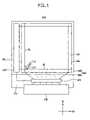
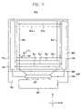
- FIG. 1is a schematic plan view showing an LCD apparatus according to an exemplary embodiment of the present invention.
- An LCD apparatus 500includes an LCD panel 300 , a gate driving circuit 350 , a data driving chip 370 and a Flexible Printed Circuit Board (FPC) 400 .
- the LCD panel 300includes a first substrate 100 , a second substrate 200 facing the first substrate 100 and a liquid crystal layer (not shown) interposed between the first and second substrates 100 and 200 .
- the LCD panel 300includes a display area DA to display an image and first to third peripheral areas PA 1 -PA 3 adjacent to the display area DA.
- the display area DAincludes pixel matrix having a plurality of gate line GL n arranged in a first direction D 1 , a plurality of data line DL m arranged in a second direction D 2 substantially perpendicular to the first direction D 1 and insulated from the gate line GL n , and a plurality of thin film transistors (TFT) 110 connected between the gate lines GL n and data lines DL m .
- TFTthin film transistors
- “n” and “m”are an integer identical to or greater than one.
- Each TFT 110includes a gate electrode connected to each gate line GL, a source electrode (a first current electrode) connected to each data line DL and a drain electrode (or a second current electrode) connected to a liquid crystal capacitor Clc.
- the gate driving circuit 350is disposed on the first peripheral area PA, and outputs gate driving signals to the gate lines GL n .
- the data driving chip 370is mounted onto the third peripheral area PA 3 and outputs a data signal to the data lines DL m .
- the FPC 400is further mounted on the third peripheral area PA 3 , in order to connect an external device (not shown) for driving the LCD panel 300 to the data driving chip 370 .
- the FPC 400provides a data signal, a data control signal and a gate control signal with the data driving chip 370 .
- the data driving chip 370outputs the data signal to the data lines DL m as well as provides the gate control signals to the gate driving circuit 350 .
- the gate driving circuit 350outputs the gate driving signals to the gate lines GL n .
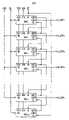
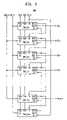
- FIG. 2is a circuit diagram showing the gate driving circuit shown in FIG. 1 .
- the gate driving circuit 350includes a shift register having a plurality of stages SRC 1 -SRC n+1 connected to one other in parallel.
- the stagesinclude an N number of driving stages SRC 1 -SRC n and one dummy stage SRC n+1 .
- Each of the stages SRC 1 to SRC n+1includes a clock signal terminal CK, a first output terminal GOUT, a second output terminal SOUT, an input terminal IN and a control terminal CT.
- Nin an integer identical to or greater than one.
- First and second clock signals CK and CKBhaving an opposite phase to each other, are alternatively applied to the clock signal terminals CK of the stages.
- the first clock signal CKis applied to the odd-numbered stages SRC 1 , SRC 3 , . . . , SRC n+1 of the stages.
- the second clock signal CKBis applied to the even-numbered stages SRC 2 , SRC 4 , . . . , SRC n of the stages.
- the first output terminal GOUTIn response to the first or second clock signal CK or CKB, the first output terminal GOUT outputs the first or second clock signal CK or CKB as a gate driving signal, which is applied to a corresponding one of the gate lines GL n , and the second output terminal SOUT outputs the first or second clock signal CK or CKB as a stage driving signal.
- the input terminal INreceives the stage driving signal output from the second output terminal SOUT of a previous stage
- the control terminal CTreceives the stage driving signal output from the second output terminal SOUT of a next stage.
- the input terminal IN of the first driving stage SRC 1receives a start signal ST because there is no previous stage with respect to the first driving stage SRC 1 .
- the control terminal CT of the dummy stage SRC n+1receives the start signal ST because there is no next stage with respect to the dummy stage SRC n+1 .
- Each of the stages SRC 1 to SRC n+1further includes a ground voltage terminal VSS and a driving voltage terminal VDD that receive a ground voltage and a driving voltage, respectively.
- FIG. 3is a timing diagram of the gate driving circuit of FIG. 2 .
- the first and second clock signals CK and CKBhave the opposite phase to each other, for example, a high state or a low state.
- the first driving stage SRC 1is activated in response to the high state of the start signal ST, and outputs a first gate driving signal G_OUT 1 of a high state through the first output terminal GOUT. Since a first gate line GL 1 connected to the first output terminal GOUT, and the TFT 110 and liquid crystal capacitor Clc connected to the first gate line GL 1 operate as a load, the first gate driving signal G_OUT 1 is delayed.
- the first driving stage SRC 1outputs a first stage driving signal S_OUT 1 of a high state through the second output terminal SOUT.
- the first stage driving signal S_OUT 1is outputted without delay because the load of the second output terminal SOUT of the first driving stage SRC 1 is relatively small.
- the first stage driving signal S_OUT 1is provided to the input terminal IN of a second driving stage SRC 2 , so that the second driving stage SRC 2 is operated regardless of the delay of the first gate driving signal G_OUT 1 .
- the second driving stage SRC 2outputs a second gate driving signal G_OUT 2 of a high state and a second stage driving signal S_OUT 2 of a high stage through a first output terminal GOUT and a second output terminal SOUT thereof, respectively.
- the second stage driving signal S_OUT 2is provided to the control terminal CT of the first driving stage SRC 1 and to the input terminal IN of a third driving stage SRC 3 . Therefore, the first gate driving signal G_OUT, and the first stage driving signal S_OUT 1 respectively output from the first and second output terminals GOUT and SOUT of the first driving stage SRC 1 are transitioned into a low state in response to the second stage driving signal S_OUT 2 .
- the third driving stage SRC 3outputs a third gate driving signal G_OUT 3 and a third stage driving signal S_OUT 3 having a high stage through first and second output terminals GOUT and SOUT, respectively, while the second gate driving signal G_OUT 2 and second stage driving signal S_OUT 2 output from the first and second output terminals GOUT and SOUT of the second driving stage SRC 2 transition from a high stage to a low state.
- the gate driving signal in a high stateis sequentially output from the driving stages SRC 1 to SRC_O n .
- FIG. 4is a circuit diagram showing each stage of FIG. 2 .
- Each stage of the stages of the gate driving circuit 350includes a first pull-up part 351 , a second pull-up part 352 , a first pull-down part 353 , a second pull-down part 354 , a pull-up driving part 355 and a pull-down driving part 356 .
- the first pull-up part 351transmits the first clock signal CK or the second clock signal CKB from the clock signal terminal CK to the first output terminal GOUT.
- the second pull-up part 352transmits the first clock signal CK or the second clock signal CKB from the clock signal terminal CK to the second output terminal SOUT.
- the first pull-up part 351includes a first NMOS transistor NT 1 having a gate electrode connected to a first node N 1 , a source electrode connected to the clock signal terminal CK and a drain electrode connected to the first output terminal GOUT.
- the second pull-up part 352includes a second NMOS transistor NT 2 having a gate electrode connected to the gate electrode of the first NMOS transistor NT 1 , a source electrode connected to the clock signal terminal CK and a drain electrode connected to the second output terminal SOUT.
- the first and second NMOS transistors NT 1 and NT 2each have a channel length of about 3.5 micrometers.
- the first NMOS transistor NT 1has a channel width of about 1110 micrometers and the second NMOS transistor NT 2 has a channel width of about 100 micrometers.
- the channel width ratio of the first NMOS transistor NT 1 to the second NMOS transistor NT 2is approximately 10:1.
- the first pull-down part 353is activated in response to the inactivation of the first pull-up part 351 , and discharges the first clock signal CK or second clock signal CKB output from the first output terminal GOUT.
- the second pull-down part 354is activated in response to the inactivation of the second pull-up part 352 , and discharges the first clock signal CK or second clock signal CKB output from the second output terminal SOUT.
- the first pull-down part 353includes a third NMOS transistor NT 3 having a gate electrode connected to a second node N 2 , a drain electrode connected to the first output terminal GOUT and a source electrode connected to the ground voltage terminal VSS.
- the second pull-down part 354includes a fourth NMOS transistor NT 4 having a gate electrode connected to the gate electrode of the third NMOS transistor NT 3 , a drain electrode connected to the second output terminal SOUT and a source electrode connected to the ground voltage terminal VSS.
- the third and fourth NMOS transistors NT 3 and NT 4each have a channel length of about 3.5 micrometers.
- the third NMOS transistor NT 3has a channel width of about 2035 micrometers and the fourth NMOS transistor NT 4 has a channel width of about 100 micrometers, so that a channel width ratio of the third NMOS transistor T 3 to the fourth NMOS transistor T 4 is approximately 20:1.
- the pull-up driving part 355includes fifth, sixth and seventh NMOS transistors NT 5 , NT 6 and NT 7 and activates the first and second pull-up parts 351 and 352 .
- the fifth NMOS transistor NT 5includes a gate electrode connected to the input terminal IN, a drain electrode connected to the driving voltage terminal VDD and a source electrode connected to the first node N 1 .
- the sixth NMOS transistor NT 6includes gate and drain electrodes commonly connected to the driving voltage terminal VDD, and a source electrode connected to the third node N 3 .
- the seventh NMOS transistor NT 7includes a gate electrode connected to the first node N 1 , a drain electrode connected to the third node N 3 and a source electrode connected to the ground voltage terminal VSS.
- the fifth, sixth and seventh NMOS transistors NT 5 , NT 6 and NT 7each have a channel length of about 3.5 micrometers.
- the fifth NMOS transistor NT 5has a channel width of about 300 micrometers, and the sixth and seventh NMOS transistors NT 6 and NT 7 each have a channel width of about 50 micrometers.
- the pull-down driving part 356includes eighth, ninth, tenth and eleventh NMOS transistors NT 8 , NT 9 , NT 10 and NT 11 and inactivates the first and second pull-up parts 351 and 352 . Further, the pull-down driving part 356 activates the first and second pull-down part 353 and 354 .
- the eighth NMOS transistor NT 8includes a gate electrode connected to a third node N 3 , a drain electrode connected to the driving voltage terminal VDD and a source electrode connected to the second node N 2 .
- the ninth NMOS transistor NT 9includes a gate electrode connected to the first node N 1 , a drain electrode connected to the second node N 2 and a source electrode connected to the ground voltage terminal VSS.
- the tenth NMOS transistor NT 10includes a gate electrode connected to the second node N 2 , a drain electrode connected to the first node N 1 and a source electrode connected to the ground voltage terminal VSS.
- the eleventh NMOS transistor NT 11includes a gate electrode connected to the control terminal CT, a drain electrode connected to the first node N 1 and a source electrode connected to the ground voltage terminal VSS.
- the pull-down driving part 356further includes a twelfth NMOS transistor NT 12 includes a gate electrode connected to the input terminal IN, a drain electrode connected to the second node N 2 and a source electrode connected to the ground voltage terminal VSS.
- the eighth, ninth, tenth, eleventh and twelfth NMOS transistors NT 8 , NT 9 , NT 10 , NT 11 and NT 12have a channel length of about 3.5 micrometers.
- the eight and twelfth NMOS transistors NT 8 and NT 12have a channel width of about 100 micrometers.
- the ninth, ten and eleventh NMOS transistors NT 9 , NT 10 and NT 11have a channel width of about 150 micrometers, about 100 micrometers and about 150 micrometers, respectively.
- the fifth NMOS transistor NT 5When the input terminal IN receives a stage driving signal from the second output terminal SOUT of a previous stage, the fifth NMOS transistor NT 5 is activated to raise an electric potential at the first node N 1 .
- the first and second NMOS transistors NT 1 and NT 2are activated to output the gate driving signal and the stage driving signal via the first output terminal GOUT and the second output terminal SOUT, respectively.
- the seventh NMOS transistor NT 7is activated in response to the electric potential of a high level at the first Node N 1 . Since the seventh NMOS transistor NT 7 is activated and the sixth NMOS transistor NT 6 maintains an activation state, an electric potential falls down at the third node N 3 .
- the eighth NMOS transistor T 8is inactivated, and thus, the second node N 2 does not receive the driving voltage VDD.
- the ninth NMOS transistor NT 9is activated in response to the electric potential of a high level at the first node N 1 so that the electric potential at the second node N 2 is maintained in the ground voltage VSS.
- the third and fourth NMOS transistors NT 3 and NT 4are inactivated.
- the eleventh NMOS transistor T 11When the control terminal CT receives the stage driving signal from the second output terminal SOUT of a next stage, the eleventh NMOS transistor T 11 is activated to discharge the electric potential at the first node N 1 to the ground voltage VSS. In response to the electric potential of a low level at the first note N 1 , the seventh and ninth NMOS transistors NT 7 and NT 9 are inactivated. Thus, the electric potential at the second node N 2 is gradually raised in response to the activation of the eighth NMOS transistor NT 8 , and the third and fourth NMOS transistors NT 3 and NT 4 are activated to discharge the gate driving signal output from the first and second output terminals GOUT and SOUT to the ground voltage VSS.
- each stagemay output the gate and stage driving signals, which maintain a high state during a predetermined period.
- FIG. 5is a diagram showing the data driving chip 370 connected to the gate driving circuit 350 .
- the data driving chip 370includes a start signal input terminal STT to receive a start signal ST, a first clock signal input terminal CKT to receive a first clock signal CK, a second clock signal input terminal CKBT to receive a second clock signal CKB, a ground voltage input terminal VSST to receive a ground voltage VSS and a driving voltage input terminal VDDT to receive a driving voltage VDD.
- the start signal input terminal STTis electrically connected to the first driving stage SRC 1 and dummy stage SRC n+1 of the gate driving circuit 350 .
- the first clock signal input terminal CKTis electrically connected to the clock signal terminal CK of the odd numbered stages SRC 1 , SRC 3 , . . . SRC n+1
- the second clock signal input terminal CKBTis electrically connected to the clock signal terminal CK of the even numbered stages SRC 2 , SRC 4 , . . . SRC n .
- the ground voltage input terminal VSSTis electrically connected to the ground voltage terminal VSS of the stages SRC 1 , . . . , SRC n+1 .
- the driving voltage input terminal VDDTis electrically connected to the driving voltage terminal VDD of the stages SRC_O 1 , . . . , SRC_O n+1 .
- the data driving chip 370provides the start signal ST, the first and second clock signals CK and CKB, the ground voltage CSS and the driving voltage VDD with the gate driving circuit 350 .
- FIG. 6is a schematic plan view showing an organic electro-luminescent display apparatus, according to another exemplary embodiment of the present invention.
- An organic electro-luminescent (EL) display apparatus 700includes an organic electro-luminescent display panel 600 having a first substrate 100 , a second substrate 200 facing the first substrate 100 and an organic electro-luminescent device (EL) interposed between the first and second substrates 100 and 200 .
- ELorganic electro-luminescent device
- the organic electro-luminescent display panel 600includes a display area DA for displaying an image and first and third peripheral areas PA 1 to PA 3 adjacent to the display area DA.
- the display area DAincludes a plurality of pixels formed in a matrix configuration, an N number of gate lines GLs arranged in a first direction D 1 and an M number of data lines DL arranged in a second direction D 2 substantially perpendicular to the first direction D 1 and insulated from the gate lines GLs.
- N and “M”are an integer identical to greater than one.
- Each of the pixelsis defined by the gate line GL, the data line DL and a power supply line PSL, and includes a switching transistor 110 , a driving transistor 120 , an organic electro-luminescent device (EL).
- the switching transistor 110includes a source electrode connected to the data line DL, a gate electrode connected to the gate line GL and a drain electrode connected to both a liquid crystal capacitor Clc and the gate electrode of the driving transistor 120 .
- the driving transistor 120includes a source electrode electrically connected to the power supply line PSL, a drain electrode connected to the organic electro-luminescent device (EL) and a gate electrode connected to the drain electrode of the switching transistor 110 .
- the liquid crystal capacitor Clcis electrically connected between the drain electrode of the switching transistor 110 and the source electrode of the driving transistor 120 .
- the organic electro-luminescent deviceincludes a grounded cathode electrode and an anode electrode connected to the drain electrode of the driving transistor 120 so as to receive the driving current provided from the power supply line PSL.
- the power supply line PSLreceives a direct current signal from an external power supply device (not shown).
- a gate driving circuit 350is disposed onto the first peripheral area PA 1 to sequentially output gate driving signals to the gate lines GL.
- a data driving chip 370is mounted onto the third peripheral area PA 3 to output a data signal to the data lines DL.
- An external device(not shown) for driving the LCD panel 300 and a Flexible Printed Circuit board (FPC) 400 for electrically connecting the external device to the LCD panel 300 may be further mounted onto the third peripheral area PA 3 .
- the FPC 400is electrically connected to the data driving chip 370 to output a data signal, a data control signal and a gate control signal.
- the gate control signalis applied to the gate driving circuit 350 through the data driving chip 370 .
- the gate driving circuit 350includes a plurality of stages. Each stage includes a clock signal terminal to receive a clock signal, a first output terminal to output the clock signal as a gate driving signal, a second output terminal to output the clock signal as a stage driving signal, an input terminal and a control terminal to receive the stage driving signal.
- the stage driving signalis provided to the input and control terminals of the adjacent stages without distorting.
- the operational properties of the gate driving circuit 350 and the display properties of the display apparatus 700are improved.
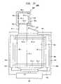
- FIG. 7is a schematic plan view showing an LCD apparatus according to another exemplary embodiment of the present invention.
- the same reference numeralsare used to refer the same or like parts those described in FIG. 1 and any further explanation is omitted.
- An LCD apparatus 800includes an LCD panel 300 , first and second gate driving circuits 350 and 360 , a data driving chip 370 and a Flexible Printed Circuit board (FPC) 400 .
- the LCD panel 300includes a first substrate 100 , a second substrate 200 facing the first substrate 100 and a liquid crystal layer (not shown) interposed between the first and second substrates 100 and 200 .
- the first gate driving circuit 350is disposed on the first peripheral area PA, and outputs gate driving signals to the odd numbered gate lines of the gate lines GL 2n ⁇ 1 .
- the second gate driving circuit 360is disposed on the second peripheral area PA 2 , which is opposite the first peripheral area PA 1 , and outputs the gate driving signals to the even numbered gate lines of the gate lines GL 2n .
- the data driving chip 370is mounted onto the third peripheral area PA 3 and outputs a data signal to the data lines DL m .
- the FPC 400is further mounted. The FPC 400 electrically connects an external device (not shown) for driving the LCD panel 300 and the data driving chip 370 .
- the data driving chip 370outputs a data signal and first and second gate control signals to the data lines DL m and the first and second gate driving circuits 350 and 360 through the FPC 400 . Therefore, the first and second gate driving circuits 350 and 360 apply the gate driving signals to the odd numbered and even numbered gate lines of the gate lines, respectively.
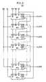
- FIG. 8is a circuit diagram showing the first gate driving circuit shown in FIG. 7 .
- the first gate driving circuit 350includes a first shift register having a plurality of odd stages SRC_O 1 -SRC_O n+1 connected to one another in parallel. Each odd stage includes the same structure to that of the stage shown in FIG. 4 .
- the odd stagesinclude an N number of driving stages SRC_O 1 -SRC_O n and one dummy stage SRC_O n+1 .
- Each of the odd stages SRC_O 1 to SRC_O n+1includes a clock signal terminal CK, a first output terminal GOUT, a second output terminal SOUT, an input terminal IN and a control terminal CT.
- First and second clock signals CK_O and CKB_Oare alternatively applied to the clock signal terminals CK of the odd stages.
- the first clock signal CK_Ois applied to the odd-numbered stages SRC_O 1 , SRC_O 3 , . . . , SRC_O n+1 of the odd stages
- the second clock signal CKB_Ois applied to the even-numbered stages SRC_O 2 , SRC_O 4 , . . . SRC_O n of the odd stages.
- the first clock signal CK_Ois outputted as a first gate driving signal through the first output terminal GOUT of the odd-numbered stages SRC_O 1 , SRC_O 3 , . . . , SRC_O n ⁇ 1 of the driving stages
- the second clock signal CKB_Ois outputted as the first gate driving signal through the first output terminal GOUT of the even-numbered stages SRC_O 2 , SRC_O 4 , . . . , SRC_O n of the driving stages.
- the first output terminal GOUT of the dummy stage SRC_O n+1is maintained in a floating state because there is no gate line corresponding to the first output terminal GOUT of the dummy stage SRC_O n+1 .
- the first output terminal GOUT of the odd stages SRC_O 1 to SRC_O nis electrically connected to a corresponding one of the odd-numbered gate lines GL 1 , GL 3 , . . . , GL 2 n ⁇ 1 formed at a display area DA. Therefore, the first gate driving signals output from the first output terminals GOUT of the odd stages SRC_O 1 to SRC_O n are sequentially applied to the odd-numbered gate lines GL 1 , GL 3 , . . . , GL 2n ⁇ 1 .
- the first clock signal CK_Ois outputted as a first stage driving signal through the second output terminal SOUT of the odd-numbered stages SRC_O 1 , SRC_O 3 , . . . , SRC_O n+1 of the odd stages
- the second clock signal CKB_Ois outputted as the first stage driving signal through the second output terminal SOUT of the even stages SRC_O 2 , SRC_O 4 , . . . SRC_O n .
- the input terminal INreceives the first stage driving signal output from the second output terminal SOUT of a previous odd stage
- the control terminal CTreceives the first stage driving signal output from the second output terminal SOUT of a next odd stage.
- the input terminal IN of the first driving stage SRC_O 1receives a first start signal ST because there is no previous odd stage with respect to the first driving stage SRC_O 1 .
- the control terminal CT of the dummy stage SRC_O n+1receives the first start signal ST because there is no next odd stage with respect to the dummy stage SRC_O n+1 .
- Each of the odd stages SRC_O 1 to SRC_O n+1further includes a ground voltage terminal VSS and a driving voltage terminal VDD that receive a ground voltage and a driving voltage, respectively.
- a second gate driving circuit 360includes a second shift register having a plurality of even stages SRC_E 1 to SRC_E n+1 connected to one another in parallel.
- the even stages SRC_E 1 to SRC_E n+1include a plurality of driving stages SRC_E 1 to SRC_E n and one dummy stage SRC_E n+1 .
- Each even stageincludes the same structure to that of the stage shown in FIG. 4 .
- Each of the even stages SRC_E 1 to SRC_E n+1includes a clock signal terminal CK, a first output terminal GOUT, a second output terminal SOUT, an input terminal IN and a control terminal CT.
- the clock signal terminal CKreceives a third clock signal CK_E or a fourth clock signal CKB_E.
- the clock signal terminal CK at the odd-numbered stages SRC_E 1 , SRC_E 3 , . . . , SRC_E n+1 of the even stagesreceives the third clock signal CK_E
- the clock signal terminal CK at the even-numbered stages SRC_E 2 , SRC_E 4 , . . . , SRC_E n of the even stagesreceives the fourth clock signal CKB_E.
- the third clock signal CK_Eis outputted as a second gate driving signal through the first output terminal GOUT of the even-numbered stages SRC_E 1 , SRC_E 3 , . . . , SRC_E n ⁇ 1 of the driving stages, and the second clock signal CKB_E is outputted as the second gate driving signal through the first output terminal GOUT of the even-numbered stages SRC_E 2 , SRC_E 4 , . . . , SRC_E n of the driving stages.
- the first output terminal GOUT of the even stages SRC_E 1 to SRC_E nis electrically connected to a corresponding one of the even-numbered gate lines GL 2 , GL 4 , . . .
- the second gate driving signals output from the first output terminals GOUT of the even stages SRC_E 1 to SRC_E nare sequentially applied to the even-numbered gate lines GL 2 , GL 4 , . . . GL 2n .
- the third clock signal CK_Eis outputted as a second stage driving signal through the second output terminal SOUT of the even-numbered stages SRC_E 1 , SRC_E 3 , . . . , SRC_E n+1 of the even stages
- the fourth clock signal CKB_Eis outputted as the second stage driving signal through the second output terminal SOUT of the even-numbered stages SRC_E 2 , SRC_E 4 , . . . , SRC_E n of the even stages.
- the second stage driving signal output from the second output terminal SOUT of a previous even stageis inputted to the input terminal IN
- the second stage driving signal output from the second output terminal SOUT of a next even stageis inputted to the control terminal CT.
- the input terminal IN of the first even stage SRC_E 1receives a second start signal ST_E because there is no previous even stage with respect to the first even stage SRC_E 1 . Also, the control terminal CT of the dummy stage SRC_E n+1 receives the second start signal ST_E since there is no next even stage with respect to the dummy stage SRC_E n+1 .
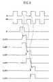
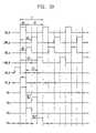
- FIG. 10is a timing diagram of the first and second gate driving circuits shown in FIGS. 8 and 9 .
- the first, second, third and fourth clock signals CK_O, CKB_O, CK_E and CKB_Eeach have a high state or a low state during a predetermined period T such that only one clock signal of a high state exists during a quarter period 1 ⁇ 4T. Therefore, each of the first, second, third and fourth clock signals CK_O, CKB_O, CK_E and CKB_E has a high state during a first quarter period 1 ⁇ 4T and a low state during the last periods, that is, three quarter period 3 ⁇ 4T.
- the second to third clock signals CKB_O, CK_E and CKB_Eare delayed with respect to the first clock signal CK_O.
- the second clock signal CKB_Ois delayed by a half period 1 ⁇ 2T with respect to the first clock signal CK_O
- the third clock signal CK_Eis delayed by a quarter period 1 ⁇ 4T with respect to the first clock signal CK_O
- the fourth clock signal CKB_Eis delayed by a three quarter period 3 ⁇ 4T with respect to the first clock signal CK_O.
- a first odd stage SRC_O 1In response to the transition of a first start signal ST_O from a high state to a low state, a first odd stage SRC_O 1 outputs the first clock signal CK_O of a high state as a first gate driving signal, which is applied to a first gate line GL 1 .
- the second start signal ST_Eis delayed by a quarter period 1 ⁇ 4T with respect to the first start signal ST_O, but is ahead by a quarter period 1 ⁇ 4T with respect to the third clock signal CK_E.
- a first even stage SRC_E 1When the second start signal ST_E is transitioned from a high state to a low state, a first even stage SRC_E 1 outputs the third clock signal CK_E of a high state as a second gate driving signal, which is applied to a second gate line GL 2 .
- the second gate driving signalis applied to the even-numbered gate line GL 2 , after the first gate driving signal applied to the odd-numbered gate line GL 1 is transitioned from a high state to a low state.
- a second odd stage SRC_O 2When the second clock signal CKB_O of a high state is applied to the first gate driving circuit 350 in response to the transition of the first clock signal CK_O from a high state to a low state, a second odd stage SRC_O 2 outputs the second clock signal CKB_O of a high state as the first gate driving signal in response to the first stage driving signal output from the first odd stage SRC_O 1 .
- the first gate driving signal output from the second odd stage SRC_O 2is applied to a third gate line GL 3 .
- a first blank interval BL 1exists after the first odd stage SRC_O 1 outputs the first gate driving signal of a high state and before the second odd stage SRC_O 2 outputs the first gate driving signal of a high state.
- the second even stage SRC_E 2When the fourth clock signal CKB_E of a high state is applied to a second even stage SRC_E 2 after the third clock signal CK_E is transitioned from a high state to a low state, the second even stage SRC_E 2 outputs the fourth clock signal CKB_E of a high state as the second gate driving signal in response to the second stage driving signal output from the first even stage SRC_E 1 .
- the second gate driving signal output from the second even stage SRC_E 2is applied to the fourth gate line GL 4 .
- a second blank interval BL 2exists after the first even stage SRC_E 1 outputs the second gate driving signal having a high state and before the second even stage SRC_E 2 outputs the second gate driving signal having a high state.
- the N number of odd stages SRC_O 1 to SRC_O n and the N number of even stages SRC_E 1 to SRC_E nare alternately activated to output the first and second gate driving signals, which are alternatively applied to the gate lines GL 1 to GL 2n .
- FIG. 11is a timing diagram of the first and second gate driving circuits according to another exemplary embodiment of the present invention.
- the first to fourth clock signals CK_O, CKB_O, CK_E and CKB_Eeach have a high state or a low state during a predetermined period T.
- the clock signalseach have a high state during a first half period 1 ⁇ 2T and a low state during the last half period 1 ⁇ 2T.
- the second clock signal CKB_Ois delayed by a half period 1 ⁇ 2T with respect to the first clock signal CK_O, and thus the first and second clock signals CK_O and CKB_O have the opposite phase to each other during the predetermined period T.
- the third clock signal CK_Eis delayed by a quarter period 1 ⁇ 4T with respect to the first clock signal CK_O and the fourth clock signal CKB_E is delayed by a half period 1 ⁇ 2T with regard to the third clock signal CK_E.
- the third and fourth clock signals CK_E and CKB_Ehave the opposite phase to each other during the predetermined period T.
- a first start signal ST_Ohas a high state during a half period 1 ⁇ 2T and is transitioned from a high state to a low state before the first clock signal CK_O of a high state is applied to a first odd stage SRC_O 1 .
- the first odd stage SRC_O 1outputs the first clock signal CK_O having a high state as a first gate driving signal, which is applied to a first gate line GL 1 .
- the second odd stage SRC_O 2When the second clock signal CKB_O is applied to a second odd stage SRC_O 2 after the first clock signal CK_O is transitioned from a high state to a low state, the second odd stage SRC_O 2 outputs the second clock signal CKB_O of the high state as the first gate driving signal, in response to the first stage driving signal output from the first odd stage SRC_O 1 , which is applied to a third gate line GL 3 .
- a second start signal ST_Eis delayed by a quarter period 1 ⁇ 4T with the first start signal ST_O and has a high state during a half period 1 ⁇ 2T.
- a first even stage SRC_E 1outputs the third clock signal CK_E of a high state as a second gate driving signal, which is applied to a second gate line GL 2 .
- the second even stage SRC_E 2When the fourth clock signal CKB_E of a high state is applied to a second even stage SRC_E 2 after the third clock signal CK_E is transitioned from a high state to a low state, the second even stage SRC_E 2 outputs the fourth clock signal CKB_E of a high state as the second gate driving signal in response to a second stage driving signal output from the first even stage SRC_E 1 .
- the second gate driving signal output from the second even stage SRC_E 2is applied to a fourth gate line GL 4 .
- the first gate driving signal output from the first or second odd stage SRC_O 1 or SRC_O 2has a first dummy interval D 1 during a quarter period 1 ⁇ 4T and a first active interval A 1 following the first dummy interval D 1 during a quarter period 1 ⁇ 4T.
- the second gate driving signal output from the first or second even stage SRC_E 1 or SRC_E 2has also a second dummy interval D 2 during a quarter period 1 ⁇ 4T and a second active interval A 2 following the second dummy interval D 2 during a quarter period 1 ⁇ 4T.
- the active interval A 1 of the first gate driving signal applied to the first gate line GL 1is overlapped with the dummy interval D 2 of the second gate driving signal applied to the second gate line GL 2 .
- the first gate driving signal applied to the third gate line GL 3is delayed by a quarter period 1 ⁇ 4T with respect to the second driving signal applied to the second gate line GL 2 , and thus, the active interval A 2 of the second gate driving signal applied to the second gate line GL 2 is overlapped with the dummy interval D 1 of the first gate driving signal applied to the third gate line GL 3 .
- the driving chip 370outputs a data driving signal during the first or second active period A 1 or A 2 .
- the driving chip 370outputs a first data driving signal DATA 1 at the first active interval A 1 of the first gate driving signal applied to the first gate line GL 1 and outputs a second data driving signal DATA 2 at the second active interval A 2 of the second gate driving signal applied to the second gate line GL 2 .
- the gate lines GL 1 to GL 2nalternately receive the first and second gate driving signals.
- the LCD apparatus 800Since the first gate driving circuit 350 outputting the first gate driving signal to the odd gate lines and the second gate driving circuit 360 outputting the second gate driving signal to the even gate lines are independently operated, the first and second gate driving circuits 350 and 360 are not subordinately connected to each other. Thus, the LCD apparatus 800 prevents the first and second gate driving signals from distorting due to a line resistance of the gate lines. Therefore, the LCD apparatus 800 improves its operational properties. Further, since the first and second gate driving circuits 350 and 360 are disposed on the LCD panel such that the LCD panel has a symmetric structure and the LCD panel is formed with a single chip, the LCD apparatus 800 has a reduced BM width and improved display property.
- FIG. 12is a plan view showing an LCD apparatus with dual display screen according to further exemplary embodiment of the present invention.
- An LCD apparatus with a dual display screen 1000includes a first LCD panel 300 , a second LCD panel 900 , a driving chip 370 , a first FPC 400 and a second FPC 450 .
- the first LCD panel 300includes a first display area DA 1 for displaying a first image and first, second, third and fourth peripheral areas PA 1 , PA 2 , PA 3 and PA 4 surrounding the first display area DA 1 .
- the first LCD panel 300includes a 2N number of first gate lines GL 1-1 to GL 1-2n and an M number of first data lines DL 1-1 to DL 1-m substantially perpendicular to the first gate lines GL 1-1 to GL 1-2n , at the first display area DA 1 .
- a first gate driving circuit 350is formed on the first peripheral area PA 1 and a second gate driving circuit 360 is formed on the second peripheral area PA 2 .
- the first gate driving circuit 350outputs first gate driving signals to odd-numbered gate lines of the first gate lines GL 1-1 to GL 1-2n ⁇ 1
- the second gate driving circuit 360outputs second gate driving signals to even-numbered gate lines of the first gate lines GL 1-2 to GL 1-2n .
- the driving chip 370is mounted on the third peripheral area PA 3 , to which the first FPC 400 is attached.
- the first FPC 400is electrically connected to the driving chip 370 to apply external signals to the driving chip 370 .
- the driving chip 370outputs the first data signal to the first data lines DL 1-1 to DL 1-m , and outputs first and second gate control signals to the first and second gate driving circuits 350 and 360 , respectively.
- the first and second gate driving circuits 350 and 360output first and second gate driving signals to the first gate lines GL 1-1 to GL 1-2n .
- the second LCD panel 900includes a second display area DA 2 for displaying a second image, and fifth and sixth peripheral areas PA 5 and PA 6 adjacent to the second display area DA 2 .
- a third gate driving circuit 910is formed on the sixth peripheral area PA 6 .
- the second LCD panel 900includes a I number of second gate lines GL 2-1 to GL 2-i and a J number of second data line DL 2-1 to DL 2-j substantially perpendicular to the second gate lines GL 2-1 to GL 2-I , at the second display area DA 2 .
- the driving chip 370outputs the second data signal to the second LCD panel 900 and a third gate control signal to the third gate driving circuit 910 .
- the third gate driving circuit 910sequentially outputs a third gate driving signal to the second gate lines GL 2-1 to GL 2-i in response to the third gate control signal.
- the data signalis applied to second data lines DL 2-1 to DL 2-j
- the third gate driving signalis applied to the second gate lines GL 2-1 to GL 2-i .
- the “I” and “N”are an integer identical to or greater than two, and the “I” is equal to or less than the “N”.
- the “J” and “M”are an integer identical to or greater than two, and the “J” is equal to or less than the “M”.
- the first and second LCD panels 300 and 900are electrically connected to each other by means of the second FPC 450 .
- the second FPC 450includes a first end portion attached to the fourth peripheral area PA 4 of the first LCD panel 300 and a second end portion attached to the fifth peripheral area PA 5 of the second LCD panel 900 .
- the driving chip 370is electrically connected to the second LCD panel 900 by means of the second FPC 450 .
- One end of the first data lines DL 1-1 to DL 1-jis electrically connected to the second data line DL 2-1 to DL 2-j via a connection line CL 1-1 to CL 1-j formed at the second FPC 450 .
- the second data signal output from the driving chip 370is applied to the second data line DL 2-1 to DL 2-j via the connection line CL 1-1 to CL 1-j .
- FIG. 12shows an LCD apparatus in which two gate driving circuits 350 and 360 are connected to the first LCD panel 300
- the LCD apparatusmay include one gate driving circuit to output gate driving signals to the first gate lines of the first LCD panel 300 .
Landscapes
- Engineering & Computer Science (AREA)
- Chemical & Material Sciences (AREA)
- Crystallography & Structural Chemistry (AREA)
- Physics & Mathematics (AREA)
- Computer Hardware Design (AREA)
- General Physics & Mathematics (AREA)
- Theoretical Computer Science (AREA)
- Control Of Indicators Other Than Cathode Ray Tubes (AREA)
- Shift Register Type Memory (AREA)
- Liquid Crystal Display Device Control (AREA)
Abstract
Description
Claims (33)
Priority Applications (5)
| Application Number | Priority Date | Filing Date | Title |
|---|---|---|---|
| US12/050,442US8085235B2 (en) | 2003-04-29 | 2008-03-18 | Gate driving circuit and display apparatus having the same |
| US13/307,440US9269317B2 (en) | 2003-04-29 | 2011-11-30 | Gate driving circuit and display apparatus having the same |
| US14/994,739US10283070B2 (en) | 2003-04-29 | 2016-01-13 | Gate driving circuit and display apparatus having the same |
| US16/398,986US10847111B2 (en) | 2003-04-29 | 2019-04-30 | Gate driving circuit and display apparatus having the same |
| US17/091,317US11361728B2 (en) | 2003-04-29 | 2020-11-06 | Gate driving circuit and display apparatus having the same |
Applications Claiming Priority (4)
| Application Number | Priority Date | Filing Date | Title |
|---|---|---|---|
| KR1020030027087AKR100930491B1 (en) | 2003-04-29 | 2003-04-29 | Gate drive circuit and liquid crystal display device having the same |
| KR2003-27087 | 2003-04-29 | ||
| KR2003-81525 | 2003-11-18 | ||
| KR1020030081525AKR100976986B1 (en) | 2003-11-18 | 2003-11-18 | Gate driving circuit and display device having same |
Related Child Applications (2)
| Application Number | Title | Priority Date | Filing Date |
|---|---|---|---|
| US12/050,442DivisionUS8085235B2 (en) | 2003-04-29 | 2008-03-18 | Gate driving circuit and display apparatus having the same |
| US13/307,440DivisionUS9269317B2 (en) | 2003-04-29 | 2011-11-30 | Gate driving circuit and display apparatus having the same |
Publications (2)
| Publication Number | Publication Date |
|---|---|
| US20040217935A1 US20040217935A1 (en) | 2004-11-04 |
| US7369111B2true US7369111B2 (en) | 2008-05-06 |
Family
ID=33312685
Family Applications (6)
| Application Number | Title | Priority Date | Filing Date |
|---|---|---|---|
| US10/832,631Active2025-10-30US7369111B2 (en) | 2003-04-29 | 2004-04-27 | Gate driving circuit and display apparatus having the same |
| US12/050,442Active2026-11-13US8085235B2 (en) | 2003-04-29 | 2008-03-18 | Gate driving circuit and display apparatus having the same |
| US13/307,440Expired - LifetimeUS9269317B2 (en) | 2003-04-29 | 2011-11-30 | Gate driving circuit and display apparatus having the same |
| US14/994,739Expired - LifetimeUS10283070B2 (en) | 2003-04-29 | 2016-01-13 | Gate driving circuit and display apparatus having the same |
| US16/398,986Expired - Fee RelatedUS10847111B2 (en) | 2003-04-29 | 2019-04-30 | Gate driving circuit and display apparatus having the same |
| US17/091,317Expired - LifetimeUS11361728B2 (en) | 2003-04-29 | 2020-11-06 | Gate driving circuit and display apparatus having the same |
Family Applications After (5)
| Application Number | Title | Priority Date | Filing Date |
|---|---|---|---|
| US12/050,442Active2026-11-13US8085235B2 (en) | 2003-04-29 | 2008-03-18 | Gate driving circuit and display apparatus having the same |
| US13/307,440Expired - LifetimeUS9269317B2 (en) | 2003-04-29 | 2011-11-30 | Gate driving circuit and display apparatus having the same |
| US14/994,739Expired - LifetimeUS10283070B2 (en) | 2003-04-29 | 2016-01-13 | Gate driving circuit and display apparatus having the same |
| US16/398,986Expired - Fee RelatedUS10847111B2 (en) | 2003-04-29 | 2019-04-30 | Gate driving circuit and display apparatus having the same |
| US17/091,317Expired - LifetimeUS11361728B2 (en) | 2003-04-29 | 2020-11-06 | Gate driving circuit and display apparatus having the same |
Country Status (2)
| Country | Link |
|---|---|
| US (6) | US7369111B2 (en) |
| TW (2) | TW201301254A (en) |
Cited By (40)
| Publication number | Priority date | Publication date | Assignee | Title |
|---|---|---|---|---|
| US20050201508A1 (en)* | 2004-03-12 | 2005-09-15 | Kyong-Ju Shin | Shift register and display device including the same |
| US20060022920A1 (en)* | 2004-07-28 | 2006-02-02 | Lg.Philips Lcd Co., Ltd. | Display device and driving method thereof |
| US20070195053A1 (en)* | 2006-02-23 | 2007-08-23 | Mitsubishi Electric Corporation | Shift register circuit and image display apparatus containing the same |
| US20070248204A1 (en)* | 2006-04-25 | 2007-10-25 | Mitsubishi Electric Corporation | Shift register circuit and image display apparatus equipped with the same |
| US20070247932A1 (en)* | 2006-04-25 | 2007-10-25 | Mitsubishi Electric Corporation | Shift register circuit and image display comprising the same |
| US20080080661A1 (en)* | 2006-10-03 | 2008-04-03 | Mitsubishi Electric Corporation | Shift register circuit and image display apparatus containing the same |
| US20080143759A1 (en)* | 2006-12-14 | 2008-06-19 | Au Optronics Corporation | Gate Driving Circuit and Driving Circuit Unit Thereof |
| US20080150925A1 (en)* | 2006-12-26 | 2008-06-26 | Au Optronics Corporation | Gate Driving Circuit and Driving Method Thereof |
| US20080150875A1 (en)* | 2006-12-22 | 2008-06-26 | Innolux Display Corp. | Shift register and liquid crystal display using same |
| US20080219401A1 (en)* | 2007-03-05 | 2008-09-11 | Mitsubishi Electric Corporation | Shift register circuit and image display apparatus containing the same |
| US20080285705A1 (en)* | 2007-05-18 | 2008-11-20 | Au Optronics Corp. | Shift register with individual driving node |
| US20090073105A1 (en)* | 2007-09-14 | 2009-03-19 | Innolux Display Corp. | Shift register and liquid crystal display using same |
| US20090110138A1 (en)* | 2007-10-29 | 2009-04-30 | Tung-Shuan Cheng | Shift Register Circuit |
| US20090179875A1 (en)* | 2008-01-16 | 2009-07-16 | Au Optronics Corp. | Flat display and driving method thereof |
| US20100321372A1 (en)* | 2008-02-19 | 2010-12-23 | Akihisa Iwamoto | Display device and method for driving display |
| US20110013740A1 (en)* | 2009-07-14 | 2011-01-20 | Chih-Lung Lin | Shift register circuit having bi-directional transmission mechanism |
| US20110080385A1 (en)* | 2009-10-07 | 2011-04-07 | Nec Lcd Technologies, Ltd. | Shift register circuit, scanning line driving circuit, and display device |
| US20110085635A1 (en)* | 2009-10-09 | 2011-04-14 | Semiconductor Energy Laboratory Co., Ltd. | Shift register and display device and driving method thereof |
| US20110216876A1 (en)* | 2010-03-02 | 2011-09-08 | Semiconductor Energy Laboratory Co., Ltd. | Pulse signal output circuit and shift register |
| US20110216874A1 (en)* | 2010-03-02 | 2011-09-08 | Semiconductor Energy Laboratory Co., Ltd. | Pulse signal output circuit and shift register |
| US20110216875A1 (en)* | 2010-03-02 | 2011-09-08 | Semiconductor Energy Laboratory Co., Ltd. | Pulse signal output circuit and shift register |
| US8232554B2 (en) | 2010-10-29 | 2012-07-31 | Chunghwa Picture Tubes, Ltd. | Transistor array substrate |
| US20120206434A1 (en)* | 2007-11-21 | 2012-08-16 | Wintek Corporation | Shift Register |
| WO2012167143A1 (en) | 2011-06-03 | 2012-12-06 | Xoma Technology Ltd. | Antibodies specific for tgf-beta |
| USRE43850E1 (en)* | 2004-10-06 | 2012-12-11 | Onanovich Group Ag, Llc | Liquid crystal driving circuit and liquid crystal display device |
| US20130049133A1 (en)* | 2011-08-29 | 2013-02-28 | Semiconductor Energy Laboratory Co., Ltd. | Semiconductor device |
| US8515000B2 (en)* | 2010-09-01 | 2013-08-20 | Au Optronics Corp. | Shift register circuit |
| US20130243150A1 (en)* | 2011-04-21 | 2013-09-19 | Lg Display Co., Ltd. | Shift register |
| US8604846B2 (en) | 2010-12-30 | 2013-12-10 | Au Optronics Corp. | Resetting circuit |
| US20140064439A1 (en)* | 2012-07-30 | 2014-03-06 | Chengdu Boe Optoelectronics Technology Co., Ltd. | Shift Register Unit, Shift Register And Display Apparatus |
| US20140085560A1 (en)* | 2012-09-21 | 2014-03-27 | Innolux Corporation | Display device |
| US8718224B2 (en) | 2011-08-05 | 2014-05-06 | Semiconductor Energy Laboratory Co., Ltd. | Pulse signal output circuit and shift register |
| US9171640B2 (en) | 2009-10-09 | 2015-10-27 | Semiconductor Energy Laboratory Co., Ltd. | Shift register and display device |
| US9424950B2 (en) | 2013-07-10 | 2016-08-23 | Semiconductor Energy Laboratory Co., Ltd. | Semiconductor device |
| WO2016161410A2 (en) | 2015-04-03 | 2016-10-06 | Xoma Technology Ltd. | Treatment of cancer using inhibitors of tgf-beta and pd-1 |
| US9552761B2 (en) | 2010-09-09 | 2017-01-24 | Semiconductor Energy Laboratory Co., Ltd. | Semiconductor device |
| TWI659406B (en)* | 2014-04-28 | 2019-05-11 | 日商夏普股份有限公司 | Active-matrix substrate and display device including the same |
| US11133335B2 (en)* | 2006-01-07 | 2021-09-28 | Semiconductor Energy Laboratory Co., Ltd. | Semiconductor device, and display device and electronic device having the same |
| US11847973B2 (en) | 2016-06-01 | 2023-12-19 | Samsung Display Co., Ltd. | Display device capable of displaying an image of uniform brightness |
| US12062405B2 (en) | 2011-10-07 | 2024-08-13 | Semiconductor Energy Laboratory Co., Ltd. | Semiconductor device |
Families Citing this family (101)
| Publication number | Priority date | Publication date | Assignee | Title |
|---|---|---|---|---|
| ATE414314T1 (en)* | 2004-05-25 | 2008-11-15 | Samsung Sdi Co Ltd | LINE SCAN DRIVER FOR AN OLED DISPLAY |
| KR100578842B1 (en)* | 2004-05-25 | 2006-05-11 | 삼성에스디아이 주식회사 | Display device, display panel and driving method thereof |
| KR101030528B1 (en)* | 2004-05-27 | 2011-04-26 | 엘지디스플레이 주식회사 | Shift register and liquid crystal display using the same |
| JP2006011286A (en)* | 2004-06-29 | 2006-01-12 | Canon Inc | Drive device, image display device, and television device |
| KR101074402B1 (en)* | 2004-09-23 | 2011-10-17 | 엘지디스플레이 주식회사 | Liquid crystal display device and method for driving the same |
| KR100658624B1 (en)* | 2004-10-25 | 2006-12-15 | 삼성에스디아이 주식회사 | Light emitting display device and driving method thereof |
| KR101191157B1 (en)* | 2004-12-31 | 2012-10-15 | 엘지디스플레이 주식회사 | Unit for driving liquid crystal display device |
| KR101166580B1 (en)* | 2004-12-31 | 2012-07-18 | 엘지디스플레이 주식회사 | Liquid crystal display device |
| KR20060085749A (en)* | 2005-01-25 | 2006-07-28 | 삼성전자주식회사 | Display panel assembly and display device having same |
| KR101133768B1 (en)* | 2005-03-07 | 2012-04-09 | 삼성전자주식회사 | Display device |
| KR101112554B1 (en)* | 2005-04-11 | 2012-02-15 | 삼성전자주식회사 | Drive device for display device and display device including same |
| JP5154033B2 (en)* | 2005-06-07 | 2013-02-27 | 三星電子株式会社 | Display device |
| US7586476B2 (en)* | 2005-06-15 | 2009-09-08 | Lg. Display Co., Ltd. | Apparatus and method for driving liquid crystal display device |
| KR101166819B1 (en)* | 2005-06-30 | 2012-07-19 | 엘지디스플레이 주식회사 | A shift register |
| KR101162093B1 (en)* | 2005-06-30 | 2012-07-04 | 엘지디스플레이 주식회사 | Liquid crystal display device |
| KR101157981B1 (en)* | 2005-06-30 | 2012-07-03 | 엘지디스플레이 주식회사 | Display Apparatus |
| KR101189273B1 (en)* | 2005-09-07 | 2012-10-09 | 삼성디스플레이 주식회사 | Driving apparatus for display device and display device including the same |
| TWI291153B (en)* | 2005-09-26 | 2007-12-11 | Au Optronics Corp | Display panels, driving method thereof and electronic devices using the same |
| TWI319865B (en)* | 2005-12-02 | 2010-01-21 | Driving circuit of liquid crystal display | |
| KR101256921B1 (en)* | 2006-02-06 | 2013-04-25 | 삼성디스플레이 주식회사 | Gate driving unit and display apparatus having the same |
| EP1845514B1 (en)* | 2006-04-14 | 2013-10-02 | Semiconductor Energy Laboratory Co., Ltd. | Display device and method for driving the same |
| KR101296624B1 (en)* | 2006-06-26 | 2013-08-14 | 엘지디스플레이 주식회사 | Driving circuit for liquid crystal display device and method for driving the same |
| KR100746646B1 (en)* | 2006-07-11 | 2007-08-06 | 삼성전자주식회사 | Display driving circuit and liquid crystal display having the same |
| KR101272337B1 (en)* | 2006-09-01 | 2013-06-07 | 삼성디스플레이 주식회사 | Display device capable of displaying partial picture and driving method of the same |
| TW200815859A (en)* | 2006-09-19 | 2008-04-01 | Epson Imaging Devices Corp | Liquid crystal display device |
| KR101298094B1 (en)* | 2006-09-25 | 2013-08-20 | 삼성디스플레이 주식회사 | Gate driving circuit and display apparatus having the same |
| JP4932415B2 (en) | 2006-09-29 | 2012-05-16 | 株式会社半導体エネルギー研究所 | Semiconductor device |
| KR101368822B1 (en)* | 2006-10-12 | 2014-03-04 | 삼성디스플레이 주식회사 | Gate driving circuit and display apparatus having the same |
| TWI360087B (en)* | 2007-02-13 | 2012-03-11 | Au Optronics Corp | Display panel |
| CN100592425C (en)* | 2007-04-27 | 2010-02-24 | 群康科技(深圳)有限公司 | Shift register and liquid crystal display |
| CN101359511B (en)* | 2007-08-03 | 2011-04-27 | 群康科技(深圳)有限公司 | Shift register and liquid crystal display using the shift register |
| TWI366177B (en)* | 2007-08-08 | 2012-06-11 | Au Optronics Corp | Lcd display with a gate driver outputting non-overlapping scanning signals |
| TWI383351B (en)* | 2007-08-30 | 2013-01-21 | Chimei Innolux Corp | Flat display and driving method thereof |
| KR101437867B1 (en)* | 2007-10-16 | 2014-09-12 | 삼성디스플레이 주식회사 | Display device, and driving device and driving method thereof |
| JP2009128888A (en)* | 2007-11-28 | 2009-06-11 | Sanyo Electric Co Ltd | LCD drive circuit |
| KR101423235B1 (en)* | 2008-01-04 | 2014-07-25 | 삼성디스플레이 주식회사 | Pixel driving circuit and display device having same |
| TWI391902B (en)* | 2008-07-14 | 2013-04-01 | Ili Technology Corp | Driving circuit |
| KR102400984B1 (en)* | 2008-11-28 | 2022-05-24 | 가부시키가이샤 한도오따이 에네루기 켄큐쇼 | Semiconductor device, display device and electronic device including the same |
| TWI410939B (en)* | 2008-12-26 | 2013-10-01 | Au Optronics Corp | Liquid display panel driving method |
| KR20100083370A (en)* | 2009-01-13 | 2010-07-22 | 삼성전자주식회사 | Gate driving circuit and display device having the same |
| JP5484109B2 (en) | 2009-02-09 | 2014-05-07 | 三菱電機株式会社 | Electro-optic device |
| US8330702B2 (en)* | 2009-02-12 | 2012-12-11 | Semiconductor Energy Laboratory Co., Ltd. | Pulse output circuit, display device, and electronic device |
| KR100986887B1 (en)* | 2009-02-17 | 2010-10-08 | 삼성모바일디스플레이주식회사 | Light emission control line driver and organic light emitting display device using the same |
| US7979607B2 (en)* | 2009-02-27 | 2011-07-12 | Honeywell International Inc. | Cascadable high-performance instant-fall-through synchronous first-in-first-out (FIFO) buffer |
| US8872751B2 (en) | 2009-03-26 | 2014-10-28 | Semiconductor Energy Laboratory Co., Ltd. | Liquid crystal display device having interconnected transistors and electronic device including the same |
| CN102428521B (en)* | 2009-05-28 | 2015-02-18 | 夏普株式会社 | Shift Register |
| KR102661073B1 (en) | 2009-06-25 | 2024-04-29 | 가부시키가이샤 한도오따이 에네루기 켄큐쇼 | Semiconductor device |
| KR101056281B1 (en)* | 2009-08-03 | 2011-08-11 | 삼성모바일디스플레이주식회사 | Organic electroluminescent display and driving method thereof |
| KR20110013693A (en)* | 2009-08-03 | 2011-02-10 | 삼성모바일디스플레이주식회사 | Organic electroluminescent display and driving method thereof |
| TW202507679A (en)* | 2009-09-10 | 2025-02-16 | 日商半導體能源研究所股份有限公司 | Semiconductor device and display device |
| TWI420452B (en)* | 2009-09-22 | 2013-12-21 | Hannstar Display Corp | Shift register for display panel |
| KR101101105B1 (en)* | 2009-11-04 | 2012-01-03 | 삼성모바일디스플레이주식회사 | Light emission control line driver and organic light emitting display device using the same |
| KR101763660B1 (en)* | 2009-12-18 | 2017-08-01 | 가부시키가이샤 한도오따이 에네루기 켄큐쇼 | Liquid crystal display device and driving method thereof |
| WO2011096153A1 (en)* | 2010-02-05 | 2011-08-11 | Semiconductor Energy Laboratory Co., Ltd. | Display device |
| CN102763332B (en) | 2010-02-23 | 2016-04-13 | 株式会社半导体能源研究所 | Display device, semiconductor device, and their driving method |
| KR101975140B1 (en)* | 2010-03-12 | 2019-05-03 | 가부시키가이샤 한도오따이 에네루기 켄큐쇼 | Display device |
| KR101073147B1 (en)* | 2010-04-05 | 2011-10-12 | 삼성모바일디스플레이주식회사 | Touch screen panel integrated flat panel display and manufacturing method |
| KR101685590B1 (en)* | 2010-05-18 | 2016-12-13 | 삼성디스플레이 주식회사 | Three dimensional image display device |
| KR102615409B1 (en)* | 2010-05-21 | 2023-12-20 | 가부시키가이샤 한도오따이 에네루기 켄큐쇼 | Pulse output circuit, shift register, and display device |
| KR101645404B1 (en) | 2010-07-06 | 2016-08-04 | 삼성디스플레이 주식회사 | Organic Light Emitting Display |
| KR101739575B1 (en)* | 2010-09-28 | 2017-05-25 | 삼성디스플레이 주식회사 | Apparatus of scan driving and driving method thereof |
| KR101769069B1 (en)* | 2010-11-29 | 2017-08-18 | 삼성디스플레이 주식회사 | Scan drvier and drving method thereof |
| TWI426486B (en)* | 2010-12-16 | 2014-02-11 | Au Optronics Corp | Gate driving circuit on array applied to chareg sharing pixel |
| JP2012189752A (en)* | 2011-03-10 | 2012-10-04 | Japan Display East Co Ltd | Display device |
| KR101832950B1 (en)* | 2011-03-28 | 2018-04-16 | 삼성디스플레이 주식회사 | Display device |
| KR101895326B1 (en)* | 2011-05-13 | 2018-09-05 | 가부시키가이샤 한도오따이 에네루기 켄큐쇼 | Display device |
| KR20130000020A (en)* | 2011-06-22 | 2013-01-02 | 삼성디스플레이 주식회사 | Stage circuit and emission driver using the same |
| KR101878976B1 (en)* | 2011-07-07 | 2018-07-17 | 삼성디스플레이 주식회사 | Method of driving touch sensing display panel and display apparatus performing the same |
| CN102368380A (en)* | 2011-09-14 | 2012-03-07 | 深圳市华星光电技术有限公司 | Liquid crystal display panel and gate drive circuit |
| TWI497159B (en)* | 2011-11-10 | 2015-08-21 | Au Optronics Corp | Display panel |
| JP6099372B2 (en)* | 2011-12-05 | 2017-03-22 | 株式会社半導体エネルギー研究所 | Semiconductor device and electronic equipment |
| CN102708926B (en)* | 2012-05-21 | 2015-09-16 | 京东方科技集团股份有限公司 | A kind of shift register cell, shift register, display device and driving method |
| KR102011985B1 (en)* | 2012-07-23 | 2019-08-20 | 삼성디스플레이 주식회사 | Display device and driving method thereof |
| KR101992889B1 (en)* | 2012-08-08 | 2019-06-25 | 엘지디스플레이 주식회사 | Shift register |
| JP2014142457A (en)* | 2013-01-23 | 2014-08-07 | Japan Display Inc | Display device |
| CN104393025B (en)* | 2014-12-09 | 2017-08-11 | 京东方科技集团股份有限公司 | A kind of array base palte, touch-control display panel and touch control display apparatus |
| CN104658506B (en)* | 2015-03-18 | 2018-01-30 | 合肥京东方光电科技有限公司 | Shift register, gate driving circuit and its driving method, display panel |
| JP6830765B2 (en)* | 2015-06-08 | 2021-02-17 | 株式会社半導体エネルギー研究所 | Semiconductor device |
| JP6154445B2 (en)* | 2015-09-09 | 2017-06-28 | 株式会社半導体エネルギー研究所 | Display device |
| CN108496366A (en)* | 2017-03-31 | 2018-09-04 | 深圳市大疆创新科技有限公司 | Dual-screen display device, method and device, video glass, chip and processor |
| CN106898288A (en)* | 2017-04-10 | 2017-06-27 | 深圳市华星光电技术有限公司 | Display panel and display device |
| US20180293923A1 (en)* | 2017-04-10 | 2018-10-11 | Shenzhen China Star Optoelectronics Technology Co. , Ltd. | Display panel and display device |
| CN107232700A (en)* | 2017-06-12 | 2017-10-10 | 捷开通讯(深圳)有限公司 | A kind of Intelligent worn device |
| CN107068108B (en)* | 2017-06-26 | 2019-06-28 | 惠科股份有限公司 | Display panel driving method and device and display device |
| CN107492361B (en)* | 2017-09-26 | 2022-01-11 | 惠科股份有限公司 | Shift register circuit and display panel using same |
| KR102392118B1 (en)* | 2017-09-27 | 2022-04-27 | 엘지디스플레이 주식회사 | Shift register and display apparatus comprising the same |
| US10475408B2 (en)* | 2017-11-07 | 2019-11-12 | Shenzhen China Star Optoelectronics Semiconductor Display Technology Co., Ltd | Liquid crystal display panel with a polarity reversion and gate driving circuit thereof |
| KR102507830B1 (en)* | 2017-12-29 | 2023-03-07 | 엘지디스플레이 주식회사 | Display apparatus |
| TWI649733B (en)* | 2018-02-26 | 2019-02-01 | 友達光電股份有限公司 | Display device and its gate driver |
| US11571803B2 (en)* | 2019-05-30 | 2023-02-07 | Milwaukee Electric Tool Corporation | Power tool with combined chip for wireless communications and power tool control |
| WO2021031167A1 (en)* | 2019-08-21 | 2021-02-25 | 京东方科技集团股份有限公司 | Display substrate, display device, and method for fabricating display substrate |
| BR112019026794A2 (en)* | 2019-08-21 | 2022-04-12 | Boe Technology Group Co Ltd | Display substrate and method of manufacture thereof and display device |
| US11900884B2 (en) | 2019-08-21 | 2024-02-13 | Chengdu Boe Optoelectronics Technology Co., Ltd. | Display substrate having a scan driving circuit with a plurality of shift registers and manufacturing method thereof, display device |
| CN113785350B (en) | 2020-04-10 | 2023-06-16 | 京东方科技集团股份有限公司 | Display substrate, manufacturing method thereof and display device |
| WO2021203422A1 (en) | 2020-04-10 | 2021-10-14 | 京东方科技集团股份有限公司 | Display substrate and manufacturing method therefor, and display device |
| US11688339B2 (en)* | 2020-04-10 | 2023-06-27 | Chengdu Boe Optoelectronics Technology Co., Ltd. | Display substrate and manufacturing method thereof, display device |
| KR102825010B1 (en) | 2020-09-25 | 2025-06-27 | 삼성디스플레이 주식회사 | Gate driving circuit and display apparatus including the same |
| CN113112949B (en)* | 2021-04-27 | 2023-06-30 | 武汉天马微电子有限公司 | Gate driving circuit, display panel, display device and driving method |
| CN115019717B (en)* | 2022-06-29 | 2025-01-24 | 武汉华星光电半导体显示技术有限公司 | Display panel and display device |
| US11847968B1 (en) | 2022-07-12 | 2023-12-19 | Wuhan China Star Optoelectronics Semiconductor Display Technology Co., Ltd. | Display panel and display device |
| CN117253454A (en)* | 2023-09-26 | 2023-12-19 | 厦门天马光电子有限公司 | Display panel and display device |
Citations (9)
| Publication number | Priority date | Publication date | Assignee | Title |
|---|---|---|---|---|
| US4822142A (en)* | 1986-12-23 | 1989-04-18 | Hosiden Electronics Co. Ltd. | Planar display device |
| US5517542A (en)* | 1995-03-06 | 1996-05-14 | Thomson Consumer Electronics, S.A. | Shift register with a transistor operating in a low duty cycle |
| US6300928B1 (en)* | 1997-08-09 | 2001-10-09 | Lg Electronics Inc. | Scanning circuit for driving liquid crystal display |
| US20030043104A1 (en)* | 2001-09-03 | 2003-03-06 | Samsung Electronics Co., Ltd. | Liquid crystal display apparatus |
| US20030085885A1 (en)* | 2001-11-08 | 2003-05-08 | Hitachi, Ltd. | Display device |
| US6690347B2 (en)* | 2001-02-13 | 2004-02-10 | Samsung Electronics Co., Ltd. | Shift register and liquid crystal display using the same |
| US20040189585A1 (en)* | 2003-03-25 | 2004-09-30 | Seung-Hwan Moon | Shift register and display device having the same |
| US6956423B2 (en)* | 2002-02-01 | 2005-10-18 | Agilent Technologies, Inc. | Interleaved clock signal generator having serial delay and ring counter architecture |
| US7023410B2 (en)* | 2002-04-08 | 2006-04-04 | Samsung Electronics Co., Ltd. | Liquid crystal display device |
Family Cites Families (25)
| Publication number | Priority date | Publication date | Assignee | Title |
|---|---|---|---|---|
| US5440508A (en) | 1994-02-09 | 1995-08-08 | Atmel Corporation | Zero power high speed programmable circuit device architecture |
| TW334554B (en) | 1995-12-30 | 1998-06-21 | Samsung Electronics Co Ltd | Display, a driving circuit and a driving method thereof |
| KR100308115B1 (en) | 1998-08-24 | 2001-11-22 | 김영환 | Gate driving circuit of liquid crystal display device |
| US6384804B1 (en) | 1998-11-25 | 2002-05-07 | Lucent Techonologies Inc. | Display comprising organic smart pixels |
| JP3588007B2 (en)* | 1999-05-14 | 2004-11-10 | シャープ株式会社 | Bidirectional shift register and image display device using the same |
| KR100444694B1 (en)* | 1999-08-04 | 2004-08-18 | 엘지전자 주식회사 | Apparatus For Liquid Crystal Display in A Folder Form Mobile Telecommunication Terminal |
| JP3670941B2 (en) | 2000-07-31 | 2005-07-13 | 三洋電機株式会社 | Active matrix self-luminous display device and active matrix organic EL display device |
| TW463393B (en) | 2000-08-25 | 2001-11-11 | Ind Tech Res Inst | Structure of organic light emitting diode display |
| JP2002244586A (en)* | 2001-02-06 | 2002-08-30 | Internatl Business Mach Corp <Ibm> | Array substrate for display device, method of manufacturing array substrate, and display device using the array substrate |
| JP2003043998A (en)* | 2001-07-30 | 2003-02-14 | Pioneer Electronic Corp | Display device |
| JP4550334B2 (en)* | 2001-09-27 | 2010-09-22 | 株式会社日立製作所 | Liquid crystal display device and method of manufacturing liquid crystal display device |
| JP2003202846A (en)* | 2001-10-30 | 2003-07-18 | Sharp Corp | Display device and driving method thereof |
| KR100789139B1 (en) | 2001-11-15 | 2007-12-28 | 삼성전자주식회사 | On-glass single chip liquid crystal display device |
| US7508479B2 (en)* | 2001-11-15 | 2009-03-24 | Samsung Electronics Co., Ltd. | Liquid crystal display |
| KR100831301B1 (en)* | 2001-12-22 | 2008-05-22 | 엘지디스플레이 주식회사 | Line on Glass Liquid Crystal Display |
| KR100830903B1 (en) | 2001-12-27 | 2008-05-22 | 삼성전자주식회사 | Shift register and liquid crystal display device having same |
| WO2003104879A2 (en)* | 2002-06-01 | 2003-12-18 | Samsung Electronics Co., Ltd. | Shift register, liquid crystal display device having the shift register and method of driving scan lines using the same |
| KR100671640B1 (en)* | 2004-06-24 | 2007-01-18 | 삼성에스디아이 주식회사 | Thin film transistor array substrate, display device using same and manufacturing method thereof |
| KR100968339B1 (en) | 2004-06-30 | 2010-07-08 | 엘지디스플레이 주식회사 | Liquid Crystal Display and Manufacturing Method Thereof |
| JP4817946B2 (en) | 2005-04-15 | 2011-11-16 | 株式会社半導体エネルギー研究所 | Method for manufacturing display device |
| KR20070019377A (en) | 2005-08-12 | 2007-02-15 | 삼성전자주식회사 | Display device and manufacturing method of display device |
| KR100786498B1 (en) | 2005-09-27 | 2007-12-17 | 삼성에스디아이 주식회사 | Transparent thin film transistor and manufacturing method thereof |
| TWI393946B (en)* | 2009-05-21 | 2013-04-21 | Au Optronics Corp | Display device |
| TWM485335U (en) | 2014-05-30 | 2014-09-01 | Wen Sheng Fu Co Ltd | Quick connector structure of pipe |
| JP2017034060A (en)* | 2015-07-31 | 2017-02-09 | 株式会社ジャパンディスプレイ | Semiconductor device and display device |
- 2004
- 2004-04-27USUS10/832,631patent/US7369111B2/enactiveActive
- 2004-04-28TWTW101134123Apatent/TW201301254A/enunknown
- 2004-04-28TWTW093111866Apatent/TWI385623B/ennot_activeIP Right Cessation
- 2008
- 2008-03-18USUS12/050,442patent/US8085235B2/enactiveActive
- 2011
- 2011-11-30USUS13/307,440patent/US9269317B2/ennot_activeExpired - Lifetime
- 2016
- 2016-01-13USUS14/994,739patent/US10283070B2/ennot_activeExpired - Lifetime
- 2019
- 2019-04-30USUS16/398,986patent/US10847111B2/ennot_activeExpired - Fee Related
- 2020
- 2020-11-06USUS17/091,317patent/US11361728B2/ennot_activeExpired - Lifetime
Patent Citations (9)
| Publication number | Priority date | Publication date | Assignee | Title |
|---|---|---|---|---|
| US4822142A (en)* | 1986-12-23 | 1989-04-18 | Hosiden Electronics Co. Ltd. | Planar display device |
| US5517542A (en)* | 1995-03-06 | 1996-05-14 | Thomson Consumer Electronics, S.A. | Shift register with a transistor operating in a low duty cycle |
| US6300928B1 (en)* | 1997-08-09 | 2001-10-09 | Lg Electronics Inc. | Scanning circuit for driving liquid crystal display |
| US6690347B2 (en)* | 2001-02-13 | 2004-02-10 | Samsung Electronics Co., Ltd. | Shift register and liquid crystal display using the same |
| US20030043104A1 (en)* | 2001-09-03 | 2003-03-06 | Samsung Electronics Co., Ltd. | Liquid crystal display apparatus |
| US20030085885A1 (en)* | 2001-11-08 | 2003-05-08 | Hitachi, Ltd. | Display device |
| US6956423B2 (en)* | 2002-02-01 | 2005-10-18 | Agilent Technologies, Inc. | Interleaved clock signal generator having serial delay and ring counter architecture |
| US7023410B2 (en)* | 2002-04-08 | 2006-04-04 | Samsung Electronics Co., Ltd. | Liquid crystal display device |
| US20040189585A1 (en)* | 2003-03-25 | 2004-09-30 | Seung-Hwan Moon | Shift register and display device having the same |
Cited By (103)
| Publication number | Priority date | Publication date | Assignee | Title |
|---|---|---|---|---|
| US20050201508A1 (en)* | 2004-03-12 | 2005-09-15 | Kyong-Ju Shin | Shift register and display device including the same |
| US8107586B2 (en)* | 2004-03-12 | 2012-01-31 | Samsung Electronics Co., Ltd. | Shift register and display device including the same |
| US20060022920A1 (en)* | 2004-07-28 | 2006-02-02 | Lg.Philips Lcd Co., Ltd. | Display device and driving method thereof |
| US7782282B2 (en)* | 2004-07-28 | 2010-08-24 | Lg Display Co., Ltd. | Display device and driving method thereof |
| USRE43850E1 (en)* | 2004-10-06 | 2012-12-11 | Onanovich Group Ag, Llc | Liquid crystal driving circuit and liquid crystal display device |
| US11563037B2 (en) | 2006-01-07 | 2023-01-24 | Semiconductor Energy Laboratory Co., Ltd. | Semiconductor device, and display device and electronic device having the same |
| US12027532B2 (en) | 2006-01-07 | 2024-07-02 | Semiconductor Energy Laboratory Co., Ltd. | Semiconductor device, and display device and electronic device having the same |
| US11133335B2 (en)* | 2006-01-07 | 2021-09-28 | Semiconductor Energy Laboratory Co., Ltd. | Semiconductor device, and display device and electronic device having the same |
| US20070195053A1 (en)* | 2006-02-23 | 2007-08-23 | Mitsubishi Electric Corporation | Shift register circuit and image display apparatus containing the same |
| US7825888B2 (en)* | 2006-02-23 | 2010-11-02 | Mitsubishi Electric Corporation | Shift register circuit and image display apparatus containing the same |
| US8493309B2 (en) | 2006-04-25 | 2013-07-23 | Mitsubishi Electric Corporation | Shift register circuit and image display comprising the same |
| US20070247932A1 (en)* | 2006-04-25 | 2007-10-25 | Mitsubishi Electric Corporation | Shift register circuit and image display comprising the same |
| US7636412B2 (en)* | 2006-04-25 | 2009-12-22 | Mitsubishi Electric Corporation | Shift register circuit and image display apparatus equipped with the same |
| US20070248204A1 (en)* | 2006-04-25 | 2007-10-25 | Mitsubishi Electric Corporation | Shift register circuit and image display apparatus equipped with the same |
| US8816949B2 (en) | 2006-04-25 | 2014-08-26 | Mitsubishi Electric Corporation | Shift register circuit and image display comprising the same |
| US20080080661A1 (en)* | 2006-10-03 | 2008-04-03 | Mitsubishi Electric Corporation | Shift register circuit and image display apparatus containing the same |
| US7738623B2 (en)* | 2006-10-03 | 2010-06-15 | Mitsubishi Electric Corporation | Shift register circuit and image display apparatus containing the same |
| US7898558B2 (en)* | 2006-12-14 | 2011-03-01 | Au Optronics Corporation | Gate driving circuit and driving circuit unit thereof |
| US20080143759A1 (en)* | 2006-12-14 | 2008-06-19 | Au Optronics Corporation | Gate Driving Circuit and Driving Circuit Unit Thereof |
| US20080150875A1 (en)* | 2006-12-22 | 2008-06-26 | Innolux Display Corp. | Shift register and liquid crystal display using same |
| US7983379B2 (en)* | 2006-12-22 | 2011-07-19 | Innocom Technology (Shenzhen) Co., Ltd. | Shift register and liquid crystal display using same |
| US20080150925A1 (en)* | 2006-12-26 | 2008-06-26 | Au Optronics Corporation | Gate Driving Circuit and Driving Method Thereof |
| US7847778B2 (en)* | 2006-12-26 | 2010-12-07 | Au Optronics Corporation | Gate driving circuit and driving method thereof |
| US7436923B2 (en)* | 2007-03-05 | 2008-10-14 | Mitsubishi Electric Corporation | Shift register circuit and image display apparatus containing the same |
| US20080219401A1 (en)* | 2007-03-05 | 2008-09-11 | Mitsubishi Electric Corporation | Shift register circuit and image display apparatus containing the same |
| US7627077B2 (en)* | 2007-05-18 | 2009-12-01 | Au Optronics Corp. | Shift register with individual driving node |
| US20080285705A1 (en)* | 2007-05-18 | 2008-11-20 | Au Optronics Corp. | Shift register with individual driving node |
| US8116424B2 (en)* | 2007-09-14 | 2012-02-14 | Chimei Innolux Corporation | Shift register and liquid crystal display using same |
| US20090073105A1 (en)* | 2007-09-14 | 2009-03-19 | Innolux Display Corp. | Shift register and liquid crystal display using same |
| US20090110138A1 (en)* | 2007-10-29 | 2009-04-30 | Tung-Shuan Cheng | Shift Register Circuit |
| US7773718B2 (en)* | 2007-10-29 | 2010-08-10 | Novatek Microelectronics Corp. | Shift register circuit |
| US20120206434A1 (en)* | 2007-11-21 | 2012-08-16 | Wintek Corporation | Shift Register |
| US20090179875A1 (en)* | 2008-01-16 | 2009-07-16 | Au Optronics Corp. | Flat display and driving method thereof |
| US20100321372A1 (en)* | 2008-02-19 | 2010-12-23 | Akihisa Iwamoto | Display device and method for driving display |
| US7929658B2 (en)* | 2009-07-14 | 2011-04-19 | Au Optronics Corp. | Shift register circuit having bi-directional transmission mechanism |
| US20110013740A1 (en)* | 2009-07-14 | 2011-01-20 | Chih-Lung Lin | Shift register circuit having bi-directional transmission mechanism |
| US20110080385A1 (en)* | 2009-10-07 | 2011-04-07 | Nec Lcd Technologies, Ltd. | Shift register circuit, scanning line driving circuit, and display device |
| US8681085B2 (en)* | 2009-10-07 | 2014-03-25 | Nlt Technologies, Ltd. | Shift register circuit, scanning line driving circuit, and display device |
| US11296120B2 (en) | 2009-10-09 | 2022-04-05 | Semiconductor Energy Laboratory Co., Ltd. | Shift register and display device and driving method thereof |
| KR20120093922A (en)* | 2009-10-09 | 2012-08-23 | 가부시키가이샤 한도오따이 에네루기 켄큐쇼 | Shift register, display device, and driving method thereof |
| US9171640B2 (en) | 2009-10-09 | 2015-10-27 | Semiconductor Energy Laboratory Co., Ltd. | Shift register and display device |
| US20110085635A1 (en)* | 2009-10-09 | 2011-04-14 | Semiconductor Energy Laboratory Co., Ltd. | Shift register and display device and driving method thereof |
| US12159875B2 (en) | 2009-10-09 | 2024-12-03 | Semiconductor Energy Laboratory Co., Ltd. | Shift register and display device and driving method thereof |
| TWI552157B (en)* | 2009-10-09 | 2016-10-01 | 半導體能源研究所股份有限公司 | Shift register, display device and driving method thereof |
| US10181359B2 (en) | 2009-10-09 | 2019-01-15 | Semiconductor Energy Laboratory Co., Ltd. | Shift register and display device |
| US8526567B2 (en)* | 2009-10-09 | 2013-09-03 | Semiconductor Energy Laboratory Co., Ltd. | Shift register and display device and driving method thereof |
| US8320516B2 (en)* | 2010-03-02 | 2012-11-27 | Semiconductor Energy Laboratory Co., Ltd. | Pulse signal output circuit and shift register |
| TWI584591B (en)* | 2010-03-02 | 2017-05-21 | 半導體能源研究所股份有限公司 | Pulse signal output circuit, shift register, semiconductor device, display module and electronic device |
| US8576978B2 (en)* | 2010-03-02 | 2013-11-05 | Semiconductor Energy Laboratory Co., Ltd. | Pulse signal output circuit and shift register |
| US10340021B2 (en) | 2010-03-02 | 2019-07-02 | Semiconductor Energy Laboratory Co., Ltd. | Pulse signal output circuit and shift register |
| US11942170B2 (en) | 2010-03-02 | 2024-03-26 | Semiconductor Energy Laboratory Co., Ltd. | Pulse signal output circuit and shift register |
| US8442183B2 (en)* | 2010-03-02 | 2013-05-14 | Semiconductor Energy Laboratory Co., Ltd. | Pulse signal output circuit and shift register |
| US20110216876A1 (en)* | 2010-03-02 | 2011-09-08 | Semiconductor Energy Laboratory Co., Ltd. | Pulse signal output circuit and shift register |
| US8693617B2 (en)* | 2010-03-02 | 2014-04-08 | Semiconductor Energy Laboratory Co., Ltd. | Pulse signal output circuit and shift register |
| US8369478B2 (en) | 2010-03-02 | 2013-02-05 | Semiconductor Energy Laboratory Co., Ltd. | Pulse signal output circuit and shift register |
| TWI631823B (en)* | 2010-03-02 | 2018-08-01 | 半導體能源研究所股份有限公司 | Pulse signal output circuit, shift register, semiconductor device, display module and electronic device |
| US20140301045A1 (en)* | 2010-03-02 | 2014-10-09 | Semiconductor Energy Laboratory Co., Ltd. | Pulse signal output circuit and shift register |
| TWI595496B (en)* | 2010-03-02 | 2017-08-11 | 半導體能源研究所股份有限公司 | Pulse signal output circuit and shift register |
| US8923471B2 (en) | 2010-03-02 | 2014-12-30 | Semiconductor Energy Laboratory Co., Ltd. | Pulse signal output circuit and shift register |
| US11348653B2 (en) | 2010-03-02 | 2022-05-31 | Semiconductor Energy Laboratory Co., Ltd. | Pulse signal output circuit and shift register |
| TWI664817B (en)* | 2010-03-02 | 2019-07-01 | 日商半導體能源研究所股份有限公司 | Pulse signal output circuit, shift register, semiconductor device, display module and electric device |
| TWI704770B (en)* | 2010-03-02 | 2020-09-11 | 日商半導體能源研究所股份有限公司 | Pulse signal output circuit, shift register, semiconductor device, display module and electric device |
| TWI512739B (en)* | 2010-03-02 | 2015-12-11 | Semiconductor Energy Lab | Pulse signal output circuit and shift register |
| US9396812B2 (en)* | 2010-03-02 | 2016-07-19 | Semiconductor Energy Laboratory Co., Ltd. | Pulse signal output circuit and shift register |
| US20110216875A1 (en)* | 2010-03-02 | 2011-09-08 | Semiconductor Energy Laboratory Co., Ltd. | Pulse signal output circuit and shift register |
| US20110216874A1 (en)* | 2010-03-02 | 2011-09-08 | Semiconductor Energy Laboratory Co., Ltd. | Pulse signal output circuit and shift register |
| US8515000B2 (en)* | 2010-09-01 | 2013-08-20 | Au Optronics Corp. | Shift register circuit |
| US10957267B2 (en) | 2010-09-09 | 2021-03-23 | Semiconductor Energy Laboratory Co., Ltd. | Semiconductor device |
| US9552761B2 (en) | 2010-09-09 | 2017-01-24 | Semiconductor Energy Laboratory Co., Ltd. | Semiconductor device |
| US12100366B2 (en) | 2010-09-09 | 2024-09-24 | Semiconductor Energy Laboratory Co., Ltd. | Semiconductor device |
| US11501728B2 (en) | 2010-09-09 | 2022-11-15 | Semiconductor Energy Laboratory Co., Ltd. | Semiconductor device |
| US9990894B2 (en) | 2010-09-09 | 2018-06-05 | Semiconductor Energy Laboratory Co., Ltd. | Semiconductor device |
| US12400616B2 (en) | 2010-09-09 | 2025-08-26 | Semiconductor Energy Laboratory Co., Ltd. | Semiconductor device |
| US10140942B2 (en) | 2010-09-09 | 2018-11-27 | Semiconductor Energy Laboratory Co., Ltd. | Semiconductor device |
| US11688358B2 (en) | 2010-09-09 | 2023-06-27 | Semiconductor Energy Laboratory Co., Ltd. | Semiconductor device |
| US10510310B2 (en) | 2010-09-09 | 2019-12-17 | Semiconductor Energy Laboratory Co., Ltd. | Semiconductor device |
| US10304402B2 (en) | 2010-09-09 | 2019-05-28 | Semiconductor Energy Laboratory Co., Ltd. | Semiconductor device |
| US8232554B2 (en) | 2010-10-29 | 2012-07-31 | Chunghwa Picture Tubes, Ltd. | Transistor array substrate |
| US8604846B2 (en) | 2010-12-30 | 2013-12-10 | Au Optronics Corp. | Resetting circuit |
| US8867697B2 (en)* | 2011-04-21 | 2014-10-21 | Lg Display Co., Ltd. | Shift register |
| US20130243150A1 (en)* | 2011-04-21 | 2013-09-19 | Lg Display Co., Ltd. | Shift register |
| US12071475B2 (en) | 2011-06-03 | 2024-08-27 | Xoma Technology Ltd. | Antibodies that bind transforming growth factor beta (TGF beta) and methods of use thereof for treatment |
| US9145458B2 (en) | 2011-06-03 | 2015-09-29 | Xoma Technology Ltd. | Antibodies specific for TGF-β and methods of treatment thereof |
| US9714285B2 (en) | 2011-06-03 | 2017-07-25 | Xoma Technology Ltd. | TGF-beta-specific antibodies and methods of use thereof for treatment |
| WO2012167143A1 (en) | 2011-06-03 | 2012-12-06 | Xoma Technology Ltd. | Antibodies specific for tgf-beta |
| US11098111B2 (en) | 2011-06-03 | 2021-08-24 | Xoma Technology Ltd. | Method of treating cancer by administering an antibody that binds transforming growth factor beta (TGF-beta) 1, TGF-beta 2 and TGF-beta 3 |
| US10358486B2 (en) | 2011-06-03 | 2019-07-23 | Xoma Technology, Ltd. | Nucleic acids encoding, and methods of producing, antibodies specific for transforming growth factor (TGF)-β |
| EP3954704A1 (en) | 2011-06-03 | 2022-02-16 | XOMA Technology Ltd. | Antibodies specific for tgf-beta |
| US8569462B2 (en) | 2011-06-03 | 2013-10-29 | Xoma Technology Ltd. | Antibodies specific for TGF-beta and methods for treating thereof |
| US8718224B2 (en) | 2011-08-05 | 2014-05-06 | Semiconductor Energy Laboratory Co., Ltd. | Pulse signal output circuit and shift register |
| US9001959B2 (en)* | 2011-08-29 | 2015-04-07 | Semiconductor Energy Laboratory Co., Ltd. | Semiconductor device |
| US20130049133A1 (en)* | 2011-08-29 | 2013-02-28 | Semiconductor Energy Laboratory Co., Ltd. | Semiconductor device |
| US12431207B2 (en) | 2011-10-07 | 2025-09-30 | Semiconductor Energy Laboratory Co., Ltd. | Semiconductor device |
| US12062405B2 (en) | 2011-10-07 | 2024-08-13 | Semiconductor Energy Laboratory Co., Ltd. | Semiconductor device |
| US20140064439A1 (en)* | 2012-07-30 | 2014-03-06 | Chengdu Boe Optoelectronics Technology Co., Ltd. | Shift Register Unit, Shift Register And Display Apparatus |
| US20140085560A1 (en)* | 2012-09-21 | 2014-03-27 | Innolux Corporation | Display device |
| US10256255B2 (en) | 2013-07-10 | 2019-04-09 | Semiconductor Energy Laboratory Co., Ltd. | Semiconductor device |
| US9424950B2 (en) | 2013-07-10 | 2016-08-23 | Semiconductor Energy Laboratory Co., Ltd. | Semiconductor device |
| US12199106B2 (en) | 2013-07-10 | 2025-01-14 | Semiconductor Energy Laboratory Co., Ltd. | Semiconductor device |
| TWI659406B (en)* | 2014-04-28 | 2019-05-11 | 日商夏普股份有限公司 | Active-matrix substrate and display device including the same |
| WO2016161410A2 (en) | 2015-04-03 | 2016-10-06 | Xoma Technology Ltd. | Treatment of cancer using inhibitors of tgf-beta and pd-1 |
| EP3770171A1 (en) | 2015-04-03 | 2021-01-27 | XOMA Technology Ltd. | Treatment of cancer using inhibitors of tgf-beta and pd-1 |
| US11847973B2 (en) | 2016-06-01 | 2023-12-19 | Samsung Display Co., Ltd. | Display device capable of displaying an image of uniform brightness |
Also Published As
| Publication number | Publication date |
|---|---|
| TWI385623B (en) | 2013-02-11 |
| US20190259350A1 (en) | 2019-08-22 |
| US20160125829A1 (en) | 2016-05-05 |
| US9269317B2 (en) | 2016-02-23 |
| US10847111B2 (en) | 2020-11-24 |
| TW200502912A (en) | 2005-01-16 |
| US11361728B2 (en) | 2022-06-14 |
| US20040217935A1 (en) | 2004-11-04 |
| US10283070B2 (en) | 2019-05-07 |
| US8085235B2 (en) | 2011-12-27 |
| US20210056925A1 (en) | 2021-02-25 |
| TW201301254A (en) | 2013-01-01 |
| US20120068989A1 (en) | 2012-03-22 |
| US20080165095A1 (en) | 2008-07-10 |
Similar Documents
| Publication | Publication Date | Title |
|---|---|---|
| US11361728B2 (en) | Gate driving circuit and display apparatus having the same | |
| US10643563B2 (en) | Display device | |
| JP4854929B2 (en) | Shift register and display device having the same | |
| CN110060645B (en) | Shifting register and driving method thereof, grid driving circuit and display device | |
| US7932887B2 (en) | Gate driving circuit and display apparatus having the same | |
| US7734003B2 (en) | Shift register arrays | |
| US7221197B2 (en) | Driver circuit of display device | |
| US9203395B2 (en) | Gate driver and a display device including the same | |
| US8228282B2 (en) | Gate driving circuit, display apparatus having the same, and method thereof | |
| US7405716B2 (en) | Liquid crystal display device | |
| US7724864B2 (en) | Shift register and display device having the same | |
| US10453417B2 (en) | Driver circuit | |
| US20100309184A1 (en) | Semiconductor device and display device | |
| JP2009049985A (en) | Method for reducing bootstrap point voltage of electronic circuit and apparatus using the method | |
| KR101022293B1 (en) | Shift register and display device having same | |
| KR20070013013A (en) | Display device | |
| KR100930491B1 (en) | Gate drive circuit and liquid crystal display device having the same | |
| WO2023155063A1 (en) | Scan circuit and display apparatus | |
| TWI464730B (en) | Gate driving circuit and display apparatus having the same |
Legal Events
| Date | Code | Title | Description |
|---|---|---|---|
| AS | Assignment | Owner name:SAMSUNG ELECTRONICS CO., LTD., KOREA, REPUBLIC OF Free format text:ASSIGNMENT OF ASSIGNORS INTEREST;ASSIGNORS:JEON, JIN;KIM, HYUNG GUEL;KIM, DONG HWAN;REEL/FRAME:015269/0496 Effective date:20040426 | |
| FEPP | Fee payment procedure | Free format text:PAYOR NUMBER ASSIGNED (ORIGINAL EVENT CODE: ASPN); ENTITY STATUS OF PATENT OWNER: LARGE ENTITY | |
| STCF | Information on status: patent grant | Free format text:PATENTED CASE | |
| FEPP | Fee payment procedure | Free format text:PAYOR NUMBER ASSIGNED (ORIGINAL EVENT CODE: ASPN); ENTITY STATUS OF PATENT OWNER: LARGE ENTITY Free format text:PAYER NUMBER DE-ASSIGNED (ORIGINAL EVENT CODE: RMPN); ENTITY STATUS OF PATENT OWNER: LARGE ENTITY | |
| FPAY | Fee payment | Year of fee payment:4 | |
| AS | Assignment | Owner name:SAMSUNG DISPLAY CO., LTD., KOREA, REPUBLIC OF Free format text:ASSIGNMENT OF ASSIGNORS INTEREST;ASSIGNOR:SAMSUNG ELECTRONICS CO., LTD.;REEL/FRAME:028984/0774 Effective date:20120904 | |
| FPAY | Fee payment | Year of fee payment:8 | |
| MAFP | Maintenance fee payment | Free format text:PAYMENT OF MAINTENANCE FEE, 12TH YEAR, LARGE ENTITY (ORIGINAL EVENT CODE: M1553); ENTITY STATUS OF PATENT OWNER: LARGE ENTITY Year of fee payment:12 | |
| AS | Assignment | Owner name:TCL CHINA STAR OPTOELECTRONICS TECHNOLOGY CO., LTD., CHINA Free format text:ASSIGNMENT OF ASSIGNORS INTEREST;ASSIGNOR:SAMSUNG DISPLAY CO., LTD.;REEL/FRAME:060778/0487 Effective date:20220602 |