US7368378B2 - Methods for making integrated-circuit wiring from copper, silver, gold, and other metals - Google Patents
Methods for making integrated-circuit wiring from copper, silver, gold, and other metalsDownload PDFInfo
- Publication number
- US7368378B2 US7368378B2US11/458,975US45897506AUS7368378B2US 7368378 B2US7368378 B2US 7368378B2US 45897506 AUS45897506 AUS 45897506AUS 7368378 B2US7368378 B2US 7368378B2
- Authority
- US
- United States
- Prior art keywords
- forming
- copper
- diffusion barrier
- mask
- conductive structure
- Prior art date
- Legal status (The legal status is an assumption and is not a legal conclusion. Google has not performed a legal analysis and makes no representation as to the accuracy of the status listed.)
- Expired - Fee Related, expires
Links
- 238000000034methodMethods0.000titleclaimsabstractdescription82
- RYGMFSIKBFXOCR-UHFFFAOYSA-NCopperChemical compound[Cu]RYGMFSIKBFXOCR-UHFFFAOYSA-N0.000titleclaimsabstractdescription29
- 229910052802copperInorganic materials0.000titleclaimsabstractdescription28
- 239000010949copperSubstances0.000titleclaimsabstractdescription28
- BQCADISMDOOEFD-UHFFFAOYSA-NSilverChemical compound[Ag]BQCADISMDOOEFD-UHFFFAOYSA-N0.000titleclaimsabstractdescription12
- PCHJSUWPFVWCPO-UHFFFAOYSA-NgoldChemical compound[Au]PCHJSUWPFVWCPO-UHFFFAOYSA-N0.000titleclaimsabstractdescription12
- 229910052737goldInorganic materials0.000titleclaimsabstractdescription12
- 239000010931goldSubstances0.000titleclaimsabstractdescription12
- 229910052709silverInorganic materials0.000titleclaimsdescription3
- 239000004332silverSubstances0.000titleclaimsdescription3
- 229910052751metalInorganic materials0.000titleabstractdescription10
- 239000002184metalSubstances0.000titleabstractdescription10
- 150000002739metalsChemical class0.000titleabstractdescription4
- 230000004888barrier functionEffects0.000claimsabstractdescription36
- 238000009792diffusion processMethods0.000claimsabstractdescription34
- 239000000463materialSubstances0.000claimsabstractdescription29
- 230000015572biosynthetic processEffects0.000claimsabstractdescription12
- QUQFTIVBFKLPCL-UHFFFAOYSA-Lcopper;2-amino-3-[(2-amino-2-carboxylatoethyl)disulfanyl]propanoateChemical compound[Cu+2].[O-]C(=O)C(N)CSSCC(N)C([O-])=OQUQFTIVBFKLPCL-UHFFFAOYSA-L0.000claimsabstractdescription10
- 238000004519manufacturing processMethods0.000claimsabstractdescription9
- 239000007789gasSubstances0.000claimsdescription13
- 239000004020conductorSubstances0.000claimsdescription8
- 238000000151depositionMethods0.000claimsdescription8
- 229920002120photoresistant polymerPolymers0.000claimsdescription8
- BLRPTPMANUNPDV-UHFFFAOYSA-NSilaneChemical compound[SiH4]BLRPTPMANUNPDV-UHFFFAOYSA-N0.000claimsdescription6
- 239000012212insulatorSubstances0.000claimsdescription6
- 239000000203mixtureSubstances0.000claimsdescription6
- 229910000077silaneInorganic materials0.000claimsdescription6
- 238000004544sputter depositionMethods0.000claimsdescription6
- 239000001257hydrogenSubstances0.000claimsdescription5
- 229910052739hydrogenInorganic materials0.000claimsdescription5
- 229910052721tungstenInorganic materials0.000claimsdescription5
- 239000010937tungstenSubstances0.000claimsdescription5
- UFHFLCQGNIYNRP-UHFFFAOYSA-NHydrogenChemical compound[H][H]UFHFLCQGNIYNRP-UHFFFAOYSA-N0.000claimsdescription4
- 238000009713electroplatingMethods0.000claimsdescription4
- WFKWXMTUELFFGS-UHFFFAOYSA-NtungstenChemical compound[W]WFKWXMTUELFFGS-UHFFFAOYSA-N0.000claimsdescription4
- NXHILIPIEUBEPD-UHFFFAOYSA-Htungsten hexafluorideChemical compoundF[W](F)(F)(F)(F)FNXHILIPIEUBEPD-UHFFFAOYSA-H0.000claimsdescription4
- IJGRMHOSHXDMSA-UHFFFAOYSA-NAtomic nitrogenChemical compoundN#NIJGRMHOSHXDMSA-UHFFFAOYSA-N0.000claimsdescription3
- 238000004380ashingMethods0.000claimsdescription3
- 238000004528spin coatingMethods0.000claimsdescription3
- WQJQOUPTWCFRMM-UHFFFAOYSA-Ntungsten disilicideChemical compound[Si]#[W]#[Si]WQJQOUPTWCFRMM-UHFFFAOYSA-N0.000claimsdescription3
- 229910021342tungsten silicideInorganic materials0.000claimsdescription3
- 229910052581Si3N4Inorganic materials0.000claimsdescription2
- 239000004964aerogelSubstances0.000claimsdescription2
- 150000004767nitridesChemical class0.000claimsdescription2
- RTAQQCXQSZGOHL-UHFFFAOYSA-NTitaniumChemical compound[Ti]RTAQQCXQSZGOHL-UHFFFAOYSA-N0.000claims1
- 229910045601alloyInorganic materials0.000claims1
- 239000000956alloySubstances0.000claims1
- 239000011344liquid materialSubstances0.000claims1
- 229910052757nitrogenInorganic materials0.000claims1
- 229910021332silicideInorganic materials0.000claims1
- WNUPENMBHHEARK-UHFFFAOYSA-Nsilicon tungstenChemical group[Si].[W]WNUPENMBHHEARK-UHFFFAOYSA-N0.000claims1
- 229910052719titaniumInorganic materials0.000claims1
- 239000010936titaniumSubstances0.000claims1
- 229910052782aluminiumInorganic materials0.000abstractdescription10
- XAGFODPZIPBFFR-UHFFFAOYSA-NaluminiumChemical compound[Al]XAGFODPZIPBFFR-UHFFFAOYSA-N0.000abstractdescription10
- 238000007796conventional methodMethods0.000abstractdescription2
- VYPSYNLAJGMNEJ-UHFFFAOYSA-NSilicium dioxideChemical compoundO=[Si]=OVYPSYNLAJGMNEJ-UHFFFAOYSA-N0.000description7
- XKRFYHLGVUSROY-UHFFFAOYSA-NArgonChemical compound[Ar]XKRFYHLGVUSROY-UHFFFAOYSA-N0.000description6
- 238000005530etchingMethods0.000description5
- 238000001755magnetron sputter depositionMethods0.000description5
- 238000005498polishingMethods0.000description5
- 239000000758substrateSubstances0.000description5
- 238000005229chemical vapour depositionMethods0.000description4
- NRTOMJZYCJJWKI-UHFFFAOYSA-NTitanium nitrideChemical compound[Ti]#NNRTOMJZYCJJWKI-UHFFFAOYSA-N0.000description3
- 229910008807WSiNInorganic materials0.000description3
- 229910052786argonInorganic materials0.000description3
- 238000001465metallisationMethods0.000description3
- 239000004065semiconductorSubstances0.000description3
- 239000000377silicon dioxideSubstances0.000description3
- 230000008021depositionEffects0.000description2
- 239000003989dielectric materialSubstances0.000description2
- 238000005516engineering processMethods0.000description2
- 230000005669field effectEffects0.000description2
- 235000012239silicon dioxideNutrition0.000description2
- -1tungsten nitrideChemical class0.000description2
- XUIMIQQOPSSXEZ-UHFFFAOYSA-NSiliconChemical compound[Si]XUIMIQQOPSSXEZ-UHFFFAOYSA-N0.000description1
- 230000001133accelerationEffects0.000description1
- 238000000137annealingMethods0.000description1
- QVGXLLKOCUKJST-UHFFFAOYSA-Natomic oxygenChemical compound[O]QVGXLLKOCUKJST-UHFFFAOYSA-N0.000description1
- 229910052681coesiteInorganic materials0.000description1
- 229910052906cristobaliteInorganic materials0.000description1
- 238000010586diagramMethods0.000description1
- 229910001873dinitrogenInorganic materials0.000description1
- 238000010438heat treatmentMethods0.000description1
- 150000002431hydrogenChemical class0.000description1
- 239000012705liquid precursorSubstances0.000description1
- 238000001459lithographyMethods0.000description1
- 230000000873masking effectEffects0.000description1
- 238000002385metal-ion depositionMethods0.000description1
- 238000005555metalworkingMethods0.000description1
- 125000004433nitrogen atomChemical groupN*0.000description1
- 239000001301oxygenSubstances0.000description1
- 229910052760oxygenInorganic materials0.000description1
- 238000005240physical vapour depositionMethods0.000description1
- 229910052594sapphireInorganic materials0.000description1
- 239000010980sapphireSubstances0.000description1
- 229910052710siliconInorganic materials0.000description1
- 239000010703siliconSubstances0.000description1
- 229910052814silicon oxideInorganic materials0.000description1
- 239000007787solidSubstances0.000description1
- 229910052682stishoviteInorganic materials0.000description1
- 229910052715tantalumInorganic materials0.000description1
- GUVRBAGPIYLISA-UHFFFAOYSA-Ntantalum atomChemical compound[Ta]GUVRBAGPIYLISA-UHFFFAOYSA-N0.000description1
- MZLGASXMSKOWSE-UHFFFAOYSA-Ntantalum nitrideChemical compound[Ta]#NMZLGASXMSKOWSE-UHFFFAOYSA-N0.000description1
- 229910052905tridymiteInorganic materials0.000description1
Images


Classifications
- H—ELECTRICITY
- H01—ELECTRIC ELEMENTS
- H01L—SEMICONDUCTOR DEVICES NOT COVERED BY CLASS H10
- H01L21/00—Processes or apparatus adapted for the manufacture or treatment of semiconductor or solid state devices or of parts thereof
- H01L21/70—Manufacture or treatment of devices consisting of a plurality of solid state components formed in or on a common substrate or of parts thereof; Manufacture of integrated circuit devices or of parts thereof
- H01L21/71—Manufacture of specific parts of devices defined in group H01L21/70
- H01L21/768—Applying interconnections to be used for carrying current between separate components within a device comprising conductors and dielectrics
- H01L21/76838—Applying interconnections to be used for carrying current between separate components within a device comprising conductors and dielectrics characterised by the formation and the after-treatment of the conductors
- H01L21/76841—Barrier, adhesion or liner layers
- H01L21/7685—Barrier, adhesion or liner layers the layer covering a conductive structure
- H01L21/76852—Barrier, adhesion or liner layers the layer covering a conductive structure the layer also covering the sidewalls of the conductive structure
- H—ELECTRICITY
- H01—ELECTRIC ELEMENTS
- H01L—SEMICONDUCTOR DEVICES NOT COVERED BY CLASS H10
- H01L21/00—Processes or apparatus adapted for the manufacture or treatment of semiconductor or solid state devices or of parts thereof
- H01L21/02—Manufacture or treatment of semiconductor devices or of parts thereof
- H01L21/04—Manufacture or treatment of semiconductor devices or of parts thereof the devices having potential barriers, e.g. a PN junction, depletion layer or carrier concentration layer
- H01L21/18—Manufacture or treatment of semiconductor devices or of parts thereof the devices having potential barriers, e.g. a PN junction, depletion layer or carrier concentration layer the devices having semiconductor bodies comprising elements of Group IV of the Periodic Table or AIIIBV compounds with or without impurities, e.g. doping materials
- H01L21/28—Manufacture of electrodes on semiconductor bodies using processes or apparatus not provided for in groups H01L21/20 - H01L21/268
- H01L21/283—Deposition of conductive or insulating materials for electrodes conducting electric current
- H01L21/285—Deposition of conductive or insulating materials for electrodes conducting electric current from a gas or vapour, e.g. condensation
- H01L21/28506—Deposition of conductive or insulating materials for electrodes conducting electric current from a gas or vapour, e.g. condensation of conductive layers
- H01L21/28512—Deposition of conductive or insulating materials for electrodes conducting electric current from a gas or vapour, e.g. condensation of conductive layers on semiconductor bodies comprising elements of Group IV of the Periodic Table
- H—ELECTRICITY
- H01—ELECTRIC ELEMENTS
- H01L—SEMICONDUCTOR DEVICES NOT COVERED BY CLASS H10
- H01L21/00—Processes or apparatus adapted for the manufacture or treatment of semiconductor or solid state devices or of parts thereof
- H01L21/70—Manufacture or treatment of devices consisting of a plurality of solid state components formed in or on a common substrate or of parts thereof; Manufacture of integrated circuit devices or of parts thereof
- H01L21/71—Manufacture of specific parts of devices defined in group H01L21/70
- H01L21/768—Applying interconnections to be used for carrying current between separate components within a device comprising conductors and dielectrics
- H01L21/76838—Applying interconnections to be used for carrying current between separate components within a device comprising conductors and dielectrics characterised by the formation and the after-treatment of the conductors
- H01L21/76841—Barrier, adhesion or liner layers
- H01L21/76853—Barrier, adhesion or liner layers characterized by particular after-treatment steps
- H01L21/76855—After-treatment introducing at least one additional element into the layer
- H01L21/76856—After-treatment introducing at least one additional element into the layer by treatment in plasmas or gaseous environments, e.g. nitriding a refractory metal liner
- H—ELECTRICITY
- H01—ELECTRIC ELEMENTS
- H01L—SEMICONDUCTOR DEVICES NOT COVERED BY CLASS H10
- H01L21/00—Processes or apparatus adapted for the manufacture or treatment of semiconductor or solid state devices or of parts thereof
- H01L21/70—Manufacture or treatment of devices consisting of a plurality of solid state components formed in or on a common substrate or of parts thereof; Manufacture of integrated circuit devices or of parts thereof
- H01L21/71—Manufacture of specific parts of devices defined in group H01L21/70
- H01L21/768—Applying interconnections to be used for carrying current between separate components within a device comprising conductors and dielectrics
- H01L21/76838—Applying interconnections to be used for carrying current between separate components within a device comprising conductors and dielectrics characterised by the formation and the after-treatment of the conductors
- H01L21/76885—By forming conductive members before deposition of protective insulating material, e.g. pillars, studs
Definitions
- the present inventionconcerns methods of semiconductor device or integrated circuit manufacturing, particularly methods of forming interconnects from copper and other metals.
- Integrated circuitsthe key components in thousands of electronic and computer products, are interconnected networks of electrical components fabricated on a common foundation, or substrate. Fabricators typically use various techniques, such as layering, doping, masking, and etching, to build thousands and even millions of microscopic resistors, transistors, and other electrical components on a silicon substrate, known as a wafer. The components are then wired, or interconnected, together with aluminum wires to define a specific electric circuit, such as a computer memory.
- the aluminum wiresare typically about one micron thick, or about 100 times thinner than a human hair.
- fabricatorssometimes use a dual-damascene metallization technique, which takes its name from the ancient Damascan metalworking art of inlaying metal in grooves or channels to form ornamental patterns.
- the dual-damascene techniqueentails covering the components on a wafer with an insulative layer of silicon dioxide, etching small holes in the insulative layer to expose portions of the components underneath, and subsequently etching shallow trenches from hole to hole to define a wiring pattern.
- Etching the trenches and holesentails forming a mask, using photolithographic techniques, on the insulative layer.
- the maskswhich typically consists of a material called photoresist, shields some portions of the insulative layer from the etchant and allows the etchant to dissolve away other portions.
- fabricatorsremove the mask to expose the patterned insulative layer. They then blanket the entire insulative layer with a thin sheet of aluminum and polish off the excess, leaving behind aluminum vias, or contact plugs, in the holes and thin aluminum wires in the trenches.
- Some circuitssuch as microprocessors have five or six interconnected levels, with each level formed by repeating the basic dual-damascene produce.
- fabricatorsapply a new insulative layer over the first wiring layer, form another mask on the new layer, etch holes and trenches into the new layer, remove the mask, blanket the new layer with aluminum, before finally polishing off the excess to complete it.
- Fabrication of copper-wired integrated circuitssometimes follows an extension of the dual-damascene method which includes an additional step of lining the holes and trenches of an insulative layer with a copper-diffusion barrier before blanketing the layer with copper and polishing off the excess.
- the diffusion barrieris generally necessary because copper atoms readily diffuse through common insulators, such as silicon dioxide, resulting in unreliable or inoperative integrated circuits.
- the copper-diffusion barrieris more than 30 nanometers thick and consists of tantalum, tantalum nitride, tantalum-silicon-nitride, titanium nitride, or tungsten nitride.
- Filling the barrier-lined holes and trenches with coppergenerally entails depositing a thin copper seed layer on the copper-diffusion barrier, electroplating copper on the seed layer, and then polishing off the excess.
- the present inventorsidentified at least two problems with using the extended dual-damascene technique for making the copper wiring.
- the firstis that typical copper-diffusion barriers add appreciable resistance to the copper wiring, and thus negate some promised performance advantages.
- the secondis that the number of separate procedures or steps necessary to make the copper wiring using the extended technique makes fabrication both costly and time consuming.
- FIG. 1is a cross-sectional view of an exemplary integrated-circuit assembly 100 , including two transistors 214 a and 214 b and a mask layer 216 with via holes 216 a and 216 b , and a trench 216 c;
- FIG. 2is a cross-sectional view of the FIG. 1 assembly after formation of conductive structure 218 within holes 216 a and 216 b and trench 216 c;
- FIG. 3is a cross-sectional view of the FIG. 2 integrated-circuit assembly after formation of a mask layer 220 on conductive structure 218 ;
- FIG. 4is a cross-sectional view of the FIG. 3 assembly after formation of a conductive structure 222 on mask layer 220 ;
- FIG. 5is a cross-sectional view of the FIG. 4 assembly after removal of mask layers 116 and 220 to define space 224 ;
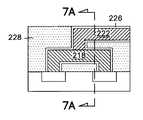
- FIG. 6is a cross-sectional view of the FIG. 5 assembly after forming a diffusion-barrier 226 on conductive structures 218 and 222 ;
- FIG. 7is a cross-sectional view of the FIG. 6 assembly after filling space 224 with one or more insulative materials to form a two-level insulative structure 228 ;
- FIG. 8is a block diagram of an exemplary integrated memory circuit which incorporates the present invention.
- FIGS. 1-8describes and illustrates specific embodiments of the invention. These embodiments, offered not to limit but only to exemplify and teach the concepts of the invention, are shown and described in sufficient detail to enable those skilled in the art to implement or practice the invention. Thus, where appropriate to avoid obscuring the invention, the description may omit certain information known to those of skill in the art.
- FIGS. 1-7show a number of cross-sectional views of a partial integrated-circuits assembly 100 , which taken collectively and sequentially, illustrate a unique exemplary method of making integrated circuits, and more particularly making integrated-circuit wiring in accord with teachings of the present invention.
- the methodbegins with a known integrated-circuit assembly or structure 100 , which can exist within any integrated circuit, a dynamic-random-access memory, for example.
- Assembly 100includes a substrate 212 .
- substrateencompasses a semiconductor wafer as well as structures having one or more insulative, conductive, or semiconductive layers and materials. Thus, for example, the term embraces silicon-on-insulator, silicon-on-sapphire, and other advanced structures.
- Substrate 212supports a number of integrated elements 214 , for example transistors 214 a and 214 b .
- Transistors 214 a and 214 bare covered by a mask layer 216 , which, for example, comprises photoresist.
- the transistorsare metal-oxide-semiconductor field-effect transistors (MOSFETs); however, in other embodiments, the transistors are other types of field-effect transistors or bipolar junction transistors, or mixed transistor types. Still other embodiments use other types of integrated devices.
- Layer 216includes two exemplary via holes 216 a and 216 b positioned over respective contact regions (not shown) of transistors 214 a and 214 b and a trench 216 c connecting the via holes.
- the exemplary embodimentforms layer 216 from photoresist, through use of spincoating, lithography, and photoresist remover. Some embodiments use plasma ashing to pattern the photoresist.
- via holes 216 a and 216 bare cylindrical with diameters of about 1000 nanometers and depths of about 500 nanometers.
- Trench 216 cis less than 0.50 microns wide and at least one micron deep. The invention, however, is not limited to any particular mask material, formation technique, geometry, or dimensions.
- FIG. 2shows that the exemplary method next forms a conductive structure 218 on mask 216 , with one or more portions of the conductive structure contacting one or more exposed portions of the transistors.
- thisentails depositing a 20-30-nanometer-thick copper-, silver-, or gold-based seed layer (not shown separately) using a chemical-vapor-deposition, ionized-magnetron sputtering technique, or DC magnetron self-sputtering technique, and then electroplating additional copper-, silver-, or gold-based material on the seed layer to a total thickness of, for example, 0.5 microns.
- a copper-, silver-, or gold-based materialincludes at least 25 weight-percent of the base material.
- An exemplary chemical-vapor-deposition techniquefollows a procedure such as that described in Y. Senzaki, “Chemical Vapor Deposition of Copper Using a New Liquid Precursor with Improved Thermal Stability,” MRS Conference Proceedings of Advanced Metallization and Interconnect Systems for ULSI Applications in 1997, ULSI XIII, P. 451-455, 1998, which is incorporated herein by reference. This procedure yields copper films at a typical deposition rate of 150-170 nanometers per minute at wafer temperatures of 195-225° C. The resistance of these films is in the range of 2.0 micro-ohm-centimeter after annealing at 400° C. for five minutes.
- Exemplary ionized sputtering technique and d-c magnetron sputtering techniquesfollow procedures similar to those outlined in S. M. Rossnagel et al., Metal Ion Deposition from Ionized Magnetron Sputtering Discharge,” J. Vac. Sci. Technology B, 12(1), p. 449-453, 1994. And Z. J. Radzimski et al, “Directional Copper Deposition using D-C Magnetron Self-sputtering,” J. Vac. Sci Technology B 16(3), p. 1102-1106, 1998.
- Exemplary conditions for the ionized-magnetron sputtering operationare: target power range of 10-30 kilowatts for a 200-300 millimeter diameter wafer (or integrated-circuit assembly), RF coil power at 3-5 kilowatts, negative DC bias of 100-200 volts, sputtering argon gas pressurized at 1-35 millitorrs.
- Ionized-magnetron sputteringwhich provides greater acceleration of the metal deposition material than conventional sputtering, forces the sputtered material to more closely conform to the interior profiles of holes and trenches of the targeted surface.
- the exemplary embodimentomits formation of an adhesion layer to promote adhesion of copper (or other materials) to the mask layer.
- Some embodimentsuse a 20-50 nanometer-thick layer of titanium nitride (TiN) over the transistor contacts as an adhesion layer and a diffusion barrier.
- TiNtitanium nitride
- other embodimentsprovide an adhesion layer of titanium nitride.
- the exemplary methodremoves excess material, for example, using a chemical-mechanical planarization or polishing procedure.
- the exemplary methodforms a mask layer 220 over conductive structure 218 .
- Mask layer 220includes an opening (via) 220 a which exposes a portion of conductive structure 218 and a trench 220 b which intersects opening 220 a .
- Exemplary formation of conductive structurefollows a procedure similar to that used to form mask layer 216 and occurs with at least a portion of mask layer 216 still in place.
- FIG. 4shows that the exemplary method next forms a conductive structure 222 on mask 216 , with portions of structure 222 contacting exposed portions of conductive structure 218 .
- thisentails depositing a 20-30-nanometer-thick copper-, silver-, or gold-based seed layer and electroplating additional copper-, silver-, or gold-based material to an exemplary thickness of 0.5 microns. Excess material is then removed using a chemical-mechanical planarization or polishing procedure. Subsequently, one or more higher-level conductive structures can be formed similarly.
- FIG. 5shows that after forming conductive structure 222 , the method removes at least a portion of mask structures 216 and 220 , defining one or more spaces or voids 224 around conductive structures 218 and 222 . Without the surrounding masks, conductive structures 218 and 222 appears as a two-level airbridge.
- the exemplary embodimentremoves substantially all of the mask structures by ashing them in an oxygen plasma.
- the exemplary methodforms a diffusion barrier 226 on at least portions of conductive structures 218 and 222 .
- thisentails growing or depositing a two-to-six nanometer-thick layer of WSiN over substantially all of conductive structures 218 and 222 .
- Exemplary formation of this layer of WSiNoccurs within a hybrid reaction chamber such as that described in co-filed and co-assigned patent application entitled Methods and Apparatus for Making Copper Wiring in Integrated Circuits. This application, attorney docket 303.618US1 (99-0469), is incorporated herein by reference.
- exemplary formation of diffusion barrier 226entails forming a graded composition of tungsten silicide (WSi x ), with x varying from 2.0 to 2.5. This entails heating the assembly to a temperature of 360° C. and introducing hydrogen, tungsten hexafluoride, and silane gases into a process chamber enclosing the assembly.
- the exemplary embodimentintroduces the hydrogen and tungsten hexaflouride gases about one-to-three seconds before introducing the silane gas and stops introducing the silane gas about one-to-three seconds before stopping introduction of the hydrogen and tungsten hexaflouride.
- Exemplary flow rates for the silane and tungsten hexaflouride gasesare respectively 1000 sccm and 14 sccm. These flow rates result in a composition of WSi 2.3 , with a growth rate of approximately 50 nanometers per minute.
- the exemplary methodnitrides the graded composition of WSi x , forming WSi x N y .
- the exemplary nitridationfollows an electron-cyclotron-resonance (ECR) plasma nitridation procedure.
- ECRelectron-cyclotron-resonance
- One version of this procedureis described in A. Hirata et al., WSiN Diffusion Barrier Formed by ECR Plasma Nitridation for Copper Damascene Interconnection, Extended Abstracts of 1998 International Conference on Solid State Devices and Materials, p. 260-261, which is incorporated herein by reference. This entails introducing nitrogen gas and argon gas into the chamber, with the argon gas exciting a plasma.
- the WSi x N yis not a compound-forming barrier, but a stuffed barrier, which prevents diffusion by stuffing nitrogen atoms into diffusion paths, such as interstitial sites, within the tungsten silicide.
- Other embodimentsuses diffusion barriers having different compositions and thicknesses, and some entirely omit a diffusion barrier.
- FIG. 7shows that after completion of diffusion barrier 226 , the exemplary method fills at least a portion of the remainder of space 224 (denoted 224 ′ in FIG. 6 ) with one or more insulative materials to form a two-level insulative structure 228 .
- the exemplary embodimentfills substantially all of space 224 , which was previously occupied by mask structures 216 and 220 , with a single dielectric material using a single procedure. More particularly, the exemplary embodiment vapor deposits a silicon oxide, such as SiO 2 , or low-k (that is, low-dielectric-constant) materials, such as xerogels or aerogels.
- Various methodssuch as physical-vapor deposition, chemical-vapor deposition, spin-coating, sol-gel procedures, and so forth can be used to apply these dielectrics.
- FIG. 8shows one example of the unlimited number of applications for one or more embodiments of the present invention: a generic integrated memory circuit 600 .
- Circuit 600which operates according to well-known and understood principles, is generally coupled to a processor (not shown) to form a computer system. More precisely, circuit 600 includes a memory array 642 which comprises a number of memory cells 643 a - 643 d , a column address decoder 644 , and a row address decoder 645 , bit lines 646 , word lines 647 , and voltage-sense-amplifier circuit 648 coupled to bit lines 646 .
- each of the memory cells, the address decoders, and the amplifier circuitincludes one or more copper-, silver, or gold-based conductors according to the present invention.
- Other embodimentsuse conductors of other materials, made in accord with one or more methods of the present invention.
- connections between the address decoders, the memory array, the amplifier circuitare implemented using similar interconnects.
- the inventorshave one or more exemplary methods for making integrated-circuit wiring from materials, such as copper-, silver-, and gold-based metals, some of which allow fabrication of wiring with fewer steps and lower electrical resistance than some conventional methods.
- One exemplary methodinitially forms a first mask and a first metal structure on the first mask and then forms a second mask and a second metal structure on the second mask, with the first mask and first metal structure still in place.
- this exemplary methodremoves both masks in a single removal procedure, forms a diffusion barrier to both metal structures in a single formation procedure, and fills insulative material in and around both metal structures in a single fill procedure.
- Applying one or more procedures across multiple wiring levels, as in this embodimentultimately precludes the necessity of applying these procedures separately to each wiring level and thus promises to simplify fabrication.
Landscapes
- Engineering & Computer Science (AREA)
- Physics & Mathematics (AREA)
- Condensed Matter Physics & Semiconductors (AREA)
- General Physics & Mathematics (AREA)
- Manufacturing & Machinery (AREA)
- Computer Hardware Design (AREA)
- Microelectronics & Electronic Packaging (AREA)
- Power Engineering (AREA)
- Plasma & Fusion (AREA)
- Internal Circuitry In Semiconductor Integrated Circuit Devices (AREA)
Abstract
Description
Claims (25)
Priority Applications (1)
| Application Number | Priority Date | Filing Date | Title |
|---|---|---|---|
| US11/458,975US7368378B2 (en) | 2000-01-18 | 2006-07-20 | Methods for making integrated-circuit wiring from copper, silver, gold, and other metals |
Applications Claiming Priority (2)
| Application Number | Priority Date | Filing Date | Title |
|---|---|---|---|
| US09/484,303US7262130B1 (en) | 2000-01-18 | 2000-01-18 | Methods for making integrated-circuit wiring from copper, silver, gold, and other metals |
| US11/458,975US7368378B2 (en) | 2000-01-18 | 2006-07-20 | Methods for making integrated-circuit wiring from copper, silver, gold, and other metals |
Related Parent Applications (1)
| Application Number | Title | Priority Date | Filing Date |
|---|---|---|---|
| US09/484,303ContinuationUS7262130B1 (en) | 2000-01-18 | 2000-01-18 | Methods for making integrated-circuit wiring from copper, silver, gold, and other metals |
Publications (2)
| Publication Number | Publication Date |
|---|---|
| US20060292857A1 US20060292857A1 (en) | 2006-12-28 |
| US7368378B2true US7368378B2 (en) | 2008-05-06 |
Family
ID=34102658
Family Applications (5)
| Application Number | Title | Priority Date | Filing Date |
|---|---|---|---|
| US09/484,303Expired - LifetimeUS7262130B1 (en) | 2000-01-18 | 2000-01-18 | Methods for making integrated-circuit wiring from copper, silver, gold, and other metals |
| US10/931,541Expired - LifetimeUS7253521B2 (en) | 2000-01-18 | 2004-08-31 | Methods for making integrated-circuit wiring from copper, silver, gold, and other metals |
| US11/457,099Expired - Fee RelatedUS7402516B2 (en) | 2000-01-18 | 2006-07-12 | Method for making integrated circuits |
| US11/458,975Expired - Fee RelatedUS7368378B2 (en) | 2000-01-18 | 2006-07-20 | Methods for making integrated-circuit wiring from copper, silver, gold, and other metals |
| US11/652,310AbandonedUS20070141830A1 (en) | 2000-01-18 | 2007-01-11 | Methods for making integrated-circuit wiring from copper, silver, gold, and other metals |
Family Applications Before (3)
| Application Number | Title | Priority Date | Filing Date |
|---|---|---|---|
| US09/484,303Expired - LifetimeUS7262130B1 (en) | 2000-01-18 | 2000-01-18 | Methods for making integrated-circuit wiring from copper, silver, gold, and other metals |
| US10/931,541Expired - LifetimeUS7253521B2 (en) | 2000-01-18 | 2004-08-31 | Methods for making integrated-circuit wiring from copper, silver, gold, and other metals |
| US11/457,099Expired - Fee RelatedUS7402516B2 (en) | 2000-01-18 | 2006-07-12 | Method for making integrated circuits |
Family Applications After (1)
| Application Number | Title | Priority Date | Filing Date |
|---|---|---|---|
| US11/652,310AbandonedUS20070141830A1 (en) | 2000-01-18 | 2007-01-11 | Methods for making integrated-circuit wiring from copper, silver, gold, and other metals |
Country Status (1)
| Country | Link |
|---|---|
| US (5) | US7262130B1 (en) |
Cited By (4)
| Publication number | Priority date | Publication date | Assignee | Title |
|---|---|---|---|---|
| US20070111365A1 (en)* | 2005-11-11 | 2007-05-17 | Semiconductor Energy Laboratory Co., Ltd. | Manufacturing method of microstructure and microelectromechanical system |
| US7535103B2 (en) | 2000-01-18 | 2009-05-19 | Micron Technology, Inc. | Structures and methods to enhance copper metallization |
| US8525339B2 (en) | 2011-07-27 | 2013-09-03 | International Business Machines Corporation | Hybrid copper interconnect structure and method of fabricating same |
| US9312203B2 (en) | 2013-01-02 | 2016-04-12 | Globalfoundries Inc. | Dual damascene structure with liner |
Families Citing this family (26)
| Publication number | Priority date | Publication date | Assignee | Title |
|---|---|---|---|---|
| US6429120B1 (en)* | 2000-01-18 | 2002-08-06 | Micron Technology, Inc. | Methods and apparatus for making integrated-circuit wiring from copper, silver, gold, and other metals |
| US7211512B1 (en)* | 2000-01-18 | 2007-05-01 | Micron Technology, Inc. | Selective electroless-plated copper metallization |
| US7262130B1 (en)* | 2000-01-18 | 2007-08-28 | Micron Technology, Inc. | Methods for making integrated-circuit wiring from copper, silver, gold, and other metals |
| US6376370B1 (en)* | 2000-01-18 | 2002-04-23 | Micron Technology, Inc. | Process for providing seed layers for using aluminum, copper, gold and silver metallurgy process for providing seed layers for using aluminum, copper, gold and silver metallurgy |
| US6674167B1 (en) | 2000-05-31 | 2004-01-06 | Micron Technology, Inc. | Multilevel copper interconnect with double passivation |
| US6921551B2 (en) | 2000-08-10 | 2005-07-26 | Asm Nutool, Inc. | Plating method and apparatus for controlling deposition on predetermined portions of a workpiece |
| US6511912B1 (en)* | 2000-08-22 | 2003-01-28 | Micron Technology, Inc. | Method of forming a non-conformal layer over and exposing a trench |
| US7687917B2 (en)* | 2002-05-08 | 2010-03-30 | Nec Electronics Corporation | Single damascene structure semiconductor device having silicon-diffused metal wiring layer |
| JP4316469B2 (en)* | 2004-10-15 | 2009-08-19 | 株式会社東芝 | Automatic design equipment |
| US7361585B2 (en)* | 2004-12-23 | 2008-04-22 | Advantech Global, Ltd | System for and method of planarizing the contact region of a via by use of a continuous inline vacuum deposition |
| CN101432251A (en)* | 2006-04-27 | 2009-05-13 | 佳能株式会社 | 4-arylfluorene compound and organic light-emitting device using same |
| US8500985B2 (en)* | 2006-07-21 | 2013-08-06 | Novellus Systems, Inc. | Photoresist-free metal deposition |
| KR100760920B1 (en)* | 2006-07-25 | 2007-09-21 | 동부일렉트로닉스 주식회사 | How to Form Copper Wiring in Semiconductor Integrated Circuit Devices |
| US20080272408A1 (en)* | 2007-05-01 | 2008-11-06 | Dsm Solutions, Inc. | Active area junction isolation structure and junction isolated transistors including igfet, jfet and mos transistors and method for making |
| TWI514608B (en)* | 2010-01-14 | 2015-12-21 | Dow Global Technologies Llc | Moisture-proof photovoltaic device with exposed conductive grid |
| US9059349B2 (en)* | 2010-02-09 | 2015-06-16 | Dow Global Technologies Llc | Moisture resistant photovoltaic devices with improved adhesion of barrier film |
| US8957519B2 (en)* | 2010-10-22 | 2015-02-17 | International Business Machines Corporation | Structure and metallization process for advanced technology nodes |
| JP2012148428A (en)* | 2011-01-17 | 2012-08-09 | Toshiba Tec Corp | Method of manufacturing inkjet head |
| US20140120711A1 (en)* | 2012-10-26 | 2014-05-01 | United Microelectronics Corp. | Method of forming metal gate |
| KR101983137B1 (en)* | 2013-03-04 | 2019-05-28 | 삼성전기주식회사 | Power inductor and manufacturing method thereof |
| KR101998788B1 (en) | 2013-04-22 | 2019-07-11 | 삼성전자주식회사 | Semiconductor Devices and Methods of Fabricating the Same |
| US9564362B2 (en)* | 2015-02-05 | 2017-02-07 | International Business Machines Corporation | Interconnects based on subtractive etching of silver |
| US9286917B1 (en) | 2015-04-30 | 2016-03-15 | Seagate Technology Llc | Write pole formed with evaporation deposition |
| US10615123B2 (en)* | 2018-03-14 | 2020-04-07 | Sandisk Technologies Llc | Three-dimensional memory device containing compositionally graded word line diffusion barrier layer for and methods of forming the same |
| CN109545738A (en)* | 2018-11-12 | 2019-03-29 | 苏州汉骅半导体有限公司 | Air bridges manufacturing method |
| US11094655B2 (en) | 2019-06-13 | 2021-08-17 | Taiwan Semiconductor Manufacturing Co., Ltd. | Semiconductor structure and method for forming the same |
Citations (204)
| Publication number | Priority date | Publication date | Assignee | Title |
|---|---|---|---|---|
| US2842438A (en) | 1956-08-02 | 1958-07-08 | American Metal Climax Inc | Copper-zirconium alloys |
| US3515663A (en) | 1968-02-01 | 1970-06-02 | Hewlett Packard Co | Triode sputtering apparatus using an electron emitter |
| US3954570A (en) | 1974-11-11 | 1976-05-04 | Amp Incorporated | Sensitized polyimides and circuit elements thereof |
| US4213818A (en) | 1979-01-04 | 1980-07-22 | Signetics Corporation | Selective plasma vapor etching process |
| US4386116A (en) | 1981-12-24 | 1983-05-31 | International Business Machines Corporation | Process for making multilayer integrated circuit substrate |
| US4394223A (en) | 1981-10-06 | 1983-07-19 | The United States Of America As Represented By The Secretary Of The Air Force | Tin and gold plating process |
| US4423547A (en) | 1981-06-01 | 1984-01-03 | International Business Machines Corporation | Method for forming dense multilevel interconnection metallurgy for semiconductor devices |
| US4565157A (en) | 1983-03-29 | 1986-01-21 | Genus, Inc. | Method and apparatus for deposition of tungsten silicides |
| US4574095A (en) | 1984-11-19 | 1986-03-04 | International Business Machines Corporation | Selective deposition of copper |
| US4762728A (en) | 1985-04-09 | 1988-08-09 | Fairchild Semiconductor Corporation | Low temperature plasma nitridation process and applications of nitride films formed thereby |
| US4788082A (en) | 1984-02-13 | 1988-11-29 | Schmitt Jerome J | Method and apparatus for the deposition of solid films of a material from a jet stream entraining the gaseous phase of said material |
| US4824544A (en) | 1987-10-29 | 1989-04-25 | International Business Machines Corporation | Large area cathode lift-off sputter deposition device |
| US4847111A (en) | 1988-06-30 | 1989-07-11 | Hughes Aircraft Company | Plasma-nitridated self-aligned tungsten system for VLSI interconnections |
| US4931410A (en) | 1987-08-25 | 1990-06-05 | Hitachi, Ltd. | Process for producing semiconductor integrated circuit device having copper interconnections and/or wirings, and device produced |
| US4933743A (en) | 1989-03-11 | 1990-06-12 | Fairchild Semiconductor Corporation | High performance interconnect system for an integrated circuit |
| US4948459A (en) | 1988-01-20 | 1990-08-14 | U.S. Philips Corporation | Method of enabling electrical connection to a substructure forming part of an electronic device |
| US4962058A (en) | 1989-04-14 | 1990-10-09 | International Business Machines Corporation | Process for fabricating multi-level integrated circuit wiring structure from a single metal deposit |
| US4990229A (en) | 1989-06-13 | 1991-02-05 | Plasma & Materials Technologies, Inc. | High density plasma deposition and etching apparatus |
| US4996584A (en) | 1985-01-31 | 1991-02-26 | Gould, Inc. | Thin-film electrical connections for integrated circuits |
| US5000818A (en) | 1989-08-14 | 1991-03-19 | Fairchild Semiconductor Corporation | Method of fabricating a high performance interconnect system for an integrated circuit |
| US5019531A (en) | 1988-05-23 | 1991-05-28 | Nippon Telegraph And Telephone Corporation | Process for selectively growing thin metallic film of copper or gold |
| US5034799A (en) | 1989-02-22 | 1991-07-23 | Kabushiki Kaisha Toshiba | Semiconductor integrated circuit device having a hollow multi-layered lead structure |
| US5071518A (en) | 1989-10-24 | 1991-12-10 | Microelectronics And Computer Technology Corporation | Method of making an electrical multilayer interconnect |
| US5084412A (en) | 1989-10-02 | 1992-01-28 | Kabushiki Kaisha Toshiba | Method of manufacturing a semiconductor device with a copper wiring layer |
| US5100499A (en) | 1989-12-20 | 1992-03-31 | Texas Instruments Incorporated | Copper dry etch process using organic and amine radicals |
| US5130274A (en) | 1991-04-05 | 1992-07-14 | International Business Machines Corporation | Copper alloy metallurgies for VLSI interconnection structures |
| US5158986A (en) | 1991-04-05 | 1992-10-27 | Massachusetts Institute Of Technology | Microcellular thermoplastic foamed with supercritical fluid |
| US5171713A (en) | 1990-01-10 | 1992-12-15 | Micrunity Systems Eng | Process for forming planarized, air-bridge interconnects on a semiconductor substrate |
| US5173442A (en) | 1990-07-23 | 1992-12-22 | Microelectronics And Computer Technology Corporation | Methods of forming channels and vias in insulating layers |
| US5231056A (en) | 1992-01-15 | 1993-07-27 | Micron Technology, Inc. | Tungsten silicide (WSix) deposition process for semiconductor manufacture |
| US5240878A (en) | 1991-04-26 | 1993-08-31 | International Business Machines Corporation | Method for forming patterned films on a substrate |
| US5243222A (en) | 1991-04-05 | 1993-09-07 | International Business Machines Corporation | Copper alloy metallurgies for VLSI interconnection structures |
| JPH05267643A (en) | 1992-03-19 | 1993-10-15 | Fujitsu Ltd | Semiconductor device and manufacturing method thereof |
| US5256205A (en) | 1990-05-09 | 1993-10-26 | Jet Process Corporation | Microwave plasma assisted supersonic gas jet deposition of thin film materials |
| JPH05295533A (en) | 1992-04-17 | 1993-11-09 | Sony Corp | Film forming method and film forming device using electron cyclotron resonance |
| US5348811A (en) | 1986-07-25 | 1994-09-20 | Fuji Photo Film Co., Ltd. | Recording medium and method of performing recording/producing on the recording medium |
| US5354712A (en) | 1992-11-12 | 1994-10-11 | Northern Telecom Limited | Method for forming interconnect structures for integrated circuits |
| US5371042A (en) | 1992-06-16 | 1994-12-06 | Applied Materials, Inc. | Method of filling contacts in semiconductor devices |
| US5374849A (en) | 1992-03-02 | 1994-12-20 | Mitsubishi Denki Kabushiki Kaisha | Conductive layer connection structure of semiconductor device |
| US5384284A (en) | 1993-10-01 | 1995-01-24 | Micron Semiconductor, Inc. | Method to form a low resistant bond pad interconnect |
| US5401680A (en) | 1992-02-18 | 1995-03-28 | National Semiconductor Corporation | Method for forming a ceramic oxide capacitor having barrier layers |
| US5413962A (en) | 1994-07-15 | 1995-05-09 | United Microelectronics Corporation | Multi-level conductor process in VLSI fabrication utilizing an air bridge |
| US5413687A (en) | 1991-11-27 | 1995-05-09 | Rogers Corporation | Method for metallizing fluoropolymer substrates |
| US5426330A (en) | 1992-02-26 | 1995-06-20 | International Business Machines Corporation | Refractory metal capped low resistivity metal conductor lines and vias |
| US5442237A (en) | 1991-10-21 | 1995-08-15 | Motorola Inc. | Semiconductor device having a low permittivity dielectric |
| US5447887A (en) | 1994-04-01 | 1995-09-05 | Motorola, Inc. | Method for capping copper in semiconductor devices |
| US5451804A (en) | 1994-05-11 | 1995-09-19 | United Microelectronics Corporation | VLSI device with global planarization |
| US5470801A (en) | 1993-06-28 | 1995-11-28 | Lsi Logic Corporation | Low dielectric constant insulation layer for integrated circuit structure and method of making same |
| US5470789A (en) | 1993-03-19 | 1995-11-28 | Fujitsu Limited | Process for fabricating integrated circuit devices |
| JPH07321111A (en) | 1994-05-26 | 1995-12-08 | Meidensha Corp | Method of forming electroless plated interconnection for integrated circuit |
| US5495667A (en) | 1994-11-07 | 1996-03-05 | Micron Technology, Inc. | Method for forming contact pins for semiconductor dice and interconnects |
| US5506449A (en) | 1993-03-24 | 1996-04-09 | Kawasaki Steel Corporation | Interconnection structure for semiconductor integrated circuit and manufacture of the same |
| US5539060A (en) | 1993-07-30 | 1996-07-23 | Nippon Zeon Co., Ltd. | Method for hydrogenation of metathesis polymers |
| US5538922A (en) | 1991-06-03 | 1996-07-23 | Motorola, Inc. | Method for forming contact to a semiconductor device |
| US5595937A (en) | 1995-04-13 | 1997-01-21 | Nec Corporation | Method for fabricating semiconductor device with interconnections buried in trenches |
| US5609721A (en) | 1994-03-11 | 1997-03-11 | Fujitsu Limited | Semiconductor device manufacturing apparatus and its cleaning method |
| US5625233A (en) | 1995-01-13 | 1997-04-29 | Ibm Corporation | Thin film multi-layer oxygen diffusion barrier consisting of refractory metal, refractory metal aluminide, and aluminum oxide |
| US5633200A (en) | 1996-05-24 | 1997-05-27 | Micron Technology, Inc. | Process for manufacturing a large grain tungsten nitride film and process for manufacturing a lightly nitrided titanium salicide diffusion barrier with a large grain tungsten nitride cover layer |
| US5635253A (en) | 1994-08-30 | 1997-06-03 | International Business Machines Corporation | Method of replenishing electroless gold plating baths |
| US5654245A (en) | 1993-03-23 | 1997-08-05 | Sharp Microelectronics Technology, Inc. | Implantation of nucleating species for selective metallization and products thereof |
| US5670420A (en) | 1994-12-05 | 1997-09-23 | Hyundai Electronics Industries Co., Ltd. | Method of forming metal interconnection layer of semiconductor device |
| US5674787A (en) | 1996-01-16 | 1997-10-07 | Sematech, Inc. | Selective electroless copper deposited interconnect plugs for ULSI applications |
| US5679608A (en) | 1994-12-21 | 1997-10-21 | Advanced Micro Devices, Inc. | Processing techniques for achieving production-worthy, low dielectric, low dielectric, low interconnect resistance and high performance IC |
| US5681441A (en) | 1992-12-22 | 1997-10-28 | Elf Technologies, Inc. | Method for electroplating a substrate containing an electroplateable pattern |
| EP0808915A2 (en) | 1996-05-23 | 1997-11-26 | Applied Materials, Inc. | Chemical vapor deposition and sputtering method and apparatus |
| US5693563A (en) | 1996-07-15 | 1997-12-02 | Chartered Semiconductor Manufacturing Pte Ltd. | Etch stop for copper damascene process |
| US5695810A (en) | 1996-11-20 | 1997-12-09 | Cornell Research Foundation, Inc. | Use of cobalt tungsten phosphide as a barrier material for copper metallization |
| US5719447A (en) | 1993-06-03 | 1998-02-17 | Intel Corporation | Metal alloy interconnections for integrated circuits |
| US5719089A (en) | 1996-06-21 | 1998-02-17 | Vanguard International Semiconductor Corporation | Method for etching polymer-assisted reduced small contacts for ultra large scale integration semiconductor devices |
| US5719410A (en) | 1993-12-28 | 1998-02-17 | Kabushiki Kaisha Toshiba | Semiconductor device wiring or electrode |
| US5739579A (en) | 1992-06-29 | 1998-04-14 | Intel Corporation | Method for forming interconnections for semiconductor fabrication and semiconductor device having such interconnections |
| US5763953A (en) | 1993-01-05 | 1998-06-09 | Kabushiki Kaisha Toshiba | Semiconductor device and method of manufacturing the same |
| US5780358A (en) | 1996-04-08 | 1998-07-14 | Chartered Semiconductor Manufacturing Ltd. | Method for chemical-mechanical polish (CMP) planarizing of cooper containing conductor layers |
| US5785570A (en) | 1994-07-26 | 1998-07-28 | Pixtech S.A. | Anode for a flat display screen |
| US5789264A (en) | 1996-03-27 | 1998-08-04 | Daewoo Electronics Co., Ltd. | Method for manufacturing a thin film actuated mirror having a flat light reflecting surface |
| US5792522A (en) | 1996-09-18 | 1998-08-11 | Intel Corporation | High density plasma physical vapor deposition |
| US5801098A (en) | 1996-09-03 | 1998-09-01 | Motorola, Inc. | Method of decreasing resistivity in an electrically conductive layer |
| US5814557A (en) | 1996-05-20 | 1998-09-29 | Motorola, Inc. | Method of forming an interconnect structure |
| US5821168A (en) | 1997-07-16 | 1998-10-13 | Motorola, Inc. | Process for forming a semiconductor device |
| US5824599A (en) | 1996-01-16 | 1998-10-20 | Cornell Research Foundation, Inc. | Protected encapsulation of catalytic layer for electroless copper interconnect |
| US5840625A (en) | 1995-03-30 | 1998-11-24 | Siemens Aktiengesellschaft | Method of fabricating integrated circuit interconnection employing tungsten/aluminum layers |
| US5858877A (en) | 1992-07-28 | 1999-01-12 | Micron Technology, Inc. | Self-aligned process for making contacts to silicon substrates during the manufacture of integrated circuits therein |
| US5889295A (en) | 1996-02-26 | 1999-03-30 | Kabushiki Kaisha Toshiba | Semiconductor device |
| US5891797A (en) | 1997-10-20 | 1999-04-06 | Micron Technology, Inc. | Method of forming a support structure for air bridge wiring of an integrated circuit |
| US5891804A (en) | 1996-04-18 | 1999-04-06 | Texas Instruments Incorporated | Process for conductors with selective deposition |
| US5895740A (en) | 1996-11-13 | 1999-04-20 | Vanguard International Semiconductor Corp. | Method of forming contact holes of reduced dimensions by using in-situ formed polymeric sidewall spacers |
| US5897370A (en) | 1994-08-05 | 1999-04-27 | International Business Machines Corporation | High aspect ratio low resistivity lines/vias by surface diffusion |
| US5899740A (en) | 1997-03-04 | 1999-05-04 | Samsung Electronics Co., Ltd. | Methods of fabricating copper interconnects for integrated circuits |
| US5907772A (en) | 1996-02-26 | 1999-05-25 | Nec Corporation | Method of producing cylindrical storage node of stacked capacitor in memory cell |
| US5911113A (en) | 1997-03-18 | 1999-06-08 | Applied Materials, Inc. | Silicon-doped titanium wetting layer for aluminum plug |
| US5925930A (en) | 1996-05-21 | 1999-07-20 | Micron Technology, Inc. | IC contacts with palladium layer and flexible conductive epoxy bumps |
| US5930669A (en) | 1997-04-03 | 1999-07-27 | International Business Machines Corporation | Continuous highly conductive metal wiring structures and method for fabricating the same |
| US5932928A (en) | 1997-07-03 | 1999-08-03 | Micron Technology, Inc. | Semiconductor circuit interconnections and methods of making such interconnections |
| US5937320A (en) | 1998-04-08 | 1999-08-10 | International Business Machines Corporation | Barrier layers for electroplated SnPb eutectic solder joints |
| US5939771A (en) | 1995-10-30 | 1999-08-17 | Nec Corporation | Semiconductor device having an organic resin layer and silicon oxide layer containing fluorine for preventing crosstalk between metal lines and a method of manufacturing the same |
| US5940733A (en) | 1995-05-03 | 1999-08-17 | Applied Materials, Inc. | Method of making polysilicon/tungsten silicide multilayer composite on an integrated circuit structure |
| US5948467A (en) | 1998-07-24 | 1999-09-07 | Sharp Laboratories Of America, Inc. | Enhanced CVD copper adhesion by two-step deposition process |
| US5962923A (en) | 1995-08-07 | 1999-10-05 | Applied Materials, Inc. | Semiconductor device having a low thermal budget metal filling and planarization of contacts, vias and trenches |
| US5969398A (en) | 1997-08-07 | 1999-10-19 | Mitsubishi Denki Kabushiki Kaisha | Method for producing a semiconductor device and a semiconductor device |
| US5968327A (en) | 1997-04-14 | 1999-10-19 | Anelva Corporation | Ionizing sputter device using a coil shield |
| US5972179A (en) | 1997-09-30 | 1999-10-26 | Lucent Technologies Inc. | Silicon IC contacts using composite TiN barrier layer |
| US5972804A (en) | 1997-08-05 | 1999-10-26 | Motorola, Inc. | Process for forming a semiconductor device |
| US5976710A (en) | 1991-08-05 | 1999-11-02 | International Business Machines Corporation | Low TCE polyimides as improved insulator in multilayer interconnect structures |
| US5981350A (en) | 1998-05-29 | 1999-11-09 | Micron Technology, Inc. | Method for forming high capacitance memory cells |
| US5985759A (en) | 1998-02-24 | 1999-11-16 | Applied Materials, Inc. | Oxygen enhancement of ion metal plasma (IMP) sputter deposited barrier layers |
| US5989623A (en) | 1997-08-19 | 1999-11-23 | Applied Materials, Inc. | Dual damascene metallization |
| US6002175A (en) | 1995-10-05 | 1999-12-14 | Mitsubishi Denki Kabushiki Kaisha | Semiconductor device with improved connection hole for embedding an electrically conductive layer portion |
| US6001736A (en) | 1995-03-02 | 1999-12-14 | Kawasaki Steel Corporation | Method of manufacturing semiconductor device and an apparatus for manufacturing the same |
| US6004884A (en) | 1996-02-15 | 1999-12-21 | Lam Research Corporation | Methods and apparatus for etching semiconductor wafers |
| US6008117A (en) | 1996-03-29 | 1999-12-28 | Texas Instruments Incorporated | Method of forming diffusion barriers encapsulating copper |
| US6015465A (en) | 1998-04-08 | 2000-01-18 | Applied Materials, Inc. | Temperature control system for semiconductor process chamber |
| US6016000A (en) | 1998-04-22 | 2000-01-18 | Cvc, Inc. | Ultra high-speed chip semiconductor integrated circuit interconnect structure and fabrication method using free-space dielectrics |
| US6017820A (en) | 1998-07-17 | 2000-01-25 | Cutek Research, Inc. | Integrated vacuum and plating cluster system |
| EP0304046B1 (en) | 1987-08-19 | 2000-01-26 | Fujitsu Limited | A method of stripping a resist mask |
| US6020243A (en) | 1997-07-24 | 2000-02-01 | Texas Instruments Incorporated | Zirconium and/or hafnium silicon-oxynitride gate dielectric |
| US6022802A (en) | 1999-03-18 | 2000-02-08 | Taiwan Semiconductor Manufacturing Company | Low dielectric constant intermetal dielectric (IMD) by formation of air gap between metal lines |
| US6028362A (en) | 1997-05-12 | 2000-02-22 | Yamaha Corporation | Damascene wiring with flat surface |
| US6030895A (en) | 1995-01-03 | 2000-02-29 | International Business Machines Corporation | Method of making a soft metal conductor |
| US6030877A (en) | 1997-10-06 | 2000-02-29 | Industrial Technology Research Institute | Electroless gold plating method for forming inductor structures |
| US6037248A (en) | 1997-06-13 | 2000-03-14 | Micron Technology, Inc. | Method of fabricating integrated circuit wiring with low RC time delay |
| US6051858A (en) | 1996-07-26 | 2000-04-18 | Symetrix Corporation | Ferroelectric/high dielectric constant integrated circuit and method of fabricating same |
| US6065424A (en) | 1995-12-19 | 2000-05-23 | Cornell Research Foundation, Inc. | Electroless deposition of metal films with spray processor |
| US6069068A (en) | 1997-05-30 | 2000-05-30 | International Business Machines Corporation | Sub-quarter-micron copper interconnections with improved electromigration resistance and reduced defect sensitivity |
| US6071810A (en) | 1996-12-24 | 2000-06-06 | Kabushiki Kaisha Toshiba | Method of filling contact holes and wiring grooves of a semiconductor device |
| US6090697A (en) | 1997-06-30 | 2000-07-18 | Texas Instruments Incorporated | Etchstop for integrated circuits |
| US6091136A (en) | 1997-06-19 | 2000-07-18 | Micron Technology, Inc. | Plastic lead frames for semiconductor devices |
| US6103320A (en) | 1998-03-05 | 2000-08-15 | Shincron Co., Ltd. | Method for forming a thin film of a metal compound by vacuum deposition |
| US6120641A (en) | 1998-05-12 | 2000-09-19 | Semitool, Inc. | Process architecture and manufacturing tool sets employing hard mask patterning for use in the manufacture of one or more metallization levels on a workpiece |
| US6121150A (en) | 1999-04-22 | 2000-09-19 | Advanced Micro Devices, Inc. | Sputter-resistant hardmask for damascene trench/via formation |
| US6126989A (en) | 1997-08-22 | 2000-10-03 | Micron Technology, Inc. | Copper electroless deposition on a titanium-containing surface |
| US6140234A (en) | 1998-01-20 | 2000-10-31 | International Business Machines Corporation | Method to selectively fill recesses with conductive metal |
| US6139699A (en) | 1997-05-27 | 2000-10-31 | Applied Materials, Inc. | Sputtering methods for depositing stress tunable tantalum and tantalum nitride films |
| US6140228A (en) | 1997-11-13 | 2000-10-31 | Cypress Semiconductor Corporation | Low temperature metallization process |
| US6143655A (en) | 1998-02-25 | 2000-11-07 | Micron Technology, Inc. | Methods and structures for silver interconnections in integrated circuits |
| US6143641A (en) | 2000-01-26 | 2000-11-07 | National Semiconductor Corporation | Structure and method for controlling copper diffusion and for utilizing low K materials for copper interconnects in integrated circuit structures |
| US6143671A (en) | 1997-11-21 | 2000-11-07 | Nec Corporation | Semiconductor device manufacturing method |
| US6143646A (en) | 1997-06-03 | 2000-11-07 | Motorola Inc. | Dual in-laid integrated circuit structure with selectively positioned low-K dielectric isolation and method of formation |
| US6150214A (en) | 1997-11-21 | 2000-11-21 | Texas Instruments Incorporated | Titanium nitride metal interconnection system and method of forming the same |
| US6150261A (en) | 1999-05-25 | 2000-11-21 | United Microelectronics Corp. | Method of fabricating semiconductor device for preventing antenna effect |
| US6153507A (en) | 1997-01-13 | 2000-11-28 | Nec Corporation | Method of fabricating semiconductor device providing effective resistance against metal layer oxidation and diffusion |
| US6162583A (en) | 1998-03-20 | 2000-12-19 | Industrial Technology Research Institute | Method for making intermetal dielectrics (IMD) on semiconductor integrated circuits using low dielectric constant spin-on polymers |
| US6169024B1 (en) | 1998-09-30 | 2001-01-02 | Intel Corporation | Process to manufacture continuous metal interconnects |
| US6171661B1 (en) | 1998-02-25 | 2001-01-09 | Applied Materials, Inc. | Deposition of copper with increased adhesion |
| US6174804B1 (en) | 1998-05-26 | 2001-01-16 | United Microelectronics Corp. | Dual damascene manufacturing process |
| US6177350B1 (en) | 1998-04-14 | 2001-01-23 | Applied Materials, Inc. | Method for forming a multilayered aluminum-comprising structure on a substrate |
| US6181012B1 (en) | 1998-04-27 | 2001-01-30 | International Business Machines Corporation | Copper interconnection structure incorporating a metal seed layer |
| US6183564B1 (en) | 1998-11-12 | 2001-02-06 | Tokyo Electron Limited | Buffer chamber for integrating physical and chemical vapor deposition chambers together in a processing system |
| US6187656B1 (en) | 1997-10-07 | 2001-02-13 | Texas Instruments Incorporated | CVD-based process for manufacturing stable low-resistivity poly-metal gate electrodes |
| US6190732B1 (en) | 1998-09-03 | 2001-02-20 | Cvc Products, Inc. | Method and system for dispensing process gas for fabricating a device on a substrate |
| US6197181B1 (en) | 1998-03-20 | 2001-03-06 | Semitool, Inc. | Apparatus and method for electrolytically depositing a metal on a microelectronic workpiece |
| US6197688B1 (en) | 1998-02-12 | 2001-03-06 | Motorola Inc. | Interconnect structure in a semiconductor device and method of formation |
| US6207558B1 (en) | 1999-10-21 | 2001-03-27 | Applied Materials, Inc. | Barrier applications for aluminum planarization |
| US6208016B1 (en) | 1998-09-10 | 2001-03-27 | Micron Technology, Inc. | Forming submicron integrated-circuit wiring from gold, silver, copper and other metals |
| US6207553B1 (en) | 1999-01-26 | 2001-03-27 | Advanced Micro Devices, Inc. | Method of forming multiple levels of patterned metallization |
| US6211073B1 (en) | 1998-02-27 | 2001-04-03 | Micron Technology, Inc. | Methods for making copper and other metal interconnections in integrated circuits |
| US6215186B1 (en) | 1998-01-12 | 2001-04-10 | Texas Instruments Incorporated | System and method of forming a tungstein plug |
| US6221763B1 (en) | 1999-04-05 | 2001-04-24 | Micron Technology, Inc. | Method of forming a metal seed layer for subsequent plating |
| US6232219B1 (en) | 1998-05-20 | 2001-05-15 | Micron Technology, Inc. | Self-limiting method of reducing contamination in a contact opening, method of making contacts and semiconductor devices therewith, and resulting structures |
| US20010002333A1 (en) | 1999-03-05 | 2001-05-31 | Chao-Yuan Huang | Method of fabricating dual damascene structure |
| US6245662B1 (en) | 1998-07-23 | 2001-06-12 | Applied Materials, Inc. | Method of producing an interconnect structure for an integrated circuit |
| US6249056B1 (en) | 1997-08-16 | 2001-06-19 | Samsung Electronics Co., Ltd. | Low resistance interconnect for a semiconductor device and method of fabricating the same |
| US6251781B1 (en) | 1999-08-16 | 2001-06-26 | Chartered Semiconductor Manufacturing Ltd. | Method to deposit a platinum seed layer for use in selective copper plating |
| US6258707B1 (en) | 1999-01-07 | 2001-07-10 | International Business Machines Corporation | Triple damascence tungsten-copper interconnect structure |
| US6265311B1 (en) | 1999-04-27 | 2001-07-24 | Tokyo Electron Limited | PECVD of TaN films from tantalum halide precursors |
| US6277263B1 (en) | 1998-03-20 | 2001-08-21 | Semitool, Inc. | Apparatus and method for electrolytically depositing copper on a semiconductor workpiece |
| US6284656B1 (en) | 1998-08-04 | 2001-09-04 | Micron Technology, Inc. | Copper metallurgy in integrated circuits |
| US6287954B1 (en) | 1997-05-30 | 2001-09-11 | International Business Machines Corporation | Method of forming copper interconnections with enhanced electromigration resistance and reduced defect sensitivity |
| US6288447B1 (en) | 1999-01-22 | 2001-09-11 | Mitsubishi Denki Kabushiki Kaisha | Semiconductor device including a plurality of interconnection layers |
| US6303498B1 (en) | 1999-08-20 | 2001-10-16 | Taiwan Semiconductor Manufacturing Company | Method for preventing seed layer oxidation for high aspect gap fill |
| US6323553B1 (en) | 1997-02-03 | 2001-11-27 | Texas Instrument Incorporated | Reduced temperature contact/via filling |
| US6333255B1 (en) | 1997-08-21 | 2001-12-25 | Matsushita Electronics Corporation | Method for making semiconductor device containing low carbon film for interconnect structures |
| US6342448B1 (en) | 2000-05-31 | 2002-01-29 | Taiwan Semiconductor Manufacturing Company | Method of fabricating barrier adhesion to low-k dielectric layers in a copper damascene process |
| US20020014646A1 (en) | 1997-01-31 | 2002-02-07 | Robert Tsu | Integrated circuit capacitor |
| US6350678B1 (en) | 1999-09-17 | 2002-02-26 | Advanced Micro Devices, Inc. | Chemical-mechanical polishing of semiconductors |
| US20020028552A1 (en) | 1998-10-17 | 2002-03-07 | Ki-Young Lee | Capacitor of semiconductor integrated circuit and its fabricating method |
| US6358842B1 (en) | 2000-08-07 | 2002-03-19 | Chartered Semiconductor Manufacturing Ltd. | Method to form damascene interconnects with sidewall passivation to protect organic dielectrics |
| US6358849B1 (en) | 1997-12-23 | 2002-03-19 | Texas Instruments Incorporated | Integrated circuit interconnect and method |
| US6359328B1 (en) | 1998-12-31 | 2002-03-19 | Intel Corporation | Methods for making interconnects and diffusion barriers in integrated circuits |
| US6361667B1 (en) | 1997-03-18 | 2002-03-26 | Anelva Corporation | Ionization sputtering apparatus |
| US6365511B1 (en) | 1999-06-03 | 2002-04-02 | Agere Systems Guardian Corp. | Tungsten silicide nitride as a barrier for high temperature anneals to improve hot carrier reliability |
| US6368966B1 (en) | 1998-06-30 | 2002-04-09 | Semitool, Inc. | Metallization structures for microelectronic applications and process for forming the structures |
| US6372622B1 (en) | 1999-10-26 | 2002-04-16 | Motorola, Inc. | Fine pitch bumping with improved device standoff and bump volume |
| US6376370B1 (en) | 2000-01-18 | 2002-04-23 | Micron Technology, Inc. | Process for providing seed layers for using aluminum, copper, gold and silver metallurgy process for providing seed layers for using aluminum, copper, gold and silver metallurgy |
| US6376368B1 (en) | 1999-08-05 | 2002-04-23 | Samsung Electronics Co., Ltd. | Method of forming contact structure in a semiconductor device |
| US6383920B1 (en) | 2001-01-10 | 2002-05-07 | International Business Machines Corporation | Process of enclosing via for improved reliability in dual damascene interconnects |
| US6387542B1 (en) | 2000-07-06 | 2002-05-14 | Honeywell International Inc. | Electroless silver plating |
| US6399489B1 (en) | 1999-11-01 | 2002-06-04 | Applied Materials, Inc. | Barrier layer deposition using HDP-CVD |
| US6403481B1 (en) | 1998-08-11 | 2002-06-11 | Kabushiki Kaisha Toshiba | Film formation method |
| US6417094B1 (en) | 1998-12-31 | 2002-07-09 | Newport Fab, Llc | Dual-damascene interconnect structures and methods of fabricating same |
| US6428673B1 (en) | 2000-07-08 | 2002-08-06 | Semitool, Inc. | Apparatus and method for electrochemical processing of a microelectronic workpiece, capable of modifying processing based on metrology |
| US6429120B1 (en) | 2000-01-18 | 2002-08-06 | Micron Technology, Inc. | Methods and apparatus for making integrated-circuit wiring from copper, silver, gold, and other metals |
| US20020115291A1 (en) | 2001-02-20 | 2002-08-22 | United Microelectronics Corp., No. 3 | Method of fabricating node contacts |
| US20020167089A1 (en) | 2001-05-14 | 2002-11-14 | Micron Technology, Inc. | Copper dual damascene interconnect technology |
| US20020177302A1 (en) | 2000-01-18 | 2002-11-28 | Micron Technology, Inc. | Structures and methods to enhance copper metallization |
| US6492266B1 (en) | 1998-07-09 | 2002-12-10 | Advanced Micro Devices, Inc. | Method of forming reliable capped copper interconnects |
| US6508920B1 (en) | 1998-02-04 | 2003-01-21 | Semitool, Inc. | Apparatus for low-temperature annealing of metallization microstructures in the production of a microelectronic device |
| US6518198B1 (en) | 2000-08-31 | 2003-02-11 | Micron Technology, Inc. | Electroless deposition of doped noble metals and noble metal alloys |
| US20030034560A1 (en) | 1997-11-05 | 2003-02-20 | Kimihiro Matsuse | Wiring structure of semiconductor device, electrode, and method for forming them |
| US6565729B2 (en) | 1998-03-20 | 2003-05-20 | Semitool, Inc. | Method for electrochemically depositing metal on a semiconductor workpiece |
| US6589863B1 (en) | 1998-12-25 | 2003-07-08 | Nec Electronics Corp. | Semiconductor device and manufacturing method thereof |
| US6664197B2 (en) | 1998-03-13 | 2003-12-16 | Semitool, Inc. | Process for etching thin-film layers of a workpiece used to form microelectronic circuits or components |
| US20050023697A1 (en) | 2000-01-18 | 2005-02-03 | Micron Technology, Inc. | Methods for making integrated-circuit wiring from copper, silver, gold, and other metals |
| US20050023699A1 (en) | 2000-01-18 | 2005-02-03 | Micron Technology, Inc. | Selective electroless-plated copper metallization |
| US7067421B2 (en) | 2000-05-31 | 2006-06-27 | Micron Technology, Inc. | Multilevel copper interconnect with double passivation |
Family Cites Families (154)
| Publication number | Priority date | Publication date | Assignee | Title |
|---|---|---|---|---|
| US1254987A (en)* | 1917-10-15 | 1918-01-29 | Cooper Res Company | Alloy. |
| US1976375A (en) | 1931-01-27 | 1934-10-09 | Beryllium Corp | Beryllium-aluminum alloy and method of heat treating the same |
| US2244608A (en) | 1939-02-09 | 1941-06-03 | Cooper Wilford Beryllium Ltd | Process of making alloys of aluminum beryllium |
| US3147110A (en) | 1961-11-27 | 1964-09-01 | Dow Chemical Co | Die-expressed article of aluminum-base alloy and method of making |
| US3832456A (en) | 1962-10-18 | 1974-08-27 | Ethyl Corp | Process for the manufacture of beryllium hydride |
| US3337334A (en) | 1963-12-06 | 1967-08-22 | Lockheed Aircraft Corp | Beryllium-aluminum alloy |
| US3506438A (en)* | 1967-07-24 | 1970-04-14 | Mallory & Co Inc P R | Method of producing beryllium composites by liquid phase sintering |
| US3548948A (en) | 1969-01-23 | 1970-12-22 | Mallory & Co Inc P R | Procedure for chill casting beryllium composite |
| US3658849A (en)* | 1969-02-19 | 1972-04-25 | Reynolds Tobacco Co R | Treatment of 2-substituted aldehydes with lead dioxide |
| US3548915A (en) | 1969-06-11 | 1970-12-22 | Mallory & Co Inc P R | New procedure for chill casting beryllium composite |
| US3642448A (en)* | 1969-10-10 | 1972-02-15 | Parsons Co Ralph M | Process for removal of hydrogen sulfide from gas streams |
| US3687737A (en) | 1970-07-17 | 1972-08-29 | Mallory & Co Inc P R | Method of making beryllium-aluminum-copper-silicon wrought material |
| US3923500A (en) | 1971-08-11 | 1975-12-02 | Toyo Valve Co Ltd | Copper base alloy |
| SE360391B (en) | 1972-04-27 | 1973-09-24 | Elektrokoppar Ab | |
| US4022931A (en) | 1974-07-01 | 1977-05-10 | Motorola, Inc. | Process for making semiconductor device |
| US4065330A (en) | 1974-09-26 | 1977-12-27 | The Foundation: The Research Institute Of Electric And Magnetic Alloys | Wear-resistant high-permeability alloy |
| US3932226A (en)* | 1974-12-06 | 1976-01-13 | Rca Corporation | Method of electrically interconnecting semiconductor elements |
| US4029377A (en) | 1976-02-03 | 1977-06-14 | Rogers Corporation | Push-on bus bar |
| US4101855A (en) | 1976-11-05 | 1978-07-18 | Hi-G Incorporated | Miniature relay |
| NL176090C (en)* | 1977-02-26 | 1985-02-18 | Vacuumschmelze Gmbh | METHOD FOR REDUCING THE MAGNETICIZATION LOSSES IN THIN-WEEK-MAGNETIC AMORPHIC METAL ALLOYS. |
| US4158719A (en) | 1977-06-09 | 1979-06-19 | Carpenter Technology Corporation | Low expansion low resistivity composite powder metallurgy member and method of making the same |
| NL181611C (en) | 1978-11-14 | 1987-09-16 | Philips Nv | METHOD FOR MANUFACTURING A WIRING SYSTEM, AND A SEMICONDUCTOR DEVICE EQUIPPED WITH SUCH WIRING SYSTEM. |
| US4389429A (en) | 1980-06-16 | 1983-06-21 | Rockwell International Corporation | Method of forming integrated circuit chip transmission line |
| US4709359A (en) | 1982-06-28 | 1987-11-24 | Magnovox Government And Industrial Electronics Company | End weighted reed sound transducer |
| US5209987A (en)* | 1983-07-08 | 1993-05-11 | Raychem Limited | Wire and cable |
| US4670297A (en) | 1985-06-21 | 1987-06-02 | Raytheon Company | Evaporated thick metal and airbridge interconnects and method of manufacture |
| US5476211A (en) | 1993-11-16 | 1995-12-19 | Form Factor, Inc. | Method of manufacturing electrical contacts, using a sacrificial member |
| JPH0778815B2 (en) | 1986-09-19 | 1995-08-23 | 富士通株式会社 | Voting ticket automatic refund machine |
| US4857481A (en) | 1989-03-14 | 1989-08-15 | Motorola, Inc. | Method of fabricating airbridge metal interconnects |
| US5045635A (en) | 1989-06-16 | 1991-09-03 | Schlegel Corporation | Conductive gasket with flame and abrasion resistant conductive coating |
| JP2856778B2 (en) | 1989-09-07 | 1999-02-10 | 株式会社東芝 | Wiring structure of semiconductor device |
| US5356672A (en) | 1990-05-09 | 1994-10-18 | Jet Process Corporation | Method for microwave plasma assisted supersonic gas jet deposition of thin films |
| US5196919A (en) | 1990-12-07 | 1993-03-23 | Kyocera America, Inc. | Use of a contamination shield during the manufacture of semiconductor packages |
| US5149615A (en) | 1991-01-08 | 1992-09-22 | The Boeing Company | Method for producing a planar surface on which a conductive layer can be applied |
| US5336914A (en) | 1991-06-19 | 1994-08-09 | Nec Corporation | Static semiconductor memory device |
| JP3166221B2 (en) | 1991-07-23 | 2001-05-14 | 日本電気株式会社 | Semiconductor device and manufacturing method thereof |
| JP3019884B2 (en) | 1991-09-05 | 2000-03-13 | 松下電器産業株式会社 | Semiconductor device and manufacturing method thereof |
| US5578146A (en) | 1991-10-02 | 1996-11-26 | Brush Wellman, Inc. | Aluminum-beryllium alloys having high stiffness and low thermal expansion for memory devices |
| US5667600A (en) | 1991-10-02 | 1997-09-16 | Brush Wellman, Inc. | Aluminum alloys containing beryllium and investment casting of such alloys |
| US5232866A (en) | 1991-10-23 | 1993-08-03 | International Business Machines Corporation | Isolated films using an air dielectric |
| US5227658A (en) | 1991-10-23 | 1993-07-13 | International Business Machines Corporation | Buried air dielectric isolation of silicon islands |
| US5408742A (en)* | 1991-10-28 | 1995-04-25 | Martin Marietta Corporation | Process for making air bridges for integrated circuits |
| JP2552978B2 (en) | 1991-12-04 | 1996-11-13 | 三菱電機株式会社 | Frame synchronization method |
| US5171712A (en) | 1991-12-20 | 1992-12-15 | Vlsi Technology, Inc. | Method of constructing termination electrodes on yielded semiconductor die by visibly aligning the die pads through a transparent substrate |
| US5324684A (en) | 1992-02-25 | 1994-06-28 | Ag Processing Technologies, Inc. | Gas phase doping of semiconductor material in a cold-wall radiantly heated reactor under reduced pressure |
| JPH05335529A (en)* | 1992-05-28 | 1993-12-17 | Fujitsu Ltd | Semiconductor device and manufacturing method thereof |
| US5268315A (en) | 1992-09-04 | 1993-12-07 | Tektronix, Inc. | Implant-free heterojunction bioplar transistor integrated circuit process |
| JPH06172895A (en) | 1992-12-03 | 1994-06-21 | Yamaha Metanikusu Kk | Copper alloy for lead frame |
| JPH0722583A (en) | 1992-12-15 | 1995-01-24 | Internatl Business Mach Corp <Ibm> | Multilayer circuit device |
| US5482898A (en)* | 1993-04-12 | 1996-01-09 | Amkor Electronics, Inc. | Method for forming a semiconductor device having a thermal dissipator and electromagnetic shielding |
| US5324683A (en) | 1993-06-02 | 1994-06-28 | Motorola, Inc. | Method of forming a semiconductor structure having an air region |
| US5461243A (en) | 1993-10-29 | 1995-10-24 | International Business Machines Corporation | Substrate for tensilely strained semiconductor |
| US5539227A (en) | 1993-11-24 | 1996-07-23 | Mitsubishi Denki Kabushiki Kaisha | Multi-layer wiring |
| US5399897A (en)* | 1993-11-29 | 1995-03-21 | Raytheon Company | Microstructure and method of making such structure |
| US5457344A (en) | 1994-03-25 | 1995-10-10 | Bartelink; Dirk J. | Test fixtures for C4 solder-bump technology |
| DE69429810T2 (en)* | 1994-03-28 | 2002-09-19 | Nippon Steel Corp., Tokio/Tokyo | HIGH-STRENGTH STEEL WIRE MATERIAL WITH EXCELLENT FATIGUE BEHAVIOR AND HIGH-STRENGTH STEEL WIRE |
| DE4410947C1 (en) | 1994-03-29 | 1995-06-01 | Siemens Ag | Vertical integration semiconductor element |
| US5535156A (en)* | 1994-05-05 | 1996-07-09 | California Institute Of Technology | Transistorless, multistable current-mode memory cells and memory arrays and methods of reading and writing to the same |
| US5461003A (en) | 1994-05-27 | 1995-10-24 | Texas Instruments Incorporated | Multilevel interconnect structure with air gaps formed between metal leads |
| US5476817A (en) | 1994-05-31 | 1995-12-19 | Texas Instruments Incorporated | Method of making reliable metal leads in high speed LSI semiconductors using both dummy leads and thermoconductive layers |
| US5625232A (en)* | 1994-07-15 | 1997-04-29 | Texas Instruments Incorporated | Reliability of metal leads in high speed LSI semiconductors using dummy vias |
| US5635423A (en) | 1994-10-11 | 1997-06-03 | Advanced Micro Devices, Inc. | Simplified dual damascene process for multi-level metallization and interconnection structure |
| US5534731A (en) | 1994-10-28 | 1996-07-09 | Advanced Micro Devices, Incorporated | Layered low dielectric constant technology |
| US5900668A (en) | 1995-11-30 | 1999-05-04 | Advanced Micro Devices, Inc. | Low capacitance interconnection |
| US6224690B1 (en) | 1995-12-22 | 2001-05-01 | International Business Machines Corporation | Flip-Chip interconnections using lead-free solders |
| US5994776A (en) | 1996-01-11 | 1999-11-30 | Advanced Micro Devices, Inc. | Interlevel dielectric with multiple air gaps between conductive lines of an integrated circuit |
| US6313035B1 (en) | 1996-05-31 | 2001-11-06 | Micron Technology, Inc. | Chemical vapor deposition using organometallic precursors |
| US5662788A (en) | 1996-06-03 | 1997-09-02 | Micron Technology, Inc. | Method for forming a metallization layer |
| US5792706A (en) | 1996-06-05 | 1998-08-11 | Advanced Micro Devices, Inc. | Interlevel dielectric with air gaps to reduce permitivity |
| US5953626A (en) | 1996-06-05 | 1999-09-14 | Advanced Micro Devices, Inc. | Dissolvable dielectric method |
| US5880018A (en)* | 1996-10-07 | 1999-03-09 | Motorola Inc. | Method for manufacturing a low dielectric constant inter-level integrated circuit structure |
| EP0907212A1 (en) | 1996-11-29 | 1999-04-07 | Ngk Insulators, Ltd. | Ceramic element, method of manufacturing ceramic element, display, relay device, and capacitor |
| EP0849796A3 (en) | 1996-12-17 | 1999-09-01 | Texas Instruments Incorporated | Improvements in or relating to integrated circuits |
| JPH10186393A (en) | 1996-12-19 | 1998-07-14 | Shin Etsu Polymer Co Ltd | Connector for display inspection of liquid crystal display panel, and production therefor |
| US5913147A (en) | 1997-01-21 | 1999-06-15 | Advanced Micro Devices, Inc. | Method for fabricating copper-aluminum metallization |
| US5929521A (en) | 1997-03-26 | 1999-07-27 | Micron Technology, Inc. | Projected contact structure for bumped semiconductor device and resulting articles and assemblies |
| US6204065B1 (en)* | 1997-03-27 | 2001-03-20 | Ngk Insulators, Ltd. | Conduction assist member and manufacturing method of the same |
| US6075287A (en) | 1997-04-03 | 2000-06-13 | International Business Machines Corporation | Integrated, multi-chip, thermally conductive packaging device and methodology |
| US6075278A (en) | 1997-04-24 | 2000-06-13 | Micron Technology, Inc. | Aluminum based alloy bridge structure and method of forming same |
| US6194317B1 (en)* | 1998-04-30 | 2001-02-27 | 3M Innovative Properties Company | Method of planarizing the upper surface of a semiconductor wafer |
| US5933758A (en) | 1997-05-12 | 1999-08-03 | Motorola, Inc. | Method for preventing electroplating of copper on an exposed surface at the edge exclusion of a semiconductor wafer |
| US5969422A (en) | 1997-05-15 | 1999-10-19 | Advanced Micro Devices, Inc. | Plated copper interconnect structure |
| US5985762A (en) | 1997-05-19 | 1999-11-16 | International Business Machines Corporation | Method of forming a self-aligned copper diffusion barrier in vias |
| US6281585B1 (en) | 1997-06-30 | 2001-08-28 | Philips Electronics North America Corporation | Air gap dielectric in self-aligned via structures |
| US5893752A (en)* | 1997-12-22 | 1999-04-13 | Motorola, Inc. | Process for forming a semiconductor device |
| US6184121B1 (en)* | 1997-07-10 | 2001-02-06 | International Business Machines Corporation | Chip interconnect wiring structure with low dielectric constant insulator and methods for fabricating the same |
| US6077792A (en) | 1997-07-14 | 2000-06-20 | Micron Technology, Inc. | Method of forming foamed polymeric material for an integrated circuit |
| US6448331B1 (en) | 1997-07-15 | 2002-09-10 | Asahi Kasei Kabushiki Kaisha | Alkoxysilane/organic polymer composition for thin insulating film production and use thereof |
| US6100184A (en)* | 1997-08-20 | 2000-08-08 | Sematech, Inc. | Method of making a dual damascene interconnect structure using low dielectric constant material for an inter-level dielectric layer |
| US6001730A (en) | 1997-10-20 | 1999-12-14 | Motorola, Inc. | Chemical mechanical polishing (CMP) slurry for polishing copper interconnects which use tantalum-based barrier layers |
| US6140456A (en) | 1997-10-24 | 2000-10-31 | Quester Techology, Inc. | Chemicals and processes for making fluorinated poly(para-xylylenes) |
| US6057226A (en) | 1997-11-25 | 2000-05-02 | Intel Corporation | Air gap based low dielectric constant interconnect structure and method of making same |
| US5949143A (en) | 1998-01-22 | 1999-09-07 | Advanced Micro Devices, Inc. | Semiconductor interconnect structure with air gap for reducing intralayer capacitance in metal layers in damascene metalization process |
| US6249055B1 (en) | 1998-02-03 | 2001-06-19 | Advanced Micro Devices, Inc. | Self-encapsulated copper metallization |
| US6121126A (en) | 1998-02-25 | 2000-09-19 | Micron Technologies, Inc. | Methods and structures for metal interconnections in integrated circuits |
| US5968333A (en) | 1998-04-07 | 1999-10-19 | Advanced Micro Devices, Inc. | Method of electroplating a copper or copper alloy interconnect |
| US6025261A (en)* | 1998-04-29 | 2000-02-15 | Micron Technology, Inc. | Method for making high-Q inductive elements |
| KR100279297B1 (en)* | 1998-06-20 | 2001-02-01 | 윤종용 | Semiconductor device and manufacturing method thereof |
| US6509590B1 (en) | 1998-07-20 | 2003-01-21 | Micron Technology, Inc. | Aluminum-beryllium alloys for air bridges |
| US6194233B1 (en)* | 1998-08-21 | 2001-02-27 | International Business Machines Corporation | Integrated circuit and method of manufacture for avoiding damage by electrostatic charge |
| US6174800B1 (en)* | 1998-09-08 | 2001-01-16 | Taiwan Semiconductor Manufacturing Company | Via formation in a poly(arylene ether) inter metal dielectric layer |
| US6239017B1 (en) | 1998-09-18 | 2001-05-29 | Industrial Technology Research Institute | Dual damascene CMP process with BPSG reflowed contact hole |
| US6211561B1 (en) | 1998-11-16 | 2001-04-03 | Conexant Systems, Inc. | Interconnect structure and method employing air gaps between metal lines and between metal layers |
| KR100385042B1 (en) | 1998-12-03 | 2003-06-18 | 인터내셔널 비지네스 머신즈 코포레이션 | Method for forming electromigration-resistant structures by doping |
| US6268276B1 (en) | 1998-12-21 | 2001-07-31 | Chartered Semiconductor Manufacturing Ltd. | Area array air gap structure for intermetal dielectric application |
| US6255217B1 (en) | 1999-01-04 | 2001-07-03 | International Business Machines Corporation | Plasma treatment to enhance inorganic dielectric adhesion to copper |
| US6261946B1 (en) | 1999-01-05 | 2001-07-17 | Advanced Micro Devices, Inc. | Method for forming semiconductor seed layers by high bias deposition |
| US6232230B1 (en) | 1999-01-05 | 2001-05-15 | Advanced Micro Devices, Inc. | Semiconductor interconnect interface processing by high temperature deposition |
| US6228754B1 (en) | 1999-01-05 | 2001-05-08 | Advanced Micro Devices, Inc. | Method for forming semiconductor seed layers by inert gas sputter etching |
| US6159842A (en) | 1999-01-11 | 2000-12-12 | Taiwan Semiconductor Manufacturing Company | Method for fabricating a hybrid low-dielectric-constant intermetal dielectric (IMD) layer with improved reliability for multilevel interconnections |
| US6143650A (en) | 1999-01-13 | 2000-11-07 | Advanced Micro Devices, Inc. | Semiconductor interconnect interface processing by pulse laser anneal |
| IL128200A (en) | 1999-01-24 | 2003-11-23 | Amitec Advanced Multilayer Int | Chip carrier substrate |
| US6107186A (en) | 1999-01-27 | 2000-08-22 | Advanced Micro Devices, Inc. | High planarity high-density in-laid metallization patterns by damascene-CMP processing |
| US6168704B1 (en)* | 1999-02-04 | 2001-01-02 | Advanced Micro Device, Inc. | Site-selective electrochemical deposition of copper |
| US6218282B1 (en) | 1999-02-18 | 2001-04-17 | Advanced Micro Devices, Inc. | Method of forming low dielectric tungsten lined interconnection system |
| US6245658B1 (en) | 1999-02-18 | 2001-06-12 | Advanced Micro Devices, Inc. | Method of forming low dielectric semiconductor device with rigid, metal silicide lined interconnection system |
| US6246118B1 (en) | 1999-02-18 | 2001-06-12 | Advanced Micro Devices, Inc. | Low dielectric semiconductor device with rigid, conductively lined interconnection system |
| US20020127845A1 (en) | 1999-03-01 | 2002-09-12 | Paul A. Farrar | Conductive structures in integrated circuits |
| US6350687B1 (en)* | 1999-03-18 | 2002-02-26 | Advanced Micro Devices, Inc. | Method of fabricating improved copper metallization including forming and removing passivation layer before forming capping film |
| US6204096B1 (en)* | 1999-03-19 | 2001-03-20 | United Microelectronics Corp. | Method for reducing critical dimension of dual damascene process using spin-on-glass process |
| US6368965B1 (en) | 1999-03-26 | 2002-04-09 | Advanced Micro Devices, Inc. | Method for low stress plating of semiconductor vias and channels |
| US6288905B1 (en) | 1999-04-15 | 2001-09-11 | Amerasia International Technology Inc. | Contact module, as for a smart card, and method for making same |
| US6117781A (en) | 1999-04-22 | 2000-09-12 | Advanced Micro Devices, Inc. | Optimized trench/via profile for damascene processing |
| US6121149A (en) | 1999-04-22 | 2000-09-19 | Advanced Micro Devices, Inc. | Optimized trench/via profile for damascene filling |
| US6211071B1 (en)* | 1999-04-22 | 2001-04-03 | Advanced Micro Devices, Inc. | Optimized trench/via profile for damascene filling |
| US6117782A (en) | 1999-04-22 | 2000-09-12 | Advanced Micro Devices, Inc. | Optimized trench/via profile for damascene filling |
| US6054398A (en)* | 1999-05-14 | 2000-04-25 | Advanced Micro Devices, Inc. | Semiconductor interconnect barrier for fluorinated dielectrics |
| US6143604A (en) | 1999-06-04 | 2000-11-07 | Taiwan Semiconductor Manufacturing Company | Method for fabricating small-size two-step contacts for word-line strapping on dynamic random access memory (DRAM) |
| US6556962B1 (en) | 1999-07-02 | 2003-04-29 | Intel Corporation | Method for reducing network costs and its application to domino circuits |
| US6342722B1 (en)* | 1999-08-05 | 2002-01-29 | International Business Machines Corporation | Integrated circuit having air gaps between dielectric and conducting lines |
| US6319834B1 (en) | 1999-08-18 | 2001-11-20 | Advanced Micro Devices, Inc. | Method and apparatus for improved planarity metallization by electroplating and CMP |
| US6410442B1 (en) | 1999-08-18 | 2002-06-25 | Advanced Micro Devices, Inc. | Mask-less differential etching and planarization of copper films |
| US6410418B1 (en) | 1999-08-18 | 2002-06-25 | Advanced Micro Devices, Inc. | Recess metallization via selective insulator formation on nucleation/seed layer |
| US6518173B1 (en)* | 1999-08-18 | 2003-02-11 | Advanced Micro Devices, Inc. | Method for avoiding fluorine contamination of copper interconnects |
| US6358862B1 (en) | 1999-09-02 | 2002-03-19 | Micron Technology, Inc | Passivation integrity improvements |
| US6710447B1 (en)* | 1999-09-17 | 2004-03-23 | Advanced Micro Devices, Inc. | Integrated circuit chip with high-aspect ratio vias |
| US6214719B1 (en) | 1999-09-30 | 2001-04-10 | Novellus Systems, Inc. | Method of implementing air-gap technology for low capacitance ILD in the damascene scheme |
| US6413827B2 (en) | 2000-02-14 | 2002-07-02 | Paul A. Farrar | Low dielectric constant shallow trench isolation |
| US6329279B1 (en) | 2000-03-20 | 2001-12-11 | United Microelectronics Corp. | Method of fabricating metal interconnect structure having outer air spacer |
| US6426289B1 (en) | 2000-03-24 | 2002-07-30 | Micron Technology, Inc. | Method of fabricating a barrier layer associated with a conductor layer in damascene structures |
| US6420702B1 (en) | 2000-07-07 | 2002-07-16 | Advanced Micro Devices, Inc. | Non-charging critical dimension SEM metrology standard |
| US6368954B1 (en) | 2000-07-28 | 2002-04-09 | Advanced Micro Devices, Inc. | Method of copper interconnect formation using atomic layer copper deposition |
| US6413852B1 (en) | 2000-08-31 | 2002-07-02 | International Business Machines Corporation | Method of forming multilevel interconnect structure containing air gaps including utilizing both sacrificial and placeholder material |
| US6576982B1 (en) | 2001-02-06 | 2003-06-10 | Advanced Micro Devices, Inc. | Use of sion for preventing copper contamination of dielectric layer |
| US6562416B2 (en) | 2001-05-02 | 2003-05-13 | Advanced Micro Devices, Inc. | Method of forming low resistance vias |
| US6503796B1 (en)* | 2001-07-16 | 2003-01-07 | Taiwan Semiconductor Manufacturing Company | Method and structure for a top plate design for making capacitor-top-plate to bit-line-contact overlay margin |
| US6646347B2 (en) | 2001-11-30 | 2003-11-11 | Motorola, Inc. | Semiconductor power device and method of formation |
| US6709919B2 (en)* | 2002-05-15 | 2004-03-23 | Taiwan Semiconductor Manufacturing Company | Method for making auto-self-aligned top electrodes for DRAM capacitors with improved capacitor-to-bit-line-contact overlay margin |
| US6803309B2 (en) | 2002-07-03 | 2004-10-12 | Taiwan Semiconductor Manufacturing Co., Ltd | Method for depositing an adhesion/barrier layer to improve adhesion and contact resistance |
| US6846756B2 (en)* | 2002-07-30 | 2005-01-25 | Taiwan Semiconductor Manufacturing Co., Ltd | Method for preventing low-k dielectric layer cracking in multi-layered dual damascene metallization layers |
| US6873057B2 (en) | 2003-02-14 | 2005-03-29 | United Microelectrtonics Corp. | Damascene interconnect with bi-layer capping film |
| US6740392B1 (en) | 2003-04-15 | 2004-05-25 | Micron Technology, Inc. | Surface barriers for copper and silver interconnects produced by a damascene process |
| US6833289B2 (en) | 2003-05-12 | 2004-12-21 | Intel Corporation | Fluxless die-to-heat spreader bonding using thermal interface material |
| US7220665B2 (en)* | 2003-08-05 | 2007-05-22 | Micron Technology, Inc. | H2 plasma treatment |
- 2000
- 2000-01-18USUS09/484,303patent/US7262130B1/ennot_activeExpired - Lifetime
- 2004
- 2004-08-31USUS10/931,541patent/US7253521B2/ennot_activeExpired - Lifetime
- 2006
- 2006-07-12USUS11/457,099patent/US7402516B2/ennot_activeExpired - Fee Related
- 2006-07-20USUS11/458,975patent/US7368378B2/ennot_activeExpired - Fee Related
- 2007
- 2007-01-11USUS11/652,310patent/US20070141830A1/ennot_activeAbandoned
Patent Citations (239)
| Publication number | Priority date | Publication date | Assignee | Title |
|---|---|---|---|---|
| US2842438A (en) | 1956-08-02 | 1958-07-08 | American Metal Climax Inc | Copper-zirconium alloys |
| US3515663A (en) | 1968-02-01 | 1970-06-02 | Hewlett Packard Co | Triode sputtering apparatus using an electron emitter |
| US3954570A (en) | 1974-11-11 | 1976-05-04 | Amp Incorporated | Sensitized polyimides and circuit elements thereof |
| US4213818A (en) | 1979-01-04 | 1980-07-22 | Signetics Corporation | Selective plasma vapor etching process |
| US4423547A (en) | 1981-06-01 | 1984-01-03 | International Business Machines Corporation | Method for forming dense multilevel interconnection metallurgy for semiconductor devices |
| US4394223A (en) | 1981-10-06 | 1983-07-19 | The United States Of America As Represented By The Secretary Of The Air Force | Tin and gold plating process |
| US4386116A (en) | 1981-12-24 | 1983-05-31 | International Business Machines Corporation | Process for making multilayer integrated circuit substrate |
| US4565157A (en) | 1983-03-29 | 1986-01-21 | Genus, Inc. | Method and apparatus for deposition of tungsten silicides |
| US4788082A (en) | 1984-02-13 | 1988-11-29 | Schmitt Jerome J | Method and apparatus for the deposition of solid films of a material from a jet stream entraining the gaseous phase of said material |
| US4574095A (en) | 1984-11-19 | 1986-03-04 | International Business Machines Corporation | Selective deposition of copper |
| US4996584A (en) | 1985-01-31 | 1991-02-26 | Gould, Inc. | Thin-film electrical connections for integrated circuits |
| US4762728A (en) | 1985-04-09 | 1988-08-09 | Fairchild Semiconductor Corporation | Low temperature plasma nitridation process and applications of nitride films formed thereby |
| US5348811A (en) | 1986-07-25 | 1994-09-20 | Fuji Photo Film Co., Ltd. | Recording medium and method of performing recording/producing on the recording medium |
| EP0304046B1 (en) | 1987-08-19 | 2000-01-26 | Fujitsu Limited | A method of stripping a resist mask |
| US4931410A (en) | 1987-08-25 | 1990-06-05 | Hitachi, Ltd. | Process for producing semiconductor integrated circuit device having copper interconnections and/or wirings, and device produced |
| US4824544A (en) | 1987-10-29 | 1989-04-25 | International Business Machines Corporation | Large area cathode lift-off sputter deposition device |
| US4948459A (en) | 1988-01-20 | 1990-08-14 | U.S. Philips Corporation | Method of enabling electrical connection to a substructure forming part of an electronic device |
| US5019531A (en) | 1988-05-23 | 1991-05-28 | Nippon Telegraph And Telephone Corporation | Process for selectively growing thin metallic film of copper or gold |
| US4847111A (en) | 1988-06-30 | 1989-07-11 | Hughes Aircraft Company | Plasma-nitridated self-aligned tungsten system for VLSI interconnections |
| US5034799A (en) | 1989-02-22 | 1991-07-23 | Kabushiki Kaisha Toshiba | Semiconductor integrated circuit device having a hollow multi-layered lead structure |
| US4933743A (en) | 1989-03-11 | 1990-06-12 | Fairchild Semiconductor Corporation | High performance interconnect system for an integrated circuit |
| US4962058A (en) | 1989-04-14 | 1990-10-09 | International Business Machines Corporation | Process for fabricating multi-level integrated circuit wiring structure from a single metal deposit |
| US4990229A (en) | 1989-06-13 | 1991-02-05 | Plasma & Materials Technologies, Inc. | High density plasma deposition and etching apparatus |
| US5000818A (en) | 1989-08-14 | 1991-03-19 | Fairchild Semiconductor Corporation | Method of fabricating a high performance interconnect system for an integrated circuit |
| US5084412A (en) | 1989-10-02 | 1992-01-28 | Kabushiki Kaisha Toshiba | Method of manufacturing a semiconductor device with a copper wiring layer |
| US5071518A (en) | 1989-10-24 | 1991-12-10 | Microelectronics And Computer Technology Corporation | Method of making an electrical multilayer interconnect |
| US5100499A (en) | 1989-12-20 | 1992-03-31 | Texas Instruments Incorporated | Copper dry etch process using organic and amine radicals |
| US5171713A (en) | 1990-01-10 | 1992-12-15 | Micrunity Systems Eng | Process for forming planarized, air-bridge interconnects on a semiconductor substrate |
| US5256205A (en) | 1990-05-09 | 1993-10-26 | Jet Process Corporation | Microwave plasma assisted supersonic gas jet deposition of thin film materials |
| US5173442A (en) | 1990-07-23 | 1992-12-22 | Microelectronics And Computer Technology Corporation | Methods of forming channels and vias in insulating layers |
| US5334356A (en) | 1991-04-05 | 1994-08-02 | Massachusetts Institute Of Technology | Supermicrocellular foamed materials |
| US5243222A (en) | 1991-04-05 | 1993-09-07 | International Business Machines Corporation | Copper alloy metallurgies for VLSI interconnection structures |
| US5158986A (en) | 1991-04-05 | 1992-10-27 | Massachusetts Institute Of Technology | Microcellular thermoplastic foamed with supercritical fluid |
| US5130274A (en) | 1991-04-05 | 1992-07-14 | International Business Machines Corporation | Copper alloy metallurgies for VLSI interconnection structures |
| US5240878A (en) | 1991-04-26 | 1993-08-31 | International Business Machines Corporation | Method for forming patterned films on a substrate |
| US5538922A (en) | 1991-06-03 | 1996-07-23 | Motorola, Inc. | Method for forming contact to a semiconductor device |
| US5976710A (en) | 1991-08-05 | 1999-11-02 | International Business Machines Corporation | Low TCE polyimides as improved insulator in multilayer interconnect structures |
| US5442237A (en) | 1991-10-21 | 1995-08-15 | Motorola Inc. | Semiconductor device having a low permittivity dielectric |
| US5413687A (en) | 1991-11-27 | 1995-05-09 | Rogers Corporation | Method for metallizing fluoropolymer substrates |
| US5231056A (en) | 1992-01-15 | 1993-07-27 | Micron Technology, Inc. | Tungsten silicide (WSix) deposition process for semiconductor manufacture |
| US5401680A (en) | 1992-02-18 | 1995-03-28 | National Semiconductor Corporation | Method for forming a ceramic oxide capacitor having barrier layers |
| US5426330A (en) | 1992-02-26 | 1995-06-20 | International Business Machines Corporation | Refractory metal capped low resistivity metal conductor lines and vias |
| US5374849A (en) | 1992-03-02 | 1994-12-20 | Mitsubishi Denki Kabushiki Kaisha | Conductive layer connection structure of semiconductor device |
| JPH05267643A (en) | 1992-03-19 | 1993-10-15 | Fujitsu Ltd | Semiconductor device and manufacturing method thereof |
| JPH05295533A (en) | 1992-04-17 | 1993-11-09 | Sony Corp | Film forming method and film forming device using electron cyclotron resonance |
| US5371042A (en) | 1992-06-16 | 1994-12-06 | Applied Materials, Inc. | Method of filling contacts in semiconductor devices |
| US5739579A (en) | 1992-06-29 | 1998-04-14 | Intel Corporation | Method for forming interconnections for semiconductor fabrication and semiconductor device having such interconnections |
| US5858877A (en) | 1992-07-28 | 1999-01-12 | Micron Technology, Inc. | Self-aligned process for making contacts to silicon substrates during the manufacture of integrated circuits therein |
| US5354712A (en) | 1992-11-12 | 1994-10-11 | Northern Telecom Limited | Method for forming interconnect structures for integrated circuits |
| US5681441A (en) | 1992-12-22 | 1997-10-28 | Elf Technologies, Inc. | Method for electroplating a substrate containing an electroplateable pattern |
| US5763953A (en) | 1993-01-05 | 1998-06-09 | Kabushiki Kaisha Toshiba | Semiconductor device and method of manufacturing the same |
| US5470789A (en) | 1993-03-19 | 1995-11-28 | Fujitsu Limited | Process for fabricating integrated circuit devices |
| US5654245A (en) | 1993-03-23 | 1997-08-05 | Sharp Microelectronics Technology, Inc. | Implantation of nucleating species for selective metallization and products thereof |
| US5506449A (en) | 1993-03-24 | 1996-04-09 | Kawasaki Steel Corporation | Interconnection structure for semiconductor integrated circuit and manufacture of the same |
| US5719447A (en) | 1993-06-03 | 1998-02-17 | Intel Corporation | Metal alloy interconnections for integrated circuits |
| US5470801A (en) | 1993-06-28 | 1995-11-28 | Lsi Logic Corporation | Low dielectric constant insulation layer for integrated circuit structure and method of making same |
| US5539060A (en) | 1993-07-30 | 1996-07-23 | Nippon Zeon Co., Ltd. | Method for hydrogenation of metathesis polymers |
| US5384284A (en) | 1993-10-01 | 1995-01-24 | Micron Semiconductor, Inc. | Method to form a low resistant bond pad interconnect |
| US5719410A (en) | 1993-12-28 | 1998-02-17 | Kabushiki Kaisha Toshiba | Semiconductor device wiring or electrode |
| US6100193A (en) | 1993-12-28 | 2000-08-08 | Kabushiki Kaisha Toshiba | Method of manufacturing a semiconductor device |
| US5609721A (en) | 1994-03-11 | 1997-03-11 | Fujitsu Limited | Semiconductor device manufacturing apparatus and its cleaning method |
| US5447887A (en) | 1994-04-01 | 1995-09-05 | Motorola, Inc. | Method for capping copper in semiconductor devices |
| US5451804A (en) | 1994-05-11 | 1995-09-19 | United Microelectronics Corporation | VLSI device with global planarization |
| JPH07321111A (en) | 1994-05-26 | 1995-12-08 | Meidensha Corp | Method of forming electroless plated interconnection for integrated circuit |
| US5413962A (en) | 1994-07-15 | 1995-05-09 | United Microelectronics Corporation | Multi-level conductor process in VLSI fabrication utilizing an air bridge |
| US5785570A (en) | 1994-07-26 | 1998-07-28 | Pixtech S.A. | Anode for a flat display screen |
| US5897370A (en) | 1994-08-05 | 1999-04-27 | International Business Machines Corporation | High aspect ratio low resistivity lines/vias by surface diffusion |
| US5635253A (en) | 1994-08-30 | 1997-06-03 | International Business Machines Corporation | Method of replenishing electroless gold plating baths |
| US5495667A (en) | 1994-11-07 | 1996-03-05 | Micron Technology, Inc. | Method for forming contact pins for semiconductor dice and interconnects |
| US5670420A (en) | 1994-12-05 | 1997-09-23 | Hyundai Electronics Industries Co., Ltd. | Method of forming metal interconnection layer of semiconductor device |
| US5679608A (en) | 1994-12-21 | 1997-10-21 | Advanced Micro Devices, Inc. | Processing techniques for achieving production-worthy, low dielectric, low dielectric, low interconnect resistance and high performance IC |
| US20020096768A1 (en) | 1995-01-03 | 2002-07-25 | International Business Machines Corporation | Soft metal conductor and method of making |
| US6030895A (en) | 1995-01-03 | 2000-02-29 | International Business Machines Corporation | Method of making a soft metal conductor |
| US5625233A (en) | 1995-01-13 | 1997-04-29 | Ibm Corporation | Thin film multi-layer oxygen diffusion barrier consisting of refractory metal, refractory metal aluminide, and aluminum oxide |
| US6001736A (en) | 1995-03-02 | 1999-12-14 | Kawasaki Steel Corporation | Method of manufacturing semiconductor device and an apparatus for manufacturing the same |
| US5840625A (en) | 1995-03-30 | 1998-11-24 | Siemens Aktiengesellschaft | Method of fabricating integrated circuit interconnection employing tungsten/aluminum layers |
| US5595937A (en) | 1995-04-13 | 1997-01-21 | Nec Corporation | Method for fabricating semiconductor device with interconnections buried in trenches |
| US5940733A (en) | 1995-05-03 | 1999-08-17 | Applied Materials, Inc. | Method of making polysilicon/tungsten silicide multilayer composite on an integrated circuit structure |
| US6136095A (en) | 1995-08-07 | 2000-10-24 | Applied Materials, Inc. | Apparatus for filling apertures in a film layer on a semiconductor substrate |
| US5962923A (en) | 1995-08-07 | 1999-10-05 | Applied Materials, Inc. | Semiconductor device having a low thermal budget metal filling and planarization of contacts, vias and trenches |
| US6002175A (en) | 1995-10-05 | 1999-12-14 | Mitsubishi Denki Kabushiki Kaisha | Semiconductor device with improved connection hole for embedding an electrically conductive layer portion |
| US5939771A (en) | 1995-10-30 | 1999-08-17 | Nec Corporation | Semiconductor device having an organic resin layer and silicon oxide layer containing fluorine for preventing crosstalk between metal lines and a method of manufacturing the same |
| US6065424A (en) | 1995-12-19 | 2000-05-23 | Cornell Research Foundation, Inc. | Electroless deposition of metal films with spray processor |
| US5824599A (en) | 1996-01-16 | 1998-10-20 | Cornell Research Foundation, Inc. | Protected encapsulation of catalytic layer for electroless copper interconnect |
| US5674787A (en) | 1996-01-16 | 1997-10-07 | Sematech, Inc. | Selective electroless copper deposited interconnect plugs for ULSI applications |
| US6004884A (en) | 1996-02-15 | 1999-12-21 | Lam Research Corporation | Methods and apparatus for etching semiconductor wafers |
| US5889295A (en) | 1996-02-26 | 1999-03-30 | Kabushiki Kaisha Toshiba | Semiconductor device |
| US5907772A (en) | 1996-02-26 | 1999-05-25 | Nec Corporation | Method of producing cylindrical storage node of stacked capacitor in memory cell |
| US5789264A (en) | 1996-03-27 | 1998-08-04 | Daewoo Electronics Co., Ltd. | Method for manufacturing a thin film actuated mirror having a flat light reflecting surface |
| US6008117A (en) | 1996-03-29 | 1999-12-28 | Texas Instruments Incorporated | Method of forming diffusion barriers encapsulating copper |
| US5780358A (en) | 1996-04-08 | 1998-07-14 | Chartered Semiconductor Manufacturing Ltd. | Method for chemical-mechanical polish (CMP) planarizing of cooper containing conductor layers |
| US5891804A (en) | 1996-04-18 | 1999-04-06 | Texas Instruments Incorporated | Process for conductors with selective deposition |
| US5814557A (en) | 1996-05-20 | 1998-09-29 | Motorola, Inc. | Method of forming an interconnect structure |
| US5925930A (en) | 1996-05-21 | 1999-07-20 | Micron Technology, Inc. | IC contacts with palladium layer and flexible conductive epoxy bumps |
| US6159769A (en) | 1996-05-21 | 2000-12-12 | Micron Technology, Inc. | Use of palladium in IC manufacturing |
| EP0808915A2 (en) | 1996-05-23 | 1997-11-26 | Applied Materials, Inc. | Chemical vapor deposition and sputtering method and apparatus |
| US5633200A (en) | 1996-05-24 | 1997-05-27 | Micron Technology, Inc. | Process for manufacturing a large grain tungsten nitride film and process for manufacturing a lightly nitrided titanium salicide diffusion barrier with a large grain tungsten nitride cover layer |
| US5719089A (en) | 1996-06-21 | 1998-02-17 | Vanguard International Semiconductor Corporation | Method for etching polymer-assisted reduced small contacts for ultra large scale integration semiconductor devices |
| US5693563A (en) | 1996-07-15 | 1997-12-02 | Chartered Semiconductor Manufacturing Pte Ltd. | Etch stop for copper damascene process |
| US6051858A (en) | 1996-07-26 | 2000-04-18 | Symetrix Corporation | Ferroelectric/high dielectric constant integrated circuit and method of fabricating same |
| US5801098A (en) | 1996-09-03 | 1998-09-01 | Motorola, Inc. | Method of decreasing resistivity in an electrically conductive layer |
| US5792522A (en) | 1996-09-18 | 1998-08-11 | Intel Corporation | High density plasma physical vapor deposition |
| US5895740A (en) | 1996-11-13 | 1999-04-20 | Vanguard International Semiconductor Corp. | Method of forming contact holes of reduced dimensions by using in-situ formed polymeric sidewall spacers |
| US5695810A (en) | 1996-11-20 | 1997-12-09 | Cornell Research Foundation, Inc. | Use of cobalt tungsten phosphide as a barrier material for copper metallization |
| US6071810A (en) | 1996-12-24 | 2000-06-06 | Kabushiki Kaisha Toshiba | Method of filling contact holes and wiring grooves of a semiconductor device |
| US6153507A (en) | 1997-01-13 | 2000-11-28 | Nec Corporation | Method of fabricating semiconductor device providing effective resistance against metal layer oxidation and diffusion |
| US20020014646A1 (en) | 1997-01-31 | 2002-02-07 | Robert Tsu | Integrated circuit capacitor |
| US6323553B1 (en) | 1997-02-03 | 2001-11-27 | Texas Instrument Incorporated | Reduced temperature contact/via filling |
| US5899740A (en) | 1997-03-04 | 1999-05-04 | Samsung Electronics Co., Ltd. | Methods of fabricating copper interconnects for integrated circuits |
| US6361667B1 (en) | 1997-03-18 | 2002-03-26 | Anelva Corporation | Ionization sputtering apparatus |
| US5911113A (en) | 1997-03-18 | 1999-06-08 | Applied Materials, Inc. | Silicon-doped titanium wetting layer for aluminum plug |
| US5930669A (en) | 1997-04-03 | 1999-07-27 | International Business Machines Corporation | Continuous highly conductive metal wiring structures and method for fabricating the same |
| US5968327A (en) | 1997-04-14 | 1999-10-19 | Anelva Corporation | Ionizing sputter device using a coil shield |
| US6028362A (en) | 1997-05-12 | 2000-02-22 | Yamaha Corporation | Damascene wiring with flat surface |
| US6139699A (en) | 1997-05-27 | 2000-10-31 | Applied Materials, Inc. | Sputtering methods for depositing stress tunable tantalum and tantalum nitride films |
| US6287954B1 (en) | 1997-05-30 | 2001-09-11 | International Business Machines Corporation | Method of forming copper interconnections with enhanced electromigration resistance and reduced defect sensitivity |
| US6069068A (en) | 1997-05-30 | 2000-05-30 | International Business Machines Corporation | Sub-quarter-micron copper interconnections with improved electromigration resistance and reduced defect sensitivity |
| US6143646A (en) | 1997-06-03 | 2000-11-07 | Motorola Inc. | Dual in-laid integrated circuit structure with selectively positioned low-K dielectric isolation and method of formation |
| US6037248A (en) | 1997-06-13 | 2000-03-14 | Micron Technology, Inc. | Method of fabricating integrated circuit wiring with low RC time delay |
| US6091136A (en) | 1997-06-19 | 2000-07-18 | Micron Technology, Inc. | Plastic lead frames for semiconductor devices |
| US6323543B1 (en) | 1997-06-19 | 2001-11-27 | Micron Technology, Inc. | Plastic lead frames for semiconductor devices, packages including same, and methods of fabrication |
| US6090697A (en) | 1997-06-30 | 2000-07-18 | Texas Instruments Incorporated | Etchstop for integrated circuits |
| US5932928A (en) | 1997-07-03 | 1999-08-03 | Micron Technology, Inc. | Semiconductor circuit interconnections and methods of making such interconnections |
| US5821168A (en) | 1997-07-16 | 1998-10-13 | Motorola, Inc. | Process for forming a semiconductor device |
| US6020243A (en) | 1997-07-24 | 2000-02-01 | Texas Instruments Incorporated | Zirconium and/or hafnium silicon-oxynitride gate dielectric |
| US5972804A (en) | 1997-08-05 | 1999-10-26 | Motorola, Inc. | Process for forming a semiconductor device |
| US5969398A (en) | 1997-08-07 | 1999-10-19 | Mitsubishi Denki Kabushiki Kaisha | Method for producing a semiconductor device and a semiconductor device |
| US6249056B1 (en) | 1997-08-16 | 2001-06-19 | Samsung Electronics Co., Ltd. | Low resistance interconnect for a semiconductor device and method of fabricating the same |
| US5989623A (en) | 1997-08-19 | 1999-11-23 | Applied Materials, Inc. | Dual damascene metallization |
| US6207222B1 (en) | 1997-08-19 | 2001-03-27 | Applied Materials, Inc. | Dual damascene metallization |
| US6333255B1 (en) | 1997-08-21 | 2001-12-25 | Matsushita Electronics Corporation | Method for making semiconductor device containing low carbon film for interconnect structures |
| US6126989A (en) | 1997-08-22 | 2000-10-03 | Micron Technology, Inc. | Copper electroless deposition on a titanium-containing surface |
| US6326303B1 (en) | 1997-08-22 | 2001-12-04 | Micron Technology, Inc. | Copper electroless deposition on a titanium-containing surface |
| US5972179A (en) | 1997-09-30 | 1999-10-26 | Lucent Technologies Inc. | Silicon IC contacts using composite TiN barrier layer |
| US6030877A (en) | 1997-10-06 | 2000-02-29 | Industrial Technology Research Institute | Electroless gold plating method for forming inductor structures |
| US6187656B1 (en) | 1997-10-07 | 2001-02-13 | Texas Instruments Incorporated | CVD-based process for manufacturing stable low-resistivity poly-metal gate electrodes |
| US5891797A (en) | 1997-10-20 | 1999-04-06 | Micron Technology, Inc. | Method of forming a support structure for air bridge wiring of an integrated circuit |
| US5994777A (en) | 1997-10-20 | 1999-11-30 | Micron Technology, Inc. | Method and support structure for air bridge wiring of an integrated circuit |
| US20030034560A1 (en) | 1997-11-05 | 2003-02-20 | Kimihiro Matsuse | Wiring structure of semiconductor device, electrode, and method for forming them |
| US6140228A (en) | 1997-11-13 | 2000-10-31 | Cypress Semiconductor Corporation | Low temperature metallization process |
| US6150214A (en) | 1997-11-21 | 2000-11-21 | Texas Instruments Incorporated | Titanium nitride metal interconnection system and method of forming the same |
| US6143671A (en) | 1997-11-21 | 2000-11-07 | Nec Corporation | Semiconductor device manufacturing method |
| US6358849B1 (en) | 1997-12-23 | 2002-03-19 | Texas Instruments Incorporated | Integrated circuit interconnect and method |
| US6215186B1 (en) | 1998-01-12 | 2001-04-10 | Texas Instruments Incorporated | System and method of forming a tungstein plug |
| US6140234A (en) | 1998-01-20 | 2000-10-31 | International Business Machines Corporation | Method to selectively fill recesses with conductive metal |
| US6508920B1 (en) | 1998-02-04 | 2003-01-21 | Semitool, Inc. | Apparatus for low-temperature annealing of metallization microstructures in the production of a microelectronic device |
| US6197688B1 (en) | 1998-02-12 | 2001-03-06 | Motorola Inc. | Interconnect structure in a semiconductor device and method of formation |
| US6271592B1 (en) | 1998-02-24 | 2001-08-07 | Applied Materials, Inc. | Sputter deposited barrier layers |
| US5985759A (en) | 1998-02-24 | 1999-11-16 | Applied Materials, Inc. | Oxygen enhancement of ion metal plasma (IMP) sputter deposited barrier layers |
| US6143655A (en) | 1998-02-25 | 2000-11-07 | Micron Technology, Inc. | Methods and structures for silver interconnections in integrated circuits |
| US6171661B1 (en) | 1998-02-25 | 2001-01-09 | Applied Materials, Inc. | Deposition of copper with increased adhesion |
| US6211073B1 (en) | 1998-02-27 | 2001-04-03 | Micron Technology, Inc. | Methods for making copper and other metal interconnections in integrated circuits |
| US6984891B2 (en) | 1998-02-27 | 2006-01-10 | Micron Technology, Inc. | Methods for making copper and other metal interconnections in integrated circuits |
| US6103320A (en) | 1998-03-05 | 2000-08-15 | Shincron Co., Ltd. | Method for forming a thin film of a metal compound by vacuum deposition |
| US6664197B2 (en) | 1998-03-13 | 2003-12-16 | Semitool, Inc. | Process for etching thin-film layers of a workpiece used to form microelectronic circuits or components |
| US6290833B1 (en) | 1998-03-20 | 2001-09-18 | Semitool, Inc. | Method for electrolytically depositing copper on a semiconductor workpiece |
| US6565729B2 (en) | 1998-03-20 | 2003-05-20 | Semitool, Inc. | Method for electrochemically depositing metal on a semiconductor workpiece |
| US6277263B1 (en) | 1998-03-20 | 2001-08-21 | Semitool, Inc. | Apparatus and method for electrolytically depositing copper on a semiconductor workpiece |
| US6162583A (en) | 1998-03-20 | 2000-12-19 | Industrial Technology Research Institute | Method for making intermetal dielectrics (IMD) on semiconductor integrated circuits using low dielectric constant spin-on polymers |
| US6197181B1 (en) | 1998-03-20 | 2001-03-06 | Semitool, Inc. | Apparatus and method for electrolytically depositing a metal on a microelectronic workpiece |
| US6632345B1 (en) | 1998-03-20 | 2003-10-14 | Semitool, Inc. | Apparatus and method for electrolytically depositing a metal on a workpiece |
| US6638410B2 (en) | 1998-03-20 | 2003-10-28 | Semitool, Inc. | Apparatus and method for electrolytically depositing copper on a semiconductor workpiece |
| US6015465A (en) | 1998-04-08 | 2000-01-18 | Applied Materials, Inc. | Temperature control system for semiconductor process chamber |
| US5937320A (en) | 1998-04-08 | 1999-08-10 | International Business Machines Corporation | Barrier layers for electroplated SnPb eutectic solder joints |
| US6177350B1 (en) | 1998-04-14 | 2001-01-23 | Applied Materials, Inc. | Method for forming a multilayered aluminum-comprising structure on a substrate |
| US6016000A (en) | 1998-04-22 | 2000-01-18 | Cvc, Inc. | Ultra high-speed chip semiconductor integrated circuit interconnect structure and fabrication method using free-space dielectrics |
| US6181012B1 (en) | 1998-04-27 | 2001-01-30 | International Business Machines Corporation | Copper interconnection structure incorporating a metal seed layer |
| US6120641A (en) | 1998-05-12 | 2000-09-19 | Semitool, Inc. | Process architecture and manufacturing tool sets employing hard mask patterning for use in the manufacture of one or more metallization levels on a workpiece |
| US6232219B1 (en) | 1998-05-20 | 2001-05-15 | Micron Technology, Inc. | Self-limiting method of reducing contamination in a contact opening, method of making contacts and semiconductor devices therewith, and resulting structures |
| US6174804B1 (en) | 1998-05-26 | 2001-01-16 | United Microelectronics Corp. | Dual damascene manufacturing process |
| US5981350A (en) | 1998-05-29 | 1999-11-09 | Micron Technology, Inc. | Method for forming high capacitance memory cells |
| US6368966B1 (en) | 1998-06-30 | 2002-04-09 | Semitool, Inc. | Metallization structures for microelectronic applications and process for forming the structures |
| US6486533B2 (en) | 1998-06-30 | 2002-11-26 | Semitool, Inc. | Metallization structures for microelectronic applications and process for forming the structures |
| US6492266B1 (en) | 1998-07-09 | 2002-12-10 | Advanced Micro Devices, Inc. | Method of forming reliable capped copper interconnects |
| US6017820A (en) | 1998-07-17 | 2000-01-25 | Cutek Research, Inc. | Integrated vacuum and plating cluster system |
| US6245662B1 (en) | 1998-07-23 | 2001-06-12 | Applied Materials, Inc. | Method of producing an interconnect structure for an integrated circuit |
| US5948467A (en) | 1998-07-24 | 1999-09-07 | Sharp Laboratories Of America, Inc. | Enhanced CVD copper adhesion by two-step deposition process |
| US6614099B2 (en) | 1998-08-04 | 2003-09-02 | Micron Technology, Inc. | Copper metallurgy in integrated circuits |
| US6284656B1 (en) | 1998-08-04 | 2001-09-04 | Micron Technology, Inc. | Copper metallurgy in integrated circuits |
| US6403481B1 (en) | 1998-08-11 | 2002-06-11 | Kabushiki Kaisha Toshiba | Film formation method |
| US6190732B1 (en) | 1998-09-03 | 2001-02-20 | Cvc Products, Inc. | Method and system for dispensing process gas for fabricating a device on a substrate |
| US6208016B1 (en) | 1998-09-10 | 2001-03-27 | Micron Technology, Inc. | Forming submicron integrated-circuit wiring from gold, silver, copper and other metals |
| US6288442B1 (en) | 1998-09-10 | 2001-09-11 | Micron Technology, Inc. | Integrated circuit with oxidation-resistant polymeric layer |
| US6211049B1 (en) | 1998-09-10 | 2001-04-03 | Micron Technology, Inc. | Forming submicron integrated-circuit wiring from gold, silver, copper, and other metals |
| US6552432B2 (en) | 1998-09-10 | 2003-04-22 | Micron Technology, Inc. | Mask on a polymer having an opening width less than that of the opening in the polymer |
| US6169024B1 (en) | 1998-09-30 | 2001-01-02 | Intel Corporation | Process to manufacture continuous metal interconnects |
| US20020028552A1 (en) | 1998-10-17 | 2002-03-07 | Ki-Young Lee | Capacitor of semiconductor integrated circuit and its fabricating method |
| US6183564B1 (en) | 1998-11-12 | 2001-02-06 | Tokyo Electron Limited | Buffer chamber for integrating physical and chemical vapor deposition chambers together in a processing system |
| US6589863B1 (en) | 1998-12-25 | 2003-07-08 | Nec Electronics Corp. | Semiconductor device and manufacturing method thereof |
| US6359328B1 (en) | 1998-12-31 | 2002-03-19 | Intel Corporation | Methods for making interconnects and diffusion barriers in integrated circuits |
| US6417094B1 (en) | 1998-12-31 | 2002-07-09 | Newport Fab, Llc | Dual-damascene interconnect structures and methods of fabricating same |
| US6258707B1 (en) | 1999-01-07 | 2001-07-10 | International Business Machines Corporation | Triple damascence tungsten-copper interconnect structure |
| US6288447B1 (en) | 1999-01-22 | 2001-09-11 | Mitsubishi Denki Kabushiki Kaisha | Semiconductor device including a plurality of interconnection layers |
| US6207553B1 (en) | 1999-01-26 | 2001-03-27 | Advanced Micro Devices, Inc. | Method of forming multiple levels of patterned metallization |
| US20010002333A1 (en) | 1999-03-05 | 2001-05-31 | Chao-Yuan Huang | Method of fabricating dual damascene structure |
| US6022802A (en) | 1999-03-18 | 2000-02-08 | Taiwan Semiconductor Manufacturing Company | Low dielectric constant intermetal dielectric (IMD) by formation of air gap between metal lines |
| US6221763B1 (en) | 1999-04-05 | 2001-04-24 | Micron Technology, Inc. | Method of forming a metal seed layer for subsequent plating |
| US6121150A (en) | 1999-04-22 | 2000-09-19 | Advanced Micro Devices, Inc. | Sputter-resistant hardmask for damascene trench/via formation |
| US6265311B1 (en) | 1999-04-27 | 2001-07-24 | Tokyo Electron Limited | PECVD of TaN films from tantalum halide precursors |
| US6150261A (en) | 1999-05-25 | 2000-11-21 | United Microelectronics Corp. | Method of fabricating semiconductor device for preventing antenna effect |
| US6365511B1 (en) | 1999-06-03 | 2002-04-02 | Agere Systems Guardian Corp. | Tungsten silicide nitride as a barrier for high temperature anneals to improve hot carrier reliability |
| US6376368B1 (en) | 1999-08-05 | 2002-04-23 | Samsung Electronics Co., Ltd. | Method of forming contact structure in a semiconductor device |
| US6251781B1 (en) | 1999-08-16 | 2001-06-26 | Chartered Semiconductor Manufacturing Ltd. | Method to deposit a platinum seed layer for use in selective copper plating |
| US6303498B1 (en) | 1999-08-20 | 2001-10-16 | Taiwan Semiconductor Manufacturing Company | Method for preventing seed layer oxidation for high aspect gap fill |
| US6350678B1 (en) | 1999-09-17 | 2002-02-26 | Advanced Micro Devices, Inc. | Chemical-mechanical polishing of semiconductors |
| US6207558B1 (en) | 1999-10-21 | 2001-03-27 | Applied Materials, Inc. | Barrier applications for aluminum planarization |
| US6372622B1 (en) | 1999-10-26 | 2002-04-16 | Motorola, Inc. | Fine pitch bumping with improved device standoff and bump volume |
| US6399489B1 (en) | 1999-11-01 | 2002-06-04 | Applied Materials, Inc. | Barrier layer deposition using HDP-CVD |
| US20020177302A1 (en) | 2000-01-18 | 2002-11-28 | Micron Technology, Inc. | Structures and methods to enhance copper metallization |
| US20060255462A1 (en) | 2000-01-18 | 2006-11-16 | Micron Technology, Inc. | Structures and methods to enhance copper metallization |
| US7285196B2 (en) | 2000-01-18 | 2007-10-23 | Micron Technology, Inc. | Methods and apparatus for making integrated-circuit wiring from copper, silver, gold, and other metals |
| US7262505B2 (en) | 2000-01-18 | 2007-08-28 | Micron Technology, Inc. | Selective electroless-plated copper metallization |
| US7262130B1 (en) | 2000-01-18 | 2007-08-28 | Micron Technology, Inc. | Methods for making integrated-circuit wiring from copper, silver, gold, and other metals |
| US20020109233A1 (en) | 2000-01-18 | 2002-08-15 | Micron Technology, Inc. | Process for providing seed layers for integrated circuit metallurgy |
| US6429120B1 (en) | 2000-01-18 | 2002-08-06 | Micron Technology, Inc. | Methods and apparatus for making integrated-circuit wiring from copper, silver, gold, and other metals |
| US7253521B2 (en) | 2000-01-18 | 2007-08-07 | Micron Technology, Inc. | Methods for making integrated-circuit wiring from copper, silver, gold, and other metals |
| US20070167005A1 (en) | 2000-01-18 | 2007-07-19 | Micron Technology, Inc. | Selective electroless-plated copper metallization |
| US20070141830A1 (en) | 2000-01-18 | 2007-06-21 | Micron Technology, Inc. | Methods for making integrated-circuit wiring from copper, silver, gold, and other metals |
| US6376370B1 (en) | 2000-01-18 | 2002-04-23 | Micron Technology, Inc. | Process for providing seed layers for using aluminum, copper, gold and silver metallurgy process for providing seed layers for using aluminum, copper, gold and silver metallurgy |
| US7211512B1 (en) | 2000-01-18 | 2007-05-01 | Micron Technology, Inc. | Selective electroless-plated copper metallization |
| US20070085213A1 (en) | 2000-01-18 | 2007-04-19 | Micron Technology, Inc. | Selective electroless-plated copper metallization |
| US6743716B2 (en) | 2000-01-18 | 2004-06-01 | Micron Technology, Inc. | Structures and methods to enhance copper metallization |
| US6756298B2 (en) | 2000-01-18 | 2004-06-29 | Micron Technology, Inc. | Methods and apparatus for making integrated-circuit wiring from copper, silver, gold, and other metals |
| US20040206308A1 (en) | 2000-01-18 | 2004-10-21 | Micron Technologies, Inc. | Methods and apparatus for making integrated-circuit wiring from copper, silver, gold, and other metals |
| US20050023697A1 (en) | 2000-01-18 | 2005-02-03 | Micron Technology, Inc. | Methods for making integrated-circuit wiring from copper, silver, gold, and other metals |
| US20050023699A1 (en) | 2000-01-18 | 2005-02-03 | Micron Technology, Inc. | Selective electroless-plated copper metallization |
| US20020182859A1 (en) | 2000-01-18 | 2002-12-05 | Micron Technology, Inc. | Structures and methods to enhance copper metallization |
| US20060246733A1 (en) | 2000-01-18 | 2006-11-02 | Micron Technology, Inc. | Method for making integrated circuits |
| US7105914B2 (en) | 2000-01-18 | 2006-09-12 | Micron Technology, Inc. | Integrated circuit and seed layers |
| US6143641A (en) | 2000-01-26 | 2000-11-07 | National Semiconductor Corporation | Structure and method for controlling copper diffusion and for utilizing low K materials for copper interconnects in integrated circuit structures |
| US7067421B2 (en) | 2000-05-31 | 2006-06-27 | Micron Technology, Inc. | Multilevel copper interconnect with double passivation |
| US6342448B1 (en) | 2000-05-31 | 2002-01-29 | Taiwan Semiconductor Manufacturing Company | Method of fabricating barrier adhesion to low-k dielectric layers in a copper damascene process |
| US6387542B1 (en) | 2000-07-06 | 2002-05-14 | Honeywell International Inc. | Electroless silver plating |
| US6428673B1 (en) | 2000-07-08 | 2002-08-06 | Semitool, Inc. | Apparatus and method for electrochemical processing of a microelectronic workpiece, capable of modifying processing based on metrology |
| US6358842B1 (en) | 2000-08-07 | 2002-03-19 | Chartered Semiconductor Manufacturing Ltd. | Method to form damascene interconnects with sidewall passivation to protect organic dielectrics |
| US6518198B1 (en) | 2000-08-31 | 2003-02-11 | Micron Technology, Inc. | Electroless deposition of doped noble metals and noble metal alloys |
| US6383920B1 (en) | 2001-01-10 | 2002-05-07 | International Business Machines Corporation | Process of enclosing via for improved reliability in dual damascene interconnects |
| US20020115291A1 (en) | 2001-02-20 | 2002-08-22 | United Microelectronics Corp., No. 3 | Method of fabricating node contacts |
| US20020167089A1 (en) | 2001-05-14 | 2002-11-14 | Micron Technology, Inc. | Copper dual damascene interconnect technology |
Non-Patent Citations (120)
| Title |
|---|
| "Brooks Model 5964 High Performance Metal Seal Mass Flow Controller (Introduced in 1991)", Brooks Instrument, http://www.frco.com/brooks/semiconductor/products1i.html,(1991),1 page. |
| "Improved Metallurgy for Wiring Very Large Scale Integrated Circuits", International Technology Disclosures, 4, Abstract,(1986),1 page. |
| "U.S. Appl. No. 10/196,081, Notice of Allowance mailed Nov. 19, 2007", 7 pgs. |
| Abe, K. , et al., "Sub-half Micron Copper Interconnects Using Reflow of Sputtered Copper Films", VLSI Multilevel Interconnection Conference, (Jun. 25-27, 1995),308-311. |
| American Society For Metals, "Metals Handbook", Properties and Selection: Nonferrous Alloys and Pure Metals, Ninth Edition, Volume 2, Metals Park, Ohlo : American Society for Metals,(1989),157, 395. |
| Andricacos, P. C., "Copper On-Chip Interconnections", The Electrochemical Society Interface, (1999),32-37. |
| Anonymous, "Formation of Conductors at Variable Depths-Using Differential Photomask, Projecting Images into Insulator by Reactive Ion Etching, Selectively Filling Images with Conductor", Research Disclosure, Disclosure No. RD 291015, Abstract,(Jul. 10, 1988),1 page. |
| Bae, Sanghoon , et al., "Low-Temperature Deposition Pathways to Silicon Nitride Amorphous Silicon, Polycrystalline Silicon, and n type Amorphous Silicon Films Using a High Density Plasma System", IEEE Conference Records-Abstracts, International Conference on Plasma Science, (1997),315. |
| Bai, G. , "Copper Interconnection Deposition Techniques and Integration", 1996 Symposium on VLSI Technology, Digest of Technical Papers,(1996),48-49. |
| Bernier, M. , et al., "Laser processing of palladium for selective electroless copper plating", SPIE, 2045, (1994),330-337. |
| Bhansali, S. , et al., "A novel technique for fabrication of metallic structures on polymide by selective electroless copper plating using ion implantation", Thin Solid Films, 270, No. 1/02, (1995),489-492. |
| Bhansali, S. , et al., "Selective electroless copper plating on silicon seeded by copper ion implantation", Thin Solid Films, 253, (1994),391-394. |
| Bhansali, S. , et al., "Selective seeding of copper films on polyimide-patterned silicon substrate, using ion implantation", Sensors and Actuators A: Physical, 52(1), (Mar. 1996),126-131. |
| Braud, F. , "Ultra Thin Diffusion Barriers for Cu Interconnections at The Gigabit Generation and Beyond", VMIC Conference Proceedings, (1996),174-179. |
| Cabrera, A. L., et al., "Oxidation protection for a variety of transition metals and copper via surface silicides formed with silane containing atmospheres", Journal of Materials Research, 6(1), (1991),71-79. |
| Craig, J. D., "Polymide Coatings", Packaging, Electronic Materials Handbook, vol. 1, ASM International Handbook Committee (eds.), ASM International, Materials Park, OH,(1989),767-772. |
| De Felipe, T. S., et al., "Electrical Stability and Microstructural Evolution in Thin Films of High Conductivity Copper Alloys", Interconnect Technology, 1999, IEEE International Conference, (May 24-26, 1999),293-295. |
| Ding, "Copper Barrier, Seed Layer and Planarization Technologies", VMIC Conference Proceedings, (1997),87-92. |
| Dubin, V. M., et al., "Selective and Blanket Electroless Copper Deposition for Ultralarge Scale Integration", Journal of the Electrochemical Society, 144(3), (1997),898-908. |
| Dushman, S. , et al., Scientific Foundations of Vacuum Technique, 2nd Edition, John Wiley and Sons,(1962),1-806. |
| Edelstein, D. , "Full Copper Wiring in a Sub-0.25 micrometer CMOS ULSI Technology", Technical Digest., International Electron Devices Meeting, (Dec. 7-10, 1997),773-776. |
| Eisenbraun, E. T., et al., "Selective and Blanket Low-Temperature Copper CVD for Multilevel Metallization in ULSI", Conference Proceedings ULSI-VII, (1992),5 pages. |
| Eldridge, J. M., "New Approaches for Investigating Corrosion in Thin Film Devices", Electronic Packaging and Corrosion in Microelectronics, PRoceedings of ASM's Third Conference on Electric Packaging: Materials and Processes & Corrosion in Microelectronics, Mpls, MN,(1987),283-285. |
| Ernst, et al., "Growth Model for Metal Films on Oxide Surface: Cu on ZnO(0001)-O", Physical Review B, 47, (May 15, 1993),13782-13796. |
| Fukuda, T. , et al., "0.5 -micrometer-Pitch Copper-Dual Damascene Metallization Using Organic SOG (k=2.9) for 0.18-micrometer CMOS Applications", Electron Devices Meeting, 1999. IEDM Technical Digest. International, (1999),619-622. |
| Gladlfeleter, W. L., et al., "Trimethylamine Complexes of Alane as Precursors for the Low-Pressure Chemical Vapor Deposition of Aluminum", Chemistry of Materials, 1, (1989),pp. 339-343. |
| Godbey, D. J., et al., "Copper Diffusion in Organic Polymer Resists and Inter-level Dielectrics", Thin Solid Films, 308-309, (1997),pp. 470-474. |
| Grimblot, J. , et al., "II. Oxidation of Aluminum Films", Journal of the Electrochemical Society, 129(10), (1982),2369-2372. |
| Hattangady, S. V., et al., "Integrated processing of silicon oxynitride films by combined plasma and rapid-thermal processing", J. Vac. Sci. Technol. A, 14(6), (1996),pp. 3017-3023. |
| Hirao, S. , et al., "A Novel Copper Reflow Process Using Dual Wetting Layers", 1997 Symposium on VLSI Technology, Digest of Technical Papers,(1997),57-58. |
| Hirata, A. , et al., "WSIN Diffusion Barrier Formed by ECR Plasma Nitridation for Copper Damascene Interconnection", 16th Solid State Devices and Materials, (1998),pp. 260-261. |
| Holloway, Karen , et al., "Tantalum as a diffusion barrier betwwen copper and silicon", Applied Physics Letters, 57(17), (Oct. 1990), 1736-1738. |
| Hu, C. K., et al., "Extendibility of Cu Damascene to 0.1 micrometer Wide Interconnections", Mat. Res. Soc. Symp. Proc. 514, (1998),pp.287-292. |
| Hymes, S. , et al., "Passivation of Copper by Silicide Formation in Dilute Silane", Conference Proceedings ULSI-VII, (1992),425-431. |
| Iijima, T. , "Microstructure and Electrical Properties of Amorphous W-SI-N Barrier Layer for Cu Interconnections", 1996 VMIC Conference, (1996),168-173. |
| Izaki, M. , et al., "Characterization of Transparent Zinc Oxide Films Prepared by Electrochemical Reaction", Journal of the Electrochemical Society, 144, (Jun. 1997), 1949-1952. |
| Jayaraj, K. , "Low Dielectric Constant Microcellular Foams", Proceedings from the Seventh Meeting of the DuPont Symposium on Polymides in Microelectrics. (Sep. 1996),474-501. |
| Jeon, Y. , et al., "Low-Temperature Fabrication of Polycrystalline Silicon Thin Films by ECR Pecvd", The Electrochemical Society Proceedings, 94(35), (1995),103-114. |
| Jin, C. , et al., "Porous Xerogel Films as Ultra-low Permittivity Dielectrics for ULSI Interconnect Applications", Conference Proceedings ULSI XII-1997 Meterials Research Society, (1997), 463-469. |
| Kaloyeros, A. E., et al., "Blanket and Selective Copper CVD from Cu(FOD)2 for Multilivel Metallization", Mat. Res. Soc. Symp. Proc., vol. 181,(1990),6 pages. |
| Kamins, T. I., "Structure and Properties of LPCVD Silicon Films", J. Electrochem. Soc.: Solid-State Science and Technology, 127, (Mar. 1980),pp. 686-690. |
| Kang, H. K., et al., "Grain Structure and Electromigration Properties of CVD CU Metallization", Proceedings of the 10th International VLSI Multilevel Interconnection Conference, (Jun. 8-9, 1993),223-229. |
| Keppner, H. , et al., "The Micromorph" Cell: A New Way to High-Efficiency-Low-Temperature Crystalline Silicon Thin-Film Cell Manufacturing, Mat. Res. Soc. Symp. Proc., 452, (1997),pp. 865-876. |
| Kiang, M. , et al., "Pd/Si plasma immersion ion implantation for selective electroless copper plating on SiO2", Applied Physics Letters, 60(22), (Jun. 1, 1992),2767-2769. |
| Kirk, Raymond E., Kirk-Othmer Concise Encylopedia of Chemical Technology, Grayson, M., (ed.), John Wiley & Sons, Inc., New York, NY,(1985),433-435, 926-938. |
| Kistiakowsky, G. B., et al., "Reactions of Nitrogen Atoms. I. Oxygen and Oxides of Nitrogen", The Journal of Chemical Physics, 27(5), (1957),pp. 1141-1149. |
| Klaus, J W., "Atomic Layer Deposition of Tungsten Nitride Films Using Sequential Surface Reactions", Journal of the Electrochemical Society, vol. 147, No. 3, (Mar. 2000),1175-1181. |
| Laursen, T. , "Encapsulation of Copper by Nitridation of Cu-Ti Alloy/Bilayer Structures", International Conference on Metallurgical Coatings and Thin Films, Abstract No. H1.03, San Diego, CA,(Apr. 1997),309. |
| Len, V. , et al., "An investigation into the performance of diffusion barrier materials against copper diffusion using metal-oxide semiconductor (MOS) capacitor structures", Solid-State Electronics, 43, (1999),pp. 1045-1049. |
| Lyman, T. , et al., "Metallography, Structures and Phase Diagrams", Metals Handbook, 8, American Society for Metals, Metals Park, Ohio,(1989),pp. 300 & 302. |
| Machine Translation of 05-295533. |
| Marcadal, C. , "OMCVD Copper Process for Dual Damascene Metallization", VMIC Conference, ISMIC,(1997),93-97. |
| Miller, R. D., "Low Dielectric Constant Polyimides and Polyimide Nanofoams", Seventh Meeting of the DuPont Symposium on Polymides in Microelectronics, (Sep. 1996),443-473. |
| Min, J. , "Metal-organic atomic layer deposition of titanium-silicon-nitride films", Applied Physics Letters, 75(11), (1999),1521-1523. |
| Min, Jae-Sik , et al., "Metal-Organic Atomic-Layer Deposition of Titanium-Silicon-Nitride Films" , Applied Physics Letters, 75(11), (Sep. 13, 1999),1521-1523. |
| Miyake, T. , et al., "Atomic Hydrogen Enhanced Reflow of Copper", Applied Physics Letters, 70(10), (1997),1239-1241. |
| Murarka, S. P., et al., "Copper Interconnection Schemes: Elimination of The Need of Diffusion Barrier/Adhesion Promoter by the Use of Corrosion Resistant, Low Resistivity Doped Copper", SPIE, 2335, (1994),pp. 80-90. |
| Murarka, S.P., et al., "Copper Metallization for ULSI and Beyond", Critical Reviews in Solid State and Materials Sciences, 20(2), (1995),87-124. |
| Nakao, S. , et al., "Thin and Low-Resistivity Tantalum Nitride Diffusion Barrier and Giant-Grain Copper Interconnects for Advanced ULSI Metallization", Japanese Journal of Applied Physics, 38(4B), (Apr. 1999),pp. 262-263. |
| Newboe, B. , et al., "Applied Materials Announces First Barrier/Seed Layer System For Copper Interconnects", Applied Materials, http://www.appliedmaterials.com/newsroom/pr-00103.html,(1997),pp. 1-4. |
| Okamoto, Y. , et al., "Magnetically Excited Plasma Oxynitridation of Si at Room Temperature", Japanese Journal of Applied Physics, 34, (1995),L955-957. |
| Palleau, J. , et al., "Refractory Metal Encapsulation in Copper Wiring", Advanced Metallization of Devices and Circuits-Science, Technology and Manufacturability, Materials Research Society Symposium Proceedings, 337, (Apr. 1994),225-231. |
| Park, C. W., et al., "Activation Energy for Electromigration in Cu Films", Applied Physics Letters, 59(2), (Jul. 6, 1991), 175-177. |
| Radzimski, Z. J., et al., "Directional Copper Deposition using d-c Magnetron Self-sputtering", J. Vac. Sci. Technol. B, 16(3), (1998),pp. 1102-1106. |
| Ramos, T , et al., "Nanoporous Silica for Dielectric Constant Less Than 2", Conference Proceedings ULSI XII-1997 Materials Research Society, (1997),455-461. |
| Rath, J. K., et al., "Low-Temperature deposition of polycrystalline silicon thin films by hot-wire CVD", Solar Energy Materials and Solar Cells, 48, (1997),pp. 269-277. |
| Ray, S. K., et al., "Flourine-enhanced nitridation of silicon at low temperatures in a microwave plasma", J. Appl. Phys., 70(3), (1991),pp. 1874-1876. |
| Rossnagel, S. M., et al., "Metal ion deposition ionized mangetron sputtering discharge", J. Vac. Sci. Technol. B, 12(1), (1994),pp. 449-453. |
| Rossnagel, S.M., "Magnetron Sputter Deposition of Interconnect Applications", Conference Proceedings, ULSI XI, (1996),227-232. |
| Ryan, J. G., "Copper Interconnects for Advanced Logic and DRAM", Extended Abstracts of the 1998 International Conference on Solid-State Devices and Materials, Hiroshima,(1998),pp. 258-259. |
| Ryu, C. , et al., "Barriers for copper interconnections", Solid State Technology, (Apr. 1999),pp. 53,54,56. |
| Saarivirta, M. J., "High Conductivity Copper Rich Cu-Zr Alloys", Transactions of the Metallurgical Society of AIME, 218, (1960),431-437. |
| Senzaki, Y. , "Chemical Vapor Deposition of Copper using a New Liquid Precursor with Improved Thermal Stability", Conference Proceedings ULSI XIII, Materials Research Society, (1990),pp. 451-455. |
| Shacham-Diamond, Y. , "100 nm Wide Cooper Lines made by Selective Electroless Deposition", Journal of Micromechanics and Microengineering, 1, (Mar. 1991),66-72. |
| Shacham-Diamond, Yosi , et al., "Copper electroless deposition technology for ultra-large-scale intergration (ULSI) metallization", Microelectronic Engineering, NL, vol. 33, No. 1, XP004054497, (1997),47-58. |
| Shacham-Diamond, Yosi , et al., "Copper electroless deposition technology for ultra-large-scale intergration (ULSI) metallization", Microelectronic Engineering, NL, vol. 33, No. 1, XP0040544497, (1997),47-58. |
| Srivatsa, A. R., et al., "Jet Vapor Deposition: an Alternative to Electrodeposition", Surface Engineering, 11, (1995),75-77. |
| Stroud, P. T., et al., "Preferential deposition of silver induced by low energy gold ion implantation", Thin Solid Films, Switzerland, vol. 9, No. 2, XP000993098, (Feb. 1972),273-281. |
| Tao, J, , et al., "Electromigration Characteristics of Copper Interconnects", IEEE Electron Devices Letters, 14(5), (May 1993),249-251. |
| Ting, C. H., "Methods and Needs for Low K Material Research", Materials Research Society Symposium Proceedings, vol. 381, Low-Dielectric Constant Materials-Synthesis and Applications in Microelectronics, Lu, T.M., et al., (eds.), San Francisco, CA,(Apr. 17-19, 1995),3-17. |
| Tsukada, T. , et al., "Adhesion of copper films on ABS polymers deposited in an internal magnet magnetron sputtering system", J. Vac. Sci. Technol., 16(2), (1979),348-351. |
| U.S. Appl. No. 09/032,197 Partial Prosecution History, (as of Oct. 25, 2007),67 pgs. |
| U.S. Appl. No. 09/128,859 Partial File History, (as of Nov. 12, 2007),69 pgs. |
| U.S. Appl. No. 09/145,012 Partial File History assembled Nov. 9, 2007, (as of Nov. 9, 2007),64pgs. |
| U.S. Appl. No. 09/256,123 Partial File History, (as of Nov. 9, 2007),45pgs. |
| U.S. Appl. No. 09/256,124 Partial File History, (as of Nov. 9, 2007),66pgs. |
| U.S. Appl. No. 09/483,869 Partial File History, (as of Oct. 23, 2007),222pgs. |
| U.S. Appl. No. 09/483,881 Partial File History, (as of Oct. 29, 2007),385pgs. |
| U.S. Appl. No. 09/484,002 Partial File History, (as of Nov. 9, 2007),157pgs. |
| U.S. Appl. No. 09/484,303 Partial File History, (as of Oct. 23, 2007),313 pgs. |
| U.S. Appl. No. 09/488,098 Partial File History, (as of Oct. 23, 2007),58 pgs. |
| U.S. Appl. No. 09/584,157 Partial File History, (as of Nov. 9, 20070,167 pgs. |
| U.S. Appl. No. 09/789,091 Partial File History, (as of Nov. 12, 2007),90 pgs. |
| U.S. Appl. No. 09/817,447 Partial File History, (as of Nov. 12, 2007),39 pgs. |
| U.S. Appl. No. 09/854,540 Partial File History, (Downloaded Oct. 25, 2007),40 pgs. |
| U.S. Appl. No. 09/946,055 Partial File History, (as of Nov. 12, 2007),40 pgs. |
| U.S. Appl. No. 10/117,041 Partial Prosecution History, (as of Oct. 30, 2007),444 pgs. |
| U.S. Appl. No. 10/195,965 Partial Prosecution History, (as of Oct. 30, 2007),450 pgs. |
| U.S. Appl. No. 10/196,081 Partial Prosecution History, (as of Oct. 30, 2007),349 pgs. |
| U.S. Appl. No. 10/196078 Partial Prosecution History, (as of Oct. 30, 2007),107 pgs. |
| U.S. Appl. No. 10/211,855 Partial File History, (as of Oct. 23, 2007),75 pgs. |
| U.S. Appl. No. 10/721,920 Partial File History, (as of Nov. 12, 2007),88 pgs. |
| U.S. Appl. No. 10/721,920 Partila File History, (as of Nov. 12, 2007),202 pgs. |
| U.S. Appl. No. 10/842,042 Partial File History Serial, (as of Oct. 23, 2007),182 pgs. |
| U.S. Appl. No. 10/842,042 Partial Prosecution History, (as of Oct. 30, 2007),231pgs. |
| U.S. Appl. No. 10/842,243 Partial Prosecution History, (as of Oct. 25, 2007),36 pgs. |
| U.S. Appl. No. 10/854,552 Partial Prosecution History, (as of Oct. 30, 2007),127 pgs. |
| U.S. Appl. No. 10/929,251 Partial Prosecution History, (as of Oct. 30, 2007),163 pgs. |
| U.S. Appl. No. 10/931,541 Partial Prosecution History, (as of Oct. 30, 2007),162 pgs. |
| US 7,078,338, 07/2006, Ahn et al. (withdrawn) |
| Van Vlack, Lawrence H., "Elements of Materials Science", Addison-Wesley Publishing Co., Inc. Reading, MA, (1959),468. |
| Venkatesan, S. , "A High Performance 1.8V, 0.20 micrometer CMOS Technology with Copper Metallization", IEEE, (1997),pp. 769-772. |
| Venkatesan, S. , et al., "A High Performance 1.8V, 0.20 micrometer CMOS Technology with Copper Metalization", Electron Devices Meeting, 1997, Technical Digest., International, (Dec. 7-10, 1997),769-772. |
| Vossen, J. L., et al., Thin Film Processes II, Academic Press, Inc.,(1991),1-866. |
| Wang , K. , "Very Low Temperature Deposition of Polycrystalline Silicon Films with Micro-Meter-Order Grains on SiO2", Mat. Res. Soc. Symp. Proc., 355, (1995),pp. 581-586. |
| Wang, X. W., et al., "Highly Reliable Silicon Nitride Thin Films Made by Jet Vapor Deposition", Japanese Journal of Applied Physics, vol. 34, Part1, No. 2B, (Feb. 1995),955-958. |
| Winters, H. F., et al., "Influence of Surface Absorption Characteristics on Reactivity Sputtered Films Grown in the Biased and Unbiased Modes", J. Appl. Phys., 43(3), (1972),pp. 794-799. |
| Wolf, S. , et al., Silicon Processing for the VLSI Era, vol. 1-Process Technology, Lattice Press, Sunset Beach, CA,(1986),514-538. |
| Yeh, J. L., et al., "Selective Copper plating of Polysilicon Surface Micromachined Structures", Solid-State Sensor and Actuator Workshop, (1998),pp. 248-251. |
| Zhang, J. , et al., "Investigations of photo-induced decomposition of palladium acetate for electroless copper plating", Thin Solid Films, 318, (1998),pp. 234-238. |
Cited By (8)
| Publication number | Priority date | Publication date | Assignee | Title |
|---|---|---|---|---|
| US7535103B2 (en) | 2000-01-18 | 2009-05-19 | Micron Technology, Inc. | Structures and methods to enhance copper metallization |
| US8779596B2 (en) | 2000-01-18 | 2014-07-15 | Micron Technology, Inc. | Structures and methods to enhance copper metallization |
| US20070111365A1 (en)* | 2005-11-11 | 2007-05-17 | Semiconductor Energy Laboratory Co., Ltd. | Manufacturing method of microstructure and microelectromechanical system |
| US7537953B2 (en)* | 2005-11-11 | 2009-05-26 | Semiconductor Energy Laboratory Co., Ltd. | Manufacturing method of microstructure and microelectromechanical system |
| US8525339B2 (en) | 2011-07-27 | 2013-09-03 | International Business Machines Corporation | Hybrid copper interconnect structure and method of fabricating same |
| US8901744B2 (en) | 2011-07-27 | 2014-12-02 | International Business Machines Corporation | Hybrid copper interconnect structure and method of fabricating same |
| US9312203B2 (en) | 2013-01-02 | 2016-04-12 | Globalfoundries Inc. | Dual damascene structure with liner |
| US9576880B2 (en) | 2013-01-02 | 2017-02-21 | Globalfoundries Inc. | Dual damascene structure with liner |
Also Published As
| Publication number | Publication date |
|---|---|
| US20060246733A1 (en) | 2006-11-02 |
| US20060292857A1 (en) | 2006-12-28 |
| US20070141830A1 (en) | 2007-06-21 |
| US7253521B2 (en) | 2007-08-07 |
| US20050023697A1 (en) | 2005-02-03 |
| US7262130B1 (en) | 2007-08-28 |
| US7402516B2 (en) | 2008-07-22 |
Similar Documents
| Publication | Publication Date | Title |
|---|---|---|
| US7368378B2 (en) | Methods for making integrated-circuit wiring from copper, silver, gold, and other metals | |
| US7262505B2 (en) | Selective electroless-plated copper metallization | |
| US6756298B2 (en) | Methods and apparatus for making integrated-circuit wiring from copper, silver, gold, and other metals | |
| US6217721B1 (en) | Filling narrow apertures and forming interconnects with a metal utilizing a crystallographically oriented liner layer | |
| US20010051420A1 (en) | Dielectric formation to seal porosity of low dielectic constant (low k) materials after etch | |
| KR20010109281A (en) | Microelectronic structure | |
| JP2010109388A (en) | Method of forming titanium nitride barrier layer and semiconductor device including titanium nitride barrier layer | |
| KR20050088076A (en) | A method for depositing a metal layer on a semiconductor interconnect structure having a capping layer | |
| US5231055A (en) | Method of forming composite interconnect system | |
| US6274486B1 (en) | Metal contact and process | |
| US6395628B1 (en) | Contact/via force fill techniques | |
| US6514844B1 (en) | Sidewall treatment for low dielectric constant (low K) materials by ion implantation | |
| US6949464B1 (en) | Contact/via force fill techniques | |
| JP4886165B2 (en) | Method of selectively alloying interconnect areas by deposition process | |
| US20040038526A1 (en) | Thermal process for reducing copper via distortion and crack | |
| KR100307827B1 (en) | Metal wiring contact formation method of semiconductor device | |
| US6127730A (en) | Composite metal films for severe topology interconnects | |
| KR0167237B1 (en) | Wiring Manufacturing Method of Semiconductor Device | |
| JP3225696B2 (en) | Film formation method | |
| KR20020002085A (en) | Method of forming a copper wiring in a semiconductor device | |
| JP3639142B2 (en) | Manufacturing method of semiconductor device | |
| KR100396687B1 (en) | Metal wiring formation method of semiconductor device | |
| KR0140640B1 (en) | Wiring Formation Method of Semiconductor Device | |
| KR0157876B1 (en) | Method of fabricating wire of semiconductor device | |
| JP2003100663A (en) | METHOD OF MANUFACTURING TaCN BARRIER LAYER IN COPPER METALLIZATION PROCESS AND COPPER METAL LAYER STRUCTURE WITH TaCN BARRIER LAYER |
Legal Events
| Date | Code | Title | Description |
|---|---|---|---|
| FEPP | Fee payment procedure | Free format text:PAYOR NUMBER ASSIGNED (ORIGINAL EVENT CODE: ASPN); ENTITY STATUS OF PATENT OWNER: LARGE ENTITY | |
| STCF | Information on status: patent grant | Free format text:PATENTED CASE | |
| FPAY | Fee payment | Year of fee payment:4 | |
| FPAY | Fee payment | Year of fee payment:8 | |
| AS | Assignment | Owner name:U.S. BANK NATIONAL ASSOCIATION, AS COLLATERAL AGENT, CALIFORNIA Free format text:SECURITY INTEREST;ASSIGNOR:MICRON TECHNOLOGY, INC.;REEL/FRAME:038669/0001 Effective date:20160426 Owner name:U.S. BANK NATIONAL ASSOCIATION, AS COLLATERAL AGEN Free format text:SECURITY INTEREST;ASSIGNOR:MICRON TECHNOLOGY, INC.;REEL/FRAME:038669/0001 Effective date:20160426 | |
| AS | Assignment | Owner name:MORGAN STANLEY SENIOR FUNDING, INC., AS COLLATERAL AGENT, MARYLAND Free format text:PATENT SECURITY AGREEMENT;ASSIGNOR:MICRON TECHNOLOGY, INC.;REEL/FRAME:038954/0001 Effective date:20160426 Owner name:MORGAN STANLEY SENIOR FUNDING, INC., AS COLLATERAL Free format text:PATENT SECURITY AGREEMENT;ASSIGNOR:MICRON TECHNOLOGY, INC.;REEL/FRAME:038954/0001 Effective date:20160426 | |
| AS | Assignment | Owner name:U.S. BANK NATIONAL ASSOCIATION, AS COLLATERAL AGENT, CALIFORNIA Free format text:CORRECTIVE ASSIGNMENT TO CORRECT THE REPLACE ERRONEOUSLY FILED PATENT #7358718 WITH THE CORRECT PATENT #7358178 PREVIOUSLY RECORDED ON REEL 038669 FRAME 0001. ASSIGNOR(S) HEREBY CONFIRMS THE SECURITY INTEREST;ASSIGNOR:MICRON TECHNOLOGY, INC.;REEL/FRAME:043079/0001 Effective date:20160426 Owner name:U.S. BANK NATIONAL ASSOCIATION, AS COLLATERAL AGEN Free format text:CORRECTIVE ASSIGNMENT TO CORRECT THE REPLACE ERRONEOUSLY FILED PATENT #7358718 WITH THE CORRECT PATENT #7358178 PREVIOUSLY RECORDED ON REEL 038669 FRAME 0001. ASSIGNOR(S) HEREBY CONFIRMS THE SECURITY INTEREST;ASSIGNOR:MICRON TECHNOLOGY, INC.;REEL/FRAME:043079/0001 Effective date:20160426 | |
| AS | Assignment | Owner name:JPMORGAN CHASE BANK, N.A., AS COLLATERAL AGENT, ILLINOIS Free format text:SECURITY INTEREST;ASSIGNORS:MICRON TECHNOLOGY, INC.;MICRON SEMICONDUCTOR PRODUCTS, INC.;REEL/FRAME:047540/0001 Effective date:20180703 Owner name:JPMORGAN CHASE BANK, N.A., AS COLLATERAL AGENT, IL Free format text:SECURITY INTEREST;ASSIGNORS:MICRON TECHNOLOGY, INC.;MICRON SEMICONDUCTOR PRODUCTS, INC.;REEL/FRAME:047540/0001 Effective date:20180703 | |
| AS | Assignment | Owner name:MICRON TECHNOLOGY, INC., IDAHO Free format text:RELEASE BY SECURED PARTY;ASSIGNOR:U.S. BANK NATIONAL ASSOCIATION, AS COLLATERAL AGENT;REEL/FRAME:047243/0001 Effective date:20180629 | |
| AS | Assignment | Owner name:MICRON TECHNOLOGY, INC., IDAHO Free format text:RELEASE BY SECURED PARTY;ASSIGNOR:MORGAN STANLEY SENIOR FUNDING, INC., AS COLLATERAL AGENT;REEL/FRAME:050937/0001 Effective date:20190731 | |
| AS | Assignment | Owner name:MICRON SEMICONDUCTOR PRODUCTS, INC., IDAHO Free format text:RELEASE BY SECURED PARTY;ASSIGNOR:JPMORGAN CHASE BANK, N.A., AS COLLATERAL AGENT;REEL/FRAME:051028/0001 Effective date:20190731 Owner name:MICRON TECHNOLOGY, INC., IDAHO Free format text:RELEASE BY SECURED PARTY;ASSIGNOR:JPMORGAN CHASE BANK, N.A., AS COLLATERAL AGENT;REEL/FRAME:051028/0001 Effective date:20190731 | |
| FEPP | Fee payment procedure | Free format text:MAINTENANCE FEE REMINDER MAILED (ORIGINAL EVENT CODE: REM.); ENTITY STATUS OF PATENT OWNER: LARGE ENTITY | |
| LAPS | Lapse for failure to pay maintenance fees | Free format text:PATENT EXPIRED FOR FAILURE TO PAY MAINTENANCE FEES (ORIGINAL EVENT CODE: EXP.); ENTITY STATUS OF PATENT OWNER: LARGE ENTITY | |
| STCH | Information on status: patent discontinuation | Free format text:PATENT EXPIRED DUE TO NONPAYMENT OF MAINTENANCE FEES UNDER 37 CFR 1.362 | |
| FP | Lapsed due to failure to pay maintenance fee | Effective date:20200506 |