US7368320B2 - Method of fabricating a two die semiconductor assembly - Google Patents
Method of fabricating a two die semiconductor assemblyDownload PDFInfo
- Publication number
- US7368320B2 US7368320B2US10/652,163US65216303AUS7368320B2US 7368320 B2US7368320 B2US 7368320B2US 65216303 AUS65216303 AUS 65216303AUS 7368320 B2US7368320 B2US 7368320B2
- Authority
- US
- United States
- Prior art keywords
- die
- semiconductor die
- semiconductor
- paddle
- lead fingers
- Prior art date
- Legal status (The legal status is an assumption and is not a legal conclusion. Google has not performed a legal analysis and makes no representation as to the accuracy of the status listed.)
- Expired - Lifetime, expires
Links
Images


Classifications
- H—ELECTRICITY
- H01—ELECTRIC ELEMENTS
- H01L—SEMICONDUCTOR DEVICES NOT COVERED BY CLASS H10
- H01L23/00—Details of semiconductor or other solid state devices
- H01L23/48—Arrangements for conducting electric current to or from the solid state body in operation, e.g. leads, terminal arrangements ; Selection of materials therefor
- H01L23/488—Arrangements for conducting electric current to or from the solid state body in operation, e.g. leads, terminal arrangements ; Selection of materials therefor consisting of soldered or bonded constructions
- H01L23/495—Lead-frames or other flat leads
- H01L23/49575—Assemblies of semiconductor devices on lead frames
- H—ELECTRICITY
- H01—ELECTRIC ELEMENTS
- H01L—SEMICONDUCTOR DEVICES NOT COVERED BY CLASS H10
- H01L2224/00—Indexing scheme for arrangements for connecting or disconnecting semiconductor or solid-state bodies and methods related thereto as covered by H01L24/00
- H01L2224/01—Means for bonding being attached to, or being formed on, the surface to be connected, e.g. chip-to-package, die-attach, "first-level" interconnects; Manufacturing methods related thereto
- H01L2224/02—Bonding areas; Manufacturing methods related thereto
- H01L2224/04—Structure, shape, material or disposition of the bonding areas prior to the connecting process
- H01L2224/05—Structure, shape, material or disposition of the bonding areas prior to the connecting process of an individual bonding area
- H01L2224/0554—External layer
- H01L2224/0555—Shape
- H01L2224/05552—Shape in top view
- H01L2224/05554—Shape in top view being square
- H—ELECTRICITY
- H01—ELECTRIC ELEMENTS
- H01L—SEMICONDUCTOR DEVICES NOT COVERED BY CLASS H10
- H01L2224/00—Indexing scheme for arrangements for connecting or disconnecting semiconductor or solid-state bodies and methods related thereto as covered by H01L24/00
- H01L2224/01—Means for bonding being attached to, or being formed on, the surface to be connected, e.g. chip-to-package, die-attach, "first-level" interconnects; Manufacturing methods related thereto
- H01L2224/26—Layer connectors, e.g. plate connectors, solder or adhesive layers; Manufacturing methods related thereto
- H01L2224/31—Structure, shape, material or disposition of the layer connectors after the connecting process
- H01L2224/32—Structure, shape, material or disposition of the layer connectors after the connecting process of an individual layer connector
- H01L2224/321—Disposition
- H01L2224/32151—Disposition the layer connector connecting between a semiconductor or solid-state body and an item not being a semiconductor or solid-state body, e.g. chip-to-substrate, chip-to-passive
- H01L2224/32221—Disposition the layer connector connecting between a semiconductor or solid-state body and an item not being a semiconductor or solid-state body, e.g. chip-to-substrate, chip-to-passive the body and the item being stacked
- H01L2224/32245—Disposition the layer connector connecting between a semiconductor or solid-state body and an item not being a semiconductor or solid-state body, e.g. chip-to-substrate, chip-to-passive the body and the item being stacked the item being metallic
- H—ELECTRICITY
- H01—ELECTRIC ELEMENTS
- H01L—SEMICONDUCTOR DEVICES NOT COVERED BY CLASS H10
- H01L2224/00—Indexing scheme for arrangements for connecting or disconnecting semiconductor or solid-state bodies and methods related thereto as covered by H01L24/00
- H01L2224/01—Means for bonding being attached to, or being formed on, the surface to be connected, e.g. chip-to-package, die-attach, "first-level" interconnects; Manufacturing methods related thereto
- H01L2224/42—Wire connectors; Manufacturing methods related thereto
- H01L2224/47—Structure, shape, material or disposition of the wire connectors after the connecting process
- H01L2224/48—Structure, shape, material or disposition of the wire connectors after the connecting process of an individual wire connector
- H01L2224/4805—Shape
- H01L2224/4809—Loop shape
- H01L2224/48091—Arched
- H—ELECTRICITY
- H01—ELECTRIC ELEMENTS
- H01L—SEMICONDUCTOR DEVICES NOT COVERED BY CLASS H10
- H01L2224/00—Indexing scheme for arrangements for connecting or disconnecting semiconductor or solid-state bodies and methods related thereto as covered by H01L24/00
- H01L2224/01—Means for bonding being attached to, or being formed on, the surface to be connected, e.g. chip-to-package, die-attach, "first-level" interconnects; Manufacturing methods related thereto
- H01L2224/42—Wire connectors; Manufacturing methods related thereto
- H01L2224/47—Structure, shape, material or disposition of the wire connectors after the connecting process
- H01L2224/48—Structure, shape, material or disposition of the wire connectors after the connecting process of an individual wire connector
- H01L2224/481—Disposition
- H01L2224/48151—Connecting between a semiconductor or solid-state body and an item not being a semiconductor or solid-state body, e.g. chip-to-substrate, chip-to-passive
- H01L2224/48221—Connecting between a semiconductor or solid-state body and an item not being a semiconductor or solid-state body, e.g. chip-to-substrate, chip-to-passive the body and the item being stacked
- H01L2224/48245—Connecting between a semiconductor or solid-state body and an item not being a semiconductor or solid-state body, e.g. chip-to-substrate, chip-to-passive the body and the item being stacked the item being metallic
- H01L2224/48247—Connecting between a semiconductor or solid-state body and an item not being a semiconductor or solid-state body, e.g. chip-to-substrate, chip-to-passive the body and the item being stacked the item being metallic connecting the wire to a bond pad of the item
- H—ELECTRICITY
- H01—ELECTRIC ELEMENTS
- H01L—SEMICONDUCTOR DEVICES NOT COVERED BY CLASS H10
- H01L2224/00—Indexing scheme for arrangements for connecting or disconnecting semiconductor or solid-state bodies and methods related thereto as covered by H01L24/00
- H01L2224/01—Means for bonding being attached to, or being formed on, the surface to be connected, e.g. chip-to-package, die-attach, "first-level" interconnects; Manufacturing methods related thereto
- H01L2224/42—Wire connectors; Manufacturing methods related thereto
- H01L2224/47—Structure, shape, material or disposition of the wire connectors after the connecting process
- H01L2224/48—Structure, shape, material or disposition of the wire connectors after the connecting process of an individual wire connector
- H01L2224/481—Disposition
- H01L2224/48151—Connecting between a semiconductor or solid-state body and an item not being a semiconductor or solid-state body, e.g. chip-to-substrate, chip-to-passive
- H01L2224/48221—Connecting between a semiconductor or solid-state body and an item not being a semiconductor or solid-state body, e.g. chip-to-substrate, chip-to-passive the body and the item being stacked
- H01L2224/48245—Connecting between a semiconductor or solid-state body and an item not being a semiconductor or solid-state body, e.g. chip-to-substrate, chip-to-passive the body and the item being stacked the item being metallic
- H01L2224/4826—Connecting between the body and an opposite side of the item with respect to the body
- H—ELECTRICITY
- H01—ELECTRIC ELEMENTS
- H01L—SEMICONDUCTOR DEVICES NOT COVERED BY CLASS H10
- H01L2224/00—Indexing scheme for arrangements for connecting or disconnecting semiconductor or solid-state bodies and methods related thereto as covered by H01L24/00
- H01L2224/01—Means for bonding being attached to, or being formed on, the surface to be connected, e.g. chip-to-package, die-attach, "first-level" interconnects; Manufacturing methods related thereto
- H01L2224/42—Wire connectors; Manufacturing methods related thereto
- H01L2224/47—Structure, shape, material or disposition of the wire connectors after the connecting process
- H01L2224/49—Structure, shape, material or disposition of the wire connectors after the connecting process of a plurality of wire connectors
- H01L2224/491—Disposition
- H01L2224/4912—Layout
- H01L2224/49171—Fan-out arrangements
- H—ELECTRICITY
- H01—ELECTRIC ELEMENTS
- H01L—SEMICONDUCTOR DEVICES NOT COVERED BY CLASS H10
- H01L2224/00—Indexing scheme for arrangements for connecting or disconnecting semiconductor or solid-state bodies and methods related thereto as covered by H01L24/00
- H01L2224/73—Means for bonding being of different types provided for in two or more of groups H01L2224/10, H01L2224/18, H01L2224/26, H01L2224/34, H01L2224/42, H01L2224/50, H01L2224/63, H01L2224/71
- H01L2224/732—Location after the connecting process
- H01L2224/73201—Location after the connecting process on the same surface
- H01L2224/73215—Layer and wire connectors
- H—ELECTRICITY
- H01—ELECTRIC ELEMENTS
- H01L—SEMICONDUCTOR DEVICES NOT COVERED BY CLASS H10
- H01L2224/00—Indexing scheme for arrangements for connecting or disconnecting semiconductor or solid-state bodies and methods related thereto as covered by H01L24/00
- H01L2224/73—Means for bonding being of different types provided for in two or more of groups H01L2224/10, H01L2224/18, H01L2224/26, H01L2224/34, H01L2224/42, H01L2224/50, H01L2224/63, H01L2224/71
- H01L2224/732—Location after the connecting process
- H01L2224/73251—Location after the connecting process on different surfaces
- H01L2224/73265—Layer and wire connectors
- H—ELECTRICITY
- H01—ELECTRIC ELEMENTS
- H01L—SEMICONDUCTOR DEVICES NOT COVERED BY CLASS H10
- H01L24/00—Arrangements for connecting or disconnecting semiconductor or solid-state bodies; Methods or apparatus related thereto
- H01L24/01—Means for bonding being attached to, or being formed on, the surface to be connected, e.g. chip-to-package, die-attach, "first-level" interconnects; Manufacturing methods related thereto
- H01L24/42—Wire connectors; Manufacturing methods related thereto
- H01L24/47—Structure, shape, material or disposition of the wire connectors after the connecting process
- H01L24/48—Structure, shape, material or disposition of the wire connectors after the connecting process of an individual wire connector
- H—ELECTRICITY
- H01—ELECTRIC ELEMENTS
- H01L—SEMICONDUCTOR DEVICES NOT COVERED BY CLASS H10
- H01L24/00—Arrangements for connecting or disconnecting semiconductor or solid-state bodies; Methods or apparatus related thereto
- H01L24/01—Means for bonding being attached to, or being formed on, the surface to be connected, e.g. chip-to-package, die-attach, "first-level" interconnects; Manufacturing methods related thereto
- H01L24/42—Wire connectors; Manufacturing methods related thereto
- H01L24/47—Structure, shape, material or disposition of the wire connectors after the connecting process
- H01L24/49—Structure, shape, material or disposition of the wire connectors after the connecting process of a plurality of wire connectors
- H—ELECTRICITY
- H01—ELECTRIC ELEMENTS
- H01L—SEMICONDUCTOR DEVICES NOT COVERED BY CLASS H10
- H01L2924/00—Indexing scheme for arrangements or methods for connecting or disconnecting semiconductor or solid-state bodies as covered by H01L24/00
- H01L2924/0001—Technical content checked by a classifier
- H01L2924/00014—Technical content checked by a classifier the subject-matter covered by the group, the symbol of which is combined with the symbol of this group, being disclosed without further technical details
- H—ELECTRICITY
- H01—ELECTRIC ELEMENTS
- H01L—SEMICONDUCTOR DEVICES NOT COVERED BY CLASS H10
- H01L2924/00—Indexing scheme for arrangements or methods for connecting or disconnecting semiconductor or solid-state bodies as covered by H01L24/00
- H01L2924/01—Chemical elements
- H01L2924/01079—Gold [Au]
- H—ELECTRICITY
- H01—ELECTRIC ELEMENTS
- H01L—SEMICONDUCTOR DEVICES NOT COVERED BY CLASS H10
- H01L2924/00—Indexing scheme for arrangements or methods for connecting or disconnecting semiconductor or solid-state bodies as covered by H01L24/00
- H01L2924/10—Details of semiconductor or other solid state devices to be connected
- H01L2924/1015—Shape
- H01L2924/1016—Shape being a cuboid
- H01L2924/10162—Shape being a cuboid with a square active surface
- H—ELECTRICITY
- H01—ELECTRIC ELEMENTS
- H01L—SEMICONDUCTOR DEVICES NOT COVERED BY CLASS H10
- H01L2924/00—Indexing scheme for arrangements or methods for connecting or disconnecting semiconductor or solid-state bodies as covered by H01L24/00
- H01L2924/15—Details of package parts other than the semiconductor or other solid state devices to be connected
- H01L2924/151—Die mounting substrate
- H01L2924/156—Material
- H01L2924/157—Material with a principal constituent of the material being a metal or a metalloid, e.g. boron [B], silicon [Si], germanium [Ge], arsenic [As], antimony [Sb], tellurium [Te] and polonium [Po], and alloys thereof
- H01L2924/15738—Material with a principal constituent of the material being a metal or a metalloid, e.g. boron [B], silicon [Si], germanium [Ge], arsenic [As], antimony [Sb], tellurium [Te] and polonium [Po], and alloys thereof the principal constituent melting at a temperature of greater than or equal to 950 C and less than 1550 C
- H01L2924/15747—Copper [Cu] as principal constituent
- H—ELECTRICITY
- H01—ELECTRIC ELEMENTS
- H01L—SEMICONDUCTOR DEVICES NOT COVERED BY CLASS H10
- H01L2924/00—Indexing scheme for arrangements or methods for connecting or disconnecting semiconductor or solid-state bodies as covered by H01L24/00
- H01L2924/15—Details of package parts other than the semiconductor or other solid state devices to be connected
- H01L2924/181—Encapsulation
Definitions
- the present inventionrelates to semiconductor devices and, more particularly, to a thin, two die semiconductor package and method of fabrication thereof.
- Semiconductor diceare usually packaged to provide a protective structure therefor and to facilitate mechanical and electrical connection thereof to a higher-level assembly, such as a carrier substrate in the form of, for example, a module board or a motherboard.
- a conventional approach to packaging one or more semiconductor diceis to secure the die or dice to a metal lead frame, wire bond the die bond pads to lead fingers of the lead frame, and encapsulate the resulting assembly with a transfer-molded, silicon-filled thermoplastic polymer with lead fingers of the lead frame extending to the exterior of the molded package.
- a wide variety of such packageshave been developed over the years.
- One conventional approach to avoid this problemis to back-bond each of the two semiconductor dice to the lead frame paddle to provide symmetry on both sides of the lead frame. However, this requires inverting the lead frame paddle for mounting and wire bonding of the second die.
- Another approach to packaging multiple diceinvolves the use of a downset lead frame die paddle to facilitate central placement of stacked dice facing in the same direction (active surface up) for ease of wire bonding within the package, but this requires an additional step in deforming the lead frame and the use of differently sized dice to provide access to the bond pads of each die.
- Yet another packaging approachincludes placing two semiconductor dice facing in the same direction (active surface up) on opposing sides of a lead frame, the lower die having a central row of bond pads and the upper die having peripheral bond pads.
- the present inventionin several exemplary embodiments, provides an apparatus and method which address the aforementioned deficiencies in the state of the art and offers a simple and robust packaging approach.
- One exemplary embodimentcomprises a semiconductor die assembly including a lead frame including a die paddle and a plurality of lead fingers, a first semiconductor die secured by an active surface thereof to the die paddle, a second semiconductor die secured by a backside thereof to the die paddle and wire bonds extending from the first semiconductor die and the second semiconductor die to lead fingers of the plurality.
- An encapsulantmay extend over the first semiconductor die, the second semiconductor die, the die paddle, the wire bonds and portions of the lead fingers.
- Another exemplary embodimentcomprises a method of fabrication of a semiconductor die assembly, comprising providing a lead frame including a die paddle and a plurality of lead fingers, securing a first semiconductor die by an active surface thereof to the die paddle, forming wire bonds between bond pads of the first semiconductor die and lead fingers of the plurality, securing a second semiconductor die by the backside thereof to the die paddle and forming wire bonds between bond pads of the second semiconductor die and lead fingers of the plurality.
- An encapsulantmay be molded over the first semiconductor die, the second semiconductor die, the die paddle, the wire bonds and portions of the lead fingers.
- the apparatus of the present inventionmay comprise, for example, a thin, small outline package (TSOP) which may be adapted for conventional mounting or as a vertical surface mount package (VSMP) to higher-level packaging.
- TSOPthin, small outline package
- VSMPvertical surface mount package
- the apparatus of the present inventionmay be configured as, for example, a quad flat pack (QFP).
- the present inventionalso encompasses an electronic system including at least one semiconductor die assembly according to the present invention.
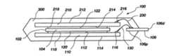
- FIG. 1comprises a side sectional elevation of an exemplary semiconductor die assembly according to the present invention
- FIG. 2comprises a top elevation of the exemplary semiconductor die assembly of FIG. 1 ;
- FIG. 3comprises a side sectional elevation of another exemplary semiconductor die assembly according to the present invention.
- FIG. 4comprises a top elevation of the exemplary semiconductor die assembly of FIG. 3 ;
- FIG. 5comprises a schematic of an electronic system incorporating at least one semiconductor die assembly according to the present invention.
- exemplary semiconductor die assembly 100 configured as a TSOPincludes a substantially planar lead frame 102 including a die paddle 104 and a plurality of lead fingers 106 laterally spaced from die paddle 104 and to one side thereof.
- lead fingers 106may be disposed in a mutually parallel relationship and substantially perpendicular to the proximal side of die paddle 104 , but this is not a requirement of the present invention.
- Lead frame 102may comprise a stamped or etched metal (for example, copper) lead frame, formed as part of a strip including a plurality of identical lead frames by techniques well known to those of ordinary skill in the art. As illustrated in FIG.
- both die paddle 104 and lead fingers 106are initially secured to a peripheral frame element P of the lead frame strip from which the semiconductor die assembly 100 is severed in a so-called trim and form operation, wherein tabs T are severed along the package periphery and the lead fingers 106 are severed at their distal ends 106 d and, optionally, deformed into a configuration for attachment to higher-level packaging.
- First semiconductor die 110 having an active surface 112 , a backside 114 and a row of peripheral bond pads 116 extending along one side thereofis secured by its active surface 112 using a dielectric die attach element 118 to an underside 120 of die paddle 104 .
- first semiconductor die 110may be of greater lateral extent than die paddle 104 and extend therebeyond on all sides. However, it is primarily significant that first semiconductor die 110 extend laterally beyond die paddle 104 adjacent lead fingers 106 for access by a wire bond capillary to bond pads 116 .
- Bond pads 116may be provided in a row along one side of active surface 112 as part of the initial design of first semiconductor die 110 , or may be conventionally rerouted to that location from, for example, an initial central row arrangement using conductive traces formed as part of a so-called redistribution layer.
- Die attach element 118may comprise, for example, an adhesive in the form of, for example, a thermoset or thermoplastic resin applied to die paddle 104 in liquid or other flowable form.
- die attach element 118comprise a segment of dielectric film such as a polyimide, which is commercially offered, among others, as KAPTON® brand film, coated on each side thereof with a pressure-sensitive adhesive.
- Second semiconductor die 210which maybe substantially identical in size, shape and bond pad configuration to first semiconductor die 110 and having an active surface 212 , a backside 214 and a row of peripheral bond pads 216 extending along one side thereof is secured by its backside 214 using a dielectric die attach element 218 to a top side 122 of die paddle 104 .
- second semiconductor die 210may be of greater lateral extent than die paddle 104 and extend therebeyond on all sides. However, this is not a requirement of the present invention.
- Die attach element 218may be, for convenience, identical in size, shape and material or materials to die attach element 118 .
- a plurality of wire bonds 130extends between bond pads 116 of first semiconductor die 110 and lead fingers 106 of the plurality.
- a plurality of wire bonds 230extends between bond pads 216 of second semiconductor die 210 and lead fingers 106 of the plurality.
- one or more wire bonds 130 and one or more wire bonds 230may extend to a common lead finger 106 to provide, for example, power or ground or another bias voltage to both first semiconductor die 110 and second semiconductor die 210 .
- Wire bondsmay be formed using conventional techniques and may comprise, for example, gold, aluminum or alloys thereof. It is currently preferred to use standoff stitch bonding to form wire bonds 130 and conventional low loop bonding to form wire bonds 230 , although the invention is not so limited.
- Encapsulant body 300is formed over die paddle 104 , first semiconductor die 110 , second semiconductor die 210 , wire bonds 130 and 230 , and proximal ends 106 p of lead fingers 106 , distal ends 106 d extending beyond encapsulant body 300 to provide mechanical and electrical coupling for semiconductor die assembly 100 to higher-level packaging.
- Encapsulant body 300may be formed by any suitable technique known in the art, including injection molding and pot molding. However, it is currently preferred that encapsulant body 300 be formed by transfer molding, wherein a thermoplastic, silicon particle-filled resin is heated to a molten state and transferred under pressure through a runner or passage in a mold assembly to a cavity holding semiconductor die assembly 100 .
- Fabrication of semiconductor die assembly 100may be effected by securing first semiconductor die 110 by active surface 112 using die attach element 118 to the underside 120 of die paddle 104 at a location wherein bond pads 116 are exposed beyond the edge of die paddle 104 proximate lead fingers 106 so that adequate clearance is provided for a wire bond capillary. Wire bonds 130 are then selectively formed between bond pads 116 and lead fingers 106 .
- Second semiconductor die 210is then secured by its backside 214 to top side 122 of die paddle 104 using die attach element 218 .
- second semiconductor die 210may be superimposed over first semiconductor die 110 so that the lateral periphery of each die is coextensive with that of the other, and first and second semiconductor dice 110 , 210 are symmetrically disposed with respect to die paddle 104 .
- Such dispositionis not a requirement of the present invention but provides the most compact package and conserves space, or “real estate,” on a carrier substrate, such as a circuit board, if semiconductor die assembly 100 is to be conventionally mounted parallel to the plane of the substrate.
- Wire bonds 230are then selectively formed between bond pads 216 and lead fingers 106 .
- the resulting semiconductor die assembly 100may then be placed in a mold cavity of a transfer molding assembly and encapsulant body 300 formed over die paddle 104 , first semiconductor die 110 , second semiconductor die 210 , wire bonds 130 and 230 , and proximal ends 106 p of lead fingers 106 , with distal ends 106 d extending therebeyond.
- a trim and form operationmay then be conducted, as previously noted, to sever semiconductor die assembly 100 from peripheral frame element P and form distal ends 106 d of lead fingers 106 to a desired configuration.
- another exemplary semiconductor die assembly 400 configured as a QFPincludes a substantially planar lead frame 402 including a die paddle 404 and a plurality of lead fingers 406 laterally spaced from die paddle 404 and comprising a plurality of groups of lead fingers 406 , each group adjacent a side thereof.
- lead fingers 406may be disposed in a mutually parallel relationship and substantially perpendicular to the proximal side of die paddle 404 , but this is not a requirement of the present invention.
- Lead frame 402may comprise a stamped or etched metal (for example, copper) lead frame, formed as part of a strip including a plurality of identical lead frames by techniques well known to those of ordinary skill in the art.
- both die paddle 404 and lead fingers 406are initially secured to a peripheral frame element of the lead frame strip from which the semiconductor die assembly 400 is severed in a so-called trim and form operation and the lead fingers 406 are severed at their distal ends 406 d and, optionally, deformed into a configuration for attachment to higher-level packaging.
- First semiconductor die 410having an active surface 412 , a backside 414 and a plurality of peripheral bond pads 416 in a plurality of groups, each group of bond pads 416 extending along one side of active surface 412 , is secured by its active surface 412 using a dielectric die attach element 418 to an underside 420 of die paddle 404 .
- first semiconductor die 410may be of greater lateral extent than die paddle 404 and extend therebeyond on all sides for access by a wire bond capillary to bond pads 416 .
- Bond pads 416may be provided in a row along each side of active surface 412 as part of the initial design of first semiconductor die 410 , or may be conventionally rerouted to that location from, for example, an initial central row arrangement using conductive traces formed as part of a so-called redistribution layer.
- Die attach element 418may comprise the same material or materials as die attach elements 118 and 218 (see FIG. 2 ).
- Second semiconductor die 510which may be substantially identical in size, shape and bond pad configuration to first semiconductor die 410 and having an active surface 512 , a backside 514 and a row of peripheral bond pads 516 in a plurality of groups, each group of bond pads 516 extending along one side of active surface 512 , is secured by its backside 514 using a dielectric die attach element 518 to a top side 422 of die paddle 404 .
- second semiconductor die 510may be of greater lateral extent than die paddle 404 and extend therebeyond on all sides.
- Die attach element 518may be, for convenience, identical in size, shape and material or materials to die attach element 418 .
- a plurality of wire bonds 430extends between bond pads 416 of first semiconductor die 410 and lead fingers 406 of the plurality.
- a plurality of wire bonds 530extends between bond pads 516 of second semiconductor die 510 and lead fingers 406 of the plurality.
- one or more wire bonds 430 and one or more wire bonds 530may extend to a common lead finger 406 to provide, for example, power or ground or another bias voltage to both first semiconductor die 410 and second semiconductor die 510 .
- Wire bondsmay be formed using conventional techniques and may comprise, for example, gold, aluminum or alloys thereof.
- Encapsulant body 600is formed over die paddle 404 , first semiconductor die 410 , second semiconductor die 510 , the plurality of wire bonds 430 and 530 , and proximal ends 406 p of lead fingers 406 , with distal ends 406 d extending beyond encapsulant body 600 to provide mechanical and electrical coupling for semiconductor die assembly 400 to higher-level packaging.
- Encapsulant body 600may be formed, as in the case of the first embodiment, by transfer molding.
- Fabrication of semiconductor die assembly 400may be effected by securing active surface 412 of first semiconductor die 410 by using die attach element 418 to the underside 420 of die paddle 404 in a symmetrical, superimposed arrangement, wherein bond pads 416 are exposed beyond the edges of die paddle 404 proximate lead fingers 406 so that adequate clearance is provided on all sides of die paddle 404 for a wire bond capillary. Wire bonds 430 are then selectively formed between bond pads 416 and lead fingers 406 .
- Second semiconductor die 510is then secured by its backside 514 to top side 422 of die paddle 404 using die attach element 518 .
- second semiconductor die 510may be superimposed over first semiconductor die 410 so that the lateral periphery of each die is coextensive with that of the other, and first and second semiconductor dice 410 , 510 are symmetrically disposed with respect to die paddle 404 .
- Such dispositionis not a requirement of the present invention but provides the most compact package and conserves space, or “real estate,” on a carrier substrate, such as a circuit board, if semiconductor die assembly 400 is to be conventionally mounted parallel to the plane of the substrate.
- Wire bonds 530are then selectively formed between bond pads 516 and lead fingers 406 .
- the resulting assemblymay then be placed in a mold cavity of a transfer molding assembly and encapsulant body 600 formed over die paddle 404 , first semiconductor die 410 , second semiconductor die 510 , wire bonds 430 and 530 , and proximal ends 406 p of lead fingers 406 , with distal ends 406 d extending therebeyond.
- a trim and form operationmay then be conducted, as previously noted, to sever semiconductor die assembly 400 from the peripheral frame element of the lead frame strip and form distal ends 406 d of lead fingers 406 to a desired configuration.
- FIG. 5is a schematic of an exemplary electronic system 700 , which may be configured, for example, as a personal computer and which incorporates at least one semiconductor die assembly according to the present invention.
- Electronic system 700includes a processor 702 which is operably coupled to one or more input devices 704 such as, for example, a keyboard and a mouse.
- Processor 702is also operably coupled to one or more output devices 706 such as, for example, a display and a printer.
- processor 702is also operably coupled to memory 708 , which may comprise a hard drive and which further incorporates memory in the form of dynamic random access memory (DRAM) comprising semiconductor dice in an assembly 710 according to the present invention.
- Assembly 710may comprise exemplary semiconductor die assembly 100 , exemplary semiconductor die assembly 400 , or any other semiconductor die assembly according to the present invention.
- Assembly 710may further comprise a memory module including a plurality of semiconductor die assemblies according to the present invention.
Landscapes
- Physics & Mathematics (AREA)
- Condensed Matter Physics & Semiconductors (AREA)
- General Physics & Mathematics (AREA)
- Engineering & Computer Science (AREA)
- Computer Hardware Design (AREA)
- Microelectronics & Electronic Packaging (AREA)
- Power Engineering (AREA)
- Die Bonding (AREA)
- Wire Bonding (AREA)
- Lead Frames For Integrated Circuits (AREA)
Abstract
Description
Claims (21)
Priority Applications (2)
| Application Number | Priority Date | Filing Date | Title |
|---|---|---|---|
| US10/652,163US7368320B2 (en) | 2003-08-29 | 2003-08-29 | Method of fabricating a two die semiconductor assembly |
| US11/110,583US7372129B2 (en) | 2003-08-29 | 2005-04-20 | Two die semiconductor assembly and system including same |
Applications Claiming Priority (1)
| Application Number | Priority Date | Filing Date | Title |
|---|---|---|---|
| US10/652,163US7368320B2 (en) | 2003-08-29 | 2003-08-29 | Method of fabricating a two die semiconductor assembly |
Related Child Applications (1)
| Application Number | Title | Priority Date | Filing Date |
|---|---|---|---|
| US11/110,583DivisionUS7372129B2 (en) | 2003-08-29 | 2005-04-20 | Two die semiconductor assembly and system including same |
Publications (2)
| Publication Number | Publication Date |
|---|---|
| US20050046005A1 US20050046005A1 (en) | 2005-03-03 |
| US7368320B2true US7368320B2 (en) | 2008-05-06 |
Family
ID=34217575
Family Applications (2)
| Application Number | Title | Priority Date | Filing Date |
|---|---|---|---|
| US10/652,163Expired - LifetimeUS7368320B2 (en) | 2003-08-29 | 2003-08-29 | Method of fabricating a two die semiconductor assembly |
| US11/110,583Expired - LifetimeUS7372129B2 (en) | 2003-08-29 | 2005-04-20 | Two die semiconductor assembly and system including same |
Family Applications After (1)
| Application Number | Title | Priority Date | Filing Date |
|---|---|---|---|
| US11/110,583Expired - LifetimeUS7372129B2 (en) | 2003-08-29 | 2005-04-20 | Two die semiconductor assembly and system including same |
Country Status (1)
| Country | Link |
|---|---|
| US (2) | US7368320B2 (en) |
Cited By (2)
| Publication number | Priority date | Publication date | Assignee | Title |
|---|---|---|---|---|
| US20070057367A1 (en)* | 2001-07-10 | 2007-03-15 | Samsung Electronics Co., Ltd. | Semiconductor chip having bond pads and multi-chip package |
| US20090051016A1 (en)* | 2007-08-20 | 2009-02-26 | Ivan Galesic | Electronic component with buffer layer |
Families Citing this family (8)
| Publication number | Priority date | Publication date | Assignee | Title |
|---|---|---|---|---|
| US7629695B2 (en) | 2004-05-20 | 2009-12-08 | Kabushiki Kaisha Toshiba | Stacked electronic component and manufacturing method thereof |
| US7381593B2 (en)* | 2004-08-05 | 2008-06-03 | St Assembly Test Services Ltd. | Method and apparatus for stacked die packaging |
| US7816182B2 (en)* | 2004-11-30 | 2010-10-19 | Stmicroelectronics Asia Pacific Pte. Ltd. | Simplified multichip packaging and package design |
| US8211748B2 (en)* | 2006-08-28 | 2012-07-03 | Avago Technologies Ecbu Ip (Singapore) Pte. Ltd. | Systems and methods for low profile die package |
| US7763493B2 (en)* | 2007-06-26 | 2010-07-27 | Stats Chippac Ltd. | Integrated circuit package system with top and bottom terminals |
| US8217511B2 (en)* | 2007-07-31 | 2012-07-10 | Freescale Semiconductor, Inc. | Redistributed chip packaging with thermal contact to device backside |
| US8115286B2 (en)* | 2008-10-22 | 2012-02-14 | Honeywell International Inc. | Integrated sensor including sensing and processing die mounted on opposite sides of package substrate |
| US8400778B2 (en)* | 2010-02-02 | 2013-03-19 | Monolithic Power Systems, Inc. | Layout schemes and apparatus for multi-phase power switch-mode voltage regulator |
Citations (40)
| Publication number | Priority date | Publication date | Assignee | Title |
|---|---|---|---|---|
| JPH0316550A (en) | 1989-06-14 | 1991-01-24 | Matsushita Electric Ind Co Ltd | dishwasher |
| US5157480A (en) | 1991-02-06 | 1992-10-20 | Motorola, Inc. | Semiconductor device having dual electrical contact sites |
| US5366933A (en) | 1993-10-13 | 1994-11-22 | Intel Corporation | Method for constructing a dual sided, wire bonded integrated circuit chip package |
| US5422435A (en) | 1992-05-22 | 1995-06-06 | National Semiconductor Corporation | Stacked multi-chip modules and method of manufacturing |
| US5677569A (en) | 1994-10-27 | 1997-10-14 | Samsung Electronics Co., Ltd. | Semiconductor multi-package stack |
| US5777345A (en) | 1996-01-03 | 1998-07-07 | Intel Corporation | Multi-chip integrated circuit package |
| US5793101A (en) | 1995-03-13 | 1998-08-11 | Intel Corporation | Package housing multiple semiconductor dies |
| US6005778A (en) | 1995-06-15 | 1999-12-21 | Honeywell Inc. | Chip stacking and capacitor mounting arrangement including spacers |
| US6037661A (en) | 1996-12-20 | 2000-03-14 | International Business Machines | Multichip module |
| US6072243A (en)* | 1996-11-26 | 2000-06-06 | Sharp Kabushiki Kaisha | Semiconductor integrated circuit device capable of surely electrically insulating two semiconductor chips from each other and fabricating method thereof |
| US6114752A (en) | 1998-11-10 | 2000-09-05 | Siliconware Precision Industries Co., Ltd. | Semiconductor package having lead frame with an exposed base pad |
| US6133637A (en)* | 1997-01-24 | 2000-10-17 | Rohm Co., Ltd. | Semiconductor device having a plurality of semiconductor chips |
| US6140154A (en)* | 1996-10-25 | 2000-10-31 | Micron Technology, Inc. | Multi-part lead frame with dissimilar materials and method of manufacturing |
| US6175149B1 (en) | 1998-02-13 | 2001-01-16 | Micron Technology, Inc. | Mounting multiple semiconductor dies in a package |
| US6197615B1 (en)* | 1997-04-04 | 2001-03-06 | Samsung Electronics Co., Ltd. | Method of producing lead frame having uneven surfaces |
| US6265760B1 (en)* | 1998-05-01 | 2001-07-24 | Nec Corporation | Semiconductor device, and semiconductor device with die pad and protruding chip lead frame and method of manufacturing the same |
| US6297547B1 (en) | 1998-02-13 | 2001-10-02 | Micron Technology Inc. | Mounting multiple semiconductor dies in a package |
| US6303981B1 (en)* | 1999-09-01 | 2001-10-16 | Micron Technology, Inc. | Semiconductor package having stacked dice and leadframes and method of fabrication |
| US6313527B1 (en)* | 1998-12-10 | 2001-11-06 | United Microelectronics Corp. | Dual-dies packaging structure and packaging method |
| JP2001332684A (en) | 2000-05-22 | 2001-11-30 | Mitsubishi Electric Corp | Resin-sealed semiconductor device and method of manufacturing the same |
| US6333549B2 (en)* | 1998-03-06 | 2001-12-25 | Microchip Technology Incorporated | Integrated circuit package having interchip bonding and method therefor |
| US6337521B1 (en)* | 1999-09-22 | 2002-01-08 | Hitachi, Ltd. | Semiconductor device and a method of manufacturing the same |
| US6437447B1 (en) | 2000-09-06 | 2002-08-20 | Siliconware Precision Industries Co., Ltd. | Dual-sided chip package without a die pad |
| US6476474B1 (en)* | 2000-10-10 | 2002-11-05 | Siliconware Precision Industries Co., Ltd. | Dual-die package structure and method for fabricating the same |
| US6479323B1 (en)* | 1995-09-19 | 2002-11-12 | National Semiconductor Corporation | Method for attaching a lead frame to a heat spreader/heat slug structure |
| US6483181B2 (en) | 2001-04-19 | 2002-11-19 | Walton Advanced Electronics Ltd. | Multi-chip package |
| US6528408B2 (en)* | 2001-05-21 | 2003-03-04 | Micron Technology, Inc. | Method for bumped die and wire bonded board-on-chip package |
| US6552416B1 (en)* | 2000-09-08 | 2003-04-22 | Amkor Technology, Inc. | Multiple die lead frame package with enhanced die-to-die interconnect routing using internal lead trace wiring |
| US6555902B2 (en)* | 2000-07-17 | 2003-04-29 | Siliconware Precision Industries Co., Ltd. | Multiple stacked-chip packaging structure |
| US6680531B2 (en)* | 2001-09-13 | 2004-01-20 | Siliconware Precision Industries Co., Ltd. | Multi-chip semiconductor package |
| US6692991B2 (en)* | 2001-12-05 | 2004-02-17 | Matsushita Electric Industrial Co., Ltd. | Resin-encapsulated semiconductor device and method for manufacturing the same |
| US6700206B2 (en)* | 2002-08-02 | 2004-03-02 | Micron Technology, Inc. | Stacked semiconductor package and method producing same |
| US20040251557A1 (en)* | 2003-06-16 | 2004-12-16 | Sandisk Corporation | Integrated circuit package having stacked integrated circuits and method therefor |
| US20050026325A1 (en)* | 2002-08-08 | 2005-02-03 | Koon Eng Meow | Packaged microelectronic components |
| US20050121802A1 (en) | 2003-11-28 | 2005-06-09 | Nec Electronics Corporation | Offset-bonded, multi-chip semiconductor device |
| US6951982B2 (en)* | 2002-11-22 | 2005-10-04 | Micron Technology, Inc. | Packaged microelectronic component assemblies |
| US7023076B2 (en)* | 2002-07-18 | 2006-04-04 | United Test & Assembly Center Limited | Multiple chip semiconductor packages |
| US20060255436A1 (en)* | 2005-05-11 | 2006-11-16 | Isao Ozawa | Semiconductor device with sealed semiconductor chip |
| US20070025684A1 (en)* | 2005-07-28 | 2007-02-01 | Ralf Otremba | Connection Structure Semiconductor Chip and Electronic Component Including the Connection Structure and Methods for Producing the Connection Structure |
| US20070194463A1 (en) | 2006-02-21 | 2007-08-23 | Young Cheol Kim | Integrated circuit package system with l-shaped leadfingers |
Family Cites Families (1)
| Publication number | Priority date | Publication date | Assignee | Title |
|---|---|---|---|---|
| SG97938A1 (en)* | 2000-09-21 | 2003-08-20 | Micron Technology Inc | Method to prevent die attach adhesive contamination in stacked chips |
- 2003
- 2003-08-29USUS10/652,163patent/US7368320B2/ennot_activeExpired - Lifetime
- 2005
- 2005-04-20USUS11/110,583patent/US7372129B2/ennot_activeExpired - Lifetime
Patent Citations (41)
| Publication number | Priority date | Publication date | Assignee | Title |
|---|---|---|---|---|
| JPH0316550A (en) | 1989-06-14 | 1991-01-24 | Matsushita Electric Ind Co Ltd | dishwasher |
| US5157480A (en) | 1991-02-06 | 1992-10-20 | Motorola, Inc. | Semiconductor device having dual electrical contact sites |
| US5422435A (en) | 1992-05-22 | 1995-06-06 | National Semiconductor Corporation | Stacked multi-chip modules and method of manufacturing |
| US5502289A (en)* | 1992-05-22 | 1996-03-26 | National Semiconductor Corporation | Stacked multi-chip modules and method of manufacturing |
| US5366933A (en) | 1993-10-13 | 1994-11-22 | Intel Corporation | Method for constructing a dual sided, wire bonded integrated circuit chip package |
| US5677569A (en) | 1994-10-27 | 1997-10-14 | Samsung Electronics Co., Ltd. | Semiconductor multi-package stack |
| US5793101A (en) | 1995-03-13 | 1998-08-11 | Intel Corporation | Package housing multiple semiconductor dies |
| US6005778A (en) | 1995-06-15 | 1999-12-21 | Honeywell Inc. | Chip stacking and capacitor mounting arrangement including spacers |
| US6479323B1 (en)* | 1995-09-19 | 2002-11-12 | National Semiconductor Corporation | Method for attaching a lead frame to a heat spreader/heat slug structure |
| US5777345A (en) | 1996-01-03 | 1998-07-07 | Intel Corporation | Multi-chip integrated circuit package |
| US6140154A (en)* | 1996-10-25 | 2000-10-31 | Micron Technology, Inc. | Multi-part lead frame with dissimilar materials and method of manufacturing |
| US6072243A (en)* | 1996-11-26 | 2000-06-06 | Sharp Kabushiki Kaisha | Semiconductor integrated circuit device capable of surely electrically insulating two semiconductor chips from each other and fabricating method thereof |
| US6037661A (en) | 1996-12-20 | 2000-03-14 | International Business Machines | Multichip module |
| US6133637A (en)* | 1997-01-24 | 2000-10-17 | Rohm Co., Ltd. | Semiconductor device having a plurality of semiconductor chips |
| US6197615B1 (en)* | 1997-04-04 | 2001-03-06 | Samsung Electronics Co., Ltd. | Method of producing lead frame having uneven surfaces |
| US6175149B1 (en) | 1998-02-13 | 2001-01-16 | Micron Technology, Inc. | Mounting multiple semiconductor dies in a package |
| US6297547B1 (en) | 1998-02-13 | 2001-10-02 | Micron Technology Inc. | Mounting multiple semiconductor dies in a package |
| US6333549B2 (en)* | 1998-03-06 | 2001-12-25 | Microchip Technology Incorporated | Integrated circuit package having interchip bonding and method therefor |
| US6265760B1 (en)* | 1998-05-01 | 2001-07-24 | Nec Corporation | Semiconductor device, and semiconductor device with die pad and protruding chip lead frame and method of manufacturing the same |
| US6114752A (en) | 1998-11-10 | 2000-09-05 | Siliconware Precision Industries Co., Ltd. | Semiconductor package having lead frame with an exposed base pad |
| US6313527B1 (en)* | 1998-12-10 | 2001-11-06 | United Microelectronics Corp. | Dual-dies packaging structure and packaging method |
| US6303981B1 (en)* | 1999-09-01 | 2001-10-16 | Micron Technology, Inc. | Semiconductor package having stacked dice and leadframes and method of fabrication |
| US6337521B1 (en)* | 1999-09-22 | 2002-01-08 | Hitachi, Ltd. | Semiconductor device and a method of manufacturing the same |
| JP2001332684A (en) | 2000-05-22 | 2001-11-30 | Mitsubishi Electric Corp | Resin-sealed semiconductor device and method of manufacturing the same |
| US6555902B2 (en)* | 2000-07-17 | 2003-04-29 | Siliconware Precision Industries Co., Ltd. | Multiple stacked-chip packaging structure |
| US6437447B1 (en) | 2000-09-06 | 2002-08-20 | Siliconware Precision Industries Co., Ltd. | Dual-sided chip package without a die pad |
| US6552416B1 (en)* | 2000-09-08 | 2003-04-22 | Amkor Technology, Inc. | Multiple die lead frame package with enhanced die-to-die interconnect routing using internal lead trace wiring |
| US6476474B1 (en)* | 2000-10-10 | 2002-11-05 | Siliconware Precision Industries Co., Ltd. | Dual-die package structure and method for fabricating the same |
| US6483181B2 (en) | 2001-04-19 | 2002-11-19 | Walton Advanced Electronics Ltd. | Multi-chip package |
| US6528408B2 (en)* | 2001-05-21 | 2003-03-04 | Micron Technology, Inc. | Method for bumped die and wire bonded board-on-chip package |
| US6680531B2 (en)* | 2001-09-13 | 2004-01-20 | Siliconware Precision Industries Co., Ltd. | Multi-chip semiconductor package |
| US6692991B2 (en)* | 2001-12-05 | 2004-02-17 | Matsushita Electric Industrial Co., Ltd. | Resin-encapsulated semiconductor device and method for manufacturing the same |
| US7023076B2 (en)* | 2002-07-18 | 2006-04-04 | United Test & Assembly Center Limited | Multiple chip semiconductor packages |
| US6700206B2 (en)* | 2002-08-02 | 2004-03-02 | Micron Technology, Inc. | Stacked semiconductor package and method producing same |
| US20050026325A1 (en)* | 2002-08-08 | 2005-02-03 | Koon Eng Meow | Packaged microelectronic components |
| US6951982B2 (en)* | 2002-11-22 | 2005-10-04 | Micron Technology, Inc. | Packaged microelectronic component assemblies |
| US20040251557A1 (en)* | 2003-06-16 | 2004-12-16 | Sandisk Corporation | Integrated circuit package having stacked integrated circuits and method therefor |
| US20050121802A1 (en) | 2003-11-28 | 2005-06-09 | Nec Electronics Corporation | Offset-bonded, multi-chip semiconductor device |
| US20060255436A1 (en)* | 2005-05-11 | 2006-11-16 | Isao Ozawa | Semiconductor device with sealed semiconductor chip |
| US20070025684A1 (en)* | 2005-07-28 | 2007-02-01 | Ralf Otremba | Connection Structure Semiconductor Chip and Electronic Component Including the Connection Structure and Methods for Producing the Connection Structure |
| US20070194463A1 (en) | 2006-02-21 | 2007-08-23 | Young Cheol Kim | Integrated circuit package system with l-shaped leadfingers |
Cited By (4)
| Publication number | Priority date | Publication date | Assignee | Title |
|---|---|---|---|---|
| US20070057367A1 (en)* | 2001-07-10 | 2007-03-15 | Samsung Electronics Co., Ltd. | Semiconductor chip having bond pads and multi-chip package |
| US7576440B2 (en)* | 2001-07-10 | 2009-08-18 | Samsung Electronics Co., Ltd. | Semiconductor chip having bond pads and multi-chip package |
| US20090051016A1 (en)* | 2007-08-20 | 2009-02-26 | Ivan Galesic | Electronic component with buffer layer |
| US8283756B2 (en)* | 2007-08-20 | 2012-10-09 | Infineon Technologies Ag | Electronic component with buffer layer |
Also Published As
| Publication number | Publication date |
|---|---|
| US7372129B2 (en) | 2008-05-13 |
| US20050046005A1 (en) | 2005-03-03 |
| US20050184367A1 (en) | 2005-08-25 |
Similar Documents
| Publication | Publication Date | Title |
|---|---|---|
| JP3170182B2 (en) | Resin-sealed semiconductor device and method of manufacturing the same | |
| US8836101B2 (en) | Multi-chip semiconductor packages and assembly thereof | |
| JP3332516B2 (en) | Thermally enhanced semiconductor device having exposed back surface and method of manufacturing the same | |
| US6803258B2 (en) | Semiconductor device | |
| US20100193922A1 (en) | Semiconductor chip package | |
| JPH0878605A (en) | Lead frame and semiconductor integrated circuit device using the same | |
| US7642638B2 (en) | Inverted lead frame in substrate | |
| US20060226521A1 (en) | Semiconductor Package Having Integrated Metal Parts for Thermal Enhancement | |
| KR101440933B1 (en) | Integrated circuit package system employing bump technology | |
| JP3837215B2 (en) | Individual semiconductor device and manufacturing method thereof | |
| JP2001237361A (en) | Lead frame having small lifting mount pad | |
| US7368320B2 (en) | Method of fabricating a two die semiconductor assembly | |
| TWI292213B (en) | ||
| US20080073763A1 (en) | Semiconductor device and method of manufacturing the same | |
| US20050073032A1 (en) | Leadless semiconductor package | |
| JPH0722454A (en) | Semiconductor integrated circuit device | |
| CN107305879B (en) | Semiconductor device and corresponding method | |
| JPH07161876A (en) | SEMICONDUCTOR INTEGRATED CIRCUIT DEVICE, METHOD FOR MANUFACTURING THE SAME, AND MOLD DIES USED FOR MANUFACTURING THE SAME | |
| US8053285B2 (en) | Thermally enhanced single inline package (SIP) | |
| JP2682200B2 (en) | Semiconductor device | |
| JP2663860B2 (en) | Resin-sealed semiconductor device | |
| JP2814006B2 (en) | Substrate for mounting electronic components | |
| JPH11219969A (en) | Semiconductor device | |
| JPH02180061A (en) | Lead frames and semiconductor devices | |
| KR100230920B1 (en) | Semiconductor package |
Legal Events
| Date | Code | Title | Description |
|---|---|---|---|
| AS | Assignment | Owner name:MICRON TECHNOLOGY, INC., IDAHO Free format text:ASSIGNMENT OF ASSIGNORS INTEREST;ASSIGNOR:BOWEN, NEAL;REEL/FRAME:014463/0660 Effective date:20030818 | |
| FEPP | Fee payment procedure | Free format text:PAYOR NUMBER ASSIGNED (ORIGINAL EVENT CODE: ASPN); ENTITY STATUS OF PATENT OWNER: LARGE ENTITY | |
| STCF | Information on status: patent grant | Free format text:PATENTED CASE | |
| FPAY | Fee payment | Year of fee payment:4 | |
| FPAY | Fee payment | Year of fee payment:8 | |
| AS | Assignment | Owner name:U.S. BANK NATIONAL ASSOCIATION, AS COLLATERAL AGENT, CALIFORNIA Free format text:SECURITY INTEREST;ASSIGNOR:MICRON TECHNOLOGY, INC.;REEL/FRAME:038669/0001 Effective date:20160426 Owner name:U.S. BANK NATIONAL ASSOCIATION, AS COLLATERAL AGEN Free format text:SECURITY INTEREST;ASSIGNOR:MICRON TECHNOLOGY, INC.;REEL/FRAME:038669/0001 Effective date:20160426 | |
| AS | Assignment | Owner name:MORGAN STANLEY SENIOR FUNDING, INC., AS COLLATERAL AGENT, MARYLAND Free format text:PATENT SECURITY AGREEMENT;ASSIGNOR:MICRON TECHNOLOGY, INC.;REEL/FRAME:038954/0001 Effective date:20160426 Owner name:MORGAN STANLEY SENIOR FUNDING, INC., AS COLLATERAL Free format text:PATENT SECURITY AGREEMENT;ASSIGNOR:MICRON TECHNOLOGY, INC.;REEL/FRAME:038954/0001 Effective date:20160426 | |
| AS | Assignment | Owner name:U.S. BANK NATIONAL ASSOCIATION, AS COLLATERAL AGENT, CALIFORNIA Free format text:CORRECTIVE ASSIGNMENT TO CORRECT THE REPLACE ERRONEOUSLY FILED PATENT #7358718 WITH THE CORRECT PATENT #7358178 PREVIOUSLY RECORDED ON REEL 038669 FRAME 0001. ASSIGNOR(S) HEREBY CONFIRMS THE SECURITY INTEREST;ASSIGNOR:MICRON TECHNOLOGY, INC.;REEL/FRAME:043079/0001 Effective date:20160426 Owner name:U.S. BANK NATIONAL ASSOCIATION, AS COLLATERAL AGEN Free format text:CORRECTIVE ASSIGNMENT TO CORRECT THE REPLACE ERRONEOUSLY FILED PATENT #7358718 WITH THE CORRECT PATENT #7358178 PREVIOUSLY RECORDED ON REEL 038669 FRAME 0001. ASSIGNOR(S) HEREBY CONFIRMS THE SECURITY INTEREST;ASSIGNOR:MICRON TECHNOLOGY, INC.;REEL/FRAME:043079/0001 Effective date:20160426 | |
| AS | Assignment | Owner name:JPMORGAN CHASE BANK, N.A., AS COLLATERAL AGENT, ILLINOIS Free format text:SECURITY INTEREST;ASSIGNORS:MICRON TECHNOLOGY, INC.;MICRON SEMICONDUCTOR PRODUCTS, INC.;REEL/FRAME:047540/0001 Effective date:20180703 Owner name:JPMORGAN CHASE BANK, N.A., AS COLLATERAL AGENT, IL Free format text:SECURITY INTEREST;ASSIGNORS:MICRON TECHNOLOGY, INC.;MICRON SEMICONDUCTOR PRODUCTS, INC.;REEL/FRAME:047540/0001 Effective date:20180703 | |
| AS | Assignment | Owner name:MICRON TECHNOLOGY, INC., IDAHO Free format text:RELEASE BY SECURED PARTY;ASSIGNOR:U.S. BANK NATIONAL ASSOCIATION, AS COLLATERAL AGENT;REEL/FRAME:047243/0001 Effective date:20180629 | |
| AS | Assignment | Owner name:MICRON TECHNOLOGY, INC., IDAHO Free format text:RELEASE BY SECURED PARTY;ASSIGNOR:MORGAN STANLEY SENIOR FUNDING, INC., AS COLLATERAL AGENT;REEL/FRAME:050937/0001 Effective date:20190731 | |
| MAFP | Maintenance fee payment | Free format text:PAYMENT OF MAINTENANCE FEE, 12TH YEAR, LARGE ENTITY (ORIGINAL EVENT CODE: M1553); ENTITY STATUS OF PATENT OWNER: LARGE ENTITY Year of fee payment:12 | |
| AS | Assignment | Owner name:MICRON SEMICONDUCTOR PRODUCTS, INC., IDAHO Free format text:RELEASE BY SECURED PARTY;ASSIGNOR:JPMORGAN CHASE BANK, N.A., AS COLLATERAL AGENT;REEL/FRAME:051028/0001 Effective date:20190731 Owner name:MICRON TECHNOLOGY, INC., IDAHO Free format text:RELEASE BY SECURED PARTY;ASSIGNOR:JPMORGAN CHASE BANK, N.A., AS COLLATERAL AGENT;REEL/FRAME:051028/0001 Effective date:20190731 |