US7366942B2 - Method and apparatus for high-speed input sampling - Google Patents
Method and apparatus for high-speed input samplingDownload PDFInfo
- Publication number
- US7366942B2 US7366942B2US10/918,008US91800804AUS7366942B2US 7366942 B2US7366942 B2US 7366942B2US 91800804 AUS91800804 AUS 91800804AUS 7366942 B2US7366942 B2US 7366942B2
- Authority
- US
- United States
- Prior art keywords
- signal
- clock
- input
- voltage
- data
- Prior art date
- Legal status (The legal status is an assumption and is not a legal conclusion. Google has not performed a legal analysis and makes no representation as to the accuracy of the status listed.)
- Expired - Fee Related, expires
Links
- 238000005070samplingMethods0.000titleclaimsabstractdescription37
- 238000000034methodMethods0.000titleclaimsabstractdescription27
- 239000004065semiconductorSubstances0.000claimsabstractdescription26
- 230000000630rising effectEffects0.000claimsabstractdescription18
- 239000000872bufferSubstances0.000claimsdescription59
- 230000007704transitionEffects0.000claimsdescription54
- 230000003139buffering effectEffects0.000claimsdescription18
- 238000011156evaluationMethods0.000abstractdescription6
- 230000001934delayEffects0.000description18
- 238000010586diagramMethods0.000description8
- 239000000758substrateSubstances0.000description6
- 238000013461designMethods0.000description5
- XUIMIQQOPSSXEZ-UHFFFAOYSA-NSiliconChemical compound[Si]XUIMIQQOPSSXEZ-UHFFFAOYSA-N0.000description4
- 230000009977dual effectEffects0.000description4
- 229910052710siliconInorganic materials0.000description4
- 239000010703siliconSubstances0.000description4
- 238000004891communicationMethods0.000description3
- 229910052751metalInorganic materials0.000description3
- 239000002184metalSubstances0.000description3
- 230000001960triggered effectEffects0.000description3
- 238000001514detection methodMethods0.000description2
- 238000000638solvent extractionMethods0.000description2
- JBRZTFJDHDCESZ-UHFFFAOYSA-NAsGaChemical compound[As]#[Ga]JBRZTFJDHDCESZ-UHFFFAOYSA-N0.000description1
- 229910001218Gallium arsenideInorganic materials0.000description1
- GPXJNWSHGFTCBW-UHFFFAOYSA-NIndium phosphideChemical compound[In]#PGPXJNWSHGFTCBW-UHFFFAOYSA-N0.000description1
- 239000004020conductorSubstances0.000description1
- 230000006870functionEffects0.000description1
- 239000011521glassSubstances0.000description1
- 239000012212insulatorSubstances0.000description1
- 230000015654memoryEffects0.000description1
- 238000012545processingMethods0.000description1
- 238000009877renderingMethods0.000description1
- 229910052594sapphireInorganic materials0.000description1
- 239000010980sapphireSubstances0.000description1
- 230000003068static effectEffects0.000description1
- 238000012546transferMethods0.000description1
Images


Classifications
- H—ELECTRICITY
- H03—ELECTRONIC CIRCUITRY
- H03K—PULSE TECHNIQUE
- H03K5/00—Manipulating of pulses not covered by one of the other main groups of this subclass
- H03K5/13—Arrangements having a single output and transforming input signals into pulses delivered at desired time intervals
- H03K5/135—Arrangements having a single output and transforming input signals into pulses delivered at desired time intervals by the use of time reference signals, e.g. clock signals
- H—ELECTRICITY
- H03—ELECTRONIC CIRCUITRY
- H03K—PULSE TECHNIQUE
- H03K5/00—Manipulating of pulses not covered by one of the other main groups of this subclass
- H03K5/153—Arrangements in which a pulse is delivered at the instant when a predetermined characteristic of an input signal is present or at a fixed time interval after this instant
- G—PHYSICS
- G11—INFORMATION STORAGE
- G11C—STATIC STORES
- G11C27/00—Electric analogue stores, e.g. for storing instantaneous values
- G11C27/02—Sample-and-hold arrangements
- H—ELECTRICITY
- H03—ELECTRONIC CIRCUITRY
- H03K—PULSE TECHNIQUE
- H03K3/00—Circuits for generating electric pulses; Monostable, bistable or multistable circuits
- H03K3/02—Generators characterised by the type of circuit or by the means used for producing pulses
- H03K3/027—Generators characterised by the type of circuit or by the means used for producing pulses by the use of logic circuits, with internal or external positive feedback
- H03K3/037—Bistable circuits
- H—ELECTRICITY
- H03—ELECTRONIC CIRCUITRY
- H03K—PULSE TECHNIQUE
- H03K5/00—Manipulating of pulses not covered by one of the other main groups of this subclass
- H03K5/153—Arrangements in which a pulse is delivered at the instant when a predetermined characteristic of an input signal is present or at a fixed time interval after this instant
- H03K5/1534—Transition or edge detectors
Definitions
- This inventionrelates generally to semiconductor integrated circuits and, more particularly, to high-speed input circuits.
- DDRDouble Data Rate
- DRAMDynamic Random Access Memory
- the valid data window of a signaldefined from an output driver perspective is the period of time a signal may be valid after factoring in variable system parameters, such as process, temperature, voltage, and output loading.
- This valid data windowis generally expressed in terms of a minimum propagation delay and a maximum propagation delay.
- the required data window, or sampling window, from an input sampling perspectiveis defined by the required time that the signal must be valid at the sampler prior to arrival of an active edge of the clock (i.e., setup time) and the required time that the signal must be held valid at the sampler after the active edge of the sampling clock (i.e., hold time).
- the valid data window and the sampling windowcombine to constrain the maximum operating frequency of a system. Reducing the sampling window will allow higher clock frequencies and allow more tolerance in system design parameters.
- any divergence between how the signals are treated prior to arriving at a samplersuch as a flip-flop, widen the sampling window due to delay differences caused by buffers, routing, process, temperature and voltage variations. This is particularly true with clock signals, which may have large fan-out loads and require significant buffering to drive those loads.
- PLLPhase Locked Loop
- DLLDelay Locked Loop
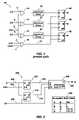
- a sampling circuit 90that does not incorporate a PLL or DLL may be similar to that shown in FIG. 1 .
- a differential buffer 40sensing transitions on an input clock 2 and an inverted input clock 4 generates an internal clock 12 .
- the differential buffer 40is used to enhance detection of a transition point by comparing the voltage on the input clock 2 to the voltage on the inverted input clock 4 .
- a bus of data inputs 6 signals, D 0 through Dnis passed through a set of differential buffers 10 , one for each data input 6 , used for sensing transitions on the data inputs 6 .
- the differential buffers 10include one input connected to a voltage reference signal 8 .
- the use of differential buffers 10allows for faster sensing of input signal transitions, and lower voltage swings on the data inputs 6 .
- the voltage reference signal 8allows setting a voltage value where the transition is considered to have occurred.
- the sensed data signalsmay pass through matched delays 50 .
- these matched delays 50may include active delay components, such as inverters, or may simply be metal routing lines used to delay the signal before arrival at the flip-flops 60 .
- These matched delays 50may be used to delay the signal by an amount similar to the delay on the internal clock 12 .
- FIG. 1 embodiment of a sampling circuit 90reduces the sampling window.
- new circuitry and methodsare needed to accurately receive and sample these communication signals with even smaller sampling windows.
- the present inventionincludes a method of sampling a high-speed signal and a signal sampler for sampling a high-speed signal by creating a reduced sampling window on the signal relative to a received clock signal, which may allow a system to operate at higher clock frequencies and allow more tolerance in system design.
- An embodiment of the present inventioncomprises a signal sampler including a first sampler, which may be a conventional flip-flop, configured to sample a data signal at an active transition of a clock signal and generate a first sampled signal.
- a second samplerwhich may also be a conventional flip-flop, is configured to sample the data signal at an active transition of an inverted clock signal and generate a second sampled signal.
- the active transition of the clock and the active transition of the inverted clockmay be substantially close in time so that the sampling time of the first sampler and the second sampler are substantially close.
- the outputs from the first sampler and the second samplerare operably coupled to an evaluator, which generates an output signal on the next active transition of the clock based on an evaluation of the first sampled signal, the second sampled signal, and a previous logic state of the output signal.
- the output signal generated by the evaluatorwill have that same logic level.
- the output signal generated by the evaluatorwill transition to the opposite logic level from its previous logic state.
- Another embodiment of the present inventioncomprises a method of sampling a signal.
- the methodcomprises sampling a data signal at an active transition of a clock to generate a first sampled signal, sampling the data signal at an active transition of an inverted clock to generate a second sampled signal, and generating an output signal at the active transition of the clock by evaluating the first sampled signal, the second sampled signal, and a previous logic state of the output signal.
- the evaluatingincludes asserting the output signal if the first sampled signal is asserted and the second sampled signal is asserted, negating the output signal if the first sampled signal is negated and the second sampled signal is negated, and toggling the output signal if the first sampled signal and the second sampled signal are in opposite logic states.
- Another embodiment of the present inventioncomprises a semiconductor device including at least one signal sampler according to the invention described herein.
- Another embodiment of the present inventionincludes at least one semiconductor device including at least one signal sampler according to the present invention fabricated on a semiconductor wafer.
- Yet another embodimentin accordance with the present invention, comprises an electronic system including at least one input device, at least one output device, at least one processor and at least one memory device.
- the at least one memory devicecomprises at least one semiconductor memory incorporating at least one signal sampler according to the present invention.
- FIG. 1is a block diagram of a conventional signal sampling implementation
- FIG. 2is a block diagram of an exemplary signal sampler according to the present invention.
- FIG. 3is a block diagram of an exemplary application of the signal sampler showing dual differential clock buffers using a voltage reference for generating a clock signal and an inverted clock signal;
- FIG. 4is a block diagram of an exemplary application of the signal sampler showing dual differential clock buffers for generating a clock signal and an inverted clock signal;
- FIG. 5is a block diagram of an exemplary application of the signal sampler showing differential buffers for data inputs and dual differential clock buffers for generating a clock signal and an inverted clock signal;
- FIG. 6is a block diagram of an exemplary application of the signal sampler showing a clock buffer for generating a clock signal and an inverted clock signal;
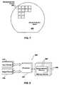
- FIG. 7is a schematic depiction of a semiconductor wafer including a plurality of semiconductor devices including a signal sampler according to the present invention.
- FIG. 8is an electronic system diagram showing a plurality of semiconductor memories including a signal sampler according to the present invention.
- circuits and functionsmay be shown in block diagram form in order not to obscure the present invention in unnecessary detail. Conversely, specific circuit implementations shown and described are exemplary only and should not be construed as the only way to implement the present invention unless specified otherwise herein. Additionally, block definitions and partitioning of logic between various blocks is exemplary of a specific implementation. It will be readily apparent to one of ordinary skill in the art that the present invention may be practiced by numerous other partitioning solutions. For the most part, details concerning timing considerations and the like have been omitted where such details are not necessary to obtain a complete understanding of the present invention and are within the abilities of persons of ordinary skill in the relevant art.
- busis used to refer to a plurality of signals or conductors, which may be used to transfer one or more various types of information, such as data, addresses, control, or status. Additionally, a bus or collection of signals may be referred to in the singular as a signal.
- assertand “negate” are respectively used when referring to the rendering of a signal, status bit, or similar apparatus into its logically true or logically false state. Accordingly, if a logic level one or a high voltage represents a logically true state (i.e., asserted state), a logic level zero or a low voltage will represent the logically false state (i.e., negated state). Conversely, if a logic level zero or a low voltage represents the logically true state (i.e., asserted state), a logic level one or a high voltage will represent the logically false state (i.e., negated state).
- data signalis used to indicate a signal to be sampled by one or more clocks. It will be readily apparent to those skilled in the art that the present invention may apply to any type of communication signal to be sampled. Therefore, the term “data signal” may apply to any signal to be sampled, such as, for example only, data signals, address signals, control, signals, status signals, and timing signals. Additionally, many of the drawings illustrate a bus of data signals. This is done to illustrate that many of the methods of the present invention may be applied across a wide bus of similar signal types, such as a data bus. However, the present invention may be implemented on any number of data signals including a single data signal.
- Uncertainty between arrival time of a data signal relative to arrival time of a clock at a sampling circuitreduces the sampling window of the data signal.
- a data valid window size and position relative to a sampling clock active edgemay be affected by a variety of factors.
- the conventional sampling circuit shown in FIG. 1may address a portion of factors 1) and 2) by inserting a matched delay in the data signal line in an effort to match the data delay to a value similar to the clock delay.
- factors 1) and 2)may be more fully addressed by the present invention.
- the FIG. 1 conventional circuitrydoes not address factors 3) and 4).
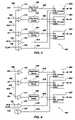
- FIG. 2illustrates a signal sampler 200 according to the present invention.
- the signal sampler 200includes a first sampler 210 , a second sampler 220 and an evaluator 240 .
- the first sampler 210is shown as a rising edge triggered flip-flop (rFF) and the second sampler 220 is shown as a falling edge triggered flip-flop (fFF).
- the evaluator 240is shown as containing evaluation logic and a rising edge triggered flip-flop.
- the active transitioni.e., rising edge or falling edge
- FIG. 2for the convenience of explanation.
- the signal sampler 200may be implemented with the first sampler 210 and evaluator 240 using a falling edge as the active transition rather than a rising edge and the second sampler 220 using a rising edge as the active transition rather than a falling edge. Therefore, for general discussion it may be more convenient to refer to an active edge, or active transition, while for discussions specific to FIG. 2 it may be more convenient to discuss a rising edge of the clock 202 and a falling edge of the inverted clock 204 .
- the rising edge of the clock 202 and the falling edge of the inverted clock 204will be substantially close to each other but may not match exactly. Routing and buffering differences between the clock 202 and the inverted clock 204 prior to reaching the signal sampler 200 may cause minor timing mismatches in these two signals. In addition, as noted in factors 1) and 2) above, routing and buffering differences between the data signal 206 and the clock signals 202 and 204 may cause timing mismatches between the data signal 206 and the clock signals 202 and 204 reducing the data sampling window at the signal sampler 200 .
- the data signal 206 , the clock 202 and the inverted clock 204may all have rise times and rising propagation delays that differ from fall times and falling propagation delays as noted in factor 4) above.
- the falling propagation delay of a signalmay be faster than the rising propagation delay.
- a buffermay be designed to have faster falling times than rising times, even if the process parameters are well matched, due to layout constraints or other considerations.
- the present inventioncompensates for this rising time versus falling time mismatch by using the second sampler 220 to capture the data signal 206 on a falling edge of the inverted clock 204 , which may more closely match the falling edge of the data signal 206 .
- the first sampler 210using a rising edge on the clock 202 , may more closely match the rising edge of the data signal 206 .
- the resulting first sampled signal 216 and second sampled signal 226are connected to the evaluator 240 to determine a final sampled value on an output signal 250 .
- a truth table 270 shown in FIG. 2defines the evaluation logic. If both the first sampled signal 216 and the second sampled signal 226 are at the same logic value, then that logic value will be used as the output signal 250 on the next active edge of the clock 202 . In other words, if both the first sampled signal 216 and the second sampled signal 226 are low (as shown on the first line of the truth table 270 ), then the output signal 250 will be low on the next active edge of the clock 202 . Conversely, if both the first sampled signal 216 and the second sampled signal 226 are high (as shown on the second line of the truth table 270 ), then the output signal 250 will be high on the next active edge of the clock 202 .
- first sampled signal 216 and the second sampled signal 226are in opposite logic states. If this is the case, it may be safe to assume that the data signal 206 transitioned. If no data signal 206 transition occurs, abundant set up time exists in which the data signal 206 is valid before the active edge of the clock 202 and the active edge of the inverted clock 204 . In other words, both the first sampler 210 and second sampler 220 should have no trouble sampling the same value as that sampled on the previous active clock edge.
- the evaluator 240assumes that the data signal 206 must have changed state from the previous clock and one of the samplers failed to capture the transition due to a lack of setup time at that sampler.
- the evaluation logicoperates to feed back to the previous state of the output signal 250 so that the new state of the output signal 250 at the next active edge of the clock is opposite to that of the previous state, indicating that the data signal 206 has transitioned. This works whether the data signal 206 transition was from a low to high or from a high to a low.
- These statesare shown as the third and fourth lines of the truth table 270 . This evaluation mechanism effectively narrows the sampling window because a correct outcome for the output signal 250 is generated even when the first sampler 210 and second sampler 220 disagree on the logic value for the next state.
- This signal sampler 200may be used within a semiconductor device.
- the signal samplermay be useful when data signals must be transferred between modules on the same semiconductor device across a long distance. The long distances may introduce significant skew between clocks and data, and therefore reduce input capture windows at the destination.
- the signal samplermay have even greater use for inputs to a semiconductor device.
- FIG. 3shows an exemplary embodiment of an input structure 100 using the signal sampler 200 on input data signals 206 of a semiconductor device.
- the data inputs 106 , an input clock 102 and an inverted input clock 104are all connected to differential buffers ( 110 , 120 , and 130 ).
- Differential buffersare often used for semiconductor inputs to provide faster sensing of input signal transitions and allow adjustment of the transition point based on a voltage reference signal 108 .
- all the input signalsi.e., 102 , 104 , and 106
- FIG. 3also shows matched delays 160 on the data signals 206 , which are used to match the delays on the clock signals 202 and 204 . These matched delays 160 address some of factors 1) and 2) as defined above.
- Clock signals 202 and 204may have significantly more load and buffering than data signals 206 and as a result have more delay.
- the matched delays 160may contain metal routing, buffering, or a combination of buffering and metal routing so that the data delay substantially matches the delay associated with the clock signals 202 and 204 .
- FIG. 4shows another exemplary embodiment of an input structure 100 ′ using the signal sampler 200 on input data signals 206 .
- itmay be more important to detect accurate transitions on the input clock 102 and inverted input clock 104 without introducing the possible time jitter, which may be present in the FIG. 3 embodiment.
- a first differential clock buffer 120 ′ and a second differential clock buffer 130 ′connect to the input clock 102 and inverted input clock 104 .
- the differential clock buffers 120 ′ and 130 ′do not use the voltage reference signal 108 .
- the first differential clock buffer 120 ′asserts the clock 202 when the input clock 102 has a higher voltage than the inverted input clock 104 and negates the clock 202 when the input clock 102 has a lower voltage than the inverted input clock 104 .
- the second differential clock buffer 130 ′asserts the inverted clock 204 when the inverted input clock 104 has a higher voltage than the input clock 102 and negates the inverted clock 204 when the inverted input clock 104 has a lower voltage than the input clock 102 .
- This embodimentmay generate more accurate transitions of the internal clocks relative to the input clocks 102 , yet still use the signal sampler 200 to improve the sampling window. Similar to the FIG.
- the data inputs 106are connected to first differential buffers 110 using the voltage reference signal 108 .
- Matched delays 160may be used to more closely match delays on the data signals 206 to the delays of the clock 202 and inverted clock 204 prior to arriving at the signal samplers 200 .
- FIG. 5shows another exemplary embodiment of an input structure 100 ′′ using the signal sampler 200 .
- itmay be important to detect more accurate transitions on the data input 106 .
- Some systemsmay be configured with a data input 106 and inverted data input 107 for each bit on a data bus.
- the FIG. 5 embodimentconnects the differential buffer 110 to a data input 106 and inverted data input 107 . This configuration may generate a more accurate transition detection without introducing the possible time jitter or time skews on the data inputs 106 due to variations in the reference signal 108 of the FIG. 4 embodiment).
- the FIG. 4 embodimentthe FIG.
- 5 embodimentshows dual differential clock buffers ( 120 ′ and 130 ′) to generate the clock 202 and inverted clock 204 used by the signal samplers 200 .
- This embodimentmay generate more accurate transitions of the internal data signal 206 relative to the clock 202 and inverted clock 204 for use by the signal sampler 200 to improve the sampling window.
- FIG. 6shows another exemplary embodiment of an input structure 100 ′′′ using the signal sampler 200 on input data signals 206 .
- Some systemsmay not include the input clock and inverted input clock for use by a receiving device.
- the present inventionmay still be practiced with data inputs 106 by using a clock buffer 140 ( FIG. 6 ) that generates the clock 202 and inverted clock 204 from a single input clock 102 .
- the data inputs 106are connected to first differential buffers 110 using the voltage reference signal 108 (not shown).
- Matched delays 160may be used to match delays of the data signals 206 to the delays of the clock 202 and inverted clock 204 prior to arriving at the signal samplers 200 .
- a semiconductor wafer 400includes a plurality of semiconductor devices 300 incorporating the signal sampler 200 (not shown in FIG. 7 ) described herein.
- the semiconductor devices 300may be fabricated on substrates other than a silicon wafer, such as, for example, a Silicon On Insulator (SOI) substrate, a Silicon On Glass (SOG) substrate, or a Silicon On Sapphire (SOS) substrate, a gallium arsenide wafer, an indium phosphide wafer, or other bulk semiconductor substrate.
- SOISilicon On Insulator
- SOGSilicon On Glass
- SOSSilicon On Sapphire
- gallium arsenide waferan indium phosphide wafer, or other bulk semiconductor substrate.
- the term “wafer”includes and encompasses all such substrates.
- an electronic system 500comprises at least one input device 510 , at least one output device 520 , at least one processor 530 , and at least one memory device 540 .
- the memory device 540comprises at least one semiconductor memory 300 ′ incorporating the signal sampler 200 (not shown in FIG. 8 ) described herein in a DRAM device.
- the semiconductor memory 300 ′may comprise a wide variety of devices other than, or in addition to, a DRAM, including, for example, Static RAM (SRAM) device and Flash memory devices.
- SRAMStatic RAM
Landscapes
- Physics & Mathematics (AREA)
- Nonlinear Science (AREA)
- Synchronisation In Digital Transmission Systems (AREA)
- Testing Or Measuring Of Semiconductors Or The Like (AREA)
- Logic Circuits (AREA)
- Steroid Compounds (AREA)
- Dc Digital Transmission (AREA)
Abstract
Description
- 1) delay mismatches between a data input and a clock input at the signal sampler;
- 2) different routing delays between clock and data;
- 3) fluctuations in a voltage reference used in high-speed differential input buffers, which may generate additional jitter in the output of differential input buffers; and
- 4) mismatches of high and low propagation delays, due to differing process parameters and buffer design, which may affect clock signals and data signals.
Claims (31)
Priority Applications (9)
| Application Number | Priority Date | Filing Date | Title |
|---|---|---|---|
| US10/918,008US7366942B2 (en) | 2004-08-12 | 2004-08-12 | Method and apparatus for high-speed input sampling |
| PCT/US2005/028611WO2006020795A1 (en) | 2004-08-12 | 2005-08-11 | Method and apparatus for high-speed input sampling |
| JP2007525800AJP2008510387A (en) | 2004-08-12 | 2005-08-11 | Method and apparatus for fast input sampling |
| KR1020077005264AKR20070059083A (en) | 2004-08-12 | 2005-08-11 | Method and apparatus for high speed input sampling |
| DE602005013789TDE602005013789D1 (en) | 2004-08-12 | 2005-08-11 | -EINGABEABTASTUNG |
| EP05784286AEP1776619B1 (en) | 2004-08-12 | 2005-08-11 | Method and apparatus for high-speed input sampling |
| AT05784286TATE428134T1 (en) | 2004-08-12 | 2005-08-11 | METHOD AND APPARATUS FOR HIGH-SPEED INPUT SAMPLING |
| TW094127494ATWI300935B (en) | 2004-08-12 | 2005-08-12 | Method and apparatus for high-speed input sampling |
| US11/590,582US7747890B2 (en) | 2004-08-12 | 2006-10-31 | Method and apparatus of high-speed input sampling |
Applications Claiming Priority (1)
| Application Number | Priority Date | Filing Date | Title |
|---|---|---|---|
| US10/918,008US7366942B2 (en) | 2004-08-12 | 2004-08-12 | Method and apparatus for high-speed input sampling |
Related Child Applications (1)
| Application Number | Title | Priority Date | Filing Date |
|---|---|---|---|
| US11/590,582ContinuationUS7747890B2 (en) | 2004-08-12 | 2006-10-31 | Method and apparatus of high-speed input sampling |
Publications (2)
| Publication Number | Publication Date |
|---|---|
| US20060034405A1 US20060034405A1 (en) | 2006-02-16 |
| US7366942B2true US7366942B2 (en) | 2008-04-29 |
Family
ID=35311572
Family Applications (2)
| Application Number | Title | Priority Date | Filing Date |
|---|---|---|---|
| US10/918,008Expired - Fee RelatedUS7366942B2 (en) | 2004-08-12 | 2004-08-12 | Method and apparatus for high-speed input sampling |
| US11/590,582Expired - Fee RelatedUS7747890B2 (en) | 2004-08-12 | 2006-10-31 | Method and apparatus of high-speed input sampling |
Family Applications After (1)
| Application Number | Title | Priority Date | Filing Date |
|---|---|---|---|
| US11/590,582Expired - Fee RelatedUS7747890B2 (en) | 2004-08-12 | 2006-10-31 | Method and apparatus of high-speed input sampling |
Country Status (8)
| Country | Link |
|---|---|
| US (2) | US7366942B2 (en) |
| EP (1) | EP1776619B1 (en) |
| JP (1) | JP2008510387A (en) |
| KR (1) | KR20070059083A (en) |
| AT (1) | ATE428134T1 (en) |
| DE (1) | DE602005013789D1 (en) |
| TW (1) | TWI300935B (en) |
| WO (1) | WO2006020795A1 (en) |
Cited By (43)
| Publication number | Priority date | Publication date | Assignee | Title |
|---|---|---|---|---|
| US20070046515A1 (en)* | 2004-08-12 | 2007-03-01 | Seonghoon Lee | Method and apparatus of high-speed input sampling |
| US20120144805A1 (en)* | 2009-09-16 | 2012-06-14 | Robert Bosch Gmbh | Arrangement and method for operating an exhaust gas post-treatment device |
| US8451644B2 (en) | 2010-06-29 | 2013-05-28 | Hewlett-Packard Development Company, L.P. | Non-volatile sampler |
| US20160013954A1 (en)* | 2014-07-10 | 2016-01-14 | Kandou Labs S.A. | Vector Signaling Codes with Increased Signal to Noise Characteristics |
| WO2017185070A1 (en)* | 2016-04-22 | 2017-10-26 | Kandou Labs, S.A. | Calibration apparatus and method for sampler with adjustable high frequency gain |
| US9819522B2 (en) | 2010-05-20 | 2017-11-14 | Kandou Labs, S.A. | Circuits for efficient detection of vector signaling codes for chip-to-chip communication |
| US9825723B2 (en) | 2010-05-20 | 2017-11-21 | Kandou Labs, S.A. | Methods and systems for skew tolerance in and advanced detectors for vector signaling codes for chip-to-chip communication |
| US9825677B2 (en) | 2010-04-30 | 2017-11-21 | ECOLE POLYTECHNIQUE FéDéRALE DE LAUSANNE | Orthogonal differential vector signaling |
| US9832046B2 (en) | 2015-06-26 | 2017-11-28 | Kandou Labs, S.A. | High speed communications system |
| US9838234B2 (en) | 2014-08-01 | 2017-12-05 | Kandou Labs, S.A. | Orthogonal differential vector signaling codes with embedded clock |
| US9838017B2 (en) | 2010-05-20 | 2017-12-05 | Kandou Labs, S.A. | Methods and systems for high bandwidth chip-to-chip communcations interface |
| US9852806B2 (en) | 2014-06-20 | 2017-12-26 | Kandou Labs, S.A. | System for generating a test pattern to detect and isolate stuck faults for an interface using transition coding |
| US9893911B2 (en) | 2014-07-21 | 2018-02-13 | Kandou Labs, S.A. | Multidrop data transfer |
| US9906358B1 (en) | 2016-08-31 | 2018-02-27 | Kandou Labs, S.A. | Lock detector for phase lock loop |
| US9917711B2 (en) | 2014-06-25 | 2018-03-13 | Kandou Labs, S.A. | Multilevel driver for high speed chip-to-chip communications |
| US9985745B2 (en) | 2013-06-25 | 2018-05-29 | Kandou Labs, S.A. | Vector signaling with reduced receiver complexity |
| US10003424B2 (en) | 2014-07-17 | 2018-06-19 | Kandou Labs, S.A. | Bus reversible orthogonal differential vector signaling codes |
| US10003454B2 (en) | 2016-04-22 | 2018-06-19 | Kandou Labs, S.A. | Sampler with low input kickback |
| US10020966B2 (en) | 2014-02-28 | 2018-07-10 | Kandou Labs, S.A. | Vector signaling codes with high pin-efficiency for chip-to-chip communication and storage |
| US10057049B2 (en) | 2016-04-22 | 2018-08-21 | Kandou Labs, S.A. | High performance phase locked loop |
| US10056903B2 (en) | 2016-04-28 | 2018-08-21 | Kandou Labs, S.A. | Low power multilevel driver |
| US10055372B2 (en) | 2015-11-25 | 2018-08-21 | Kandou Labs, S.A. | Orthogonal differential vector signaling codes with embedded clock |
| US10091035B2 (en) | 2013-04-16 | 2018-10-02 | Kandou Labs, S.A. | Methods and systems for high bandwidth communications interface |
| US10116468B1 (en) | 2017-06-28 | 2018-10-30 | Kandou Labs, S.A. | Low power chip-to-chip bidirectional communications |
| US10153591B2 (en) | 2016-04-28 | 2018-12-11 | Kandou Labs, S.A. | Skew-resistant multi-wire channel |
| US10177812B2 (en) | 2014-01-31 | 2019-01-08 | Kandou Labs, S.A. | Methods and systems for reduction of nearest-neighbor crosstalk |
| US10193716B2 (en) | 2016-04-28 | 2019-01-29 | Kandou Labs, S.A. | Clock data recovery with decision feedback equalization |
| US10200218B2 (en) | 2016-10-24 | 2019-02-05 | Kandou Labs, S.A. | Multi-stage sampler with increased gain |
| US10200188B2 (en) | 2016-10-21 | 2019-02-05 | Kandou Labs, S.A. | Quadrature and duty cycle error correction in matrix phase lock loop |
| US10203226B1 (en) | 2017-08-11 | 2019-02-12 | Kandou Labs, S.A. | Phase interpolation circuit |
| US10243765B2 (en) | 2014-10-22 | 2019-03-26 | Kandou Labs, S.A. | Method and apparatus for high speed chip-to-chip communications |
| US10243614B1 (en) | 2018-01-26 | 2019-03-26 | Kandou Labs, S.A. | Method and system for calibrating multi-wire skew |
| US10277431B2 (en) | 2016-09-16 | 2019-04-30 | Kandou Labs, S.A. | Phase rotation circuit for eye scope measurements |
| US10326623B1 (en) | 2017-12-08 | 2019-06-18 | Kandou Labs, S.A. | Methods and systems for providing multi-stage distributed decision feedback equalization |
| US10333749B2 (en) | 2014-05-13 | 2019-06-25 | Kandou Labs, S.A. | Vector signaling code with improved noise margin |
| US10333741B2 (en) | 2016-04-28 | 2019-06-25 | Kandou Labs, S.A. | Vector signaling codes for densely-routed wire groups |
| US10348436B2 (en) | 2014-02-02 | 2019-07-09 | Kandou Labs, S.A. | Method and apparatus for low power chip-to-chip communications with constrained ISI ratio |
| US10372665B2 (en) | 2016-10-24 | 2019-08-06 | Kandou Labs, S.A. | Multiphase data receiver with distributed DFE |
| US10468078B2 (en) | 2010-05-20 | 2019-11-05 | Kandou Labs, S.A. | Methods and systems for pin-efficient memory controller interface using vector signaling codes for chip-to-chip communication |
| US10554380B2 (en) | 2018-01-26 | 2020-02-04 | Kandou Labs, S.A. | Dynamically weighted exclusive or gate having weighted output segments for phase detection and phase interpolation |
| US10601574B2 (en) | 2018-06-11 | 2020-03-24 | Kandou Labs, S.A. | Skew detection and correction for orthogonal differential vector signaling codes |
| US10686583B2 (en) | 2017-07-04 | 2020-06-16 | Kandou Labs, S.A. | Method for measuring and correcting multi-wire skew |
| US10819499B2 (en) | 2017-02-28 | 2020-10-27 | Kandou Labs, S.A. | Method for measuring and correcting multiwire skew |
Families Citing this family (7)
| Publication number | Priority date | Publication date | Assignee | Title |
|---|---|---|---|---|
| WO2009087960A1 (en)* | 2008-01-07 | 2009-07-16 | Nikon Systems Inc. | Data transfer device and camera |
| JP5304280B2 (en)* | 2009-01-30 | 2013-10-02 | 株式会社ニコン | Phase adjusting device and camera |
| US8451969B2 (en) | 2011-03-15 | 2013-05-28 | Intel Corporation | Apparatus, system, and method for timing recovery |
| US9582451B2 (en)* | 2013-02-01 | 2017-02-28 | Infineon Technologies Ag | Receiver architecture |
| US8970276B1 (en)* | 2013-12-17 | 2015-03-03 | Analog Devices, Inc. | Clock signal synchronization |
| US10225161B2 (en)* | 2016-10-31 | 2019-03-05 | Accedian Networks Inc. | Precise statistics computation for communication networks |
| CN114094996B (en)* | 2021-11-09 | 2024-07-23 | 成都海光微电子技术有限公司 | Calibration circuit, calibration method, interface and related equipment |
Citations (13)
| Publication number | Priority date | Publication date | Assignee | Title |
|---|---|---|---|---|
| US5132990A (en) | 1990-11-05 | 1992-07-21 | Ncr Corporation | High speed data synchronizer |
| US5748020A (en) | 1996-02-02 | 1998-05-05 | Lsi Logic Corporation | High speed capture latch |
| US5910920A (en) | 1996-10-28 | 1999-06-08 | Micron Technology, Inc. | High speed input buffer |
| US6064704A (en)* | 1997-04-19 | 2000-05-16 | United Microelectronics Corp. | Digital pulse filtering circuit |
| EP1081857A1 (en) | 1999-09-03 | 2001-03-07 | Lsi Logic Corporation | Method for operating an ASIC device, Asic device and flip flop for use in the Asic device |
| US6378020B2 (en) | 1990-04-18 | 2002-04-23 | Rambus Inc. | System having double data transfer rate and intergrated circuit therefor |
| US6424684B1 (en) | 1999-08-30 | 2002-07-23 | Micron Technology, Inc. | Method and apparatus for receiving synchronous data |
| US6430696B1 (en) | 1998-11-30 | 2002-08-06 | Micron Technology, Inc. | Method and apparatus for high speed data capture utilizing bit-to-bit timing correction, and memory device using same |
| US20040027185A1 (en) | 2002-08-09 | 2004-02-12 | Alan Fiedler | High-speed differential sampling flip-flop |
| US20040046590A1 (en) | 2000-10-23 | 2004-03-11 | Montek Singh | Asynchronous pipeline with latch controllers |
| US6724846B1 (en) | 2000-04-28 | 2004-04-20 | Hewlett-Packard Development Company, L.P. | Simple, high performance, bit-sliced mesochronous synchronizer for a source synchronous link |
| US20040120426A1 (en) | 2002-12-18 | 2004-06-24 | Dagdeviren Nuri R. | Hybrid data recovery system |
| US6982575B2 (en)* | 2002-01-30 | 2006-01-03 | Agilent Technologies, Inc. | Clock ratio data synchronizer |
Family Cites Families (10)
| Publication number | Priority date | Publication date | Assignee | Title |
|---|---|---|---|---|
| US5179295A (en)* | 1992-03-20 | 1993-01-12 | Vlsi Technology, Inc. | Dual edge-triggered digital storage element and method therefor |
| AUPO688197A0 (en)* | 1997-05-19 | 1997-06-12 | Bhp Steel (Jla) Pty Limited | Improvements in jet stripping apparatus |
| JP4063392B2 (en)* | 1998-03-26 | 2008-03-19 | 富士通株式会社 | Signal transmission system |
| US6272985B1 (en)* | 1999-09-07 | 2001-08-14 | Kelray Tech, Inc. | Link arm mechanism for adjustable spacing of plate and blanket cylinders in a rotary offset printing press |
| JP4683690B2 (en)* | 1999-11-05 | 2011-05-18 | ルネサスエレクトロニクス株式会社 | Semiconductor device |
| US6460457B1 (en)* | 1999-11-22 | 2002-10-08 | Heidelberger Druckmaschinen Ag | Method and device for automatically providing a printing plate to a plate cylinder |
| JP2002046251A (en)* | 2000-06-26 | 2002-02-12 | Heidelberger Druckmas Ag | Mechanism for drawing out cylinder using eccentric box |
| JP2002368728A (en)* | 2001-05-25 | 2002-12-20 | Texas Instr Inc <Ti> | Device and method for synchronizing received data sent in parallel through plurality of channels |
| WO2002099810A1 (en)* | 2001-05-30 | 2002-12-12 | Hitachi, Ltd. | Semiconductor device |
| US7366942B2 (en)* | 2004-08-12 | 2008-04-29 | Micron Technology, Inc. | Method and apparatus for high-speed input sampling |
- 2004
- 2004-08-12USUS10/918,008patent/US7366942B2/ennot_activeExpired - Fee Related
- 2005
- 2005-08-11JPJP2007525800Apatent/JP2008510387A/enactivePending
- 2005-08-11EPEP05784286Apatent/EP1776619B1/ennot_activeExpired - Lifetime
- 2005-08-11DEDE602005013789Tpatent/DE602005013789D1/ennot_activeExpired - Lifetime
- 2005-08-11KRKR1020077005264Apatent/KR20070059083A/ennot_activeCeased
- 2005-08-11ATAT05784286Tpatent/ATE428134T1/ennot_activeIP Right Cessation
- 2005-08-11WOPCT/US2005/028611patent/WO2006020795A1/enactiveApplication Filing
- 2005-08-12TWTW094127494Apatent/TWI300935B/ennot_activeIP Right Cessation
- 2006
- 2006-10-31USUS11/590,582patent/US7747890B2/ennot_activeExpired - Fee Related
Patent Citations (13)
| Publication number | Priority date | Publication date | Assignee | Title |
|---|---|---|---|---|
| US6378020B2 (en) | 1990-04-18 | 2002-04-23 | Rambus Inc. | System having double data transfer rate and intergrated circuit therefor |
| US5132990A (en) | 1990-11-05 | 1992-07-21 | Ncr Corporation | High speed data synchronizer |
| US5748020A (en) | 1996-02-02 | 1998-05-05 | Lsi Logic Corporation | High speed capture latch |
| US5910920A (en) | 1996-10-28 | 1999-06-08 | Micron Technology, Inc. | High speed input buffer |
| US6064704A (en)* | 1997-04-19 | 2000-05-16 | United Microelectronics Corp. | Digital pulse filtering circuit |
| US6430696B1 (en) | 1998-11-30 | 2002-08-06 | Micron Technology, Inc. | Method and apparatus for high speed data capture utilizing bit-to-bit timing correction, and memory device using same |
| US6424684B1 (en) | 1999-08-30 | 2002-07-23 | Micron Technology, Inc. | Method and apparatus for receiving synchronous data |
| EP1081857A1 (en) | 1999-09-03 | 2001-03-07 | Lsi Logic Corporation | Method for operating an ASIC device, Asic device and flip flop for use in the Asic device |
| US6724846B1 (en) | 2000-04-28 | 2004-04-20 | Hewlett-Packard Development Company, L.P. | Simple, high performance, bit-sliced mesochronous synchronizer for a source synchronous link |
| US20040046590A1 (en) | 2000-10-23 | 2004-03-11 | Montek Singh | Asynchronous pipeline with latch controllers |
| US6982575B2 (en)* | 2002-01-30 | 2006-01-03 | Agilent Technologies, Inc. | Clock ratio data synchronizer |
| US20040027185A1 (en) | 2002-08-09 | 2004-02-12 | Alan Fiedler | High-speed differential sampling flip-flop |
| US20040120426A1 (en) | 2002-12-18 | 2004-06-24 | Dagdeviren Nuri R. | Hybrid data recovery system |
Non-Patent Citations (2)
| Title |
|---|
| International Search Report dated Dec. 5, 2005 (4 pages). |
| Vincent P. Heuring and Harry F. Jordan, "Computer Systems Design and Architecture", Addison-Wesley, 1997, pp. 519-520.* |
Cited By (70)
| Publication number | Priority date | Publication date | Assignee | Title |
|---|---|---|---|---|
| US7747890B2 (en)* | 2004-08-12 | 2010-06-29 | Micron Technology, Inc. | Method and apparatus of high-speed input sampling |
| US20070046515A1 (en)* | 2004-08-12 | 2007-03-01 | Seonghoon Lee | Method and apparatus of high-speed input sampling |
| US20120144805A1 (en)* | 2009-09-16 | 2012-06-14 | Robert Bosch Gmbh | Arrangement and method for operating an exhaust gas post-treatment device |
| US8925299B2 (en)* | 2009-09-16 | 2015-01-06 | Robert Bosch Gmbh | Arrangement and method for operating an exhaust gas post-treatment device |
| US9825677B2 (en) | 2010-04-30 | 2017-11-21 | ECOLE POLYTECHNIQUE FéDéRALE DE LAUSANNE | Orthogonal differential vector signaling |
| US9929818B2 (en) | 2010-05-20 | 2018-03-27 | Kandou Bus, S.A. | Methods and systems for selection of unions of vector signaling codes for power and pin efficient chip-to-chip communication |
| US9819522B2 (en) | 2010-05-20 | 2017-11-14 | Kandou Labs, S.A. | Circuits for efficient detection of vector signaling codes for chip-to-chip communication |
| US9825723B2 (en) | 2010-05-20 | 2017-11-21 | Kandou Labs, S.A. | Methods and systems for skew tolerance in and advanced detectors for vector signaling codes for chip-to-chip communication |
| US10468078B2 (en) | 2010-05-20 | 2019-11-05 | Kandou Labs, S.A. | Methods and systems for pin-efficient memory controller interface using vector signaling codes for chip-to-chip communication |
| US10044452B2 (en) | 2010-05-20 | 2018-08-07 | Kandou Labs, S.A. | Methods and systems for skew tolerance in and advanced detectors for vector signaling codes for chip-to-chip communication |
| US9838017B2 (en) | 2010-05-20 | 2017-12-05 | Kandou Labs, S.A. | Methods and systems for high bandwidth chip-to-chip communcations interface |
| US8451644B2 (en) | 2010-06-29 | 2013-05-28 | Hewlett-Packard Development Company, L.P. | Non-volatile sampler |
| US10164809B2 (en) | 2010-12-30 | 2018-12-25 | Kandou Labs, S.A. | Circuits for efficient detection of vector signaling codes for chip-to-chip communication |
| US10091035B2 (en) | 2013-04-16 | 2018-10-02 | Kandou Labs, S.A. | Methods and systems for high bandwidth communications interface |
| US9985745B2 (en) | 2013-06-25 | 2018-05-29 | Kandou Labs, S.A. | Vector signaling with reduced receiver complexity |
| US10177812B2 (en) | 2014-01-31 | 2019-01-08 | Kandou Labs, S.A. | Methods and systems for reduction of nearest-neighbor crosstalk |
| US10348436B2 (en) | 2014-02-02 | 2019-07-09 | Kandou Labs, S.A. | Method and apparatus for low power chip-to-chip communications with constrained ISI ratio |
| US10020966B2 (en) | 2014-02-28 | 2018-07-10 | Kandou Labs, S.A. | Vector signaling codes with high pin-efficiency for chip-to-chip communication and storage |
| US10333749B2 (en) | 2014-05-13 | 2019-06-25 | Kandou Labs, S.A. | Vector signaling code with improved noise margin |
| US9852806B2 (en) | 2014-06-20 | 2017-12-26 | Kandou Labs, S.A. | System for generating a test pattern to detect and isolate stuck faults for an interface using transition coding |
| US9917711B2 (en) | 2014-06-25 | 2018-03-13 | Kandou Labs, S.A. | Multilevel driver for high speed chip-to-chip communications |
| US11283654B2 (en) | 2014-06-25 | 2022-03-22 | Kandou Labs, S.A. | Multilevel driver for high speed chip-to-chip communications |
| US11716226B2 (en) | 2014-06-25 | 2023-08-01 | Kandou Labs, S.A. | Multilevel driver for high speed chip-to-chip communications |
| US10791008B2 (en) | 2014-06-25 | 2020-09-29 | Kandou Labs, S.A. | Multilevel driver for high speed chip-to-chip communications |
| US10091033B2 (en) | 2014-06-25 | 2018-10-02 | Kandou Labs, S.A. | Multilevel driver for high speed chip-to-chip communications |
| US9900186B2 (en)* | 2014-07-10 | 2018-02-20 | Kandou Labs, S.A. | Vector signaling codes with increased signal to noise characteristics |
| US10320588B2 (en) | 2014-07-10 | 2019-06-11 | Kandou Labs, S.A. | Vector signaling codes with increased signal to noise characteristics |
| US20160013954A1 (en)* | 2014-07-10 | 2016-01-14 | Kandou Labs S.A. | Vector Signaling Codes with Increased Signal to Noise Characteristics |
| US10003424B2 (en) | 2014-07-17 | 2018-06-19 | Kandou Labs, S.A. | Bus reversible orthogonal differential vector signaling codes |
| US10230549B2 (en) | 2014-07-21 | 2019-03-12 | Kandou Labs, S.A. | Multidrop data transfer |
| US9893911B2 (en) | 2014-07-21 | 2018-02-13 | Kandou Labs, S.A. | Multidrop data transfer |
| US9838234B2 (en) | 2014-08-01 | 2017-12-05 | Kandou Labs, S.A. | Orthogonal differential vector signaling codes with embedded clock |
| US10122561B2 (en) | 2014-08-01 | 2018-11-06 | Kandou Labs, S.A. | Orthogonal differential vector signaling codes with embedded clock |
| US10243765B2 (en) | 2014-10-22 | 2019-03-26 | Kandou Labs, S.A. | Method and apparatus for high speed chip-to-chip communications |
| US10116472B2 (en) | 2015-06-26 | 2018-10-30 | Kandou Labs, S.A. | High speed communications system |
| US9832046B2 (en) | 2015-06-26 | 2017-11-28 | Kandou Labs, S.A. | High speed communications system |
| US10055372B2 (en) | 2015-11-25 | 2018-08-21 | Kandou Labs, S.A. | Orthogonal differential vector signaling codes with embedded clock |
| US10242749B2 (en) | 2016-04-22 | 2019-03-26 | Kandou Labs, S.A. | Calibration apparatus and method for sampler with adjustable high frequency gain |
| US10003454B2 (en) | 2016-04-22 | 2018-06-19 | Kandou Labs, S.A. | Sampler with low input kickback |
| US10057049B2 (en) | 2016-04-22 | 2018-08-21 | Kandou Labs, S.A. | High performance phase locked loop |
| WO2017185070A1 (en)* | 2016-04-22 | 2017-10-26 | Kandou Labs, S.A. | Calibration apparatus and method for sampler with adjustable high frequency gain |
| US10679716B2 (en) | 2016-04-22 | 2020-06-09 | Kandou Labs, S.A. | Calibration apparatus and method for sampler with adjustable high frequency gain |
| US10056903B2 (en) | 2016-04-28 | 2018-08-21 | Kandou Labs, S.A. | Low power multilevel driver |
| US10193716B2 (en) | 2016-04-28 | 2019-01-29 | Kandou Labs, S.A. | Clock data recovery with decision feedback equalization |
| US10573998B2 (en) | 2016-04-28 | 2020-02-25 | Kandou Labs, S.A. | Skew-resistant multi-wire channel |
| US10333741B2 (en) | 2016-04-28 | 2019-06-25 | Kandou Labs, S.A. | Vector signaling codes for densely-routed wire groups |
| US10153591B2 (en) | 2016-04-28 | 2018-12-11 | Kandou Labs, S.A. | Skew-resistant multi-wire channel |
| US9906358B1 (en) | 2016-08-31 | 2018-02-27 | Kandou Labs, S.A. | Lock detector for phase lock loop |
| US10355852B2 (en) | 2016-08-31 | 2019-07-16 | Kandou Labs, S.A. | Lock detector for phase lock loop |
| US10277431B2 (en) | 2016-09-16 | 2019-04-30 | Kandou Labs, S.A. | Phase rotation circuit for eye scope measurements |
| US10200188B2 (en) | 2016-10-21 | 2019-02-05 | Kandou Labs, S.A. | Quadrature and duty cycle error correction in matrix phase lock loop |
| US10200218B2 (en) | 2016-10-24 | 2019-02-05 | Kandou Labs, S.A. | Multi-stage sampler with increased gain |
| US10372665B2 (en) | 2016-10-24 | 2019-08-06 | Kandou Labs, S.A. | Multiphase data receiver with distributed DFE |
| US10819499B2 (en) | 2017-02-28 | 2020-10-27 | Kandou Labs, S.A. | Method for measuring and correcting multiwire skew |
| US11424904B2 (en) | 2017-02-28 | 2022-08-23 | Kandou Labs, S.A. | Method for measuring and correcting multiwire skew |
| US10116468B1 (en) | 2017-06-28 | 2018-10-30 | Kandou Labs, S.A. | Low power chip-to-chip bidirectional communications |
| US10686583B2 (en) | 2017-07-04 | 2020-06-16 | Kandou Labs, S.A. | Method for measuring and correcting multi-wire skew |
| US11563554B2 (en)* | 2017-07-04 | 2023-01-24 | Kandou Labs, S.A. | Method for measuring and correcting multi-wire skew |
| US11784782B2 (en)* | 2017-07-04 | 2023-10-10 | Kandou Labs, S.A. | Method for measuring and correcting multi-wire skew |
| US20220173883A1 (en)* | 2017-07-04 | 2022-06-02 | Kandou Labs, S.A. | Method for measuring and correcting multi-wire skew |
| US11251934B2 (en)* | 2017-07-04 | 2022-02-15 | Kandou Labs, S.A. | Method for measuring and correcting multi-wire skew |
| US10203226B1 (en) | 2017-08-11 | 2019-02-12 | Kandou Labs, S.A. | Phase interpolation circuit |
| US10326623B1 (en) | 2017-12-08 | 2019-06-18 | Kandou Labs, S.A. | Methods and systems for providing multi-stage distributed decision feedback equalization |
| US10554380B2 (en) | 2018-01-26 | 2020-02-04 | Kandou Labs, S.A. | Dynamically weighted exclusive or gate having weighted output segments for phase detection and phase interpolation |
| US10243614B1 (en) | 2018-01-26 | 2019-03-26 | Kandou Labs, S.A. | Method and system for calibrating multi-wire skew |
| US10560146B2 (en) | 2018-01-26 | 2020-02-11 | Kandou Labs, S.A. | Method and system for calibrating multi-wire skew |
| US10911212B2 (en) | 2018-06-11 | 2021-02-02 | Kandou Labs, S.A. | Skew detection and correction for orthogonal differential vector signaling codes |
| US11368278B2 (en) | 2018-06-11 | 2022-06-21 | Kandou Labs, S.A. | Skew detection and correction for orthogonal differential vector signaling codes |
| US10601574B2 (en) | 2018-06-11 | 2020-03-24 | Kandou Labs, S.A. | Skew detection and correction for orthogonal differential vector signaling codes |
| US11716190B2 (en) | 2018-06-11 | 2023-08-01 | Kandou Labs, S.A. | Skew detection and correction for orthogonal differential vector signaling codes |
Also Published As
| Publication number | Publication date |
|---|---|
| EP1776619A1 (en) | 2007-04-25 |
| US20070046515A1 (en) | 2007-03-01 |
| TW200629282A (en) | 2006-08-16 |
| WO2006020795A1 (en) | 2006-02-23 |
| US7747890B2 (en) | 2010-06-29 |
| EP1776619B1 (en) | 2009-04-08 |
| KR20070059083A (en) | 2007-06-11 |
| DE602005013789D1 (en) | 2009-05-20 |
| ATE428134T1 (en) | 2009-04-15 |
| US20060034405A1 (en) | 2006-02-16 |
| JP2008510387A (en) | 2008-04-03 |
| TWI300935B (en) | 2008-09-11 |
Similar Documents
| Publication | Publication Date | Title |
|---|---|---|
| US7366942B2 (en) | Method and apparatus for high-speed input sampling | |
| US7277357B1 (en) | Method and apparatus for reducing oscillation in synchronous circuits | |
| US20080265966A1 (en) | Integrated circuit with a programmable delay and a method thereof | |
| US8981813B2 (en) | Method and apparatus for facilitating communication between programmable logic circuit and application specific integrated circuit with clock adjustment | |
| US20220337228A1 (en) | Duty correction device and method, and semiconductor apparatus using the same | |
| US10466739B1 (en) | Semiconductor device including data input circuit | |
| US8134391B2 (en) | Semiconductor devices with signal synchronization circuits | |
| KR100560644B1 (en) | Integrated circuit device having a clock synchronizing circuit | |
| KR20040060442A (en) | Delay locked loop of a semiconductor memory device having the improved compensation delay circuit and the delay time compensation method | |
| US9721627B2 (en) | Method and apparatus for aligning signals | |
| US7590879B1 (en) | Clock edge de-skew | |
| US7430141B2 (en) | Method and apparatus for memory data deskewing | |
| US7661084B2 (en) | Implementing memory read data eye stretcher | |
| US20190122719A1 (en) | Semiconductor device and semiconductor system using the same | |
| US9831859B2 (en) | Buffer circuit, semiconductor integrated circuit, and system including the buffer circuit | |
| US20090045862A1 (en) | Clock generating circuit of semiconductor memory apparatus | |
| US7194053B2 (en) | System and method for matching data and clock signal delays to improve setup and hold times | |
| KR100649881B1 (en) | A semiconductor device for synchronizing clock signals and a method of synchronizing clock signals | |
| US7080275B2 (en) | Method and apparatus using parasitic capacitance for synchronizing signals a device | |
| US20090180335A1 (en) | Integrated circuit with reduced pointer uncertainly | |
| US12425014B1 (en) | Self-aligning interconnect for a digital system | |
| US10284396B2 (en) | Semiconductor device | |
| US7894278B2 (en) | Semiconductor memory device and method for operating the same | |
| US20250149075A1 (en) | Semiconductor device and memory module | |
| US7911251B2 (en) | Clock signal generating circuit and semiconductor memory apparatus including the same |
Legal Events
| Date | Code | Title | Description |
|---|---|---|---|
| AS | Assignment | Owner name:MICRON TECHNOLOGY, INC., IDAHO Free format text:ASSIGNMENT OF ASSIGNORS INTEREST;ASSIGNOR:LEE, SEONGHOON;REEL/FRAME:015706/0331 Effective date:20040805 | |
| STCF | Information on status: patent grant | Free format text:PATENTED CASE | |
| FPAY | Fee payment | Year of fee payment:4 | |
| FPAY | Fee payment | Year of fee payment:8 | |
| AS | Assignment | Owner name:U.S. BANK NATIONAL ASSOCIATION, AS COLLATERAL AGENT, CALIFORNIA Free format text:SECURITY INTEREST;ASSIGNOR:MICRON TECHNOLOGY, INC.;REEL/FRAME:038669/0001 Effective date:20160426 Owner name:U.S. BANK NATIONAL ASSOCIATION, AS COLLATERAL AGEN Free format text:SECURITY INTEREST;ASSIGNOR:MICRON TECHNOLOGY, INC.;REEL/FRAME:038669/0001 Effective date:20160426 | |
| AS | Assignment | Owner name:MORGAN STANLEY SENIOR FUNDING, INC., AS COLLATERAL AGENT, MARYLAND Free format text:PATENT SECURITY AGREEMENT;ASSIGNOR:MICRON TECHNOLOGY, INC.;REEL/FRAME:038954/0001 Effective date:20160426 Owner name:MORGAN STANLEY SENIOR FUNDING, INC., AS COLLATERAL Free format text:PATENT SECURITY AGREEMENT;ASSIGNOR:MICRON TECHNOLOGY, INC.;REEL/FRAME:038954/0001 Effective date:20160426 | |
| AS | Assignment | Owner name:U.S. BANK NATIONAL ASSOCIATION, AS COLLATERAL AGENT, CALIFORNIA Free format text:CORRECTIVE ASSIGNMENT TO CORRECT THE REPLACE ERRONEOUSLY FILED PATENT #7358718 WITH THE CORRECT PATENT #7358178 PREVIOUSLY RECORDED ON REEL 038669 FRAME 0001. ASSIGNOR(S) HEREBY CONFIRMS THE SECURITY INTEREST;ASSIGNOR:MICRON TECHNOLOGY, INC.;REEL/FRAME:043079/0001 Effective date:20160426 Owner name:U.S. BANK NATIONAL ASSOCIATION, AS COLLATERAL AGEN Free format text:CORRECTIVE ASSIGNMENT TO CORRECT THE REPLACE ERRONEOUSLY FILED PATENT #7358718 WITH THE CORRECT PATENT #7358178 PREVIOUSLY RECORDED ON REEL 038669 FRAME 0001. ASSIGNOR(S) HEREBY CONFIRMS THE SECURITY INTEREST;ASSIGNOR:MICRON TECHNOLOGY, INC.;REEL/FRAME:043079/0001 Effective date:20160426 | |
| AS | Assignment | Owner name:JPMORGAN CHASE BANK, N.A., AS COLLATERAL AGENT, ILLINOIS Free format text:SECURITY INTEREST;ASSIGNORS:MICRON TECHNOLOGY, INC.;MICRON SEMICONDUCTOR PRODUCTS, INC.;REEL/FRAME:047540/0001 Effective date:20180703 Owner name:JPMORGAN CHASE BANK, N.A., AS COLLATERAL AGENT, IL Free format text:SECURITY INTEREST;ASSIGNORS:MICRON TECHNOLOGY, INC.;MICRON SEMICONDUCTOR PRODUCTS, INC.;REEL/FRAME:047540/0001 Effective date:20180703 | |
| AS | Assignment | Owner name:MICRON TECHNOLOGY, INC., IDAHO Free format text:RELEASE BY SECURED PARTY;ASSIGNOR:U.S. BANK NATIONAL ASSOCIATION, AS COLLATERAL AGENT;REEL/FRAME:047243/0001 Effective date:20180629 | |
| AS | Assignment | Owner name:MICRON TECHNOLOGY, INC., IDAHO Free format text:RELEASE BY SECURED PARTY;ASSIGNOR:MORGAN STANLEY SENIOR FUNDING, INC., AS COLLATERAL AGENT;REEL/FRAME:050937/0001 Effective date:20190731 | |
| AS | Assignment | Owner name:MICRON SEMICONDUCTOR PRODUCTS, INC., IDAHO Free format text:RELEASE BY SECURED PARTY;ASSIGNOR:JPMORGAN CHASE BANK, N.A., AS COLLATERAL AGENT;REEL/FRAME:051028/0001 Effective date:20190731 Owner name:MICRON TECHNOLOGY, INC., IDAHO Free format text:RELEASE BY SECURED PARTY;ASSIGNOR:JPMORGAN CHASE BANK, N.A., AS COLLATERAL AGENT;REEL/FRAME:051028/0001 Effective date:20190731 | |
| FEPP | Fee payment procedure | Free format text:MAINTENANCE FEE REMINDER MAILED (ORIGINAL EVENT CODE: REM.); ENTITY STATUS OF PATENT OWNER: LARGE ENTITY | |
| LAPS | Lapse for failure to pay maintenance fees | Free format text:PATENT EXPIRED FOR FAILURE TO PAY MAINTENANCE FEES (ORIGINAL EVENT CODE: EXP.); ENTITY STATUS OF PATENT OWNER: LARGE ENTITY | |
| STCH | Information on status: patent discontinuation | Free format text:PATENT EXPIRED DUE TO NONPAYMENT OF MAINTENANCE FEES UNDER 37 CFR 1.362 | |
| FP | Lapsed due to failure to pay maintenance fee | Effective date:20200429 |