US7366864B2 - Memory hub architecture having programmable lane widths - Google Patents
Memory hub architecture having programmable lane widthsDownload PDFInfo
- Publication number
- US7366864B2 US7366864B2US10/797,727US79772704AUS7366864B2US 7366864 B2US7366864 B2US 7366864B2US 79772704 AUS79772704 AUS 79772704AUS 7366864 B2US7366864 B2US 7366864B2
- Authority
- US
- United States
- Prior art keywords
- memory
- memory hub
- bus
- coupled
- controller
- Prior art date
- Legal status (The legal status is an assumption and is not a legal conclusion. Google has not performed a legal analysis and makes no representation as to the accuracy of the status listed.)
- Expired - Lifetime, expires
Links
Images


Classifications
- G—PHYSICS
- G06—COMPUTING OR CALCULATING; COUNTING
- G06F—ELECTRIC DIGITAL DATA PROCESSING
- G06F13/00—Interconnection of, or transfer of information or other signals between, memories, input/output devices or central processing units
- G06F13/14—Handling requests for interconnection or transfer
- G—PHYSICS
- G06—COMPUTING OR CALCULATING; COUNTING
- G06F—ELECTRIC DIGITAL DATA PROCESSING
- G06F13/00—Interconnection of, or transfer of information or other signals between, memories, input/output devices or central processing units
- G06F13/38—Information transfer, e.g. on bus
- G06F13/40—Bus structure
- G06F13/4004—Coupling between buses
- G06F13/4009—Coupling between buses with data restructuring
- G06F13/4018—Coupling between buses with data restructuring with data-width conversion
- G—PHYSICS
- G06—COMPUTING OR CALCULATING; COUNTING
- G06F—ELECTRIC DIGITAL DATA PROCESSING
- G06F12/00—Accessing, addressing or allocating within memory systems or architectures
- G—PHYSICS
- G06—COMPUTING OR CALCULATING; COUNTING
- G06F—ELECTRIC DIGITAL DATA PROCESSING
- G06F13/00—Interconnection of, or transfer of information or other signals between, memories, input/output devices or central processing units
- G06F13/14—Handling requests for interconnection or transfer
- G06F13/16—Handling requests for interconnection or transfer for access to memory bus
- G06F13/1668—Details of memory controller
- G06F13/1678—Details of memory controller using bus width
- G—PHYSICS
- G06—COMPUTING OR CALCULATING; COUNTING
- G06F—ELECTRIC DIGITAL DATA PROCESSING
- G06F13/00—Interconnection of, or transfer of information or other signals between, memories, input/output devices or central processing units
- G06F13/14—Handling requests for interconnection or transfer
- G06F13/16—Handling requests for interconnection or transfer for access to memory bus
- G06F13/1668—Details of memory controller
- G06F13/1684—Details of memory controller using multiple buses
- G—PHYSICS
- G06—COMPUTING OR CALCULATING; COUNTING
- G06F—ELECTRIC DIGITAL DATA PROCESSING
- G06F13/00—Interconnection of, or transfer of information or other signals between, memories, input/output devices or central processing units
- G06F13/38—Information transfer, e.g. on bus
- G06F13/40—Bus structure
Definitions
- This inventionrelates to processor-based systems having system memory, and, more particularly, to processor-based systems having memory modules containing a memory hub in which the memory hubs are coupled to the processor through a memory hub controller through a downstream bus and an upstream bus.
- processorssuch as computer systems
- memory devicessuch as dynamic random access memory (“DRAM”) devices
- DRAMdynamic random access memory
- the processorcommunicates with the system memory through a processor bus and a memory controller.
- the processorissues a memory request, which includes a memory command, such as a read command, and an address designating the location from which data or instructions are to be read or to which data or instructions are to be written.
- the memory controlleruses the command and address to generate appropriate command signals as well as row and column addresses, which are applied to the system memory.
- datais transferred between the system memory and the processor.
- the memory controlleris often part of a system controller, which also includes bus bridge circuitry for coupling the processor bus to an expansion bus, such as a PCI bus.
- a computer system 100 using a memory hub architectureincludes a processor 104 for performing various computing functions, such as executing specific software to perform specific calculations or tasks.
- the processor 104includes a processor bus 106 that normally includes an address bus, a control bus, and a data bus.
- the processor bus 106is typically coupled to cache memory 108 , which, is typically static random access memory (“SRAM”).
- SRAMstatic random access memory
- the processor bus 106is coupled to a system controller 110 , which is also sometimes referred to as a bus bridge.
- the system controller 110contains a memory hub controller 128 that is coupled to the processor 104 .
- the memory hub controller 128is also coupled to several memory modules 130 a - n through a bus system 134 .
- Each of the memory modules 130 a - nincludes a memory hub 140 coupled to several memory devices 148 through command, address and data buses, collectively shown as bus 150 .
- the memory hub 140efficiently routes memory requests and responses between the controller 128 and the memory devices 148 .
- Computer systems employing this architecturecan have a higher bandwidth because the processor 104 can access one memory module 130 a - n while another memory module 130 a - n is responding to a prior memory access.
- the processor 104can output write data to one of the memory modules 130 a - n in the system while another memory module 130 a - n in the system is preparing to provide read data to the processor 104 .
- the operating efficiency of computer systems using a memory hub architecturecan make it more practical to vastly increase data bandwidth of a memory system.
- a memory hub architecturecan also provide greatly increased memory capacity in computer systems.
- the system controller 110also serves as a communications path to the processor 104 for a variety of other components. More specifically, the system controller 110 includes a graphics port that is typically coupled to a graphics controller 112 , which is, in turn, coupled to a video terminal 114 . The system controller 110 is also coupled to one or more input devices 118 , such as a keyboard or a mouse, to allow an operator to interface with the computer system 100 . Typically, the computer system 100 also includes one or more output devices 120 , such as a printer, coupled to the processor 104 through the system controller 110 . One or more data storage devices 124 are also typically coupled to the processor 104 through the system controller 110 to allow the processor 104 to store data or retrieve data from internal or external storage media (not shown). Examples of typical storage devices 124 include hard and floppy disks, tape cassettes, and compact disk read-only memories (CD-ROMs).
- CD-ROMscompact disk read-only memories
- a memory hub architecturecan greatly increase the rate at which data can be stored in and retrieved from memory because the point-to-point nature of the bus system 134 allows faster electrical signaling, and because the isolated nature of the DRAMs allows parallel or overlapping activity in several modules.
- a memory system using several memory modules each containing a memory hubcan collectively transmit and receive data at such a high rate that the bus system 134 can become the “bottleneck” limiting the data bandwidth of the memory system.
- One technique that has been used to maximize the data bandwidth of memory systems using a memory hub architectureis to implement the bus system 134 using a high-speed “downstream” bus 154 and an “upstream” bus 156 that is separate from the downstream bus 154 .
- the downstream bus 154 and the upstream bushave the same width, i.e., number of conductors.
- the high-speed downstream bus 154couples packets containing a memory command, an address, and write data from the memory hub controller 128 to the memory modules 130 and from the memory modules 130 to memory modules 130 located further away from the memory hub controller 128 .
- the high-speed upstream bus 156couples a packet containing read data and an identifier from memory modules 130 to the memory hub controller 128 and from the memory modules 130 to memory modules 130 located closer to the memory hub controller 128 .
- the use of two different uni-directional buseshas the advantage of eliminating turn around latency and allowing the memory hub controller to simultaneously transmit and receive data.
- the data bandwidth of memory systems using a memory hub architecturecan also be maximized by using a different type of memory signaling protocol.
- the packetincludes a command header followed by read or write data.
- the command headerincludes bits corresponding to a memory command, such as a write or a read command, identifying bits that specify the memory module to which the request is directed, and address bits that specify the address of the memory devices 148 in the specified memory module that is being accessed with the request.
- the command headermay also specify the quantity of read or write data that follows the command header.
- a packetized memory systemallows the memory hub controller 128 to issue a memory request by simply transmitting a packet instead of transmitting a sequence of command, address and, in the case of a write request, write data signals.
- the memory hub controller 128can issue memory requests at a faster rate.
- a packetized memory systemfrees the memory hub controller 128 from having to keep track of the processing details of each memory request. Instead, the memory hub controller 128 need only transmit the packet.
- the memory hub 140 in the memory module 130 to which the memory request is directedthen processes the memory request without further interaction with the memory hub controller 128 .
- the memory hub 140transmits a packet back to the memory hub controller 128 , either directly or through intervening memory modules 130 , that contains the read data as well as identifying bits in a command header identifying the read data.
- the memory hub controller 128uses the identifying bits to associate the read data with a specific memory request.
- the memory hub architecture shown in FIG. 1can provide a significant increase in the data bandwidth between the processor 104 and the memory devices 148 , it nevertheless can provide at less than optimum performance.
- the capacity of either the downstream bus 154 or the upstream bus 156can limit the rate at which packets can be coupled to or from the memory modules 130 , thereby limiting data bandwidth.
- the particular bus 154 , 156 that becomes overloadednormally depends on the nature of the memory accesses. Memory writes result in a significantly greater amount of traffic through the downstream bus 154 compared to the traffic through the upstream bus 156 . Memory reads still require that packets containing commands and addresses be coupled through the downstream bus 154 , but they generally result in significantly more traffic being routed through the upstream bus 156 .
- a memory systemthat may be used in a processor-based system includes a memory hub controller coupled to at least one memory module having a memory hub and a plurality of memory devices coupled to the memory hub.
- Command, address and data signalsare coupled from the memory hub controller to the memory hub using a communications path having a first capacity
- data signalsare coupled from the memory hub to the memory hub controller using a communications path having a second capacity.
- the sum of the first capacity and the second capacityis a fixed value, the individual values of the first and second capacities are altered during the operation of the memory system, such as while the memory system is being initialized, depending upon the magnitudes of the actual or anticipated signal flow through the communication path.
- the first capacitycan be increased and the second capacity can be decreased.
- the second capacitycan be increased and the first capacity can be decreased.
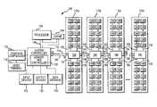
- FIG. 1is a block diagram of a processor-based system having system memory that uses a conventional memory hub architecture.
- FIG. 2is a block diagram of a processor-based system having system memory using a memory hub architecture according to one embodiment of the invention.
- a processor-based system 200is shown in FIG. 2 .
- the system 200uses most of the same components used in the system 100 of FIG. 1 , and they operate in the same manner. Therefore, in the interest of brevity, they have been provided with the same reference number, and an explanation of their operation will not be repeated.
- the processor-based system 200differs from the system 100 shown in FIG. 1 in that the widths of the downstream bus 154 and upstream bus 156 are not fixed, nor are they necessarily equal to each other. Instead, the downstream bus 154 has a width of M bits, and the upstream bus 156 has a width of N bits, where the sum of M and N is equal to a fixed value.
- the values of M and Nare dynamic, preferably depending on the nature of the actual or expected memory accesses. If a disproportionately large number of writes are occurring or expected to occur, the value of M is increased to increase the capacity of the downstream bus 154 , and the value of N is decreased accordingly to decrease the capacity of the upstream bus 156 . If a disproportionately large number of read are occurring or expected to occur, the value of M is decreased to decrease the capacity of the downstream bus 154 , and the value of N is increased accordingly to increase the capacity of the upstream bus 156 .
- the capacity M of the downstream bus 154 relative to the capacity N of the upstream bus 156can be determined using a variety of techniques.
- the system 200can be manually configured in a semi-permanent manner by manually manipulating hardware jumpers or the like to select the values of M and N.
- the values of M and Nmay be determined during system design based on the anticipated usage of the system 200 .
- the values of M and Nare preferably dynamic, i.e., they change during the operation of the system 200 .
- the values of M and Nmay be dynamically changed based on either the actual traffic flow through the buses 154 , 156 , or the anticipated traffic flow through the buses 154 , 156 .
- the values of M and Nmay be changed at other times during the operation of the memory system, such as when the memory system is being initialized.
- the traffic through the buses 154 , 156may be determined by the memory hub controller 128 and the memory hubs 140 , which can then adjust M and N by configuring internal buffers coupled to the signals lines in the buses 154 , 156 as either input buffers or output buffers.
- the traffic through the buses 154 , 156may be determined by only the memory hub controller 128 , which can couple configuration data to the memory hubs 140 . In such case, default values for M and N are used to couple the configuration to the memory hubs 140 .
- the memory hubs 140can then use the configuration data to configure internal buffers coupled to the signals lines in the buses 154 , 156 as either input buffers or output buffers.
- the actual traffic flowcould be determined by software, such as the operation system or run time agents. Other means of determining the actual traffic flow through the buses 154 , 156 can also be used.
- the anticipated traffic flowmay be determined by a user and then coupled to the memory hub controller 128 and the memory hubs 140 by suitable means.
- the anticipated usage informationcan be coupled through a suitable interface, such as a JTAG interface (not shown) or and 12 C interface (not shown).
- the memory hub controller 128 and the memory hubs 140can then configure internal buffers coupled to the signals lines in the buses 154 , 156 accordingly.
- the anticipated traffic flow through the buses 154 , 156may be either determined directly by a user, as explained above, or it may be inferred from other information.
- the anticipated traffic flow the buses 154 , 156may be determined based on either the type of hardware included in the system 200 or the software being executed by the processor 104 .
- the processor 104may determine the appropriate values of M and N and couple these values to the memory hub controller 128 and the memory hubs 140 based on the type of application program executed by the processor 104 . There are normally a large number of write accesses when an installation program is being executed. In such case, the processor 104 would increase the value of M and decrease the value of N.
- a graphics intensive application programnormally requires a disproportionate number of read accesses, so the value of M would be decreased and the value of N would be increased.
- a communications programnormally has about an equal number of reads and writes, so the value of M would be set equal to the value of N.
- Other hardware or software means for determining the expected traffic flow through the buses 154 , 156can alternatively be used.
- all of the signal lines in the buses 154 , 156may be configurable as bi-directional so that they can be either part of the downstream bus 154 or part of the upstream bus 156
- some of the lines in the buses 154 , 156 corresponding in number to minimum values of M and Nmay be uni-directional and thus dedicated to either the downstream bus 154 or the upstream bus 156 .
- the requirement that the input of an input buffer be coupled to each line that is also coupled to the output of an output buffermay have a tendency in some cases to overload the line.
- this potential problemcan be alleviated by equalization techniques or by decoupling the input buffers from the lines of the buses 154 , 156 when they are not in use, for example.
- the manner in which input and output buffers should be coupled to the buses 154 , 156 , as well as the specific hardware and software than can be used to determine the values of M and N,will be readily apparent to one skilled in the art.
Landscapes
- Engineering & Computer Science (AREA)
- Theoretical Computer Science (AREA)
- General Engineering & Computer Science (AREA)
- Physics & Mathematics (AREA)
- General Physics & Mathematics (AREA)
- Computer Hardware Design (AREA)
- Memory System (AREA)
- Bus Control (AREA)
- Information Transfer Systems (AREA)
- Multi Processors (AREA)
Abstract
Description
Claims (86)
Priority Applications (12)
| Application Number | Priority Date | Filing Date | Title |
|---|---|---|---|
| US10/797,727US7366864B2 (en) | 2004-03-08 | 2004-03-08 | Memory hub architecture having programmable lane widths |
| KR1020067020981AKR100872007B1 (en) | 2004-03-08 | 2005-03-04 | Memory hub architecture having programmable lane widths |
| CNA2005800075670ACN1930554A (en) | 2004-03-08 | 2005-03-04 | Memory Hub Architecture with Programmable Lane Width |
| EP05724531AEP1730640A4 (en) | 2004-03-08 | 2005-03-04 | Memory hub architecture having programmable lane widths |
| JP2007502867AJP2007528077A (en) | 2004-03-08 | 2005-03-04 | Memory hub architecture with programmable lane width |
| PCT/US2005/007007WO2005089126A2 (en) | 2004-03-08 | 2005-03-04 | Memory hub architecture having programmable lane widths |
| TW100101847ATW201120644A (en) | 2004-03-08 | 2005-03-08 | Memory hub architecture having programmable lane widths |
| TW094106980ATWI340897B (en) | 2004-03-08 | 2005-03-08 | Memory hub architecture having programmable lane widths |
| US12/074,888US7596675B2 (en) | 2004-03-08 | 2008-03-07 | Memory hub architecture having programmable lane widths |
| US12/550,989US8015384B2 (en) | 2004-03-08 | 2009-08-31 | Memory hub architecture having programmable lane widths |
| US13/208,198US8775764B2 (en) | 2004-03-08 | 2011-08-11 | Memory hub architecture having programmable lane widths |
| US14/300,903US9274991B2 (en) | 2004-03-08 | 2014-06-10 | Memory hub architecture having programmable lane widths |
Applications Claiming Priority (1)
| Application Number | Priority Date | Filing Date | Title |
|---|---|---|---|
| US10/797,727US7366864B2 (en) | 2004-03-08 | 2004-03-08 | Memory hub architecture having programmable lane widths |
Related Child Applications (1)
| Application Number | Title | Priority Date | Filing Date |
|---|---|---|---|
| US12/074,888ContinuationUS7596675B2 (en) | 2004-03-08 | 2008-03-07 | Memory hub architecture having programmable lane widths |
Publications (2)
| Publication Number | Publication Date |
|---|---|
| US20050210216A1 US20050210216A1 (en) | 2005-09-22 |
| US7366864B2true US7366864B2 (en) | 2008-04-29 |
Family
ID=34987711
Family Applications (5)
| Application Number | Title | Priority Date | Filing Date |
|---|---|---|---|
| US10/797,727Expired - LifetimeUS7366864B2 (en) | 2004-03-08 | 2004-03-08 | Memory hub architecture having programmable lane widths |
| US12/074,888Expired - LifetimeUS7596675B2 (en) | 2004-03-08 | 2008-03-07 | Memory hub architecture having programmable lane widths |
| US12/550,989Expired - LifetimeUS8015384B2 (en) | 2004-03-08 | 2009-08-31 | Memory hub architecture having programmable lane widths |
| US13/208,198Expired - LifetimeUS8775764B2 (en) | 2004-03-08 | 2011-08-11 | Memory hub architecture having programmable lane widths |
| US14/300,903Expired - LifetimeUS9274991B2 (en) | 2004-03-08 | 2014-06-10 | Memory hub architecture having programmable lane widths |
Family Applications After (4)
| Application Number | Title | Priority Date | Filing Date |
|---|---|---|---|
| US12/074,888Expired - LifetimeUS7596675B2 (en) | 2004-03-08 | 2008-03-07 | Memory hub architecture having programmable lane widths |
| US12/550,989Expired - LifetimeUS8015384B2 (en) | 2004-03-08 | 2009-08-31 | Memory hub architecture having programmable lane widths |
| US13/208,198Expired - LifetimeUS8775764B2 (en) | 2004-03-08 | 2011-08-11 | Memory hub architecture having programmable lane widths |
| US14/300,903Expired - LifetimeUS9274991B2 (en) | 2004-03-08 | 2014-06-10 | Memory hub architecture having programmable lane widths |
Country Status (7)
| Country | Link |
|---|---|
| US (5) | US7366864B2 (en) |
| EP (1) | EP1730640A4 (en) |
| JP (1) | JP2007528077A (en) |
| KR (1) | KR100872007B1 (en) |
| CN (1) | CN1930554A (en) |
| TW (2) | TWI340897B (en) |
| WO (1) | WO2005089126A2 (en) |
Cited By (2)
| Publication number | Priority date | Publication date | Assignee | Title |
|---|---|---|---|---|
| US20090006790A1 (en)* | 2007-06-27 | 2009-01-01 | Gerald Keith Bartley | High Capacity Memory Subsystem Architecture Storing Interleaved Data for Reduced Bus Speed |
| US20140310444A1 (en)* | 2013-04-12 | 2014-10-16 | Texas Instruments Incorporated | Dynamic balancing of bus bandwidth across multiple routes |
Families Citing this family (45)
| Publication number | Priority date | Publication date | Assignee | Title |
|---|---|---|---|---|
| US7200024B2 (en) | 2002-08-02 | 2007-04-03 | Micron Technology, Inc. | System and method for optically interconnecting memory devices |
| US7254331B2 (en) | 2002-08-09 | 2007-08-07 | Micron Technology, Inc. | System and method for multiple bit optical data transmission in memory systems |
| US7836252B2 (en) | 2002-08-29 | 2010-11-16 | Micron Technology, Inc. | System and method for optimizing interconnections of memory devices in a multichip module |
| DE112004000821B4 (en)* | 2003-05-13 | 2016-12-01 | Advanced Micro Devices, Inc. | System with a host connected to multiple storage modules via a serial storage connection |
| US7245145B2 (en) | 2003-06-11 | 2007-07-17 | Micron Technology, Inc. | Memory module and method having improved signal routing topology |
| US7133991B2 (en)* | 2003-08-20 | 2006-11-07 | Micron Technology, Inc. | Method and system for capturing and bypassing memory transactions in a hub-based memory system |
| US7120743B2 (en) | 2003-10-20 | 2006-10-10 | Micron Technology, Inc. | Arbitration system and method for memory responses in a hub-based memory system |
| US7234070B2 (en) | 2003-10-27 | 2007-06-19 | Micron Technology, Inc. | System and method for using a learning sequence to establish communications on a high-speed nonsynchronous interface in the absence of clock forwarding |
| US7181584B2 (en) | 2004-02-05 | 2007-02-20 | Micron Technology, Inc. | Dynamic command and/or address mirroring system and method for memory modules |
| US7366864B2 (en) | 2004-03-08 | 2008-04-29 | Micron Technology, Inc. | Memory hub architecture having programmable lane widths |
| US7120723B2 (en) | 2004-03-25 | 2006-10-10 | Micron Technology, Inc. | System and method for memory hub-based expansion bus |
| US7590797B2 (en) | 2004-04-08 | 2009-09-15 | Micron Technology, Inc. | System and method for optimizing interconnections of components in a multichip memory module |
| US7222213B2 (en) | 2004-05-17 | 2007-05-22 | Micron Technology, Inc. | System and method for communicating the synchronization status of memory modules during initialization of the memory modules |
| US7222224B2 (en)* | 2004-05-21 | 2007-05-22 | Rambus Inc. | System and method for improving performance in computer memory systems supporting multiple memory access latencies |
| US7392331B2 (en) | 2004-08-31 | 2008-06-24 | Micron Technology, Inc. | System and method for transmitting data packets in a computer system having a memory hub architecture |
| US9384818B2 (en) | 2005-04-21 | 2016-07-05 | Violin Memory | Memory power management |
| US7447831B2 (en)* | 2006-05-18 | 2008-11-04 | International Business Machines Corporation | Memory systems for automated computing machinery |
| US7490186B2 (en)* | 2006-07-26 | 2009-02-10 | International Business Machines Corporation | Memory system having an apportionable data bus and daisy chained memory chips |
| US7546410B2 (en)* | 2006-07-26 | 2009-06-09 | International Business Machines Corporation | Self timed memory chip having an apportionable data bus |
| US7844769B2 (en)* | 2006-07-26 | 2010-11-30 | International Business Machines Corporation | Computer system having an apportionable data bus and daisy chained memory chips |
| US7620763B2 (en)* | 2006-07-26 | 2009-11-17 | International Business Machines Corporation | Memory chip having an apportionable data bus |
| US7996641B2 (en)* | 2007-06-27 | 2011-08-09 | International Business Machines Corporation | Structure for hub for supporting high capacity memory subsystem |
| US7809913B2 (en)* | 2007-06-27 | 2010-10-05 | International Business Machines Corporation | Memory chip for high capacity memory subsystem supporting multiple speed bus |
| US8037258B2 (en)* | 2007-06-27 | 2011-10-11 | International Business Machines Corporation | Structure for dual-mode memory chip for high capacity memory subsystem |
| US7818512B2 (en)* | 2007-06-27 | 2010-10-19 | International Business Machines Corporation | High capacity memory subsystem architecture employing hierarchical tree configuration of memory modules |
| US8037272B2 (en)* | 2007-06-27 | 2011-10-11 | International Business Machines Corporation | Structure for memory chip for high capacity memory subsystem supporting multiple speed bus |
| US7822936B2 (en)* | 2007-06-27 | 2010-10-26 | International Business Machines Corporation | Memory chip for high capacity memory subsystem supporting replication of command data |
| US7921271B2 (en)* | 2007-06-27 | 2011-04-05 | International Business Machines Corporation | Hub for supporting high capacity memory subsystem |
| US20090006774A1 (en)* | 2007-06-27 | 2009-01-01 | Gerald Keith Bartley | High Capacity Memory Subsystem Architecture Employing Multiple-Speed Bus |
| US8037270B2 (en)* | 2007-06-27 | 2011-10-11 | International Business Machines Corporation | Structure for memory chip for high capacity memory subsystem supporting replication of command data |
| US7921264B2 (en)* | 2007-06-27 | 2011-04-05 | International Business Machines Corporation | Dual-mode memory chip for high capacity memory subsystem |
| WO2009110100A1 (en)* | 2008-03-03 | 2009-09-11 | Nec Corporation | A control apparatus for fast inter processing unit data exchange in a processor architecture with processing units of different bandwidth connection to a pipelined ring bus |
| US8656082B2 (en)* | 2008-08-05 | 2014-02-18 | Micron Technology, Inc. | Flexible and expandable memory architectures |
| US8412880B2 (en)* | 2009-01-08 | 2013-04-02 | Micron Technology, Inc. | Memory system controller to manage wear leveling across a plurality of storage nodes |
| US8463948B1 (en)* | 2011-07-01 | 2013-06-11 | Intel Corporation | Method, apparatus and system for determining an identifier of a volume of memory |
| WO2013048508A1 (en)* | 2011-09-30 | 2013-04-04 | Intel Corporation | Bandwidth configurable io connector |
| US8830716B2 (en)* | 2012-09-29 | 2014-09-09 | Intel Corporation | Intelligent far memory bandwith scaling |
| US9141541B2 (en) | 2013-09-20 | 2015-09-22 | Advanced Micro Devices, Inc. | Nested channel address interleaving |
| US10445025B2 (en)* | 2014-03-18 | 2019-10-15 | Micron Technology, Inc. | Apparatuses and methods having memory tier structure and recursively searching between tiers for address in a translation table where information is only directly transferred between controllers |
| CN104123249B (en)* | 2014-07-22 | 2018-03-09 | 山西达鑫核科技有限公司 | A kind of new dynamic memory SDDR architecture arrays of serial access |
| US10339072B2 (en)* | 2016-04-01 | 2019-07-02 | Intel Corporation | Read delivery for memory subsystem with narrow bandwidth repeater channel |
| JP7006166B2 (en)* | 2017-11-17 | 2022-01-24 | 富士通株式会社 | Data transfer device and data transfer method |
| US11262949B2 (en)* | 2020-05-28 | 2022-03-01 | Advanced Micro Devices, Inc. | Command throughput in PIM-enabled memory using available data bus bandwidth |
| US11726659B2 (en) | 2021-03-10 | 2023-08-15 | Samsung Electronics Co., Ltd. | Systems, methods, and devices for data storage with specified data transfer rate |
| TWI773517B (en)* | 2021-09-06 | 2022-08-01 | 宏正自動科技股份有限公司 | Hub control method |
Citations (165)
| Publication number | Priority date | Publication date | Assignee | Title |
|---|---|---|---|---|
| US3777154A (en) | 1972-02-07 | 1973-12-04 | R Lindsey | Optical data processing system |
| US4443845A (en)* | 1980-06-26 | 1984-04-17 | Texas Instruments Incorporated | Memory system having a common interface |
| US4813772A (en) | 1987-09-08 | 1989-03-21 | The Regents Of The University Of California | Electro-optical interface |
| US4823403A (en) | 1987-03-26 | 1989-04-18 | Switch Tech, Inc. | System for optically transmitting data between circuit packs, such as printed circuit boards |
| US4825208A (en) | 1986-04-23 | 1989-04-25 | Siemens Aktiengesellschaft | Method for flow control of data within a meshed data network |
| US4953930A (en) | 1989-03-15 | 1990-09-04 | Ramtech, Inc. | CPU socket supporting socket-to-socket optical communications |
| US5251303A (en) | 1989-01-13 | 1993-10-05 | International Business Machines Corporation | System for DMA block data transfer based on linked control blocks |
| US5307381A (en) | 1991-12-27 | 1994-04-26 | Intel Corporation | Skew-free clock signal distribution network in a microprocessor |
| US5327553A (en) | 1989-12-22 | 1994-07-05 | Tandem Computers Incorporated | Fault-tolerant computer system with /CONFIG filesystem |
| US5379382A (en) | 1991-04-22 | 1995-01-03 | Pilkington Micro-Electronics Limited | Uni and bi-directional signal transfer modes in peripheral controller and method of operating same |
| US5414819A (en) | 1992-12-18 | 1995-05-09 | Nec Research Institute, Inc. | Optical interconnection network |
| US5423009A (en)* | 1993-02-18 | 1995-06-06 | Sierra Semiconductor Corporation | Dynamic sizing bus controller that allows unrestricted byte enable patterns |
| US5432907A (en) | 1992-05-12 | 1995-07-11 | Network Resources Corporation | Network hub with integrated bridge |
| US5442770A (en) | 1989-01-24 | 1995-08-15 | Nec Electronics, Inc. | Triple port cache memory |
| GB2288066A (en) | 1994-03-31 | 1995-10-04 | Hewlett Packard Co | Integrated circuit having mirror-image pin assignments |
| US5465229A (en) | 1992-05-19 | 1995-11-07 | Sun Microsystems, Inc. | Single in-line memory module |
| US5493437A (en) | 1993-09-13 | 1996-02-20 | Motorola | External communication link for a credit card pager |
| US5497476A (en) | 1992-09-21 | 1996-03-05 | International Business Machines Corporation | Scatter-gather in data processing system |
| US5532856A (en) | 1994-06-30 | 1996-07-02 | Nec Research Institute, Inc. | Planar optical mesh-connected tree interconnect network |
| US5544319A (en) | 1992-03-25 | 1996-08-06 | Encore Computer U.S., Inc. | Fiber optic memory coupling system with converter transmitting and receiving bus data in parallel fashion and diagnostic data in serial fashion |
| US5544345A (en) | 1993-11-08 | 1996-08-06 | International Business Machines Corporation | Coherence controls for store-multiple shared data coordinated by cache directory entries in a shared electronic storage |
| US5568574A (en) | 1995-06-12 | 1996-10-22 | University Of Southern California | Modulator-based photonic chip-to-chip interconnections for dense three-dimensional multichip module integration |
| US5608264A (en) | 1995-06-05 | 1997-03-04 | Harris Corporation | Surface mountable integrated circuit with conductive vias |
| US5623534A (en) | 1995-04-07 | 1997-04-22 | Lucent Technologies Inc. | Method and apparatus for exchanging administrative information between local area networks |
| US5659798A (en) | 1996-02-02 | 1997-08-19 | Blumrich; Matthias Augustin | Method and system for initiating and loading DMA controller registers by using user-level programs |
| EP0849685A2 (en) | 1996-12-19 | 1998-06-24 | Texas Instruments Incorporated | Communication bus system between processors and memory modules |
| US5787475A (en)* | 1992-07-21 | 1998-07-28 | Digital Equipment Corporation | Controlled prefetching of data requested by a peripheral |
| US5818844A (en) | 1996-06-06 | 1998-10-06 | Advanced Micro Devices, Inc. | Address generation and data path arbitration to and from SRAM to accommodate multiple transmitted packets |
| US5818984A (en) | 1996-11-18 | 1998-10-06 | International Business Machines Corporation | Optoelectronic interconnection of integrated circuits |
| US5822255A (en) | 1996-08-13 | 1998-10-13 | Fujitsu Limited | Semiconductor integrated circuit for supplying a control signal to a plurality of object circuits |
| US5831467A (en) | 1991-11-05 | 1998-11-03 | Monolithic System Technology, Inc. | Termination circuit with power-down mode for use in circuit module architecture |
| US5875352A (en) | 1995-11-03 | 1999-02-23 | Sun Microsystems, Inc. | Method and apparatus for multiple channel direct memory access control |
| US5875454A (en) | 1996-07-24 | 1999-02-23 | International Business Machiness Corporation | Compressed data cache storage system |
| US5987196A (en) | 1997-11-06 | 1999-11-16 | Micron Technology, Inc. | Semiconductor structure having an optical signal path in a substrate and method for forming the same |
| US6026226A (en)* | 1996-10-28 | 2000-02-15 | Altera Corporation | Local compilation in context within a design hierarchy |
| US6033951A (en) | 1996-08-16 | 2000-03-07 | United Microelectronics Corp. | Process for fabricating a storage capacitor for semiconductor memory devices |
| US6061263A (en) | 1998-12-29 | 2000-05-09 | Intel Corporation | Small outline rambus in-line memory module |
| US6067262A (en) | 1998-12-11 | 2000-05-23 | Lsi Logic Corporation | Redundancy analysis for embedded memories with built-in self test and built-in self repair |
| US6073190A (en)* | 1997-07-18 | 2000-06-06 | Micron Electronics, Inc. | System for dynamic buffer allocation comprising control logic for controlling a first address buffer and a first data buffer as a matched pair |
| US6078451A (en) | 1996-09-17 | 2000-06-20 | International Business Machines Corporation | Method and apparatus for adjusting data window phase when retrieving data stored on a recording medium |
| US6079008A (en) | 1998-04-03 | 2000-06-20 | Patton Electronics Co. | Multiple thread multiple data predictive coded parallel processing system and method |
| US6088774A (en) | 1996-09-20 | 2000-07-11 | Advanced Memory International, Inc. | Read/write timing for maximum utilization of bidirectional read/write bus |
| US6101151A (en) | 1998-06-12 | 2000-08-08 | Mitsubishi Denki Kabushiki Kaisha | Synchronous semiconductor memory device employing temporary data output stop scheme |
| US6105075A (en) | 1997-08-05 | 2000-08-15 | Adaptec, Inc. | Scatter gather memory system for a hardware accelerated command interpreter engine |
| US6105088A (en) | 1998-07-10 | 2000-08-15 | Northrop Grumman Corporation | Backplane assembly for electronic circuit modules providing electronic reconfigurable connectivity of digital signals and manual reconfigurable connectivity power, optical and RF signals |
| US6111757A (en) | 1998-01-16 | 2000-08-29 | International Business Machines Corp. | SIMM/DIMM memory module |
| US6131149A (en) | 1997-06-04 | 2000-10-10 | Oak Technology, Inc. | Apparatus and method for reading data from synchronous memory with skewed clock pulses |
| US6144327A (en) | 1996-08-15 | 2000-11-07 | Intellectual Property Development Associates Of Connecticut, Inc. | Programmably interconnected programmable devices |
| US6144587A (en) | 1998-06-23 | 2000-11-07 | Nec Corporation | Semiconductor memory device |
| US6167486A (en) | 1996-11-18 | 2000-12-26 | Nec Electronics, Inc. | Parallel access virtual channel memory system with cacheable channels |
| US6167465A (en) | 1998-05-20 | 2000-12-26 | Aureal Semiconductor, Inc. | System for managing multiple DMA connections between a peripheral device and a memory and performing real-time operations on data carried by a selected DMA connection |
| US6186400B1 (en) | 1998-03-20 | 2001-02-13 | Symbol Technologies, Inc. | Bar code reader with an integrated scanning component module mountable on printed circuit board |
| US6201724B1 (en) | 1998-11-12 | 2001-03-13 | Nec Corporation | Semiconductor memory having improved register array access speed |
| US6226729B1 (en) | 1998-11-03 | 2001-05-01 | Intel Corporation | Method and apparatus for configuring and initializing a memory device and a memory channel |
| US6229727B1 (en) | 1998-09-28 | 2001-05-08 | Cisco Technology, Inc. | Method and apparatus for support of multiple memory devices in a single memory socket architecture |
| US6229712B1 (en) | 1999-03-31 | 2001-05-08 | International Business Machines Corporation | Printed circuit board for coupling surface mounted optoelectric semiconductor devices |
| US6233376B1 (en) | 1999-05-18 | 2001-05-15 | The United States Of America As Represented By The Secretary Of The Navy | Embedded fiber optic circuit boards and integrated circuits |
| US6243769B1 (en) | 1997-07-18 | 2001-06-05 | Micron Technology, Inc. | Dynamic buffer allocation for a computer system |
| US6243831B1 (en) | 1998-10-31 | 2001-06-05 | Compaq Computer Corporation | Computer system with power loss protection mechanism |
| US6246618B1 (en) | 2000-06-30 | 2001-06-12 | Mitsubishi Denki Kabushiki Kaisha | Semiconductor integrated circuit capable of testing and substituting defective memories and method thereof |
| US6256253B1 (en) | 2000-02-18 | 2001-07-03 | Infineon Technologies North America Corp. | Memory device with support for unaligned access |
| US6256692B1 (en) | 1997-10-13 | 2001-07-03 | Fujitsu Limited | CardBus interface circuit, and a CardBus PC having the same |
| US6266730B1 (en) | 1997-09-26 | 2001-07-24 | Rambus Inc. | High-frequency bus system |
| US6272609B1 (en) | 1998-07-31 | 2001-08-07 | Micron Electronics, Inc. | Pipelined memory controller |
| US6285349B1 (en) | 1999-02-26 | 2001-09-04 | Intel Corporation | Correcting non-uniformity in displays |
| US20010023474A1 (en) | 2000-03-16 | 2001-09-20 | Fuji Xerox Co., Ltd | Array storage device and information processing system |
| US6301637B1 (en)* | 1998-06-08 | 2001-10-09 | Storage Technology Corporation | High performance data paths |
| US20010034839A1 (en) | 1999-12-24 | 2001-10-25 | Guenter Karjoth | Method and apparatus for secure transmission of data and applications |
| US6330205B2 (en) | 1999-12-22 | 2001-12-11 | Nec Corporation | Virtual channel synchronous dynamic random access memory |
| US6343171B1 (en) | 1998-10-09 | 2002-01-29 | Fujitsu Limited | Systems based on opto-electronic substrates with electrical and optical interconnections and methods for making |
| US6344664B1 (en) | 1999-12-02 | 2002-02-05 | Tera Connect Inc. | Electro-optical transceiver system with controlled lateral leakage and method of making it |
| US6347055B1 (en) | 1999-06-24 | 2002-02-12 | Nec Corporation | Line buffer type semiconductor memory device capable of direct prefetch and restore operations |
| US6349363B2 (en) | 1998-12-08 | 2002-02-19 | Intel Corporation | Multi-section cache with different attributes for each section |
| US6356573B1 (en) | 1998-01-31 | 2002-03-12 | Mitel Semiconductor Ab | Vertical cavity surface emitting laser |
| US20020038412A1 (en) | 1998-11-03 | 2002-03-28 | Nizar Puthiya K. | Method and apparatus for configuring a memory device and a memory channel using configuration space registers |
| US6367074B1 (en) | 1998-12-28 | 2002-04-02 | Intel Corporation | Operation of a system |
| US6366375B1 (en) | 1997-11-10 | 2002-04-02 | Fuji Xerox Co., Ltd. | Optical-signal transmission apparatus and method, and signal processing apparatus |
| US6373777B1 (en)* | 1998-07-14 | 2002-04-16 | Nec Corporation | Semiconductor memory |
| US6381190B1 (en) | 1999-05-13 | 2002-04-30 | Nec Corporation | Semiconductor memory device in which use of cache can be selected |
| US6392653B1 (en) | 1998-06-25 | 2002-05-21 | Inria Institut National De Recherche En Informatique Et En Automatique | Device for processing acquisition data, in particular image data |
| US6405273B1 (en) | 1998-11-13 | 2002-06-11 | Infineon Technologies North America Corp. | Data processing device with memory coupling unit |
| US6421744B1 (en) | 1999-10-25 | 2002-07-16 | Motorola, Inc. | Direct memory access controller and method therefor |
| US6434639B1 (en) | 1998-11-13 | 2002-08-13 | Intel Corporation | System for combining requests associated with one or more memory locations that are collectively associated with a single cache line to furnish a single memory operation |
| US6434654B1 (en)* | 1999-03-26 | 2002-08-13 | Koninklijke Philips Electronics N.V. | System bus with a variable width selectivity configurable at initialization |
| US20020112119A1 (en) | 1998-02-13 | 2002-08-15 | Intel Corporation | Dual-port buffer-to-memory interface |
| US6438668B1 (en) | 1999-09-30 | 2002-08-20 | Apple Computer, Inc. | Method and apparatus for reducing power consumption in a digital processing system |
| US6453377B1 (en) | 1998-06-16 | 2002-09-17 | Micron Technology, Inc. | Computer including optical interconnect, memory unit, and method of assembling a computer |
| US6457116B1 (en) | 1997-10-31 | 2002-09-24 | Broadcom Corporation | Method and apparatus for controlling contexts of multiple context processing elements in a network of multiple context processing elements |
| US20020144064A1 (en) | 2001-03-30 | 2002-10-03 | Fanning Blaise B. | Controlling cache memory in external chipset using processor |
| US6462978B2 (en) | 1997-08-21 | 2002-10-08 | Hitachi, Ltd. | Method of designing semiconductor integrated circuit device and semiconductor integrated circuit device |
| US6463059B1 (en) | 1998-12-04 | 2002-10-08 | Koninklijke Philips Electronics N.V. | Direct memory access execution engine with indirect addressing of circular queues in addition to direct memory addressing |
| US6473828B1 (en) | 1998-07-03 | 2002-10-29 | Nec Corporation | Virtual channel synchronous dynamic random access memory |
| US6477614B1 (en)* | 1998-09-30 | 2002-11-05 | Intel Corporation | Method for implementing multiple memory buses on a memory module |
| US6477592B1 (en) | 1999-08-06 | 2002-11-05 | Integrated Memory Logic, Inc. | System for I/O interfacing for semiconductor chip utilizing addition of reference element to each data element in first data stream and interpret to recover data elements of second data stream |
| US6493784B1 (en) | 1998-12-25 | 2002-12-10 | Fuji Xerox Co., Ltd. | Communication device, multiple bus control device and LSI for controlling multiple bus |
| US6496909B1 (en) | 1999-04-06 | 2002-12-17 | Silicon Graphics, Inc. | Method for managing concurrent access to virtual memory data structures |
| US6502161B1 (en) | 2000-01-05 | 2002-12-31 | Rambus Inc. | Memory system including a point-to-point linked memory subsystem |
| US20030005223A1 (en) | 2001-06-27 | 2003-01-02 | Coulson Richard L. | System boot time reduction method |
| US6505287B2 (en) | 1999-12-20 | 2003-01-07 | Nec Corporation | Virtual channel memory access controlling circuit |
| US6507899B1 (en) | 1999-12-13 | 2003-01-14 | Infineon Technologies North American Corp. | Interface for a memory unit |
| US6523092B1 (en) | 2000-09-29 | 2003-02-18 | Intel Corporation | Cache line replacement policy enhancement to avoid memory page thrashing |
| US6523093B1 (en) | 2000-09-29 | 2003-02-18 | Intel Corporation | Prefetch buffer allocation and filtering system |
| US6526498B1 (en) | 1997-10-31 | 2003-02-25 | Broadcom Corporation | Method and apparatus for retiming in a network of multiple context processing elements |
| US20030043426A1 (en) | 2001-08-30 | 2003-03-06 | Baker R. J. | Optical interconnect in high-speed memory systems |
| US6539490B1 (en) | 1999-08-30 | 2003-03-25 | Micron Technology, Inc. | Clock distribution without clock delay or skew |
| US6552304B1 (en) | 1998-05-20 | 2003-04-22 | Fujitsu Limited | Temperature control method and system for thermal fixing unit, and image forming apparatus |
| US6552564B1 (en) | 1999-08-30 | 2003-04-22 | Micron Technology, Inc. | Technique to reduce reflections and ringing on CMOS interconnections |
| US6567963B1 (en) | 1999-10-22 | 2003-05-20 | Tera Connect, Inc. | Wafer scale integration and remoted subsystems using opto-electronic transceivers |
| US6570429B1 (en) | 2000-10-20 | 2003-05-27 | Cray Inc. | Method and apparatus for providing a clock signal to a semiconductor chip |
| US6584543B2 (en) | 1999-07-22 | 2003-06-24 | Micron Technology, Inc. | Reconfigurable memory with selectable error correction storage |
| US6590816B2 (en) | 2001-03-05 | 2003-07-08 | Infineon Technologies Ag | Integrated memory and method for testing and repairing the integrated memory |
| US6594713B1 (en)* | 1999-09-10 | 2003-07-15 | Texas Instruments Incorporated | Hub interface unit and application unit interfaces for expanded direct memory access processor |
| US6599031B2 (en) | 2001-09-12 | 2003-07-29 | Intel Corporation | Optical/electrical interconnects and package for high speed signaling |
| US6622227B2 (en) | 2000-12-27 | 2003-09-16 | Intel Corporation | Method and apparatus for utilizing write buffers in memory control/interface |
| US6631440B2 (en) | 2000-11-30 | 2003-10-07 | Hewlett-Packard Development Company | Method and apparatus for scheduling memory calibrations based on transactions |
| US6636110B1 (en) | 1998-05-01 | 2003-10-21 | Mitsubishi Denki Kabushiki Kaisha | Internal clock generating circuit for clock synchronous semiconductor memory device |
| US6651139B1 (en) | 1999-03-15 | 2003-11-18 | Fuji Xerox Co., Ltd. | Multiprocessor system |
| US6661943B2 (en) | 2002-01-30 | 2003-12-09 | Intel Corporation | Fiber-free optical interconnect system for chip-to-chip signaling |
| US6661940B2 (en) | 2000-07-21 | 2003-12-09 | Finisar Corporation | Apparatus and method for rebroadcasting signals in an optical backplane bus system |
| US20030229770A1 (en) | 2002-06-07 | 2003-12-11 | Jeddeloh Joseph M. | Memory hub with internal cache and/or memory access prediction |
| US20030229734A1 (en) | 2002-06-05 | 2003-12-11 | Lsi Logic Corporation | FIFO scheduling time sharing |
| US6667895B2 (en) | 2001-12-06 | 2003-12-23 | Samsung Electronics Co., Ltd. | Integrated circuit device and module with integrated circuits |
| US6681292B2 (en) | 2001-08-27 | 2004-01-20 | Intel Corporation | Distributed read and write caching implementation for optimized input/output applications |
| US20040044833A1 (en) | 2002-08-29 | 2004-03-04 | Ryan Kevin J. | System and method for optimizing interconnections of memory devices in a multichip module |
| US6707726B2 (en) | 2001-07-30 | 2004-03-16 | Elpida Memory, Inc. | Register without restriction of number of mounted memory devices and memory module having the same |
| US6721187B2 (en) | 2001-03-16 | 2004-04-13 | International Business Machines Corporation | Multi-layered high density connections |
| US6751113B2 (en) | 2002-03-07 | 2004-06-15 | Netlist, Inc. | Arrangement of integrated circuits in a memory module |
| US6752539B2 (en) | 2002-06-28 | 2004-06-22 | International Buisness Machines Corporation | Apparatus and system for providing optical bus interprocessor interconnection |
| US6754117B2 (en) | 2002-08-16 | 2004-06-22 | Micron Technology, Inc. | System and method for self-testing and repair of memory modules |
| US20040123088A1 (en) | 2002-12-19 | 2004-06-24 | Poisner David I. | Method and apparatus for detecting an interruption in memory initialization |
| US20040128421A1 (en) | 2002-12-30 | 2004-07-01 | Intel Corporation | Apparatus and method for providing upgraded system memory for mobile platforms using mobile docking stations |
| US20040126115A1 (en) | 2002-12-31 | 2004-07-01 | Levy Paul S. | System having multiple agents on optical and electrical bus |
| US20040144994A1 (en) | 2003-01-23 | 2004-07-29 | Lee Terry R. | Apparatus and methods for optically-coupled memory systems |
| US20040148482A1 (en) | 2003-01-13 | 2004-07-29 | Grundy Kevin P. | Memory chain |
| US6772261B1 (en) | 2000-04-27 | 2004-08-03 | International Business Machines Corporation | Interface that allows testing and using memory modules in computer systems not designed for the modules |
| US6793408B2 (en) | 2002-12-31 | 2004-09-21 | Intel Corporation | Module interface with optical and electrical interconnects |
| US6793411B2 (en) | 2000-12-22 | 2004-09-21 | Nufern | Method and apparatus for communicating signals with an optical fiber |
| US6811320B1 (en) | 2002-11-13 | 2004-11-02 | Russell Mistretta Abbott | System for connecting a fiber optic cable to an electronic device |
| US6816931B2 (en) | 2002-04-10 | 2004-11-09 | Avision Inc. | Upstream peripheral device serving as a USB host |
| US20040230718A1 (en) | 2003-05-13 | 2004-11-18 | Advanced Micro Devices, Inc. | System including a host connected to a plurality of memory modules via a serial memory interconnet |
| US6821029B1 (en) | 2002-09-10 | 2004-11-23 | Xilinx, Inc. | High speed serial I/O technology using an optical link |
| US20040257890A1 (en) | 2002-09-09 | 2004-12-23 | Lee Terry R. | Wavelength division multiplexed memory module, memory system and method |
| US20040268009A1 (en) | 2003-06-11 | 2004-12-30 | Samsung Electronics Co., Ltd. | Transceiving network controller and method for controlling buffer memory allocation and data flow |
| US20050105350A1 (en) | 2003-11-13 | 2005-05-19 | David Zimmerman | Memory channel test fixture and method |
| US6910812B2 (en) | 2001-05-15 | 2005-06-28 | Peregrine Semiconductor Corporation | Small-scale optoelectronic package |
| US20050177690A1 (en) | 2004-02-05 | 2005-08-11 | Laberge Paul A. | Dynamic command and/or address mirroring system and method for memory modules |
| US20050210185A1 (en) | 2004-03-18 | 2005-09-22 | Kirsten Renick | System and method for organizing data transfers with memory hub memory modules |
| US6950956B2 (en) | 1999-10-19 | 2005-09-27 | Rambus Inc. | Integrated circuit with timing adjustment mechanism and method |
| US6949406B2 (en) | 2003-04-24 | 2005-09-27 | Sun Microsystems, Inc. | Method and apparatus for optically aligning integrated circuit devices |
| US20050216648A1 (en) | 2004-03-25 | 2005-09-29 | Jeddeloh Joseph M | System and method for memory hub-based expansion bus |
| US6956996B2 (en) | 2002-04-24 | 2005-10-18 | Agilent Technologies, Inc. | Tri-state optical systems and methods |
| US20050257021A1 (en) | 2004-05-17 | 2005-11-17 | Ralph James | System and method for communicating the synchronization status of memory modules during initialization of the memory modules |
| US20050268060A1 (en) | 2004-05-28 | 2005-12-01 | Cronin Jeffrey J | Method and system for terminating write commands in a hub-based memory system |
| US6980748B2 (en) | 2001-08-30 | 2005-12-27 | International Business Machines Corporation | SiGe or germanium flip chip optical receiver |
| US6982892B2 (en) | 2003-05-08 | 2006-01-03 | Micron Technology, Inc. | Apparatus and methods for a physical layout of simultaneously sub-accessible memory modules |
| US7000062B2 (en) | 2000-01-05 | 2006-02-14 | Rambus Inc. | System and method featuring a controller device and a memory module that includes an integrated circuit buffer device and a plurality of integrated circuit memory devices |
| US20060047891A1 (en) | 2004-08-31 | 2006-03-02 | Ralph James | System and method for transmitting data packets in a computer system having a memory hub architecture |
| US7016606B2 (en) | 2000-02-28 | 2006-03-21 | University Of Maryland Baltimore County | Error mitigation system using line coding for optical WDM communications |
| US7024547B2 (en) | 2001-12-10 | 2006-04-04 | Intel Corporation | Method and system for initializing a hardware device |
| US7035212B1 (en) | 2001-01-25 | 2006-04-25 | Optim Networks | Method and apparatus for end to end forwarding architecture |
| US7047351B2 (en) | 2002-08-16 | 2006-05-16 | Micron Technology, Inc. | Memory hub bypass circuit and method |
| US7062595B2 (en) | 2001-04-24 | 2006-06-13 | Broadcom Corporation | Integrated gigabit ethernet PCI-X controller |
| US7106973B2 (en) | 2002-08-13 | 2006-09-12 | Lightpointe Communications, Inc. | Apparatus and method for use in free-space optical communication comprising optically aligned components integrated on circuit boards |
| US7136953B1 (en)* | 2003-05-07 | 2006-11-14 | Nvidia Corporation | Apparatus, system, and method for bus link width optimization |
| US7171508B2 (en)* | 2004-08-23 | 2007-01-30 | Micron Technology, Inc. | Dual port memory with asymmetric inputs and outputs, device, system and method |
Family Cites Families (167)
| Publication number | Priority date | Publication date | Assignee | Title |
|---|---|---|---|---|
| US444384A (en)* | 1891-01-06 | Tennis-court marker | ||
| US630163A (en)* | 1898-08-17 | 1899-08-01 | Charles C Ball | Heater. |
| US4045781A (en) | 1976-02-13 | 1977-08-30 | Digital Equipment Corporation | Memory module with selectable byte addressing for digital data processing system |
| US4253144A (en) | 1978-12-21 | 1981-02-24 | Burroughs Corporation | Multi-processor communication network |
| US4253146A (en) | 1978-12-21 | 1981-02-24 | Burroughs Corporation | Module for coupling computer-processors |
| US4245306A (en) | 1978-12-21 | 1981-01-13 | Burroughs Corporation | Selection of addressed processor in a multi-processor network |
| US4240143A (en) | 1978-12-22 | 1980-12-16 | Burroughs Corporation | Hierarchical multi-processor network for memory sharing |
| KR900007564B1 (en)* | 1984-06-26 | 1990-10-15 | 모토로라 인코포레이티드 | Data processor with a dynamic bus |
| US4608702A (en) | 1984-12-21 | 1986-08-26 | Advanced Micro Devices, Inc. | Method for digital clock recovery from Manchester-encoded signals |
| US4724520A (en) | 1985-07-01 | 1988-02-09 | United Technologies Corporation | Modular multiport data hub |
| US4707823A (en) | 1986-07-21 | 1987-11-17 | Chrysler Motors Corporation | Fiber optic multiplexed data acquisition system |
| US4809232A (en) | 1986-12-16 | 1989-02-28 | The United States Of America As Represented By The United States Department Of Energy | High speed, very large (8 megabyte) first in/first out buffer memory (FIFO) |
| JPH07117863B2 (en) | 1987-06-26 | 1995-12-18 | 株式会社日立製作所 | Online system restart method |
| US4891808A (en) | 1987-12-24 | 1990-01-02 | Coherent Communication Systems Corp. | Self-synchronizing multiplexer |
| US5125084A (en)* | 1988-05-26 | 1992-06-23 | Ibm Corporation | Control of pipelined operation in a microcomputer system employing dynamic bus sizing with 80386 processor and 82385 cache controller |
| JPH0359753A (en)* | 1989-07-28 | 1991-03-14 | Seiko Epson Corp | bidirectional bus buffer |
| JPH03156795A (en) | 1989-11-15 | 1991-07-04 | Toshiba Micro Electron Kk | Semiconductor memory circuit device |
| US5317752A (en) | 1989-12-22 | 1994-05-31 | Tandem Computers Incorporated | Fault-tolerant computer system with auto-restart after power-fall |
| JP2772103B2 (en) | 1990-03-28 | 1998-07-02 | 株式会社東芝 | Computer system startup method |
| US5243703A (en) | 1990-04-18 | 1993-09-07 | Rambus, Inc. | Apparatus for synchronously generating clock signals in a data processing system |
| IL96808A (en) | 1990-04-18 | 1996-03-31 | Rambus Inc | Integrated circuit i/o using a high performance bus interface |
| JP2836321B2 (en)* | 1991-11-05 | 1998-12-14 | 三菱電機株式会社 | Data processing device |
| US5461627A (en) | 1991-12-24 | 1995-10-24 | Rypinski; Chandos A. | Access protocol for a common channel wireless network |
| JP2554816B2 (en) | 1992-02-20 | 1996-11-20 | 株式会社東芝 | Semiconductor memory device |
| DE4345604B3 (en) | 1992-03-06 | 2012-07-12 | Rambus Inc. | Device for communication with a DRAM |
| US5355391A (en) | 1992-03-06 | 1994-10-11 | Rambus, Inc. | High speed bus system |
| US5369550A (en) | 1992-09-02 | 1994-11-29 | Vlsi Technology, Inc. | Method and apparatus for cooling a molded-plastic integrated-circuit package |
| JP3369227B2 (en)* | 1992-11-09 | 2003-01-20 | 株式会社東芝 | Processor |
| JP3608804B2 (en)* | 1993-05-14 | 2005-01-12 | 株式会社ソニー・コンピュータエンタテインメント | Bus control device |
| JPH0713945A (en) | 1993-06-16 | 1995-01-17 | Nippon Sheet Glass Co Ltd | Bus structure of multiprocessor system with separated arithmetic processing part and control/storage part |
| US5829007A (en) | 1993-06-24 | 1998-10-27 | Discovision Associates | Technique for implementing a swing buffer in a memory array |
| US5497494A (en) | 1993-07-23 | 1996-03-05 | International Business Machines Corporation | Method for saving and restoring the state of a CPU executing code in protected mode |
| US5729709A (en) | 1993-11-12 | 1998-03-17 | Intel Corporation | Memory controller with burst addressing circuit |
| US5566325A (en) | 1994-06-30 | 1996-10-15 | Digital Equipment Corporation | Method and apparatus for adaptive memory access |
| US6175571B1 (en) | 1994-07-22 | 2001-01-16 | Network Peripherals, Inc. | Distributed memory switching hub |
| US5978567A (en) | 1994-07-27 | 1999-11-02 | Instant Video Technologies Inc. | System for distribution of interactive multimedia and linear programs by enabling program webs which include control scripts to define presentation by client transceiver |
| US5553070A (en) | 1994-09-13 | 1996-09-03 | Riley; Robert E. | Data link module for time division multiplexing control systems |
| US6804760B2 (en) | 1994-12-23 | 2004-10-12 | Micron Technology, Inc. | Method for determining a type of memory present in a system |
| US5715456A (en) | 1995-02-13 | 1998-02-03 | International Business Machines Corporation | Method and apparatus for booting a computer system without pre-installing an operating system |
| US5834956A (en) | 1995-12-29 | 1998-11-10 | Intel Corporation | Core clock correction in a 2/N mode clocking scheme |
| US5966724A (en) | 1996-01-11 | 1999-10-12 | Micron Technology, Inc. | Synchronous memory device with dual page and burst mode operations |
| US7681005B1 (en) | 1996-01-11 | 2010-03-16 | Micron Technology, Inc. | Asynchronously-accessible memory device with mode selection circuitry for burst or pipelined operation |
| US5832250A (en) | 1996-01-26 | 1998-11-03 | Unisys Corporation | Multi set cache structure having parity RAMs holding parity bits for tag data and for status data utilizing prediction circuitry that predicts and generates the needed parity bits |
| US5819304A (en) | 1996-01-29 | 1998-10-06 | Iowa State University Research Foundation, Inc. | Random access memory assembly |
| US5808897A (en) | 1996-03-05 | 1998-09-15 | Micron Technology, Inc. | Integrated circuit device having interchangeable terminal connection |
| JPH09319693A (en)* | 1996-05-28 | 1997-12-12 | Hitachi Ltd | Data transfer device and parallel computer system |
| JPH1049511A (en) | 1996-08-02 | 1998-02-20 | Oki Electric Ind Co Ltd | One-chip micrcomputer |
| DE19636381C1 (en)* | 1996-09-09 | 1998-03-12 | Ibm | Processor bus for bi-directional data transfer |
| US5706224A (en) | 1996-10-10 | 1998-01-06 | Quality Semiconductor, Inc. | Content addressable memory and random access memory partition circuit |
| US6308248B1 (en) | 1996-12-31 | 2001-10-23 | Compaq Computer Corporation | Method and system for allocating memory space using mapping controller, page table and frame numbers |
| US6031241A (en) | 1997-03-11 | 2000-02-29 | University Of Central Florida | Capillary discharge extreme ultraviolet lamp source for EUV microlithography and other related applications |
| JPH10262020A (en) | 1997-03-18 | 1998-09-29 | Fujitsu Ltd | Line multiplexing method |
| US6271582B1 (en) | 1997-04-07 | 2001-08-07 | Micron Technology, Inc. | Interdigitated leads-over-chip lead frame, device, and method for supporting an integrated circuit die |
| US6760833B1 (en) | 1997-08-01 | 2004-07-06 | Micron Technology, Inc. | Split embedded DRAM processor |
| US6249802B1 (en) | 1997-09-19 | 2001-06-19 | Silicon Graphics, Inc. | Method, system, and computer program product for allocating physical memory in a distributed shared memory network |
| US6098158A (en) | 1997-12-18 | 2000-08-01 | International Business Machines Corporation | Software-enabled fast boot |
| US6023726A (en) | 1998-01-20 | 2000-02-08 | Netscape Communications Corporation | User configurable prefetch control system for enabling client to prefetch documents from a network server |
| US6247107B1 (en) | 1998-04-06 | 2001-06-12 | Advanced Micro Devices, Inc. | Chipset configured to perform data-directed prefetching |
| US6084688A (en)* | 1998-04-30 | 2000-07-04 | Xerox Corporation | Network print server with page-parallel decomposing |
| KR100283243B1 (en) | 1998-05-11 | 2001-03-02 | 구자홍 | How to boot the operating system |
| SG75958A1 (en) | 1998-06-01 | 2000-10-24 | Hitachi Ulsi Sys Co Ltd | Semiconductor device and a method of producing semiconductor device |
| US6405280B1 (en) | 1998-06-05 | 2002-06-11 | Micron Technology, Inc. | Packet-oriented synchronous DRAM interface supporting a plurality of orderings for data block transfers within a burst sequence |
| US6134624A (en) | 1998-06-08 | 2000-10-17 | Storage Technology Corporation | High bandwidth cache system |
| US6286083B1 (en) | 1998-07-08 | 2001-09-04 | Compaq Computer Corporation | Computer system with adaptive memory arbitration scheme |
| US6912637B1 (en) | 1998-07-08 | 2005-06-28 | Broadcom Corporation | Apparatus and method for managing memory in a network switch |
| US6061296A (en) | 1998-08-17 | 2000-05-09 | Vanguard International Semiconductor Corporation | Multiple data clock activation with programmable delay for use in multiple CAS latency memory devices |
| US6219725B1 (en) | 1998-08-28 | 2001-04-17 | Hewlett-Packard Company | Method and apparatus for performing direct memory access transfers involving non-sequentially-addressable memory locations |
| US6029250A (en) | 1998-09-09 | 2000-02-22 | Micron Technology, Inc. | Method and apparatus for adaptively adjusting the timing offset between a clock signal and digital signals transmitted coincident with that clock signal, and memory device and system using same |
| US6910109B2 (en) | 1998-09-30 | 2005-06-21 | Intel Corporation | Tracking memory page state |
| US6438622B1 (en) | 1998-11-17 | 2002-08-20 | Intel Corporation | Multiprocessor system including a docking system |
| US6430696B1 (en) | 1998-11-30 | 2002-08-06 | Micron Technology, Inc. | Method and apparatus for high speed data capture utilizing bit-to-bit timing correction, and memory device using same |
| US6374360B1 (en) | 1998-12-11 | 2002-04-16 | Micron Technology, Inc. | Method and apparatus for bit-to-bit timing correction of a high speed memory bus |
| US6191663B1 (en) | 1998-12-22 | 2001-02-20 | Intel Corporation | Echo reduction on bit-serial, multi-drop bus |
| US6598154B1 (en) | 1998-12-29 | 2003-07-22 | Intel Corporation | Precoding branch instructions to reduce branch-penalty in pipelined processors |
| US6618777B1 (en)* | 1999-01-21 | 2003-09-09 | Analog Devices, Inc. | Method and apparatus for communicating between multiple functional units in a computer environment |
| AU3073800A (en) | 1999-02-01 | 2000-08-25 | Hitachi Limited | Semiconductor integrated circuit and nonvolatile memory element |
| US6564329B1 (en) | 1999-03-16 | 2003-05-13 | Linkup Systems Corporation | System and method for dynamic clock generation |
| US6294937B1 (en) | 1999-05-25 | 2001-09-25 | Lsi Logic Corporation | Method and apparatus for self correcting parallel I/O circuitry |
| US6449308B1 (en) | 1999-05-25 | 2002-09-10 | Intel Corporation | High-speed digital distribution system |
| JP3721283B2 (en) | 1999-06-03 | 2005-11-30 | 株式会社日立製作所 | Main memory shared multiprocessor system |
| US6826160B1 (en)* | 1999-07-07 | 2004-11-30 | 3Com Corporation | Dynamic bandwidth allocation through multi-channel time slot assignment and migration for broadband access |
| US6434736B1 (en) | 1999-07-08 | 2002-08-13 | Intel Corporation | Location based timing scheme in memory design |
| US6401213B1 (en) | 1999-07-09 | 2002-06-04 | Micron Technology, Inc. | Timing circuit for high speed memory |
| US7827348B2 (en) | 2000-01-06 | 2010-11-02 | Super Talent Electronics, Inc. | High performance flash memory devices (FMD) |
| US6629220B1 (en) | 1999-08-20 | 2003-09-30 | Intel Corporation | Method and apparatus for dynamic arbitration between a first queue and a second queue based on a high priority transaction type |
| US6493803B1 (en) | 1999-08-23 | 2002-12-10 | Advanced Micro Devices, Inc. | Direct memory access controller with channel width configurability support |
| US6307769B1 (en) | 1999-09-02 | 2001-10-23 | Micron Technology, Inc. | Semiconductor devices having mirrored terminal arrangements, devices including same, and methods of testing such semiconductor devices |
| US6681341B1 (en) | 1999-11-03 | 2004-01-20 | Cisco Technology, Inc. | Processor isolation method for integrated multi-processor systems |
| JP2001154980A (en)* | 1999-11-12 | 2001-06-08 | Geneticware Corp Ltd | Information processing system for arranging data/ address channel |
| KR100319292B1 (en) | 1999-12-02 | 2002-01-05 | 윤종용 | Computer system and method for quickly booting |
| US6501471B1 (en) | 1999-12-13 | 2002-12-31 | Intel Corporation | Volume rendering |
| US6628294B1 (en) | 1999-12-31 | 2003-09-30 | Intel Corporation | Prefetching of virtual-to-physical address translation for display data |
| KR100343383B1 (en) | 2000-01-05 | 2002-07-15 | 윤종용 | Semiconductor memory device and data sampling method thereof |
| US6785835B2 (en) | 2000-01-25 | 2004-08-31 | Hewlett-Packard Development Company, L.P. | Raid memory |
| US6745275B2 (en) | 2000-01-25 | 2004-06-01 | Via Technologies, Inc. | Feedback system for accomodating different memory module loading |
| US6823023B1 (en) | 2000-01-31 | 2004-11-23 | Intel Corporation | Serial bus communication system |
| US6185352B1 (en) | 2000-02-24 | 2001-02-06 | Siecor Operations, Llc | Optical fiber ribbon fan-out cables |
| JP2001274323A (en) | 2000-03-24 | 2001-10-05 | Hitachi Ltd | Semiconductor device, semiconductor module mounting the same, and method of manufacturing semiconductor device |
| US6728800B1 (en) | 2000-06-28 | 2004-04-27 | Intel Corporation | Efficient performance based scheduling mechanism for handling multiple TLB operations |
| US6594722B1 (en) | 2000-06-29 | 2003-07-15 | Intel Corporation | Mechanism for managing multiple out-of-order packet streams in a PCI host bridge |
| US6799268B1 (en) | 2000-06-30 | 2004-09-28 | Intel Corporation | Branch ordering buffer |
| US6754812B1 (en) | 2000-07-06 | 2004-06-22 | Intel Corporation | Hardware predication for conditional instruction path branching |
| US6816947B1 (en) | 2000-07-20 | 2004-11-09 | Silicon Graphics, Inc. | System and method for memory arbitration |
| US6845409B1 (en) | 2000-07-25 | 2005-01-18 | Sun Microsystems, Inc. | Data exchange methods for a switch which selectively forms a communication channel between a processing unit and multiple devices |
| JP2002063791A (en)* | 2000-08-21 | 2002-02-28 | Mitsubishi Electric Corp | Semiconductor storage device and memory system |
| US6366529B1 (en) | 2000-08-30 | 2002-04-02 | Texas Instruments Incorporated | Fast FiFo memory storage system |
| US6453393B1 (en) | 2000-09-18 | 2002-09-17 | Intel Corporation | Method and apparatus for interfacing to a computer memory |
| US6859208B1 (en) | 2000-09-29 | 2005-02-22 | Intel Corporation | Shared translation address caching |
| US6658509B1 (en) | 2000-10-03 | 2003-12-02 | Intel Corporation | Multi-tier point-to-point ring memory interface |
| US6792059B2 (en) | 2000-11-30 | 2004-09-14 | Trw Inc. | Early/on-time/late gate bit synchronizer |
| US6807630B2 (en) | 2000-12-15 | 2004-10-19 | International Business Machines Corporation | Method for fast reinitialization wherein a saved system image of an operating system is transferred into a primary memory from a secondary memory |
| US6801994B2 (en) | 2000-12-20 | 2004-10-05 | Microsoft Corporation | Software management systems and methods for automotive computing devices |
| US6751703B2 (en) | 2000-12-27 | 2004-06-15 | Emc Corporation | Data storage systems and methods which utilize an on-board cache |
| JP2002259327A (en)* | 2001-02-28 | 2002-09-13 | Hitachi Ltd | Bus control circuit |
| US6889304B2 (en) | 2001-02-28 | 2005-05-03 | Rambus Inc. | Memory device supporting a dynamically configurable core organization |
| US6670959B2 (en) | 2001-05-18 | 2003-12-30 | Sun Microsystems, Inc. | Method and apparatus for reducing inefficiencies in shared memory devices |
| SE524110C2 (en) | 2001-06-06 | 2004-06-29 | Kvaser Consultant Ab | Device and method for systems with locally deployed module units and contact unit for connection of such module units |
| US6697926B2 (en) | 2001-06-06 | 2004-02-24 | Micron Technology, Inc. | Method and apparatus for determining actual write latency and accurately aligning the start of data capture with the arrival of data at a memory device |
| US6711652B2 (en) | 2001-06-21 | 2004-03-23 | International Business Machines Corporation | Non-uniform memory access (NUMA) data processing system that provides precise notification of remote deallocation of modified data |
| US6623177B1 (en) | 2001-07-09 | 2003-09-23 | Emc Corporation | Systems and methods for providing fiber optic communications between circuit boards |
| US6721195B2 (en) | 2001-07-12 | 2004-04-13 | Micron Technology, Inc. | Reversed memory module socket and motherboard incorporating same |
| US6792496B2 (en) | 2001-08-02 | 2004-09-14 | Intel Corporation | Prefetching data for peripheral component interconnect devices |
| EP1286194A3 (en) | 2001-08-21 | 2004-05-19 | Canon Kabushiki Kaisha | Optical waveguide apparatus |
| WO2003021800A1 (en) | 2001-08-29 | 2003-03-13 | Analog Devices, Inc. | Methods and apparatus for clock and power control in wireless systems |
| US6665202B2 (en) | 2001-09-25 | 2003-12-16 | Integrated Device Technology, Inc. | Content addressable memory (CAM) devices that can identify highest priority matches in non-sectored CAM arrays and methods of operating same |
| US6718440B2 (en) | 2001-09-28 | 2004-04-06 | Intel Corporation | Memory access latency hiding with hint buffer |
| US6681301B1 (en) | 2001-10-02 | 2004-01-20 | Advanced Micro Devices, Inc. | System for controlling multiple memory types |
| US6961834B2 (en)* | 2001-10-12 | 2005-11-01 | Sonics, Inc. | Method and apparatus for scheduling of requests to dynamic random access memory device |
| DE10153657C2 (en) | 2001-10-31 | 2003-11-06 | Infineon Technologies Ag | Arrangement for data transmission in a semiconductor memory system and data transmission method therefor |
| US6886048B2 (en) | 2001-11-15 | 2005-04-26 | Hewlett-Packard Development Company, L.P. | Techniques for processing out-of-order requests in a processor-based system |
| US6646929B1 (en) | 2001-12-05 | 2003-11-11 | Lsi Logic Corporation | Methods and structure for read data synchronization with minimal latency |
| US6775747B2 (en) | 2002-01-03 | 2004-08-10 | Intel Corporation | System and method for performing page table walks on speculative software prefetch operations |
| US6804764B2 (en) | 2002-01-22 | 2004-10-12 | Mircron Technology, Inc. | Write clock and data window tuning based on rank select |
| US7047374B2 (en) | 2002-02-25 | 2006-05-16 | Intel Corporation | Memory read/write reordering |
| US6795899B2 (en) | 2002-03-22 | 2004-09-21 | Intel Corporation | Memory system with burst length shorter than prefetch length |
| US6735682B2 (en) | 2002-03-28 | 2004-05-11 | Intel Corporation | Apparatus and method for address calculation |
| US7110400B2 (en) | 2002-04-10 | 2006-09-19 | Integrated Device Technology, Inc. | Random access memory architecture and serial interface with continuous packet handling capability |
| US20030217223A1 (en) | 2002-05-14 | 2003-11-20 | Infineon Technologies North America Corp. | Combined command set |
| US6731548B2 (en) | 2002-06-07 | 2004-05-04 | Micron Technology, Inc. | Reduced power registered memory module and method |
| US7200024B2 (en) | 2002-08-02 | 2007-04-03 | Micron Technology, Inc. | System and method for optically interconnecting memory devices |
| US7254331B2 (en) | 2002-08-09 | 2007-08-07 | Micron Technology, Inc. | System and method for multiple bit optical data transmission in memory systems |
| KR100468761B1 (en)* | 2002-08-23 | 2005-01-29 | 삼성전자주식회사 | Semiconductor memory system having memory module connected to devided system bus |
| US6820181B2 (en)* | 2002-08-29 | 2004-11-16 | Micron Technology, Inc. | Method and system for controlling memory accesses to memory modules having a memory hub architecture |
| JP2004164579A (en)* | 2002-09-24 | 2004-06-10 | Sharp Corp | Data bus width conversion device and data processing device |
| JP2004171411A (en)* | 2002-11-21 | 2004-06-17 | Hitachi Global Storage Technologies Netherlands Bv | Data storage device and buffer memory management method |
| US7426597B1 (en)* | 2003-05-07 | 2008-09-16 | Nvidia Corporation | Apparatus, system, and method for bus link width optimization of a graphics system |
| US20040243769A1 (en) | 2003-05-30 | 2004-12-02 | Frame David W. | Tree based memory structure |
| US7245145B2 (en) | 2003-06-11 | 2007-07-17 | Micron Technology, Inc. | Memory module and method having improved signal routing topology |
| US7120727B2 (en) | 2003-06-19 | 2006-10-10 | Micron Technology, Inc. | Reconfigurable memory module and method |
| US7174432B2 (en) | 2003-08-19 | 2007-02-06 | Nvidia Corporation | Asynchronous, independent and multiple process shared memory system in an adaptive computing architecture |
| US7133991B2 (en) | 2003-08-20 | 2006-11-07 | Micron Technology, Inc. | Method and system for capturing and bypassing memory transactions in a hub-based memory system |
| US7120743B2 (en) | 2003-10-20 | 2006-10-10 | Micron Technology, Inc. | Arbitration system and method for memory responses in a hub-based memory system |
| US7234070B2 (en) | 2003-10-27 | 2007-06-19 | Micron Technology, Inc. | System and method for using a learning sequence to establish communications on a high-speed nonsynchronous interface in the absence of clock forwarding |
| US7330992B2 (en) | 2003-12-29 | 2008-02-12 | Micron Technology, Inc. | System and method for read synchronization of memory modules |
| US7216196B2 (en) | 2003-12-29 | 2007-05-08 | Micron Technology, Inc. | Memory hub and method for memory system performance monitoring |
| US7788451B2 (en) | 2004-02-05 | 2010-08-31 | Micron Technology, Inc. | Apparatus and method for data bypass for a bi-directional data bus in a hub-based memory sub-system |
| US7412574B2 (en) | 2004-02-05 | 2008-08-12 | Micron Technology, Inc. | System and method for arbitration of memory responses in a hub-based memory system |
| US7366864B2 (en) | 2004-03-08 | 2008-04-29 | Micron Technology, Inc. | Memory hub architecture having programmable lane widths |
| US7257683B2 (en) | 2004-03-24 | 2007-08-14 | Micron Technology, Inc. | Memory arbitration system and method having an arbitration packet protocol |
| US7213082B2 (en) | 2004-03-29 | 2007-05-01 | Micron Technology, Inc. | Memory hub and method for providing memory sequencing hints |
| US6980042B2 (en) | 2004-04-05 | 2005-12-27 | Micron Technology, Inc. | Delay line synchronizer apparatus and method |
| US7590797B2 (en) | 2004-04-08 | 2009-09-15 | Micron Technology, Inc. | System and method for optimizing interconnections of components in a multichip memory module |
| US7480808B2 (en)* | 2004-07-16 | 2009-01-20 | Ati Technologies Ulc | Method and apparatus for managing power consumption relating to a differential serial communication link |
| TWI269975B (en)* | 2005-08-25 | 2007-01-01 | Inventec Corp | Method and device for automatically adjusting bus width |
| US7447824B2 (en)* | 2005-10-26 | 2008-11-04 | Hewlett-Packard Development Company, L.P. | Dynamic lane management system and method |
| US7584336B2 (en) | 2006-06-08 | 2009-09-01 | International Business Machines Corporation | Systems and methods for providing data modification operations in memory subsystems |
| US7793030B2 (en)* | 2007-10-22 | 2010-09-07 | International Business Machines Corporation | Association of multiple PCI express links with a single PCI express port |
- 2004
- 2004-03-08USUS10/797,727patent/US7366864B2/ennot_activeExpired - Lifetime
- 2005
- 2005-03-04KRKR1020067020981Apatent/KR100872007B1/ennot_activeExpired - Fee Related
- 2005-03-04WOPCT/US2005/007007patent/WO2005089126A2/enactiveApplication Filing
- 2005-03-04EPEP05724531Apatent/EP1730640A4/ennot_activeWithdrawn
- 2005-03-04JPJP2007502867Apatent/JP2007528077A/enactivePending
- 2005-03-04CNCNA2005800075670Apatent/CN1930554A/enactivePending
- 2005-03-08TWTW094106980Apatent/TWI340897B/ennot_activeIP Right Cessation
- 2005-03-08TWTW100101847Apatent/TW201120644A/enunknown
- 2008
- 2008-03-07USUS12/074,888patent/US7596675B2/ennot_activeExpired - Lifetime
- 2009
- 2009-08-31USUS12/550,989patent/US8015384B2/ennot_activeExpired - Lifetime
- 2011
- 2011-08-11USUS13/208,198patent/US8775764B2/ennot_activeExpired - Lifetime
- 2014
- 2014-06-10USUS14/300,903patent/US9274991B2/ennot_activeExpired - Lifetime
Patent Citations (185)
| Publication number | Priority date | Publication date | Assignee | Title |
|---|---|---|---|---|
| US3777154A (en) | 1972-02-07 | 1973-12-04 | R Lindsey | Optical data processing system |
| US4443845A (en)* | 1980-06-26 | 1984-04-17 | Texas Instruments Incorporated | Memory system having a common interface |
| US4825208A (en) | 1986-04-23 | 1989-04-25 | Siemens Aktiengesellschaft | Method for flow control of data within a meshed data network |
| US4823403A (en) | 1987-03-26 | 1989-04-18 | Switch Tech, Inc. | System for optically transmitting data between circuit packs, such as printed circuit boards |
| US4813772A (en) | 1987-09-08 | 1989-03-21 | The Regents Of The University Of California | Electro-optical interface |
| US5251303A (en) | 1989-01-13 | 1993-10-05 | International Business Machines Corporation | System for DMA block data transfer based on linked control blocks |
| US5442770A (en) | 1989-01-24 | 1995-08-15 | Nec Electronics, Inc. | Triple port cache memory |
| US4953930A (en) | 1989-03-15 | 1990-09-04 | Ramtech, Inc. | CPU socket supporting socket-to-socket optical communications |
| US5327553A (en) | 1989-12-22 | 1994-07-05 | Tandem Computers Incorporated | Fault-tolerant computer system with /CONFIG filesystem |
| US5379382A (en) | 1991-04-22 | 1995-01-03 | Pilkington Micro-Electronics Limited | Uni and bi-directional signal transfer modes in peripheral controller and method of operating same |
| US5831467A (en) | 1991-11-05 | 1998-11-03 | Monolithic System Technology, Inc. | Termination circuit with power-down mode for use in circuit module architecture |
| US5307381A (en) | 1991-12-27 | 1994-04-26 | Intel Corporation | Skew-free clock signal distribution network in a microprocessor |
| US5544319A (en) | 1992-03-25 | 1996-08-06 | Encore Computer U.S., Inc. | Fiber optic memory coupling system with converter transmitting and receiving bus data in parallel fashion and diagnostic data in serial fashion |
| US5432907A (en) | 1992-05-12 | 1995-07-11 | Network Resources Corporation | Network hub with integrated bridge |
| US5465229A (en) | 1992-05-19 | 1995-11-07 | Sun Microsystems, Inc. | Single in-line memory module |
| US5787475A (en)* | 1992-07-21 | 1998-07-28 | Digital Equipment Corporation | Controlled prefetching of data requested by a peripheral |
| US5497476A (en) | 1992-09-21 | 1996-03-05 | International Business Machines Corporation | Scatter-gather in data processing system |
| US5414819A (en) | 1992-12-18 | 1995-05-09 | Nec Research Institute, Inc. | Optical interconnection network |
| US5423009A (en)* | 1993-02-18 | 1995-06-06 | Sierra Semiconductor Corporation | Dynamic sizing bus controller that allows unrestricted byte enable patterns |
| US5493437A (en) | 1993-09-13 | 1996-02-20 | Motorola | External communication link for a credit card pager |
| US5544345A (en) | 1993-11-08 | 1996-08-06 | International Business Machines Corporation | Coherence controls for store-multiple shared data coordinated by cache directory entries in a shared electronic storage |
| US5502621A (en) | 1994-03-31 | 1996-03-26 | Hewlett-Packard Company | Mirrored pin assignment for two sided multi-chip layout |
| GB2288066A (en) | 1994-03-31 | 1995-10-04 | Hewlett Packard Co | Integrated circuit having mirror-image pin assignments |
| US5532856A (en) | 1994-06-30 | 1996-07-02 | Nec Research Institute, Inc. | Planar optical mesh-connected tree interconnect network |
| US5623534A (en) | 1995-04-07 | 1997-04-22 | Lucent Technologies Inc. | Method and apparatus for exchanging administrative information between local area networks |
| US5608264A (en) | 1995-06-05 | 1997-03-04 | Harris Corporation | Surface mountable integrated circuit with conductive vias |
| US5568574A (en) | 1995-06-12 | 1996-10-22 | University Of Southern California | Modulator-based photonic chip-to-chip interconnections for dense three-dimensional multichip module integration |
| US5875352A (en) | 1995-11-03 | 1999-02-23 | Sun Microsystems, Inc. | Method and apparatus for multiple channel direct memory access control |
| US5659798A (en) | 1996-02-02 | 1997-08-19 | Blumrich; Matthias Augustin | Method and system for initiating and loading DMA controller registers by using user-level programs |
| US5818844A (en) | 1996-06-06 | 1998-10-06 | Advanced Micro Devices, Inc. | Address generation and data path arbitration to and from SRAM to accommodate multiple transmitted packets |
| US5875454A (en) | 1996-07-24 | 1999-02-23 | International Business Machiness Corporation | Compressed data cache storage system |
| US5822255A (en) | 1996-08-13 | 1998-10-13 | Fujitsu Limited | Semiconductor integrated circuit for supplying a control signal to a plurality of object circuits |
| US6144327A (en) | 1996-08-15 | 2000-11-07 | Intellectual Property Development Associates Of Connecticut, Inc. | Programmably interconnected programmable devices |
| US6033951A (en) | 1996-08-16 | 2000-03-07 | United Microelectronics Corp. | Process for fabricating a storage capacitor for semiconductor memory devices |
| US6078451A (en) | 1996-09-17 | 2000-06-20 | International Business Machines Corporation | Method and apparatus for adjusting data window phase when retrieving data stored on a recording medium |
| US6088774A (en) | 1996-09-20 | 2000-07-11 | Advanced Memory International, Inc. | Read/write timing for maximum utilization of bidirectional read/write bus |
| US6026226A (en)* | 1996-10-28 | 2000-02-15 | Altera Corporation | Local compilation in context within a design hierarchy |
| US6167486A (en) | 1996-11-18 | 2000-12-26 | Nec Electronics, Inc. | Parallel access virtual channel memory system with cacheable channels |
| US6327642B1 (en) | 1996-11-18 | 2001-12-04 | Nec Electronics, Inc. | Parallel access virtual channel memory system |
| US5818984A (en) | 1996-11-18 | 1998-10-06 | International Business Machines Corporation | Optoelectronic interconnection of integrated circuits |
| US6477621B1 (en) | 1996-11-18 | 2002-11-05 | Nec Electronics, Inc. | Parallel access virtual channel memory system |
| EP0849685A2 (en) | 1996-12-19 | 1998-06-24 | Texas Instruments Incorporated | Communication bus system between processors and memory modules |
| US6131149A (en) | 1997-06-04 | 2000-10-10 | Oak Technology, Inc. | Apparatus and method for reading data from synchronous memory with skewed clock pulses |
| US6243769B1 (en) | 1997-07-18 | 2001-06-05 | Micron Technology, Inc. | Dynamic buffer allocation for a computer system |
| US6073190A (en)* | 1997-07-18 | 2000-06-06 | Micron Electronics, Inc. | System for dynamic buffer allocation comprising control logic for controlling a first address buffer and a first data buffer as a matched pair |
| US6105075A (en) | 1997-08-05 | 2000-08-15 | Adaptec, Inc. | Scatter gather memory system for a hardware accelerated command interpreter engine |
| US6462978B2 (en) | 1997-08-21 | 2002-10-08 | Hitachi, Ltd. | Method of designing semiconductor integrated circuit device and semiconductor integrated circuit device |
| US6266730B1 (en) | 1997-09-26 | 2001-07-24 | Rambus Inc. | High-frequency bus system |
| US6256692B1 (en) | 1997-10-13 | 2001-07-03 | Fujitsu Limited | CardBus interface circuit, and a CardBus PC having the same |
| US6526498B1 (en) | 1997-10-31 | 2003-02-25 | Broadcom Corporation | Method and apparatus for retiming in a network of multiple context processing elements |
| US6457116B1 (en) | 1997-10-31 | 2002-09-24 | Broadcom Corporation | Method and apparatus for controlling contexts of multiple context processing elements in a network of multiple context processing elements |
| US6553479B2 (en) | 1997-10-31 | 2003-04-22 | Broadcom Corporation | Local control of multiple context processing elements with major contexts and minor contexts |
| US6751722B2 (en) | 1997-10-31 | 2004-06-15 | Broadcom Corporation | Local control of multiple context processing elements with configuration contexts |
| US5987196A (en) | 1997-11-06 | 1999-11-16 | Micron Technology, Inc. | Semiconductor structure having an optical signal path in a substrate and method for forming the same |
| US6366375B1 (en) | 1997-11-10 | 2002-04-02 | Fuji Xerox Co., Ltd. | Optical-signal transmission apparatus and method, and signal processing apparatus |
| US6111757A (en) | 1998-01-16 | 2000-08-29 | International Business Machines Corp. | SIMM/DIMM memory module |
| US6356573B1 (en) | 1998-01-31 | 2002-03-12 | Mitel Semiconductor Ab | Vertical cavity surface emitting laser |
| US20020112119A1 (en) | 1998-02-13 | 2002-08-15 | Intel Corporation | Dual-port buffer-to-memory interface |
| US6186400B1 (en) | 1998-03-20 | 2001-02-13 | Symbol Technologies, Inc. | Bar code reader with an integrated scanning component module mountable on printed circuit board |
| US6079008A (en) | 1998-04-03 | 2000-06-20 | Patton Electronics Co. | Multiple thread multiple data predictive coded parallel processing system and method |
| US6636110B1 (en) | 1998-05-01 | 2003-10-21 | Mitsubishi Denki Kabushiki Kaisha | Internal clock generating circuit for clock synchronous semiconductor memory device |
| US6552304B1 (en) | 1998-05-20 | 2003-04-22 | Fujitsu Limited | Temperature control method and system for thermal fixing unit, and image forming apparatus |
| US6167465A (en) | 1998-05-20 | 2000-12-26 | Aureal Semiconductor, Inc. | System for managing multiple DMA connections between a peripheral device and a memory and performing real-time operations on data carried by a selected DMA connection |
| US6301637B1 (en)* | 1998-06-08 | 2001-10-09 | Storage Technology Corporation | High performance data paths |
| US6101151A (en) | 1998-06-12 | 2000-08-08 | Mitsubishi Denki Kabushiki Kaisha | Synchronous semiconductor memory device employing temporary data output stop scheme |
| US6453377B1 (en) | 1998-06-16 | 2002-09-17 | Micron Technology, Inc. | Computer including optical interconnect, memory unit, and method of assembling a computer |
| US6715018B2 (en) | 1998-06-16 | 2004-03-30 | Micron Technology, Inc. | Computer including installable and removable cards, optical interconnection between cards, and method of assembling a computer |
| US6144587A (en) | 1998-06-23 | 2000-11-07 | Nec Corporation | Semiconductor memory device |
| US6392653B1 (en) | 1998-06-25 | 2002-05-21 | Inria Institut National De Recherche En Informatique Et En Automatique | Device for processing acquisition data, in particular image data |
| US6473828B1 (en) | 1998-07-03 | 2002-10-29 | Nec Corporation | Virtual channel synchronous dynamic random access memory |
| US6105088A (en) | 1998-07-10 | 2000-08-15 | Northrop Grumman Corporation | Backplane assembly for electronic circuit modules providing electronic reconfigurable connectivity of digital signals and manual reconfigurable connectivity power, optical and RF signals |
| US6373777B1 (en)* | 1998-07-14 | 2002-04-16 | Nec Corporation | Semiconductor memory |
| US6272609B1 (en) | 1998-07-31 | 2001-08-07 | Micron Electronics, Inc. | Pipelined memory controller |
| US6229727B1 (en) | 1998-09-28 | 2001-05-08 | Cisco Technology, Inc. | Method and apparatus for support of multiple memory devices in a single memory socket architecture |
| US6587912B2 (en) | 1998-09-30 | 2003-07-01 | Intel Corporation | Method and apparatus for implementing multiple memory buses on a memory module |
| US6477614B1 (en)* | 1998-09-30 | 2002-11-05 | Intel Corporation | Method for implementing multiple memory buses on a memory module |
| US6343171B1 (en) | 1998-10-09 | 2002-01-29 | Fujitsu Limited | Systems based on opto-electronic substrates with electrical and optical interconnections and methods for making |
| US6243831B1 (en) | 1998-10-31 | 2001-06-05 | Compaq Computer Corporation | Computer system with power loss protection mechanism |
| US6636957B2 (en) | 1998-11-03 | 2003-10-21 | Intel Corporation | Method and apparatus for configuring and initializing a memory device and a memory channel |
| US20020038412A1 (en) | 1998-11-03 | 2002-03-28 | Nizar Puthiya K. | Method and apparatus for configuring a memory device and a memory channel using configuration space registers |
| US6226729B1 (en) | 1998-11-03 | 2001-05-01 | Intel Corporation | Method and apparatus for configuring and initializing a memory device and a memory channel |
| US6201724B1 (en) | 1998-11-12 | 2001-03-13 | Nec Corporation | Semiconductor memory having improved register array access speed |
| US6434639B1 (en) | 1998-11-13 | 2002-08-13 | Intel Corporation | System for combining requests associated with one or more memory locations that are collectively associated with a single cache line to furnish a single memory operation |
| US6405273B1 (en) | 1998-11-13 | 2002-06-11 | Infineon Technologies North America Corp. | Data processing device with memory coupling unit |
| US6463059B1 (en) | 1998-12-04 | 2002-10-08 | Koninklijke Philips Electronics N.V. | Direct memory access execution engine with indirect addressing of circular queues in addition to direct memory addressing |
| US6349363B2 (en) | 1998-12-08 | 2002-02-19 | Intel Corporation | Multi-section cache with different attributes for each section |
| US6470422B2 (en) | 1998-12-08 | 2002-10-22 | Intel Corporation | Buffer memory management in a system having multiple execution entities |
| US6067262A (en) | 1998-12-11 | 2000-05-23 | Lsi Logic Corporation | Redundancy analysis for embedded memories with built-in self test and built-in self repair |
| US6493784B1 (en) | 1998-12-25 | 2002-12-10 | Fuji Xerox Co., Ltd. | Communication device, multiple bus control device and LSI for controlling multiple bus |
| US6367074B1 (en) | 1998-12-28 | 2002-04-02 | Intel Corporation | Operation of a system |
| US6137709A (en) | 1998-12-29 | 2000-10-24 | Intel Corporation | Small outline memory module |
| US6061263A (en) | 1998-12-29 | 2000-05-09 | Intel Corporation | Small outline rambus in-line memory module |
| US6285349B1 (en) | 1999-02-26 | 2001-09-04 | Intel Corporation | Correcting non-uniformity in displays |
| US6651139B1 (en) | 1999-03-15 | 2003-11-18 | Fuji Xerox Co., Ltd. | Multiprocessor system |
| US6434654B1 (en)* | 1999-03-26 | 2002-08-13 | Koninklijke Philips Electronics N.V. | System bus with a variable width selectivity configurable at initialization |
| US6229712B1 (en) | 1999-03-31 | 2001-05-08 | International Business Machines Corporation | Printed circuit board for coupling surface mounted optoelectric semiconductor devices |
| US6496909B1 (en) | 1999-04-06 | 2002-12-17 | Silicon Graphics, Inc. | Method for managing concurrent access to virtual memory data structures |
| US6381190B1 (en) | 1999-05-13 | 2002-04-30 | Nec Corporation | Semiconductor memory device in which use of cache can be selected |
| US6233376B1 (en) | 1999-05-18 | 2001-05-15 | The United States Of America As Represented By The Secretary Of The Navy | Embedded fiber optic circuit boards and integrated circuits |
| US6347055B1 (en) | 1999-06-24 | 2002-02-12 | Nec Corporation | Line buffer type semiconductor memory device capable of direct prefetch and restore operations |
| US6584543B2 (en) | 1999-07-22 | 2003-06-24 | Micron Technology, Inc. | Reconfigurable memory with selectable error correction storage |
| US6477592B1 (en) | 1999-08-06 | 2002-11-05 | Integrated Memory Logic, Inc. | System for I/O interfacing for semiconductor chip utilizing addition of reference element to each data element in first data stream and interpret to recover data elements of second data stream |
| US6552564B1 (en) | 1999-08-30 | 2003-04-22 | Micron Technology, Inc. | Technique to reduce reflections and ringing on CMOS interconnections |
| US6539490B1 (en) | 1999-08-30 | 2003-03-25 | Micron Technology, Inc. | Clock distribution without clock delay or skew |
| US6594713B1 (en)* | 1999-09-10 | 2003-07-15 | Texas Instruments Incorporated | Hub interface unit and application unit interfaces for expanded direct memory access processor |
| US6438668B1 (en) | 1999-09-30 | 2002-08-20 | Apple Computer, Inc. | Method and apparatus for reducing power consumption in a digital processing system |
| US6950956B2 (en) | 1999-10-19 | 2005-09-27 | Rambus Inc. | Integrated circuit with timing adjustment mechanism and method |
| US6567963B1 (en) | 1999-10-22 | 2003-05-20 | Tera Connect, Inc. | Wafer scale integration and remoted subsystems using opto-electronic transceivers |
| US6421744B1 (en) | 1999-10-25 | 2002-07-16 | Motorola, Inc. | Direct memory access controller and method therefor |
| US6344664B1 (en) | 1999-12-02 | 2002-02-05 | Tera Connect Inc. | Electro-optical transceiver system with controlled lateral leakage and method of making it |
| US6507899B1 (en) | 1999-12-13 | 2003-01-14 | Infineon Technologies North American Corp. | Interface for a memory unit |
| US6505287B2 (en) | 1999-12-20 | 2003-01-07 | Nec Corporation | Virtual channel memory access controlling circuit |
| US6330205B2 (en) | 1999-12-22 | 2001-12-11 | Nec Corporation | Virtual channel synchronous dynamic random access memory |
| US20010034839A1 (en) | 1999-12-24 | 2001-10-25 | Guenter Karjoth | Method and apparatus for secure transmission of data and applications |
| US6502161B1 (en) | 2000-01-05 | 2002-12-31 | Rambus Inc. | Memory system including a point-to-point linked memory subsystem |
| US7000062B2 (en) | 2000-01-05 | 2006-02-14 | Rambus Inc. | System and method featuring a controller device and a memory module that includes an integrated circuit buffer device and a plurality of integrated circuit memory devices |
| US6256253B1 (en) | 2000-02-18 | 2001-07-03 | Infineon Technologies North America Corp. | Memory device with support for unaligned access |
| US7016606B2 (en) | 2000-02-28 | 2006-03-21 | University Of Maryland Baltimore County | Error mitigation system using line coding for optical WDM communications |
| JP2001265539A (en) | 2000-03-16 | 2001-09-28 | Fuji Xerox Co Ltd | Array type storage device and information processing system |
| US20010023474A1 (en) | 2000-03-16 | 2001-09-20 | Fuji Xerox Co., Ltd | Array storage device and information processing system |
| US6772261B1 (en) | 2000-04-27 | 2004-08-03 | International Business Machines Corporation | Interface that allows testing and using memory modules in computer systems not designed for the modules |
| US6246618B1 (en) | 2000-06-30 | 2001-06-12 | Mitsubishi Denki Kabushiki Kaisha | Semiconductor integrated circuit capable of testing and substituting defective memories and method thereof |
| US6661940B2 (en) | 2000-07-21 | 2003-12-09 | Finisar Corporation | Apparatus and method for rebroadcasting signals in an optical backplane bus system |
| US6523092B1 (en) | 2000-09-29 | 2003-02-18 | Intel Corporation | Cache line replacement policy enhancement to avoid memory page thrashing |
| US6523093B1 (en) | 2000-09-29 | 2003-02-18 | Intel Corporation | Prefetch buffer allocation and filtering system |
| US6570429B1 (en) | 2000-10-20 | 2003-05-27 | Cray Inc. | Method and apparatus for providing a clock signal to a semiconductor chip |
| US6631440B2 (en) | 2000-11-30 | 2003-10-07 | Hewlett-Packard Development Company | Method and apparatus for scheduling memory calibrations based on transactions |
| US6793411B2 (en) | 2000-12-22 | 2004-09-21 | Nufern | Method and apparatus for communicating signals with an optical fiber |
| US6622227B2 (en) | 2000-12-27 | 2003-09-16 | Intel Corporation | Method and apparatus for utilizing write buffers in memory control/interface |
| US20040015650A1 (en) | 2000-12-27 | 2004-01-22 | Zumkehr John F. | Method and apparatus for utilizing write buffers in memory control/interface memory control translators |
| US7035212B1 (en) | 2001-01-25 | 2006-04-25 | Optim Networks | Method and apparatus for end to end forwarding architecture |
| US6590816B2 (en) | 2001-03-05 | 2003-07-08 | Infineon Technologies Ag | Integrated memory and method for testing and repairing the integrated memory |
| US6721187B2 (en) | 2001-03-16 | 2004-04-13 | International Business Machines Corporation | Multi-layered high density connections |
| US20020144064A1 (en) | 2001-03-30 | 2002-10-03 | Fanning Blaise B. | Controlling cache memory in external chipset using processor |
| US7062595B2 (en) | 2001-04-24 | 2006-06-13 | Broadcom Corporation | Integrated gigabit ethernet PCI-X controller |
| US6910812B2 (en) | 2001-05-15 | 2005-06-28 | Peregrine Semiconductor Corporation | Small-scale optoelectronic package |
| US20030005223A1 (en) | 2001-06-27 | 2003-01-02 | Coulson Richard L. | System boot time reduction method |
| US6707726B2 (en) | 2001-07-30 | 2004-03-16 | Elpida Memory, Inc. | Register without restriction of number of mounted memory devices and memory module having the same |
| US6681292B2 (en) | 2001-08-27 | 2004-01-20 | Intel Corporation | Distributed read and write caching implementation for optimized input/output applications |
| US6980748B2 (en) | 2001-08-30 | 2005-12-27 | International Business Machines Corporation | SiGe or germanium flip chip optical receiver |
| US20030043426A1 (en) | 2001-08-30 | 2003-03-06 | Baker R. J. | Optical interconnect in high-speed memory systems |
| US6599031B2 (en) | 2001-09-12 | 2003-07-29 | Intel Corporation | Optical/electrical interconnects and package for high speed signaling |
| US6667895B2 (en) | 2001-12-06 | 2003-12-23 | Samsung Electronics Co., Ltd. | Integrated circuit device and module with integrated circuits |
| US7024547B2 (en) | 2001-12-10 | 2006-04-04 | Intel Corporation | Method and system for initializing a hardware device |
| US6661943B2 (en) | 2002-01-30 | 2003-12-09 | Intel Corporation | Fiber-free optical interconnect system for chip-to-chip signaling |
| US6751113B2 (en) | 2002-03-07 | 2004-06-15 | Netlist, Inc. | Arrangement of integrated circuits in a memory module |
| US6816931B2 (en) | 2002-04-10 | 2004-11-09 | Avision Inc. | Upstream peripheral device serving as a USB host |
| US6956996B2 (en) | 2002-04-24 | 2005-10-18 | Agilent Technologies, Inc. | Tri-state optical systems and methods |
| US20030229734A1 (en) | 2002-06-05 | 2003-12-11 | Lsi Logic Corporation | FIFO scheduling time sharing |
| US20030229770A1 (en) | 2002-06-07 | 2003-12-11 | Jeddeloh Joseph M. | Memory hub with internal cache and/or memory access prediction |
| US6752539B2 (en) | 2002-06-28 | 2004-06-22 | International Buisness Machines Corporation | Apparatus and system for providing optical bus interprocessor interconnection |
| US7106973B2 (en) | 2002-08-13 | 2006-09-12 | Lightpointe Communications, Inc. | Apparatus and method for use in free-space optical communication comprising optically aligned components integrated on circuit boards |
| US6754117B2 (en) | 2002-08-16 | 2004-06-22 | Micron Technology, Inc. | System and method for self-testing and repair of memory modules |
| US7047351B2 (en) | 2002-08-16 | 2006-05-16 | Micron Technology, Inc. | Memory hub bypass circuit and method |
| US20040044833A1 (en) | 2002-08-29 | 2004-03-04 | Ryan Kevin J. | System and method for optimizing interconnections of memory devices in a multichip module |
| US20040257890A1 (en) | 2002-09-09 | 2004-12-23 | Lee Terry R. | Wavelength division multiplexed memory module, memory system and method |
| US6821029B1 (en) | 2002-09-10 | 2004-11-23 | Xilinx, Inc. | High speed serial I/O technology using an optical link |
| US6811320B1 (en) | 2002-11-13 | 2004-11-02 | Russell Mistretta Abbott | System for connecting a fiber optic cable to an electronic device |
| US20040123088A1 (en) | 2002-12-19 | 2004-06-24 | Poisner David I. | Method and apparatus for detecting an interruption in memory initialization |
| US20040128421A1 (en) | 2002-12-30 | 2004-07-01 | Intel Corporation | Apparatus and method for providing upgraded system memory for mobile platforms using mobile docking stations |
| US20040126115A1 (en) | 2002-12-31 | 2004-07-01 | Levy Paul S. | System having multiple agents on optical and electrical bus |
| US6793408B2 (en) | 2002-12-31 | 2004-09-21 | Intel Corporation | Module interface with optical and electrical interconnects |
| US20040148482A1 (en) | 2003-01-13 | 2004-07-29 | Grundy Kevin P. | Memory chain |
| US20040144994A1 (en) | 2003-01-23 | 2004-07-29 | Lee Terry R. | Apparatus and methods for optically-coupled memory systems |
| US6961259B2 (en) | 2003-01-23 | 2005-11-01 | Micron Technology, Inc. | Apparatus and methods for optically-coupled memory systems |
| US6949406B2 (en) | 2003-04-24 | 2005-09-27 | Sun Microsystems, Inc. | Method and apparatus for optically aligning integrated circuit devices |
| US7136953B1 (en)* | 2003-05-07 | 2006-11-14 | Nvidia Corporation | Apparatus, system, and method for bus link width optimization |
| US6982892B2 (en) | 2003-05-08 | 2006-01-03 | Micron Technology, Inc. | Apparatus and methods for a physical layout of simultaneously sub-accessible memory modules |
| US20050162882A1 (en) | 2003-05-13 | 2005-07-28 | Advanced Micro Devices, Inc. | Method for initializing a system including a host and plurality of memory modules connected via a serial memory interconnect |
| US20040230718A1 (en) | 2003-05-13 | 2004-11-18 | Advanced Micro Devices, Inc. | System including a host connected to a plurality of memory modules via a serial memory interconnet |
| US7016213B2 (en) | 2003-05-13 | 2006-03-21 | Advanced Micro Devices, Inc. | Method for initializing a system including a host and plurality of memory modules connected via a serial memory interconnect |
| US20040268009A1 (en) | 2003-06-11 | 2004-12-30 | Samsung Electronics Co., Ltd. | Transceiving network controller and method for controlling buffer memory allocation and data flow |
| US20050105350A1 (en) | 2003-11-13 | 2005-05-19 | David Zimmerman | Memory channel test fixture and method |
| US20050177690A1 (en) | 2004-02-05 | 2005-08-11 | Laberge Paul A. | Dynamic command and/or address mirroring system and method for memory modules |
| US20050210185A1 (en) | 2004-03-18 | 2005-09-22 | Kirsten Renick | System and method for organizing data transfers with memory hub memory modules |
| US20060179203A1 (en) | 2004-03-25 | 2006-08-10 | Jeddeloh Joseph M | System and method for memory hub-based expansion bus |
| US20050216648A1 (en) | 2004-03-25 | 2005-09-29 | Jeddeloh Joseph M | System and method for memory hub-based expansion bus |
| US20060179208A1 (en) | 2004-03-25 | 2006-08-10 | Jeddeloh Joseph M | System and method for memory hub-based expansion bus |
| US20060195647A1 (en) | 2004-03-25 | 2006-08-31 | Jeddeloh Joseph M | System and method for memory hub-based expansion bus |
| US7120723B2 (en) | 2004-03-25 | 2006-10-10 | Micron Technology, Inc. | System and method for memory hub-based expansion bus |
| US7206887B2 (en) | 2004-03-25 | 2007-04-17 | Micron Technology, Inc. | System and method for memory hub-based expansion bus |
| US20050257021A1 (en) | 2004-05-17 | 2005-11-17 | Ralph James | System and method for communicating the synchronization status of memory modules during initialization of the memory modules |
| US20050268060A1 (en) | 2004-05-28 | 2005-12-01 | Cronin Jeffrey J | Method and system for terminating write commands in a hub-based memory system |
| US7171508B2 (en)* | 2004-08-23 | 2007-01-30 | Micron Technology, Inc. | Dual port memory with asymmetric inputs and outputs, device, system and method |
| US20060047891A1 (en) | 2004-08-31 | 2006-03-02 | Ralph James | System and method for transmitting data packets in a computer system having a memory hub architecture |
Non-Patent Citations (9)
| Title |
|---|
| "Free On-Line Dictionary of Computing" entry Flash Erasable Programmable Read-Only Memory, online May 17, 2004 [http://foldoc.doc.ic.ac.uk/foldoc/foldoc.cgi?flash+memory]. |
| Depari, A. et al., "USB Sensor Network For Industrial Applications", IEEE XPLORE, May 2004 (Abstract Only). |
| Gillett, R. et al., "Using The Memory Channel Network", Micro IEEE, vol. 17, Issue 1, Jan.-Feb. 1997 (Abstract Only). |
| Gillingham, Peter, SLDRAM Architectural and Functional Overview, 1997 SLDRAM Consortium, Aug. 29, 1997, p. 14. |
| Gommans et al., "Applications Drive Secure Lightpath Creation Across Heterogeneous Domains", Communications Magazine, IEEE, vol. 44, Issue 3, Mar. 2006 (Abstract Only). |
| Hsieh et al., "On The Design Of A Local Switch For Heterogenous Multi-subsystem Interconnected", IEEE XPLORE, Oct. 1993 (Abstract Only). |
| Intel, "Intel 840 Chipset: 82840 Memory Controller Hub (MCH)", Datasheet, Oct. 1999, pp. 1-178. |
| Micron Technology, Inc., "Synchronous DRAM Module 512MB/1GB (x72, ECC) 168-PIN Registered FBGA SDRAM DIMM", Micron Technology, Inc., 2002, pp. 1-23. |
| Scott, Noel D., et al., "An Overview of the Visualize fx Graphics Accelerator Hardware," May 1998; p. 29. |
Cited By (4)
| Publication number | Priority date | Publication date | Assignee | Title |
|---|---|---|---|---|
| US20090006790A1 (en)* | 2007-06-27 | 2009-01-01 | Gerald Keith Bartley | High Capacity Memory Subsystem Architecture Storing Interleaved Data for Reduced Bus Speed |
| US8019949B2 (en)* | 2007-06-27 | 2011-09-13 | International Business Machines Corporation | High capacity memory subsystem architecture storing interleaved data for reduced bus speed |
| US20140310444A1 (en)* | 2013-04-12 | 2014-10-16 | Texas Instruments Incorporated | Dynamic balancing of bus bandwidth across multiple routes |
| US10402348B2 (en)* | 2013-04-12 | 2019-09-03 | Texas Instruments Incorporated | Method and system for using feedback information for selecting a routing bus for a memory transaction |
Also Published As
| Publication number | Publication date |
|---|---|
| US20080162861A1 (en) | 2008-07-03 |
| TWI340897B (en) | 2011-04-21 |
| EP1730640A4 (en) | 2009-12-09 |
| KR20060130724A (en) | 2006-12-19 |
| EP1730640A2 (en) | 2006-12-13 |
| JP2007528077A (en) | 2007-10-04 |
| CN1930554A (en) | 2007-03-14 |
| US8775764B2 (en) | 2014-07-08 |
| US20090319750A1 (en) | 2009-12-24 |
| KR100872007B1 (en) | 2008-12-05 |
| TW201120644A (en) | 2011-06-16 |
| US8015384B2 (en) | 2011-09-06 |
| US20050210216A1 (en) | 2005-09-22 |
| US7596675B2 (en) | 2009-09-29 |
| WO2005089126A2 (en) | 2005-09-29 |
| WO2005089126A3 (en) | 2006-07-27 |
| TW200613973A (en) | 2006-05-01 |
| US20140297974A1 (en) | 2014-10-02 |
| US9274991B2 (en) | 2016-03-01 |
| US20110296077A1 (en) | 2011-12-01 |
Similar Documents
| Publication | Publication Date | Title |
|---|---|---|
| US7366864B2 (en) | Memory hub architecture having programmable lane widths | |
| US9032166B2 (en) | Memory arbitration system and method having an arbitration packet protocol | |
| US7120727B2 (en) | Reconfigurable memory module and method | |
| CN100507874C (en) | Memory hub and method for memory system performance monitoring | |
| US8788765B2 (en) | Buffer control system and method for a memory system having outstanding read and write request buffers | |
| KR100919386B1 (en) | Method and system for controlling memory accesses to memory modules having a memory hub architecture | |
| US7966430B2 (en) | Apparatus and method for direct memory access in a hub-based memory system |
Legal Events
| Date | Code | Title | Description |
|---|---|---|---|
| AS | Assignment | Owner name:MICRON TECHNOLOGY, INC., IDAHO Free format text:ASSIGNMENT OF ASSIGNORS INTEREST;ASSIGNORS:JOBS, JEFFREY R.;STENGLEIN, THOMAS A.;REEL/FRAME:015091/0582 Effective date:20031229 | |
| FEPP | Fee payment procedure | Free format text:PAYOR NUMBER ASSIGNED (ORIGINAL EVENT CODE: ASPN); ENTITY STATUS OF PATENT OWNER: LARGE ENTITY | |
| STCF | Information on status: patent grant | Free format text:PATENTED CASE | |
| CC | Certificate of correction | ||
| FPAY | Fee payment | Year of fee payment:4 | |
| FPAY | Fee payment | Year of fee payment:8 | |
| AS | Assignment | Owner name:U.S. BANK NATIONAL ASSOCIATION, AS COLLATERAL AGENT, CALIFORNIA Free format text:SECURITY INTEREST;ASSIGNOR:MICRON TECHNOLOGY, INC.;REEL/FRAME:038669/0001 Effective date:20160426 Owner name:U.S. BANK NATIONAL ASSOCIATION, AS COLLATERAL AGEN Free format text:SECURITY INTEREST;ASSIGNOR:MICRON TECHNOLOGY, INC.;REEL/FRAME:038669/0001 Effective date:20160426 | |
| AS | Assignment | Owner name:MORGAN STANLEY SENIOR FUNDING, INC., AS COLLATERAL AGENT, MARYLAND Free format text:PATENT SECURITY AGREEMENT;ASSIGNOR:MICRON TECHNOLOGY, INC.;REEL/FRAME:038954/0001 Effective date:20160426 Owner name:MORGAN STANLEY SENIOR FUNDING, INC., AS COLLATERAL Free format text:PATENT SECURITY AGREEMENT;ASSIGNOR:MICRON TECHNOLOGY, INC.;REEL/FRAME:038954/0001 Effective date:20160426 | |
| AS | Assignment | Owner name:U.S. BANK NATIONAL ASSOCIATION, AS COLLATERAL AGENT, CALIFORNIA Free format text:CORRECTIVE ASSIGNMENT TO CORRECT THE REPLACE ERRONEOUSLY FILED PATENT #7358718 WITH THE CORRECT PATENT #7358178 PREVIOUSLY RECORDED ON REEL 038669 FRAME 0001. ASSIGNOR(S) HEREBY CONFIRMS THE SECURITY INTEREST;ASSIGNOR:MICRON TECHNOLOGY, INC.;REEL/FRAME:043079/0001 Effective date:20160426 Owner name:U.S. BANK NATIONAL ASSOCIATION, AS COLLATERAL AGEN Free format text:CORRECTIVE ASSIGNMENT TO CORRECT THE REPLACE ERRONEOUSLY FILED PATENT #7358718 WITH THE CORRECT PATENT #7358178 PREVIOUSLY RECORDED ON REEL 038669 FRAME 0001. ASSIGNOR(S) HEREBY CONFIRMS THE SECURITY INTEREST;ASSIGNOR:MICRON TECHNOLOGY, INC.;REEL/FRAME:043079/0001 Effective date:20160426 | |
| AS | Assignment | Owner name:JPMORGAN CHASE BANK, N.A., AS COLLATERAL AGENT, ILLINOIS Free format text:SECURITY INTEREST;ASSIGNORS:MICRON TECHNOLOGY, INC.;MICRON SEMICONDUCTOR PRODUCTS, INC.;REEL/FRAME:047540/0001 Effective date:20180703 Owner name:JPMORGAN CHASE BANK, N.A., AS COLLATERAL AGENT, IL Free format text:SECURITY INTEREST;ASSIGNORS:MICRON TECHNOLOGY, INC.;MICRON SEMICONDUCTOR PRODUCTS, INC.;REEL/FRAME:047540/0001 Effective date:20180703 | |
| AS | Assignment | Owner name:MICRON TECHNOLOGY, INC., IDAHO Free format text:RELEASE BY SECURED PARTY;ASSIGNOR:U.S. BANK NATIONAL ASSOCIATION, AS COLLATERAL AGENT;REEL/FRAME:047243/0001 Effective date:20180629 | |
| AS | Assignment | Owner name:MICRON TECHNOLOGY, INC., IDAHO Free format text:RELEASE BY SECURED PARTY;ASSIGNOR:MORGAN STANLEY SENIOR FUNDING, INC., AS COLLATERAL AGENT;REEL/FRAME:050937/0001 Effective date:20190731 | |
| MAFP | Maintenance fee payment | Free format text:PAYMENT OF MAINTENANCE FEE, 12TH YEAR, LARGE ENTITY (ORIGINAL EVENT CODE: M1553); ENTITY STATUS OF PATENT OWNER: LARGE ENTITY Year of fee payment:12 | |
| AS | Assignment | Owner name:MICRON SEMICONDUCTOR PRODUCTS, INC., IDAHO Free format text:RELEASE BY SECURED PARTY;ASSIGNOR:JPMORGAN CHASE BANK, N.A., AS COLLATERAL AGENT;REEL/FRAME:051028/0001 Effective date:20190731 Owner name:MICRON TECHNOLOGY, INC., IDAHO Free format text:RELEASE BY SECURED PARTY;ASSIGNOR:JPMORGAN CHASE BANK, N.A., AS COLLATERAL AGENT;REEL/FRAME:051028/0001 Effective date:20190731 |