US7365822B2 - Method for fabricating LCD - Google Patents
Method for fabricating LCDDownload PDFInfo
- Publication number
- US7365822B2 US7365822B2US10/184,115US18411502AUS7365822B2US 7365822 B2US7365822 B2US 7365822B2US 18411502 AUS18411502 AUS 18411502AUS 7365822 B2US7365822 B2US 7365822B2
- Authority
- US
- United States
- Prior art keywords
- substrate
- substrates
- seals
- fixing
- seal
- Prior art date
- Legal status (The legal status is an assumption and is not a legal conclusion. Google has not performed a legal analysis and makes no representation as to the accuracy of the status listed.)
- Expired - Lifetime
Links
Images


Classifications
- G—PHYSICS
- G02—OPTICS
- G02F—OPTICAL DEVICES OR ARRANGEMENTS FOR THE CONTROL OF LIGHT BY MODIFICATION OF THE OPTICAL PROPERTIES OF THE MEDIA OF THE ELEMENTS INVOLVED THEREIN; NON-LINEAR OPTICS; FREQUENCY-CHANGING OF LIGHT; OPTICAL LOGIC ELEMENTS; OPTICAL ANALOGUE/DIGITAL CONVERTERS
- G02F1/00—Devices or arrangements for the control of the intensity, colour, phase, polarisation or direction of light arriving from an independent light source, e.g. switching, gating or modulating; Non-linear optics
- G02F1/01—Devices or arrangements for the control of the intensity, colour, phase, polarisation or direction of light arriving from an independent light source, e.g. switching, gating or modulating; Non-linear optics for the control of the intensity, phase, polarisation or colour
- G02F1/13—Devices or arrangements for the control of the intensity, colour, phase, polarisation or direction of light arriving from an independent light source, e.g. switching, gating or modulating; Non-linear optics for the control of the intensity, phase, polarisation or colour based on liquid crystals, e.g. single liquid crystal display cells
- G02F1/133—Constructional arrangements; Operation of liquid crystal cells; Circuit arrangements
- G02F1/1333—Constructional arrangements; Manufacturing methods
- G02F1/1341—Filling or closing of cells
- G02F1/13415—Drop filling process
Definitions
- the present inventionrelates to a liquid crystal display, and more particularly, to a method for fabricating an LCD having a liquid crystal dropping method applied thereto.
- LCDliquid crystal display
- PDPplasma display panel
- ELDelectro luminescent display
- VFDvacuum fluorescent display
- the LCDshave been used most widely as mobile displays while the LCD replaces the CRT (Cathode Ray Tube) because of features and advantages including excellent picture quality, light weight, thin profile, and low power consumption.
- LCDsIn addition to the mobile type LCDs, such as a display for notebook computer, LCDs have been developed for computer monitors and televisions to receive and display broadcasting signals.
- the key to developing the LCDlies on whether the LCD can implement a high quality picture, such as high resolution, high luminance, and large sized screen while still maintaining light weight, thin profile, and low power consumption.
- the LCDis provided with a liquid crystal panel for displaying a picture, and a driving part for providing a driving signal to the liquid crystal panel.
- the liquid crystal panelhas first and second glass substrates bonded together with a gap between the substrates.
- a liquid crystal layeris formed by injecting liquid crystal between the first and second glass substrates.
- the first glass substratethere are a plurality of gate lines arranged in a first direction at fixed intervals, a plurality of data lines arranged in a second direction perpendicular to the gate lines at fixed intervals, a plurality of pixel electrodes in respective pixel regions defined by the gate lines and the data lines in a matrix, and a plurality of thin film transistors switchable in response to a signal from the gate lines for transmission of a signal from the data line to the pixel electrodes.
- the second glass substrate(a color filter substrate) has a black matrix layer for shielding light from areas excluding the pixel regions, red (R), green (G), blue (B) color filter layers, and a common electrode for implementing a picture.
- first and second substrateshave a gap between them which is maintained by spacers, and bonded by a sealant.
- the sealhas a liquid crystal injection inlet through which liquid crystal is injected after the two substrates are bonded and sealed.
- the space between the two bonded substrates of each LCD panelis evacuated and the liquid crystal injection inlet is dipped in a liquid crystal bath, so that the liquid crystal is injected into the space by a capillary tube phenomenon. Once the liquid crystal is injected into the space between the two substrates the liquid crystal injection inlet is sealed by a sealant.
- the related art method for fabricating an LCD having liquid crystal injected thereinhas the following problems.
- the related art methodhas poor productivity because the dipping of the liquid crystal in a liquid crystal bath while the space between the two substrates are maintained at a vacuum and the unit panels are cut into individual pieces for injection of the liquid crystal takes much time.
- the liquid crystal injectionfor a large LCD in particular, may cause imperfect filling of the liquid crystal in the panel, which may result in a defective panel.
- the complicated and lengthy fabrication processrequires the use of many liquid crystal injection devices, which occupies a large portion of space.
- FIGS. 1A–1Fillustrate steps of a related art method for fabricating an LCD.
- UV seal 1is coated on a first glass substrate 3 having a thin film transistor array formed thereon to a thickness of approximately 30 ⁇ m, and liquid crystal 2 is dropped on an interior of the seal 1 which is the thin film transistor array part. No liquid crystal injection opening is provided in the seal 3 .
- the first glass substrate 3is mounted on a table 4 in a vacuum container ‘C’ which is movable in a horizontal direction, and held by a plurality of first vacuum holes 5 on the entire bottom surface of the first glass substrate 3 .
- the bottom surface of the second glass substrate 6 having a color filter array formed thereonis held by vacuum using a second plurality of vacuum holes 7 .
- the vacuum container ‘C’is closed and evacuated.
- the second glass substrate 7is moved downward in a vertical direction until a gap between the first glass substrate 3 and second glass substrate 6 is 1 mm.
- the table 4 supporting the first glass substrate 3 thereonis moved in a horizontal direction, to align the first and second glass substrates 3 and 6 .
- the second glass substrate 6is moved downward until the second glass substrate 6 comes into contact with the liquid crystal 2 or the sealant 1 .
- the table 4 with the first glass substrate 3 thereonis moved in a horizontal direction to align the first and second glass substrates 3 and 6 .
- the second glass substrate 6is moved further down until the gap between the second glass substrate 6 and the first glass substrate 3 becomes 5 ⁇ m.
- the pre-bonded first and second glass substrates 3 and 6are taken out of the vacuum container ‘C’, and a UV ray is directed to the sealant, to set the sealant 1 , thereby completing the fabrication process.
- the first substrate with a coat of the sealant applied theretocan not be subjected to cleaning by a USC. Therefore, as the sealant that will bond the two substrates should not be removed, undesirable particles also cannot be removed, which may cause defective contact of the sealant in the bonding.
- misalignment of the substratesmay also increase during their an unloading process or another process after the substrates are bonded.
- misalignment of the substratesmay cause defective orientations of the liquid crystal due to liquid crystal flow between substrates.
- misalignment of the substratesmay induce poor apertures.
- defective orientations within the liquid crystalmay cause blots related to scratches and luminance variations.
- the present inventionis directed to a method for fabricating a liquid crystal display that substantially obviates one or more of the problems due to limitations and disadvantages of the related art.
- An advantage of the present inventionis to provide a method for fabricating an LCD produced by a liquid crystal dropping method that may shorten fabrication time and maximize efficiency by improving productivity and reducing misalignment of the substrates within the LCD.
- a method for fabricating a liquid crystal displayincludes the steps of: (a) loading a first substrate and a second substrate having seals formed thereon on a bonding chamber; (b) bonding the first and second substrates; (c) fixing the bonded first and second substrates together; and (d) unloading the fixed first and second substrates.
- the sealsmay include a plurality of main seals for sealing liquid crystal that is dropped on each panel, a dummy seal for protecting the plurality of main seals, and fixing seals for fixing the first and the second substrates.
- the step of fixing the bonded first and second substratesmay include a step of at least directing light, applying heat, or applying pressure, or a combination thereof, to any of the main, fixing, and dummy seals.
- the aforementioned sealsmay be partially fixed.
- fixing stepmay employ light in a power range of about 50–500 mW may be directed for more than about 5 seconds and/or heat at a temperature range of about 50–200° C. may be applied for more than about 10 seconds.
- the lightmay be directed, or the heat be applied, by moving a light directing pin, or a heating device, from an upper side of the bonding chamber to a lower side of the bonding chamber or vice versa to thereby fix the seals to the substrates.
- the fixing sealsmay be formed in a periphery of one of the substrates and/or may be formed in regions between panels that are to be cut apart.
- the main sealsmay be formed on the second substrate while the dummy seal may be formed on the first substrate.
- the dummy sealmay be formed so as to encompass the plurality of main seals.
- the step of fixing the bonded first and second substratesmay further include the steps of coating an adhesive having a setting property better than that of the seals, to the second substrate in regions to be cut or in the periphery, and fixing the bonded substrates using the adhesive.
- a method for fabricating an LCDincludes the steps of: (a) loading both a first substrate having main seals formed, and liquid crystal material dropped, thereon and to a second substrate having fixing seals formed thereon into a bonding chamber; (b) bonding the first and second substrates; (c) setting the fixing seals to fix the first and second substrates together; and (d) unloading the fixed first and second substrates.
- a method for fabricating an LCDincludes the steps of: (a) loading both a first substrate having main and fixing seals formed, and liquid crystal material dropped, thereon and a second substrate into a bonding chamber; (b) bonding the first and second substrates; (c) setting the fixing seals to fix the first and second substrates together; and (d) unloading the fixed first and second substrates.
- a method for fabricating an LCDincludes the steps of: (a) loading both a first substrate having fixing seals formed, and liquid crystal material dropped, thereon and a second substrate having main seals formed thereon into a bonding chamber; (b) bonding the first and second substrates; (c) setting the fixing seals to fix the first and second substrates together; and (d) unloading the fixed first and second substrates.
- FIGS. 1A–1Fillustrate sections showing the steps of a related art method for fabricating an LCD having a liquid crystal dropping method applied thereto, schematically;
- FIGS. 2A–2Fschematically illustrate steps of a method for fabricating an LCD having a liquid crystal dropping method applied thereto in accordance with an embodiment of the present invention
- FIG. 3illustrates the bonding steps in accordance with an embodiment of the present invention
- FIG. 4illustrates a seal layout pattern in accordance with a first embodiment of the present invention
- FIG. 5illustrates a seal layout pattern in accordance with a second embodiment of the present invention
- FIG. 6illustrates a seal layout pattern in accordance with a third embodiment of the present invention
- FIG. 7illustrates a seal layout pattern in accordance with a fourth embodiment of the present invention.
- FIG. 8illustrates a seal layout pattern in accordance with a fifth embodiment of the present invention.
- FIG. 9illustrates a seal layout pattern in accordance with a sixth embodiment of the present invention.
- FIG. 10illustrates a section across a line I–I′ in FIG. 4 showing upper and lower stages and substrates.
- FIGS. 2A–2Fschematically illustrate steps of a method for fabricating an LCD in accordance with an embodiment of the present invention.
- liquid crystal 12may be applied to a first glass substrate 11 , and a seal 14 may be formed on a second glass substrate 13 .
- a plurality of corresponding areas designated for panelsmay be provided in first and second glass substrates 11 and 13 , and thin film transistor arrays may be formed on each of the panels within the first glass substrate 11 while color filter arrays, black matrix layers, a color filter layers, common electrodes, etc., may be formed on each of the panels of the second glass substrate 13 .
- Liquid crystal material 12may be applied onto the first glass substrate 11 and a seal 14 may be coated onto the second glass substrate 13 .
- the seal 14may be coated on the first glass substrate 11 and the liquid crystal material 12 may be dropped on the second glass substrate 13 or both the liquid crystal material 12 and the seal 14 may be dropped and coated on either of the two glass substrates.
- the glass substrate having the liquid crystal dropped thereonwhen placed into the vacuum bonding chamber to be bonded with another substrate, the glass substrate having the liquid crystal dropped thereon must be placed on a lower stage, as will be discussed in greater detail below.
- FIG. 3a bonding process in accordance with an embodiment of the present invention may be explained.
- the bonding processincludes steps of loading the two substrates into a vacuum bonding chamber, bonding the two substrates, setting the seal of the bonded substrates to fix the bonded substrates together, and unloading the bonded two substrates from the vacuum bonding chamber.
- a sealis formed on the second glass substrate 13 . Subsequently, particles formed during various fabrication processes are removed from the second glass substrate in a USC (Ultra Sonic Cleaner). Since no liquid crystal applied onto the second glass substrate 13 , coated by the seal, the second glass substrate 13 can be cleaned.
- USCUltra Sonic Cleaner
- the second glass substrate 13is held to an upper stage 15 in the vacuum bonding chamber 10 , wherein the seal 14 faces down ( 31 S), and the first glass substrate 11 is held to a lower stage 16 in the vacuum bonding chamber 10 ( 32 S), wherein the liquid crystal material 12 faces up.
- the vacuum bonding chamber 10is hereby in a standby state.
- the second glass substrate 13 with the seal 14 facing downis held by a loader of a robot (not shown), and is brought into the vacuum bonding chamber 10 .
- the upper stage 15 in the vacuum bonding chamber 10is moved down to meet and hold the second glass substrate 13 , and is then moved back up.
- the second glass substrate 13may be held to the upper stage 15 with the use of a vacuum force or with an electrostatic force.
- the loaderis moved out of the vacuum bonding chamber 10 and places the first glass substrate 11 over the lower stage 16 in the vacuum bonding chamber 10 .
- the second glass substrate 13is placed on a substrate receiver (not shown) by placing the substrate receiver under the second glass substrate 13 and moving the upper stage down, or the substrate receiver up, or both, until the second glass substrate 13 contacts the substrate receiver ( 33 S). After the second glass substrate 13 and the substrate receiver are brought into contact, the second glass substrate 13 is held to the upper stage.
- the substrate receivercontacts an under side of the second glass substrate 13 , to prevent the second glass substrate held to the upper stage from becoming detached from the upper stage due to a reduction in a vacuum force present within the upper stage when a vacuum in the bonding chamber becomes higher than the vacuum force within the upper and lower stages.
- the second glass substrate 13held to the upper stage, may be placed on the substrate receiver before or during the creation of a vacuum in the vacuum bonding chamber.
- the upper stage holding the second glass substrate and the substrate receivermay be brought to within a predetermined distance of each other so that the second glass substrate 13 may be safely placed on the substrate receiver from the upper stage when the chamber is evacuated.
- means for securing the substratesmay be provided additionally as air flow in the chamber, capable of shaking the substrates, may occur when evacuation of the vacuum bonding chamber is initiated ( 34 S).
- the vacuum within the vacuum bonding chamber 10may have a pressure in a range of about 1.0 ⁇ 10 ⁇ 3 Pa to about 1Pa for IPS mode LCDs, and about 1.1 ⁇ 10 ⁇ 3 Pa to about 10 2 Pa for TN mode LCDs.
- Evacuation of the vacuum bonding chamber 10may be carried out in two stages. After the substrates are held to their respective stages, a chamber door is closed and the vacuum chamber is evacuated a first time. After positioning the substrate receiver under the upper stage and placing the substrate on the substrate receiver or after positioning the upper stage and the substrate receiver to within the predetermined distance when the upper stage biases the substrate, the vacuum bonding chamber is evacuated for a second time. The second evacuation is faster than the first evacuation. The vacuum force created by the first evacuation is not higher than the vacuum force within the upper stage.
- the aforementioned two stage evacuation processmay prevent deformation or shaking of the substrates in the vacuum bonding chamber that conventionally occurs when the vacuum boning chamber is rapidly evacuated.
- evacuation of the bonding chambermay be carried out in a single stage. Accordingly, after the substrates are held to their respective stages and the chamber door is closed, the evacuation may be started and the substrate receiver may be brought to the underside of the upper stage during the evacuation. The substrate receiver must be brought to the underside of the upper stage before the vacuum force within the vacuum bonding chamber becomes higher than the vacuum force within the upper stage.
- the upper and lower stages 15 and 16bias and fix the first and second glass substrates 11 and 13 respectively using an ESC (Electro Static Charge) ( 35 S) and the substrate receiver is brought to its original position ( 36 S) out from under the upper plate.
- ESCElectro Static Charge
- the first and second glass substratesmay be held to their respective stages by applying negative/positive DC voltages to two or more plate electrodes (not shown) formed within the stages.
- a coulombic forceis generated between a conductive layer (e.g., transparent electrodes, common electrodes, pixel electrodes, etc.) formed on the substrate and the stage.
- a conductive layere.g., transparent electrodes, common electrodes, pixel electrodes, etc.
- conductive layer formed on the substratefaces the stage, about 0.1–1 KV is applied to the plate electrodes.
- the substratecontains no conductive layer, about 3–4 KV is applied to the plate electrodes.
- An elastic sheetmay be optionally be provided to the upper stage.
- the two stagesare moved into proximity such that the two glass substrates may be bonded together ( 37 S).
- the first and second glass substrates 11 and 13are pressed together by moving either the upper stage 15 or the lower stage 16 in a vertical direction, while varying speeds and pressures at different stage locations.
- the stagesare moved at a fix speed or fixed pressure, and the pressure is boosted up step by step from the time of contact to a final pressure.
- the time of contactmay be sensed by a load cell fitted to a shaft of the movable stage.
- the two glass substrates 11 and 13may, for example, be pressed at a pressure of 0.1 ton at the time of contact, a pressure of 0.3 ton at an intermediate time period, a pressure of 0.4 ton at a full contact stage, and a pressure of 0.5 ton at a final stage (see FIG. 2D ).
- a plurality of shaftsmay independently apply and control pressure using an individual load cell. If the lower stage and the upper stage are not leveled or fail to be pressed uniformly, predetermined shafts may be selectively pressed using lower or higher pressures to provide uniform bonding of the seal.
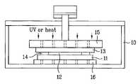
- a UV raymay be directed, and/or heat may be applied, to the seal in order to cure or harden and fix the first and second glass substrates 11 and 13 together ( 38 S).
- the substratesare large (e.g., 1.0 m ⁇ 1.2 m)
- misalignment of the two substratesmay occur during subsequent processes or during transfer after the bonding step. Therefore, the fixing is made for prevention of the misalignment of the bonded two substrates and maintaining a bonded state during the next process or transfer after the bonding.
- Fixing the two substratesoccurs within the bonding chamber under a vacuum or atmospheric pressure. Though it is preferable that the fixing is carried out after the bonding, the fixing may be carried out before the bonding is finished. For simplification of the process, though it is preferable that material of the fixing seal is the same as that of the main seal, material of fixing seal may be different from the main seal to improve efficiency in the fixing process.
- the fixing sealmay, for example, be a photosetting resin, a thermosetting resin, a UV-thermosetting resin, a pressure setting resin, or any other material with a high adhesive force.
- Fixing conditions used with the photosetting resinmay, for example, a UV ray having a power of 50–500 mW (e.g., 200 mW) directed for about 5–40 seconds (e.g., about 14 seconds).
- Fixing conditions used with the thermosetting resinmay be dependent on a material of the fixing seal and may, for example, include a setting temperature in a range of about 50–200° C. applied to the seal for more than about 10 seconds. Accordingly, the bonded substrate may be fixed by any one of light, heat, light and heat, and pressure.
- the fixing sealmay or may not be coated on the same substrate as the main seal.
- FIG. 4illustrates a seal layout pattern in accordance with a first embodiment of the present invention
- FIG. 10illustrates a section across a line I–I′ in FIG. 4 showing upper and lower stages and substrates.
- a method for fixing bonded substrates in accordance with a first embodiment of the present inventionincludes coating any of the aforementioned resins, forming a plurality of main seals 14 a on a periphery of each panel for bonding and sealing the liquid crystal between the two substrates, forming a dummy seal 14 b to surround a plurality of panels for protecting the main seals 14 a on an inner side thereof during bonding and pressing, and forming a plurality of fixing seals 14 c on an outer periphery of the dummy seal 14 b (an outer periphery of the substrate) at fixed intervals for fixing the two substrates preliminarily, which are removed during cutting, on the second glass substrate 13 in the foregoing seal 14 coating.
- the bonded two substratesmay then be fixed by forming the fixing seals 14 c , bonding the two substrates, directing a light (UV) to, and/or heating, the fixing seals 14 c thereby setting the fixing seals 14 c .
- the fixing seals 14 care formed from a the light (UV) setting resin, light (UV) may be directed to the fixing seals 14 c to fix the substrates.
- the fixing seals 14 care formed of a thermosetting resin, heat may be applied to the fixing seals 14 c for setting the fixing seals 14 c.
- the upper stage 15 and/or the lower stage 16includes a plurality of holes 17 for directing the light (UV) or applying heat.
- the fixing seals 14 c and the holes 17are aligned. Accordingly, upon directing a light (UV) or applying heat to the fixing seals 14 c from an upper stage side or a lower stage side through the holes 17 , the fixing seals 14 c are set, and the two substrates are fixed together.
- the light (UV) having a power of about 50–500 mW (e.g., 200 mW)is emitted from a light (UV) emitting pin ( 18 a or 18 b ) for about 5–40 seconds (e.g., about 14 seconds) that moves down from an upper side of the bonding chamber or moves up from a lower side of the bonding chamber.
- a heating device 18 a or 18 bmay be moved down from the upper side of the bonding chamber or moved up from the lower side of the bonding chamber to come into contact with a part of the first or second substrates 11 or 13 the fixing seals 14 c formed thereon through the holes 17 , and heats the fixing seals 14 c .
- the fixing seals 14 cmay be heated at a temperature of about 50–200° C. for about 10 seconds to selectively setting the fixing seals 14 c .
- light (UV) direction and the heat applicationmay be carried out simultaneously.
- the main seals 14 a , the dummy seal 14 b , and the fixing seals 14 cmay all be formed on the second glass substrate.
- the dummy seal 14 b and/or the fixing seals 14 cmay be formed on the first glass substrate 11 and/or the fixing seals 14 c may be formed of a material different from the main seals 14 a .
- either the main seals 14 amay be formed on the first substrate 11 while the dummy seal 14 b and/or the fixing seals 14 c may be formed on the second glass substrate, or the main seals 14 a may be formed on the second substrate 13 and the dummy seal 14 b and/or the fixing seals 14 c may be formed on the first glass substrate 11 .
- the main seals 14 a , the dummy seal 14 b , and the fixing seals 14 cmay all be formed on the first glass substrate 11 .
- FIG. 5illustrates a seal layout pattern in accordance with a second embodiment of the present invention.
- a method for fixing bonded substrates in accordance with a second embodiment of the present inventionincludes coating a resin selected from aforementioned materials (e.g., photosetting resin, a thermosetting resin, a UV-thermosetting resin, and a pressure setting resin), forming a plurality of main seals 14 a on a periphery of the second substrate for surrounding all the panels for bonding the two substrates and for sealing the liquid crystal between the two substrates, forming a dummy seal 14 b to surround a plurality of panels for protecting the main seals 14 a on an inner side thereof during bonding, and directing light (UV), and/or applying heat, to parts of the dummy seal 14 b for fixing the two substrates.
- a resin selected from aforementioned materialse.g., photosetting resin, a thermosetting resin, a UV-thermosetting resin, and a pressure setting resin
- the dummy seal 14 bmay be coated in the same region where the fixing seals are intended. Subsequently, light (UV) is directed, and/or heat is applied, to fix portions of the dummy seal 14 b corresponding to fixing seal locations.
- the conditions of light (UV) direction and/or heat applicationare the same as in the first embodiment.
- Reference numeral 14 ddenotes the regions in the dummy seal 14 b where the light (UV) is directed and/or the heat is applied. Accordingly, the dummy seal 14 b may be used to form fixing seals equivalent to those found in the first embodiment.
- FIG. 6illustrates a seal layout pattern in accordance with a third embodiment of the present invention.
- a method for fixing bonded substrates in accordance with a third preferred embodiment of the present inventionincludes omitting formation of the dummy seal. Accordingly, the two substrates may be fixed together by forming only the main seals 14 a and the fixing seals 14 c in a periphery of the substrate and directing a light (UV), applying heat, and/or pressure, to the fixing seals 14 c as similarly described in the first embodiment of the present invention. Further, the fixing seals 14 c may have a closed form, as with the dummy seal in the previous embodiments.
- FIG. 7illustrates a seal layout pattern in accordance with a fourth embodiment of the present invention.
- a method for fixing bonded substrates in accordance with a fourth embodiment of the present inventionfixes the two bonded substrates by forming the fixing seals 14 c in a periphery region of the substrate and also at fixed intervals in cutting regions between panels.
- LightUV
- may be directed and/or heat or pressuremay be applied to the fixing seals 14 c as with the third embodiment of the present invention.
- Other conditionsare the same with the first embodiment.
- FIG. 8illustrates a seal layout pattern in accordance with a fifth embodiment of the present invention.
- a method for fixing bonded substrates in accordance with a fifth embodiment of the present inventionfixes the two bonded substrates by forming a plurality of dummy seals that surround each of panels (main seals), forming the fixing seals 14 c in a periphery of the substrate, and directing a light (UV) and/or applying heat or pressure to the fixing seals 14 c as previously described with reference to the first embodiment of the present invention.
- Other conditionsare the same with the first embodiment.
- FIG. 9illustrates a seal layout pattern in accordance with a sixth embodiment of the present invention.
- a method for fixing bonded substrates in accordance with a sixth embodiment of the present inventionfixes the two bonded substrates by selectively directing light (UV) and/or applying heat to portions of a plurality of dummy seals 14 b formed on each panel. Light and/or heat may be selectively directed/applied to the dummy seals 14 b in accordance with the fifth embodiment of the present invention. Other conditions are the same with the first embodiment.
- the main seals 14 a , the dummy seals 14 b , and the fixing seals 14 cmay or may not be formed on the same substrate, and the main seals or the dummy seals may be formed on the substrate having the liquid crystal applied thereto.
- a method for fixing bonded substrates in accordance with a seventh embodiment of the present inventionfixes the two bonded substrates, not by forming separate dummy seals or fixing seals, but by selectively directing light (UV) and/or applying heat to portions of the main seals, wherein the main seals may be formed of a light (UV) setting resin, a thermosetting resin, or a light (UV) and thermosetting resin.
- a method for fixing bonded substrates in accordance with an eighth embodiment of the present inventionfixes the two bonded substrates by applying an adhesive, having a setting property better than that of the seals, to parts the fixing seals 14 c in the first, third, fourth, or fifth embodiment, and bonding the first and second glass substrates using the adhesive.
- misalignment of the bonded first and second glass substratesmay be prevented during transfer of the substrates for subsequent fabrication processes.
- the ESCwhen fixing of the two bonded substrates is finished, the ESC is turned off and the upper stage 15 is moved up. Accordingly, the upper stage 15 is separated from the fixed two glass substrates 11 and 13 .
- the substratesare unloaded in an unloading step ( 38 S) using the loader.
- the ESCmay be left on only in the upper stage and the fixed first and second glass substrates 11 and 13 are lifted by the upper stage.
- the loaderunloads the first and second glass substrates 11 and 13 from the upper stage 16 .
- one of the first and second glass substrates to be bonded in a next bonding processmay be loaded onto an empty stage while the fixed first and second glass substrates are unloaded.
- the fixed first and second glass substrates on the lower stage 16may be unloaded.
- the loadermay load a first glass substrate 11 to be bonded in a next bonding process onto the lower stage, and the fixed first and second glass substrates may be unloaded.
- a liquid crystal spreading processmay optionally be added before the process of unloading the bonded substrates where the liquid crystal between the fixed substrates may be spread, for example, toward the seal.
- a liquid crystal spreading processmay be carried out to evenly spread the liquid crystal toward the seal when the liquid crystal does not adequately spread after the unloading.
- the liquid crystal spreading processmay be carried out for more than 10 min. under atmospheric pressure or in a vacuum.
- the method for fabricating an LCD according to the present inventionhas the following advantages.
- applying the liquid crystal on the first substrate and coating the seal on the second substratepermits a balanced progression of the fabrication processes to the first and second substrates, thereby making efficient use of a production line.
- positioning the substrate receiver under the substrate and evacuation of the vacuum bonding chamberpermits the substrate affixed to the upper stage from falling down and breaking.
- the two staged evacuation of the vacuum bonding chamberprevents deformation of the substrate and air flow in the chamber caused by a sudden vacuum.
Landscapes
- Physics & Mathematics (AREA)
- Nonlinear Science (AREA)
- Mathematical Physics (AREA)
- Chemical & Material Sciences (AREA)
- Crystallography & Structural Chemistry (AREA)
- General Physics & Mathematics (AREA)
- Optics & Photonics (AREA)
- Liquid Crystal (AREA)
- Application Of Or Painting With Fluid Materials (AREA)
Abstract
Description
Claims (35)
Applications Claiming Priority (6)
| Application Number | Priority Date | Filing Date | Title |
|---|---|---|---|
| KRP2002-9096 | 2002-02-20 | ||
| KR2002-9096 | 2002-02-20 | ||
| KR10-2002-0009096AKR100510725B1 (en) | 2002-02-20 | 2002-02-20 | Method for manufacturing liquid crystal display device |
| KR1020020010170AKR100710153B1 (en) | 2002-02-26 | 2002-02-26 | Method for manufacturing liquid crystal display device |
| KRP2002-10170 | 2002-02-26 | ||
| KR2002-10170 | 2002-02-26 |
Publications (2)
| Publication Number | Publication Date |
|---|---|
| US20030156245A1 US20030156245A1 (en) | 2003-08-21 |
| US7365822B2true US7365822B2 (en) | 2008-04-29 |
Family
ID=27736661
Family Applications (1)
| Application Number | Title | Priority Date | Filing Date |
|---|---|---|---|
| US10/184,115Expired - LifetimeUS7365822B2 (en) | 2002-02-20 | 2002-06-28 | Method for fabricating LCD |
Country Status (3)
| Country | Link |
|---|---|
| US (1) | US7365822B2 (en) |
| JP (1) | JP4126593B2 (en) |
| CN (1) | CN100385300C (en) |
Cited By (3)
| Publication number | Priority date | Publication date | Assignee | Title |
|---|---|---|---|---|
| DE102009006822A1 (en)* | 2009-01-29 | 2010-09-16 | Fraunhofer-Gesellschaft zur Förderung der angewandten Forschung e.V. | Microstructure, process for its preparation, device for bonding a microstructure and microsystem |
| US9274381B2 (en) | 2011-12-23 | 2016-03-01 | Au Optronics Corporation | Fabrication method of a liquid crystal panel |
| US10788714B2 (en) | 2015-06-03 | 2020-09-29 | Samsung Display Co., Ltd. | Liquid crystal display and manufacturing method of the same |
Families Citing this family (14)
| Publication number | Priority date | Publication date | Assignee | Title |
|---|---|---|---|---|
| TWI275868B (en)* | 2003-11-24 | 2007-03-11 | Advanced Display Proc Eng Co | Substrate combining device and method |
| CN100334495C (en)* | 2004-06-30 | 2007-08-29 | 友达光电股份有限公司 | Frame glue repair method |
| KR101074389B1 (en)* | 2004-11-05 | 2011-10-17 | 엘지디스플레이 주식회사 | method for etching thin film and method for manufacturing of liquid crystal display device using the same |
| JP2006195128A (en)* | 2005-01-13 | 2006-07-27 | Ushio Inc | Panel bonding equipment |
| KR100977704B1 (en)* | 2007-12-21 | 2010-08-24 | 주성엔지니어링(주) | Display element and manufacturing method |
| JP5112151B2 (en)* | 2008-04-08 | 2013-01-09 | 株式会社アルバック | Light irradiation device |
| JP4623685B2 (en)* | 2009-03-26 | 2011-02-02 | 次世代モバイル用表示材料技術研究組合 | Manufacturing method of display device |
| CN102617025B (en)* | 2011-01-31 | 2014-06-25 | 洛阳兰迪玻璃机器股份有限公司 | Method for acquiring vacuum during making vacuum glass member |
| JP6056349B2 (en)* | 2012-10-09 | 2017-01-11 | 旭硝子株式会社 | Seal structure and method for manufacturing liquid crystal display panel member |
| JP5373168B2 (en)* | 2012-10-09 | 2013-12-18 | 株式会社アルバック | Light irradiation device |
| JP6144036B2 (en)* | 2012-11-22 | 2017-06-07 | イー インク コーポレイション | Display medium, display device |
| JP2017067874A (en)* | 2015-09-28 | 2017-04-06 | 株式会社ジャパンディスプレイ | Display device and manufacturing method thereof |
| CN107546250B (en)* | 2017-08-16 | 2020-02-14 | 武汉华星光电半导体显示技术有限公司 | Method and device for manufacturing OLED display panel |
| CN108646469A (en)* | 2018-05-03 | 2018-10-12 | 张家港康得新光电材料有限公司 | Panel and preparation method thereof, 2D/3D switchable apparatus can be switched in a kind of 2D/3D |
Citations (233)
| Publication number | Priority date | Publication date | Assignee | Title |
|---|---|---|---|---|
| JPS5165656A (en) | 1974-12-04 | 1976-06-07 | Shinshu Seiki Kk | |
| US3978580A (en) | 1973-06-28 | 1976-09-07 | Hughes Aircraft Company | Method of fabricating a liquid crystal display |
| US4094058A (en) | 1976-07-23 | 1978-06-13 | Omron Tateisi Electronics Co. | Method of manufacture of liquid crystal displays |
| JPS5738414A (en) | 1980-08-20 | 1982-03-03 | Showa Denko Kk | Spacer for display panel |
| JPS5788428A (en) | 1980-11-20 | 1982-06-02 | Ricoh Elemex Corp | Manufacture of liquid crystal display body device |
| JPS5827126A (en) | 1981-08-11 | 1983-02-17 | Nec Corp | Production of liquid crystal display panel |
| JPS5957221A (en) | 1982-09-28 | 1984-04-02 | Asahi Glass Co Ltd | Production of display element |
| JPS59195222A (en) | 1983-04-19 | 1984-11-06 | Matsushita Electric Ind Co Ltd | Manufacture of liquid-crystal panel |
| JPS60111221A (en) | 1983-11-19 | 1985-06-17 | Nippon Denso Co Ltd | Method and device for charging liquid crystal |
| JPS60164723A (en) | 1984-02-07 | 1985-08-27 | Seiko Instr & Electronics Ltd | Liquid crystal display device |
| JPS60217343A (en) | 1984-04-13 | 1985-10-30 | Matsushita Electric Ind Co Ltd | Liquid crystal display device and its preparation |
| JPS617822A (en) | 1984-06-22 | 1986-01-14 | Canon Inc | Production of liquid crystal element |
| JPS6155625A (en) | 1984-08-24 | 1986-03-20 | Nippon Denso Co Ltd | Manufacture of liquid crystal element |
| JPS6254229A (en) | 1985-07-15 | 1987-03-09 | Semiconductor Energy Lab Co Ltd | Manufacturing method for liquid crystal display |
| JPS6254228A (en) | 1985-07-15 | 1987-03-09 | Semiconductor Energy Lab Co Ltd | Manufacturing method for liquid crystal display |
| US4653864A (en) | 1986-02-26 | 1987-03-31 | Ovonic Imaging Systems, Inc. | Liquid crystal matrix display having improved spacers and method of making same |
| JPS6289025A (en) | 1985-10-15 | 1987-04-23 | Matsushita Electric Ind Co Ltd | Manufacturing method of liquid crystal display panel |
| JPS6290622A (en) | 1985-10-17 | 1987-04-25 | Seiko Epson Corp | liquid crystal display device |
| US4691995A (en) | 1985-07-15 | 1987-09-08 | Semiconductor Energy Laboratory Co., Ltd. | Liquid crystal filling device |
| JPS62205319A (en) | 1986-03-06 | 1987-09-09 | Canon Inc | Ferroelectric liquid crystal element |
| JPS63109413A (en) | 1986-10-27 | 1988-05-14 | Fujitsu Ltd | Manufacturing method of LCD display |
| JPS63110425A (en) | 1986-10-29 | 1988-05-14 | Toppan Printing Co Ltd | Cell for liquid crystal filling |
| JPS63128315A (en) | 1986-11-19 | 1988-05-31 | Victor Co Of Japan Ltd | Liquid crystal display element |
| US4775225A (en) | 1985-05-16 | 1988-10-04 | Canon Kabushiki Kaisha | Liquid crystal device having pillar spacers with small base periphery width in direction perpendicular to orientation treatment |
| JPS63311233A (en) | 1987-06-12 | 1988-12-20 | Toyota Motor Corp | lcd cell |
| JPH0273229A (en) | 1988-09-08 | 1990-03-13 | Seiko Epson Corp | Structure of liquid crystal display panel |
| JPH0536426A (en) | 1991-07-31 | 1993-02-12 | Mitsubishi Heavy Ind Ltd | Solid electrolytic fuel cell |
| JPH05107533A (en) | 1991-10-16 | 1993-04-30 | Shinetsu Eng Kk | Method for laminating glass substrate for liquid crystal display panel and laminating apparatus therefor |
| JPH05127179A (en) | 1991-11-01 | 1993-05-25 | Ricoh Co Ltd | Production of liquid crystal display element |
| JPH05154923A (en) | 1991-12-06 | 1993-06-22 | Hitachi Ltd | Substrate assembling device |
| US5247377A (en) | 1988-07-23 | 1993-09-21 | Rohm Gmbh Chemische Fabrik | Process for producing anisotropic liquid crystal layers on a substrate |
| JPH05265011A (en) | 1992-03-19 | 1993-10-15 | Seiko Instr Inc | Production of liquid crystal display element |
| JPH05281557A (en) | 1992-04-01 | 1993-10-29 | Matsushita Electric Ind Co Ltd | Liquid crystal panel manufacturing method |
| JPH05281562A (en) | 1992-04-01 | 1993-10-29 | Matsushita Electric Ind Co Ltd | Manufacture of liquid crystal panel |
| US5263888A (en) | 1992-02-20 | 1993-11-23 | Matsushita Electric Industrial Co., Ltd. | Method of manufacture of liquid crystal display panel |
| JPH0618829A (en) | 1992-06-30 | 1994-01-28 | Shinetsu Eng Kk | Device for laminating glass substrates for liquid crystal display boards |
| JPH0651256A (en) | 1992-07-30 | 1994-02-25 | Matsushita Electric Ind Co Ltd | Device for discharging liquid crystal |
| JPH0664229A (en) | 1992-08-24 | 1994-03-08 | Toshiba Corp | Optical printing head |
| JPH06148657A (en) | 1992-11-06 | 1994-05-27 | Matsushita Electric Ind Co Ltd | Method of manufacturing cell for liquid crystal display and manufacturing apparatus thereof |
| JPH06160871A (en) | 1992-11-26 | 1994-06-07 | Matsushita Electric Ind Co Ltd | Liquid crystal display panel and manufacturing method thereof |
| JPH06194637A (en) | 1992-12-24 | 1994-07-15 | Shinetsu Eng Kk | Method for sticking glass substrate for liquid crystal display plate |
| JPH06235925A (en) | 1993-02-10 | 1994-08-23 | Matsushita Electric Ind Co Ltd | Manufacture of liquid crystal display element |
| JPH06265915A (en) | 1993-03-12 | 1994-09-22 | Matsushita Electric Ind Co Ltd | Discharge device for filling liquid crystal |
| JPH06313870A (en) | 1993-04-28 | 1994-11-08 | Hitachi Ltd | Substrate assembly device |
| US5379139A (en) | 1986-08-20 | 1995-01-03 | Semiconductor Energy Laboratory Co., Ltd. | Liquid crystal device and method for manufacturing same with spacers formed by photolithography |
| JPH0784268A (en) | 1993-09-13 | 1995-03-31 | Hitachi Ltd | Sealing agent drawing method |
| US5406989A (en) | 1993-10-12 | 1995-04-18 | Ayumi Industry Co., Ltd. | Method and dispenser for filling liquid crystal into LCD cell |
| US5410423A (en)* | 1992-02-21 | 1995-04-25 | Canon Kabushiki Kaisha | Method of fabricating a liquid crystal panel using a dummy seal which is closed after hardening |
| JPH07128674A (en) | 1993-11-05 | 1995-05-19 | Matsushita Electric Ind Co Ltd | Liquid crystal display element manufacturing method |
| JPH07181507A (en) | 1993-12-21 | 1995-07-21 | Canon Inc | Liquid crystal display device and information transmission device including the liquid crystal display device |
| JPH07275770A (en) | 1994-04-06 | 1995-10-24 | Hitachi Techno Eng Co Ltd | Paste applicator |
| JPH07275771A (en) | 1994-04-11 | 1995-10-24 | Hitachi Techno Eng Co Ltd | Paste applicator |
| US5499128A (en) | 1993-03-15 | 1996-03-12 | Kabushiki Kaisha Toshiba | Liquid crystal display device with acrylic polymer spacers and method of manufacturing the same |
| JPH0876133A (en) | 1994-09-02 | 1996-03-22 | Shinetsu Eng Kk | Surface plate structure in a bonding apparatus for glass substrates for liquid crystal display boards |
| JPH0895066A (en) | 1994-09-27 | 1996-04-12 | Matsushita Electric Ind Co Ltd | Method and apparatus for manufacturing liquid crystal element |
| JPH08101395A (en) | 1994-09-30 | 1996-04-16 | Matsushita Electric Ind Co Ltd | Liquid crystal display element manufacturing method |
| US5507323A (en) | 1993-10-12 | 1996-04-16 | Fujitsu Limited | Method and dispenser for filling liquid crystal into LCD cell |
| JPH08106101A (en) | 1994-10-06 | 1996-04-23 | Fujitsu Ltd | Liquid crystal display panel manufacturing method |
| JPH08110504A (en) | 1994-10-13 | 1996-04-30 | Shinetsu Eng Kk | Glass substrate heating device for liquid crystal display panel |
| US5517344A (en)* | 1994-05-20 | 1996-05-14 | Prime View Hk Limited | System for protection of drive circuits formed on a substrate of a liquid crystal display |
| JPH08136937A (en) | 1994-11-09 | 1996-05-31 | Shinetsu Eng Kk | Method and apparatus for pressurizing and heating glass substrate for liquid crystal display panel |
| JPH08171094A (en) | 1994-12-19 | 1996-07-02 | Nippon Soken Inc | Liquid crystal injecting method and liquid crystal injecting device to liquid crystal display device |
| JPH08173874A (en) | 1994-12-26 | 1996-07-09 | Hitachi Techno Eng Co Ltd | Paste applicator |
| US5539545A (en) | 1993-05-18 | 1996-07-23 | Semiconductor Energy Laboratory Co., Ltd. | Method of making LCD in which resin columns are cured and the liquid crystal is reoriented |
| JPH08190099A (en) | 1995-01-11 | 1996-07-23 | Fujitsu Ltd | Liquid crystal display device manufacturing method and liquid crystal display device manufacturing apparatus |
| US5548429A (en) | 1993-06-14 | 1996-08-20 | Canon Kabushiki Kaisha | Process for producing liquid crystal device whereby curing the sealant takes place after pre-baking the substrates |
| JPH08240807A (en) | 1995-03-06 | 1996-09-17 | Fujitsu Ltd | Liquid crystal display panel sealing method |
| JPH091026A (en) | 1995-06-23 | 1997-01-07 | Hitachi Techno Eng Co Ltd | Paste applicator |
| JPH095762A (en) | 1995-06-20 | 1997-01-10 | Matsushita Electric Ind Co Ltd | Liquid crystal panel manufacturing method |
| JPH0926578A (en) | 1995-07-10 | 1997-01-28 | Fujitsu Ltd | Liquid crystal display panel and method of manufacturing the same |
| JPH0961829A (en) | 1995-08-21 | 1997-03-07 | Matsushita Electric Ind Co Ltd | Liquid crystal display element manufacturing method |
| JPH0973096A (en) | 1995-09-05 | 1997-03-18 | Matsushita Electric Ind Co Ltd | Liquid crystal display element manufacturing method |
| JPH0973075A (en) | 1995-09-05 | 1997-03-18 | Matsushita Electric Ind Co Ltd | Liquid crystal display element manufacturing method and liquid crystal display element manufacturing apparatus |
| JPH0994500A (en) | 1995-09-29 | 1997-04-08 | Hitachi Techno Eng Co Ltd | Paste applicator |
| JPH09127528A (en) | 1995-10-27 | 1997-05-16 | Fujitsu Ltd | Liquid crystal panel manufacturing method |
| US5642214A (en) | 1991-07-19 | 1997-06-24 | Sharp Kabushiki Kaisha | Optical modulating element and electronic apparatus using it |
| JPH09230357A (en) | 1996-02-22 | 1997-09-05 | Canon Inc | Liquid crystal panel manufacturing method and liquid crystal cell used therefor |
| US5668617A (en)* | 1995-01-27 | 1997-09-16 | Samsung Display Devices Co., Ltd. | Thin film-liquid crystal display panel and manufacturing method thereof |
| JPH09281511A (en) | 1996-04-17 | 1997-10-31 | Fujitsu Ltd | Liquid crystal display panel manufacturing method |
| JPH09311340A (en) | 1996-05-21 | 1997-12-02 | Matsushita Electric Ind Co Ltd | Liquid crystal display manufacturing method |
| US5742370A (en) | 1996-09-12 | 1998-04-21 | Korea Institute Of Science And Technology | Fabrication method for liquid crystal alignment layer by magnetic field treatment |
| JPH10123538A (en) | 1996-10-22 | 1998-05-15 | Matsushita Electric Ind Co Ltd | Manufacturing method of liquid crystal display element |
| JPH10123537A (en) | 1996-10-15 | 1998-05-15 | Matsushita Electric Ind Co Ltd | Liquid crystal display device and method of manufacturing the same |
| US5757451A (en) | 1995-09-08 | 1998-05-26 | Kabushiki Kaisha Toshiba | Liquid crystal display device spacers formed from stacked color layers |
| JPH10142616A (en) | 1996-11-14 | 1998-05-29 | Ayumi Kogyo Kk | Liquid crystal injection method and liquid dispenser |
| JPH10177178A (en) | 1996-12-17 | 1998-06-30 | Matsushita Electric Ind Co Ltd | Manufacturing method of liquid crystal display element |
| JPH10174924A (en) | 1996-12-17 | 1998-06-30 | Hitachi Techno Eng Co Ltd | Paste coating machine |
| JPH10221700A (en) | 1997-02-10 | 1998-08-21 | Fujitsu Ltd | Manufacturing method of liquid crystal display device |
| JPH10282512A (en) | 1997-04-07 | 1998-10-23 | Ayumi Kogyo Kk | Liquid crystal injection method and dispenser used therefor |
| JPH10333159A (en) | 1997-06-03 | 1998-12-18 | Matsushita Electric Ind Co Ltd | Liquid crystal display |
| JPH10333157A (en) | 1997-06-03 | 1998-12-18 | Matsushita Electric Ind Co Ltd | Manufacturing method of liquid crystal display device |
| US5852484A (en) | 1994-09-26 | 1998-12-22 | Matsushita Electric Industrial Co., Ltd. | Liquid crystal display panel and method and device for manufacturing the same |
| US5861932A (en) | 1997-03-31 | 1999-01-19 | Denso Corporation | Liquid crystal cell and its manufacturing method |
| JPH1114953A (en) | 1997-06-20 | 1999-01-22 | Matsushita Electric Ind Co Ltd | Method of manufacturing multi-touch liquid crystal display panel and multi-touch liquid crystal display panel |
| JPH1138424A (en) | 1997-07-23 | 1999-02-12 | Fujitsu Ltd | Liquid crystal display panel and method of manufacturing the same |
| US5875922A (en) | 1997-10-10 | 1999-03-02 | Nordson Corporation | Apparatus for dispensing an adhesive |
| JPH1164811A (en) | 1997-08-21 | 1999-03-05 | Matsushita Electric Ind Co Ltd | Method and apparatus for manufacturing liquid crystal display element |
| JPH11109388A (en) | 1997-10-03 | 1999-04-23 | Hitachi Ltd | Manufacturing method of liquid crystal display device |
| US5898041A (en)* | 1995-03-01 | 1999-04-27 | Matsushita Electric Industrial Co., Ltd. | Production process of liquid crystal display panel, seal material for liquid crystal cell and liquid crystal display |
| JPH11133438A (en) | 1997-10-24 | 1999-05-21 | Matsushita Electric Ind Co Ltd | Liquid crystal display device and its manufacturing method |
| JPH11142864A (en) | 1997-11-07 | 1999-05-28 | Matsushita Electric Ind Co Ltd | Manufacturing method of liquid crystal display device |
| JPH11174477A (en) | 1997-12-08 | 1999-07-02 | Matsushita Electric Ind Co Ltd | Manufacturing method of liquid crystal display device |
| JPH11212045A (en) | 1998-01-26 | 1999-08-06 | Matsushita Electric Ind Co Ltd | Liquid crystal panel manufacturing method |
| US5943113A (en)* | 1997-10-09 | 1999-08-24 | Fuji Photo Film Co., Ltd. | Method of producing a liquid crystal display unit |
| US5952678A (en) | 1995-01-23 | 1999-09-14 | Mitsubishi Denki Kabushiki Kaisha | SRAM cell with no PN junction between driver and load transistors and method of manufacturing the same |
| JPH11248930A (en) | 1998-03-06 | 1999-09-17 | Matsushita Electric Ind Co Ltd | Color filter substrate, method of manufacturing the color filter substrate, and liquid crystal display device using the color filter substrate |
| US5956112A (en) | 1995-10-02 | 1999-09-21 | Sharp Kabushiki Kaisha | Liquid crystal display device and method for manufacturing the same |
| JPH11264991A (en) | 1998-01-13 | 1999-09-28 | Matsushita Electric Ind Co Ltd | Manufacturing method of liquid crystal display element |
| JPH11262712A (en) | 1998-03-17 | 1999-09-28 | Hitachi Techno Eng Co Ltd | Paste application method and paste application machine |
| JPH11326922A (en) | 1998-05-14 | 1999-11-26 | Matsushita Electric Ind Co Ltd | Liquid crystal display panel manufacturing method |
| JPH11344714A (en) | 1998-06-02 | 1999-12-14 | Denso Corp | Liquid crystal cell |
| US6001203A (en) | 1995-03-01 | 1999-12-14 | Matsushita Electric Industrial Co., Ltd. | Production process of liquid crystal display panel, seal material for liquid crystal cell and liquid crystal display |
| US6011609A (en) | 1996-10-05 | 2000-01-04 | Samsung Electronics Co., Ltd. | Method of manufacturing LCD by dropping liquid crystals on a substrate and then pressing the substrates |
| JP2000002879A (en) | 1998-06-12 | 2000-01-07 | Matsushita Electric Ind Co Ltd | Apparatus and method for assembling liquid crystal panel |
| US6016178A (en) | 1996-09-13 | 2000-01-18 | Sony Corporation | Reflective guest-host liquid-crystal display device |
| US6016181A (en) | 1996-11-07 | 2000-01-18 | Sharp Kabushiki Kaisha | Liquid crystal device having column spacers with portion on each of the spacers for reflecting or absorbing visible light and method for fabricating the same |
| JP2000029035A (en) | 1998-07-09 | 2000-01-28 | Minolta Co Ltd | Liquid crystal element and its manufacture |
| JP2000047226A (en) | 1998-07-31 | 2000-02-18 | Matsushita Electric Ind Co Ltd | Liquid crystal display panel manufacturing method |
| JP2000056311A (en) | 1998-08-03 | 2000-02-25 | Matsushita Electric Ind Co Ltd | Liquid crystal display |
| JP2000066165A (en) | 1998-08-20 | 2000-03-03 | Matsushita Electric Ind Co Ltd | Liquid crystal display panel manufacturing method |
| JP2000066218A (en) | 1998-08-21 | 2000-03-03 | Shinetsu Engineering Kk | LCD panel manufacturing equipment |
| US6055035A (en) | 1998-05-11 | 2000-04-25 | International Business Machines Corporation | Method and apparatus for filling liquid crystal display (LCD) panels |
| JP2000137235A (en) | 1998-11-02 | 2000-05-16 | Matsushita Electric Ind Co Ltd | Liquid crystal substrate bonding method |
| EP1003066A1 (en) | 1998-11-16 | 2000-05-24 | Matsushita Electric Industrial Co., Ltd. | Method of manufacturing liquid crystal display devices |
| JP2000193988A (en) | 1998-12-25 | 2000-07-14 | Fujitsu Ltd | Method and apparatus for manufacturing liquid crystal display panel |
| JP2000241825A (en) | 1999-02-23 | 2000-09-08 | Seiko Epson Corp | Liquid crystal device manufacturing method |
| JP2000241824A (en) | 1999-02-18 | 2000-09-08 | Matsushita Electric Ind Co Ltd | Manufacturing method of liquid crystal display device |
| JP2000258782A (en) | 1999-03-08 | 2000-09-22 | Optrex Corp | Production of liquid crystal display device |
| JP2000284295A (en) | 1999-03-30 | 2000-10-13 | Hitachi Techno Eng Co Ltd | Substrate assembling method and apparatus |
| JP2000292799A (en) | 1999-04-09 | 2000-10-20 | Matsushita Electric Ind Co Ltd | Liquid crystal display device and method of manufacturing the same |
| JP2000310759A (en) | 1999-04-28 | 2000-11-07 | Matsushita Electric Ind Co Ltd | Liquid crystal display device manufacturing apparatus and method |
| JP2000310784A (en) | 1999-02-22 | 2000-11-07 | Matsushita Electric Ind Co Ltd | Liquid crystal panel, color filter and method for producing them |
| JP2000338501A (en) | 1999-05-26 | 2000-12-08 | Matsushita Electric Ind Co Ltd | Liquid crystal display panel manufacturing method |
| US6163357A (en)* | 1996-09-26 | 2000-12-19 | Kabushiki Kaisha Toshiba | Liquid crystal display device having the driving circuit disposed in the seal area, with different spacer density in driving circuit area than display area |
| JP2001005401A (en) | 1999-06-21 | 2001-01-12 | Hitachi Techno Eng Co Ltd | Substrate assembling method and apparatus |
| JP2001005405A (en) | 1999-06-18 | 2001-01-12 | Hitachi Techno Eng Co Ltd | Substrate assembling method and apparatus |
| JP2001013506A (en) | 1999-04-30 | 2001-01-19 | Matsushita Electric Ind Co Ltd | Liquid crystal display device and method of manufacturing the same |
| US6177976B1 (en)* | 1996-05-01 | 2001-01-23 | Nec Corporation | Liquid crystal display |
| JP2001033793A (en) | 1999-07-21 | 2001-02-09 | Matsushita Electric Ind Co Ltd | Liquid crystal display panel and method of manufacturing the same |
| JP2001042341A (en) | 1999-08-03 | 2001-02-16 | Hitachi Techno Eng Co Ltd | How to assemble a liquid crystal substrate |
| JP2001051284A (en) | 1999-08-10 | 2001-02-23 | Matsushita Electric Ind Co Ltd | Liquid crystal display device manufacturing equipment |
| JP2001066615A (en) | 2000-08-02 | 2001-03-16 | Matsushita Electric Ind Co Ltd | Manufacturing method of liquid crystal display device |
| JP2001091727A (en) | 1999-09-27 | 2001-04-06 | Matsushita Electric Ind Co Ltd | Method for manufacturing color filter substrate, color filter substrate and liquid crystal display device |
| US6219126B1 (en) | 1998-11-20 | 2001-04-17 | International Business Machines Corporation | Panel assembly for liquid crystal displays having a barrier fillet and an adhesive fillet in the periphery |
| JP2001117109A (en) | 1999-10-21 | 2001-04-27 | Matsushita Electric Ind Co Ltd | Manufacturing method of liquid crystal display device |
| JP2001117105A (en) | 1999-10-18 | 2001-04-27 | Toshiba Corp | Manufacturing method of liquid crystal display device |
| US6226067B1 (en) | 1997-10-03 | 2001-05-01 | Minolta Co., Ltd. | Liquid crystal device having spacers and manufacturing method thereof |
| JP2001133799A (en) | 1999-11-05 | 2001-05-18 | Fujitsu Ltd | Manufacturing method of liquid crystal display device |
| JP2001133794A (en) | 1999-11-01 | 2001-05-18 | Kyoritsu Kagaku Sangyo Kk | Sealing agent for dropping process of lcd panel |
| JP2001133745A (en) | 1999-11-08 | 2001-05-18 | Hitachi Techno Eng Co Ltd | Substrate assembling method and apparatus |
| US6236445B1 (en) | 1996-02-22 | 2001-05-22 | Hughes Electronics Corporation | Method for making topographic projections |
| JP2001142074A (en) | 1999-11-10 | 2001-05-25 | Hitachi Ltd | Liquid crystal display |
| JP2001147437A (en) | 1999-11-19 | 2001-05-29 | Nec Corp | Liquid crystal display panel and method of producing the same |
| JP2001154211A (en) | 1999-11-30 | 2001-06-08 | Hitachi Ltd | Liquid crystal panel and method of manufacturing the same |
| JP2001166310A (en) | 1999-12-08 | 2001-06-22 | Matsushita Electric Ind Co Ltd | Liquid crystal display panel manufacturing method |
| JP2001166272A (en) | 1999-12-09 | 2001-06-22 | Hitachi Techno Eng Co Ltd | Substrate assembling method and apparatus |
| JP2001174829A (en) | 1999-12-14 | 2001-06-29 | Nec Corp | Liquid crystal display panel and its producing method |
| JP2001183683A (en) | 1999-10-05 | 2001-07-06 | Matsushita Electric Ind Co Ltd | Liquid crystal display panel and method of manufacturing and driving the same |
| JP2001201750A (en) | 2000-01-14 | 2001-07-27 | Fujitsu Ltd | Liquid crystal display device and method of manufacturing the same |
| JP2001209056A (en) | 2000-01-25 | 2001-08-03 | Shinetsu Engineering Kk | LCD panel manufacturing equipment |
| JP2001209060A (en) | 2000-12-11 | 2001-08-03 | Fujitsu Ltd | Liquid crystal display panel manufacturing method |
| JP2001209052A (en) | 2000-01-24 | 2001-08-03 | Matsushita Electric Ind Co Ltd | Liquid crystal display device and method of manufacturing the same |
| JP2001209057A (en) | 2000-01-26 | 2001-08-03 | Shinetsu Engineering Kk | LCD panel manufacturing equipment |
| JP2001215459A (en) | 2000-02-02 | 2001-08-10 | Matsushita Electric Ind Co Ltd | Liquid crystal display device manufacturing equipment |
| JP2001222017A (en) | 1999-05-24 | 2001-08-17 | Fujitsu Ltd | Liquid crystal display device and method of manufacturing the same |
| JP2001235758A (en) | 2000-02-23 | 2001-08-31 | Fujitsu Ltd | Liquid crystal display panel and method of manufacturing the same |
| JP2001242471A (en) | 2000-02-29 | 2001-09-07 | Ran Technical Service Kk | Method and device for sticking substrate of liquid crystal panel |
| JP2001255542A (en) | 2000-03-14 | 2001-09-21 | Sharp Corp | Substrate bonding method and substrate bonding apparatus, and method and apparatus for manufacturing liquid crystal display element |
| JP2001264782A (en) | 2000-03-16 | 2001-09-26 | Ayumi Kogyo Kk | Filling method of mucous material between flat panel substrates |
| JP2001272640A (en) | 2000-03-27 | 2001-10-05 | Fujitsu Ltd | Liquid crystal dropping device and liquid crystal dropping method |
| US6300454B1 (en)* | 1998-07-23 | 2001-10-09 | Wacker-Chemie Gmbh | Liquid-crystalline nematic organosiloxanes which can be crosslinked to form optically anisotropic polymer layers |
| JP2001281678A (en) | 2000-03-29 | 2001-10-10 | Fujitsu Ltd | Manufacturing method of liquid crystal display device |
| JP2001281675A (en) | 2000-03-29 | 2001-10-10 | Matsushita Electric Ind Co Ltd | Manufacturing method of liquid crystal display device |
| JP2001281676A (en) | 2000-03-29 | 2001-10-10 | Kyocera Corp | Manufacturing method of liquid crystal display device |
| JP2001282126A (en) | 2000-03-30 | 2001-10-12 | Hitachi Techno Eng Co Ltd | Board assembly equipment |
| US6304306B1 (en) | 1995-02-17 | 2001-10-16 | Sharp Kabushiki Kaisha | Liquid crystal display device and method for producing the same |
| JP2001305563A (en) | 2000-04-19 | 2001-10-31 | Hitachi Techno Eng Co Ltd | Substrate bonding device |
| JP2001330840A (en) | 2000-05-18 | 2001-11-30 | Toshiba Corp | Manufacturing method of liquid crystal display element |
| JP2001330837A (en) | 2000-05-19 | 2001-11-30 | Matsushita Electric Ind Co Ltd | Hermetic structure, method of manufacturing the same, liquid crystal display device using the same, and method of manufacturing the same |
| JP2001337335A (en) | 2000-05-26 | 2001-12-07 | Toshiba Corp | Manufacturing method of liquid crystal display element |
| JP2001356353A (en) | 2001-04-24 | 2001-12-26 | Hitachi Industries Co Ltd | Board assembly equipment |
| JP2001356354A (en) | 2000-06-13 | 2001-12-26 | Matsushita Electric Ind Co Ltd | Manufacturing method of liquid crystal display element |
| US6337730B1 (en) | 1998-06-02 | 2002-01-08 | Denso Corporation | Non-uniformly-rigid barrier wall spacers used to correct problems caused by thermal contraction of smectic liquid crystal material |
| JP2002014360A (en) | 2000-06-29 | 2002-01-18 | Matsushita Electric Ind Co Ltd | Method and apparatus for manufacturing liquid crystal panel |
| JP2002023176A (en) | 2000-07-05 | 2002-01-23 | Seiko Epson Corp | Liquid crystal injection device and liquid crystal injection method |
| JP2002049045A (en) | 2000-08-03 | 2002-02-15 | Nec Corp | Method for manufacturing liquid crystal display panel |
| JP2002079160A (en) | 2000-09-04 | 2002-03-19 | Hitachi Industries Co Ltd | Paste coating machine |
| JP2002080321A (en) | 2000-06-20 | 2002-03-19 | Kyowa Hakko Kogyo Co Ltd | Cosmetic |
| JP2002082340A (en) | 2000-09-08 | 2002-03-22 | Fuji Xerox Co Ltd | Method for manufacturing flat panel display |
| JP2002090760A (en) | 2000-09-12 | 2002-03-27 | Matsushita Electric Ind Co Ltd | Liquid crystal display panel manufacturing apparatus and method |
| JP2002090759A (en) | 2000-09-18 | 2002-03-27 | Sharp Corp | Apparatus and method for manufacturing liquid crystal display element |
| JP2002107740A (en) | 2000-09-28 | 2002-04-10 | Sharp Corp | Method and apparatus for manufacturing liquid crystal display panel |
| JP2002122873A (en) | 2000-10-13 | 2002-04-26 | Stanley Electric Co Ltd | Liquid crystal device manufacturing method |
| JP2002122870A (en) | 2000-10-13 | 2002-04-26 | Fujitsu Ltd | Liquid crystal display device, manufacturing method thereof, and liquid crystal dropping device |
| JP2002122872A (en) | 2000-10-12 | 2002-04-26 | Hitachi Ltd | Liquid crystal display device and manufacturing method thereof |
| JP2002131762A (en) | 2000-10-30 | 2002-05-09 | Shinetsu Engineering Kk | Apparatus and method for bonding liquid crystal panel substrates |
| JP2002139734A (en) | 2000-10-31 | 2002-05-17 | Fujitsu Ltd | Method for manufacturing liquid crystal display device and apparatus for manufacturing liquid crystal display device |
| JP2002156518A (en) | 2000-11-16 | 2002-05-31 | Matsushita Electric Ind Co Ltd | Method for manufacturing color filter substrate |
| JP2002169167A (en) | 2000-12-05 | 2002-06-14 | Matsushita Electric Ind Co Ltd | Liquid crystal display device, manufacturing method thereof, and image display application device |
| JP2002169166A (en) | 2000-12-05 | 2002-06-14 | Matsushita Electric Ind Co Ltd | Liquid crystal display device, manufacturing method thereof, and image display application device |
| JP2002182222A (en) | 2000-12-19 | 2002-06-26 | Matsushita Electric Ind Co Ltd | Liquid crystal panel manufacturing method |
| US6414733B1 (en) | 1999-02-08 | 2002-07-02 | Dai Nippon Printing Co., Ltd. | Color liquid crystal display with a shielding member being arranged between sealing member and display zone |
| JP2002202512A (en) | 2000-12-28 | 2002-07-19 | Toshiba Corp | Liquid crystal display device and manufacturing method thereof |
| JP2002202514A (en) | 2000-12-28 | 2002-07-19 | Matsushita Electric Ind Co Ltd | Liquid crystal panel, method for manufacturing the same, and apparatus for manufacturing the same |
| JP2002209058A (en) | 2001-01-09 | 2002-07-26 | Canon Inc | Image reading apparatus and control method thereof |
| JP2002214626A (en) | 2001-01-17 | 2002-07-31 | Toshiba Corp | Manufacturing method of liquid crystal display device and sealing material |
| JP2002229042A (en) | 2001-02-06 | 2002-08-14 | Hitachi Industries Co Ltd | Substrate bonding equipment |
| JP2002236292A (en) | 2001-02-09 | 2002-08-23 | Matsushita Electric Ind Co Ltd | Liquid crystal panel manufacturing method and substrate bonding apparatus |
| JP2002236276A (en) | 2001-02-08 | 2002-08-23 | Hitachi Industries Co Ltd | Substrate assembling method and assembling apparatus |
| JP2002258299A (en) | 2001-02-28 | 2002-09-11 | Matsushita Electric Ind Co Ltd | Method and apparatus for manufacturing liquid crystal display device and liquid crystal display device |
| JP2002277881A (en) | 2001-03-16 | 2002-09-25 | Matsushita Electric Ind Co Ltd | Liquid crystal panel and method of manufacturing the same |
| JP2002277865A (en) | 2001-03-21 | 2002-09-25 | Matsushita Electric Ind Co Ltd | Liquid crystal display device and manufacturing method thereof |
| JP2002277866A (en) | 2001-03-21 | 2002-09-25 | Matsushita Electric Ind Co Ltd | Liquid crystal panel manufacturing method |
| JP2002287156A (en) | 2001-03-26 | 2002-10-03 | Matsushita Electric Ind Co Ltd | Method and apparatus for manufacturing liquid crystal panel |
| JP2002296605A (en) | 2001-03-30 | 2002-10-09 | Matsushita Electric Ind Co Ltd | Method of laminating liquid crystal substrates |
| JP2002311440A (en) | 2001-04-17 | 2002-10-23 | Hitachi Industries Co Ltd | Substrate bonding method and apparatus |
| JP2002311438A (en) | 2001-04-13 | 2002-10-23 | Matsushita Electric Ind Co Ltd | Method and apparatus for manufacturing liquid crystal display element |
| JP2002311442A (en) | 2001-04-17 | 2002-10-23 | Hitachi Industries Co Ltd | Liquid crystal substrate assembling method, assembling apparatus and liquid crystal supply apparatus |
| JP2002323687A (en) | 2001-04-25 | 2002-11-08 | Hitachi Industries Co Ltd | Liquid crystal substrate assembling method and its assembling apparatus |
| JP2002323694A (en) | 2001-04-24 | 2002-11-08 | Hitachi Industries Co Ltd | Substrate bonding method and bonding device |
| JP2002333635A (en) | 2001-05-07 | 2002-11-22 | Matsushita Electric Ind Co Ltd | Liquid crystal display device, method of manufacturing the same, and device for manufacturing liquid crystal display device |
| JP2002333843A (en) | 2001-05-10 | 2002-11-22 | Matsushita Electric Ind Co Ltd | Substrate bonding method and apparatus |
| JP2002333628A (en) | 2001-05-07 | 2002-11-22 | Matsushita Electric Ind Co Ltd | Liquid crystal display device, color filter substrate and array substrate |
| JP2002341357A (en) | 2001-05-14 | 2002-11-27 | Matsushita Electric Ind Co Ltd | Manufacturing method and manufacturing apparatus for liquid crystal display device |
| JP2002341355A (en) | 2001-05-16 | 2002-11-27 | Matsushita Electric Ind Co Ltd | Method for manufacturing liquid crystal display device, array substrate, and liquid crystal display device |
| JP2002341358A (en) | 2001-05-18 | 2002-11-27 | Matsushita Electric Ind Co Ltd | Liquid crystal display panel manufacturing method |
| JP2002341329A (en) | 2001-05-21 | 2002-11-27 | Matsushita Electric Ind Co Ltd | Liquid crystal display |
| JP2002341359A (en) | 2001-05-18 | 2002-11-27 | Matsushita Electric Ind Co Ltd | Method and apparatus for manufacturing liquid crystal display element |
| JP2002341356A (en) | 2001-05-18 | 2002-11-27 | Matsushita Electric Ind Co Ltd | Method and apparatus for forming gap in liquid crystal display panel |
| JP2002341362A (en) | 2001-05-18 | 2002-11-27 | Matsushita Electric Ind Co Ltd | Liquid crystal display panel manufacturing method and liquid crystal panel manufacturing apparatus |
| US6610364B1 (en)* | 2002-02-27 | 2003-08-26 | Lg. Philips Lcd Co., Ltd. | Apparatus for dispensing liquid crystal and method for controlling liquid crystal dropping amount |
| US6628365B1 (en)* | 2002-03-23 | 2003-09-30 | Lg.Philips Lcd Co., Ltd. | LCD with UV shielding part at dummy sealant region |
| US6661488B1 (en)* | 1997-06-12 | 2003-12-09 | Fujitsu Limited | Vertically-alligned (VA) liquid crystal display device |
Family Cites Families (3)
| Publication number | Priority date | Publication date | Assignee | Title |
|---|---|---|---|---|
| US3975580A (en)* | 1975-05-08 | 1976-08-17 | A. B. Chance Company | Articulated crossarm assembly for electrical conductor support structure |
| US4653884A (en)* | 1986-03-31 | 1987-03-31 | Polaroid Corporation | Foldable camera accessory for photographing electro-luminescent images |
| JP4689797B2 (en)* | 2000-07-19 | 2011-05-25 | Nec液晶テクノロジー株式会社 | Liquid crystal display device manufacturing apparatus and manufacturing method thereof |
- 2002
- 2002-06-28USUS10/184,115patent/US7365822B2/ennot_activeExpired - Lifetime
- 2002-06-28CNCNB021405328Apatent/CN100385300C/ennot_activeExpired - Fee Related
- 2002-06-28JPJP2002190241Apatent/JP4126593B2/ennot_activeExpired - Fee Related
Patent Citations (241)
| Publication number | Priority date | Publication date | Assignee | Title |
|---|---|---|---|---|
| US3978580A (en) | 1973-06-28 | 1976-09-07 | Hughes Aircraft Company | Method of fabricating a liquid crystal display |
| JPS5165656A (en) | 1974-12-04 | 1976-06-07 | Shinshu Seiki Kk | |
| US4094058A (en) | 1976-07-23 | 1978-06-13 | Omron Tateisi Electronics Co. | Method of manufacture of liquid crystal displays |
| JPS5738414A (en) | 1980-08-20 | 1982-03-03 | Showa Denko Kk | Spacer for display panel |
| JPS5788428A (en) | 1980-11-20 | 1982-06-02 | Ricoh Elemex Corp | Manufacture of liquid crystal display body device |
| JPS5827126A (en) | 1981-08-11 | 1983-02-17 | Nec Corp | Production of liquid crystal display panel |
| JPS5957221A (en) | 1982-09-28 | 1984-04-02 | Asahi Glass Co Ltd | Production of display element |
| JPS59195222A (en) | 1983-04-19 | 1984-11-06 | Matsushita Electric Ind Co Ltd | Manufacture of liquid-crystal panel |
| JPS60111221A (en) | 1983-11-19 | 1985-06-17 | Nippon Denso Co Ltd | Method and device for charging liquid crystal |
| JPS60164723A (en) | 1984-02-07 | 1985-08-27 | Seiko Instr & Electronics Ltd | Liquid crystal display device |
| JPS60217343A (en) | 1984-04-13 | 1985-10-30 | Matsushita Electric Ind Co Ltd | Liquid crystal display device and its preparation |
| JPS617822A (en) | 1984-06-22 | 1986-01-14 | Canon Inc | Production of liquid crystal element |
| JPS6155625A (en) | 1984-08-24 | 1986-03-20 | Nippon Denso Co Ltd | Manufacture of liquid crystal element |
| US4775225A (en) | 1985-05-16 | 1988-10-04 | Canon Kabushiki Kaisha | Liquid crystal device having pillar spacers with small base periphery width in direction perpendicular to orientation treatment |
| US4691995A (en) | 1985-07-15 | 1987-09-08 | Semiconductor Energy Laboratory Co., Ltd. | Liquid crystal filling device |
| JPS6254228A (en) | 1985-07-15 | 1987-03-09 | Semiconductor Energy Lab Co Ltd | Manufacturing method for liquid crystal display |
| JPS6254229A (en) | 1985-07-15 | 1987-03-09 | Semiconductor Energy Lab Co Ltd | Manufacturing method for liquid crystal display |
| JPS6289025A (en) | 1985-10-15 | 1987-04-23 | Matsushita Electric Ind Co Ltd | Manufacturing method of liquid crystal display panel |
| JPS6290622A (en) | 1985-10-17 | 1987-04-25 | Seiko Epson Corp | liquid crystal display device |
| US4653864A (en) | 1986-02-26 | 1987-03-31 | Ovonic Imaging Systems, Inc. | Liquid crystal matrix display having improved spacers and method of making same |
| JPS62205319A (en) | 1986-03-06 | 1987-09-09 | Canon Inc | Ferroelectric liquid crystal element |
| US5379139A (en) | 1986-08-20 | 1995-01-03 | Semiconductor Energy Laboratory Co., Ltd. | Liquid crystal device and method for manufacturing same with spacers formed by photolithography |
| JPS63109413A (en) | 1986-10-27 | 1988-05-14 | Fujitsu Ltd | Manufacturing method of LCD display |
| JPS63110425A (en) | 1986-10-29 | 1988-05-14 | Toppan Printing Co Ltd | Cell for liquid crystal filling |
| JPS63128315A (en) | 1986-11-19 | 1988-05-31 | Victor Co Of Japan Ltd | Liquid crystal display element |
| JPS63311233A (en) | 1987-06-12 | 1988-12-20 | Toyota Motor Corp | lcd cell |
| US5247377A (en) | 1988-07-23 | 1993-09-21 | Rohm Gmbh Chemische Fabrik | Process for producing anisotropic liquid crystal layers on a substrate |
| JPH0273229A (en) | 1988-09-08 | 1990-03-13 | Seiko Epson Corp | Structure of liquid crystal display panel |
| US5642214A (en) | 1991-07-19 | 1997-06-24 | Sharp Kabushiki Kaisha | Optical modulating element and electronic apparatus using it |
| JPH0536426A (en) | 1991-07-31 | 1993-02-12 | Mitsubishi Heavy Ind Ltd | Solid electrolytic fuel cell |
| JPH05107533A (en) | 1991-10-16 | 1993-04-30 | Shinetsu Eng Kk | Method for laminating glass substrate for liquid crystal display panel and laminating apparatus therefor |
| JPH05127179A (en) | 1991-11-01 | 1993-05-25 | Ricoh Co Ltd | Production of liquid crystal display element |
| JPH05154923A (en) | 1991-12-06 | 1993-06-22 | Hitachi Ltd | Substrate assembling device |
| US5263888A (en) | 1992-02-20 | 1993-11-23 | Matsushita Electric Industrial Co., Ltd. | Method of manufacture of liquid crystal display panel |
| US5410423A (en)* | 1992-02-21 | 1995-04-25 | Canon Kabushiki Kaisha | Method of fabricating a liquid crystal panel using a dummy seal which is closed after hardening |
| JPH05265011A (en) | 1992-03-19 | 1993-10-15 | Seiko Instr Inc | Production of liquid crystal display element |
| JPH05281562A (en) | 1992-04-01 | 1993-10-29 | Matsushita Electric Ind Co Ltd | Manufacture of liquid crystal panel |
| JPH05281557A (en) | 1992-04-01 | 1993-10-29 | Matsushita Electric Ind Co Ltd | Liquid crystal panel manufacturing method |
| US5511591A (en) | 1992-04-13 | 1996-04-30 | Fujitsu Limited | Method and dispenser for filling liquid crystal into LCD cell |
| JPH0618829A (en) | 1992-06-30 | 1994-01-28 | Shinetsu Eng Kk | Device for laminating glass substrates for liquid crystal display boards |
| JPH0651256A (en) | 1992-07-30 | 1994-02-25 | Matsushita Electric Ind Co Ltd | Device for discharging liquid crystal |
| JPH0664229A (en) | 1992-08-24 | 1994-03-08 | Toshiba Corp | Optical printing head |
| JPH06148657A (en) | 1992-11-06 | 1994-05-27 | Matsushita Electric Ind Co Ltd | Method of manufacturing cell for liquid crystal display and manufacturing apparatus thereof |
| JPH06160871A (en) | 1992-11-26 | 1994-06-07 | Matsushita Electric Ind Co Ltd | Liquid crystal display panel and manufacturing method thereof |
| JPH06194637A (en) | 1992-12-24 | 1994-07-15 | Shinetsu Eng Kk | Method for sticking glass substrate for liquid crystal display plate |
| JPH06235925A (en) | 1993-02-10 | 1994-08-23 | Matsushita Electric Ind Co Ltd | Manufacture of liquid crystal display element |
| JPH06265915A (en) | 1993-03-12 | 1994-09-22 | Matsushita Electric Ind Co Ltd | Discharge device for filling liquid crystal |
| US5499128A (en) | 1993-03-15 | 1996-03-12 | Kabushiki Kaisha Toshiba | Liquid crystal display device with acrylic polymer spacers and method of manufacturing the same |
| JPH06313870A (en) | 1993-04-28 | 1994-11-08 | Hitachi Ltd | Substrate assembly device |
| US5539545A (en) | 1993-05-18 | 1996-07-23 | Semiconductor Energy Laboratory Co., Ltd. | Method of making LCD in which resin columns are cured and the liquid crystal is reoriented |
| US5680189A (en) | 1993-05-18 | 1997-10-21 | Semiconductor Energy Laboratory Co., Ltd. | LCD columnar spacers made of a hydrophilic resin and LCD orientation film having a certain surface tension or alignment capability |
| US5548429A (en) | 1993-06-14 | 1996-08-20 | Canon Kabushiki Kaisha | Process for producing liquid crystal device whereby curing the sealant takes place after pre-baking the substrates |
| JPH0784268A (en) | 1993-09-13 | 1995-03-31 | Hitachi Ltd | Sealing agent drawing method |
| US5507323A (en) | 1993-10-12 | 1996-04-16 | Fujitsu Limited | Method and dispenser for filling liquid crystal into LCD cell |
| US5406989A (en) | 1993-10-12 | 1995-04-18 | Ayumi Industry Co., Ltd. | Method and dispenser for filling liquid crystal into LCD cell |
| JPH07128674A (en) | 1993-11-05 | 1995-05-19 | Matsushita Electric Ind Co Ltd | Liquid crystal display element manufacturing method |
| JPH07181507A (en) | 1993-12-21 | 1995-07-21 | Canon Inc | Liquid crystal display device and information transmission device including the liquid crystal display device |
| JPH07275770A (en) | 1994-04-06 | 1995-10-24 | Hitachi Techno Eng Co Ltd | Paste applicator |
| JPH07275771A (en) | 1994-04-11 | 1995-10-24 | Hitachi Techno Eng Co Ltd | Paste applicator |
| US5517344A (en)* | 1994-05-20 | 1996-05-14 | Prime View Hk Limited | System for protection of drive circuits formed on a substrate of a liquid crystal display |
| JPH0876133A (en) | 1994-09-02 | 1996-03-22 | Shinetsu Eng Kk | Surface plate structure in a bonding apparatus for glass substrates for liquid crystal display boards |
| US5854664A (en) | 1994-09-26 | 1998-12-29 | Matsushita Electric Industrial Co., Ltd. | Liquid crystal display panel and method and device for manufacturing the same |
| US5852484A (en) | 1994-09-26 | 1998-12-22 | Matsushita Electric Industrial Co., Ltd. | Liquid crystal display panel and method and device for manufacturing the same |
| JPH0895066A (en) | 1994-09-27 | 1996-04-12 | Matsushita Electric Ind Co Ltd | Method and apparatus for manufacturing liquid crystal element |
| JPH08101395A (en) | 1994-09-30 | 1996-04-16 | Matsushita Electric Ind Co Ltd | Liquid crystal display element manufacturing method |
| JPH08106101A (en) | 1994-10-06 | 1996-04-23 | Fujitsu Ltd | Liquid crystal display panel manufacturing method |
| JPH08110504A (en) | 1994-10-13 | 1996-04-30 | Shinetsu Eng Kk | Glass substrate heating device for liquid crystal display panel |
| JPH08136937A (en) | 1994-11-09 | 1996-05-31 | Shinetsu Eng Kk | Method and apparatus for pressurizing and heating glass substrate for liquid crystal display panel |
| JPH08171094A (en) | 1994-12-19 | 1996-07-02 | Nippon Soken Inc | Liquid crystal injecting method and liquid crystal injecting device to liquid crystal display device |
| JPH08173874A (en) | 1994-12-26 | 1996-07-09 | Hitachi Techno Eng Co Ltd | Paste applicator |
| JPH08190099A (en) | 1995-01-11 | 1996-07-23 | Fujitsu Ltd | Liquid crystal display device manufacturing method and liquid crystal display device manufacturing apparatus |
| US5952678A (en) | 1995-01-23 | 1999-09-14 | Mitsubishi Denki Kabushiki Kaisha | SRAM cell with no PN junction between driver and load transistors and method of manufacturing the same |
| US5668617A (en)* | 1995-01-27 | 1997-09-16 | Samsung Display Devices Co., Ltd. | Thin film-liquid crystal display panel and manufacturing method thereof |
| US6304306B1 (en) | 1995-02-17 | 2001-10-16 | Sharp Kabushiki Kaisha | Liquid crystal display device and method for producing the same |
| US5898041A (en)* | 1995-03-01 | 1999-04-27 | Matsushita Electric Industrial Co., Ltd. | Production process of liquid crystal display panel, seal material for liquid crystal cell and liquid crystal display |
| US6001203A (en) | 1995-03-01 | 1999-12-14 | Matsushita Electric Industrial Co., Ltd. | Production process of liquid crystal display panel, seal material for liquid crystal cell and liquid crystal display |
| JPH08240807A (en) | 1995-03-06 | 1996-09-17 | Fujitsu Ltd | Liquid crystal display panel sealing method |
| JPH095762A (en) | 1995-06-20 | 1997-01-10 | Matsushita Electric Ind Co Ltd | Liquid crystal panel manufacturing method |
| JPH091026A (en) | 1995-06-23 | 1997-01-07 | Hitachi Techno Eng Co Ltd | Paste applicator |
| JPH0926578A (en) | 1995-07-10 | 1997-01-28 | Fujitsu Ltd | Liquid crystal display panel and method of manufacturing the same |
| JPH0961829A (en) | 1995-08-21 | 1997-03-07 | Matsushita Electric Ind Co Ltd | Liquid crystal display element manufacturing method |
| JPH0973075A (en) | 1995-09-05 | 1997-03-18 | Matsushita Electric Ind Co Ltd | Liquid crystal display element manufacturing method and liquid crystal display element manufacturing apparatus |
| JPH0973096A (en) | 1995-09-05 | 1997-03-18 | Matsushita Electric Ind Co Ltd | Liquid crystal display element manufacturing method |
| US5757451A (en) | 1995-09-08 | 1998-05-26 | Kabushiki Kaisha Toshiba | Liquid crystal display device spacers formed from stacked color layers |
| JPH0994500A (en) | 1995-09-29 | 1997-04-08 | Hitachi Techno Eng Co Ltd | Paste applicator |
| US5956112A (en) | 1995-10-02 | 1999-09-21 | Sharp Kabushiki Kaisha | Liquid crystal display device and method for manufacturing the same |
| JPH09127528A (en) | 1995-10-27 | 1997-05-16 | Fujitsu Ltd | Liquid crystal panel manufacturing method |
| US6236445B1 (en) | 1996-02-22 | 2001-05-22 | Hughes Electronics Corporation | Method for making topographic projections |
| JPH09230357A (en) | 1996-02-22 | 1997-09-05 | Canon Inc | Liquid crystal panel manufacturing method and liquid crystal cell used therefor |
| JPH09281511A (en) | 1996-04-17 | 1997-10-31 | Fujitsu Ltd | Liquid crystal display panel manufacturing method |
| US6177976B1 (en)* | 1996-05-01 | 2001-01-23 | Nec Corporation | Liquid crystal display |
| JPH09311340A (en) | 1996-05-21 | 1997-12-02 | Matsushita Electric Ind Co Ltd | Liquid crystal display manufacturing method |
| US5742370A (en) | 1996-09-12 | 1998-04-21 | Korea Institute Of Science And Technology | Fabrication method for liquid crystal alignment layer by magnetic field treatment |
| US6016178A (en) | 1996-09-13 | 2000-01-18 | Sony Corporation | Reflective guest-host liquid-crystal display device |
| US6163357A (en)* | 1996-09-26 | 2000-12-19 | Kabushiki Kaisha Toshiba | Liquid crystal display device having the driving circuit disposed in the seal area, with different spacer density in driving circuit area than display area |
| US6011609A (en) | 1996-10-05 | 2000-01-04 | Samsung Electronics Co., Ltd. | Method of manufacturing LCD by dropping liquid crystals on a substrate and then pressing the substrates |
| JPH10123537A (en) | 1996-10-15 | 1998-05-15 | Matsushita Electric Ind Co Ltd | Liquid crystal display device and method of manufacturing the same |
| JPH10123538A (en) | 1996-10-22 | 1998-05-15 | Matsushita Electric Ind Co Ltd | Manufacturing method of liquid crystal display element |
| US6016181A (en) | 1996-11-07 | 2000-01-18 | Sharp Kabushiki Kaisha | Liquid crystal device having column spacers with portion on each of the spacers for reflecting or absorbing visible light and method for fabricating the same |
| JPH10142616A (en) | 1996-11-14 | 1998-05-29 | Ayumi Kogyo Kk | Liquid crystal injection method and liquid dispenser |
| JPH10177178A (en) | 1996-12-17 | 1998-06-30 | Matsushita Electric Ind Co Ltd | Manufacturing method of liquid crystal display element |
| JPH10174924A (en) | 1996-12-17 | 1998-06-30 | Hitachi Techno Eng Co Ltd | Paste coating machine |
| JPH10221700A (en) | 1997-02-10 | 1998-08-21 | Fujitsu Ltd | Manufacturing method of liquid crystal display device |
| US5861932A (en) | 1997-03-31 | 1999-01-19 | Denso Corporation | Liquid crystal cell and its manufacturing method |
| JPH10282512A (en) | 1997-04-07 | 1998-10-23 | Ayumi Kogyo Kk | Liquid crystal injection method and dispenser used therefor |
| JPH10333159A (en) | 1997-06-03 | 1998-12-18 | Matsushita Electric Ind Co Ltd | Liquid crystal display |
| JPH10333157A (en) | 1997-06-03 | 1998-12-18 | Matsushita Electric Ind Co Ltd | Manufacturing method of liquid crystal display device |
| US6661488B1 (en)* | 1997-06-12 | 2003-12-09 | Fujitsu Limited | Vertically-alligned (VA) liquid crystal display device |
| JPH1114953A (en) | 1997-06-20 | 1999-01-22 | Matsushita Electric Ind Co Ltd | Method of manufacturing multi-touch liquid crystal display panel and multi-touch liquid crystal display panel |
| JPH1138424A (en) | 1997-07-23 | 1999-02-12 | Fujitsu Ltd | Liquid crystal display panel and method of manufacturing the same |
| JPH1164811A (en) | 1997-08-21 | 1999-03-05 | Matsushita Electric Ind Co Ltd | Method and apparatus for manufacturing liquid crystal display element |
| US6226067B1 (en) | 1997-10-03 | 2001-05-01 | Minolta Co., Ltd. | Liquid crystal device having spacers and manufacturing method thereof |
| JPH11109388A (en) | 1997-10-03 | 1999-04-23 | Hitachi Ltd | Manufacturing method of liquid crystal display device |
| US5943113A (en)* | 1997-10-09 | 1999-08-24 | Fuji Photo Film Co., Ltd. | Method of producing a liquid crystal display unit |
| US5875922A (en) | 1997-10-10 | 1999-03-02 | Nordson Corporation | Apparatus for dispensing an adhesive |
| JPH11133438A (en) | 1997-10-24 | 1999-05-21 | Matsushita Electric Ind Co Ltd | Liquid crystal display device and its manufacturing method |
| JPH11142864A (en) | 1997-11-07 | 1999-05-28 | Matsushita Electric Ind Co Ltd | Manufacturing method of liquid crystal display device |
| JPH11174477A (en) | 1997-12-08 | 1999-07-02 | Matsushita Electric Ind Co Ltd | Manufacturing method of liquid crystal display device |
| US6222603B1 (en)* | 1998-01-13 | 2001-04-24 | Matsushita Electric Industrial Co., Ltd. | Method of manufacturing liquid crystal display device with a double seal |
| JPH11264991A (en) | 1998-01-13 | 1999-09-28 | Matsushita Electric Ind Co Ltd | Manufacturing method of liquid crystal display element |
| JPH11212045A (en) | 1998-01-26 | 1999-08-06 | Matsushita Electric Ind Co Ltd | Liquid crystal panel manufacturing method |
| JPH11248930A (en) | 1998-03-06 | 1999-09-17 | Matsushita Electric Ind Co Ltd | Color filter substrate, method of manufacturing the color filter substrate, and liquid crystal display device using the color filter substrate |
| JPH11262712A (en) | 1998-03-17 | 1999-09-28 | Hitachi Techno Eng Co Ltd | Paste application method and paste application machine |
| US6055035A (en) | 1998-05-11 | 2000-04-25 | International Business Machines Corporation | Method and apparatus for filling liquid crystal display (LCD) panels |
| JPH11326922A (en) | 1998-05-14 | 1999-11-26 | Matsushita Electric Ind Co Ltd | Liquid crystal display panel manufacturing method |
| US6337730B1 (en) | 1998-06-02 | 2002-01-08 | Denso Corporation | Non-uniformly-rigid barrier wall spacers used to correct problems caused by thermal contraction of smectic liquid crystal material |
| JPH11344714A (en) | 1998-06-02 | 1999-12-14 | Denso Corp | Liquid crystal cell |
| JP2000002879A (en) | 1998-06-12 | 2000-01-07 | Matsushita Electric Ind Co Ltd | Apparatus and method for assembling liquid crystal panel |
| JP2000029035A (en) | 1998-07-09 | 2000-01-28 | Minolta Co Ltd | Liquid crystal element and its manufacture |
| US6300454B1 (en)* | 1998-07-23 | 2001-10-09 | Wacker-Chemie Gmbh | Liquid-crystalline nematic organosiloxanes which can be crosslinked to form optically anisotropic polymer layers |
| JP2000047226A (en) | 1998-07-31 | 2000-02-18 | Matsushita Electric Ind Co Ltd | Liquid crystal display panel manufacturing method |
| JP2000056311A (en) | 1998-08-03 | 2000-02-25 | Matsushita Electric Ind Co Ltd | Liquid crystal display |
| JP2000066165A (en) | 1998-08-20 | 2000-03-03 | Matsushita Electric Ind Co Ltd | Liquid crystal display panel manufacturing method |
| JP2000066218A (en) | 1998-08-21 | 2000-03-03 | Shinetsu Engineering Kk | LCD panel manufacturing equipment |
| JP2000137235A (en) | 1998-11-02 | 2000-05-16 | Matsushita Electric Ind Co Ltd | Liquid crystal substrate bonding method |
| US6304311B1 (en)* | 1998-11-16 | 2001-10-16 | Matsushita Electric Industrial Co., Ltd. | Method of manufacturing liquid crystal display device |
| EP1003066A1 (en) | 1998-11-16 | 2000-05-24 | Matsushita Electric Industrial Co., Ltd. | Method of manufacturing liquid crystal display devices |
| JP2000147528A (en) | 1998-11-16 | 2000-05-26 | Matsushita Electric Ind Co Ltd | Manufacturing method of liquid crystal display element |
| US6219126B1 (en) | 1998-11-20 | 2001-04-17 | International Business Machines Corporation | Panel assembly for liquid crystal displays having a barrier fillet and an adhesive fillet in the periphery |
| JP2000193988A (en) | 1998-12-25 | 2000-07-14 | Fujitsu Ltd | Method and apparatus for manufacturing liquid crystal display panel |
| US6414733B1 (en) | 1999-02-08 | 2002-07-02 | Dai Nippon Printing Co., Ltd. | Color liquid crystal display with a shielding member being arranged between sealing member and display zone |
| JP2000241824A (en) | 1999-02-18 | 2000-09-08 | Matsushita Electric Ind Co Ltd | Manufacturing method of liquid crystal display device |
| JP2000310784A (en) | 1999-02-22 | 2000-11-07 | Matsushita Electric Ind Co Ltd | Liquid crystal panel, color filter and method for producing them |
| JP2000241825A (en) | 1999-02-23 | 2000-09-08 | Seiko Epson Corp | Liquid crystal device manufacturing method |
| JP2000258782A (en) | 1999-03-08 | 2000-09-22 | Optrex Corp | Production of liquid crystal display device |
| JP2000284295A (en) | 1999-03-30 | 2000-10-13 | Hitachi Techno Eng Co Ltd | Substrate assembling method and apparatus |
| JP2000292799A (en) | 1999-04-09 | 2000-10-20 | Matsushita Electric Ind Co Ltd | Liquid crystal display device and method of manufacturing the same |
| JP2000310759A (en) | 1999-04-28 | 2000-11-07 | Matsushita Electric Ind Co Ltd | Liquid crystal display device manufacturing apparatus and method |
| JP2001013506A (en) | 1999-04-30 | 2001-01-19 | Matsushita Electric Ind Co Ltd | Liquid crystal display device and method of manufacturing the same |
| JP2001222017A (en) | 1999-05-24 | 2001-08-17 | Fujitsu Ltd | Liquid crystal display device and method of manufacturing the same |
| JP2000338501A (en) | 1999-05-26 | 2000-12-08 | Matsushita Electric Ind Co Ltd | Liquid crystal display panel manufacturing method |
| JP2001005405A (en) | 1999-06-18 | 2001-01-12 | Hitachi Techno Eng Co Ltd | Substrate assembling method and apparatus |
| JP2001005401A (en) | 1999-06-21 | 2001-01-12 | Hitachi Techno Eng Co Ltd | Substrate assembling method and apparatus |
| JP2001033793A (en) | 1999-07-21 | 2001-02-09 | Matsushita Electric Ind Co Ltd | Liquid crystal display panel and method of manufacturing the same |
| JP2001042341A (en) | 1999-08-03 | 2001-02-16 | Hitachi Techno Eng Co Ltd | How to assemble a liquid crystal substrate |
| JP2001051284A (en) | 1999-08-10 | 2001-02-23 | Matsushita Electric Ind Co Ltd | Liquid crystal display device manufacturing equipment |
| JP2001091727A (en) | 1999-09-27 | 2001-04-06 | Matsushita Electric Ind Co Ltd | Method for manufacturing color filter substrate, color filter substrate and liquid crystal display device |
| JP2001183683A (en) | 1999-10-05 | 2001-07-06 | Matsushita Electric Ind Co Ltd | Liquid crystal display panel and method of manufacturing and driving the same |
| JP2001117105A (en) | 1999-10-18 | 2001-04-27 | Toshiba Corp | Manufacturing method of liquid crystal display device |
| JP2001117109A (en) | 1999-10-21 | 2001-04-27 | Matsushita Electric Ind Co Ltd | Manufacturing method of liquid crystal display device |
| JP2001133794A (en) | 1999-11-01 | 2001-05-18 | Kyoritsu Kagaku Sangyo Kk | Sealing agent for dropping process of lcd panel |
| JP2001133799A (en) | 1999-11-05 | 2001-05-18 | Fujitsu Ltd | Manufacturing method of liquid crystal display device |
| JP2001133745A (en) | 1999-11-08 | 2001-05-18 | Hitachi Techno Eng Co Ltd | Substrate assembling method and apparatus |
| JP2001142074A (en) | 1999-11-10 | 2001-05-25 | Hitachi Ltd | Liquid crystal display |
| JP2001147437A (en) | 1999-11-19 | 2001-05-29 | Nec Corp | Liquid crystal display panel and method of producing the same |
| JP2001154211A (en) | 1999-11-30 | 2001-06-08 | Hitachi Ltd | Liquid crystal panel and method of manufacturing the same |
| JP2001166310A (en) | 1999-12-08 | 2001-06-22 | Matsushita Electric Ind Co Ltd | Liquid crystal display panel manufacturing method |
| JP2001166272A (en) | 1999-12-09 | 2001-06-22 | Hitachi Techno Eng Co Ltd | Substrate assembling method and apparatus |
| JP2001174829A (en) | 1999-12-14 | 2001-06-29 | Nec Corp | Liquid crystal display panel and its producing method |
| JP2001201750A (en) | 2000-01-14 | 2001-07-27 | Fujitsu Ltd | Liquid crystal display device and method of manufacturing the same |
| JP2001209052A (en) | 2000-01-24 | 2001-08-03 | Matsushita Electric Ind Co Ltd | Liquid crystal display device and method of manufacturing the same |
| JP2001209056A (en) | 2000-01-25 | 2001-08-03 | Shinetsu Engineering Kk | LCD panel manufacturing equipment |
| JP2001209057A (en) | 2000-01-26 | 2001-08-03 | Shinetsu Engineering Kk | LCD panel manufacturing equipment |
| US20010021000A1 (en) | 2000-02-02 | 2001-09-13 | Norihiko Egami | Apparatus and method for manufacturing liquid crystal display |
| US6552772B2 (en)* | 2000-02-02 | 2003-04-22 | Matsushita Electric Industrial Co., Ltd. | Apparatus and method for manufacturing liquid crystal display using void-free elastic sheet |
| JP2001215459A (en) | 2000-02-02 | 2001-08-10 | Matsushita Electric Ind Co Ltd | Liquid crystal display device manufacturing equipment |
| JP2001235758A (en) | 2000-02-23 | 2001-08-31 | Fujitsu Ltd | Liquid crystal display panel and method of manufacturing the same |
| JP2001242471A (en) | 2000-02-29 | 2001-09-07 | Ran Technical Service Kk | Method and device for sticking substrate of liquid crystal panel |
| JP2001255542A (en) | 2000-03-14 | 2001-09-21 | Sharp Corp | Substrate bonding method and substrate bonding apparatus, and method and apparatus for manufacturing liquid crystal display element |
| JP2001264782A (en) | 2000-03-16 | 2001-09-26 | Ayumi Kogyo Kk | Filling method of mucous material between flat panel substrates |
| JP2001272640A (en) | 2000-03-27 | 2001-10-05 | Fujitsu Ltd | Liquid crystal dropping device and liquid crystal dropping method |
| JP2001281678A (en) | 2000-03-29 | 2001-10-10 | Fujitsu Ltd | Manufacturing method of liquid crystal display device |
| JP2001281675A (en) | 2000-03-29 | 2001-10-10 | Matsushita Electric Ind Co Ltd | Manufacturing method of liquid crystal display device |
| JP2001281676A (en) | 2000-03-29 | 2001-10-10 | Kyocera Corp | Manufacturing method of liquid crystal display device |
| JP2001282126A (en) | 2000-03-30 | 2001-10-12 | Hitachi Techno Eng Co Ltd | Board assembly equipment |
| JP2001305563A (en) | 2000-04-19 | 2001-10-31 | Hitachi Techno Eng Co Ltd | Substrate bonding device |
| JP2001330840A (en) | 2000-05-18 | 2001-11-30 | Toshiba Corp | Manufacturing method of liquid crystal display element |
| JP2001330837A (en) | 2000-05-19 | 2001-11-30 | Matsushita Electric Ind Co Ltd | Hermetic structure, method of manufacturing the same, liquid crystal display device using the same, and method of manufacturing the same |
| JP2001337335A (en) | 2000-05-26 | 2001-12-07 | Toshiba Corp | Manufacturing method of liquid crystal display element |
| JP2001356354A (en) | 2000-06-13 | 2001-12-26 | Matsushita Electric Ind Co Ltd | Manufacturing method of liquid crystal display element |
| JP2002080321A (en) | 2000-06-20 | 2002-03-19 | Kyowa Hakko Kogyo Co Ltd | Cosmetic |
| JP2002014360A (en) | 2000-06-29 | 2002-01-18 | Matsushita Electric Ind Co Ltd | Method and apparatus for manufacturing liquid crystal panel |
| JP2002023176A (en) | 2000-07-05 | 2002-01-23 | Seiko Epson Corp | Liquid crystal injection device and liquid crystal injection method |
| JP2001066615A (en) | 2000-08-02 | 2001-03-16 | Matsushita Electric Ind Co Ltd | Manufacturing method of liquid crystal display device |
| JP2002049045A (en) | 2000-08-03 | 2002-02-15 | Nec Corp | Method for manufacturing liquid crystal display panel |
| JP2002079160A (en) | 2000-09-04 | 2002-03-19 | Hitachi Industries Co Ltd | Paste coating machine |
| JP2002082340A (en) | 2000-09-08 | 2002-03-22 | Fuji Xerox Co Ltd | Method for manufacturing flat panel display |
| JP2002090760A (en) | 2000-09-12 | 2002-03-27 | Matsushita Electric Ind Co Ltd | Liquid crystal display panel manufacturing apparatus and method |
| JP2002090759A (en) | 2000-09-18 | 2002-03-27 | Sharp Corp | Apparatus and method for manufacturing liquid crystal display element |
| JP2002107740A (en) | 2000-09-28 | 2002-04-10 | Sharp Corp | Method and apparatus for manufacturing liquid crystal display panel |
| JP2002122872A (en) | 2000-10-12 | 2002-04-26 | Hitachi Ltd | Liquid crystal display device and manufacturing method thereof |
| JP2002122870A (en) | 2000-10-13 | 2002-04-26 | Fujitsu Ltd | Liquid crystal display device, manufacturing method thereof, and liquid crystal dropping device |
| JP2002122873A (en) | 2000-10-13 | 2002-04-26 | Stanley Electric Co Ltd | Liquid crystal device manufacturing method |
| JP2002131762A (en) | 2000-10-30 | 2002-05-09 | Shinetsu Engineering Kk | Apparatus and method for bonding liquid crystal panel substrates |
| JP2002139734A (en) | 2000-10-31 | 2002-05-17 | Fujitsu Ltd | Method for manufacturing liquid crystal display device and apparatus for manufacturing liquid crystal display device |
| JP2002156518A (en) | 2000-11-16 | 2002-05-31 | Matsushita Electric Ind Co Ltd | Method for manufacturing color filter substrate |
| JP2002169167A (en) | 2000-12-05 | 2002-06-14 | Matsushita Electric Ind Co Ltd | Liquid crystal display device, manufacturing method thereof, and image display application device |
| JP2002169166A (en) | 2000-12-05 | 2002-06-14 | Matsushita Electric Ind Co Ltd | Liquid crystal display device, manufacturing method thereof, and image display application device |
| JP2001209060A (en) | 2000-12-11 | 2001-08-03 | Fujitsu Ltd | Liquid crystal display panel manufacturing method |
| JP2002182222A (en) | 2000-12-19 | 2002-06-26 | Matsushita Electric Ind Co Ltd | Liquid crystal panel manufacturing method |
| JP2002202512A (en) | 2000-12-28 | 2002-07-19 | Toshiba Corp | Liquid crystal display device and manufacturing method thereof |
| JP2002202514A (en) | 2000-12-28 | 2002-07-19 | Matsushita Electric Ind Co Ltd | Liquid crystal panel, method for manufacturing the same, and apparatus for manufacturing the same |
| JP2002209058A (en) | 2001-01-09 | 2002-07-26 | Canon Inc | Image reading apparatus and control method thereof |
| JP2002214626A (en) | 2001-01-17 | 2002-07-31 | Toshiba Corp | Manufacturing method of liquid crystal display device and sealing material |
| JP2002229042A (en) | 2001-02-06 | 2002-08-14 | Hitachi Industries Co Ltd | Substrate bonding equipment |
| JP2002236276A (en) | 2001-02-08 | 2002-08-23 | Hitachi Industries Co Ltd | Substrate assembling method and assembling apparatus |
| JP2002236292A (en) | 2001-02-09 | 2002-08-23 | Matsushita Electric Ind Co Ltd | Liquid crystal panel manufacturing method and substrate bonding apparatus |
| JP2002258299A (en) | 2001-02-28 | 2002-09-11 | Matsushita Electric Ind Co Ltd | Method and apparatus for manufacturing liquid crystal display device and liquid crystal display device |
| JP2002277881A (en) | 2001-03-16 | 2002-09-25 | Matsushita Electric Ind Co Ltd | Liquid crystal panel and method of manufacturing the same |
| JP2002277865A (en) | 2001-03-21 | 2002-09-25 | Matsushita Electric Ind Co Ltd | Liquid crystal display device and manufacturing method thereof |
| JP2002277866A (en) | 2001-03-21 | 2002-09-25 | Matsushita Electric Ind Co Ltd | Liquid crystal panel manufacturing method |
| JP2002287156A (en) | 2001-03-26 | 2002-10-03 | Matsushita Electric Ind Co Ltd | Method and apparatus for manufacturing liquid crystal panel |
| JP2002296605A (en) | 2001-03-30 | 2002-10-09 | Matsushita Electric Ind Co Ltd | Method of laminating liquid crystal substrates |
| JP2002311438A (en) | 2001-04-13 | 2002-10-23 | Matsushita Electric Ind Co Ltd | Method and apparatus for manufacturing liquid crystal display element |
| JP2002311440A (en) | 2001-04-17 | 2002-10-23 | Hitachi Industries Co Ltd | Substrate bonding method and apparatus |
| JP2002311442A (en) | 2001-04-17 | 2002-10-23 | Hitachi Industries Co Ltd | Liquid crystal substrate assembling method, assembling apparatus and liquid crystal supply apparatus |
| JP2002323694A (en) | 2001-04-24 | 2002-11-08 | Hitachi Industries Co Ltd | Substrate bonding method and bonding device |
| JP2001356353A (en) | 2001-04-24 | 2001-12-26 | Hitachi Industries Co Ltd | Board assembly equipment |
| JP2002323687A (en) | 2001-04-25 | 2002-11-08 | Hitachi Industries Co Ltd | Liquid crystal substrate assembling method and its assembling apparatus |
| JP2002333635A (en) | 2001-05-07 | 2002-11-22 | Matsushita Electric Ind Co Ltd | Liquid crystal display device, method of manufacturing the same, and device for manufacturing liquid crystal display device |
| JP2002333628A (en) | 2001-05-07 | 2002-11-22 | Matsushita Electric Ind Co Ltd | Liquid crystal display device, color filter substrate and array substrate |
| JP2002333843A (en) | 2001-05-10 | 2002-11-22 | Matsushita Electric Ind Co Ltd | Substrate bonding method and apparatus |
| JP2002341357A (en) | 2001-05-14 | 2002-11-27 | Matsushita Electric Ind Co Ltd | Manufacturing method and manufacturing apparatus for liquid crystal display device |
| JP2002341355A (en) | 2001-05-16 | 2002-11-27 | Matsushita Electric Ind Co Ltd | Method for manufacturing liquid crystal display device, array substrate, and liquid crystal display device |
| JP2002341358A (en) | 2001-05-18 | 2002-11-27 | Matsushita Electric Ind Co Ltd | Liquid crystal display panel manufacturing method |
| JP2002341359A (en) | 2001-05-18 | 2002-11-27 | Matsushita Electric Ind Co Ltd | Method and apparatus for manufacturing liquid crystal display element |
| JP2002341356A (en) | 2001-05-18 | 2002-11-27 | Matsushita Electric Ind Co Ltd | Method and apparatus for forming gap in liquid crystal display panel |
| JP2002341362A (en) | 2001-05-18 | 2002-11-27 | Matsushita Electric Ind Co Ltd | Liquid crystal display panel manufacturing method and liquid crystal panel manufacturing apparatus |
| JP2002341329A (en) | 2001-05-21 | 2002-11-27 | Matsushita Electric Ind Co Ltd | Liquid crystal display |
| US6610364B1 (en)* | 2002-02-27 | 2003-08-26 | Lg. Philips Lcd Co., Ltd. | Apparatus for dispensing liquid crystal and method for controlling liquid crystal dropping amount |
| US6628365B1 (en)* | 2002-03-23 | 2003-09-30 | Lg.Philips Lcd Co., Ltd. | LCD with UV shielding part at dummy sealant region |
Cited By (5)
| Publication number | Priority date | Publication date | Assignee | Title |
|---|---|---|---|---|
| DE102009006822A1 (en)* | 2009-01-29 | 2010-09-16 | Fraunhofer-Gesellschaft zur Förderung der angewandten Forschung e.V. | Microstructure, process for its preparation, device for bonding a microstructure and microsystem |
| DE102009006822B4 (en)* | 2009-01-29 | 2011-09-01 | Fraunhofer-Gesellschaft zur Förderung der angewandten Forschung e.V. | Microstructure, process for its preparation, device for bonding a microstructure and microsystem |
| US8299630B2 (en) | 2009-01-29 | 2012-10-30 | Fraunhofer-Gesellschaft Zur Foerderung Der Angewandten Forschung E.V. | Microstructure with reactive bonding |
| US9274381B2 (en) | 2011-12-23 | 2016-03-01 | Au Optronics Corporation | Fabrication method of a liquid crystal panel |
| US10788714B2 (en) | 2015-06-03 | 2020-09-29 | Samsung Display Co., Ltd. | Liquid crystal display and manufacturing method of the same |
Also Published As
| Publication number | Publication date |
|---|---|
| CN100385300C (en) | 2008-04-30 |
| JP4126593B2 (en) | 2008-07-30 |
| JP2003241205A (en) | 2003-08-27 |
| US20030156245A1 (en) | 2003-08-21 |
| CN1439915A (en) | 2003-09-03 |
Similar Documents
| Publication | Publication Date | Title |
|---|---|---|
| US7426010B2 (en) | Method for fabricating LCD | |
| US7365822B2 (en) | Method for fabricating LCD | |
| US7040525B2 (en) | Stage structure in bonding machine and method for controlling the same | |
| US20060096709A1 (en) | LCD bonding machine and method for fabricating LCD by using the same | |
| US6784970B2 (en) | Method of fabricating LCD | |
| US7022199B2 (en) | Method for fabricating LCD | |
| US7230671B2 (en) | Method for fabricating liquid crystal display | |
| US6833901B2 (en) | Method for fabricating LCD having upper substrate coated with sealant | |
| US7372511B2 (en) | Device for controlling spreading of liquid crystal and method for fabricating an LCD | |
| US7230670B2 (en) | Method for fabricating LCD | |
| KR100741900B1 (en) | Method for manufacturing liquid crystal display device | |
| KR100710153B1 (en) | Method for manufacturing liquid crystal display device | |
| KR100463608B1 (en) | Method for manufacturing liquid crystal display device | |
| KR100510725B1 (en) | Method for manufacturing liquid crystal display device | |
| KR100769186B1 (en) | Manufacturing Method Of Liquid Crystal Display | |
| KR100710154B1 (en) | Method for manufacturing liquid crystal display device | |
| KR100510724B1 (en) | Method for manufacturing liquid crystal display device | |
| US20060065344A1 (en) | Substrate bonding apparatus for liquid crystal display device | |
| JP4087163B2 (en) | Manufacturing method of liquid crystal display device | |
| KR100796494B1 (en) | Manufacturing Method Of Liquid Crystal Display | |
| KR20030072503A (en) | Method for manufacturing liquid crystal display device | |
| KR20030071037A (en) | Method for manufacturing liquid crystal display device |
Legal Events
| Date | Code | Title | Description |
|---|---|---|---|
| AS | Assignment | Owner name:LG.PHILLPS LCD CO. LTD., KOREA, REPUBLIC OF Free format text:ASSIGNMENT OF ASSIGNORS INTEREST;ASSIGNORS:LEE, SANG S.;PARK, SANG H.;PARK, MOO Y.;AND OTHERS;REEL/FRAME:013385/0629 Effective date:20020901 | |
| FEPP | Fee payment procedure | Free format text:PAYER NUMBER DE-ASSIGNED (ORIGINAL EVENT CODE: RMPN); ENTITY STATUS OF PATENT OWNER: LARGE ENTITY Free format text:PAYOR NUMBER ASSIGNED (ORIGINAL EVENT CODE: ASPN); ENTITY STATUS OF PATENT OWNER: LARGE ENTITY | |
| STCF | Information on status: patent grant | Free format text:PATENTED CASE | |
| AS | Assignment | Owner name:LG DISPLAY CO., LTD., KOREA, REPUBLIC OF Free format text:CHANGE OF NAME;ASSIGNOR:LG.PHILIPS LCD CO., LTD.;REEL/FRAME:021754/0230 Effective date:20080304 Owner name:LG DISPLAY CO., LTD.,KOREA, REPUBLIC OF Free format text:CHANGE OF NAME;ASSIGNOR:LG.PHILIPS LCD CO., LTD.;REEL/FRAME:021754/0230 Effective date:20080304 | |
| FEPP | Fee payment procedure | Free format text:PAYER NUMBER DE-ASSIGNED (ORIGINAL EVENT CODE: RMPN); ENTITY STATUS OF PATENT OWNER: LARGE ENTITY Free format text:PAYOR NUMBER ASSIGNED (ORIGINAL EVENT CODE: ASPN); ENTITY STATUS OF PATENT OWNER: LARGE ENTITY | |
| FPAY | Fee payment | Year of fee payment:4 | |
| FPAY | Fee payment | Year of fee payment:8 | |
| MAFP | Maintenance fee payment | Free format text:PAYMENT OF MAINTENANCE FEE, 12TH YEAR, LARGE ENTITY (ORIGINAL EVENT CODE: M1553); ENTITY STATUS OF PATENT OWNER: LARGE ENTITY Year of fee payment:12 |