US7365602B2 - Multilevel power amplifier architecture using multi-tap transformer - Google Patents
Multilevel power amplifier architecture using multi-tap transformerDownload PDFInfo
- Publication number
- US7365602B2 US7365602B2US11/553,190US55319006AUS7365602B2US 7365602 B2US7365602 B2US 7365602B2US 55319006 AUS55319006 AUS 55319006AUS 7365602 B2US7365602 B2US 7365602B2
- Authority
- US
- United States
- Prior art keywords
- tap
- transformer
- input
- power
- power amplifier
- Prior art date
- Legal status (The legal status is an assumption and is not a legal conclusion. Google has not performed a legal analysis and makes no representation as to the accuracy of the status listed.)
- Expired - Lifetime
Links
- 238000004804windingMethods0.000claimsdescription96
- 238000004891communicationMethods0.000claimsdescription59
- 238000000034methodMethods0.000claimsdescription12
- 230000008878couplingEffects0.000claimsdescription10
- 238000010168coupling processMethods0.000claimsdescription10
- 238000005859coupling reactionMethods0.000claimsdescription10
- 239000010410layerSubstances0.000description32
- 238000012545processingMethods0.000description29
- 238000010586diagramMethods0.000description14
- 238000006243chemical reactionMethods0.000description10
- 230000003321amplificationEffects0.000description8
- 230000006870functionEffects0.000description8
- 238000003199nucleic acid amplification methodMethods0.000description8
- 230000010355oscillationEffects0.000description8
- 230000001413cellular effectEffects0.000description7
- 238000001914filtrationMethods0.000description7
- 238000001465metallisationMethods0.000description6
- 230000005540biological transmissionEffects0.000description5
- 238000013461designMethods0.000description5
- 230000010354integrationEffects0.000description4
- 238000005516engineering processMethods0.000description3
- 230000008901benefitEffects0.000description2
- 230000007423decreaseEffects0.000description2
- 239000002184metalSubstances0.000description2
- 230000008569processEffects0.000description2
- 238000011084recoveryMethods0.000description2
- VYPSYNLAJGMNEJ-UHFFFAOYSA-NSilicium dioxideChemical compoundO=[Si]=OVYPSYNLAJGMNEJ-UHFFFAOYSA-N0.000description1
- 230000004075alterationEffects0.000description1
- 239000000969carrierSubstances0.000description1
- 230000004907fluxEffects0.000description1
- 238000004519manufacturing processMethods0.000description1
- 238000013507mappingMethods0.000description1
- 239000000463materialSubstances0.000description1
- 238000010295mobile communicationMethods0.000description1
- 238000012986modificationMethods0.000description1
- 230000004048modificationEffects0.000description1
- 230000003071parasitic effectEffects0.000description1
- 230000009467reductionEffects0.000description1
- 230000001105regulatory effectEffects0.000description1
- 230000008054signal transmissionEffects0.000description1
- 229910052814silicon oxideInorganic materials0.000description1
- 239000002356single layerSubstances0.000description1
- 230000003068static effectEffects0.000description1
- 239000000126substanceSubstances0.000description1
- 238000006467substitution reactionMethods0.000description1
Images


Classifications
- H—ELECTRICITY
- H03—ELECTRONIC CIRCUITRY
- H03F—AMPLIFIERS
- H03F3/00—Amplifiers with only discharge tubes or only semiconductor devices as amplifying elements
- H03F3/60—Amplifiers in which coupling networks have distributed constants, e.g. with waveguide resonators
- H03F3/602—Combinations of several amplifiers
- H—ELECTRICITY
- H03—ELECTRONIC CIRCUITRY
- H03F—AMPLIFIERS
- H03F3/00—Amplifiers with only discharge tubes or only semiconductor devices as amplifying elements
- H03F3/20—Power amplifiers, e.g. Class B amplifiers, Class C amplifiers
- H03F3/21—Power amplifiers, e.g. Class B amplifiers, Class C amplifiers with semiconductor devices only
- H03F3/211—Power amplifiers, e.g. Class B amplifiers, Class C amplifiers with semiconductor devices only using a combination of several amplifiers
- H—ELECTRICITY
- H03—ELECTRONIC CIRCUITRY
- H03F—AMPLIFIERS
- H03F3/00—Amplifiers with only discharge tubes or only semiconductor devices as amplifying elements
- H03F3/45—Differential amplifiers
- H03F3/45071—Differential amplifiers with semiconductor devices only
- H03F3/45076—Differential amplifiers with semiconductor devices only characterised by the way of implementation of the active amplifying circuit in the differential amplifier
- H03F3/45179—Differential amplifiers with semiconductor devices only characterised by the way of implementation of the active amplifying circuit in the differential amplifier using MOSFET transistors as the active amplifying circuit
- H03F3/45183—Long tailed pairs
- H03F3/45188—Non-folded cascode stages
- H—ELECTRICITY
- H03—ELECTRONIC CIRCUITRY
- H03F—AMPLIFIERS
- H03F2200/00—Indexing scheme relating to amplifiers
- H03F2200/108—A coil being added in the drain circuit of a FET amplifier stage, e.g. for noise reducing purposes
- H—ELECTRICITY
- H03—ELECTRONIC CIRCUITRY
- H03F—AMPLIFIERS
- H03F2200/00—Indexing scheme relating to amplifiers
- H03F2200/372—Noise reduction and elimination in amplifier
- H—ELECTRICITY
- H03—ELECTRONIC CIRCUITRY
- H03F—AMPLIFIERS
- H03F2200/00—Indexing scheme relating to amplifiers
- H03F2200/541—Transformer coupled at the output of an amplifier
- H—ELECTRICITY
- H03—ELECTRONIC CIRCUITRY
- H03F—AMPLIFIERS
- H03F2203/00—Indexing scheme relating to amplifiers with only discharge tubes or only semiconductor devices as amplifying elements covered by H03F3/00
- H03F2203/45—Indexing scheme relating to differential amplifiers
- H03F2203/45731—Indexing scheme relating to differential amplifiers the LC comprising a transformer
Definitions
- the present inventionis directed in general to wireless communication technology.
- the present inventionrelates to transformers used with the radio communication transmitters and receivers.
- Communication systemsare known to support wireless and wire-lined communications between wireless and/or wire-lined communication devices. Such communication systems range from national and/or international cellular telephone systems to the Internet to point-to-point in-home wireless networks. Each type of communication system is constructed, and hence operates, in accordance with one or more communication standards. For instance, wireless communication systems may operate in accordance with one or more standards including, but not limited to, IEEE 802.11, Bluetooth (BT), advanced mobile phone services (AMPS), digital AMPS, global system for mobile communications (GSM), code division multiple access (CDMA), local multi-point distribution systems (LMDS), multi-channel-multi-point distribution systems (MMDS) and/or variations thereof.
- IEEE 802.11Bluetooth
- AMPSadvanced mobile phone services
- GSMglobal system for mobile communications
- CDMAcode division multiple access
- LMDSlocal multi-point distribution systems
- MMDSmulti-channel-multi-point distribution systems
- Wireless communication devicestypically communicate with one another using a radio transceiver (i.e., receiver and transmitter) that includes a transmitter section, a receiver section, a transformer for the receiver section, a transformer for the transmitter section, an antenna switch, and an antenna, all or part of which may be incorporated in, or coupled to, the wireless communication device.
- the antennareceives RF signals that are then coupled to the receiver section by the antenna switch.
- the antennaalso transmits amplified RF signals received from the transmitter section via the antenna switch.
- the receiver and transmitter transformersmay be implemented as a balun (balanced/unbalanced) transformer which is generally used to convert single ended signals into differential signals and conversely to convert differential signals into single ended signals.
- RF signals received via the antennaare converted into differential signals, which are provided to a low noise amplifier of the receiver section.
- differential signals from a power amplifier of the transmitter sectionare converted into single ended signals, which are provided to the antenna.
- the transmitter sectiontypically includes a data modulation stage, one or more intermediate frequency stages and a power amplifier.
- the data modulation stageconverts raw data into baseband signals in accordance with a particular wireless communication standard.
- the intermediate frequency stagesmix the baseband signals with one or more local oscillations to produce RF signals.
- conversion directly between baseband signals and RF signalsis performed.
- the power amplifieramplifies the RF signals prior to transmission via an antenna.
- the receiver sectiontypically includes a low noise amplifier, one or more intermediate frequency stages, a filtering stage and a data recovery stage.
- the low noise amplifierreceives inbound RF signals via the antenna and amplifies them.
- the intermediate frequency stagesmix the amplified RF signals with one or more local oscillations to convert the amplified RF signal into baseband signals or intermediate frequency (IF) signals.
- the filtering stagefilters the baseband signals or the IF signals to attenuate unwanted out of band signals to produce filtered signals.
- the data recovery stagerecovers raw data from the filtered signals in accordance with the particular wireless communication standard.
- VLSIVery Large Scale Integration
- inductorsare included in the mixers in the IF stages of both the receiver and transmitter, the power amplifier, a voltage control oscillator of a local oscillation module, the low noise amplifier, and the filters each include one or more inductors.
- Many attemptshave been made to integrate transformers and/or transformer baluns onto radio frequency integrated circuits; however, such integration has been limited due to flux leakage, capacitive coupling limits, and significant series resistance.
- transformer IC designsincluding coplanar interleaved transformers, toroidal and concentric transformers, overlay transformers and symmetric coplanar transformers
- coplanar interleaved transformerssuffer from a low quality (Q) factor have small coupling coefficients.
- Qquality
- Another drawback of conventional power amplifier architecture solutionsis that they do not efficiently provide power at all power levels required by differing applications.
- conventional power amplifier solutionsare designed to have maximum efficiency at the highest desired output level, so that when the power level is reduced from its maximum level, the power efficiency is also reduced. As a result, conventional power amplifier solutions do not allow for power output efficiency to be maintained across multiple power levels.
- an improved impedance matching system for use in power amplifier applicationswhereby power amplifier efficiency is maintained as the power level changes.
- a power amplification method and systemthat is capable of performing the above functions and overcoming these difficulties using circuitry implemented in integrated circuit form.
- the present inventionprovides an improved power amplifier architecture and methodology using a multi-tap transformer and inductor to control power transmission at different levels while maintaining efficiency.
- a transformer having “N” tapsmay be used to provide “N” different impedance levels by connecting the transformer between a plurality of amplifier cells and an output load. By connecting each transformer tap to an amplifier cell, power from that cell is delivered through the transformer to the output load in such a way that power efficiency is maintained, regardless of which of the “N” amplifier cells is turned on at once.
- any one of the “N” amplifier cellscan be turned on at once along with any combination of the “N” amplifier cells to achieve intermediate power levels between the power steps provided by each of the “N” power amplifier cells.
- an on-chip multi-tap transformerfor efficiently delivering power from a plurality of power amplifiers to a shared output impedance (such as an antenna) through an on-chip multiple tap transformer, all on a single CMOS integrated circuit wireless communications device.
- the multi-tap transformermay include a primary winding formed on a first layer of an integrated circuit that is coupled to the shared output impedance.
- the multi-tap transformermay also include a secondary winding that is formed on a second layer of the integrated circuit, and that includes a plurality of input taps, where each input tap is coupled to one of a plurality of power amplifiers.
- the secondary windingmay have a generally octagonal geometric shape, and may include a common node (coupled to a ground reference potential), a first portion, a second portion, where each portion has one node, a first tap and a second tap.
- the nodes from the first and second portionsmay be coupled to receive a first differential input signal
- the first taps of the first and second portionsmay be coupled to receive a second differential input signal
- the second taps of the first and second portionsmay be coupled to receive a third differential input signal.
- each input tapprovides a different, predetermined impedance level for connecting the power amplifier coupled to the input tap through to the shared output impedance.
- a plurality of differential input signals or single-ended input signalsmay be applied to the multi-tap transformer, and any one or more of the input signals from the power amplifiers can be turned on at once using the variable load impedance of the multi-tap transformer.
- FIG. 1is a schematic block diagram of a wireless communication system in accordance with an illustrative embodiment of the present invention.
- FIG. 2is a schematic block diagram of a wireless communication device in accordance with an illustrative embodiment of the present invention.
- FIG. 3is a simplified schematic block diagram of a power amplifier that is provided for illustration purposes.
- FIG. 4is a simplified schematic block diagram of an exemplary power amplification system that connects a plurality of different power amplifiers through a multi-tap transformer to a shared output load in accordance with an illustrative embodiment of the present invention.
- FIG. 5is a simplified schematic block diagram of an exemplary power amplification system that connects a plurality of differential power amplifiers to a multi-tap transformer in accordance with an illustrative embodiment of the present invention.
- FIG. 6is a schematic diagram of a multi-tap transformer in accordance with an illustrative embodiment of the present invention.
- FIG. 7is a schematic diagram of an alternate multiple tap transformer balun in accordance with an illustrative embodiment of the present invention.
- FIG. 8illustrates a top view of a multi-tap secondary winding of a multi-tap transformer balun or inductor in accordance with an illustrative embodiment of the present invention.
- FIG. 9illustrates a cross sectional view of a multi-tap transformer balun or inductor in accordance with an illustrative embodiment of the present invention.
- FIG. 10illustrates a bottom view of a primary winding of an on-chip multi-tap transformer balun in accordance with an illustrative embodiment of the present invention.
- FIG. 11illustrates a cross sectional view of a multi-layered multiple tap transformer balun in accordance with an illustrative embodiment of the present invention.
- FIG. 12illustrates a cross sectional view of an alternate multi-layered multi-tap transformer balun in accordance with an illustrative embodiment of the present invention.
- FIG. 13depicts an alternate secondary winding for an on-chip multi-tap transformer balun or an on-chip multi-tap inductor in accordance with an illustrative embodiment of the present invention.
- FIG. 14is a cross sectional view of a single layer differential inductor in accordance with an illustrative embodiment of the present invention.
- FIG. 15is a cross sectional view of a shunted differential inductor in accordance with an illustrative embodiment of the present invention.
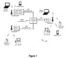
- FIG. 1illustrates a wireless communication system 10 in which embodiments of the present invention may operate.
- the wireless communication system 10includes a plurality of base stations and/or access points 12 , 14 , 16 , a plurality of wireless communication devices 18 - 32 and a network hardware component 34 .
- the wireless communication devices 18 - 32may be laptop host computers 18 and 26 , personal digital assistant hosts 20 and 30 , personal computer hosts 32 , cellular telephone hosts 28 , an 802.11a WLAN device 22 and/or an 802.11 g WLAN device 24 .
- the details of the wireless communication deviceswill be described in greater detail with reference to FIGS. 2-15 .
- the base stations or access points 12 , 14 , 16are operably coupled to the network hardware 34 via local area network connections 36 , 38 , 40 .
- the network hardware 34(which may be a router, switch, bridge, modem, system controller, etc.) provides a wide area network connection 42 for the communication system 10 .
- Each of the base stations or access points 12 , 14 , 16has an associated antenna or antenna array to communicate with the wireless communication devices in its area.
- the wireless communication devicesregister with a particular base station or access point 12 , 14 , 16 to receive services from the communication system 10 .
- For direct connectionsi.e., point-to-point communications
- wireless communication devicescommunicate directly via an allocated channel.
- each wireless communication deviceincludes a built-in radio and/or is coupled to a radio.
- the radioincludes a highly linear amplifier and/or programmable multi-stage amplifier as disclosed herein to enhance performance, reduce costs, reduce size, and/or enhance broadband applications.
- FIG. 2is a schematic block diagram illustrating a wireless communication device that includes the host device 51 and an associated radio 60 .
- the radio 60is a built-in component.
- the radio 60may be built-in or an externally coupled component.
- the host device 51includes a processing module 50 , memory 52 , radio interface 54 , input interface 58 and output interface 56 .
- the processing module 50 and memory 52execute the corresponding instructions that are typically done by the host device. For example, for a cellular telephone host device, the processing module 50 performs the corresponding communication functions in accordance with a particular cellular telephone standard.
- the radio interface 54allows data to be received from and sent to the radio 60 .
- the radio interface 54For data received from the radio 60 (e.g., inbound data), the radio interface 54 provides the data to the processing module 50 for further processing and/or routing to the output interface 56 .
- the output interface 56provides connectivity to an output display device (such as a display, monitor, speakers, etc.) such that the received data may be displayed.
- the radio interface 54also provides data from the processing module 50 to the radio 60 .
- the processing module 50may receive the outbound data from an input device (such as a keyboard, keypad, microphone, etc.) via the input interface 58 or generate the data itself.
- the processing module 50may perform a corresponding host function on the data and/or route it to the radio 60 via the radio interface 54 .
- Radio 60includes a host interface 62 , digital receiver processing module 64 , an analog-to-digital converter 66 , a filtering/attenuation module 68 , an IF mixing down-conversion stage 70 , a receiver filter 71 , a low noise amplifier 72 , a transmitter/receiver switch 73 , a local oscillation module 74 , memory 75 , a digital transmitter processing module 76 , a digital-to-analog converter 78 , a filtering/gain module 80 , an IF mixing up-conversion stage 82 , a power amplifier 84 , a transmitter filter module 85 , and an antenna 86 .
- the antenna 86may be a single antenna that is shared by the transmit and receive paths as regulated by the Tx/Rx switch 73 , or may include separate antennas for the transmit path and receive path.
- the antenna implementationwill depend on the particular standard to which the wireless communication device is compliant.
- the digital receiver processing module 64 and the digital transmitter processing module 76in combination with operational instructions stored in memory 75 , execute digital receiver functions and digital transmitter functions, respectively.
- the digital receiver functionsinclude, but are not limited to, digital intermediate frequency to baseband conversion, demodulation, constellation demapping, decoding, and/or descrambling.
- the digital transmitter functionsinclude, but are not limited to, scrambling, encoding, constellation mapping, modulation, and/or digital baseband to IF conversion.
- the digital receiver and transmitter processing modules 64 and 76may be implemented using a shared processing device, individual processing devices, or a plurality of processing devices.
- Such a processing devicemay be a microprocessor, micro-controller, digital signal processor, microcomputer, central processing unit, field programmable gate array, programmable logic device, state machine, logic circuitry, analog circuitry, digital circuitry, and/or any device that manipulates signals (analog and/or digital) based on operational instructions.
- the memory 75may be a single memory device or a plurality of memory devices.
- Such a memory devicemay be a read-only memory, random access memory, volatile memory, non-volatile memory, static memory, dynamic memory, flash memory, and/or any device that stores digital information.
- the memory storing the corresponding operational instructionsmay be embedded with the circuitry comprising the state machine, analog circuitry, digital circuitry, and/or logic circuitry.
- the radio 60receives outbound data 94 from the host device via the host interface 62 .
- the host interface 62routes the outbound data 94 to the digital transmitter processing module 76 , which processes the outbound data 94 in accordance with a particular wireless communication standard (e.g., IEEE 802.11a/b/g, Bluetooth, etc.) to produce digital transmission formatted data 96 .
- the digital transmission formatted data 96will be a digital baseband signal or a digital low IF signal, where the low IF typically will be in the frequency range of one hundred kilohertz to a few megahertz.
- the digital-to-analog converter 78converts the digital transmission formatted data 96 from the digital domain to the analog domain.
- the filtering/gain module 80which may be implemented in accordance with the teachings of the present invention, filters and/or adjusts the gain of the analog signal prior to providing it to the IF mixing stage 82 .
- the IF mixing stage 82which may be implemented in accordance with the teachings of the present invention, directly converts the analog baseband or low IF signal into an RF signal based on a transmitter local oscillation 83 provided by local oscillation module 74 .
- the power amplifier 84which may be implemented in accordance with the teachings of the present invention, amplifies the RF signal to produce an amplified outbound RF signal.
- the amplified outbound RF signalis filtered by the transmitter filter module 85 , which may be implemented in accordance with the teachings of the present invention.
- the antenna 86transmits the outbound RF signal 98 to a targeted device such as a base station, an access point and/or another wireless communication device.
- the radio 60also receives an inbound RF signal 88 via the antenna 86 , which was transmitted by a base station, an access point, or another wireless communication device.
- the antenna 86provides the inbound RF signal 88 to the receiver filter module 71 via the Tx/Rx switch 73 , where the Rx filter 71 , which may be implemented in accordance with the teachings of the present invention, bandpass filters the inbound RF signal 88 .
- the Rx filter 71provides the filtered RF signal to low noise amplifier 72 , which amplifies the signal 88 to produce an amplified inbound RF signal.
- the low noise amplifier 72which may be implemented in accordance with the teachings of the present invention, provides the amplified inbound RF signal to the IF mixing module 70 , which directly converts the amplified inbound RF signal into an inbound low IF signal or baseband signal based on a receiver local oscillation 81 provided by local oscillation module 74 .
- the down-conversion module 70which may be implemented in accordance with the teachings of the present invention, provides the inbound low IF signal or baseband signal to the filtering/attenuation module 68 .
- the filtering/attenuation module 68may be implemented in accordance with the teachings of the present invention to filter and/or attenuate the inbound low IF signal or the inbound baseband signal to produce a filtered inbound signal.
- the analog-to-digital converter 66converts the filtered inbound signal from the analog domain to the digital domain to produce digital reception formatted data 90 .
- the digital receiver processing module 64decodes, descrambles, demaps, and/or demodulates the digital reception formatted data 90 to recapture inbound data 92 in accordance with the particular wireless communication standard being implemented by radio 60 .
- the host interface 62provides the recaptured inbound data 92 to the host device 51 via the radio interface 54 .
- the wireless communication device of FIG. 2may be implemented using one or more integrated circuits.
- the host devicemay be implemented on one integrated circuit
- the digital receiver processing module 64the digital transmitter processing module 76 and memory 75 may be implemented on a second integrated circuit
- the remaining components of the radio 60less the antenna 86
- the radio 60may be implemented on a single integrated circuit.
- the processing module 50 of the host device and the digital receiver and transmitter processing modules 64 and 76may be a common processing device implemented on a single integrated circuit.
- the memory 52 and memory 75may be implemented on a single integrated circuit and/or on the same integrated circuit as the common processing modules of processing module 50 and the digital receiver and transmitter processing module 64 and 76 .
- FIG. 3is a simplified schematic block diagram of an illustrative power amplifier 100 , such as may be used in wireless communication systems to amplify the power delivered to a relatively low impedance circuit element (e.g., 50 ohms antenna for signal transmission).
- Power amplifier 100receives an input V IN 102 and uses an NMOS transistor device 104 , inductor 110 and a matching network 114 to produce an output V OUT 116 across a load resistance 118 .
- the NMOS device 104is biased with the DC voltage V IN 102 , and the drain V DRAIN 108 of the NMOS device 104 is connected to an inductor 110 which connects to the power supply V DD 112 .
- a lossless matching network 114would be placed in between the drain of the NMOS device (V DRAIN 108 ) and the output load resistor 118 .
- the network 114is used to tune out unwanted parasitics and to transform the load impedance to a more desirable level from the point of view of the transistor.
- the power amplifier 100will be used to demonstrate that output power efficiency may be maximized by varying the load impedance presented by the matching network 114 .
- the power delivered into the matching network 114is first determined using the expression:
- This reduced Efficiency expressionindicates that, if the NMOS transistor device 104 is perfectly efficient in terms of current, the power efficiency depends on the ratio of the AC voltage swing at the drain to the supply voltage. Furthermore, to maximize the efficiency, the AC swing at the drain of the transistor must be maximized, taking into account the presence of the inductor 110 in the power amplifier 100 .
- the inductor 110connects the drain 108 of the NMOS transistor device 104 to the supply voltage V DD 112 , meaning that the nominal DC value of the drain voltage at node 108 is V DD .
- V DDsupply voltage
- the instantaneous voltage at the drain 108(which is the superposition of the DC bias and AC swing) becomes zero, and can go no lower. Because the signal swing at the drain 108 of the NMOS transistor device 104 should be a sine wave, the maximum positive AC swing is also V DD .
- the largest possible AC signal at the drain 108has an amplitude of V DD , and the drain 108 of the transistor 104 is biased at V DD swinging from ground up to 2*V DD .
- the maximum input power delivered to the network 114is:
- Pin ⁇ ⁇ maxVDD 2 2 * Rnetwork .
- the maximum output powerdepends only on the supply voltage V DD and the transformed load impedance Rnetwork. In other words, if power efficiency is to be maintained by maximizing the signal swing at the drain 108 , then the output power can only be efficiently changed by adjusting the V DD and Rnetwork parameters.
- V DDvoltage regulator
- the regulatorhas it own conversion efficiency which must be taken into account.
- reducing the input AC signalcan reduce the power, but this also reduces the AC signal swing at the drain, thereby reducing the efficiency.
- Rnetworkis the parameter of choice for changing the output power level.
- conventional power amplifier designshave a load impedance, Rnetwork, for the matching network 114 that provides maximum power efficiency at the highest output power level, but the efficiency drops as the output power to the antenna decreases.
- a variable load impedanceis disclosed for providing varying component values in the matching network 114 .
- selected embodiments of the present inventionuse a multi-tap transformer to provide an adjustable low loss load impedance in place of the matching network so that power efficiency may be maintained while the output power varies.
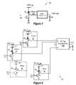
- FIG. 4is a simplified schematic block diagram of an exemplary power amplification system that connects a plurality of different power amplifiers 402 , 412 , 422 , 432 through a multi-tap transformer 444 to a shared output load 446 .
- Each power amplifiere.g., 402
- Each power amplifierincludes a power supply V DD (e.g., 403 ), an inductor (e.g., 404 ) and an input transistor (e.g., 406 ).
- the input transistor (e.g., 406 )is operably coupled to receive a power amplifier input voltage V IN (e.g., 405 ), which may be provided for amplification (e.g., from the up-conversion module 82 in FIG. 2 ).
- the input transistor 406amplifies the input voltage V IN 405 based on the transistor gain and the load provided by the inductor 404 .
- the inductor 404is coupled to the drain of each input transistor (e.g., at node V DRAIN 407 ), which in turn is connected to a tap of a multi-tap transformer 444 .
- a separate inductor 404may not be required because the transformer winding can be used to replace the inductor and/or the transformer section can be driven by non-inductively loaded power amplifiers.
- the multi-tap transformer 444may be constructed as described herein with reference to FIGS.
- each input voltage V IN 405 , 415 , 425 , 435is coupled to efficiently amplify the input power through a dedicated load impedance Rnetwork of the transformer 444 , depending on which terminal tap(s) of the secondary winding of transformer 444 is coupled to the amplifier.
- each one of the N tapsmay be stimulated by N power amplifiers (e.g., 402 , 412 , 422 , 432 ).
- N power amplifierse.g., 402 , 412 , 422 , 432 .
- any one of the N tap/power amplifier pairscan be activated to deliver power into the secondary side of the transformer 444 , which is then coupled to the load resistance 446 through the primary side of the transformer 444 .
- any one of the N pairscan be optimized to be highly efficient. Since each of the N taps presents a different impedance, N different power levels can efficiently be delivered to the load 446 .
- various combinations of any of the N pairscan be turned on to deliver different combinations of powers to the primary side of the transformer 444 , thereby providing at least N different power levels. Since each power amplifier is optimized for efficiency, any of the N power levels is efficient.
- FIG. 5illustrates a simplified schematic block diagram of a plurality of differential power amplifiers 502 , 522 , 532 , 534 that are connected through a multi-tap transformer 542 to a shared output load 562 (e.g., antenna 86 in FIG. 2 ), where each differential power amplifier (e.g., 502 ) includes an inductor 504 , input transistors T 3 and T 4 and current control transistors T 1 and T 2 .
- the input transistors T 3 and T 4are operably coupled to receive a differential input 506 (e.g., from the up-conversion module 82 in FIG. 2 ), which may be provided for power amplification (e.g., to generate differential outbound RF signal 98 from the power amplifier module 84 in FIG.
- the input transistors T 3 and T 4amplify the differential input 506 based on their respective gains and the load provided by the differential inductor 504 .
- the inductor 504may be implemented as separate inductor elements or may be constructed in accordance with the teachings of U.S. patent application Ser. No. 10/200,802 entitled “On-Chip Differential Inductor and Applications Thereof,” (now U.S. Pat. No. 7,039,381), which is hereby incorporated fully by reference as if set forth herein.
- one or more of the N tapsmay be stimulated by N power amplifiers (e.g., 502 , 522 , 532 , 534 ) to deliver power into the secondary side of the transformer 542 , which is then coupled to the load resistance 562 through the primary side of the transformer 542 .
- N power amplifierse.g., 502 , 522 , 532 , 534
- FIG. 6is a schematic diagram of an on-chip multi-tap transformer 600 that is operably coupled to convert a plurality of single ended input signals 613 , 615 , 617 , 619 into a single ended output signal 601 .
- the transformer 600includes a primary winding 603 and a secondary winding 604 .
- the secondary winding 604includes a first portion and a second portion, each of which includes two nodes and a tap.
- a ground node 610 of the secondary winding 604is coupled to a reference potential (e.g., AC ground).
- the input voltages from the single ended power amplifiersare operably coupled to the remaining nodes and taps of the first and second portions of the secondary winding 604 , thereby providing input voltages with reference the input ground 610 .
- the taps 613 , 617may be implemented symmetrically with reference to the nodes 610 , 615 , 619 , though asymmetric configurations may also be used to couple one or more input voltages 613 , 615 , 617 , 619 to the output signal 601 .
- the turn ratio between the any input voltage on the secondary winding and the primary winding 603controls the load impedance provided by the transformer 600 .
- the primary winding 603may consist of two turns while the secondary winding 604 consists of nine turns, though those of ordinary skill in the art will appreciate that other combinations of turn ratios may be used.
- the transformer 600may be used for a single power amplifier by having the other inputs disabled during the required operations, in other applications, more than one power amplifier may be applied as inputs to the transformer 600 to thereby efficiently combine the power amplification operations.
- FIG. 7illustrates a schematic diagram of an alternate on-chip multiple tap transformer balun 700 that is operably coupled to convert one or more differential input signals 706 or 708 into a single ended output signal 703 .
- the transformer 700includes a primary winding 703 and a secondary winding 704 such that a first differential input signal 708 or second differential input signal 706 may be coupled to the secondary winding 704 .
- the primary winding 703produces a single ended output signal 703 corresponding to either the first differential input signal 708 or the second differential input signal 706 .
- the secondary winding 704includes a first and second portion, each having a first node, a second node, and a tap.
- the second nodes 714 of the respective portions of the secondary winding 704are operably coupled to the AC ground reference potential, and the first nodes 710 , 718 of the respective portions are coupled to receive the first differential input signal 708 .
- the taps 712 , 716 of each portion of the secondary winding 704are operably coupled to receive the second differential input signal 706 .
- the first and second differential input signals 706 , 708may be used individually or simultaneously to provide inputs to the transformer 700 .
- the resulting single ended output signal 703will represent a mixing of the first and second differential input signals 706 , 708 .
- FIGS. 8-10illustrate a physical embodiment of the multi-tap transformers 600 or 700 of FIG. 6 and 7 , which may be used to couple multiple power amplifiers to an output load.
- the depicted transformercan be used to couple up to two differential power amplifiers, or up to four single ended power amplifiers, to an output load.
- FIG. 8illustrates the top view of the secondary winding 800 .
- the secondary winding 800includes a first node of a second portion 808 , a tap of the first portion 806 , bridges 805 , a tap of the second portion 804 , a first node of the first portion 802 , and a coupling to a reference potential 810 .
- the number of turns for the secondary winding 800may vary from one to multiple turns.
- the secondary winding 800may be fabricated using a metallization layer of the integrated circuit having low resistivity. Typically, for a CMOS process, this particular metallization layer is the top metal layer.
- FIG. 8illustrates a top view of a multi-tap secondary winding 800 of a physical embodiment for a multi-tap differential inductor.
- the first windingcorresponds to the first portion (e.g., starting at node 802 ) of the secondary winding 800 and the second winding corresponds to the second portion (e.g., starting at node 808 ).
- the secondary winding 800may include shunt windings on different layers. By using shunt windings, the series resistance of the inductor decreases, thereby increasing the quality factor of the inductor.
- FIG. 9illustrates a cross sectional view of multi-tap transformers 600 or 700 to include an upper dielectric layer 844 , a middle dielectric layer 846 , and a lower dielectric layer 848 .
- the upper dielectric layer 844supports a metallization layer that is used to fabricate the secondary winding 800 .
- the middle dielectric layer 846supports the bridges 842 and the coupling to the reference potential 810 .
- the lower dielectric layer 848supports the primary winding 850 .
- FIG. 10illustrates a bottom view of multi-tap transformers 600 or 700 and illustrates the geometric shape of an embodiment of the primary winding 850 .
- the primary winding 850is shown to include one turn, but may include multiple turns, depending on the desired turn ratio for multi-tap transformers 600 or 700 .
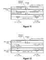
- FIG. 11illustrates an alternate cross sectional view of a multi-tap transformer in accordance with the present invention where the secondary winding 1100 includes a shunt winding 1156 .
- the secondary winding 1100includes a shunt winding 1156 .
- five support dielectric layers 1144 , 1146 , 1148 , 1152 and 1154are illustrated.
- the secondary winding 1100is supported by the first dielectric layer 1144
- the shunt winding 1156is supported by the third dielectric layer 1148
- the corresponding bridges 1105 and the reference potential couplings 1110are supported by the second and fourth dielectric layers 1152 , 1146
- the primary winding 1150is supported by the fifth dielectric layer 1154 .
- the shunt winding 1156is coupled in parallel with the secondary winding 1100 to reduce the resistivity of the secondary winding 1100 .
- FIG. 12illustrates an alternate cross sectional view of a multi-tap transformer that includes the primary winding 1250 including one or more shunt windings.
- the primary windingincludes two shunt windings 1262 , 1264 .
- the additional shunt windingsare supported by dielectric layers 1258 and 1260 .
- the secondary winding 1200 and the primary winding 1250may include shunt windings.
- a transformer incorporating a combination of FIGS. 11 and 12may also be implemented.
- FIG. 13illustrates an alternate embodiment of the secondary winding 1300 or the multi-tap differential inductor that may be used to receive multiple input voltage signals.
- the geometric shapecorresponds to a rectangular octagonal shape.
- the particular length and width of the rectangular octagonal shapeis based on a balancing of the inductance value, the turn ratio, the quality factor and capacitance of the windings.
- the second winding 1300includes a first portion and a second portion, where each portion has one node and two taps.
- the secondary windingincludes a first node of the first portion 1302 , a first tap of the second portion 1304 , bridges 1306 , a first tap of the first portion 1308 , a first node of the second portion 1310 , a second tap of the second portion 1312 , a coupling to a reference potential 1314 , and a second tap of the first portion 1316 .
- the bridges 1306are used to couple the various windings together and to maintain symmetry of the second winding 1300 .
- the present inventionprovides an on-chip multi-tap inductor that may be used for the N-tap transformer illustrated in FIGS. 4-5 .
- the inductor 1300includes a first interwound winding (beginning at node 1302 ) and a second interwound winding (beginning at node 1310 ).
- the second nodes 1314 of the respective portions of the secondary winding 1300are operably coupled to the AC ground reference potential, and the first nodes 1302 , 1310 of the respective portions are coupled to receive a first differential input signal, the first taps 1304 , 1308 of the first and second portion of the secondary winding 1300 may be operably coupled to receive a second differential input signal, and the second taps 1312 , 1316 of the first and second portion may be operably coupled to receive a third differential signal.
- FIG. 14illustrates a cross sectional view of a single layered multi-tap transformer inductor 1400 .
- the primary and secondary interwound windings 1400 and 1402are fabricated from a metallization layer lying on a first dielectric layer 1404 .
- the first dielectric layer 1404may be comprised of silicon oxide, or any other insulating integrated circuit material.
- the bridges 1408are fabricated on a metallization layer that lies on the second dielectric layer 1406 .
- the primary interwound winding 1400 and secondary interwound winding 1402are interwound with respect to each other. This provides the desired magnetic coupling while minimizing the capacitance.
- the number of windings, the width of the windings, and the shape of the windingsdepend on the operating parameters under which the multi-tap transformer inductor will be required to perform. For example, with an operating frequency for the multi-tap transformer inductor that is less than half of the self-resonating frequency of the inductor, the acceptable capacitance and desired inductance may be derived.
- the quality factor(which typically improves the circuit performance with higher values) is based on the resistivity of the windings 1400 , 1402 . As such, the trace thickness for the windings 1400 , 1402 is determined to provide the desired series resistance, and the windings are typically placed on the metal layer having the lowest resistivity. In this manner, the quality factor of the multi-tap transformer inductor may be optimized.
- FIG. 15illustrates a cross sectional view of an alternate multi-tap transformer inductor that includes shunt windings 1512 and 1514 .
- the primary and secondary interwound windings 1500 and 1502are on the first dielectric layer 1504 .
- the corresponding bridges 1518 for the primary and secondary interwound windings 1500 and 1502are on the second dielectric layer 1506 .
- Two additional dielectric layers 1508 and 1510may be used to implement the alternate multi-tap transformer for this embodiment.
- Dielectric layer 1508supports the metallization layer that is used to fabricate a first shunt winding 1512 that is coupled in parallel with the primary interwound winding 1500 .
- the dielectric layer 1508supports the second shunt winding 1514 that is coupled in parallel with the secondary interwound winding 1502 .
- Dielectric layer 1510supports the bridges 1516 used to fabricate the first and second shunt windings 1512 and 1514 .
- the quality factormay be further enhanced since the series resistance of the primary and secondary interwound windings 1500 and 1502 are reduced.
- additional shunt windingsmay be coupled in parallel with the primary and secondary interwound windings 1500 and 1502 to further increase the quality factor by reducing the series resistance.
Landscapes
- Engineering & Computer Science (AREA)
- Power Engineering (AREA)
- Amplifiers (AREA)
Abstract
Description
where Rnetwork is the load impedance presented by the
Psupply=VDD*I,
then the efficiency is given by the ratio of the input power delivered into the
Since Vdrain is the product of the AC drain current, Idrain, and Rnetwork, the Efficiency expression can be rewritten as:
Claims (20)
Priority Applications (1)
| Application Number | Priority Date | Filing Date | Title |
|---|---|---|---|
| US11/553,190US7365602B2 (en) | 2004-10-28 | 2006-10-26 | Multilevel power amplifier architecture using multi-tap transformer |
Applications Claiming Priority (2)
| Application Number | Priority Date | Filing Date | Title |
|---|---|---|---|
| US10/975,240US7129784B2 (en) | 2004-10-28 | 2004-10-28 | Multilevel power amplifier architecture using multi-tap transformer |
| US11/553,190US7365602B2 (en) | 2004-10-28 | 2006-10-26 | Multilevel power amplifier architecture using multi-tap transformer |
Related Parent Applications (1)
| Application Number | Title | Priority Date | Filing Date |
|---|---|---|---|
| US10/975,240ContinuationUS7129784B2 (en) | 2004-10-28 | 2004-10-28 | Multilevel power amplifier architecture using multi-tap transformer |
Publications (2)
| Publication Number | Publication Date |
|---|---|
| US20070069818A1 US20070069818A1 (en) | 2007-03-29 |
| US7365602B2true US7365602B2 (en) | 2008-04-29 |
Family
ID=36261124
Family Applications (2)
| Application Number | Title | Priority Date | Filing Date |
|---|---|---|---|
| US10/975,240Expired - Fee RelatedUS7129784B2 (en) | 2004-10-28 | 2004-10-28 | Multilevel power amplifier architecture using multi-tap transformer |
| US11/553,190Expired - LifetimeUS7365602B2 (en) | 2004-10-28 | 2006-10-26 | Multilevel power amplifier architecture using multi-tap transformer |
Family Applications Before (1)
| Application Number | Title | Priority Date | Filing Date |
|---|---|---|---|
| US10/975,240Expired - Fee RelatedUS7129784B2 (en) | 2004-10-28 | 2004-10-28 | Multilevel power amplifier architecture using multi-tap transformer |
Country Status (1)
| Country | Link |
|---|---|
| US (2) | US7129784B2 (en) |
Cited By (20)
| Publication number | Priority date | Publication date | Assignee | Title |
|---|---|---|---|---|
| US20070279099A1 (en)* | 2006-05-30 | 2007-12-06 | Jennic Limited | Transceiver and method of operating an electrical circuit |
| US20090184786A1 (en)* | 2008-01-03 | 2009-07-23 | Chang-Ho Lee | Multi-segment primary and multi-turn secondary transformer for power amplifier systems |
| US20090273397A1 (en)* | 2008-05-05 | 2009-11-05 | Bockelman David E | Controlling power with an output network |
| US20090309662A1 (en)* | 2008-06-12 | 2009-12-17 | Ki Seok Yang | Systems and Methods for Power Amplifier with Integrated Passive Device |
| US20100052782A1 (en)* | 2008-08-28 | 2010-03-04 | Industrial Technology Research Institute | Transformer and structure thereof and power amplifier |
| US20100148866A1 (en)* | 2007-01-10 | 2010-06-17 | Samsung Electro-Mechanics Company | Systems and Methods for Power Amplifiers with Voltage Boosting Multi-Primary Transformers |
| US20100164621A1 (en)* | 2008-12-30 | 2010-07-01 | Vishnu Srinivasan | Output gain stage for a power amplifier |
| US20100225400A1 (en)* | 2009-03-03 | 2010-09-09 | Ahmadreza Rofougaran | Method and system for on-chip impedance control to impedance match a configurable front end |
| US7812701B2 (en) | 2008-01-08 | 2010-10-12 | Samsung Electro-Mechanics | Compact multiple transformers |
| WO2010126478A1 (en)* | 2009-04-27 | 2010-11-04 | Hewlett-Packard Development Company, L.P. | Electric power conversion system having an adaptable transformer turns ratio for improved efficiency |
| US20110043316A1 (en)* | 2008-01-08 | 2011-02-24 | Ki Seok Yang | Overlapping compact multiple transformers |
| US20110221522A1 (en)* | 2010-03-12 | 2011-09-15 | Samsung Electro-Mechanics Company, Ltd. | Sharing of inductor interstage matching in parallel amplification system for wireless communication systems |
| US20120056680A1 (en)* | 2009-10-08 | 2012-03-08 | Qualcomm Incorporated | Three Dimensional Inductor, Transformer and Radio Frequency Amplifier |
| KR101124055B1 (en) | 2008-11-25 | 2012-03-23 | 조지아 테크 리서치 코오포레이션 | Power amplifier with discrete power control |
| US8198968B2 (en) | 2010-09-30 | 2012-06-12 | Fujitsu Semiconductor Limited | System and method for multiple band transmission |
| US8232857B1 (en) | 2009-04-15 | 2012-07-31 | Triquint Semiconductor, Inc. | Flux-coupled transformer for power amplifier output matching |
| US20130127528A1 (en)* | 2011-11-21 | 2013-05-23 | Electronics And Telecommunications Research Institute | Power amplifier and amplification method thereof |
| US8786381B2 (en) | 2010-06-28 | 2014-07-22 | Avago Technologies General Ip (Singapore) Pte. Ltd. | Transformer structures for a power amplifier (PA) |
| US20180115198A1 (en)* | 2016-10-20 | 2018-04-26 | Taiwan Semiconductor Manufacturing Co., Ltd. | Wireless transmitter with switchable mode |
| US20220416751A1 (en)* | 2021-06-24 | 2022-12-29 | Intel Corporation | Impedance matching circuit and an impedance matching element |
Families Citing this family (111)
| Publication number | Priority date | Publication date | Assignee | Title |
|---|---|---|---|---|
| KR100852315B1 (en) | 2000-10-10 | 2008-08-14 | 캘리포니아 인스티튜트 오브 테크놀로지 | Power amplifiers and methods thereof, and inductors |
| US6856199B2 (en)* | 2000-10-10 | 2005-02-15 | California Institute Of Technology | Reconfigurable distributed active transformers |
| TWI326967B (en) | 2002-03-11 | 2010-07-01 | California Inst Of Techn | Differential amplifier |
| US7369096B2 (en)* | 2003-10-10 | 2008-05-06 | Broadcom Corporation | Impedance matched passive radio frequency transmit/receive switch |
| US7095283B2 (en)* | 2003-10-28 | 2006-08-22 | Axiom Microdevices, Inc. | Supply circuit for power amplifier drivers |
| US7372336B2 (en)* | 2004-12-31 | 2008-05-13 | Samsung Electronics Co., Ltd. | Small-sized on-chip CMOS power amplifier having improved efficiency |
| US7483727B2 (en)* | 2005-04-04 | 2009-01-27 | Research In Motion Limited | Mobile wireless communications device having improved antenna impedance match and antenna gain from RF energy |
| US7605673B2 (en)* | 2006-06-02 | 2009-10-20 | Coherent, Inc. | Transformer for impedance-matching power output of RF amplifier to gas-laser discharge |
| US8963369B2 (en)* | 2007-12-04 | 2015-02-24 | Solaredge Technologies Ltd. | Distributed power harvesting systems using DC power sources |
| US11735910B2 (en) | 2006-12-06 | 2023-08-22 | Solaredge Technologies Ltd. | Distributed power system using direct current power sources |
| US11687112B2 (en) | 2006-12-06 | 2023-06-27 | Solaredge Technologies Ltd. | Distributed power harvesting systems using DC power sources |
| US8473250B2 (en) | 2006-12-06 | 2013-06-25 | Solaredge, Ltd. | Monitoring of distributed power harvesting systems using DC power sources |
| US8618692B2 (en) | 2007-12-04 | 2013-12-31 | Solaredge Technologies Ltd. | Distributed power system using direct current power sources |
| US9088178B2 (en) | 2006-12-06 | 2015-07-21 | Solaredge Technologies Ltd | Distributed power harvesting systems using DC power sources |
| US12316274B2 (en) | 2006-12-06 | 2025-05-27 | Solaredge Technologies Ltd. | Pairing of components in a direct current distributed power generation system |
| US8947194B2 (en) | 2009-05-26 | 2015-02-03 | Solaredge Technologies Ltd. | Theft detection and prevention in a power generation system |
| US8319471B2 (en) | 2006-12-06 | 2012-11-27 | Solaredge, Ltd. | Battery power delivery module |
| US8013472B2 (en) | 2006-12-06 | 2011-09-06 | Solaredge, Ltd. | Method for distributed power harvesting using DC power sources |
| US8816535B2 (en) | 2007-10-10 | 2014-08-26 | Solaredge Technologies, Ltd. | System and method for protection during inverter shutdown in distributed power installations |
| US11855231B2 (en)* | 2006-12-06 | 2023-12-26 | Solaredge Technologies Ltd. | Distributed power harvesting systems using DC power sources |
| US11569659B2 (en) | 2006-12-06 | 2023-01-31 | Solaredge Technologies Ltd. | Distributed power harvesting systems using DC power sources |
| US11888387B2 (en) | 2006-12-06 | 2024-01-30 | Solaredge Technologies Ltd. | Safety mechanisms, wake up and shutdown methods in distributed power installations |
| US7596364B2 (en)* | 2006-12-08 | 2009-09-29 | Telefonaktiebolaget L M Ericsson (Publ) | Merged low-noise amplifier and balun |
| US7710197B2 (en) | 2007-07-11 | 2010-05-04 | Axiom Microdevices, Inc. | Low offset envelope detector and method of use |
| CN105244905B (en) | 2007-12-05 | 2019-05-21 | 太阳能安吉有限公司 | Release mechanism in distributed power device is waken up and method for closing |
| US7911388B2 (en)* | 2007-12-12 | 2011-03-22 | Broadcom Corporation | Method and system for configurable antenna in an integrated circuit package |
| US8144674B2 (en)* | 2008-03-27 | 2012-03-27 | Broadcom Corporation | Method and system for inter-PCB communications with wireline control |
| US8270912B2 (en)* | 2007-12-12 | 2012-09-18 | Broadcom Corporation | Method and system for a transformer in an integrated circuit package |
| US8494030B2 (en)* | 2008-06-19 | 2013-07-23 | Broadcom Corporation | Method and system for 60 GHz wireless clock distribution |
| US8855093B2 (en)* | 2007-12-12 | 2014-10-07 | Broadcom Corporation | Method and system for chip-to-chip communications with wireline control |
| US7880677B2 (en)* | 2007-12-12 | 2011-02-01 | Broadcom Corporation | Method and system for a phased array antenna embedded in an integrated circuit package |
| US20090153250A1 (en)* | 2007-12-12 | 2009-06-18 | Ahmadreza Rofougaran | Method and system for scaling supply, device size, and load of a power amplifier |
| US8583197B2 (en)* | 2007-12-12 | 2013-11-12 | Broadcom Corporation | Method and system for sharing antennas for high frequency and low frequency applications |
| US8115567B2 (en)* | 2007-12-13 | 2012-02-14 | Broadcom Corporation | Method and system for matching networks embedded in an integrated circuit package |
| US8134425B2 (en)* | 2007-12-13 | 2012-03-13 | Broadcom Corporation | Method and system for filters embedded in an integrated circuit package |
| US7863998B2 (en)* | 2008-02-25 | 2011-01-04 | Broadcom Corporation | Method and system for processing signals via directional couplers embedded in an integrated circuit package |
| US7859359B2 (en)* | 2008-02-25 | 2010-12-28 | Broadcom Corporation | Method and system for a balun embedded in an integrated circuit package |
| US20090219908A1 (en)* | 2008-02-29 | 2009-09-03 | Ahmadreza Rofougaran | Method and system for processing signals via diplexers embedded in an integrated circuit package |
| US8994488B2 (en) | 2008-03-12 | 2015-03-31 | Mediatek Inc. | Transformer power splitter having primary winding conductors magnetically coupled to secondary winding conductors and configured in topology including series connection and parallel connection |
| US7777570B2 (en)* | 2008-03-12 | 2010-08-17 | Mediatek Inc. | Transformer power combiner having secondary winding conductors magnetically coupled to primary winding conductors and configured in topology including series connection and parallel connection |
| US8072287B2 (en)* | 2008-03-27 | 2011-12-06 | Broadcom Corporation | Method and system for configurable differential or single-ended signaling in an integrated circuit |
| US7982555B2 (en) | 2008-03-28 | 2011-07-19 | Broadcom Corporation | Method and system for processing signals via power splitters embedded in an integrated circuit package |
| US8198714B2 (en)* | 2008-03-28 | 2012-06-12 | Broadcom Corporation | Method and system for configuring a transformer embedded in a multi-layer integrated circuit (IC) package |
| US8344808B2 (en) | 2008-03-31 | 2013-01-01 | Javelin Semiconductor, Inc. | Non-linear capacitance compensation |
| US8787850B2 (en) | 2008-03-31 | 2014-07-22 | Avago Technologies General Ip (Singapore) Pte. Ltd. | Compensating for non-linear capacitance effects in a power amplifier |
| US7872528B2 (en)* | 2008-04-10 | 2011-01-18 | Javelin Semiconductor, Inc. | Providing pre-distortion to an input signal |
| EP2294669B8 (en) | 2008-05-05 | 2016-12-07 | Solaredge Technologies Ltd. | Direct current power combiner |
| US8116676B2 (en)* | 2008-05-07 | 2012-02-14 | Broadcom Corporation | Method and system for inter IC communications utilizing a spatial multi-link repeater |
| US8212541B2 (en) | 2008-05-08 | 2012-07-03 | Massachusetts Institute Of Technology | Power converter with capacitive energy transfer and fast dynamic response |
| US8483627B2 (en)* | 2008-05-09 | 2013-07-09 | Texas Instruments Incorporated | Circuits, processes, devices and systems for full integration of RF front end module including RF power amplifier |
| US8160520B2 (en)* | 2008-05-09 | 2012-04-17 | Javelin Semiconductor, Inc. | Supply control for multiple power modes of a power amplifier |
| KR101003587B1 (en)* | 2008-10-13 | 2010-12-22 | 삼성전기주식회사 | CMCOS RF IC |
| EP3447910B1 (en) | 2008-11-11 | 2020-12-16 | Massachusetts Institute Of Technology | An asymmetric multilevel outphasing architecture for rf amplifiers |
| US8665052B2 (en)* | 2009-08-12 | 2014-03-04 | Mediatek Inc. | Transformer-based circuit with compact and/or symmetrical layout design |
| US12418177B2 (en) | 2009-10-24 | 2025-09-16 | Solaredge Technologies Ltd. | Distributed power system using direct current power sources |
| US8116700B2 (en)* | 2009-11-16 | 2012-02-14 | Javelin Semiconductor, Inc. | Reducing common mode effects in an output stage |
| GB2485527B (en) | 2010-11-09 | 2012-12-19 | Solaredge Technologies Ltd | Arc detection and prevention in a power generation system |
| US10673229B2 (en) | 2010-11-09 | 2020-06-02 | Solaredge Technologies Ltd. | Arc detection and prevention in a power generation system |
| KR101904364B1 (en)* | 2010-12-23 | 2018-11-30 | 마벨 월드 트레이드 리미티드 | Figure 8 balun |
| US10389235B2 (en) | 2011-05-05 | 2019-08-20 | Psemi Corporation | Power converter |
| GB2483317B (en) | 2011-01-12 | 2012-08-22 | Solaredge Technologies Ltd | Serially connected inverters |
| EP4318909A3 (en) | 2011-05-05 | 2024-03-06 | PSEMI Corporation | Dc-dc converter with modular stages |
| US10680515B2 (en) | 2011-05-05 | 2020-06-09 | Psemi Corporation | Power converters with modular stages |
| US9882471B2 (en) | 2011-05-05 | 2018-01-30 | Peregrine Semiconductor Corporation | DC-DC converter with modular stages |
| US8743553B2 (en) | 2011-10-18 | 2014-06-03 | Arctic Sand Technologies, Inc. | Power converters with integrated capacitors |
| US8723491B2 (en) | 2011-12-19 | 2014-05-13 | Arctic Sand Technologies, Inc. | Control of power converters with capacitive energy transfer |
| GB2498365A (en) | 2012-01-11 | 2013-07-17 | Solaredge Technologies Ltd | Photovoltaic module |
| US9853565B2 (en) | 2012-01-30 | 2017-12-26 | Solaredge Technologies Ltd. | Maximized power in a photovoltaic distributed power system |
| GB2498790A (en) | 2012-01-30 | 2013-07-31 | Solaredge Technologies Ltd | Maximising power in a photovoltaic distributed power system |
| GB2498791A (en) | 2012-01-30 | 2013-07-31 | Solaredge Technologies Ltd | Photovoltaic panel circuitry |
| US9065386B2 (en) | 2012-02-29 | 2015-06-23 | Avago Technologies General Ip (Singapore) Pte. Ltd. | Low voltage operation for a power amplifier |
| US9172338B2 (en)* | 2012-06-01 | 2015-10-27 | Intel Corporation | Transformer-based RF power amplifier |
| US8928405B2 (en)* | 2012-09-10 | 2015-01-06 | Cambridge Silicon Radio Limited | Power amplification circuits |
| US8779881B2 (en)* | 2012-09-21 | 2014-07-15 | Cambridge Silicon Radio Limited | Varying inductance |
| US8824978B2 (en) | 2012-10-30 | 2014-09-02 | Eta Devices, Inc. | RF amplifier architecture and related techniques |
| US9537456B2 (en) | 2012-10-30 | 2017-01-03 | Eta Devices, Inc. | Asymmetric multilevel backoff amplifier with radio-frequency splitter |
| US8829993B2 (en) | 2012-10-30 | 2014-09-09 | Eta Devices, Inc. | Linearization circuits and methods for multilevel power amplifier systems |
| US9166536B2 (en) | 2012-10-30 | 2015-10-20 | Eta Devices, Inc. | Transmitter architecture and related methods |
| DE102013101768A1 (en)* | 2013-02-22 | 2014-08-28 | Intel Mobile Communications GmbH | Transformer and electrical circuit |
| US9548619B2 (en) | 2013-03-14 | 2017-01-17 | Solaredge Technologies Ltd. | Method and apparatus for storing and depleting energy |
| US8724353B1 (en) | 2013-03-15 | 2014-05-13 | Arctic Sand Technologies, Inc. | Efficient gate drivers for switched capacitor converters |
| US20140273825A1 (en)* | 2013-03-15 | 2014-09-18 | Infineon Technologies Ag | Semiconductor Chip Configuration with a Coupler |
| US8619445B1 (en) | 2013-03-15 | 2013-12-31 | Arctic Sand Technologies, Inc. | Protection of switched capacitor power converter |
| WO2014168911A1 (en) | 2013-04-09 | 2014-10-16 | Massachusetts Institute Of Technology | Power conservation with high power factor |
| US9825545B2 (en) | 2013-10-29 | 2017-11-21 | Massachusetts Institute Of Technology | Switched-capacitor split drive transformer power conversion circuit |
| JP6353053B2 (en) | 2014-02-03 | 2018-07-04 | ジョンソン コントロールズ テクノロジー カンパニーJohnson Controls Technology Company | Multi-pulse constant voltage transformer for variable speed drive in cooling device applications |
| US9654066B2 (en)* | 2014-04-03 | 2017-05-16 | Marvell World Trade Ltd. | Common-source power amplifiers |
| US9520906B2 (en) | 2014-06-25 | 2016-12-13 | Qualcomm Incorporated | Switched capacitor transmitter circuits and methods |
| US10075064B2 (en) | 2014-07-03 | 2018-09-11 | Massachusetts Institute Of Technology | High-frequency, high density power factor correction conversion for universal input grid interface |
| US9768731B2 (en) | 2014-07-23 | 2017-09-19 | Eta Devices, Inc. | Linearity and noise improvement for multilevel power amplifier systems using multi-pulse drain transitions |
| JP2018506842A (en)* | 2014-12-15 | 2018-03-08 | シーメンス アクチエンゲゼルシヤフトSiemens Aktiengesellschaft | Fluid cooled balun transformer |
| US9979421B2 (en) | 2015-03-02 | 2018-05-22 | Eta Devices, Inc. | Digital pre-distortion (DPD) training and calibration system and related techniques |
| WO2016149063A1 (en) | 2015-03-13 | 2016-09-22 | Arctic Sand Technologies, Inc. | Dc-dc transformer with inductor for the facilitation of adiabatic inter-capacitor charge transport |
| US9425737B1 (en)* | 2015-03-16 | 2016-08-23 | Futurewei Technologies, Inc. | Tapped inductor voltage controlled oscillator |
| WO2017007991A1 (en) | 2015-07-08 | 2017-01-12 | Arctic Sand Technologies, Inc. | Switched-capacitor power converters |
| US12057807B2 (en) | 2016-04-05 | 2024-08-06 | Solaredge Technologies Ltd. | Chain of power devices |
| US11018623B2 (en) | 2016-04-05 | 2021-05-25 | Solaredge Technologies Ltd. | Safety switch for photovoltaic systems |
| US11177663B2 (en) | 2016-04-05 | 2021-11-16 | Solaredge Technologies Ltd. | Chain of power devices |
| US9793942B1 (en)* | 2016-06-20 | 2017-10-17 | Ubilite, Inc. | Systems and methods for a switchless radio front end |
| US9859357B1 (en)* | 2016-07-14 | 2018-01-02 | International Business Machines Corporation | Magnetic inductor stacks with multilayer isolation layers |
| US10283249B2 (en) | 2016-09-30 | 2019-05-07 | International Business Machines Corporation | Method for fabricating a magnetic material stack |
| US10236838B2 (en) | 2017-02-03 | 2019-03-19 | Qualcomm Incorporated | Multi-power amplification |
| US10284166B2 (en) | 2017-06-27 | 2019-05-07 | Intel Corporation | Transmitter matching network using a transformer |
| US11694836B2 (en) | 2018-03-30 | 2023-07-04 | Intel Corporation | On-chip multi-layer transformer and inductor |
| CN109245733A (en)* | 2018-09-04 | 2019-01-18 | 中国商用飞机有限责任公司北京民用飞机技术研究中心 | A kind of linear power amplifier of multivoltage output |
| US11195655B2 (en) | 2018-10-24 | 2021-12-07 | Analog Devices International Unlimited Company | Segmented winding techniques for a coupled inductor circuit |
| US10917132B1 (en)* | 2019-07-10 | 2021-02-09 | Rockwell Collins, Inc. | Switchless transceiver integrated programmable differential topology |
| US11430600B2 (en) | 2020-04-17 | 2022-08-30 | Analog Devices International Unlimited Company | Segmented winding center-tap techniques for a coupled inductor circuit |
| US11574766B2 (en) | 2020-04-17 | 2023-02-07 | Analog Devices International Unlimited Company | Techniques for a coupled inductor circuit |
| CN112910425B (en)* | 2021-01-28 | 2022-07-19 | 武汉大学 | High-efficiency and large-capacity piecewise linear power amplifier based on multi-tap transformer |
| CN117097278B (en)* | 2021-02-08 | 2025-01-28 | 锐石创芯(深圳)科技股份有限公司 | Push-pull power amplifier system and RF front-end module |
Citations (8)
| Publication number | Priority date | Publication date | Assignee | Title |
|---|---|---|---|---|
| US5570062A (en) | 1994-10-12 | 1996-10-29 | Ericsson Ge Mobile Communications Inc. | AM-FM transmitter power amplifier using class-BC |
| US20030194976A1 (en) | 2002-04-15 | 2003-10-16 | Bhatti Iqbal S. | On-chip impedance matching power amplifier and radio applications thereof |
| US20030197575A1 (en) | 2002-04-23 | 2003-10-23 | Rozieh Rofougaran | Integrated circuit low noise amplifier and applications thereof |
| US20030197656A1 (en) | 2002-04-23 | 2003-10-23 | Yang Hung Yu David | Printed antenna and applications thereof |
| US20040018823A1 (en) | 2002-07-23 | 2004-01-29 | Yang Hung Yu | On-chip differential inductor and applications thereof |
| US20040017278A1 (en) | 2002-07-23 | 2004-01-29 | Castaneda Jesus A. | On-chip multiple tap transformer and inductor |
| US6882263B2 (en) | 2002-01-23 | 2005-04-19 | Broadcom, Corp. | On-chip transformer balun |
| US7091791B1 (en)* | 2004-07-23 | 2006-08-15 | Atheros Communications, Inc. | Transformer implementation using bonding wires |
- 2004
- 2004-10-28USUS10/975,240patent/US7129784B2/ennot_activeExpired - Fee Related
- 2006
- 2006-10-26USUS11/553,190patent/US7365602B2/ennot_activeExpired - Lifetime
Patent Citations (10)
| Publication number | Priority date | Publication date | Assignee | Title |
|---|---|---|---|---|
| US5570062A (en) | 1994-10-12 | 1996-10-29 | Ericsson Ge Mobile Communications Inc. | AM-FM transmitter power amplifier using class-BC |
| US6882263B2 (en) | 2002-01-23 | 2005-04-19 | Broadcom, Corp. | On-chip transformer balun |
| US20030194976A1 (en) | 2002-04-15 | 2003-10-16 | Bhatti Iqbal S. | On-chip impedance matching power amplifier and radio applications thereof |
| US20030197575A1 (en) | 2002-04-23 | 2003-10-23 | Rozieh Rofougaran | Integrated circuit low noise amplifier and applications thereof |
| US20030197656A1 (en) | 2002-04-23 | 2003-10-23 | Yang Hung Yu David | Printed antenna and applications thereof |
| US20040018823A1 (en) | 2002-07-23 | 2004-01-29 | Yang Hung Yu | On-chip differential inductor and applications thereof |
| US20040017278A1 (en) | 2002-07-23 | 2004-01-29 | Castaneda Jesus A. | On-chip multiple tap transformer and inductor |
| US6707367B2 (en) | 2002-07-23 | 2004-03-16 | Broadcom, Corp. | On-chip multiple tap transformer and inductor |
| US7039381B2 (en) | 2002-07-23 | 2006-05-02 | Broadcom Corporation | On-chip differential inductor and applications thereof |
| US7091791B1 (en)* | 2004-07-23 | 2006-08-15 | Atheros Communications, Inc. | Transformer implementation using bonding wires |
Cited By (38)
| Publication number | Priority date | Publication date | Assignee | Title |
|---|---|---|---|---|
| US7787830B2 (en)* | 2006-05-30 | 2010-08-31 | Jennic Limited | Transceiver and method of operating an electrical circuit |
| US20070279099A1 (en)* | 2006-05-30 | 2007-12-06 | Jennic Limited | Transceiver and method of operating an electrical circuit |
| US7880547B2 (en) | 2007-01-10 | 2011-02-01 | Samsung Electro-Mechanics | Systems and methods for power amplifiers with voltage boosting multi-primary transformers |
| US20100148866A1 (en)* | 2007-01-10 | 2010-06-17 | Samsung Electro-Mechanics Company | Systems and Methods for Power Amplifiers with Voltage Boosting Multi-Primary Transformers |
| US20090184786A1 (en)* | 2008-01-03 | 2009-07-23 | Chang-Ho Lee | Multi-segment primary and multi-turn secondary transformer for power amplifier systems |
| US7936215B2 (en) | 2008-01-03 | 2011-05-03 | Samsung-Electro Mechanics | Multi-segment primary and multi-turn secondary transformer for power amplifier systems |
| US8044759B2 (en) | 2008-01-08 | 2011-10-25 | Samsung Electro-Mechanics | Overlapping compact multiple transformers |
| US7812701B2 (en) | 2008-01-08 | 2010-10-12 | Samsung Electro-Mechanics | Compact multiple transformers |
| US20110043316A1 (en)* | 2008-01-08 | 2011-02-24 | Ki Seok Yang | Overlapping compact multiple transformers |
| US7728661B2 (en)* | 2008-05-05 | 2010-06-01 | Javelin Semiconductor, Inc. | Controlling power with an output network |
| US20090273397A1 (en)* | 2008-05-05 | 2009-11-05 | Bockelman David E | Controlling power with an output network |
| US20090309662A1 (en)* | 2008-06-12 | 2009-12-17 | Ki Seok Yang | Systems and Methods for Power Amplifier with Integrated Passive Device |
| US7746174B2 (en)* | 2008-06-12 | 2010-06-29 | Samsung Electro-Mechanics Company, Ltd. | Systems and methods for power amplifier with integrated passive device |
| US20100052782A1 (en)* | 2008-08-28 | 2010-03-04 | Industrial Technology Research Institute | Transformer and structure thereof and power amplifier |
| US7812671B2 (en) | 2008-08-28 | 2010-10-12 | Industrial Technology Research Institute | Transformer and structure thereof and power amplifier |
| KR101124055B1 (en) | 2008-11-25 | 2012-03-23 | 조지아 테크 리서치 코오포레이션 | Power amplifier with discrete power control |
| US7768350B2 (en) | 2008-12-30 | 2010-08-03 | Javelin Semiconductor, Inc. | Output gain stage for a power amplifier |
| US20100164621A1 (en)* | 2008-12-30 | 2010-07-01 | Vishnu Srinivasan | Output gain stage for a power amplifier |
| US8666340B2 (en)* | 2009-03-03 | 2014-03-04 | Broadcom Corporation | Method and system for on-chip impedance control to impedance match a configurable front end |
| US20100225400A1 (en)* | 2009-03-03 | 2010-09-09 | Ahmadreza Rofougaran | Method and system for on-chip impedance control to impedance match a configurable front end |
| US8232857B1 (en) | 2009-04-15 | 2012-07-31 | Triquint Semiconductor, Inc. | Flux-coupled transformer for power amplifier output matching |
| WO2010126478A1 (en)* | 2009-04-27 | 2010-11-04 | Hewlett-Packard Development Company, L.P. | Electric power conversion system having an adaptable transformer turns ratio for improved efficiency |
| CN102414973B (en)* | 2009-04-27 | 2015-07-01 | 惠普开发有限公司 | Electric power conversion system with adaptable transformer turns ratio for improved efficiency |
| CN102414973A (en)* | 2009-04-27 | 2012-04-11 | 惠普开发有限公司 | Electric power conversion system having an adaptable transformer turns ratio for improved efficiency |
| US8817491B2 (en) | 2009-04-27 | 2014-08-26 | Hewlett-Packard Development Company, L.P. | Electric power conversion system having an adaptable transformer turns ratio for improved efficiency |
| GB2481752A (en)* | 2009-04-27 | 2012-01-04 | Hewlett Packard Development Co | Electric power conversion system having an adaptable transformer turns ratio for improved efficiency |
| GB2481752B (en)* | 2009-04-27 | 2013-12-04 | Hewlett Packard Development Co | Electric power conversion system having an adaptable transformer turns ratio for improved efficiency |
| US20120056680A1 (en)* | 2009-10-08 | 2012-03-08 | Qualcomm Incorporated | Three Dimensional Inductor, Transformer and Radio Frequency Amplifier |
| US8508301B2 (en)* | 2009-10-08 | 2013-08-13 | Qualcomm Incorporated | Three dimensional inductor, transformer and radio frequency amplifier |
| US20110221522A1 (en)* | 2010-03-12 | 2011-09-15 | Samsung Electro-Mechanics Company, Ltd. | Sharing of inductor interstage matching in parallel amplification system for wireless communication systems |
| US8125276B2 (en) | 2010-03-12 | 2012-02-28 | Samsung Electro-Mechanics | Sharing of inductor interstage matching in parallel amplification system for wireless communication systems |
| US8786381B2 (en) | 2010-06-28 | 2014-07-22 | Avago Technologies General Ip (Singapore) Pte. Ltd. | Transformer structures for a power amplifier (PA) |
| US8198968B2 (en) | 2010-09-30 | 2012-06-12 | Fujitsu Semiconductor Limited | System and method for multiple band transmission |
| US20130127528A1 (en)* | 2011-11-21 | 2013-05-23 | Electronics And Telecommunications Research Institute | Power amplifier and amplification method thereof |
| US9118282B2 (en)* | 2011-11-21 | 2015-08-25 | Electronics And Telecommunications Research Institute | Power amplifier and amplification method thereof |
| US20180115198A1 (en)* | 2016-10-20 | 2018-04-26 | Taiwan Semiconductor Manufacturing Co., Ltd. | Wireless transmitter with switchable mode |
| US10491046B2 (en)* | 2016-10-20 | 2019-11-26 | Taiwan Semiconductor Manufacturing Co., Ltd. | Wireless transmitter with switchable mode |
| US20220416751A1 (en)* | 2021-06-24 | 2022-12-29 | Intel Corporation | Impedance matching circuit and an impedance matching element |
Also Published As
| Publication number | Publication date |
|---|---|
| US20060091958A1 (en) | 2006-05-04 |
| US20070069818A1 (en) | 2007-03-29 |
| US7129784B2 (en) | 2006-10-31 |
Similar Documents
| Publication | Publication Date | Title |
|---|---|---|
| US7365602B2 (en) | Multilevel power amplifier architecture using multi-tap transformer | |
| US6919858B2 (en) | RF antenna coupling structure | |
| US7538741B2 (en) | Impedance matched passive radio frequency transmit/receive switch | |
| US7796970B2 (en) | Integrated low noise amplifier | |
| US8380153B2 (en) | Radio front end and applications thereof | |
| US7209727B2 (en) | Integrated circuit radio front-end architecture and applications thereof | |
| US7728661B2 (en) | Controlling power with an output network | |
| US6882228B2 (en) | Radio frequency integrated circuit having an antenna diversity structure | |
| US7269391B2 (en) | Tunable transceiver front end | |
| US6819914B2 (en) | Differential mixer injection with optional step gain control | |
| US7039381B2 (en) | On-chip differential inductor and applications thereof | |
| US7129803B2 (en) | Tuned transformer balun circuit and applications thereof | |
| US20100041361A1 (en) | Method and system for a single-ended input low noise amplifier with differential output | |
| JP2013535885A (en) | Broadband balun with a single primary winding and multiple secondary windings | |
| US7079816B2 (en) | On chip diversity antenna switch | |
| JP2012502512A (en) | Passive transmitter configuration with switchable output for wireless applications | |
| US9490865B2 (en) | Transceiver suitable for multiple power level operation and method therefor | |
| US7184735B2 (en) | Radio frequency integrated circuit having symmetrical differential layout | |
| US20050088262A1 (en) | Tuning RF circuits using switched inductors | |
| US7071799B2 (en) | High performance switch for switched inductor tuned RF circuit | |
| US20060066431A1 (en) | Adjustable differential inductor | |
| Tang et al. | CMOS 2.4-GHz receiver front end with area-efficient inductors and digitally calibrated 90/spl deg/delay network |
Legal Events
| Date | Code | Title | Description |
|---|---|---|---|
| STCF | Information on status: patent grant | Free format text:PATENTED CASE | |
| FPAY | Fee payment | Year of fee payment:4 | |
| FPAY | Fee payment | Year of fee payment:8 | |
| AS | Assignment | Owner name:BANK OF AMERICA, N.A., AS COLLATERAL AGENT, NORTH CAROLINA Free format text:PATENT SECURITY AGREEMENT;ASSIGNOR:BROADCOM CORPORATION;REEL/FRAME:037806/0001 Effective date:20160201 Owner name:BANK OF AMERICA, N.A., AS COLLATERAL AGENT, NORTH Free format text:PATENT SECURITY AGREEMENT;ASSIGNOR:BROADCOM CORPORATION;REEL/FRAME:037806/0001 Effective date:20160201 | |
| AS | Assignment | Owner name:AVAGO TECHNOLOGIES GENERAL IP (SINGAPORE) PTE. LTD., SINGAPORE Free format text:ASSIGNMENT OF ASSIGNORS INTEREST;ASSIGNOR:BROADCOM CORPORATION;REEL/FRAME:041706/0001 Effective date:20170120 Owner name:AVAGO TECHNOLOGIES GENERAL IP (SINGAPORE) PTE. LTD Free format text:ASSIGNMENT OF ASSIGNORS INTEREST;ASSIGNOR:BROADCOM CORPORATION;REEL/FRAME:041706/0001 Effective date:20170120 | |
| AS | Assignment | Owner name:BROADCOM CORPORATION, CALIFORNIA Free format text:TERMINATION AND RELEASE OF SECURITY INTEREST IN PATENTS;ASSIGNOR:BANK OF AMERICA, N.A., AS COLLATERAL AGENT;REEL/FRAME:041712/0001 Effective date:20170119 | |
| AS | Assignment | Owner name:AVAGO TECHNOLOGIES INTERNATIONAL SALES PTE. LIMITE Free format text:MERGER;ASSIGNOR:AVAGO TECHNOLOGIES GENERAL IP (SINGAPORE) PTE. LTD.;REEL/FRAME:047195/0658 Effective date:20180509 | |
| AS | Assignment | Owner name:AVAGO TECHNOLOGIES INTERNATIONAL SALES PTE. LIMITE Free format text:CORRECTIVE ASSIGNMENT TO CORRECT THE EFFECTIVE DATE OF MERGER PREVIOUSLY RECORDED ON REEL 047195 FRAME 0658. ASSIGNOR(S) HEREBY CONFIRMS THE THE EFFECTIVE DATE IS 09/05/2018;ASSIGNOR:AVAGO TECHNOLOGIES GENERAL IP (SINGAPORE) PTE. LTD.;REEL/FRAME:047357/0302 Effective date:20180905 | |
| AS | Assignment | Owner name:AVAGO TECHNOLOGIES INTERNATIONAL SALES PTE. LIMITE Free format text:CORRECTIVE ASSIGNMENT TO CORRECT THE ERROR IN RECORDING THE MERGER PREVIOUSLY RECORDED AT REEL: 047357 FRAME: 0302. ASSIGNOR(S) HEREBY CONFIRMS THE ASSIGNMENT;ASSIGNOR:AVAGO TECHNOLOGIES GENERAL IP (SINGAPORE) PTE. LTD.;REEL/FRAME:048674/0834 Effective date:20180905 | |
| MAFP | Maintenance fee payment | Free format text:PAYMENT OF MAINTENANCE FEE, 12TH YEAR, LARGE ENTITY (ORIGINAL EVENT CODE: M1553); ENTITY STATUS OF PATENT OWNER: LARGE ENTITY Year of fee payment:12 |