US7365411B2 - Resistance variable memory with temperature tolerant materials - Google Patents
Resistance variable memory with temperature tolerant materialsDownload PDFInfo
- Publication number
- US7365411B2 US7365411B2US10/916,423US91642304AUS7365411B2US 7365411 B2US7365411 B2US 7365411B2US 91642304 AUS91642304 AUS 91642304AUS 7365411 B2US7365411 B2US 7365411B2
- Authority
- US
- United States
- Prior art keywords
- layer
- metal
- electrode
- chalcogenide
- memory device
- Prior art date
- Legal status (The legal status is an assumption and is not a legal conclusion. Google has not performed a legal analysis and makes no representation as to the accuracy of the status listed.)
- Expired - Lifetime, expires
Links
- 239000000463materialSubstances0.000titleclaimsdescription20
- 239000011521glassSubstances0.000claimsdescription34
- 229910052751metalInorganic materials0.000claimsdescription21
- 239000002184metalSubstances0.000claimsdescription21
- 229910052709silverInorganic materials0.000claimsdescription14
- 239000004332silverSubstances0.000claimsdescription13
- 230000037361pathwayEffects0.000claimsdescription9
- KDSXXMBJKHQCAA-UHFFFAOYSA-Ndisilver;selenium(2-)Chemical compound[Se-2].[Ag+].[Ag+]KDSXXMBJKHQCAA-UHFFFAOYSA-N0.000claimsdescription6
- MFIWAIVSOUGHLI-UHFFFAOYSA-Nselenium;tinChemical compound[Sn]=[Se]MFIWAIVSOUGHLI-UHFFFAOYSA-N0.000claimsdescription4
- 239000005387chalcogenide glassSubstances0.000abstractdescription20
- 238000000034methodMethods0.000abstractdescription15
- OQRNKLRIQBVZHK-UHFFFAOYSA-NselanylideneantimonyChemical compound[Sb]=[Se]OQRNKLRIQBVZHK-UHFFFAOYSA-N0.000abstractdescription5
- 239000010410layerSubstances0.000description96
- 239000011669seleniumSubstances0.000description18
- 239000000758substrateSubstances0.000description15
- BQCADISMDOOEFD-UHFFFAOYSA-NSilverChemical compound[Ag]BQCADISMDOOEFD-UHFFFAOYSA-N0.000description12
- 239000004065semiconductorSubstances0.000description10
- 239000004020conductorSubstances0.000description8
- 150000004770chalcogenidesChemical class0.000description7
- 230000003750conditioning effectEffects0.000description7
- WFKWXMTUELFFGS-UHFFFAOYSA-NtungstenChemical compound[W]WFKWXMTUELFFGS-UHFFFAOYSA-N0.000description7
- 229910052721tungstenInorganic materials0.000description7
- 239000010937tungstenSubstances0.000description7
- PXHVJJICTQNCMI-UHFFFAOYSA-NNickelChemical compound[Ni]PXHVJJICTQNCMI-UHFFFAOYSA-N0.000description5
- 229910052787antimonyInorganic materials0.000description5
- WATWJIUSRGPENY-UHFFFAOYSA-Nantimony atomChemical compound[Sb]WATWJIUSRGPENY-UHFFFAOYSA-N0.000description5
- 230000015572biosynthetic processEffects0.000description5
- BASFCYQUMIYNBI-UHFFFAOYSA-NplatinumChemical compound[Pt]BASFCYQUMIYNBI-UHFFFAOYSA-N0.000description5
- 238000012545processingMethods0.000description5
- 229910052711seleniumInorganic materials0.000description5
- QIHHYQWNYKOHEV-UHFFFAOYSA-N4-tert-butyl-3-nitrobenzoic acidChemical compoundCC(C)(C)C1=CC=C(C(O)=O)C=C1[N+]([O-])=OQIHHYQWNYKOHEV-UHFFFAOYSA-N0.000description4
- BUGBHKTXTAQXES-UHFFFAOYSA-NSeleniumChemical compound[Se]BUGBHKTXTAQXES-UHFFFAOYSA-N0.000description4
- 229910052581Si3N4Inorganic materials0.000description4
- 238000000151depositionMethods0.000description4
- HQVNEWCFYHHQES-UHFFFAOYSA-Nsilicon nitrideChemical compoundN12[Si]34N5[Si]62N3[Si]51N64HQVNEWCFYHHQES-UHFFFAOYSA-N0.000description4
- 238000004544sputter depositionMethods0.000description4
- -1Ag2Se)Chemical compound0.000description3
- 229910052798chalcogenInorganic materials0.000description3
- 238000005229chemical vapour depositionMethods0.000description3
- 239000010949copperSubstances0.000description3
- 238000005530etchingMethods0.000description3
- 239000010931goldSubstances0.000description3
- 150000002500ionsChemical class0.000description3
- 150000002739metalsChemical class0.000description3
- 229910052760oxygenInorganic materials0.000description3
- 229910052717sulfurInorganic materials0.000description3
- 229910052714telluriumInorganic materials0.000description3
- NINIDFKCEFEMDL-UHFFFAOYSA-NSulfurChemical compound[S]NINIDFKCEFEMDL-UHFFFAOYSA-N0.000description2
- 239000000956alloySubstances0.000description2
- 229910045601alloyInorganic materials0.000description2
- 229910052782aluminiumInorganic materials0.000description2
- XAGFODPZIPBFFR-UHFFFAOYSA-NaluminiumChemical compound[Al]XAGFODPZIPBFFR-UHFFFAOYSA-N0.000description2
- QVGXLLKOCUKJST-UHFFFAOYSA-Natomic oxygenChemical compound[O]QVGXLLKOCUKJST-UHFFFAOYSA-N0.000description2
- 230000004888barrier functionEffects0.000description2
- 150000001787chalcogensChemical class0.000description2
- 229910052802copperInorganic materials0.000description2
- 230000006870functionEffects0.000description2
- PCHJSUWPFVWCPO-UHFFFAOYSA-NgoldChemical compound[Au]PCHJSUWPFVWCPO-UHFFFAOYSA-N0.000description2
- 229910052737goldInorganic materials0.000description2
- 239000012212insulatorSubstances0.000description2
- 238000004519manufacturing processMethods0.000description2
- 230000006386memory functionEffects0.000description2
- 230000005012migrationEffects0.000description2
- 238000013508migrationMethods0.000description2
- 229910052759nickelInorganic materials0.000description2
- 239000001301oxygenSubstances0.000description2
- 229920002120photoresistant polymerPolymers0.000description2
- 229910052697platinumInorganic materials0.000description2
- 229910052699poloniumInorganic materials0.000description2
- 229910021420polycrystalline siliconInorganic materials0.000description2
- 229920000642polymerPolymers0.000description2
- 229920005591polysiliconPolymers0.000description2
- 239000002356single layerSubstances0.000description2
- 239000011593sulfurSubstances0.000description2
- PORWMNRCUJJQNO-UHFFFAOYSA-Ntellurium atomChemical compound[Te]PORWMNRCUJJQNO-UHFFFAOYSA-N0.000description2
- 239000010936titaniumSubstances0.000description2
- RYGMFSIKBFXOCR-UHFFFAOYSA-NCopperChemical compound[Cu]RYGMFSIKBFXOCR-UHFFFAOYSA-N0.000description1
- XUIMIQQOPSSXEZ-UHFFFAOYSA-NSiliconChemical compound[Si]XUIMIQQOPSSXEZ-UHFFFAOYSA-N0.000description1
- ATJFFYVFTNAWJD-UHFFFAOYSA-NTinChemical compound[Sn]ATJFFYVFTNAWJD-UHFFFAOYSA-N0.000description1
- RTAQQCXQSZGOHL-UHFFFAOYSA-NTitaniumChemical compound[Ti]RTAQQCXQSZGOHL-UHFFFAOYSA-N0.000description1
- NRTOMJZYCJJWKI-UHFFFAOYSA-NTitanium nitrideChemical compound[Ti]#NNRTOMJZYCJJWKI-UHFFFAOYSA-N0.000description1
- 210000004027cellAnatomy0.000description1
- 210000005056cell bodyAnatomy0.000description1
- 239000000919ceramicSubstances0.000description1
- 230000008859changeEffects0.000description1
- 238000010549co-EvaporationMethods0.000description1
- 150000001875compoundsChemical class0.000description1
- 230000006735deficitEffects0.000description1
- 230000008021depositionEffects0.000description1
- 238000001704evaporationMethods0.000description1
- 230000008020evaporationEffects0.000description1
- 229910052732germaniumInorganic materials0.000description1
- GNPVGFCGXDBREM-UHFFFAOYSA-Ngermanium atomChemical compound[Ge]GNPVGFCGXDBREM-UHFFFAOYSA-N0.000description1
- 239000011810insulating materialSubstances0.000description1
- 238000002955isolationMethods0.000description1
- 229910021645metal ionInorganic materials0.000description1
- 239000000203mixtureSubstances0.000description1
- 230000004048modificationEffects0.000description1
- 238000012986modificationMethods0.000description1
- 150000004767nitridesChemical class0.000description1
- 238000000059patterningMethods0.000description1
- 230000000737periodic effectEffects0.000description1
- 230000002093peripheral effectEffects0.000description1
- 238000005240physical vapour depositionMethods0.000description1
- 238000000623plasma-assisted chemical vapour depositionMethods0.000description1
- 238000007747platingMethods0.000description1
- 238000005498polishingMethods0.000description1
- HZEBHPIOVYHPMT-UHFFFAOYSA-Npolonium atomChemical compound[Po]HZEBHPIOVYHPMT-UHFFFAOYSA-N0.000description1
- 230000008569processEffects0.000description1
- 238000011160researchMethods0.000description1
- 229910052594sapphireInorganic materials0.000description1
- 239000010980sapphireSubstances0.000description1
- 229910052710siliconInorganic materials0.000description1
- 239000010703siliconSubstances0.000description1
- 239000000126substanceSubstances0.000description1
- 238000006467substitution reactionMethods0.000description1
- UQMCSSLUTFUDSN-UHFFFAOYSA-NsulfanylidenegermaneChemical compound[GeH2]=SUQMCSSLUTFUDSN-UHFFFAOYSA-N0.000description1
- PGWMQVQLSMAHHO-UHFFFAOYSA-NsulfanylidenesilverChemical compound[Ag]=SPGWMQVQLSMAHHO-UHFFFAOYSA-N0.000description1
- 230000003319supportive effectEffects0.000description1
- 229910052715tantalumInorganic materials0.000description1
- GUVRBAGPIYLISA-UHFFFAOYSA-Ntantalum atomChemical compound[Ta]GUVRBAGPIYLISA-UHFFFAOYSA-N0.000description1
- 229910052719titaniumInorganic materials0.000description1
Images


Classifications
- H—ELECTRICITY
- H10—SEMICONDUCTOR DEVICES; ELECTRIC SOLID-STATE DEVICES NOT OTHERWISE PROVIDED FOR
- H10N—ELECTRIC SOLID-STATE DEVICES NOT OTHERWISE PROVIDED FOR
- H10N70/00—Solid-state devices having no potential barriers, and specially adapted for rectifying, amplifying, oscillating or switching
- H10N70/20—Multistable switching devices, e.g. memristors
- H10N70/24—Multistable switching devices, e.g. memristors based on migration or redistribution of ionic species, e.g. anions, vacancies
- H10N70/245—Multistable switching devices, e.g. memristors based on migration or redistribution of ionic species, e.g. anions, vacancies the species being metal cations, e.g. programmable metallization cells
- H—ELECTRICITY
- H10—SEMICONDUCTOR DEVICES; ELECTRIC SOLID-STATE DEVICES NOT OTHERWISE PROVIDED FOR
- H10N—ELECTRIC SOLID-STATE DEVICES NOT OTHERWISE PROVIDED FOR
- H10N70/00—Solid-state devices having no potential barriers, and specially adapted for rectifying, amplifying, oscillating or switching
- H10N70/011—Manufacture or treatment of multistable switching devices
- H10N70/061—Shaping switching materials
- H10N70/063—Shaping switching materials by etching of pre-deposited switching material layers, e.g. lithography
- H—ELECTRICITY
- H10—SEMICONDUCTOR DEVICES; ELECTRIC SOLID-STATE DEVICES NOT OTHERWISE PROVIDED FOR
- H10N—ELECTRIC SOLID-STATE DEVICES NOT OTHERWISE PROVIDED FOR
- H10N70/00—Solid-state devices having no potential barriers, and specially adapted for rectifying, amplifying, oscillating or switching
- H10N70/011—Manufacture or treatment of multistable switching devices
- H10N70/021—Formation of switching materials, e.g. deposition of layers
- H10N70/026—Formation of switching materials, e.g. deposition of layers by physical vapor deposition, e.g. sputtering
- H—ELECTRICITY
- H10—SEMICONDUCTOR DEVICES; ELECTRIC SOLID-STATE DEVICES NOT OTHERWISE PROVIDED FOR
- H10N—ELECTRIC SOLID-STATE DEVICES NOT OTHERWISE PROVIDED FOR
- H10N70/00—Solid-state devices having no potential barriers, and specially adapted for rectifying, amplifying, oscillating or switching
- H10N70/801—Constructional details of multistable switching devices
- H10N70/821—Device geometry
- H10N70/826—Device geometry adapted for essentially vertical current flow, e.g. sandwich or pillar type devices
- H—ELECTRICITY
- H10—SEMICONDUCTOR DEVICES; ELECTRIC SOLID-STATE DEVICES NOT OTHERWISE PROVIDED FOR
- H10N—ELECTRIC SOLID-STATE DEVICES NOT OTHERWISE PROVIDED FOR
- H10N70/00—Solid-state devices having no potential barriers, and specially adapted for rectifying, amplifying, oscillating or switching
- H10N70/801—Constructional details of multistable switching devices
- H10N70/881—Switching materials
- H10N70/882—Compounds of sulfur, selenium or tellurium, e.g. chalcogenides
- H10N70/8825—Selenides, e.g. GeSe
- Y—GENERAL TAGGING OF NEW TECHNOLOGICAL DEVELOPMENTS; GENERAL TAGGING OF CROSS-SECTIONAL TECHNOLOGIES SPANNING OVER SEVERAL SECTIONS OF THE IPC; TECHNICAL SUBJECTS COVERED BY FORMER USPC CROSS-REFERENCE ART COLLECTIONS [XRACs] AND DIGESTS
- Y10—TECHNICAL SUBJECTS COVERED BY FORMER USPC
- Y10S—TECHNICAL SUBJECTS COVERED BY FORMER USPC CROSS-REFERENCE ART COLLECTIONS [XRACs] AND DIGESTS
- Y10S438/00—Semiconductor device manufacturing: process
- Y10S438/90—Bulk effect device making
Definitions
- the inventionrelates to the field of random access memory (RAM) devices formed using a resistance variable material and a metal-chalcogenide material.
- Resistance variable memory elementswhich include Programmable Conductive Random Access Memory (PCRAM) elements, have been investigated for suitability as semi-volatile and non-volatile random access memory devices.
- PCRAMProgrammable Conductive Random Access Memory
- the conductivity/resistance of a chalcogenide glass backbonecan be programmed to stable lower conductivity (i.e., higher resistance) and higher conductivity (i.e., lower resistance) states.
- An unprogrammed PCRAM deviceis normally in a lower conductivity, higher resistance state.
- a conditioning operationforms a conducting channel of a metal-chalcogenide in the PCRAM device, which supports a conductive pathway for altering the conductivity/resistivity state of the device.
- a write operationwill program the PCRAM device to a higher conductivity state, in which metal ions accumulate along the conducting channel(s).
- the PCRAM devicemay be read by applying a voltage of a lesser magnitude than required to program it; the current or resistance across the memory device is sensed as higher or lower to define the logic “one” and “zero” states.
- the PCRAMmay be erased by applying a reverse voltage (opposite bias) relative to the write voltage, which disrupts the conductive pathway, but typically leaves the conducting channel intact. In this way, such a device can function as a variable resistance memory having at least two conductivity states, which can define two respective logic states, i.e., at least a bit of data.
- One exemplary PCRAM deviceuses a germanium selenide (i.e., Ge x Se 100-x ) chalcogenide glass as a backbone.
- the germanium selenide glasshas, in the prior art, incorporated silver (Ag) by (photo or thermal) doping or co-deposition.
- exemplary PCRAM deviceshave done away with such doping or co-deposition by incorporating a metal-chalcogenide material as a layer of silver selenide (e.g., Ag 2 Se), silver sulfide (AgS), or tin selenide (SnSe) in combination with a metal layer, proximate a chalcogenide glass layer, which during conditioning of the PCRAM provides material to form a conducting channel and a conductive pathway in the glass backbone.
- a metal-chalcogenide materialas a layer of silver selenide (e.g., Ag 2 Se), silver sulfide (AgS), or tin selenide (SnSe) in combination with a metal layer, proximate a chalcogenide glass layer, which during conditioning of the PCRAM provides material to form a conducting channel and a conductive pathway in the glass backbone.
- a glass backbone of Ge 40 Se 60with an accompanying metal-chalcogenide (e.g., typically silver selenide) layer, enables a conducting channel to be formed in the glass backbone during conditioning, which can thereafter more easily be programmed to form a conductive pathway.
- the metal-chalcogenideis incorporated into chalcogenide glass layer at the conditioning step.
- the conditioning stepcomprises applying a potential (e.
- metal-chalcogenideis incorporated into the chalcogenide glass layer, thereby forming a conducting channel within the chalcogenide glass layer.
- Movement of metal (e.g., typically silver) ions into or out of the conducting channel during subsequent writing and erasingforms or dissolves a conductive pathway along the conducting channel, which causes a detectible conductivity (or resistance) change across the memory device.
- Exemplary embodiments of the inventionprovide a method of forming and a structure, in which a PCRAM memory device has a chalcogenide glass backbone layer, preferably comprising antimony selenide having a stoichiometric formula of about Sb 2 Se 3 , and a metal-chalcogenide layer, which cooperates with the backbone layer.
- a chalcogenide glass backbone layerpreferably comprising antimony selenide having a stoichiometric formula of about Sb 2 Se 3
- a metal-chalcogenide layerwhich cooperates with the backbone layer.
- FIGS. 1 and 2show exemplary embodiments of memory devices in accordance with the invention.
- FIGS. 3-6illustrate exemplary sequential stages of processing during the fabrication of an embodiment of the invention as shown in FIG. 1 .
- FIG. 7shows an exemplary processor-based system incorporating memory devices in accordance with and embodiment the invention.
- substrateused in the following description may include any supporting structure including, but not limited to, a semiconductor substrate that has a substrate surface.
- a semiconductor substrateshould be understood to include silicon-on-insulator (SOI), silicon-on-sapphire (SOS), doped and undoped semiconductors, epitaxial layers of silicon supported by a base semiconductor foundation, and other semiconductor structures.
- SOIsilicon-on-insulator
- SOSsilicon-on-sapphire
- doped and undoped semiconductorssilicon-on-insulator
- epitaxial layers of silicon supported by a base semiconductor foundationand other semiconductor structures.
- the substrateneed not be semiconductor-based, but may be any support structure suitable for supporting an integrated circuit, including, but not limited to, metals, alloys, glasses, polymers, ceramics, and any other supportive materials as is known in the art.
- chalcogenide glassis intended to include glasses that comprise at least one non-chalcogenide component selected from Groups 3-15 and at least one chalcogenide component from Group 16 of the periodic table.
- Group 16elementse.g., sulfur (S), selenium (Se), tellurium (Te), polonium (Po), and oxygen (O) are also referred to as chalcogens.
- metal-chalcogenideis intended to include various alloys, compounds, and mixtures of metals and chalcogens (e.g., O, S, Se, Te, and Po), including some species which have a slight excess or deficit of metal.
- chalcogense.g., O, S, Se, Te, and Po
- tin selenidea species of metal-chalcogenide
- silver selenideanother species of metal-chalcogenide
- the inventionis not limited to a particular stoichiometric ratio between the metal and chalcogenide components.
- the metal-chalcogenidepreferably incorporates the same chalcogenide component as in the chalcogenide glass; however, this is not a requirement and it is possible for a different chalcogenide component to be used in the metal-chalcogenide.
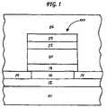
- FIG. 1shows an exemplary embodiment of a memory device 100 constructed in accordance with the invention.
- the device 100 shown in FIG. 1is supported by a substrate 10 .
- a conductive address line 12which serves as an interconnect for the device 100 shown and a plurality of other similar devices of a portion of a memory array, of which the shown device 100 is a part.
- an optional insulating layer(not shown) between the substrate 10 and address line 12 , and this may be preferred if the substrate 10 is semiconductor-based.
- the conductive address line 12can be any material known in the art as being useful for providing an interconnect line, such as doped polysilicon, silver (Ag), gold (Au), copper (Cu), tungsten (W), nickel (Ni), aluminum (Al), platinum (Pt), titanium (Ti), and other materials.
- a first electrode 16which is defined within an insulating layer 14 , which is also over the address line 12 .
- This electrode 16can be any conductive material that will not migrate into chalcogenide glass, but is preferably tungsten (W).
- the insulating layer 14should not allow the migration of metal (e.g., silver) ions and can be an insulating nitride, such as silicon nitride (Si 3 N 4 ), a low dielectric constant material, an insulating glass, or an insulating polymer, but is not limited to such materials.
- metale.g., silver
- a memory elementi.e., the portion of the memory device 100 which stores information, is provided over the first electrode 16 .
- a layer of chalcogenide glass 18preferably antimony selenide having a stoichiometric formula of about Sb 2 Se 3 (referred to hereafter as Sb 2 Se 3 glass), is provided as a glass backbone over the first electrode 16 .
- the layer of Sb 2 Se 3 glass 18is preferably between about 100 ⁇ and about 1000 ⁇ thick, most preferably about 150 ⁇ thick.
- Layer 18need not be a single layer of Sb 2 Se 3 glass, but may also be comprised of multiple sub-layers of Sb 2 Se 3 glass having the same or different stoichiometries. This layer of Sb 2 Se 3 glass 18 is in electrical contact with the underlying electrode 16 .
- metal-chalcogenide 20preferably silver selenide (e.g., Ag 2 Se). It is also possible that other metals may be substituted for silver, such as tin, and other chalcogenide materials may be substituted for selenium, such as sulfur, oxygen, or tellurium.
- the metal-chalcogenide layer 20is preferably about 470 ⁇ thick; however, its thickness depends, in part, on the thickness of the underlying Sb 2 Se 3 glass layer 18 .
- the ratio of the thickness of the metal-chalcogenide layer 20 to that of the underlying Sb 2 Se 3 glass layer 18should be between about 5:1 and about 1:1, more preferably about 2.5:1.
- a metal layer 22is provided over the metal-chalcogenide layer 20 , with silver (Ag) or antimony (Sb) being preferred as the metal.
- This metal layer 22should be about 200 ⁇ thick.
- This metal layer 22assists the switching operation of the memory device 100 .
- a second electrode 24Over the metal layer 22 is a second electrode 24 .
- the second electrode 24can be made of the same material as the first electrode 16 , but is not required to be so. In the exemplary embodiment shown in FIG. 1 , the second electrode 24 is preferably tungsten (W).
- the device(s)may be isolated by an insulating layer 26 .
- Sb 2 Se 3 layere.g., glass backbone layer 18
- PCRAM devicesusing a germanium selenide glass backbone.
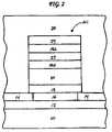
- FIG. 2shows another exemplary embodiment of a memory device 101 constructed in accordance with the invention.
- Memory device 101has many similarities to memory device 100 of FIG. 1 and layers designated with like reference numbers, such as Sb 2 Se 3 glass layer 18 , are preferably the same materials and have the same thicknesses as those described in relation to the embodiment shown in FIG. 1 .
- the primary difference between device 100 and device 101is the addition to device 101 of optional chalcogenide glass layers 18 a and 18 b.
- the optional chalcogenide glass layer 18 ais formed over the metal-chalcogenide layer 20 , is preferably Ge 40 Se 60 , and is preferably about 150 ⁇ thick. Over this optional chalcogenide glass layer 18 a is a metal layer 22 , which is preferably silver (Ag) or antimony (Sb) and is preferably about 200 ⁇ thick. Over the metal layer 22 is another optional chalcogenide glass layer 18 b , which is preferably Ge 40 Se 60 and is preferably about 100 ⁇ thick. The optional chalcogenide glass layer 18 b provides an adhesion layer for subsequent electrode formation. As with layer 18 of FIG. 1 , layers 18 a and 18 b are not necessarily a single layer, but may be comprised of multiple sub-layers.
- the optional chalcogenide layers 18 a and 18 bmay be the same as or different chalcogenide glasses from the antimony selenide glass layer 18 or each other.
- Other chalcogenide glasses that may be useful for this purposeinclude, but are not limited to, germanium sulfide (GeS), and combination of germanium (Ge), silver (Ag), and selenium (Se).
- a second electrode 24which may be any conductive material, except those that will migrate into the stack and alter memory operation (e.g., Cu or Ag), as discussed above for the preceding embodiments.
- the second electrode 24is tungsten (W).
- the above-discussed embodimentsare exemplary embodiments of the invention utilizing a Sb 2 Se 3 glass backbone layer (e.g., layer 18 ); however, other exemplary embodiments may be used which combine the first electrode layer 16 and address line layer 12 .
- Another exemplary embodimentmay use blanket layers (e.g., layers 16 , 18 , 20 , and 22 of FIG. 1 ) of the memory cell body, where the memory cell is defined locally by the position of the second electrode 24 over the substrate 10 .
- Another exemplary embodimentmay form the memory device within a via. Additional layers, such as barrier layers or alloy-controlling layers, not specifically disclosed in the embodiments shown and discussed above, may be added to the devices in accordance with the invention without departing from the scope thereof.
- FIGS. 3-6illustrate a cross-sectional view of a wafer during the fabrication of a memory device 100 incorporating a Sb 2 Se 3 glass backbone layer, as shown by FIG. 1 .
- FIGS. 3-6illustrate a cross-sectional view of a wafer during the fabrication of a memory device 100 incorporating a Sb 2 Se 3 glass backbone layer, as shown by FIG. 1 .
- the processing steps shown in FIGS. 3-6most specifically refer to memory device 100 of FIG. 1
- the methods and techniques discussedmay also be used to fabricate memory device 101 of FIG. 2 , or other embodiments, as would be understood by a person of ordinary skill in the art based on a reading of this specification.
- a substrate 10is provided.
- the substrate 10can be semiconductor-based or another material useful as a supporting structure as is known in the art.
- an optional insulating layer(not shown) may be formed over the substrate 10 ; the optional insulating layer may be silicon nitride or other insulating materials used in the art.
- a conductive address line 12is formed by depositing a conductive material, such as doped polysilicon, aluminum, platinum, silver, gold, nickel, but preferably tungsten, patterning one or more conductive lines, for instance with photolithographic techniques, and etching to define the address line 12 .
- the conductive materialmaybe deposited by any technique known in the art, such as sputtering, chemical vapor deposition, plasma enhanced chemical vapor deposition, evaporation, or plating.
- an insulating layer 14over the address line 12 is formed an insulating layer 14 .
- This layer 14can be silicon nitride, a low dielectric constant material, or many other insulators known in the art that do not allow metal (e.g., silver) ion migration, and may be deposited by any method known in the art.
- An opening 14 a in the insulating layeris made, for instance by photolithographic and etching techniques, thereby exposing a portion of the underlying address line 12 .
- a conductive materialpreferably tungsten (W).
- a chemical mechanical polishing stepmay then be utilized to remove the conductive material from over the insulating layer 14 , to leave it as a first electrode 16 over the address line 12 , and planarize the wafer.
- FIG. 4shows the cross-section of the wafer of FIG. 3 at a subsequent stage of processing.
- a series of layers making up the memory device 100( FIG. 1 ) are blanket-deposited over the wafer.
- a Sb 2 Se 3 glass layer 18is formed to a preferred thickness of about 150 ⁇ over the first electrode 16 and insulating layer 14 .
- Deposition of this Sb 2 Se 3 glass layer 18may be accomplished by any suitable method, such as evaporative techniques or chemical vapor deposition; however, the preferred technique utilizes either sputtering from an antimony selenide target having the desired stoichiometry or co-sputtering antimony and selenium in the appropriate ratios.
- a metal-chalcogenide layer 20is formed over the Sb 2 Se 3 glass layer 18 .
- the metal-chalcogenide layer 20is preferably silver selenide (e.g., Ag 2 Se), but may be other metal-chalcogenide combinations as well.
- Physical vapor deposition, chemical vapor deposition, co-evaporation, sputtering, or other techniques known in the artmay be used to deposit layer 20 to a preferred thickness of about 470 ⁇ .
- the thickness of layer 20is selected based, in part, on the thickness of Sb 2 Se 3 layer 18 and the ratio of the thickness of the metal-chalcogenide layer 20 to that of the underlying Sb 2 Se 3 glass layer 18 is preferably from about 5:1 to about 1:1, more preferably about 2.5:1. It should be noted that, as the processing steps outlined in relation to FIGS. 3-6 may be adapted for the formation of devices in accordance with alternative embodiments of the invention having an alloy-control layer or a barrier layer formed adjacent to the metal-chalcogenide layer 20 , on either side thereof.
- a metal layer 22is formed over the metal-chalcogenide layer 20 .
- the metal layer 22is preferably silver (Ag) or antimony (Sb), or at least contains silver or antimony, and is formed to a preferred thickness of about 200 ⁇ .
- the metal layer 22may be deposited by any technique known in the art.
- a conductive materialis deposited for a second electrode 24 .
- this conductive materialmay be any material suitable for a conductive electrode, but is preferably tungsten; however other materials may be used such as titanium nitride or tantalum, for example.
- a layer of photoresist 30is deposited over the top electrode 24 layer, masked and patterned to define the stacks for the memory device 100 , which is but one of a plurality of like memory devices of a memory array.
- An etching stepis used to remove portions of layers 18 , 20 , 22 , and 24 , with the insulating layer 14 used as an etch stop, leaving stacks as shown in FIG. 13 .
- the photoresist 30is removed, leaving a substantially complete memory device 100 , as shown by FIG. 6 .
- An insulating layer 26may be formed over the device 100 to achieve a structure as shown by FIG. 1 . This isolation step can be followed by the forming of connections to other circuitry of the integrated circuit (e.g., logic circuitry, sense amplifiers, etc.) of which the memory device 100 is a part, as is known in the art.
- a conditioning stepis performed by applying a voltage of about 0.20 V across the memory element to incorporate material from the metal-chalcogenide layer 20 into the Sb 2 Se 3 glass layer 18 to form a conducting channel in the glass layer 18 .
- the conducting channelwill support a conductive pathway during memory function of the memory device 100 .
- the formation and disruption of the conductive pathway by writing or erasing the memory device 100provides the logic one and zero for memory function.
- FIG. 7illustrates a typical processor system 400 which includes a memory circuit 448 , e.g., a PCRAM device, which employs resistance variable memory devices (e.g. device 100 or 101 ) fabricated in accordance with the invention.
- a processor systemsuch as a computer system, generally comprises a central processing unit (CPU) 444 , such as a microprocessor, a digital signal processor, or other programmable digital logic devices, which communicates with an input/output (I/O) device 446 over a bus 452 .
- the memory circuit 448communicates with the CPU 444 over the bus 452 , typically through a memory controller.
- the processor systemmay include peripheral devices such as a floppy disk drive 454 and a compact disc (CD) ROM drive 456 , which also communicate with CPU 444 over the bus 452 .
- Memory circuit 448is preferably constructed as an integrated circuit, which includes one or more resistance variable memory devices, e.g., device 100 . If desired, the memory circuit 448 may be combined with the processor, for example CPU 444 , in a single integrated circuit.
Landscapes
- Engineering & Computer Science (AREA)
- Manufacturing & Machinery (AREA)
- Semiconductor Memories (AREA)
Abstract
Description
The invention relates to the field of random access memory (RAM) devices formed using a resistance variable material and a metal-chalcogenide material.
Resistance variable memory elements, which include Programmable Conductive Random Access Memory (PCRAM) elements, have been investigated for suitability as semi-volatile and non-volatile random access memory devices. In a typical PCRAM device, the conductivity/resistance of a chalcogenide glass backbone can be programmed to stable lower conductivity (i.e., higher resistance) and higher conductivity (i.e., lower resistance) states. An unprogrammed PCRAM device is normally in a lower conductivity, higher resistance state.
A conditioning operation forms a conducting channel of a metal-chalcogenide in the PCRAM device, which supports a conductive pathway for altering the conductivity/resistivity state of the device. After the conditioning operation, a write operation will program the PCRAM device to a higher conductivity state, in which metal ions accumulate along the conducting channel(s). The PCRAM device may be read by applying a voltage of a lesser magnitude than required to program it; the current or resistance across the memory device is sensed as higher or lower to define the logic “one” and “zero” states. The PCRAM may be erased by applying a reverse voltage (opposite bias) relative to the write voltage, which disrupts the conductive pathway, but typically leaves the conducting channel intact. In this way, such a device can function as a variable resistance memory having at least two conductivity states, which can define two respective logic states, i.e., at least a bit of data.
One exemplary PCRAM device uses a germanium selenide (i.e., GexSe100-x) chalcogenide glass as a backbone. The germanium selenide glass has, in the prior art, incorporated silver (Ag) by (photo or thermal) doping or co-deposition. Other exemplary PCRAM devices have done away with such doping or co-deposition by incorporating a metal-chalcogenide material as a layer of silver selenide (e.g., Ag2Se), silver sulfide (AgS), or tin selenide (SnSe) in combination with a metal layer, proximate a chalcogenide glass layer, which during conditioning of the PCRAM provides material to form a conducting channel and a conductive pathway in the glass backbone.
Extensive research has been conducted to determine suitable materials and stoichiometries thereof for the glass backbone in PCRAM devices. Germanium selenide having a stoichiometry of about Ge40Se60, as opposed to Ge23Se77or Ge30Se70, for example, has been found to function well for this purpose. A glass backbone of Ge40Se60, with an accompanying metal-chalcogenide (e.g., typically silver selenide) layer, enables a conducting channel to be formed in the glass backbone during conditioning, which can thereafter more easily be programmed to form a conductive pathway. The metal-chalcogenide is incorporated into chalcogenide glass layer at the conditioning step. Specifically, the conditioning step comprises applying a potential (e. across the memory element structure of the device such that metal-chalcogenide is incorporated into the chalcogenide glass layer, thereby forming a conducting channel within the chalcogenide glass layer. Movement of metal (e.g., typically silver) ions into or out of the conducting channel during subsequent writing and erasing forms or dissolves a conductive pathway along the conducting channel, which causes a detectible conductivity (or resistance) change across the memory device.
Exemplary embodiments of the invention provide a method of forming and a structure, in which a PCRAM memory device has a chalcogenide glass backbone layer, preferably comprising antimony selenide having a stoichiometric formula of about Sb2Se3, and a metal-chalcogenide layer, which cooperates with the backbone layer.
In the following detailed description, reference is made to various specific embodiments of the invention. These embodiments are described with sufficient detail to enable those skilled in the art to practice the invention. It is to be understood that other embodiments may be employed, and that various structural, logical, and electrical changes may be made without departing from the spirit or scope of the invention.
The term “substrate” used in the following description may include any supporting structure including, but not limited to, a semiconductor substrate that has a substrate surface. A semiconductor substrate should be understood to include silicon-on-insulator (SOI), silicon-on-sapphire (SOS), doped and undoped semiconductors, epitaxial layers of silicon supported by a base semiconductor foundation, and other semiconductor structures. When reference is made to a semiconductor substrate or wafer in the following description, previous process steps may have been utilized to form regions or junctions in or over the base semiconductor or foundation. The substrate need not be semiconductor-based, but may be any support structure suitable for supporting an integrated circuit, including, but not limited to, metals, alloys, glasses, polymers, ceramics, and any other supportive materials as is known in the art.
The term “chalcogenide glass” is intended to include glasses that comprise at least one non-chalcogenide component selected from Groups 3-15 and at least one chalcogenide component fromGroup 16 of the periodic table. Group 16elements (e.g., sulfur (S), selenium (Se), tellurium (Te), polonium (Po), and oxygen (O)) are also referred to as chalcogens.
The term “metal-chalcogenide” is intended to include various alloys, compounds, and mixtures of metals and chalcogens (e.g., O, S, Se, Te, and Po), including some species which have a slight excess or deficit of metal. For example, tin selenide, a species of metal-chalcogenide, may be represented by the general formula SnSe, and silver selenide, another species of metal-chalcogenide, may be represented by the general formula Ag2Se. The invention is not limited to a particular stoichiometric ratio between the metal and chalcogenide components. Also, the metal-chalcogenide preferably incorporates the same chalcogenide component as in the chalcogenide glass; however, this is not a requirement and it is possible for a different chalcogenide component to be used in the metal-chalcogenide.
The invention is now explained with reference to the figures, which illustrate exemplary embodiments and throughout which like reference numbers indicate like features.FIG. 1 shows an exemplary embodiment of amemory device 100 constructed in accordance with the invention. Thedevice 100 shown inFIG. 1 is supported by asubstrate 10. Over thesubstrate 10, though not necessarily directly so, is aconductive address line 12, which serves as an interconnect for thedevice 100 shown and a plurality of other similar devices of a portion of a memory array, of which the showndevice 100 is a part. It is possible to incorporate an optional insulating layer (not shown) between thesubstrate 10 andaddress line 12, and this may be preferred if thesubstrate 10 is semiconductor-based. Theconductive address line 12 can be any material known in the art as being useful for providing an interconnect line, such as doped polysilicon, silver (Ag), gold (Au), copper (Cu), tungsten (W), nickel (Ni), aluminum (Al), platinum (Pt), titanium (Ti), and other materials. Over theaddress line 12 is afirst electrode 16, which is defined within aninsulating layer 14, which is also over theaddress line 12. Thiselectrode 16 can be any conductive material that will not migrate into chalcogenide glass, but is preferably tungsten (W). Theinsulating layer 14 should not allow the migration of metal (e.g., silver) ions and can be an insulating nitride, such as silicon nitride (Si3N4), a low dielectric constant material, an insulating glass, or an insulating polymer, but is not limited to such materials.
A memory element, i.e., the portion of thememory device 100 which stores information, is provided over thefirst electrode 16. In the embodiment shown inFIG. 1 , a layer ofchalcogenide glass 18, preferably antimony selenide having a stoichiometric formula of about Sb2Se3(referred to hereafter as Sb2Se3glass), is provided as a glass backbone over thefirst electrode 16. The layer of Sb2Se3glass18 is preferably between about 100 Å and about 1000 Å thick, most preferably about 150 Å thick.Layer 18 need not be a single layer of Sb2Se3glass, but may also be comprised of multiple sub-layers of Sb2Se3glass having the same or different stoichiometries. This layer of Sb2Se3glass18 is in electrical contact with theunderlying electrode 16.
Over the Sb2Se3glass layer18 is a layer of metal-chalcogenide 20, preferably silver selenide (e.g., Ag2Se). It is also possible that other metals may be substituted for silver, such as tin, and other chalcogenide materials may be substituted for selenium, such as sulfur, oxygen, or tellurium. The metal-chalcogenide layer 20 is preferably about 470 Å thick; however, its thickness depends, in part, on the thickness of the underlying Sb2Se3glass layer18. The ratio of the thickness of the metal-chalcogenide layer 20 to that of the underlying Sb2Se3glass layer18 should be between about 5:1 and about 1:1, more preferably about 2.5:1.
Still referring toFIG. 1 , ametal layer 22 is provided over the metal-chalcogenide layer 20, with silver (Ag) or antimony (Sb) being preferred as the metal. Thismetal layer 22 should be about 200 Å thick. Thismetal layer 22 assists the switching operation of thememory device 100. Over themetal layer 22 is asecond electrode 24. Thesecond electrode 24 can be made of the same material as thefirst electrode 16, but is not required to be so. In the exemplary embodiment shown inFIG. 1 , thesecond electrode 24 is preferably tungsten (W). The device(s) may be isolated by aninsulating layer 26.
Devices constructed according to the embodiments of the invention, particularly those having a Sb2Se3layer (e.g., glass backbone layer18) show improved temperature tolerance relative to PCRAM devices using a germanium selenide glass backbone.
The optional chalcogenide glass layer18ais formed over the metal-chalcogenide layer 20, is preferably Ge40Se60, and is preferably about 150 Å thick. Over this optional chalcogenide glass layer18ais ametal layer 22, which is preferably silver (Ag) or antimony (Sb) and is preferably about 200 Å thick. Over themetal layer 22 is another optional chalcogenide glass layer18b, which is preferably Ge40Se60and is preferably about 100 Å thick. The optional chalcogenide glass layer18bprovides an adhesion layer for subsequent electrode formation. As withlayer 18 ofFIG. 1 , layers18aand18bare not necessarily a single layer, but may be comprised of multiple sub-layers. Additionally, the optional chalcogenide layers18aand18bmay be the same as or different chalcogenide glasses from the antimonyselenide glass layer 18 or each other. Other chalcogenide glasses that may be useful for this purpose include, but are not limited to, germanium sulfide (GeS), and combination of germanium (Ge), silver (Ag), and selenium (Se).
Over the optional chalcogenide glass layer18bis asecond electrode 24, which may be any conductive material, except those that will migrate into the stack and alter memory operation (e.g., Cu or Ag), as discussed above for the preceding embodiments. Preferably, thesecond electrode 24 is tungsten (W).
The above-discussed embodiments are exemplary embodiments of the invention utilizing a Sb2Se3glass backbone layer (e.g., layer18); however, other exemplary embodiments may be used which combine thefirst electrode layer 16 andaddress line layer 12. Another exemplary embodiment may use blanket layers (e.g., layers16,18,20, and22 ofFIG. 1 ) of the memory cell body, where the memory cell is defined locally by the position of thesecond electrode 24 over thesubstrate 10. Another exemplary embodiment may form the memory device within a via. Additional layers, such as barrier layers or alloy-controlling layers, not specifically disclosed in the embodiments shown and discussed above, may be added to the devices in accordance with the invention without departing from the scope thereof.
As shown byFIG. 3 , asubstrate 10 is provided. As indicated above, thesubstrate 10 can be semiconductor-based or another material useful as a supporting structure as is known in the art. If desired, an optional insulating layer (not shown) may be formed over thesubstrate 10; the optional insulating layer may be silicon nitride or other insulating materials used in the art. Over the substrate10 (or optional insulating layer, if desired), aconductive address line 12 is formed by depositing a conductive material, such as doped polysilicon, aluminum, platinum, silver, gold, nickel, but preferably tungsten, patterning one or more conductive lines, for instance with photolithographic techniques, and etching to define theaddress line 12. The conductive material maybe deposited by any technique known in the art, such as sputtering, chemical vapor deposition, plasma enhanced chemical vapor deposition, evaporation, or plating.
Still referring toFIG. 3 , over theaddress line 12 is formed an insulatinglayer 14. Thislayer 14 can be silicon nitride, a low dielectric constant material, or many other insulators known in the art that do not allow metal (e.g., silver) ion migration, and may be deposited by any method known in the art. An opening14ain the insulating layer is made, for instance by photolithographic and etching techniques, thereby exposing a portion of theunderlying address line 12. Over the insulatinglayer 14, within the opening14a, and over theaddress line 12 is formed a conductive material, preferably tungsten (W). A chemical mechanical polishing step may then be utilized to remove the conductive material from over the insulatinglayer 14, to leave it as afirst electrode 16 over theaddress line 12, and planarize the wafer.
Still referring toFIG. 4 , a metal-chalcogenide layer 20 is formed over the Sb2Se3glass layer18. The metal-chalcogenide layer 20 is preferably silver selenide (e.g., Ag2Se), but may be other metal-chalcogenide combinations as well. Physical vapor deposition, chemical vapor deposition, co-evaporation, sputtering, or other techniques known in the art may be used to depositlayer 20 to a preferred thickness of about 470 Å. Again, the thickness oflayer 20 is selected based, in part, on the thickness of Sb2Se3layer18 and the ratio of the thickness of the metal-chalcogenide layer 20 to that of the underlying Sb2Se3glass layer18 is preferably from about 5:1 to about 1:1, more preferably about 2.5:1. It should be noted that, as the processing steps outlined in relation toFIGS. 3-6 may be adapted for the formation of devices in accordance with alternative embodiments of the invention having an alloy-control layer or a barrier layer formed adjacent to the metal-chalcogenide layer 20, on either side thereof.
Still referring toFIG. 4 , ametal layer 22 is formed over the metal-chalcogenide layer 20. Themetal layer 22 is preferably silver (Ag) or antimony (Sb), or at least contains silver or antimony, and is formed to a preferred thickness of about 200 Å. Themetal layer 22 may be deposited by any technique known in the art.
Still referring toFIG. 4 , over themetal layer 22, a conductive material is deposited for asecond electrode 24. Again, this conductive material may be any material suitable for a conductive electrode, but is preferably tungsten; however other materials may be used such as titanium nitride or tantalum, for example.
Now referring toFIG. 5 , a layer ofphotoresist 30 is deposited over thetop electrode 24 layer, masked and patterned to define the stacks for thememory device 100, which is but one of a plurality of like memory devices of a memory array. An etching step is used to remove portions oflayers layer 14 used as an etch stop, leaving stacks as shown inFIG. 13 . Then, thephotoresist 30 is removed, leaving a substantiallycomplete memory device 100, as shown byFIG. 6 . An insulatinglayer 26 may be formed over thedevice 100 to achieve a structure as shown byFIG. 1 . This isolation step can be followed by the forming of connections to other circuitry of the integrated circuit (e.g., logic circuitry, sense amplifiers, etc.) of which thememory device 100 is a part, as is known in the art.
A conditioning step is performed by applying a voltage of about 0.20 V across the memory element to incorporate material from the metal-chalcogenide layer 20 into the Sb2Se3glass layer18 to form a conducting channel in theglass layer 18. The conducting channel will support a conductive pathway during memory function of thememory device 100. The formation and disruption of the conductive pathway by writing or erasing thememory device 100 provides the logic one and zero for memory function.
The embodiments described above refer to the formation of only a few possible resistance variable memory device structures (e.g., PCRAM) in accordance with the invention, which may be part of a memory array. It must be understood, however, that the invention contemplates the formation of other memory structures within the spirit of the invention, which can be fabricated as a memory array and operated with memory element access circuits.
In the case of a computer system, the processor system may include peripheral devices such as afloppy disk drive 454 and a compact disc (CD)ROM drive 456, which also communicate withCPU 444 over thebus 452.Memory circuit 448 is preferably constructed as an integrated circuit, which includes one or more resistance variable memory devices, e.g.,device 100. If desired, thememory circuit 448 may be combined with the processor, forexample CPU 444, in a single integrated circuit.
The above description and drawings should only be considered illustrative of exemplary embodiments that achieve the features and advantages of the invention. Modification and substitutions to specific process conditions and structures can be made without departing from the spirit and scope of the invention. Accordingly, the invention is not to be considered as being limited by the foregoing description and drawings, but is only limited by the scope of the appended claims.
Claims (11)
1. A memory device, comprising:
a first electrode;
a second electrode;
a Sb2Se3glass layer between said first electrode and said second electrode; and
a metal-chalcogenide layer between said first electrode and said second electrode, wherein said metal-chalcogenide layer comprises tin selenide.
2. The memory device ofclaim 1 ,
wherein said memory device comprises a programmable conductive random access memory device.
3. A processor system, comprising:
a processor; and
a memory device, said memory device comprising a first electrode, a second electrode, a Sb2Se3glass layer between said first electrode and said second electrode, and a metal-chalcogenide layer between said first electrode and said second electrode, wherein said metal-chalcogenide layer comprises tin selenide.
4. The processor system ofclaim 3 , wherein said metal-chalcogenide layer is between said Sb2Se3glass layer and said second electrode.
5. The processor system ofclaim 4 , further comprising a metal-containing layer between said metal-chalcogenide layer and said second electrode.
6. The processor system ofclaim 3 , wherein said metal-chalcogenide layer comprises silver selenide.
7. The processor system ofclaim 3 , wherein said memory device comprises a programmable conductive random access memory device.
8. The processor system ofclaim 3 , wherein said Sb2Se3glass layer has a conducting channel therein.
9. The processor system ofclaim 3 , wherein said conducting channel comprises material from said metal-chalcogenide layer.
10. The processor system device ofclaim 3 , wherein a conductive pathway in said Sb2Se3glass layer provides a higher conductivity memory state for said memory device.
11. The processor system ofclaim 10 , wherein said conductive pathway comprises silver.
Priority Applications (5)
| Application Number | Priority Date | Filing Date | Title |
|---|---|---|---|
| US10/916,423US7365411B2 (en) | 2004-08-12 | 2004-08-12 | Resistance variable memory with temperature tolerant materials |
| US11/452,356US7393798B2 (en) | 2004-08-12 | 2006-06-14 | Resistance variable memory with temperature tolerant materials |
| US12/073,653US7586777B2 (en) | 2004-08-12 | 2008-03-07 | Resistance variable memory with temperature tolerant materials |
| US12/153,513US7682992B2 (en) | 2004-08-12 | 2008-05-20 | Resistance variable memory with temperature tolerant materials |
| US12/700,577US7924603B2 (en) | 2004-08-12 | 2010-02-04 | Resistance variable memory with temperature tolerant materials |
Applications Claiming Priority (1)
| Application Number | Priority Date | Filing Date | Title |
|---|---|---|---|
| US10/916,423US7365411B2 (en) | 2004-08-12 | 2004-08-12 | Resistance variable memory with temperature tolerant materials |
Related Child Applications (2)
| Application Number | Title | Priority Date | Filing Date |
|---|---|---|---|
| US11/452,356DivisionUS7393798B2 (en) | 2004-08-12 | 2006-06-14 | Resistance variable memory with temperature tolerant materials |
| US12/073,653DivisionUS7586777B2 (en) | 2004-08-12 | 2008-03-07 | Resistance variable memory with temperature tolerant materials |
Publications (2)
| Publication Number | Publication Date |
|---|---|
| US20060033094A1 US20060033094A1 (en) | 2006-02-16 |
| US7365411B2true US7365411B2 (en) | 2008-04-29 |
Family
ID=35799161
Family Applications (5)
| Application Number | Title | Priority Date | Filing Date |
|---|---|---|---|
| US10/916,423Expired - LifetimeUS7365411B2 (en) | 2004-08-12 | 2004-08-12 | Resistance variable memory with temperature tolerant materials |
| US11/452,356Expired - LifetimeUS7393798B2 (en) | 2004-08-12 | 2006-06-14 | Resistance variable memory with temperature tolerant materials |
| US12/073,653Expired - LifetimeUS7586777B2 (en) | 2004-08-12 | 2008-03-07 | Resistance variable memory with temperature tolerant materials |
| US12/153,513Expired - LifetimeUS7682992B2 (en) | 2004-08-12 | 2008-05-20 | Resistance variable memory with temperature tolerant materials |
| US12/700,577Expired - LifetimeUS7924603B2 (en) | 2004-08-12 | 2010-02-04 | Resistance variable memory with temperature tolerant materials |
Family Applications After (4)
| Application Number | Title | Priority Date | Filing Date |
|---|---|---|---|
| US11/452,356Expired - LifetimeUS7393798B2 (en) | 2004-08-12 | 2006-06-14 | Resistance variable memory with temperature tolerant materials |
| US12/073,653Expired - LifetimeUS7586777B2 (en) | 2004-08-12 | 2008-03-07 | Resistance variable memory with temperature tolerant materials |
| US12/153,513Expired - LifetimeUS7682992B2 (en) | 2004-08-12 | 2008-05-20 | Resistance variable memory with temperature tolerant materials |
| US12/700,577Expired - LifetimeUS7924603B2 (en) | 2004-08-12 | 2010-02-04 | Resistance variable memory with temperature tolerant materials |
Country Status (1)
| Country | Link |
|---|---|
| US (5) | US7365411B2 (en) |
Cited By (63)
| Publication number | Priority date | Publication date | Assignee | Title |
|---|---|---|---|---|
| US20080121859A1 (en)* | 2006-10-19 | 2008-05-29 | Boise State University | Forced ion migration for chalcogenide phase change memory device |
| US20080225580A1 (en)* | 2004-08-12 | 2008-09-18 | Campbell Kristy A | Resistance variable memory with temperature tolerant materials |
| US20100027324A1 (en)* | 2008-08-01 | 2010-02-04 | Boise State University | Variable integrated analog resistor |
| US20110079709A1 (en)* | 2009-10-07 | 2011-04-07 | Campbell Kristy A | Wide band sensor |
| US8284590B2 (en) | 2010-05-06 | 2012-10-09 | Boise State University | Integratable programmable capacitive device |
| US8374018B2 (en) | 2010-07-09 | 2013-02-12 | Crossbar, Inc. | Resistive memory using SiGe material |
| US8391049B2 (en) | 2010-09-29 | 2013-03-05 | Crossbar, Inc. | Resistor structure for a non-volatile memory device and method |
| US8394670B2 (en) | 2011-05-31 | 2013-03-12 | Crossbar, Inc. | Vertical diodes for non-volatile memory device |
| US8404553B2 (en) | 2010-08-23 | 2013-03-26 | Crossbar, Inc. | Disturb-resistant non-volatile memory device and method |
| US8441835B2 (en) | 2010-06-11 | 2013-05-14 | Crossbar, Inc. | Interface control for improved switching in RRAM |
| US8450710B2 (en) | 2011-05-27 | 2013-05-28 | Crossbar, Inc. | Low temperature p+ silicon junction material for a non-volatile memory device |
| US8450209B2 (en) | 2010-11-05 | 2013-05-28 | Crossbar, Inc. | p+ Polysilicon material on aluminum for non-volatile memory device and method |
| US8467236B2 (en) | 2008-08-01 | 2013-06-18 | Boise State University | Continuously variable resistor |
| US8467227B1 (en) | 2010-11-04 | 2013-06-18 | Crossbar, Inc. | Hetero resistive switching material layer in RRAM device and method |
| US8492195B2 (en) | 2010-08-23 | 2013-07-23 | Crossbar, Inc. | Method for forming stackable non-volatile resistive switching memory devices |
| US8519485B2 (en) | 2010-06-11 | 2013-08-27 | Crossbar, Inc. | Pillar structure for memory device and method |
| US8558212B2 (en) | 2010-09-29 | 2013-10-15 | Crossbar, Inc. | Conductive path in switching material in a resistive random access memory device and control |
| US8659929B2 (en) | 2011-06-30 | 2014-02-25 | Crossbar, Inc. | Amorphous silicon RRAM with non-linear device and operation |
| US8658476B1 (en) | 2012-04-20 | 2014-02-25 | Crossbar, Inc. | Low temperature P+ polycrystalline silicon material for non-volatile memory device |
| US8716098B1 (en) | 2012-03-09 | 2014-05-06 | Crossbar, Inc. | Selective removal method and structure of silver in resistive switching device for a non-volatile memory device |
| US8765566B2 (en) | 2012-05-10 | 2014-07-01 | Crossbar, Inc. | Line and space architecture for a non-volatile memory device |
| US8791010B1 (en) | 2010-12-31 | 2014-07-29 | Crossbar, Inc. | Silver interconnects for stacked non-volatile memory device and method |
| US8796658B1 (en) | 2012-05-07 | 2014-08-05 | Crossbar, Inc. | Filamentary based non-volatile resistive memory device and method |
| US8809831B2 (en) | 2010-07-13 | 2014-08-19 | Crossbar, Inc. | On/off ratio for non-volatile memory device and method |
| US8815696B1 (en) | 2010-12-31 | 2014-08-26 | Crossbar, Inc. | Disturb-resistant non-volatile memory device using via-fill and etchback technique |
| US8884261B2 (en) | 2010-08-23 | 2014-11-11 | Crossbar, Inc. | Device switching using layered device structure |
| US8889521B1 (en) | 2012-09-14 | 2014-11-18 | Crossbar, Inc. | Method for silver deposition for a non-volatile memory device |
| US8930174B2 (en) | 2010-12-28 | 2015-01-06 | Crossbar, Inc. | Modeling technique for resistive random access memory (RRAM) cells |
| US8934280B1 (en) | 2013-02-06 | 2015-01-13 | Crossbar, Inc. | Capacitive discharge programming for two-terminal memory cells |
| US8947908B2 (en) | 2010-11-04 | 2015-02-03 | Crossbar, Inc. | Hetero-switching layer in a RRAM device and method |
| US8946669B1 (en) | 2012-04-05 | 2015-02-03 | Crossbar, Inc. | Resistive memory device and fabrication methods |
| US8946046B1 (en) | 2012-05-02 | 2015-02-03 | Crossbar, Inc. | Guided path for forming a conductive filament in RRAM |
| US8946673B1 (en) | 2012-08-24 | 2015-02-03 | Crossbar, Inc. | Resistive switching device structure with improved data retention for non-volatile memory device and method |
| US8982647B2 (en) | 2012-11-14 | 2015-03-17 | Crossbar, Inc. | Resistive random access memory equalization and sensing |
| US9012307B2 (en)* | 2010-07-13 | 2015-04-21 | Crossbar, Inc. | Two terminal resistive switching device structure and method of fabricating |
| US9087576B1 (en) | 2012-03-29 | 2015-07-21 | Crossbar, Inc. | Low temperature fabrication method for a three-dimensional memory device and structure |
| US9112145B1 (en) | 2013-01-31 | 2015-08-18 | Crossbar, Inc. | Rectified switching of two-terminal memory via real time filament formation |
| US9153623B1 (en) | 2010-12-31 | 2015-10-06 | Crossbar, Inc. | Thin film transistor steering element for a non-volatile memory device |
| US9191000B2 (en) | 2011-07-29 | 2015-11-17 | Crossbar, Inc. | Field programmable gate array utilizing two-terminal non-volatile memory |
| US9252191B2 (en) | 2011-07-22 | 2016-02-02 | Crossbar, Inc. | Seed layer for a p+ silicon germanium material for a non-volatile memory device and method |
| US9312483B2 (en) | 2012-09-24 | 2016-04-12 | Crossbar, Inc. | Electrode structure for a non-volatile memory device and method |
| US9324942B1 (en) | 2013-01-31 | 2016-04-26 | Crossbar, Inc. | Resistive memory cell with solid state diode |
| US9401475B1 (en) | 2010-08-23 | 2016-07-26 | Crossbar, Inc. | Method for silver deposition for a non-volatile memory device |
| US9406379B2 (en) | 2013-01-03 | 2016-08-02 | Crossbar, Inc. | Resistive random access memory with non-linear current-voltage relationship |
| US9412790B1 (en) | 2012-12-04 | 2016-08-09 | Crossbar, Inc. | Scalable RRAM device architecture for a non-volatile memory device and method |
| US9543359B2 (en) | 2011-05-31 | 2017-01-10 | Crossbar, Inc. | Switching device having a non-linear element |
| US9564587B1 (en) | 2011-06-30 | 2017-02-07 | Crossbar, Inc. | Three-dimensional two-terminal memory with enhanced electric field and segmented interconnects |
| US9570678B1 (en) | 2010-06-08 | 2017-02-14 | Crossbar, Inc. | Resistive RAM with preferental filament formation region and methods |
| US9576616B2 (en) | 2012-10-10 | 2017-02-21 | Crossbar, Inc. | Non-volatile memory with overwrite capability and low write amplification |
| US9583701B1 (en) | 2012-08-14 | 2017-02-28 | Crossbar, Inc. | Methods for fabricating resistive memory device switching material using ion implantation |
| USRE46335E1 (en) | 2010-11-04 | 2017-03-07 | Crossbar, Inc. | Switching device having a non-linear element |
| US9601692B1 (en) | 2010-07-13 | 2017-03-21 | Crossbar, Inc. | Hetero-switching layer in a RRAM device and method |
| US9601690B1 (en) | 2011-06-30 | 2017-03-21 | Crossbar, Inc. | Sub-oxide interface layer for two-terminal memory |
| US9620206B2 (en) | 2011-05-31 | 2017-04-11 | Crossbar, Inc. | Memory array architecture with two-terminal memory cells |
| US9627443B2 (en) | 2011-06-30 | 2017-04-18 | Crossbar, Inc. | Three-dimensional oblique two-terminal memory with enhanced electric field |
| US9633723B2 (en) | 2011-06-23 | 2017-04-25 | Crossbar, Inc. | High operating speed resistive random access memory |
| US9685608B2 (en) | 2012-04-13 | 2017-06-20 | Crossbar, Inc. | Reduced diffusion in metal electrode for two-terminal memory |
| US9729155B2 (en) | 2011-07-29 | 2017-08-08 | Crossbar, Inc. | Field programmable gate array utilizing two-terminal non-volatile memory |
| US9735358B2 (en) | 2012-08-14 | 2017-08-15 | Crossbar, Inc. | Noble metal / non-noble metal electrode for RRAM applications |
| US9741765B1 (en) | 2012-08-14 | 2017-08-22 | Crossbar, Inc. | Monolithically integrated resistive memory using integrated-circuit foundry compatible processes |
| US10056907B1 (en) | 2011-07-29 | 2018-08-21 | Crossbar, Inc. | Field programmable gate array utilizing two-terminal non-volatile memory |
| US10290801B2 (en) | 2014-02-07 | 2019-05-14 | Crossbar, Inc. | Scalable silicon based resistive memory device |
| US11068620B2 (en) | 2012-11-09 | 2021-07-20 | Crossbar, Inc. | Secure circuit integrated with memory layer |
Families Citing this family (11)
| Publication number | Priority date | Publication date | Assignee | Title |
|---|---|---|---|---|
| US20060226442A1 (en)* | 2005-04-07 | 2006-10-12 | An-Ping Zhang | GaN-based high electron mobility transistor and method for making the same |
| US7394088B2 (en) | 2005-11-15 | 2008-07-01 | Macronix International Co., Ltd. | Thermally contained/insulated phase change memory device and method (combined) |
| US7531825B2 (en) | 2005-12-27 | 2009-05-12 | Macronix International Co., Ltd. | Method for forming self-aligned thermal isolation cell for a variable resistance memory array |
| TWI310558B (en)* | 2006-06-02 | 2009-06-01 | Ind Tech Res Inst | Phase change memory cell |
| US8067762B2 (en)* | 2006-11-16 | 2011-11-29 | Macronix International Co., Ltd. | Resistance random access memory structure for enhanced retention |
| US7777215B2 (en)* | 2007-07-20 | 2010-08-17 | Macronix International Co., Ltd. | Resistive memory structure with buffer layer |
| KR20090076077A (en)* | 2008-01-07 | 2009-07-13 | 삼성전자주식회사 | Resistive memory devices |
| US8466443B2 (en) | 2010-06-30 | 2013-06-18 | International Business Machines Corporation | Voltage sensitive resistor (VSR) read only memory |
| US8227785B2 (en)* | 2010-11-11 | 2012-07-24 | Micron Technology, Inc. | Chalcogenide containing semiconductors with chalcogenide gradient |
| KR20130062211A (en) | 2011-12-03 | 2013-06-12 | 에스케이하이닉스 주식회사 | Variable resistive memory device and method of fabricating the same |
| US10971684B2 (en) | 2018-10-30 | 2021-04-06 | Taiwan Semiconductor Manufacturing Co., Ltd. | Intercalated metal/dielectric structure for nonvolatile memory devices |
Citations (188)
| Publication number | Priority date | Publication date | Assignee | Title |
|---|---|---|---|---|
| US3271591A (en) | 1963-09-20 | 1966-09-06 | Energy Conversion Devices Inc | Symmetrical current controlling device |
| US3622319A (en) | 1966-10-20 | 1971-11-23 | Western Electric Co | Nonreflecting photomasks and methods of making same |
| US3743847A (en) | 1971-06-01 | 1973-07-03 | Motorola Inc | Amorphous silicon film as a uv filter |
| US3961314A (en) | 1974-03-05 | 1976-06-01 | Energy Conversion Devices, Inc. | Structure and method for producing an image |
| US3966317A (en) | 1974-04-08 | 1976-06-29 | Energy Conversion Devices, Inc. | Dry process production of archival microform records from hard copy |
| US3983542A (en) | 1970-08-13 | 1976-09-28 | Energy Conversion Devices, Inc. | Method and apparatus for recording information |
| US4177474A (en) | 1977-05-18 | 1979-12-04 | Energy Conversion Devices, Inc. | High temperature amorphous semiconductor member and method of making the same |
| US4267261A (en) | 1971-07-15 | 1981-05-12 | Energy Conversion Devices, Inc. | Method for full format imaging |
| US4269935A (en) | 1979-07-13 | 1981-05-26 | Ionomet Company, Inc. | Process of doping silver image in chalcogenide layer |
| JPS56126916A (en) | 1980-03-10 | 1981-10-05 | Nippon Telegr & Teleph Corp <Ntt> | Manufacture of semiconductor device |
| US4312938A (en) | 1979-07-06 | 1982-01-26 | Drexler Technology Corporation | Method for making a broadband reflective laser recording and data storage medium with absorptive underlayer |
| US4316946A (en) | 1979-12-03 | 1982-02-23 | Ionomet Company, Inc. | Surface sensitized chalcogenide product and process for making and using the same |
| US4320191A (en) | 1978-11-07 | 1982-03-16 | Nippon Telegraph & Telephone Public Corporation | Pattern-forming process |
| US4405710A (en) | 1981-06-22 | 1983-09-20 | Cornell Research Foundation, Inc. | Ion beam exposure of (g-Gex -Se1-x) inorganic resists |
| US4419421A (en) | 1979-01-15 | 1983-12-06 | Max-Planck-Gesellschaft Zur Forderung Der Wissenschaften E.V. | Ion conductor material |
| US4499557A (en) | 1980-10-28 | 1985-02-12 | Energy Conversion Devices, Inc. | Programmable cell for use in programmable electronic arrays |
| US4597162A (en) | 1983-01-18 | 1986-07-01 | Energy Conversion Devices, Inc. | Method for making, parallel preprogramming or field programming of electronic matrix arrays |
| US4608296A (en) | 1983-12-06 | 1986-08-26 | Energy Conversion Devices, Inc. | Superconducting films and devices exhibiting AC to DC conversion |
| US4637895A (en) | 1985-04-01 | 1987-01-20 | Energy Conversion Devices, Inc. | Gas mixtures for the vapor deposition of semiconductor material |
| US4646266A (en) | 1984-09-28 | 1987-02-24 | Energy Conversion Devices, Inc. | Programmable semiconductor structures and methods for using the same |
| US4664939A (en) | 1985-04-01 | 1987-05-12 | Energy Conversion Devices, Inc. | Vertical semiconductor processor |
| US4668968A (en) | 1984-05-14 | 1987-05-26 | Energy Conversion Devices, Inc. | Integrated circuit compatible thin film field effect transistor and method of making same |
| US4670763A (en) | 1984-05-14 | 1987-06-02 | Energy Conversion Devices, Inc. | Thin film field effect transistor |
| US4671618A (en) | 1986-05-22 | 1987-06-09 | Wu Bao Gang | Liquid crystalline-plastic material having submillisecond switch times and extended memory |
| US4673957A (en) | 1984-05-14 | 1987-06-16 | Energy Conversion Devices, Inc. | Integrated circuit compatible thin film field effect transistor and method of making same |
| US4678679A (en) | 1984-06-25 | 1987-07-07 | Energy Conversion Devices, Inc. | Continuous deposition of activated process gases |
| US4710899A (en) | 1985-06-10 | 1987-12-01 | Energy Conversion Devices, Inc. | Data storage medium incorporating a transition metal for increased switching speed |
| US4728406A (en) | 1986-08-18 | 1988-03-01 | Energy Conversion Devices, Inc. | Method for plasma - coating a semiconductor body |
| US4737379A (en) | 1982-09-24 | 1988-04-12 | Energy Conversion Devices, Inc. | Plasma deposited coatings, and low temperature plasma method of making same |
| US4766471A (en) | 1986-01-23 | 1988-08-23 | Energy Conversion Devices, Inc. | Thin film electro-optical devices |
| US4769338A (en) | 1984-05-14 | 1988-09-06 | Energy Conversion Devices, Inc. | Thin film field effect transistor and method of making same |
| US4775425A (en) | 1987-07-27 | 1988-10-04 | Energy Conversion Devices, Inc. | P and n-type microcrystalline semiconductor alloy material including band gap widening elements, devices utilizing same |
| US4788594A (en) | 1986-10-15 | 1988-11-29 | Energy Conversion Devices, Inc. | Solid state electronic camera including thin film matrix of photosensors |
| US4795657A (en) | 1984-04-13 | 1989-01-03 | Energy Conversion Devices, Inc. | Method of fabricating a programmable array |
| US4800526A (en) | 1987-05-08 | 1989-01-24 | Gaf Corporation | Memory element for information storage and retrieval system and associated process |
| US4809044A (en) | 1986-08-22 | 1989-02-28 | Energy Conversion Devices, Inc. | Thin film overvoltage protection devices |
| US4818717A (en) | 1986-06-27 | 1989-04-04 | Energy Conversion Devices, Inc. | Method for making electronic matrix arrays |
| US4843443A (en) | 1984-05-14 | 1989-06-27 | Energy Conversion Devices, Inc. | Thin film field effect transistor and method of making same |
| US4845533A (en) | 1986-08-22 | 1989-07-04 | Energy Conversion Devices, Inc. | Thin film electrical devices with amorphous carbon electrodes and method of making same |
| US4847674A (en) | 1987-03-10 | 1989-07-11 | Advanced Micro Devices, Inc. | High speed interconnect system with refractory non-dogbone contacts and an active electromigration suppression mechanism |
| US4853785A (en) | 1986-10-15 | 1989-08-01 | Energy Conversion Devices, Inc. | Electronic camera including electronic signal storage cartridge |
| US4891330A (en) | 1987-07-27 | 1990-01-02 | Energy Conversion Devices, Inc. | Method of fabricating n-type and p-type microcrystalline semiconductor alloy material including band gap widening elements |
| US5128099A (en) | 1991-02-15 | 1992-07-07 | Energy Conversion Devices, Inc. | Congruent state changeable optical memory material and device |
| US5159661A (en) | 1990-10-05 | 1992-10-27 | Energy Conversion Devices, Inc. | Vertically interconnected parallel distributed processor |
| US5166758A (en) | 1991-01-18 | 1992-11-24 | Energy Conversion Devices, Inc. | Electrically erasable phase change memory |
| US5177567A (en) | 1991-07-19 | 1993-01-05 | Energy Conversion Devices, Inc. | Thin-film structure for chalcogenide electrical switching devices and process therefor |
| US5219788A (en) | 1991-02-25 | 1993-06-15 | Ibm Corporation | Bilayer metallization cap for photolithography |
| US5238862A (en) | 1992-03-18 | 1993-08-24 | Micron Technology, Inc. | Method of forming a stacked capacitor with striated electrode |
| US5272359A (en) | 1988-04-07 | 1993-12-21 | California Institute Of Technology | Reversible non-volatile switch based on a TCNQ charge transfer complex |
| US5296716A (en) | 1991-01-18 | 1994-03-22 | Energy Conversion Devices, Inc. | Electrically erasable, directly overwritable, multibit single cell memory elements and arrays fabricated therefrom |
| US5315131A (en) | 1990-11-22 | 1994-05-24 | Matsushita Electric Industrial Co., Ltd. | Electrically reprogrammable nonvolatile memory device |
| US5314772A (en) | 1990-10-09 | 1994-05-24 | Arizona Board Of Regents | High resolution, multi-layer resist for microlithography and method therefor |
| US5335219A (en) | 1991-01-18 | 1994-08-02 | Ovshinsky Stanford R | Homogeneous composition of microcrystalline semiconductor material, semiconductor devices and directly overwritable memory elements fabricated therefrom, and arrays fabricated from the memory elements |
| US5341328A (en) | 1991-01-18 | 1994-08-23 | Energy Conversion Devices, Inc. | Electrically erasable memory elements having reduced switching current requirements and increased write/erase cycle life |
| US5350484A (en) | 1992-09-08 | 1994-09-27 | Intel Corporation | Method for the anisotropic etching of metal films in the fabrication of interconnects |
| US5359205A (en) | 1991-11-07 | 1994-10-25 | Energy Conversion Devices, Inc. | Electrically erasable memory elements characterized by reduced current and improved thermal stability |
| US5360981A (en) | 1989-05-11 | 1994-11-01 | British Telecommunications Public Limited Company | Amorphous silicon memory |
| US5406509A (en) | 1991-01-18 | 1995-04-11 | Energy Conversion Devices, Inc. | Electrically erasable, directly overwritable, multibit single cell memory elements and arrays fabricated therefrom |
| US5414271A (en) | 1991-01-18 | 1995-05-09 | Energy Conversion Devices, Inc. | Electrically erasable memory elements having improved set resistance stability |
| US5500532A (en) | 1994-08-18 | 1996-03-19 | Arizona Board Of Regents | Personal electronic dosimeter |
| US5512328A (en) | 1992-08-07 | 1996-04-30 | Hitachi, Ltd. | Method for forming a pattern and forming a thin film used in pattern formation |
| US5512773A (en) | 1993-12-23 | 1996-04-30 | U.S. Philips Corporation | Switching element with memory provided with Schottky tunnelling barrier |
| US5534712A (en) | 1991-01-18 | 1996-07-09 | Energy Conversion Devices, Inc. | Electrically erasable memory elements characterized by reduced current and improved thermal stability |
| US5534711A (en) | 1991-01-18 | 1996-07-09 | Energy Conversion Devices, Inc. | Electrically erasable, directly overwritable, multibit single cell memory elements and arrays fabricated therefrom |
| US5536947A (en) | 1991-01-18 | 1996-07-16 | Energy Conversion Devices, Inc. | Electrically erasable, directly overwritable, multibit single cell memory element and arrays fabricated therefrom |
| US5543737A (en) | 1995-02-10 | 1996-08-06 | Energy Conversion Devices, Inc. | Logical operation circuit employing two-terminal chalcogenide switches |
| US5591501A (en) | 1995-12-20 | 1997-01-07 | Energy Conversion Devices, Inc. | Optical recording medium having a plurality of discrete phase change data recording points |
| US5596522A (en) | 1991-01-18 | 1997-01-21 | Energy Conversion Devices, Inc. | Homogeneous compositions of microcrystalline semiconductor material, semiconductor devices and directly overwritable memory elements fabricated therefrom, and arrays fabricated from the memory elements |
| US5687112A (en) | 1996-04-19 | 1997-11-11 | Energy Conversion Devices, Inc. | Multibit single cell memory element having tapered contact |
| US5694054A (en) | 1995-11-28 | 1997-12-02 | Energy Conversion Devices, Inc. | Integrated drivers for flat panel displays employing chalcogenide logic elements |
| US5714768A (en) | 1995-10-24 | 1998-02-03 | Energy Conversion Devices, Inc. | Second-layer phase change memory array on top of a logic device |
| US5726083A (en) | 1994-11-29 | 1998-03-10 | Nec Corporation | Process of fabricating dynamic random access memory device having storage capacitor low in contact resistance and small in leakage current through tantalum oxide film |
| US5751012A (en) | 1995-06-07 | 1998-05-12 | Micron Technology, Inc. | Polysilicon pillar diode for use in a non-volatile memory cell |
| US5761115A (en) | 1996-05-30 | 1998-06-02 | Axon Technologies Corporation | Programmable metallization cell structure and method of making same |
| US5789277A (en) | 1996-07-22 | 1998-08-04 | Micron Technology, Inc. | Method of making chalogenide memory device |
| US5814527A (en) | 1996-07-22 | 1998-09-29 | Micron Technology, Inc. | Method of making small pores defined by a disposable internal spacer for use in chalcogenide memories |
| US5818749A (en) | 1993-08-20 | 1998-10-06 | Micron Technology, Inc. | Integrated circuit memory device |
| US5825046A (en) | 1996-10-28 | 1998-10-20 | Energy Conversion Devices, Inc. | Composite memory material comprising a mixture of phase-change memory material and dielectric material |
| US5841150A (en) | 1995-06-07 | 1998-11-24 | Micron Technology, Inc. | Stack/trench diode for use with a muti-state material in a non-volatile memory cell |
| US5846889A (en) | 1997-03-14 | 1998-12-08 | The United States Of America As Represented By The Secretary Of The Navy | Infrared transparent selenide glasses |
| US5851882A (en) | 1996-05-06 | 1998-12-22 | Micron Technology, Inc. | ZPROM manufacture and design and methods for forming thin structures using spacers as an etching mask |
| US5869843A (en) | 1995-06-07 | 1999-02-09 | Micron Technology, Inc. | Memory array having a multi-state element and method for forming such array or cells thereof |
| WO1999028914A2 (en) | 1997-12-04 | 1999-06-10 | Axon Technologies Corporation | Programmable sub-surface aggregating metallization structure and method of making same |
| US5912839A (en) | 1998-06-23 | 1999-06-15 | Energy Conversion Devices, Inc. | Universal memory element and method of programming same |
| US5920788A (en) | 1995-06-07 | 1999-07-06 | Micron Technology, Inc. | Chalcogenide memory cell with a plurality of chalcogenide electrodes |
| US5933365A (en) | 1997-06-19 | 1999-08-03 | Energy Conversion Devices, Inc. | Memory element with energy control mechanism |
| US5998066A (en) | 1997-05-16 | 1999-12-07 | Aerial Imaging Corporation | Gray scale mask and depth pattern transfer technique using inorganic chalcogenide glass |
| US6011757A (en) | 1998-01-27 | 2000-01-04 | Ovshinsky; Stanford R. | Optical recording media having increased erasability |
| US6031287A (en) | 1997-06-18 | 2000-02-29 | Micron Technology, Inc. | Contact structure and memory element incorporating the same |
| US6072716A (en) | 1999-04-14 | 2000-06-06 | Massachusetts Institute Of Technology | Memory structures and methods of making same |
| US6087674A (en) | 1996-10-28 | 2000-07-11 | Energy Conversion Devices, Inc. | Memory element with memory material comprising phase-change material and dielectric material |
| US6117720A (en) | 1995-06-07 | 2000-09-12 | Micron Technology, Inc. | Method of making an integrated circuit electrode having a reduced contact area |
| US6141241A (en) | 1998-06-23 | 2000-10-31 | Energy Conversion Devices, Inc. | Universal memory element with systems employing same and apparatus and method for reading, writing and programming same |
| US6143604A (en) | 1999-06-04 | 2000-11-07 | Taiwan Semiconductor Manufacturing Company | Method for fabricating small-size two-step contacts for word-line strapping on dynamic random access memory (DRAM) |
| US6177338B1 (en) | 1999-02-08 | 2001-01-23 | Taiwan Semiconductor Manufacturing Company | Two step barrier process |
| US6236059B1 (en) | 1996-08-22 | 2001-05-22 | Micron Technology, Inc. | Memory cell incorporating a chalcogenide element and method of making same |
| US6297170B1 (en) | 1998-06-23 | 2001-10-02 | Vlsi Technology, Inc. | Sacrificial multilayer anti-reflective coating for mos gate formation |
| US6300684B1 (en) | 1995-06-07 | 2001-10-09 | Micron Technology, Inc. | Method for fabricating an array of ultra-small pores for chalcogenide memory cells |
| WO2000048196A9 (en) | 1999-02-11 | 2001-11-01 | Univ Arizona | Programmable microelectronic devices and methods of forming and programming same |
| US6329606B1 (en) | 1996-04-24 | 2001-12-11 | Amkor Technology, Inc. | Grid array assembly of circuit boards with singulation grooves |
| US20020000666A1 (en) | 1998-08-31 | 2002-01-03 | Michael N. Kozicki | Self-repairing interconnections for electrical circuits |
| US6339544B1 (en) | 2000-09-29 | 2002-01-15 | Intel Corporation | Method to enhance performance of thermal resistor device |
| US6348365B1 (en) | 2001-03-02 | 2002-02-19 | Micron Technology, Inc. | PCRAM cell manufacturing |
| US6350679B1 (en) | 1999-08-03 | 2002-02-26 | Micron Technology, Inc. | Methods of providing an interlevel dielectric layer intermediate different elevation conductive metal layers in the fabrication of integrated circuitry |
| WO2002021542A1 (en) | 2000-09-08 | 2002-03-14 | Axon Technologies Corporation | Microelectronic programmable device and methods of forming and programming the same |
| US6376284B1 (en) | 1996-02-23 | 2002-04-23 | Micron Technology, Inc. | Method of fabricating a memory device |
| US6404665B1 (en) | 2000-09-29 | 2002-06-11 | Intel Corporation | Compositionally modified resistive electrode |
| US20020072188A1 (en) | 2000-12-08 | 2002-06-13 | Gilton Terry L. | Non-volatile resistance variable devices and method of forming same, analog memory devices and method of forming same, programmable memory cell and method of forming same, and method of structurally changing a non-volatile device |
| US6414376B1 (en) | 1997-07-31 | 2002-07-02 | Micron Technology, Inc. | Method and apparatus for reducing isolation stress in integrated circuits |
| US6423628B1 (en) | 1999-10-22 | 2002-07-23 | Lsi Logic Corporation | Method of forming integrated circuit structure having low dielectric constant material and having silicon oxynitride caps over closely spaced apart metal lines |
| US6429064B1 (en) | 2000-09-29 | 2002-08-06 | Intel Corporation | Reduced contact area of sidewall conductor |
| US20020106849A1 (en) | 2001-02-08 | 2002-08-08 | Moore John T. | Method of forming non-volatile resistance variable devices, method of precluding diffusion of a metal into adjacent chalcogenide material, and non-volatile resistance variable devices |
| US6437383B1 (en) | 2000-12-21 | 2002-08-20 | Intel Corporation | Dual trench isolation for a phase-change memory cell and method of making same |
| US6440837B1 (en) | 2000-07-14 | 2002-08-27 | Micron Technology, Inc. | Method of forming a contact structure in a semiconductor device |
| US20020123169A1 (en) | 2001-03-01 | 2002-09-05 | Moore John T. | Methods of forming non-volatile resistance variable devices, and non-volatile resistance variable devices |
| US20020127886A1 (en) | 2001-03-07 | 2002-09-12 | Moore John T. | Method to manufacture a buried electrode PCRAM cell |
| US20020132417A1 (en) | 2001-03-15 | 2002-09-19 | Jiutao Li | Agglomeration elimination for metal sputter deposition of chalcogenides |
| US6462984B1 (en) | 2001-06-29 | 2002-10-08 | Intel Corporation | Biasing scheme of floating unselected wordlines and bitlines of a diode-based memory array |
| US6469364B1 (en) | 1998-08-31 | 2002-10-22 | Arizona Board Of Regents | Programmable interconnection system for electrical circuits |
| US20020155247A1 (en)* | 2000-02-10 | 2002-10-24 | Nobuyuki Arakawa | Disk-like recording medium and method for producing the same |
| US6473332B1 (en) | 2001-04-04 | 2002-10-29 | The University Of Houston System | Electrically variable multi-state resistance computing |
| US20020160551A1 (en) | 2001-03-15 | 2002-10-31 | Harshfield Steven T. | Memory elements and methods for making same |
| US20020163828A1 (en) | 2001-05-07 | 2002-11-07 | Coatue Corporation | Memory device with a self-assembled polymer film and method of making the same |
| US6480438B1 (en) | 2001-06-12 | 2002-11-12 | Ovonyx, Inc. | Providing equal cell programming conditions across a large and high density array of phase-change memory cells |
| US20020168820A1 (en) | 2000-09-08 | 2002-11-14 | Kozicki Michael N. | Microelectronic programmable device and methods of forming and programming the same |
| US20020168852A1 (en) | 2001-05-11 | 2002-11-14 | Harshfield Steven T. | PCRAM memory cell and method of making same |
| US6487106B1 (en) | 1999-01-12 | 2002-11-26 | Arizona Board Of Regents | Programmable microelectronic devices and method of forming and programming same |
| US6487113B1 (en) | 2001-06-29 | 2002-11-26 | Ovonyx, Inc. | Programming a phase-change memory with slow quench time |
| US6501111B1 (en) | 2000-06-30 | 2002-12-31 | Intel Corporation | Three-dimensional (3D) programmable device |
| US6507061B1 (en) | 2001-08-31 | 2003-01-14 | Intel Corporation | Multiple layer phase-change memory |
| US6511867B2 (en) | 2001-06-30 | 2003-01-28 | Ovonyx, Inc. | Utilizing atomic layer deposition for programmable device |
| US6511862B2 (en) | 2001-06-30 | 2003-01-28 | Ovonyx, Inc. | Modified contact for programmable devices |
| US6512241B1 (en) | 2001-12-31 | 2003-01-28 | Intel Corporation | Phase change material memory device |
| US6514805B2 (en) | 2001-06-30 | 2003-02-04 | Intel Corporation | Trench sidewall profile for device isolation |
| US20030027416A1 (en) | 2001-08-01 | 2003-02-06 | Moore John T. | Method of forming integrated circuitry, method of forming memory circuitry, and method of forming random access memory circuitry |
| US20030035315A1 (en) | 2001-04-06 | 2003-02-20 | Kozicki Michael N. | Microelectronic device, structure, and system, including a memory structure having a variable programmable property and method of forming the same |
| US20030038301A1 (en) | 2001-08-27 | 2003-02-27 | John Moore | Apparatus and method for dual cell common electrode PCRAM memory device |
| US20030045054A1 (en)* | 2001-08-29 | 2003-03-06 | Campbell Kristy A. | Method of forming non-volatile resistance variable devices, method of forming a programmable memory cell of memory circuitry, and a non-volatile resistance variable device |
| US20030043631A1 (en) | 2001-08-30 | 2003-03-06 | Gilton Terry L. | Method of retaining memory state in a programmable conductor RAM |
| US20030045049A1 (en) | 2001-08-29 | 2003-03-06 | Campbell Kristy A. | Method of forming chalcogenide comprising devices |
| US6531373B2 (en) | 2000-12-27 | 2003-03-11 | Ovonyx, Inc. | Method of forming a phase-change memory cell using silicon on insulator low electrode in charcogenide elements |
| US20030048519A1 (en) | 2000-02-11 | 2003-03-13 | Kozicki Michael N. | Microelectronic photonic structure and device and method of forming the same |
| US20030049912A1 (en) | 2001-08-29 | 2003-03-13 | Campbell Kristy A. | Method of forming chalcogenide comprsing devices and method of forming a programmable memory cell of memory circuitry |
| US20030047765A1 (en) | 2001-08-30 | 2003-03-13 | Campbell Kristy A. | Stoichiometry for chalcogenide glasses useful for memory devices and method of formation |
| US20030048744A1 (en) | 2001-09-01 | 2003-03-13 | Ovshinsky Stanford R. | Increased data storage in optical data storage and retrieval systems using blue lasers and/or plasmon lenses |
| US6534781B2 (en) | 2000-12-26 | 2003-03-18 | Ovonyx, Inc. | Phase-change memory bipolar array utilizing a single shallow trench isolation for creating an individual active area region for two memory array elements and one bipolar base contact |
| US6545287B2 (en) | 2001-09-07 | 2003-04-08 | Intel Corporation | Using selective deposition to form phase-change memory cells |
| US6545907B1 (en) | 2001-10-30 | 2003-04-08 | Ovonyx, Inc. | Technique and apparatus for performing write operations to a phase change material memory device |
| US20030068861A1 (en) | 2001-08-30 | 2003-04-10 | Jiutao Li | Integrated circuit device and fabrication using metal-doped chalcogenide materials |
| US6555860B2 (en) | 2000-09-29 | 2003-04-29 | Intel Corporation | Compositionally modified resistive electrode |
| US6563164B2 (en) | 2000-09-29 | 2003-05-13 | Ovonyx, Inc. | Compositionally modified resistive electrode |
| US6567293B1 (en) | 2000-09-29 | 2003-05-20 | Ovonyx, Inc. | Single level metal memory cell using chalcogenide cladding |
| US6566700B2 (en) | 2001-10-11 | 2003-05-20 | Ovonyx, Inc. | Carbon-containing interfacial layer for phase-change memory |
| US20030096497A1 (en) | 2001-11-19 | 2003-05-22 | Micron Technology, Inc. | Electrode structure for use in an integrated circuit |
| US20030095426A1 (en) | 2001-11-20 | 2003-05-22 | Glen Hush | Complementary bit PCRAM sense amplifier and method of operation |
| US6570784B2 (en) | 2001-06-29 | 2003-05-27 | Ovonyx, Inc. | Programming a phase-change material memory |
| US6569705B2 (en) | 2000-12-21 | 2003-05-27 | Intel Corporation | Metal structure for a phase-change memory device |
| US6576921B2 (en) | 2001-11-08 | 2003-06-10 | Intel Corporation | Isolating phase change material memory cells |
| US20030107105A1 (en) | 1999-08-31 | 2003-06-12 | Kozicki Michael N. | Programmable chip-to-substrate interconnect structure and device and method of forming same |
| US20030117831A1 (en) | 2001-12-20 | 2003-06-26 | Glen Hush | Programmable conductor random access memory and a method for writing thereto |
| US6586761B2 (en) | 2001-09-07 | 2003-07-01 | Intel Corporation | Phase change material memory device |
| US6590807B2 (en) | 2001-08-02 | 2003-07-08 | Intel Corporation | Method for reading a structural phase-change memory |
| US6589714B2 (en) | 2001-06-26 | 2003-07-08 | Ovonyx, Inc. | Method for making programmable resistance memory element using silylated photoresist |
| US20030128612A1 (en) | 2002-01-04 | 2003-07-10 | John Moore | PCRAM rewrite prevention |
| US20030137869A1 (en) | 1998-12-04 | 2003-07-24 | Kozicki Michael N. | Programmable microelectronic device, structure, and system and method of forming the same |
| US20030143782A1 (en) | 2002-01-31 | 2003-07-31 | Gilton Terry L. | Methods of forming germanium selenide comprising devices and methods of forming silver selenide comprising structures |
| US6605527B2 (en) | 2001-06-30 | 2003-08-12 | Intel Corporation | Reduced area intersection between electrode and programming element |
| US20030156447A1 (en) | 2000-02-11 | 2003-08-21 | Kozicki Michael N. | Programming circuit for a programmable microelectronic device, system including the circuit, and method of forming the same |
| US20030156463A1 (en) | 2002-02-19 | 2003-08-21 | Casper Stephen L. | Programmable conductor random access memory and method for sensing same |
| US20030155589A1 (en) | 2002-02-20 | 2003-08-21 | Campbell Kristy A. | Silver-selenide/chalcogenide glass stack for resistance variable memory |
| US20030155606A1 (en) | 2002-02-15 | 2003-08-21 | Campbell Kristy A. | Method to alter chalcogenide glass for improved switching characteristics |
| US6613604B2 (en) | 2001-08-02 | 2003-09-02 | Ovonyx, Inc. | Method for making small pore for use in programmable resistance memory element |
| US6625054B2 (en) | 2001-12-28 | 2003-09-23 | Intel Corporation | Method and apparatus to program a phase change memory |
| US6642102B2 (en) | 2001-06-30 | 2003-11-04 | Intel Corporation | Barrier material encapsulation of programmable material |
| US6646297B2 (en) | 2000-12-26 | 2003-11-11 | Ovonyx, Inc. | Lower electrode isolation in a double-wide trench |
| US20030212725A1 (en) | 2002-05-10 | 2003-11-13 | Ovshinsky Stanford R. | Methods of factoring and modular arithmetic |
| US20030210564A1 (en) | 2001-10-26 | 2003-11-13 | Kozicki Michael N. | Tunable cantilever apparatus and method for making same |
| US20030209971A1 (en) | 2000-02-11 | 2003-11-13 | Kozicki Michael N. | Programmable structure, an array including the structure, and methods of forming the same |
| US6649928B2 (en) | 2000-12-13 | 2003-11-18 | Intel Corporation | Method to selectively remove one side of a conductive bottom electrode of a phase-change memory cell and structure obtained thereby |
| US6667900B2 (en) | 2001-12-28 | 2003-12-23 | Ovonyx, Inc. | Method and apparatus to operate a memory cell |
| US6673700B2 (en) | 2001-06-30 | 2004-01-06 | Ovonyx, Inc. | Reduced area intersection between electrode and programming element |
| US6687427B2 (en) | 2000-12-29 | 2004-02-03 | Intel Corporation | Optic switch |
| US6690026B2 (en) | 2001-09-28 | 2004-02-10 | Intel Corporation | Method of fabricating a three-dimensional array of active media |
| US6696355B2 (en) | 2000-12-14 | 2004-02-24 | Ovonyx, Inc. | Method to selectively increase the top resistance of the lower programming electrode in a phase-change memory |
| US20040035401A1 (en) | 2002-08-26 | 2004-02-26 | Subramanian Ramachandran | Hydrogen powered scooter |
| US6903361B2 (en)* | 2003-09-17 | 2005-06-07 | Micron Technology, Inc. | Non-volatile memory structure |
| US20060103026A1 (en)* | 2004-07-27 | 2006-05-18 | Campbell Kristy A | Amorphous carbon-based non-volatile memory |
| US7098068B2 (en)* | 2004-03-10 | 2006-08-29 | Micron Technology, Inc. | Method of forming a chalcogenide material containing device |
Family Cites Families (4)
| Publication number | Priority date | Publication date | Assignee | Title |
|---|---|---|---|---|
| US3650679A (en)* | 1970-01-12 | 1972-03-21 | Anaconda Co | Refining low-grade beryllium ores by treatment with anhydrous sulfur trioxide |
| DE10028353C2 (en)* | 2000-06-08 | 2003-02-20 | Siemens Ag | Procedure for checking a capacitive actuator |
| US7326950B2 (en)* | 2004-07-19 | 2008-02-05 | Micron Technology, Inc. | Memory device with switching glass layer |
| US7365411B2 (en)* | 2004-08-12 | 2008-04-29 | Micron Technology, Inc. | Resistance variable memory with temperature tolerant materials |
- 2004
- 2004-08-12USUS10/916,423patent/US7365411B2/ennot_activeExpired - Lifetime
- 2006
- 2006-06-14USUS11/452,356patent/US7393798B2/ennot_activeExpired - Lifetime
- 2008
- 2008-03-07USUS12/073,653patent/US7586777B2/ennot_activeExpired - Lifetime
- 2008-05-20USUS12/153,513patent/US7682992B2/ennot_activeExpired - Lifetime
- 2010
- 2010-02-04USUS12/700,577patent/US7924603B2/ennot_activeExpired - Lifetime
Patent Citations (224)
| Publication number | Priority date | Publication date | Assignee | Title |
|---|---|---|---|---|
| US3271591A (en) | 1963-09-20 | 1966-09-06 | Energy Conversion Devices Inc | Symmetrical current controlling device |
| US3622319A (en) | 1966-10-20 | 1971-11-23 | Western Electric Co | Nonreflecting photomasks and methods of making same |
| US3983542A (en) | 1970-08-13 | 1976-09-28 | Energy Conversion Devices, Inc. | Method and apparatus for recording information |
| US3988720A (en) | 1970-08-13 | 1976-10-26 | Energy Conversion Devices, Inc. | Recording and retrieving information in an amorphous memory material using a catalytic material |
| US3743847A (en) | 1971-06-01 | 1973-07-03 | Motorola Inc | Amorphous silicon film as a uv filter |
| US4267261A (en) | 1971-07-15 | 1981-05-12 | Energy Conversion Devices, Inc. | Method for full format imaging |
| US3961314A (en) | 1974-03-05 | 1976-06-01 | Energy Conversion Devices, Inc. | Structure and method for producing an image |
| US3966317A (en) | 1974-04-08 | 1976-06-29 | Energy Conversion Devices, Inc. | Dry process production of archival microform records from hard copy |
| US4177474A (en) | 1977-05-18 | 1979-12-04 | Energy Conversion Devices, Inc. | High temperature amorphous semiconductor member and method of making the same |
| US4320191A (en) | 1978-11-07 | 1982-03-16 | Nippon Telegraph & Telephone Public Corporation | Pattern-forming process |
| US4419421A (en) | 1979-01-15 | 1983-12-06 | Max-Planck-Gesellschaft Zur Forderung Der Wissenschaften E.V. | Ion conductor material |
| US4312938A (en) | 1979-07-06 | 1982-01-26 | Drexler Technology Corporation | Method for making a broadband reflective laser recording and data storage medium with absorptive underlayer |
| US4269935A (en) | 1979-07-13 | 1981-05-26 | Ionomet Company, Inc. | Process of doping silver image in chalcogenide layer |
| US4316946A (en) | 1979-12-03 | 1982-02-23 | Ionomet Company, Inc. | Surface sensitized chalcogenide product and process for making and using the same |
| JPS56126916A (en) | 1980-03-10 | 1981-10-05 | Nippon Telegr & Teleph Corp <Ntt> | Manufacture of semiconductor device |
| US4499557A (en) | 1980-10-28 | 1985-02-12 | Energy Conversion Devices, Inc. | Programmable cell for use in programmable electronic arrays |
| US4405710A (en) | 1981-06-22 | 1983-09-20 | Cornell Research Foundation, Inc. | Ion beam exposure of (g-Gex -Se1-x) inorganic resists |
| US4737379A (en) | 1982-09-24 | 1988-04-12 | Energy Conversion Devices, Inc. | Plasma deposited coatings, and low temperature plasma method of making same |
| US4597162A (en) | 1983-01-18 | 1986-07-01 | Energy Conversion Devices, Inc. | Method for making, parallel preprogramming or field programming of electronic matrix arrays |
| US4608296A (en) | 1983-12-06 | 1986-08-26 | Energy Conversion Devices, Inc. | Superconducting films and devices exhibiting AC to DC conversion |
| US4795657A (en) | 1984-04-13 | 1989-01-03 | Energy Conversion Devices, Inc. | Method of fabricating a programmable array |
| US4673957A (en) | 1984-05-14 | 1987-06-16 | Energy Conversion Devices, Inc. | Integrated circuit compatible thin film field effect transistor and method of making same |
| US4769338A (en) | 1984-05-14 | 1988-09-06 | Energy Conversion Devices, Inc. | Thin film field effect transistor and method of making same |
| US4670763A (en) | 1984-05-14 | 1987-06-02 | Energy Conversion Devices, Inc. | Thin film field effect transistor |
| US4843443A (en) | 1984-05-14 | 1989-06-27 | Energy Conversion Devices, Inc. | Thin film field effect transistor and method of making same |
| US4668968A (en) | 1984-05-14 | 1987-05-26 | Energy Conversion Devices, Inc. | Integrated circuit compatible thin film field effect transistor and method of making same |
| US4678679A (en) | 1984-06-25 | 1987-07-07 | Energy Conversion Devices, Inc. | Continuous deposition of activated process gases |
| US4646266A (en) | 1984-09-28 | 1987-02-24 | Energy Conversion Devices, Inc. | Programmable semiconductor structures and methods for using the same |
| US4637895A (en) | 1985-04-01 | 1987-01-20 | Energy Conversion Devices, Inc. | Gas mixtures for the vapor deposition of semiconductor material |
| US4696758A (en) | 1985-04-01 | 1987-09-29 | Energy Conversion Devices, Inc. | Gas mixtures for the vapor deposition of semiconductor material |
| US4698234A (en) | 1985-04-01 | 1987-10-06 | Energy Conversion Devices, Inc. | Vapor deposition of semiconductor material |
| US4664939A (en) | 1985-04-01 | 1987-05-12 | Energy Conversion Devices, Inc. | Vertical semiconductor processor |
| US4710899A (en) | 1985-06-10 | 1987-12-01 | Energy Conversion Devices, Inc. | Data storage medium incorporating a transition metal for increased switching speed |
| US4766471A (en) | 1986-01-23 | 1988-08-23 | Energy Conversion Devices, Inc. | Thin film electro-optical devices |
| US4671618A (en) | 1986-05-22 | 1987-06-09 | Wu Bao Gang | Liquid crystalline-plastic material having submillisecond switch times and extended memory |
| US4818717A (en) | 1986-06-27 | 1989-04-04 | Energy Conversion Devices, Inc. | Method for making electronic matrix arrays |
| US4728406A (en) | 1986-08-18 | 1988-03-01 | Energy Conversion Devices, Inc. | Method for plasma - coating a semiconductor body |
| US4845533A (en) | 1986-08-22 | 1989-07-04 | Energy Conversion Devices, Inc. | Thin film electrical devices with amorphous carbon electrodes and method of making same |
| US4809044A (en) | 1986-08-22 | 1989-02-28 | Energy Conversion Devices, Inc. | Thin film overvoltage protection devices |
| US4788594A (en) | 1986-10-15 | 1988-11-29 | Energy Conversion Devices, Inc. | Solid state electronic camera including thin film matrix of photosensors |
| US4853785A (en) | 1986-10-15 | 1989-08-01 | Energy Conversion Devices, Inc. | Electronic camera including electronic signal storage cartridge |
| US4847674A (en) | 1987-03-10 | 1989-07-11 | Advanced Micro Devices, Inc. | High speed interconnect system with refractory non-dogbone contacts and an active electromigration suppression mechanism |
| US4800526A (en) | 1987-05-08 | 1989-01-24 | Gaf Corporation | Memory element for information storage and retrieval system and associated process |
| US4891330A (en) | 1987-07-27 | 1990-01-02 | Energy Conversion Devices, Inc. | Method of fabricating n-type and p-type microcrystalline semiconductor alloy material including band gap widening elements |
| US4775425A (en) | 1987-07-27 | 1988-10-04 | Energy Conversion Devices, Inc. | P and n-type microcrystalline semiconductor alloy material including band gap widening elements, devices utilizing same |
| US5272359A (en) | 1988-04-07 | 1993-12-21 | California Institute Of Technology | Reversible non-volatile switch based on a TCNQ charge transfer complex |
| US5360981A (en) | 1989-05-11 | 1994-11-01 | British Telecommunications Public Limited Company | Amorphous silicon memory |
| US5159661A (en) | 1990-10-05 | 1992-10-27 | Energy Conversion Devices, Inc. | Vertically interconnected parallel distributed processor |
| US5314772A (en) | 1990-10-09 | 1994-05-24 | Arizona Board Of Regents | High resolution, multi-layer resist for microlithography and method therefor |
| US5315131A (en) | 1990-11-22 | 1994-05-24 | Matsushita Electric Industrial Co., Ltd. | Electrically reprogrammable nonvolatile memory device |
| US5534711A (en) | 1991-01-18 | 1996-07-09 | Energy Conversion Devices, Inc. | Electrically erasable, directly overwritable, multibit single cell memory elements and arrays fabricated therefrom |
| US5414271A (en) | 1991-01-18 | 1995-05-09 | Energy Conversion Devices, Inc. | Electrically erasable memory elements having improved set resistance stability |
| US5296716A (en) | 1991-01-18 | 1994-03-22 | Energy Conversion Devices, Inc. | Electrically erasable, directly overwritable, multibit single cell memory elements and arrays fabricated therefrom |
| US5596522A (en) | 1991-01-18 | 1997-01-21 | Energy Conversion Devices, Inc. | Homogeneous compositions of microcrystalline semiconductor material, semiconductor devices and directly overwritable memory elements fabricated therefrom, and arrays fabricated from the memory elements |
| US5536947A (en) | 1991-01-18 | 1996-07-16 | Energy Conversion Devices, Inc. | Electrically erasable, directly overwritable, multibit single cell memory element and arrays fabricated therefrom |
| US5335219A (en) | 1991-01-18 | 1994-08-02 | Ovshinsky Stanford R | Homogeneous composition of microcrystalline semiconductor material, semiconductor devices and directly overwritable memory elements fabricated therefrom, and arrays fabricated from the memory elements |
| US5341328A (en) | 1991-01-18 | 1994-08-23 | Energy Conversion Devices, Inc. | Electrically erasable memory elements having reduced switching current requirements and increased write/erase cycle life |
| US5534712A (en) | 1991-01-18 | 1996-07-09 | Energy Conversion Devices, Inc. | Electrically erasable memory elements characterized by reduced current and improved thermal stability |
| US5406509A (en) | 1991-01-18 | 1995-04-11 | Energy Conversion Devices, Inc. | Electrically erasable, directly overwritable, multibit single cell memory elements and arrays fabricated therefrom |
| US5166758A (en) | 1991-01-18 | 1992-11-24 | Energy Conversion Devices, Inc. | Electrically erasable phase change memory |
| US5128099A (en) | 1991-02-15 | 1992-07-07 | Energy Conversion Devices, Inc. | Congruent state changeable optical memory material and device |
| US5219788A (en) | 1991-02-25 | 1993-06-15 | Ibm Corporation | Bilayer metallization cap for photolithography |
| US5177567A (en) | 1991-07-19 | 1993-01-05 | Energy Conversion Devices, Inc. | Thin-film structure for chalcogenide electrical switching devices and process therefor |
| US5359205A (en) | 1991-11-07 | 1994-10-25 | Energy Conversion Devices, Inc. | Electrically erasable memory elements characterized by reduced current and improved thermal stability |
| US5238862A (en) | 1992-03-18 | 1993-08-24 | Micron Technology, Inc. | Method of forming a stacked capacitor with striated electrode |
| US5512328A (en) | 1992-08-07 | 1996-04-30 | Hitachi, Ltd. | Method for forming a pattern and forming a thin film used in pattern formation |
| US5350484A (en) | 1992-09-08 | 1994-09-27 | Intel Corporation | Method for the anisotropic etching of metal films in the fabrication of interconnects |
| US5818749A (en) | 1993-08-20 | 1998-10-06 | Micron Technology, Inc. | Integrated circuit memory device |
| US5512773A (en) | 1993-12-23 | 1996-04-30 | U.S. Philips Corporation | Switching element with memory provided with Schottky tunnelling barrier |
| US5500532A (en) | 1994-08-18 | 1996-03-19 | Arizona Board Of Regents | Personal electronic dosimeter |
| US5726083A (en) | 1994-11-29 | 1998-03-10 | Nec Corporation | Process of fabricating dynamic random access memory device having storage capacitor low in contact resistance and small in leakage current through tantalum oxide film |
| US5543737A (en) | 1995-02-10 | 1996-08-06 | Energy Conversion Devices, Inc. | Logical operation circuit employing two-terminal chalcogenide switches |
| US5920788A (en) | 1995-06-07 | 1999-07-06 | Micron Technology, Inc. | Chalcogenide memory cell with a plurality of chalcogenide electrodes |
| US5751012A (en) | 1995-06-07 | 1998-05-12 | Micron Technology, Inc. | Polysilicon pillar diode for use in a non-volatile memory cell |
| US6300684B1 (en) | 1995-06-07 | 2001-10-09 | Micron Technology, Inc. | Method for fabricating an array of ultra-small pores for chalcogenide memory cells |
| US6117720A (en) | 1995-06-07 | 2000-09-12 | Micron Technology, Inc. | Method of making an integrated circuit electrode having a reduced contact area |
| US6391688B1 (en) | 1995-06-07 | 2002-05-21 | Micron Technology, Inc. | Method for fabricating an array of ultra-small pores for chalcogenide memory cells |
| US6077729A (en) | 1995-06-07 | 2000-06-20 | Micron Technology, Inc. | Memory array having a multi-state element and method for forming such array or cellis thereof |
| US5841150A (en) | 1995-06-07 | 1998-11-24 | Micron Technology, Inc. | Stack/trench diode for use with a muti-state material in a non-volatile memory cell |
| US6420725B1 (en) | 1995-06-07 | 2002-07-16 | Micron Technology, Inc. | Method and apparatus for forming an integrated circuit electrode having a reduced contact area |
| US5869843A (en) | 1995-06-07 | 1999-02-09 | Micron Technology, Inc. | Memory array having a multi-state element and method for forming such array or cells thereof |
| US5714768A (en) | 1995-10-24 | 1998-02-03 | Energy Conversion Devices, Inc. | Second-layer phase change memory array on top of a logic device |
| US5694054A (en) | 1995-11-28 | 1997-12-02 | Energy Conversion Devices, Inc. | Integrated drivers for flat panel displays employing chalcogenide logic elements |
| US5591501A (en) | 1995-12-20 | 1997-01-07 | Energy Conversion Devices, Inc. | Optical recording medium having a plurality of discrete phase change data recording points |
| US6376284B1 (en) | 1996-02-23 | 2002-04-23 | Micron Technology, Inc. | Method of fabricating a memory device |
| USRE37259E1 (en) | 1996-04-19 | 2001-07-03 | Energy Conversion Devices, Inc. | Multibit single cell memory element having tapered contact |
| US5687112A (en) | 1996-04-19 | 1997-11-11 | Energy Conversion Devices, Inc. | Multibit single cell memory element having tapered contact |
| US6329606B1 (en) | 1996-04-24 | 2001-12-11 | Amkor Technology, Inc. | Grid array assembly of circuit boards with singulation grooves |
| US5851882A (en) | 1996-05-06 | 1998-12-22 | Micron Technology, Inc. | ZPROM manufacture and design and methods for forming thin structures using spacers as an etching mask |
| US5896312A (en) | 1996-05-30 | 1999-04-20 | Axon Technologies Corporation | Programmable metallization cell structure and method of making same |
| US5761115A (en) | 1996-05-30 | 1998-06-02 | Axon Technologies Corporation | Programmable metallization cell structure and method of making same |
| US5914893A (en) | 1996-05-30 | 1999-06-22 | Axon Technologies Corporation | Programmable metallization cell structure and method of making same |
| US6084796A (en) | 1996-05-30 | 2000-07-04 | Axon Technologies Corporation | Programmable metallization cell structure and method of making same |
| WO1997048032A8 (en) | 1996-05-30 | 2000-08-10 | Axon Technologies Corp | Programmable metallization cell and method of making |
| US6316784B1 (en) | 1996-07-22 | 2001-11-13 | Micron Technology, Inc. | Method of making chalcogenide memory device |
| US5789277A (en) | 1996-07-22 | 1998-08-04 | Micron Technology, Inc. | Method of making chalogenide memory device |
| US5814527A (en) | 1996-07-22 | 1998-09-29 | Micron Technology, Inc. | Method of making small pores defined by a disposable internal spacer for use in chalcogenide memories |
| US6236059B1 (en) | 1996-08-22 | 2001-05-22 | Micron Technology, Inc. | Memory cell incorporating a chalcogenide element and method of making same |
| US5825046A (en) | 1996-10-28 | 1998-10-20 | Energy Conversion Devices, Inc. | Composite memory material comprising a mixture of phase-change memory material and dielectric material |
| US6087674A (en) | 1996-10-28 | 2000-07-11 | Energy Conversion Devices, Inc. | Memory element with memory material comprising phase-change material and dielectric material |
| US5846889A (en) | 1997-03-14 | 1998-12-08 | The United States Of America As Represented By The Secretary Of The Navy | Infrared transparent selenide glasses |
| US5998066A (en) | 1997-05-16 | 1999-12-07 | Aerial Imaging Corporation | Gray scale mask and depth pattern transfer technique using inorganic chalcogenide glass |
| US6031287A (en) | 1997-06-18 | 2000-02-29 | Micron Technology, Inc. | Contact structure and memory element incorporating the same |
| US5933365A (en) | 1997-06-19 | 1999-08-03 | Energy Conversion Devices, Inc. | Memory element with energy control mechanism |
| US6414376B1 (en) | 1997-07-31 | 2002-07-02 | Micron Technology, Inc. | Method and apparatus for reducing isolation stress in integrated circuits |
| US20020190350A1 (en) | 1997-12-04 | 2002-12-19 | Arizona Board Of Regents | Programmable sub-surface aggregating metallization structure and method of making same |
| US6418049B1 (en) | 1997-12-04 | 2002-07-09 | Arizona Board Of Regents | Programmable sub-surface aggregating metallization structure and method of making same |
| WO1999028914A2 (en) | 1997-12-04 | 1999-06-10 | Axon Technologies Corporation | Programmable sub-surface aggregating metallization structure and method of making same |
| US6011757A (en) | 1998-01-27 | 2000-01-04 | Ovshinsky; Stanford R. | Optical recording media having increased erasability |
| US5912839A (en) | 1998-06-23 | 1999-06-15 | Energy Conversion Devices, Inc. | Universal memory element and method of programming same |
| US6297170B1 (en) | 1998-06-23 | 2001-10-02 | Vlsi Technology, Inc. | Sacrificial multilayer anti-reflective coating for mos gate formation |
| US6141241A (en) | 1998-06-23 | 2000-10-31 | Energy Conversion Devices, Inc. | Universal memory element with systems employing same and apparatus and method for reading, writing and programming same |
| US6469364B1 (en) | 1998-08-31 | 2002-10-22 | Arizona Board Of Regents | Programmable interconnection system for electrical circuits |
| US20020000666A1 (en) | 1998-08-31 | 2002-01-03 | Michael N. Kozicki | Self-repairing interconnections for electrical circuits |
| US6388324B2 (en) | 1998-08-31 | 2002-05-14 | Arizona Board Of Regents | Self-repairing interconnections for electrical circuits |
| US20030209728A1 (en) | 1998-12-04 | 2003-11-13 | Kozicki Michael N. | Microelectronic programmable device and methods of forming and programming the same |
| US20030035314A1 (en) | 1998-12-04 | 2003-02-20 | Kozicki Michael N. | Programmable microelectronic devices and methods of forming and programming same |
| US20030137869A1 (en) | 1998-12-04 | 2003-07-24 | Kozicki Michael N. | Programmable microelectronic device, structure, and system and method of forming the same |
| US6487106B1 (en) | 1999-01-12 | 2002-11-26 | Arizona Board Of Regents | Programmable microelectronic devices and method of forming and programming same |
| US6177338B1 (en) | 1999-02-08 | 2001-01-23 | Taiwan Semiconductor Manufacturing Company | Two step barrier process |
| WO2000048196A9 (en) | 1999-02-11 | 2001-11-01 | Univ Arizona | Programmable microelectronic devices and methods of forming and programming same |
| US6072716A (en) | 1999-04-14 | 2000-06-06 | Massachusetts Institute Of Technology | Memory structures and methods of making same |
| US6143604A (en) | 1999-06-04 | 2000-11-07 | Taiwan Semiconductor Manufacturing Company | Method for fabricating small-size two-step contacts for word-line strapping on dynamic random access memory (DRAM) |
| US6350679B1 (en) | 1999-08-03 | 2002-02-26 | Micron Technology, Inc. | Methods of providing an interlevel dielectric layer intermediate different elevation conductive metal layers in the fabrication of integrated circuitry |
| US20030107105A1 (en) | 1999-08-31 | 2003-06-12 | Kozicki Michael N. | Programmable chip-to-substrate interconnect structure and device and method of forming same |
| US6423628B1 (en) | 1999-10-22 | 2002-07-23 | Lsi Logic Corporation | Method of forming integrated circuit structure having low dielectric constant material and having silicon oxynitride caps over closely spaced apart metal lines |
| US20020155247A1 (en)* | 2000-02-10 | 2002-10-24 | Nobuyuki Arakawa | Disk-like recording medium and method for producing the same |
| US20030048519A1 (en) | 2000-02-11 | 2003-03-13 | Kozicki Michael N. | Microelectronic photonic structure and device and method of forming the same |
| US20030209971A1 (en) | 2000-02-11 | 2003-11-13 | Kozicki Michael N. | Programmable structure, an array including the structure, and methods of forming the same |
| US20030156447A1 (en) | 2000-02-11 | 2003-08-21 | Kozicki Michael N. | Programming circuit for a programmable microelectronic device, system including the circuit, and method of forming the same |
| US6501111B1 (en) | 2000-06-30 | 2002-12-31 | Intel Corporation | Three-dimensional (3D) programmable device |
| US6440837B1 (en) | 2000-07-14 | 2002-08-27 | Micron Technology, Inc. | Method of forming a contact structure in a semiconductor device |
| WO2002021542A1 (en) | 2000-09-08 | 2002-03-14 | Axon Technologies Corporation | Microelectronic programmable device and methods of forming and programming the same |
| US20020168820A1 (en) | 2000-09-08 | 2002-11-14 | Kozicki Michael N. | Microelectronic programmable device and methods of forming and programming the same |
| US6339544B1 (en) | 2000-09-29 | 2002-01-15 | Intel Corporation | Method to enhance performance of thermal resistor device |
| US6597009B2 (en) | 2000-09-29 | 2003-07-22 | Intel Corporation | Reduced contact area of sidewall conductor |
| US6563164B2 (en) | 2000-09-29 | 2003-05-13 | Ovonyx, Inc. | Compositionally modified resistive electrode |
| US6555860B2 (en) | 2000-09-29 | 2003-04-29 | Intel Corporation | Compositionally modified resistive electrode |
| US6404665B1 (en) | 2000-09-29 | 2002-06-11 | Intel Corporation | Compositionally modified resistive electrode |
| US6621095B2 (en) | 2000-09-29 | 2003-09-16 | Ovonyx, Inc. | Method to enhance performance of thermal resistor device |
| US6567293B1 (en) | 2000-09-29 | 2003-05-20 | Ovonyx, Inc. | Single level metal memory cell using chalcogenide cladding |
| US6429064B1 (en) | 2000-09-29 | 2002-08-06 | Intel Corporation | Reduced contact area of sidewall conductor |
| US20020072188A1 (en) | 2000-12-08 | 2002-06-13 | Gilton Terry L. | Non-volatile resistance variable devices and method of forming same, analog memory devices and method of forming same, programmable memory cell and method of forming same, and method of structurally changing a non-volatile device |
| US20030032254A1 (en) | 2000-12-08 | 2003-02-13 | Gilton Terry L. | Resistance variable device, analog memory device, and programmable memory cell |
| US6649928B2 (en) | 2000-12-13 | 2003-11-18 | Intel Corporation | Method to selectively remove one side of a conductive bottom electrode of a phase-change memory cell and structure obtained thereby |
| US6696355B2 (en) | 2000-12-14 | 2004-02-24 | Ovonyx, Inc. | Method to selectively increase the top resistance of the lower programming electrode in a phase-change memory |
| US6437383B1 (en) | 2000-12-21 | 2002-08-20 | Intel Corporation | Dual trench isolation for a phase-change memory cell and method of making same |
| US6569705B2 (en) | 2000-12-21 | 2003-05-27 | Intel Corporation | Metal structure for a phase-change memory device |
| US6593176B2 (en) | 2000-12-26 | 2003-07-15 | Ovonyx, Inc. | Method for forming phase-change memory bipolar array utilizing a single shallow trench isolation for creating an individual active area region for two memory array elements and one bipolar base contact |
| US6534781B2 (en) | 2000-12-26 | 2003-03-18 | Ovonyx, Inc. | Phase-change memory bipolar array utilizing a single shallow trench isolation for creating an individual active area region for two memory array elements and one bipolar base contact |
| US6646297B2 (en) | 2000-12-26 | 2003-11-11 | Ovonyx, Inc. | Lower electrode isolation in a double-wide trench |
| US6531373B2 (en) | 2000-12-27 | 2003-03-11 | Ovonyx, Inc. | Method of forming a phase-change memory cell using silicon on insulator low electrode in charcogenide elements |
| US6687427B2 (en) | 2000-12-29 | 2004-02-03 | Intel Corporation | Optic switch |
| US20020106849A1 (en) | 2001-02-08 | 2002-08-08 | Moore John T. | Method of forming non-volatile resistance variable devices, method of precluding diffusion of a metal into adjacent chalcogenide material, and non-volatile resistance variable devices |
| US20020123248A1 (en) | 2001-03-01 | 2002-09-05 | Moore John T. | Methods of metal doping a chalcogenide material |
| US20030001229A1 (en) | 2001-03-01 | 2003-01-02 | Moore John T. | Chalcogenide comprising device |
| US20020123169A1 (en) | 2001-03-01 | 2002-09-05 | Moore John T. | Methods of forming non-volatile resistance variable devices, and non-volatile resistance variable devices |
| US20020123170A1 (en) | 2001-03-02 | 2002-09-05 | Moore John T. | PCRAM cell manufacturing |
| US6348365B1 (en) | 2001-03-02 | 2002-02-19 | Micron Technology, Inc. | PCRAM cell manufacturing |
| US20020127886A1 (en) | 2001-03-07 | 2002-09-12 | Moore John T. | Method to manufacture a buried electrode PCRAM cell |
| US20020132417A1 (en) | 2001-03-15 | 2002-09-19 | Jiutao Li | Agglomeration elimination for metal sputter deposition of chalcogenides |
| US20030047772A1 (en) | 2001-03-15 | 2003-03-13 | Jiutao Li | Agglomeration elimination for metal sputter deposition of chalcogenides |
| US20020160551A1 (en) | 2001-03-15 | 2002-10-31 | Harshfield Steven T. | Memory elements and methods for making same |
| US20030047773A1 (en) | 2001-03-15 | 2003-03-13 | Jiutao Li | Agglomeration elimination for metal sputter deposition of chalcogenides |
| US6473332B1 (en) | 2001-04-04 | 2002-10-29 | The University Of Houston System | Electrically variable multi-state resistance computing |
| US20030035315A1 (en) | 2001-04-06 | 2003-02-20 | Kozicki Michael N. | Microelectronic device, structure, and system, including a memory structure having a variable programmable property and method of forming the same |
| US20020163828A1 (en) | 2001-05-07 | 2002-11-07 | Coatue Corporation | Memory device with a self-assembled polymer film and method of making the same |
| US20020190289A1 (en) | 2001-05-11 | 2002-12-19 | Harshfield Steven T. | PCRAM memory cell and method of making same |
| US20020168852A1 (en) | 2001-05-11 | 2002-11-14 | Harshfield Steven T. | PCRAM memory cell and method of making same |
| US6480438B1 (en) | 2001-06-12 | 2002-11-12 | Ovonyx, Inc. | Providing equal cell programming conditions across a large and high density array of phase-change memory cells |
| US6589714B2 (en) | 2001-06-26 | 2003-07-08 | Ovonyx, Inc. | Method for making programmable resistance memory element using silylated photoresist |
| US6487113B1 (en) | 2001-06-29 | 2002-11-26 | Ovonyx, Inc. | Programming a phase-change memory with slow quench time |
| US6570784B2 (en) | 2001-06-29 | 2003-05-27 | Ovonyx, Inc. | Programming a phase-change material memory |
| US6687153B2 (en) | 2001-06-29 | 2004-02-03 | Ovonyx, Inc. | Programming a phase-change material memory |
| US6462984B1 (en) | 2001-06-29 | 2002-10-08 | Intel Corporation | Biasing scheme of floating unselected wordlines and bitlines of a diode-based memory array |
| US6642102B2 (en) | 2001-06-30 | 2003-11-04 | Intel Corporation | Barrier material encapsulation of programmable material |
| US6605527B2 (en) | 2001-06-30 | 2003-08-12 | Intel Corporation | Reduced area intersection between electrode and programming element |
| US6511867B2 (en) | 2001-06-30 | 2003-01-28 | Ovonyx, Inc. | Utilizing atomic layer deposition for programmable device |
| US6511862B2 (en) | 2001-06-30 | 2003-01-28 | Ovonyx, Inc. | Modified contact for programmable devices |
| US6514805B2 (en) | 2001-06-30 | 2003-02-04 | Intel Corporation | Trench sidewall profile for device isolation |
| US6673700B2 (en) | 2001-06-30 | 2004-01-06 | Ovonyx, Inc. | Reduced area intersection between electrode and programming element |
| US20030027416A1 (en) | 2001-08-01 | 2003-02-06 | Moore John T. | Method of forming integrated circuitry, method of forming memory circuitry, and method of forming random access memory circuitry |
| US6590807B2 (en) | 2001-08-02 | 2003-07-08 | Intel Corporation | Method for reading a structural phase-change memory |
| US6707712B2 (en) | 2001-08-02 | 2004-03-16 | Intel Corporation | Method for reading a structural phase-change memory |
| US6613604B2 (en) | 2001-08-02 | 2003-09-02 | Ovonyx, Inc. | Method for making small pore for use in programmable resistance memory element |
| US20030038301A1 (en) | 2001-08-27 | 2003-02-27 | John Moore | Apparatus and method for dual cell common electrode PCRAM memory device |
| US20030049912A1 (en) | 2001-08-29 | 2003-03-13 | Campbell Kristy A. | Method of forming chalcogenide comprsing devices and method of forming a programmable memory cell of memory circuitry |
| US20030045054A1 (en)* | 2001-08-29 | 2003-03-06 | Campbell Kristy A. | Method of forming non-volatile resistance variable devices, method of forming a programmable memory cell of memory circuitry, and a non-volatile resistance variable device |
| US20030045049A1 (en) | 2001-08-29 | 2003-03-06 | Campbell Kristy A. | Method of forming chalcogenide comprising devices |
| US20030068861A1 (en) | 2001-08-30 | 2003-04-10 | Jiutao Li | Integrated circuit device and fabrication using metal-doped chalcogenide materials |
| US20030068862A1 (en) | 2001-08-30 | 2003-04-10 | Jiutao Li | Integrated circuit device and fabrication using metal-doped chalcogenide materials |
| US20030047765A1 (en) | 2001-08-30 | 2003-03-13 | Campbell Kristy A. | Stoichiometry for chalcogenide glasses useful for memory devices and method of formation |
| US20030043631A1 (en) | 2001-08-30 | 2003-03-06 | Gilton Terry L. | Method of retaining memory state in a programmable conductor RAM |
| US6674115B2 (en) | 2001-08-31 | 2004-01-06 | Intel Corporation | Multiple layer phrase-change memory |
| US6507061B1 (en) | 2001-08-31 | 2003-01-14 | Intel Corporation | Multiple layer phase-change memory |
| US20030048744A1 (en) | 2001-09-01 | 2003-03-13 | Ovshinsky Stanford R. | Increased data storage in optical data storage and retrieval systems using blue lasers and/or plasmon lenses |
| US6545287B2 (en) | 2001-09-07 | 2003-04-08 | Intel Corporation | Using selective deposition to form phase-change memory cells |
| US6586761B2 (en) | 2001-09-07 | 2003-07-01 | Intel Corporation | Phase change material memory device |
| US6690026B2 (en) | 2001-09-28 | 2004-02-10 | Intel Corporation | Method of fabricating a three-dimensional array of active media |
| US6566700B2 (en) | 2001-10-11 | 2003-05-20 | Ovonyx, Inc. | Carbon-containing interfacial layer for phase-change memory |
| US20030210564A1 (en) | 2001-10-26 | 2003-11-13 | Kozicki Michael N. | Tunable cantilever apparatus and method for making same |
| US6545907B1 (en) | 2001-10-30 | 2003-04-08 | Ovonyx, Inc. | Technique and apparatus for performing write operations to a phase change material memory device |
| US6673648B2 (en) | 2001-11-08 | 2004-01-06 | Intel Corporation | Isolating phase change material memory cells |
| US6576921B2 (en) | 2001-11-08 | 2003-06-10 | Intel Corporation | Isolating phase change material memory cells |
| US20030096497A1 (en) | 2001-11-19 | 2003-05-22 | Micron Technology, Inc. | Electrode structure for use in an integrated circuit |
| US20030095426A1 (en) | 2001-11-20 | 2003-05-22 | Glen Hush | Complementary bit PCRAM sense amplifier and method of operation |
| US20030117831A1 (en) | 2001-12-20 | 2003-06-26 | Glen Hush | Programmable conductor random access memory and a method for writing thereto |
| US6625054B2 (en) | 2001-12-28 | 2003-09-23 | Intel Corporation | Method and apparatus to program a phase change memory |
| US6667900B2 (en) | 2001-12-28 | 2003-12-23 | Ovonyx, Inc. | Method and apparatus to operate a memory cell |
| US6512241B1 (en) | 2001-12-31 | 2003-01-28 | Intel Corporation | Phase change material memory device |
| US20030128612A1 (en) | 2002-01-04 | 2003-07-10 | John Moore | PCRAM rewrite prevention |
| US20030143782A1 (en) | 2002-01-31 | 2003-07-31 | Gilton Terry L. | Methods of forming germanium selenide comprising devices and methods of forming silver selenide comprising structures |
| US20030155606A1 (en) | 2002-02-15 | 2003-08-21 | Campbell Kristy A. | Method to alter chalcogenide glass for improved switching characteristics |
| US20030156463A1 (en) | 2002-02-19 | 2003-08-21 | Casper Stephen L. | Programmable conductor random access memory and method for sensing same |
| US20030155589A1 (en) | 2002-02-20 | 2003-08-21 | Campbell Kristy A. | Silver-selenide/chalcogenide glass stack for resistance variable memory |
| US6714954B2 (en) | 2002-05-10 | 2004-03-30 | Energy Conversion Devices, Inc. | Methods of factoring and modular arithmetic |
| US20030212724A1 (en) | 2002-05-10 | 2003-11-13 | Ovshinsky Stanford R. | Methods of computing with digital multistate phase change materials |
| US20030212725A1 (en) | 2002-05-10 | 2003-11-13 | Ovshinsky Stanford R. | Methods of factoring and modular arithmetic |
| US6671710B2 (en) | 2002-05-10 | 2003-12-30 | Energy Conversion Devices, Inc. | Methods of computing with digital multistate phase change materials |
| US20040035401A1 (en) | 2002-08-26 | 2004-02-26 | Subramanian Ramachandran | Hydrogen powered scooter |
| US6903361B2 (en)* | 2003-09-17 | 2005-06-07 | Micron Technology, Inc. | Non-volatile memory structure |
| US7098068B2 (en)* | 2004-03-10 | 2006-08-29 | Micron Technology, Inc. | Method of forming a chalcogenide material containing device |
| US20060103026A1 (en)* | 2004-07-27 | 2006-05-18 | Campbell Kristy A | Amorphous carbon-based non-volatile memory |
| US7220982B2 (en)* | 2004-07-27 | 2007-05-22 | Micron Technology, Inc. | Amorphous carbon-based non-volatile memory |
Non-Patent Citations (180)
| Title |
|---|
| Abdel-All, A.; Elshafie,A.; Elhawary, M.M., DC Electric-field Effect in Bulk and Thin-film Ge5As38Te57 Chalcogenide Glass, Vacuum 59 (2000) 845-853. |
| Adler, D.; Henisch, H.K.; Mott, S.N., The Mechanism of Threshold Switching in Amorphous Alloys, Rev. Mod. Phys. 50 (1978) 209-220. |
| Adler, D.; Moss, S.C., Amorphous Memories and Bistable Switches, J. Vac. Sci. Technol. 9 (1972) 1182-1189. |
| Afifi, M.A.; Labib, H.H.; El-Fazary, M.H.; Fadel, M., Electrical and Thermal Properties of Chalcogenide Glass System Se75Ge25-xSbx, Appl. Phys. A 55 (1992) 167-169. |
| Afifi,M.A.; Labib, H.H.; Fouad, S.S.; El-Shazly, A.A., Electrical & Thermal Conductivity of the Amorphous Semiconductor GexSe1-x, Egypt, J. Phys. 17 (1986) 335-342. |
| Alekperova, Sh.M.; Gadzhieva, G.S., Current-voltage Characteristics of Ag2Se Single Crystal Near the Phase Transition, Inorganic Materials 23 (1987) 137-139. |
| Aleksiejunas, A.; Cesnys, A., Switching Phenomenon and Memory Effect in Thin-film Heterojunction of Polycrystalline Selenium-silver Selenide, Phys. Stat. Sol. (a) 19 (1973) K169-K171. |
| Angell, C.A., Mobile Ions in Amorphous Solids, Annu. Rev. Phys. Chem. 43 (1992) 693-717. |
| Aniya, M., Average Electronegativity, Medium-range-order, and Ionic Conductivity in Superionic Glasses, Solid State Ionics 136-137 (2000) 1085-1089. |
| Asahara, Y.; Izumitani, T., Voltage Controlled Switching in Cu-As-Se Compositions, J. Non-Cryst. Solids 11 (1972) 97-104. |
| Asokan, S.; Prasad, M.V.N.; Parthasarathy, G.; Gopal, E.S.R., Mechanical and Chemical Thresholds in IV-VI Chalcogenide Glasses, Phys. Rev. Lett. 62 (1989) 808-810. |
| Axon Technologies Corporation, Technology Description: Programmable Metalization Cell (PMC), pp. 1-6 (pre-May 2000). |
| Baranovskii, S.D.; Cordes, H., On the Conduction Mechanism in Ionic Glasses, J. Chem. Phys. 111 (1999) 7546-7557. |
| Belin, R.; Taillades, G.; Pradel, A.; Ribes, M., Ion Dynamics in Superionic Chalcogenide Glasses: CompleteConductivity Spectra, Solid State Ionics 136-137 (2000) 1025-1029. |
| Belin, R.; Zerouale, A.; Pradel, A.; Ribes, M., Ion Dynamics in the Argyrodite Compound Ag7GeSe5I: Non-Arrhenius Behavior and Complete Conductivity Spectra, Solid State Ionics 143 (2001) 445-455. |
| Benmore, C.J.; Salmon, P.S., Structure of Fast Ion Conducting and Semiconducting Glassy Chalcogenide Alloys, Phys. Rev. Lett. 73 (1994) 264-267. |
| Bernede, J.C., Influence Du Metal Des Electrodes Sur Les Caracteristiques Courant-tension Des Structures M-Ag2Se-M, Thin Solid Films 70 (1980) L1-L4. |
| Bernede, J.C., Polarized Memory Switching in MIS Thin Films, Thin Solid Films 81 (1981) 155-160. |
| Bernede, J.C., Switching and Silver Movements in Ag2Se Thin Films, Phys. Stat. Sol. (a) 57 (1980) K101-K104. |
| Bernede, J.C.; Abachi, T., Differential Negative Resistance in Metal/insulator/metal Structures with an Upper Bilayer Electrode, Thin Solid Films 131 (1985) L61-L64. |
| Bernede, J.C.; Conan, A.; Fousenan't, E.; El Bouchairi, B.; Goureaux, G., Polarized Memory Switching Effects in Ag2Se/Se/M Thin Film Sandwiches, Thin Solid Films 97 (1982) 165-171. |
| Bernede, J.C.; Khelil, A.; Kettaf, M.; Conan, A., Transition from S- to N-type Differential Negative Resistance in Al-Al2O3-Ag2-xSe1-+x Thin Film Structures, Phys. Stat. Sol. (a) 74 (1982) 217-224. |
| Bondarev, V.N.; Pikhitsa, P.V., A Dendrite Model of Current Instability in RbAg4I5, Solid State Ionics 70/71 (1994) 72-76. |
| Boolchand, P., Bresser, W.J., Compositional Trends in Glass Transition Temperature (Tg), Network Connectivity and Nanoscale Chemical Phase Separation in Chalcogenides, Dept. of ECECS, Univ. Cincinnati (Oct. 28, 1999) 45221-0030. |
| Boolchand, P., The Maximum in Glass Transition Temperature (Tg) Near x=1/3 in GexSe1-x Glasses, Asian Journal of Physics (2000) 9, 709-72. |
| Boolchand, P.; Bresser, W.J., Mobile Silver Ions and Glass Formation in Solid Electrolytes, Nature 410 (2001) 1070-1073. |
| Boolchand, P.; Enzweiler, R.N.; Tenhover, M., Structural Ordering of Evaporated Amorphous Chalcogenide Alloy Ffilms: Role of Thermal Annealing, Diffusion and Defect Data vol. 53-54 (1987) 415-420. |
| Boolchand, P.; Georgiev, D.G.; Goodman, B., Discovery of the Intermediate Phase in Chalcogenide Glasses, J. Optoelectronics and Advanced Materials, 3 (2001), 703. |
| Boolchand, P.; Grothaus, J, Molecular Structure of Melt-Quenched GeSe2 and GeS2 Glasses Compared, Proc. Int. Conf. Phys. Semicond. (Eds. Chadi and Harrison) 17<SUP>th </SUP>(1985) 833-36. |
| Boolchand, P.; Grothaus, J, Molecular Structure of Melt-Quenched GeSe2 and GeS2 Glasses Compared, Proc. Int. Conf. Phys. Semicond. (Eds. Chadi and Harrison) 17th (1985) 833-36. |
| Boolchand, P.; Grothaus, J.; Bresser, W.J.; Suranyi, P., Structural Origin of Broken Chemical Order in a GeSe2 glass, Phys. Rev. B 25 (1982) 2975-2978. |
| Boolchand, P.; Grothaus, J.; Phillips, J.C., Broken Chemical Order and Phase Separation in GexSe1-x Glasses, Solid State Comm. 45 (1983) 183-185. |
| Boolchand, P.; Selvanathan, D.; Wang, Y.; Georgiev, D.G.; Bresser, W.J., Onset of Rigidity in Steps in Chalcogenide Glasses, Properties and Applications of Amorphous Materials, M.F. Thorpe and Tichy, L. (eds.) Kluwer Academic Publishers, the Netherlands, 2001, pp. 97-132. |
| Bresser, W.; Boolchand, P.; Suranyi, P., Rigidity Percolation and Molecular Clustering in Network Glasses, Phys. Rev. Lett. 56 (1986) 2493-2496. |
| Bresser, W.J.; Boolchand, P.; Suranyi, P.; de Neufville, J.P, Intrinsically Broken Chalcogen Chemical Order in Stoichiometric Glasses, Journal de Physique 42 (1981) C4-193-C4-196. |
| Bresser, W.J.; Boolchand, P.; Suranyi, P.; Hernandez, J.G., Molecular Phase Separation and Cluster Size in GeSe2 glass, Hyperfine Interactions 27 (1986) 389-392. |
| Cahen, D.; Gilet, J.-M.; Schmitz, C.; Chernyak, L.; Gartsman, K.; Jakubowicz, A., Room-temperature, Electric Field Induced Creation of Stable Devices in CuInSe2 Crystals, Science 258 (1992) 271-274. |
| Chatterjee, R.; Asokan, S.; Titus, S.S.K., Current-controlled Negative-resistance Behavior and Memory Switching in Bulk As-Te-Se Glasses, J. Phys. D: Appl. Phys. 27 (1994) 2624-2627. |
| Chen, C.H.; Tai, K.L. , Whisker Growth Induced by Ag Photodoping in Glassy GexSe1-x Films, Appl. Phys. Lett. 37 (1980) 1075-1077. |
| Chen, G.; Cheng, J., Role of Nitrogen in the Crystallization of Silicon Nitride-doped Chalcogenide Glasses, J. Am. Ceram. Soc. 82 (1999) 2934-2936. |
| Chen, G.; Cheng, J.; Chen, W., Effect of Si3N4 on Chemical Durability of Chalcogenide Glass, J. Non-Cryst. Solids 220 (1997) 249-253. |
| Cohen, M.H.; Neale, R.G.; Paskin, A., A Model for an Amorphous Semiconductor Memory Device, J. Non-Cryst. Solids 8-10 (1972) 885-891. |
| Croitoru, N.; Lazarescu, M.; Popescu, C.; Telnic, M.; and Vescan, L., Ohmic and Non-ohmic Conduction in Some Amorphous Semiconductors, J. Non-Cryst. Solids 8-10 (1972) 781-786. |
| Dalven, R.; Gill, R., Electrical Properties of Beta-Ag2Te and Beta-Ag2Se From 4.2° to 300° K, J. Appl. Phys. 38 (1967) 753-756. |
| Davis, E.A., Semiconductors Without Form, Search 1 (1970) 152-155. |
| Dearnaley, G.; Stoneham, A.M.; Morgan, D.V., Electrical Phenomena in Amorphous Oxide Films, Rep. Prog. Phys. 33 (1970) 1129-1191. |
| Dejus, R.J.; Susman, S.; Volin, K.J.; Montague, D.G.; Price, D.L., Structure of Vitreous Ag-Ge-Se, J. Non-Cryst. Solids 143 (1992) 162-180. |
| den Boer, W., Threshold Switching in Hydrogenated Amorphous Silicon, Appl. Phys. Lett. 40 (1982) 812-813. |
| Drusedau, T.P.; Panckow, A.N.; Klabunde, F., The Hydrogenated Amorphous Silicon/nanodisperse Metal (SIMAL) System-Films of Unique Electronic Properties, J. Non-Cryst. Solids 198-200 (1996) 829-832. |
| El Bouchairi, B.; Bernede, J.C.; Burgaud, P., Properties of Ag2-xSe1+x/n-Si Diodes, Thin Solid Films 110 (1983) 107-113. |
| El Gharras, Z.; Bourahla, A.; Vautier, C., Role of Photoinduced Defects in Amorphous GexSe1-x Photoconductivity, J. Non-Cryst. Solids 155 (1993) 171-179. |
| El Ghrandi, R.; Calas, J.; Galibert, G., Ag Dissolution Kinetics in Amorphous GeSe5.5 Thin Films from "In-situ" Resistance Measurements vs. Time, Phys. Stat. Sol. (a) 123 (1991) 451-460. |
| El Ghrandi, R.; Calas, J.; Galibert, G.; Averous, M., Silver Photodissolution in Amorphous Chalcogenide Tthin Films, Thin Solid Films 218 (1992) 259-273. |
| El-kady, Y.L., The Threshold Switching in Semiconducting Glass Ge21Se17Te62, Indian J. Phys. 70A (1996) 507-516. |
| Elliott, S.R., A Unified Mechanism for Metal Photodissolution in Amorphous Chalcogenide Materials, J. Non-Cryst. Solids 130 (1991) 85-97. |
| Elliott, S.R., Photodissolution of Metals in Chalcogenide Glasses: A Unified Mechanism, J. Non-Cryst. Solids 137-138 (1991) 1031-1034. |
| Elsamanoudy, M.M.; Hegab, N.A.; Fadel, M., Conduction Mechanism in the Pre-switching State of Thin Films Containing Te As Ge Si, Vacuum 46 (1995) 701-707. |
| El-Zahed, H.; El-Korashy, A., Influence of Composition on the Electrical and Optical Properties of Ge20BixSe80-x Films, Thin Solid Films 376 (2000) 236-240. |
| Fadel, M., Switching Phenomenon in Evaporated Se-Ge-As Thin Films of Amorphous Chalcogenide Glass, Vacuum 44 (1993) 851-855. |
| Fadel, M.; El-Shair, H.T., Electrical, Thermal and Optical Properties of Se75Ge7Sb18, Vacuum 43 (1992) 253-257. |
| Feng, X. Bresser, W.J.; Boolchand, P., Direct Evidence for Stiffness Threshold in Chalcogenide Glasses, Phys. Rev. Lett. 78 (1997) 4422-4425. |
| Feng, X. Bresser, W.J.; Zhang, M.; Goodman, B.; Boolchand, P., Role of Network Connectivity on the Elastic, Plastic and Thermal Behavior of Covalent Glasses, J. Non-Cryst. Solids 222 (1997) 137-143. |
| Fischer-Colbrie, A.; Bienenstock, A.; Fuoss, P.H.; Marcus, M.A., Structure and Bonding in Photodiffused Amorphous Ag-GeSe2 Thin Films, Phys. Rev. B 38 (1988) 12388-12403. |
| Fleury, G.; Hamou, A.; Viger, C.; Vautier, C., Conductivity and Crystallization of Amorphous Selenium, Phys. Stat. Sol. (a) 64 (1981) 311-316. |
| Fritzsche, H, Optical and Electrical Energy Gaps in Amorphous Semiconductors, J. Non-Cryst. Solids 6 (1971) 49-71. |
| Fritzsche, H., Electronic Phenomena in Amorphous Semiconductors, Annual Review of Materials Science 2 (1972) 697-744. |
| Gates, B.; Wu, Y.; Yin, Y.; Yang, P.; Xia, Y., Single-crystalline Nanowires of Ag2Se can be Synthesized by Templating Against Nanowires of Ttrigonal Se, J. Am. Chem. Soc. (2001) currently ASAP. |
| Gosain, D.P.; Nakamura, M.; Shimizu, T.; Suzuki, M.; Okano, S., Nonvolatile Memory Based on Reversible Phase Transition Phenomena in Telluride Glasses, Jap. J. Appl. Phys. 28 (1989) 1013-1018. |
| Guin, J.-P.; Rouxel, T.; Keryvin, V.; Sangleboeuf, J.-C.; Serre, I.; Lucas, J., Indentation Creep of Ge-Se Chalcogenide Glasses Below Tg: Elastic Recovery and Non-Newtonian Flow, J. Non-Cryst. Solids 298 (2002) 260-269. |
| Guin, J.-P.; Rouxel, T.; Sangleboeuf, J.-C; Melscoet, I.; Lucas, J., Hardness, Toughness, and Scratchability of Germanium-selenium Chalcogenide Glasses, J. Am. Ceram. Soc. 85 (2002) 1545-52. |
| Gupta, Y.P., On Electrical Switching and Memory Effects in Amorphous Chalcogenides, J. Non-Cryst. Sol. 3 (1970) 148-154. |
| Haberland, D.R.; Stiegler, H., New Experiments on the Charge-controlled Switching Effect in Amorphous Semiconductors, J. Non-Cryst. Solids 8-10 (1972) 408-414. |
| Haifz, M.M.; Ibrahim, M.M.; Dongol, M.; Hammad, F.H., Effect of Composition on the Structure and Electrical Properties of As-Se-Cu Glasses, J. Apply. Phys. 54 (1983) 1950-1954. |
| Hajto, J.; Hu, J.; Snell, A.J.; Turvey, K.; Rose, M., DC and AC Measurements on Metal/a-Si:H/metal Room Temperature Quantised Resistance Devices, J. Non-Cryst. Solids 266-269 (2000) 1058-1061. |
| Hajto, J.; McAuley, B.; Snell, A.J.; Owen, A.E., Theory of Room Temperature Quantized Resistance Effects in Metal-a-Si:H-metal Thin Film Structures, J. Non-Cryst. Solids 198-200 (1996) 825-828. |
| Hajto, J.; Owen, A.E.; Snell, A.J.; Le Comber, P.G.; Rose, M.J., Analogue Memory and Ballistic Electron Effects in Metal-amorphous Silicon Structures, Phil. Mag. B 63 (1991) 349-369. |
| Hajto, J.; Rose, M.J.; Osborne, I.S.; Snell, A.J.; Le Comber, P.G.; Owen, A.E., Quantization Effects in Metal/a-Si:H/metal Devices, Int. J. Electronics 73 (1992) 911-913. |
| Hayashi, T.; Ono, Y.; Fukaya, M.; Kan, H., Polarized Memory Switching in Amorphous Se Film, Japan. J. Appl. Phys. 13 (1974) 1163-1164. |
| Hegab, N.A.; Fadel, M.; Sedeek, K., Memory Switching Phenomena in Thin Films of Chalcogenide Semiconductors, Vacuum 45 (1994) 459-462. |
| Helbert et al., Intralevel Hybride Resist Process with Submicron Capability, SPIE vol. 333 Submicron Lithography, pp. 24-29 (1982). |
| Hilt, Dissertation: Materials Characterizations of Silver Chalcogenide Programmable Metalization Cells, Arizona State University, pp. Title p. 114 (UMI Company, May 1999). |
| Hirose et al., High Speed Memory Behavior and Reliability of an Amorphous As<SUB>2</SUB>S<SUB>3 </SUB>Film Doped with Ag, Phys. Stat. Sol. (a) 61, pp. 87-90 (1980). |
| Hirose et al., High Speed Memory Behavior and Reliability of an Amorphous As2S3 Film Doped with Ag, Phys. Stat. Sol. (a) 61, pp. 87-90 (1980). |
| Hirose, Y.; Hirose, H., Polarity-dependent Memory Switching and Behavior of Ag Dendrite in Ag-photodoped Amorphous As2S3 Films, J. Appl. Phys. 47 (1976) 2767-2772. |
| Holmquist et al., Reaction and Diffusion in Silver-Arsenic Chalcogenide Glass Systems, 62 J. Amer. Ceram. Soc., No. 3-4, pp. 183-188 (Mar.-Apr. 1979). |
| Hong, K.S.; Speyer, R.F., Switching Behavior in II-IV-V2 Amorphous Semiconductor Systems, J. Non-Cryst. Solids 116 (1990) 191-200. |
| Hosokawa, S., Atomic and Electronic Structures of Glassy GexSe1-x Around the Stiffness Threshold Composition, J. Optoelectronics and Advanced Materials 3 (2001) 199-214. |
| Hu, J.; Hajto, J.; Snell, A.J.; Owen, A.E.; Rose, M.J., Capacitance Anomaly Near the Metal-Non-metal Transition in Cr-hydrogenated Amorphous Si-V Thin-film Devices, Phil. Mag. B. 74 (1996) 37-50. |
| Hu, J.; Snell, A.J.; Hajto, J.; Owen, A.E., Constant Current Forming in Cr/p+a-Si:H/V Thin Film Devices, J. Non-Cryst. Solids 227-230 (1998) 1187-1191. |
| Hu, J.; Snell, A.J.; Hajto, J.; Owen, A.E., Current-induced Instability in Cr-p+a-Si:H-V Thin Film Devices, Phil. Mag. B 80 (2000) 29-43. |
| Huggett et al., Development of Silver Sensitized Germanium Selenide Photoresist by Reactive Sputter Etching in SF6, 42 Appl. Phys. Lett., No. 7, pp. 592-594 (Apr. 1983). |
| Ishikawa, R.; Kikuchi, M., Photovoltaic Study on the Photo-enhanced Diffusion of Ag in Amorphous Films of Ge2S3, J. Non-Cryst. Solids 35 & 36 (1980) 1061-1066. |
| Iyetomi, H.; Vashishta, P.; Kalia, R.K., Incipient Phase Separation in Ag/Ge/Se Glasses: Clustering of Ag Atoms, J. Non-Cryst. Solids 262 (2000) 135-142. |
| Izima, S.; Sugi, M.; Kikuchi, M.; Tanaka, K., Electrical and Thermal Properties of Semiconducting Glasses As-Te-Ge, Solid State Comm. 8 (1970) 153-155. |
| Jones, G.; Collins, R.A., Switching Properties of Thin Selenium Films Under Pulsed Bias, Thin Solid Films 40 (1977) L15-L18. |
| Joullie, A.M.; Marucchi, J., Electrical Properties of the Amorphous Alloy As2Se5, Mat. Res. Bull. 8 (1973) 433-441. |
| Joullie, A.M.; Marucchi, J., On the DC Electrical Conduction of Amorphous As2Se7 Before Switching, Phys. Stat. Sol. (a) 13 (1972) K105-K109. |
| Kaplan, T.; Adler, D., Electrothermal Switching in Amorphous Semiconductors, J. Non-Cryst. Solids 8-10 (1972) 538-543. |
| Kawaguchi et al., Mechanism of Photosurface Deposition, 164-166 J. Non-Cryst. Solids, pp. 1231-1234 (1993). |
| Kawaguchi, T.; Maruno, S.; Elliott, S.R., Optical, Electrical, and Structural Properties of Amorphous Ag-Ge-S and Ag-Ge-Se Films and Comparison of Photoinduced and Thermally Induced Phenomena of Both Systems, J. Appl. Phys. 79 (1996) 9096-9104. |
| Kawaguchi, T.; Masui, K., Analysis of Change in Optical Ttransmission Spectra Resulting from Ag Photodoping in Chalcogenide Film, Japn. J. Appl. Phys. 26 (1987) 15-21. |
| Kawamoto, Y., Nishida, M., Ionic Condition in As2S3—Ag2S, GeS2—GeS—Ag2S and P2S5-Ag2S Glasses, J. Non-Cryst Solids 20 (1976) 393-404. |
| Kawasaki, M.; Kawamura, J.; Nakamura, Y.; Aniya, M., Ionic Conductivity of Agx(GeSe3)1-x (0<=x<=0.571) Glasses, Solid State Ionics 123 (1999) 259-269. |
| Kluge, G.; Thomas, A.; Klabes, R.; Grotzschel, R., Suptitz, P. Silver Photodiffusion in Amorphous GexSe100-x, J. Non-Cryst. Solids 124 (1990) 186-193. |
| Kolobov et al., Photodoping of Amorphous Chalcogenide by Metals, Advances in Physics, 1991, vol. 40, No. 5, pp. 625-684. |
| Kolobov, A.V., Laterla Diffusion of Silver in Vitreous Chalcogenide Films, J. Non-Cryst. Solids 137-138 (1991) 1027-1030. |
| Kolobov, A.V., On the Origin of P-type Conductivity in Amorphous Chalcogenides, J. Non-Cryst. Solids 198-200 (1996) 728-731. |
| Korkinova, Ts.N.; Andreichin, R.E., Chalcogenide Glass Polarization and the Type of Contacts, J. Non-Cryst. Solids 194 (1996) 256-259. |
| Kotkata, M.F.; Afifi M.A.; Labib, H.H.; Hegab, N.A.; Abdel-Aziz, M.M., Memory Switching in Amorphous GeSeTl Chalcogenide Semiconductor Films, Thin Solid Films 240 (1994) 143-146. |
| Kozicki et al., Applications of Programmable Resistance Changes in Metal-doped Chalcogenides, Electrochemical Society Proceedings, vol. 99-13, 1999, pp. 298-309. |
| Kozicki et al., Nanoscale Effects in Devices Based on Chalcogenide Solid Solutions, Superlattices and Microstructures, vol. 27, No. 5/6, 2000, pp. 485-488. |
| Kozicki et al., Nanoscale Phase Separation in Ag-Ge-Se Glasses, Microelectronic Engineering 63 (2002) pp. 155-159. |
| Kozicki et al., Silver Incorporation in Thin Films of Selenium Rich Ge-Se Glasses, International Congress on Glass, vol. 2, Extended Abstracts, Jul. 2001, pp. 8-9. |
| Lakshminarayan, K.N.; Srivastava, K.K.; Panwar, O.S.; Kumar, A., Amorphous Semiconductor Devices: Memory and Switching Mechanism, J. Instn Electronics & Telecom. Engrs 27 (1981) 16-19. |
| Lal, M.; Goyal, N., Chemical Bond Approach to Study the Memory and Treshold Switching Chalcogenide Glasses, Indian Journal of Pure & Appl. Phys. 29 (1991) 303-304. |
| Leimer, F.; Stotzel, H.; Kottwitz, A., Isothermal Electrical Polarisation of Amorphous GeSe Films with Blocking Al Contacts Influenced by Poole-Frenkel Conduction, Phys. Stat. Sol. (a) 29 (1975) K129-K132. |
| Leung, W.; Cheung, N.; Neureuther, A.R., Photoinduced Diffusion of Ag in GexSe1-x Glass, Appl. Phys. Lett. 46 (1985) 543-545. |
| Matsushita, T.; Yamagami, T.; Okuda, M., Polarized Memory Effect Observed on Amorphous Selenium thin Films, Jpn. J. Appl. Phys. 11 (1972) 606. |
| Matsushita, T.; Yamagami, T.; Okuda, M., Polarized Memory Effect Observed on Se-SnO3 System, Jap. J. Appl. Phys. 11 (1971) 1657-1662. |
| Mazurier, F.; Levy, M.; Souquet, J.L, Reversible and Irreversible Electrical Switching in TeO2-V2O5 Based Glasses, Journal de Physique IV 2 (1992) C2-185-C2-188. |
| McHardy et al., The Dissolution of Metals in Amorphous Chalcogenides and the Effects of Electron and Ultraviolet Radiation, 20 J. Phys. C.: Solid State Phys., pp. 4055-4075 (1987). |
| Messoussi, R.; Bernede, J.C.; Benhida, S.; Abachi, T.; Latef, A., Electrical Characterization of M/Se Structures (M=Ni,Bi), Mat. Chem. And Phys. 28 (1991) 253-258. |
| Michael N. Kozicki, 1. Programmable Metallization Cell Technology Description, Feb. 18, 2000. |
| Michael N. Kozicki, Axon Technologies Corp. and Arizona State University, Presentation to Micron Technology, Inc., Apr. 6, 2000. |
| Mitkova, M.; Boolchand, P., Microscopic Origin of the Glass Forming Tendency in Chalcohalides and Constraint Theory, J. Non-Cryst. Solids 240 (1998) 1-21. |
| Mitkova, M.; Kozicki, M.N., Silver Incorporation in Ge-Se Glasses Used in Programmable Metallization Cell Devices, J. Non-Cryst. Solids 299-302 (2002) 1023-1027. |
| Mitkova, M.; Wang, Y.; Boolchand, P., Dual Chemical Role of Ag as an Additive in Chalcogenide Glasses, Phys. Rev. Lett. 83 (1999) 3848-3852. |
| Miyatani, S.-y., Electrical Properties of Ag2Se, J. Phys. Soc. Japan 13 (1958) 317. |
| Miyatani, S.-y., Electronic and Ionic Conduction in (AgxCu1-x)2Se, J. Phys. Soc. Japan 34 (1973) 423-432. |
| Miyatani, S.-y., Ionic Conduction in Beta-Ag2Te and Beta-Ag2Se, Journal Phys. Soc. Japan 14 (1959) 996-1002. |
| Mott, N.F., Conduction in Glasses Containing Transition Metal Ions, J. Non-Cryst. Solids 1 (1968) 1-17. |
| Nakayama, K.; Kitagawa, T.; Ohmura, M.; Suzuki, M., Nonvolatile Memory Based on Phase Transition in Chalcogenide Thin Films, Jpn. J. Appl. Phys. 32 (1993) 564-569. |
| Nakayama, K.; Kojima, K.; Hayakawa, F.; Imai, Y.; Kitagawa, A.; Suzuki, M., Submicron Nonvolatile Memory Cell Based on Reversible Phase Transition in Chalcogenide Glasses, Jpn. J. Appl. Phys. 39 (2000) 6157-6161. |
| Nang, T.T.; Okuda, M.; Matsushita, T.; Yokota, S.; Suzuki, A., Electrical and Optical Properties of GexSe1-x Amorphous Thin Films, Jap. J. App. Phys. 15 (1976) 849-853. |
| Narayanan, R.A.; Asokan, S.; Kumar, A., Evidence Concerning the Effect of Topology on Electrical Switching in Chalcogenide Network Glasses, Phys. Rev. B 54 (1996) 4413-4415. |
| Neale, R.G.; Aseltine, J.A., The Application of Amorphous Materials to Computer Memories, IEEE Transactions on Electron Dev. Ed-20 (1973) 195-209. |
| Ovshinsky S.R.; Fritzsche, H., Reversible Structural Transformations in Amorphous Semiconductors for Memory and Logic, Metalurgical Transactions 2 (1971) 641-645. |
| Ovshinsky, S.R., Reversible Electrical Switching Phenomena in Disordered Structures, Phys. Rev. Lett. 21 (1968) 1450-1453. |
| Owen et al., Metal-Chalcogenide Photoresists for High Resolution Lithography and Sub-Micron Structures, Nanostructure Physics and Fabrication, pp. 447-451 (M. Reed ed. 1989). |
| Owen, A.E.; Firth, A.P.; Ewen, P.J.S., Photo-induced Structural and Physico-chemical Changes in Amorphous Chalcogenide Semiconductors, Phil. Mag. B 52 (1985) 347-362. |
| Owen, A.E.; Le Comber, P.G.; Hajto, J.; Rose, M.J.; Snell, A.J., Switching in Amorphous Devices, Int. J. Electronics 73 (1992) 897-906. |
| Owen, A.E.; LeComber, P.G.; Sarrabayrouse, G.; Spear, W.E., New Amorphous-silicon Electrically Programmable Nonvolatile Switching Device, IEE Proc. 129 (1982) 51-54. |
| Pattanayak, P.; Asokan, S., Signature of a Silver Phase Percolation Threshold in Microscopically Phase Separated Ternary Geo.15Se0.85-xAgx (0≦x≦0.20) Glasses, J. App. Phys. 97 (published online Dec. 13, 2004). |
| Pearson, A.D.; Miller, C.E., Filamentary Conduction in Semiconducting Glass Diodes, App. Phys. Lett. 14 (1969) 280-282. |
| Pinto, R.; Ramanathan, K.V., Electric Field Induced Memory Switching in Thin Films of the Chalcogenide System Ge-As-Se, Appl. Phys. Lett. 19 (1971) 221-223. |
| Popescu, C., The Effect of Local Non-uniformities on Thermal Switching and High Field Behavior of Structures with Chalcogenide Glasses, Solid-State Electronics 18 (1975) 671-681. |
| Popescu, C.; Croitoru, N., The Contribution of the Lateral Thermal Instability to the Switching Phenomenon, J. Non-Cryst. Solids 8-10 (1972) 531-537. |
| Popov, A.I.; Geller, I.KH.; Shemetova, V.K., Memory and Threshold Switching Effects in Amorphous Selenium, Phys. Stat. Sol. (a) 44 (1977) K71-K73. |
| Prakash, S.; Asokan, S.; Ghare, D.B., Easily Reversible Memory Switching in Ge-As-Te Glasses, J. Phys. D: Appl. Phys. 29 (1996) 2004-2008. |
| Rahman, S.; Sivarama Sastry, G., Electronic Switching in Ge-Bi-Se-Te Glasses, Mat. Sci. and Eng. B12 (1992) 219-222. |
| Ramesh, K.; Asokan, S.; Sangunni, K.S.; Gopal, E.S.R., Electrical Switching in Germanium Telluride Glasses Doped with Cu and Ag, Appl. Phys. A 69 (1999) 421-425. |
| Rose,M.J.;Hajto,J.;Lecomber,P.G.;Gage,S.M.;Choi,W.K.;Snell,A.J.;Owen,A.E., Amorphous Silicon Analogue Memory Devices, J. Non-Cryst. Solids 115 (1989) 168-170. |
| Rose,M.J.;Snell,A.J.;Lecomber,P.G.;Hajto,J.;Fitzgerald,A.G.;Owen,A.E., Aspects of Non-volatility in a -Si:H Memory Devices, Mat. Res. Soc. Symp. Proc. V 258, 1992, 1075-1080. |
| Schuocker, D.; Rieder, G., On the Reliability of Amorphous Chalcogenide Switching Devices, J. Non-Cryst. Solids 29 (1978) 397-407. |
| Sharma, A.K.; Singh, B., Electrical Conductivity Measurements of Evaporated Selenium Films in Vacuum, Proc. Indian Natn. Sci. Acad. 46, A, (1980) 362-368. |
| Sharma, R. P., Structural, Electrical and Optical Properties of Silver Selenide Films, Ind. J. Of Pure and Applied Phys. 35 (1997) 424-427. |
| Shimizu et al., The Photo-Erasable Memory Switching Effect of Ag Photo-Doped Chalcogenide Glasses, 46 B. Chem Soc. Japan, No. 12, pp. 3662-3665 (1973). |
| Snell, A.J.; Hajto, J.;Rose, M.J.; Osborne, I.S.; Holmes, A.; Owen, A.E.; Gibson, R.A.G., Analogue Memory Effects in Metal/a-Si:H/metal Thin Film Structures, Mat. Res. Soc. Symp. Proc. V 297, 1993, 1017-1021. |
| Snell, A.J.; Lecomber, P.G.; Hajto, J.; Rose, M.J.; Owen, A.E.; Osborne, I.S., Analogue Memory Effects in Metal/a-Si:H/metal Memory Devices, J. Non-Cryst. Solids 137-138 (1991) 1257-1262. |
| Steventon, A.G., Microfilaments in Amorphous Chalcogenide Memory Devices, J. Phys. D: Appl. Phys. 8 (1975) L120-L122. |
| Steventon, A.G., The Switching Mechanisms in Amorphous Chalcogenide Memory Devices, J. Non-Cryst. Solids 21 (1976) 319-329. |
| Stocker, H.J., Bulk and Thin Film Switching and Memory Effect in Semiconducting Chalcogenide Glasses, App. Phys. Lett. 15 (1969) 55-57. |
| Tanaka, K., Ionic and Mixed Conductions in Ag Photodoping Process, Mod. Phys. Lett B 4 (1990) 1373-1377. |
| Tanaka, K.; Iizima, S.; Sugi, M.; Okada, Y.; Kikuchi, M., Thermal Effect on Switching Phenomenon in Chalcogenide Amorphous Semiconductors, Solid State Comm. 8 (1970) 387-389. |
| Thornburg, D.D., Memory Switching in a Type I Amorphous Chalcogenide, J. Elect. Mat. 2 (1973) 3-15. |
| Thornburg, D.D., Memory Switching in Amorphous Arsenic Triselenide, J. Non-Cryst. Solids 11 (1972) 113-120. |
| Thornburg, D.D.; White, R.M., Electric Field Enhanced Phase Separation and Memory Switching in Amorphous Arsenic Triselenide, Journal (1972) 4609-4612. |
| Tichy, L.; Ticha, H., Remark on the Glass-forming Ability in GexSe1-x and AsxSe1-x Systems, J. Non-Cryst. Solids 261 (2000) 277-281. |
| Titus, S.S.K.; Chatterjee, R.; Asokan, S., Electrical Switching and Short-range Order in As-Te Glasses, Phys. Rev. B 48 (1993) 14650-14652. |
| Tranchant,S.;Peytavin,S.;Ribes,M.;Flank,A.M.;Dexpert,H.;Lagarde,J.P., Silver Chalcogenide Glasses Ag-Ge-Se: Ionic Conduction and Exafs Structural Investigation, Transport-structure Relations in Fast Ion and Mixed Conductors Proceedings of the 6th Riso International Symposium. Sep. 9-13, 1985, pp. 425-430. |
| Tregouet, Y.; Bernede, J.C., Silver Movements in Ag2Te Thin Films: Switching and Memory effects, Thin Solid Films 57 (1979) 49-54. |
| Uemura, O.; Kameda, Y.; Kokai, S.; Satow, T., Thermally Induced Crystallization of Amorphous Ge0.4Se0.6, J. Non-Cryst. Solids 117-118 (1990) 219-221. |
| Uttecht, R.; Stevenson, H.; Sie, C.H.; Griener, J.D.; Raghavan, K.S., Electric Field Induced Filament Formation in As-Te-Ge Glass, J. Non-Cryst. Solids 2 (1970) 358-370. |
| Viger, C.; Lefrancois, G.; Fleury, G., Anomalous Behaviour of Amorphous Selenium Films, J. Non-Cryst. Solids 33 (1996) 267-272. |
| Vodenicharov, C.; Parvanov,S.; Petkov,P., Electrode-limited Currents in the Thin-film M-GeSe-M System, Mat. Chem. And Phys. 21 (1989) 447-454. |
| Wang, S.-J.; Misium, G.R.; Camp, J.C.; Chen, K.-L.; Tigelaar, H.L., High-performance Metal/silicide Antifuse, IEEE Electron Dev. Lett. 13 (1992) 471-472. |
| Weirauch, D.F., Threshold Switching and Thermal Filaments in Amorphous Semiconductors, App. Phys. Lett. 16 (1970) 72-73. |
| West, W.C., Electrically Erasable Non-volatile Memory Via Electrochemical Deposition of Multifractal Aggregates, Ph.D. Dissertation, ASU 1998, 189 pages. |
| West, W.C.; Sieradzki, K.; Kardynal, B.; Kozicki, M.N., Equivalent Circuit Modeling of the Ag|As0.24S0.36Ag0.40|Ag System Prepared by Photodissolution of Ag, J. Electrochem. Soc. 145 (1998) 2971-2974. |
| Zhang, M.; Mancini, S.; Bresser, W.; Boolchand, P., Variation of Glass Transition Temperature, Tg, with Average Coordination Number, <m>, in Network Glasses: Evidence of a Threshold Behavior in the Slope |dTg/d<m>| at the Rigidity Percolation Threshold (<m>=2.4), J. Non-Cryst. Solids 151 (1992) 149-154. |
Cited By (93)
| Publication number | Priority date | Publication date | Assignee | Title |
|---|---|---|---|---|
| US20080225580A1 (en)* | 2004-08-12 | 2008-09-18 | Campbell Kristy A | Resistance variable memory with temperature tolerant materials |
| US7682992B2 (en)* | 2004-08-12 | 2010-03-23 | Micron Technology, Inc. | Resistance variable memory with temperature tolerant materials |
| US20100133499A1 (en)* | 2004-08-12 | 2010-06-03 | Campbell Kristy A | Resistance variable memory with temperature tolerant materials |
| US7924603B2 (en)* | 2004-08-12 | 2011-04-12 | Micron Technology, Inc. | Resistance variable memory with temperature tolerant materials |
| US20080121859A1 (en)* | 2006-10-19 | 2008-05-29 | Boise State University | Forced ion migration for chalcogenide phase change memory device |
| US8611146B2 (en) | 2006-10-19 | 2013-12-17 | Boise State University | Forced ion migration for chalcogenide phase change memory device |
| US7924608B2 (en) | 2006-10-19 | 2011-04-12 | Boise State University | Forced ion migration for chalcogenide phase change memory device |
| US8295081B2 (en) | 2006-10-19 | 2012-10-23 | Boise State University | Forced ion migration for chalcogenide phase change memory device |
| US20100027324A1 (en)* | 2008-08-01 | 2010-02-04 | Boise State University | Variable integrated analog resistor |
| US8238146B2 (en) | 2008-08-01 | 2012-08-07 | Boise State University | Variable integrated analog resistor |
| US8467236B2 (en) | 2008-08-01 | 2013-06-18 | Boise State University | Continuously variable resistor |
| US20110079709A1 (en)* | 2009-10-07 | 2011-04-07 | Campbell Kristy A | Wide band sensor |
| US8284590B2 (en) | 2010-05-06 | 2012-10-09 | Boise State University | Integratable programmable capacitive device |
| US9570678B1 (en) | 2010-06-08 | 2017-02-14 | Crossbar, Inc. | Resistive RAM with preferental filament formation region and methods |
| US8441835B2 (en) | 2010-06-11 | 2013-05-14 | Crossbar, Inc. | Interface control for improved switching in RRAM |
| US8993397B2 (en) | 2010-06-11 | 2015-03-31 | Crossbar, Inc. | Pillar structure for memory device and method |
| US8519485B2 (en) | 2010-06-11 | 2013-08-27 | Crossbar, Inc. | Pillar structure for memory device and method |
| US8599601B2 (en) | 2010-06-11 | 2013-12-03 | Crossbar, Inc. | Interface control for improved switching in RRAM |
| US9036400B2 (en) | 2010-07-09 | 2015-05-19 | Crossbar, Inc. | Method and structure of monolithically integrated IC and resistive memory using IC foundry-compatible processes |
| US8374018B2 (en) | 2010-07-09 | 2013-02-12 | Crossbar, Inc. | Resistive memory using SiGe material |
| US8750019B2 (en) | 2010-07-09 | 2014-06-10 | Crossbar, Inc. | Resistive memory using SiGe material |
| US9012307B2 (en)* | 2010-07-13 | 2015-04-21 | Crossbar, Inc. | Two terminal resistive switching device structure and method of fabricating |
| US9755143B2 (en) | 2010-07-13 | 2017-09-05 | Crossbar, Inc. | On/off ratio for nonvolatile memory device and method |
| US9601692B1 (en) | 2010-07-13 | 2017-03-21 | Crossbar, Inc. | Hetero-switching layer in a RRAM device and method |
| US8809831B2 (en) | 2010-07-13 | 2014-08-19 | Crossbar, Inc. | On/off ratio for non-volatile memory device and method |
| US8884261B2 (en) | 2010-08-23 | 2014-11-11 | Crossbar, Inc. | Device switching using layered device structure |
| US8492195B2 (en) | 2010-08-23 | 2013-07-23 | Crossbar, Inc. | Method for forming stackable non-volatile resistive switching memory devices |
| US10224370B2 (en) | 2010-08-23 | 2019-03-05 | Crossbar, Inc. | Device switching using layered device structure |
| US9401475B1 (en) | 2010-08-23 | 2016-07-26 | Crossbar, Inc. | Method for silver deposition for a non-volatile memory device |
| US8648327B2 (en) | 2010-08-23 | 2014-02-11 | Crossbar, Inc. | Stackable non-volatile resistive switching memory devices |
| US9412789B1 (en) | 2010-08-23 | 2016-08-09 | Crossbar, Inc. | Stackable non-volatile resistive switching memory device and method of fabricating the same |
| US9035276B2 (en) | 2010-08-23 | 2015-05-19 | Crossbar, Inc. | Stackable non-volatile resistive switching memory device |
| US8404553B2 (en) | 2010-08-23 | 2013-03-26 | Crossbar, Inc. | Disturb-resistant non-volatile memory device and method |
| US9590013B2 (en) | 2010-08-23 | 2017-03-07 | Crossbar, Inc. | Device switching using layered device structure |
| US8391049B2 (en) | 2010-09-29 | 2013-03-05 | Crossbar, Inc. | Resistor structure for a non-volatile memory device and method |
| US9129887B2 (en) | 2010-09-29 | 2015-09-08 | Crossbar, Inc. | Resistor structure for a non-volatile memory device and method |
| US8558212B2 (en) | 2010-09-29 | 2013-10-15 | Crossbar, Inc. | Conductive path in switching material in a resistive random access memory device and control |
| US8912523B2 (en) | 2010-09-29 | 2014-12-16 | Crossbar, Inc. | Conductive path in switching material in a resistive random access memory device and control |
| US8659933B2 (en) | 2010-11-04 | 2014-02-25 | Crossbar, Inc. | Hereto resistive switching material layer in RRAM device and method |
| US8467227B1 (en) | 2010-11-04 | 2013-06-18 | Crossbar, Inc. | Hetero resistive switching material layer in RRAM device and method |
| US8947908B2 (en) | 2010-11-04 | 2015-02-03 | Crossbar, Inc. | Hetero-switching layer in a RRAM device and method |
| USRE46335E1 (en) | 2010-11-04 | 2017-03-07 | Crossbar, Inc. | Switching device having a non-linear element |
| US8450209B2 (en) | 2010-11-05 | 2013-05-28 | Crossbar, Inc. | p+ Polysilicon material on aluminum for non-volatile memory device and method |
| US8930174B2 (en) | 2010-12-28 | 2015-01-06 | Crossbar, Inc. | Modeling technique for resistive random access memory (RRAM) cells |
| US8791010B1 (en) | 2010-12-31 | 2014-07-29 | Crossbar, Inc. | Silver interconnects for stacked non-volatile memory device and method |
| US8815696B1 (en) | 2010-12-31 | 2014-08-26 | Crossbar, Inc. | Disturb-resistant non-volatile memory device using via-fill and etchback technique |
| US9831289B2 (en) | 2010-12-31 | 2017-11-28 | Crossbar, Inc. | Disturb-resistant non-volatile memory device using via-fill and etchback technique |
| US9153623B1 (en) | 2010-12-31 | 2015-10-06 | Crossbar, Inc. | Thin film transistor steering element for a non-volatile memory device |
| US8450710B2 (en) | 2011-05-27 | 2013-05-28 | Crossbar, Inc. | Low temperature p+ silicon junction material for a non-volatile memory device |
| US9543359B2 (en) | 2011-05-31 | 2017-01-10 | Crossbar, Inc. | Switching device having a non-linear element |
| US8394670B2 (en) | 2011-05-31 | 2013-03-12 | Crossbar, Inc. | Vertical diodes for non-volatile memory device |
| US9620206B2 (en) | 2011-05-31 | 2017-04-11 | Crossbar, Inc. | Memory array architecture with two-terminal memory cells |
| US9633723B2 (en) | 2011-06-23 | 2017-04-25 | Crossbar, Inc. | High operating speed resistive random access memory |
| US9601690B1 (en) | 2011-06-30 | 2017-03-21 | Crossbar, Inc. | Sub-oxide interface layer for two-terminal memory |
| US9564587B1 (en) | 2011-06-30 | 2017-02-07 | Crossbar, Inc. | Three-dimensional two-terminal memory with enhanced electric field and segmented interconnects |
| US9627443B2 (en) | 2011-06-30 | 2017-04-18 | Crossbar, Inc. | Three-dimensional oblique two-terminal memory with enhanced electric field |
| US8659929B2 (en) | 2011-06-30 | 2014-02-25 | Crossbar, Inc. | Amorphous silicon RRAM with non-linear device and operation |
| US9570683B1 (en) | 2011-06-30 | 2017-02-14 | Crossbar, Inc. | Three-dimensional two-terminal memory with enhanced electric field and segmented interconnects |
| US9252191B2 (en) | 2011-07-22 | 2016-02-02 | Crossbar, Inc. | Seed layer for a p+ silicon germanium material for a non-volatile memory device and method |
| US9191000B2 (en) | 2011-07-29 | 2015-11-17 | Crossbar, Inc. | Field programmable gate array utilizing two-terminal non-volatile memory |
| US9729155B2 (en) | 2011-07-29 | 2017-08-08 | Crossbar, Inc. | Field programmable gate array utilizing two-terminal non-volatile memory |
| US10056907B1 (en) | 2011-07-29 | 2018-08-21 | Crossbar, Inc. | Field programmable gate array utilizing two-terminal non-volatile memory |
| US8716098B1 (en) | 2012-03-09 | 2014-05-06 | Crossbar, Inc. | Selective removal method and structure of silver in resistive switching device for a non-volatile memory device |
| US9087576B1 (en) | 2012-03-29 | 2015-07-21 | Crossbar, Inc. | Low temperature fabrication method for a three-dimensional memory device and structure |
| US9673255B2 (en) | 2012-04-05 | 2017-06-06 | Crossbar, Inc. | Resistive memory device and fabrication methods |
| US8946669B1 (en) | 2012-04-05 | 2015-02-03 | Crossbar, Inc. | Resistive memory device and fabrication methods |
| US10910561B1 (en) | 2012-04-13 | 2021-02-02 | Crossbar, Inc. | Reduced diffusion in metal electrode for two-terminal memory |
| US9685608B2 (en) | 2012-04-13 | 2017-06-20 | Crossbar, Inc. | Reduced diffusion in metal electrode for two-terminal memory |
| US8658476B1 (en) | 2012-04-20 | 2014-02-25 | Crossbar, Inc. | Low temperature P+ polycrystalline silicon material for non-volatile memory device |
| US9793474B2 (en) | 2012-04-20 | 2017-10-17 | Crossbar, Inc. | Low temperature P+ polycrystalline silicon material for non-volatile memory device |
| US9972778B2 (en) | 2012-05-02 | 2018-05-15 | Crossbar, Inc. | Guided path for forming a conductive filament in RRAM |
| US8946046B1 (en) | 2012-05-02 | 2015-02-03 | Crossbar, Inc. | Guided path for forming a conductive filament in RRAM |
| US9385319B1 (en) | 2012-05-07 | 2016-07-05 | Crossbar, Inc. | Filamentary based non-volatile resistive memory device and method |
| US8796658B1 (en) | 2012-05-07 | 2014-08-05 | Crossbar, Inc. | Filamentary based non-volatile resistive memory device and method |
| US8765566B2 (en) | 2012-05-10 | 2014-07-01 | Crossbar, Inc. | Line and space architecture for a non-volatile memory device |
| US9741765B1 (en) | 2012-08-14 | 2017-08-22 | Crossbar, Inc. | Monolithically integrated resistive memory using integrated-circuit foundry compatible processes |
| US9583701B1 (en) | 2012-08-14 | 2017-02-28 | Crossbar, Inc. | Methods for fabricating resistive memory device switching material using ion implantation |
| US10096653B2 (en) | 2012-08-14 | 2018-10-09 | Crossbar, Inc. | Monolithically integrated resistive memory using integrated-circuit foundry compatible processes |
| US9735358B2 (en) | 2012-08-14 | 2017-08-15 | Crossbar, Inc. | Noble metal / non-noble metal electrode for RRAM applications |
| US8946673B1 (en) | 2012-08-24 | 2015-02-03 | Crossbar, Inc. | Resistive switching device structure with improved data retention for non-volatile memory device and method |
| US8889521B1 (en) | 2012-09-14 | 2014-11-18 | Crossbar, Inc. | Method for silver deposition for a non-volatile memory device |
| US9312483B2 (en) | 2012-09-24 | 2016-04-12 | Crossbar, Inc. | Electrode structure for a non-volatile memory device and method |
| US9576616B2 (en) | 2012-10-10 | 2017-02-21 | Crossbar, Inc. | Non-volatile memory with overwrite capability and low write amplification |
| US11068620B2 (en) | 2012-11-09 | 2021-07-20 | Crossbar, Inc. | Secure circuit integrated with memory layer |
| US11836277B2 (en) | 2012-11-09 | 2023-12-05 | Crossbar, Inc. | Secure circuit integrated with memory layer |
| US12254124B1 (en) | 2012-11-09 | 2025-03-18 | Crossbar, Inc. | Secure circuit integrated with memory layer |
| US8982647B2 (en) | 2012-11-14 | 2015-03-17 | Crossbar, Inc. | Resistive random access memory equalization and sensing |
| US9412790B1 (en) | 2012-12-04 | 2016-08-09 | Crossbar, Inc. | Scalable RRAM device architecture for a non-volatile memory device and method |
| US9406379B2 (en) | 2013-01-03 | 2016-08-02 | Crossbar, Inc. | Resistive random access memory with non-linear current-voltage relationship |
| US9112145B1 (en) | 2013-01-31 | 2015-08-18 | Crossbar, Inc. | Rectified switching of two-terminal memory via real time filament formation |
| US9324942B1 (en) | 2013-01-31 | 2016-04-26 | Crossbar, Inc. | Resistive memory cell with solid state diode |
| US8934280B1 (en) | 2013-02-06 | 2015-01-13 | Crossbar, Inc. | Capacitive discharge programming for two-terminal memory cells |
| US10290801B2 (en) | 2014-02-07 | 2019-05-14 | Crossbar, Inc. | Scalable silicon based resistive memory device |
Also Published As
| Publication number | Publication date |
|---|---|
| US20060033094A1 (en) | 2006-02-16 |
| US7586777B2 (en) | 2009-09-08 |
| US20080225580A1 (en) | 2008-09-18 |
| US20100133499A1 (en) | 2010-06-03 |
| US20080157052A1 (en) | 2008-07-03 |
| US7682992B2 (en) | 2010-03-23 |
| US7924603B2 (en) | 2011-04-12 |
| US7393798B2 (en) | 2008-07-01 |
| US20060231824A1 (en) | 2006-10-19 |
Similar Documents
| Publication | Publication Date | Title |
|---|---|---|
| US7365411B2 (en) | Resistance variable memory with temperature tolerant materials | |
| US8487288B2 (en) | Memory device incorporating a resistance variable chalcogenide element | |
| US7282783B2 (en) | Resistance variable memory device and method of fabrication | |
| US7433227B2 (en) | Resistance variable memory device with sputtered metal-chalcogenide region and method of fabrication | |
| US8101936B2 (en) | SnSe-based limited reprogrammable cell | |
| US20060011910A1 (en) | PCRAM device with switching glass layer | |
| US7304368B2 (en) | Chalcogenide-based electrokinetic memory element and method of forming the same |
Legal Events
| Date | Code | Title | Description |
|---|---|---|---|
| AS | Assignment | Owner name:MICRON TECHNOLOGY, INC., IDAHO Free format text:ASSIGNMENT OF ASSIGNORS INTEREST;ASSIGNOR:CAMPBELL, KRISTY A.;REEL/FRAME:015688/0038 Effective date:20040806 | |
| FEPP | Fee payment procedure | Free format text:PAYOR NUMBER ASSIGNED (ORIGINAL EVENT CODE: ASPN); ENTITY STATUS OF PATENT OWNER: LARGE ENTITY | |
| STCF | Information on status: patent grant | Free format text:PATENTED CASE | |
| FPAY | Fee payment | Year of fee payment:4 | |
| FPAY | Fee payment | Year of fee payment:8 | |
| AS | Assignment | Owner name:OVONYX MEMORY TECHNOLOGY, LLC, VIRGINIA Free format text:ASSIGNMENT OF ASSIGNORS INTEREST;ASSIGNOR:MICRON TECHNOLOGY, INC;REEL/FRAME:039974/0496 Effective date:20160829 | |
| MAFP | Maintenance fee payment | Free format text:PAYMENT OF MAINTENANCE FEE, 12TH YEAR, LARGE ENTITY (ORIGINAL EVENT CODE: M1553); ENTITY STATUS OF PATENT OWNER: LARGE ENTITY Year of fee payment:12 |