US7365385B2 - DRAM layout with vertical FETs and method of formation - Google Patents
DRAM layout with vertical FETs and method of formationDownload PDFInfo
- Publication number
- US7365385B2 US7365385B2US10/928,315US92831504AUS7365385B2US 7365385 B2US7365385 B2US 7365385B2US 92831504 AUS92831504 AUS 92831504AUS 7365385 B2US7365385 B2US 7365385B2
- Authority
- US
- United States
- Prior art keywords
- doped
- region
- substrate
- silicon
- vertical transistor
- Prior art date
- Legal status (The legal status is an assumption and is not a legal conclusion. Google has not performed a legal analysis and makes no representation as to the accuracy of the status listed.)
- Expired - Lifetime, expires
Links
- 230000015572biosynthetic processEffects0.000titledescription74
- 238000000034methodMethods0.000titledescription68
- 239000000758substrateSubstances0.000claimsabstractdescription154
- 229910021332silicideInorganic materials0.000claimsabstractdescription98
- FVBUAEGBCNSCDD-UHFFFAOYSA-Nsilicide(4-)Chemical compound[Si-4]FVBUAEGBCNSCDD-UHFFFAOYSA-N0.000claimsabstractdescription94
- 239000000463materialSubstances0.000claimsabstractdescription38
- 229910021420polycrystalline siliconInorganic materials0.000claimsabstractdescription9
- 229920005591polysiliconPolymers0.000claimsabstractdescription9
- 229910052710siliconInorganic materials0.000claimsdescription147
- 239000010703siliconSubstances0.000claimsdescription147
- XUIMIQQOPSSXEZ-UHFFFAOYSA-NSiliconChemical compound[Si]XUIMIQQOPSSXEZ-UHFFFAOYSA-N0.000claimsdescription145
- 230000015654memoryEffects0.000claimsdescription97
- 229910052751metalInorganic materials0.000claimsdescription43
- 239000002184metalSubstances0.000claimsdescription43
- 239000003990capacitorSubstances0.000claimsdescription31
- 239000012212insulatorSubstances0.000claimsdescription19
- 229910017052cobaltInorganic materials0.000claimsdescription17
- 239000010941cobaltSubstances0.000claimsdescription17
- GUTLYIVDDKVIGB-UHFFFAOYSA-Ncobalt atomChemical compound[Co]GUTLYIVDDKVIGB-UHFFFAOYSA-N0.000claimsdescription17
- 239000004065semiconductorSubstances0.000claimsdescription17
- 238000003491arrayMethods0.000abstractdescription10
- VYPSYNLAJGMNEJ-UHFFFAOYSA-NSilicium dioxideChemical compoundO=[Si]=OVYPSYNLAJGMNEJ-UHFFFAOYSA-N0.000description51
- 150000004767nitridesChemical class0.000description29
- 230000008569processEffects0.000description29
- 229910052814silicon oxideInorganic materials0.000description21
- 238000001020plasma etchingMethods0.000description19
- IJGRMHOSHXDMSA-UHFFFAOYSA-NAtomic nitrogenChemical compoundN#NIJGRMHOSHXDMSA-UHFFFAOYSA-N0.000description18
- 238000005229chemical vapour depositionMethods0.000description17
- 239000002019doping agentSubstances0.000description17
- 238000005530etchingMethods0.000description15
- 229910021419crystalline siliconInorganic materials0.000description13
- 238000000151depositionMethods0.000description11
- 229910052757nitrogenInorganic materials0.000description9
- 239000000377silicon dioxideSubstances0.000description9
- WFKWXMTUELFFGS-UHFFFAOYSA-NtungstenChemical compound[W]WFKWXMTUELFFGS-UHFFFAOYSA-N0.000description9
- 229910052721tungstenInorganic materials0.000description9
- 239000010937tungstenSubstances0.000description9
- 230000008021depositionEffects0.000description7
- 238000010438heat treatmentMethods0.000description7
- PXHVJJICTQNCMI-UHFFFAOYSA-NNickelChemical compound[Ni]PXHVJJICTQNCMI-UHFFFAOYSA-N0.000description6
- 238000006243chemical reactionMethods0.000description6
- -1oxynitrideChemical compound0.000description6
- BASFCYQUMIYNBI-UHFFFAOYSA-NplatinumChemical compound[Pt]BASFCYQUMIYNBI-UHFFFAOYSA-N0.000description6
- QVGXLLKOCUKJST-UHFFFAOYSA-Natomic oxygenChemical compound[O]QVGXLLKOCUKJST-UHFFFAOYSA-N0.000description5
- 239000003989dielectric materialSubstances0.000description5
- 238000003384imaging methodMethods0.000description5
- 238000004519manufacturing processMethods0.000description5
- 239000001301oxygenSubstances0.000description5
- 229910052760oxygenInorganic materials0.000description5
- 230000036961partial effectEffects0.000description5
- 229920002120photoresistant polymerPolymers0.000description5
- 238000000926separation methodMethods0.000description5
- 235000012239silicon dioxideNutrition0.000description5
- 229910015900BF3Inorganic materials0.000description4
- BLRPTPMANUNPDV-UHFFFAOYSA-NSilaneChemical compound[SiH4]BLRPTPMANUNPDV-UHFFFAOYSA-N0.000description4
- PNEYBMLMFCGWSK-UHFFFAOYSA-Naluminium oxideInorganic materials[O-2].[O-2].[O-2].[Al+3].[Al+3]PNEYBMLMFCGWSK-UHFFFAOYSA-N0.000description4
- 229910052787antimonyInorganic materials0.000description4
- WATWJIUSRGPENY-UHFFFAOYSA-Nantimony atomChemical compound[Sb]WATWJIUSRGPENY-UHFFFAOYSA-N0.000description4
- 229910052785arsenicInorganic materials0.000description4
- RQNWIZPPADIBDY-UHFFFAOYSA-Narsenic atomChemical compound[As]RQNWIZPPADIBDY-UHFFFAOYSA-N0.000description4
- WTEOIRVLGSZEPR-UHFFFAOYSA-Nboron trifluorideChemical compoundFB(F)FWTEOIRVLGSZEPR-UHFFFAOYSA-N0.000description4
- 229910052593corundumInorganic materials0.000description4
- 239000007789gasSubstances0.000description4
- BHEPBYXIRTUNPN-UHFFFAOYSA-Nhydridophosphorus(.) (triplet)Chemical compound[PH]BHEPBYXIRTUNPN-UHFFFAOYSA-N0.000description4
- 230000000670limiting effectEffects0.000description4
- 238000000623plasma-assisted chemical vapour depositionMethods0.000description4
- 238000005498polishingMethods0.000description4
- 238000004544sputter depositionMethods0.000description4
- 239000000126substanceSubstances0.000description4
- PBCFLUZVCVVTBY-UHFFFAOYSA-Ntantalum pentoxideInorganic materialsO=[Ta](=O)O[Ta](=O)=OPBCFLUZVCVVTBY-UHFFFAOYSA-N0.000description4
- 229910001845yogo sapphireInorganic materials0.000description4
- ZOKXTWBITQBERF-UHFFFAOYSA-NMolybdenumChemical compound[Mo]ZOKXTWBITQBERF-UHFFFAOYSA-N0.000description3
- RTAQQCXQSZGOHL-UHFFFAOYSA-NTitaniumChemical compound[Ti]RTAQQCXQSZGOHL-UHFFFAOYSA-N0.000description3
- NRTOMJZYCJJWKI-UHFFFAOYSA-NTitanium nitrideChemical compound[Ti]#NNRTOMJZYCJJWKI-UHFFFAOYSA-N0.000description3
- 239000004020conductorSubstances0.000description3
- 239000011810insulating materialSubstances0.000description3
- 150000002739metalsChemical class0.000description3
- 229910052750molybdenumInorganic materials0.000description3
- 239000011733molybdenumSubstances0.000description3
- 229910052759nickelInorganic materials0.000description3
- 230000002093peripheral effectEffects0.000description3
- 229910052697platinumInorganic materials0.000description3
- 230000002829reductive effectEffects0.000description3
- 230000003068static effectEffects0.000description3
- 229910052715tantalumInorganic materials0.000description3
- GUVRBAGPIYLISA-UHFFFAOYSA-Ntantalum atomChemical compound[Ta]GUVRBAGPIYLISA-UHFFFAOYSA-N0.000description3
- 229910052719titaniumInorganic materials0.000description3
- 239000010936titaniumSubstances0.000description3
- WQJQOUPTWCFRMM-UHFFFAOYSA-Ntungsten disilicideChemical compound[Si]#[W]#[Si]WQJQOUPTWCFRMM-UHFFFAOYSA-N0.000description3
- 229910021342tungsten silicideInorganic materials0.000description3
- ZOXJGFHDIHLPTG-UHFFFAOYSA-NBoronChemical compound[B]ZOXJGFHDIHLPTG-UHFFFAOYSA-N0.000description2
- 230000004888barrier functionEffects0.000description2
- 210000000746body regionAnatomy0.000description2
- 229910052796boronInorganic materials0.000description2
- MROCJMGDEKINLD-UHFFFAOYSA-NdichlorosilaneChemical compoundCl[SiH2]ClMROCJMGDEKINLD-UHFFFAOYSA-N0.000description2
- PZPGRFITIJYNEJ-UHFFFAOYSA-NdisilaneChemical compound[SiH3][SiH3]PZPGRFITIJYNEJ-UHFFFAOYSA-N0.000description2
- 238000000407epitaxyMethods0.000description2
- 229910052738indiumInorganic materials0.000description2
- APFVFJFRJDLVQX-UHFFFAOYSA-Nindium atomChemical compound[In]APFVFJFRJDLVQX-UHFFFAOYSA-N0.000description2
- 238000002955isolationMethods0.000description2
- 239000007791liquid phaseSubstances0.000description2
- 238000004943liquid phase epitaxyMethods0.000description2
- 238000001465metallisationMethods0.000description2
- 230000003647oxidationEffects0.000description2
- 238000007254oxidation reactionMethods0.000description2
- 230000000737periodic effectEffects0.000description2
- 230000001681protective effectEffects0.000description2
- 229910000077silaneInorganic materials0.000description2
- 150000004756silanesChemical class0.000description2
- 238000000348solid-phase epitaxyMethods0.000description2
- 239000012808vapor phaseSubstances0.000description2
- 238000000927vapour-phase epitaxyMethods0.000description2
- JBRZTFJDHDCESZ-UHFFFAOYSA-NAsGaChemical compound[As]#[Ga]JBRZTFJDHDCESZ-UHFFFAOYSA-N0.000description1
- 229910001218Gallium arsenideInorganic materials0.000description1
- 229910052581Si3N4Inorganic materials0.000description1
- 229910000577Silicon-germaniumInorganic materials0.000description1
- BOTDANWDWHJENH-UHFFFAOYSA-NTetraethyl orthosilicateChemical compoundCCO[Si](OCC)(OCC)OCCBOTDANWDWHJENH-UHFFFAOYSA-N0.000description1
- LEVVHYCKPQWKOP-UHFFFAOYSA-N[Si].[Ge]Chemical compound[Si].[Ge]LEVVHYCKPQWKOP-UHFFFAOYSA-N0.000description1
- 239000005380borophosphosilicate glassSubstances0.000description1
- 230000002860competitive effectEffects0.000description1
- 238000013144data compressionMethods0.000description1
- 230000003247decreasing effectEffects0.000description1
- 238000001514detection methodMethods0.000description1
- 238000010586diagramMethods0.000description1
- 230000005669field effectEffects0.000description1
- 229910052732germaniumInorganic materials0.000description1
- GNPVGFCGXDBREM-UHFFFAOYSA-Ngermanium atomChemical compound[Ge]GNPVGFCGXDBREM-UHFFFAOYSA-N0.000description1
- 239000007943implantSubstances0.000description1
- 238000009413insulationMethods0.000description1
- 230000010354integrationEffects0.000description1
- 238000001459lithographyMethods0.000description1
- 230000005055memory storageEffects0.000description1
- 150000001247metal acetylidesChemical class0.000description1
- 238000012986modificationMethods0.000description1
- 230000004048modificationEffects0.000description1
- 238000002161passivationMethods0.000description1
- 238000002360preparation methodMethods0.000description1
- 238000003672processing methodMethods0.000description1
- 238000001953recrystallisationMethods0.000description1
- 230000003362replicative effectEffects0.000description1
- 230000008672reprogrammingEffects0.000description1
- 229910052594sapphireInorganic materials0.000description1
- 239000010980sapphireSubstances0.000description1
- HQVNEWCFYHHQES-UHFFFAOYSA-Nsilicon nitrideChemical compoundN12[Si]34N5[Si]62N3[Si]51N64HQVNEWCFYHHQES-UHFFFAOYSA-N0.000description1
- 238000005549size reductionMethods0.000description1
- 230000006641stabilisationEffects0.000description1
- 238000011105stabilizationMethods0.000description1
- 238000006467substitution reactionMethods0.000description1
- 238000012876topographyMethods0.000description1
- 238000004857zone meltingMethods0.000description1
Images


Classifications
- H—ELECTRICITY
- H10—SEMICONDUCTOR DEVICES; ELECTRIC SOLID-STATE DEVICES NOT OTHERWISE PROVIDED FOR
- H10B—ELECTRONIC MEMORY DEVICES
- H10B12/00—Dynamic random access memory [DRAM] devices
- H10B12/30—DRAM devices comprising one-transistor - one-capacitor [1T-1C] memory cells
- H10B12/48—Data lines or contacts therefor
- H10B12/482—Bit lines
- H—ELECTRICITY
- H10—SEMICONDUCTOR DEVICES; ELECTRIC SOLID-STATE DEVICES NOT OTHERWISE PROVIDED FOR
- H10B—ELECTRONIC MEMORY DEVICES
- H10B12/00—Dynamic random access memory [DRAM] devices
- H10B12/01—Manufacture or treatment
- H10B12/02—Manufacture or treatment for one transistor one-capacitor [1T-1C] memory cells
- H10B12/05—Making the transistor
- H10B12/053—Making the transistor the transistor being at least partially in a trench in the substrate
- H—ELECTRICITY
- H10—SEMICONDUCTOR DEVICES; ELECTRIC SOLID-STATE DEVICES NOT OTHERWISE PROVIDED FOR
- H10B—ELECTRONIC MEMORY DEVICES
- H10B12/00—Dynamic random access memory [DRAM] devices
- H10B12/01—Manufacture or treatment
- H10B12/02—Manufacture or treatment for one transistor one-capacitor [1T-1C] memory cells
- H10B12/03—Making the capacitor or connections thereto
- H10B12/033—Making the capacitor or connections thereto the capacitor extending over the transistor
- H—ELECTRICITY
- H10—SEMICONDUCTOR DEVICES; ELECTRIC SOLID-STATE DEVICES NOT OTHERWISE PROVIDED FOR
- H10D—INORGANIC ELECTRIC SEMICONDUCTOR DEVICES
- H10D89/00—Aspects of integrated devices not covered by groups H10D84/00 - H10D88/00
- H10D89/10—Integrated device layouts
- H—ELECTRICITY
- H10—SEMICONDUCTOR DEVICES; ELECTRIC SOLID-STATE DEVICES NOT OTHERWISE PROVIDED FOR
- H10D—INORGANIC ELECTRIC SEMICONDUCTOR DEVICES
- H10D89/00—Aspects of integrated devices not covered by groups H10D84/00 - H10D88/00
- H10D89/211—Design considerations for internal polarisation
Definitions
- the inventionrelates to improved semiconductor structures for high density device arrays and, in particular, to memory cell arrays and processes for their formation.
- DRAMsDynamic random-access memories
- Static random-access memoriesare named “static” because they do not require periodic refreshing.
- DRAM memory circuitsare manufactured by replicating millions of identical circuit elements, known as DRAM cells, on dies on a single semiconductor wafer. Each DRAM cell is an addressable location that can store one bit (binary digit) of data. In its most common form, a DRAM cell consists of two circuit components: a field effect transistor (FET) and a capacitor.
- FETfield effect transistor
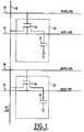
- FIG. 1illustrates a portion of an exemplary DRAM memory circuit containing two neighboring DRAM cells 42 .
- capacitor 44has two connections, located on opposite sides of the capacitor 44 .
- the first connectionis to a reference voltage, which is typically one half of the internal operating voltage (the voltage corresponding to one logical state) of the circuit.
- the second connectionis to the drain of the FET 46 .
- the gate of the FET 46is connected to the word line 48
- the source of the FETis connected to the bit line 50 .
- This connectionenables the word line 48 to control access to the capacitor 44 by allowing or preventing a signal (a logic “0” or a logic “1”) on the bit line 50 to be written to, or read from, the capacitor 44 .
- the body of the FET 46is connected to body line 76 , which is used to apply a fixed potential to the semiconductor body.
- the manufacturing of a DRAM celltypically includes the fabrication of a transistor, a capacitor, and three contacts: one each to the bit line, the word line, and the reference voltage Vr.
- DRAM manufacturingis a highly competitive business, there is continuous pressure to decrease the size of individual cells and to increase memory cell density to allow more memory to be squeezed onto a single memory chip, especially for densities greater than 256 Megabits.
- Limitations on cell size reductioninclude the passage of both active and passive word lines through the cell, the size of the cell capacitor, and the compatibility of array devices with non-array devices.
- a DRAM cellhaving an area of less than about 4F 2 that achieves high array density while maintaining structural commonality between array and peripheral (non-array) features. Also needed are simple methods of fabricating a DRAM cell that maximizes common process steps during the formation of array and peripheral devices.
- Exemplary embodiments of the present inventionprovide a DRAM cell array capable of achieving a cell area of less than about 4F 2 which comprises an array of vertical transistors with at least one buried bit line and at least one vertical gate electrode.
- the buried bit line and the vertical gate electrode of the vertical transistorsare substantially non-orthogonal.
- processes for fabricating DRAM cell arrays with vertical FET transistors having buried bit lines and vertical gate electrodesare also provided.
- FIG. 1is a schematic illustration of a known DRAM cell.
- FIG. 2is a cross-sectional view of a SOI substrate undergoing initial stages of a process according to a first embodiment of the present invention.
- FIG. 3shows the SOI substrate of FIG. 2 at a processing step subsequent to that shown in FIG. 2 .
- FIG. 4shows the SOI substrate of FIG. 2 at a processing step subsequent to that shown in FIG. 3 .
- FIG. 5shows the SOI substrate of FIG. 2 at a processing step subsequent to that shown in FIG. 4 .
- FIG. 6shows the SOI substrate of FIG. 2 at a processing step subsequent to that shown in FIG. 5 .
- FIG. 7shows two side-to-side cross-sectional views (A-A and B-B) of a SOI substrate of FIG. 11 undergoing the process according to the first embodiment of the present invention and at a processing step subsequent to that shown in FIG. 6 .
- FIG. 8shows the SOI substrate of FIG. 7 at a processing step subsequent to that shown in FIG. 7 .
- FIG. 9shows the SOI substrate of FIG. 7 at a processing step subsequent to that shown in FIG. 8 .
- FIG. 10shows the SOI substrate of FIG. 7 at a processing step subsequent to that shown in FIG. 9 .
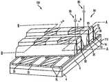
- FIG. 11is a perspective view of a memory array fabricated according to a first embodiment of the present invention.
- FIG. 12is a cross-sectional view of a wafer substrate undergoing the process according to a second embodiment of the present invention.
- FIG. 13shows the wafer of FIG. 12 at a processing step subsequent to that shown in FIG. 12 .
- FIG. 14shows the wafer of FIG. 12 at a processing step subsequent to that shown in FIG. 13 .
- FIG. 15shows the wafer of FIG. 12 at a processing step subsequent to that shown in FIG. 14 .
- FIG. 16shows the wafer of FIG. 12 at a processing step subsequent to that shown in FIG. 15 .
- FIG. 17shows two side-to-side cross-sectional views (A-A and B-B) of a semiconductor wafer of FIG. 18 undergoing the process according to the second embodiment of the present invention and at a processing step subsequent to that shown in FIG. 16 .
- FIG. 18is a perspective view of a memory array fabricated according to a second embodiment of the present invention.
- FIG. 19is a perspective view of a memory array fabricated according to a third embodiment of the present invention.
- FIG. 20is a cross-sectional view of a SOI substrate undergoing the process according to a fourth embodiment of the present invention.
- FIG. 21shows the SOI substrate of FIG. 20 at a processing step subsequent to that shown in FIG. 20 .
- FIG. 22shows the SOI substrate of FIG. 20 at a processing step subsequent to that shown in FIG. 21 .
- FIG. 23shows the SOI substrate of FIG. 20 at a processing step subsequent to that shown in FIG. 22 .
- FIG. 24shows the SOI substrate of FIG. 20 at a processing step subsequent to that shown in FIG. 23 .
- FIG. 25shows two side-to-side cross-sectional views (A-A and B-B) of a SOI substrate of FIG. 29 undergoing the process according to the fourth embodiment of the present invention and at a processing step subsequent to that shown in FIG. 24 .
- FIG. 26shows the cross-sectional views of the SOI substrate of FIG. 25 at a processing step subsequent to that shown in FIG. 25 .
- FIG. 27shows the cross-sectional views of the SOI substrate of FIG. 25 at a processing step subsequent to that shown in FIG. 26 .
- FIG. 28shows the cross-sectional views of the SOI substrate of FIG. 25 at a processing step subsequent to that shown in FIG. 27 .
- FIG. 29is a perspective view of a memory array fabricated according to a fourth embodiment of the present invention.
- FIG. 30is a cross-sectional view of a wafer substrate undergoing the process according to a fifth embodiment of the present invention.
- FIG. 31shows the wafer of FIG. 30 at a processing step subsequent to that shown in FIG. 30 .
- FIG. 32shows the wafer of FIG. 30 at a processing step subsequent to that shown in FIG. 31 .
- FIG. 33shows the wafer of FIG. 30 at a processing step subsequent to that shown in FIG. 32 .
- FIG. 34shows the wafer of FIG. 30 at a processing step subsequent to that shown in FIG. 33 .
- FIG. 35shows two side-to-side cross-sectional views (A-A and B-B) of a semiconductor wafer of FIG. 36 undergoing the process according to the second embodiment of the present invention and at a processing step subsequent to that shown in FIG. 35 .
- FIG. 36is a perspective view of a memory array fabricated according to a fifth embodiment of the present invention.
- FIG. 37is a perspective view of a memory array fabricated according to a sixth embodiment of the present invention.
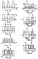
- FIG. 38is a top view of a mask array employed during the formation of the memory arrays fabricated according to the embodiments of the present invention.
- FIG. 39is a top view of a memory array including eight islands of the memory arrays fabricated according to the embodiments of the present invention.
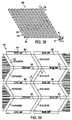
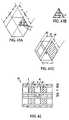
- FIGS. 40( a ) and ( b )are partial top views of a hexagonal layout of the memory array of FIG. 36 .
- FIG. 41( a )is a partial top view of one hexagonal unit cell.
- FIG. 41( b )is a partial top view of a single triangle of the hexagonal layout of the memory array of FIG. 41( a ).
- FIG. 41( c )is another top view of the hexagonal unit cell of FIG. 41( a ).
- FIG. 42is a partial top view of a square layout of a memory cell.
- FIG. 43illustrates a schematic diagram of a computer processor system which may utilize an imaging device, for example, a CMOS imaging device having a memory array fabricated according to methods of the present invention.
- an imaging devicefor example, a CMOS imaging device having a memory array fabricated according to methods of the present invention.
- substratein the following description may include any semiconductor-based structure on or at the surface of which circuitry may be formed.
- the structureshould be understood to include silicon, silicon-on insulator (SOI), silicon-on-sapphire (SOS), doped and undoped semiconductors, epitaxial layers of silicon supported by a base semiconductor foundation, and other semiconductor structures.
- SOIsilicon-on insulator
- SOSsilicon-on-sapphire
- doped and undoped semiconductorsepitaxial layers of silicon supported by a base semiconductor foundation, and other semiconductor structures.
- the semiconductorneed not be silicon-based.
- the semiconductorcould be silicon-germanium, germanium, or gallium arsenide.
- the exemplary embodiments described belowillustrate the formation of a DRAM cell having a cell size smaller than 4F 2 (where F is the minimum lithographic feature size), more preferably of about 3.464F 2 .
- the 3.464F 2 DRAM cell sizeis realizable through a novel “honeycomb” layout, which is a hexagonally-shaped layout that utilizes space efficiently, without sacrificing any lithography constraints.
- a novel “honeycomb” layoutwhich is a hexagonally-shaped layout that utilizes space efficiently, without sacrificing any lithography constraints.
- at least one buried bit line and at least one word line of the DRAM cellare placed at an angle other than a ninety degree angle, preferably at an angle ⁇ of about 60 degrees in relation to each other.
- the 4F 2 cell size of a square layoutbecomes a 3.464F 2 cell size corresponding to the hexagonal layout.
- the device array 100comprises a plurality of DRAM cells 99 formed over or within a substrate, for example over the illustrated SOI substrate 110 .
- Each DRAM cell 99comprises two devices, a vertical transistor 90 and a capacitor 80 located above the vertical transistor 90 having one electrode electrically connected to transistor 90 .
- each vertical transistor 90 of a particular column in the array 100is formed of drain 16 and source 12 , with double vertical gate electrode 35 formed over the thin gate oxide 34 of each transistor 90 .
- the gate electrodeis vertical and non-orthogonal to the buried bit line 25 .
- the vertical gate electrodeforms word line 35 which electrically connects all of the cells 99 of a given row in the array 100 .
- the vertical transistor 90comprises a vertical stack of three doped silicon layers 12 , 14 and 16 over an insulation layer 6 .
- An exemplary N-channel transistor 90as illustrated in FIG. 11 , would be formed using a SOI substrate 110 of a second conductivity type, for example n-type, a source 12 of the second conductivity type (n+), a lightly-doped body region 14 of a first conductivity type (p ⁇ ), and a drain 16 of the second conductivity type (n+). If P-channel devices were desired, the doping types and doping levels of these elements would be adjusted accordingly, as known in the art.
- the vertical transistor 90is a MOSFET (metal-oxide-semiconductor FET) device having doped region 12 coupled to a pair of buried bit lines (BL) 25 .
- the drain 16 of the transistor 90is in contact with one electrode of capacitor 80 .
- the buried bit lines 25preferably comprising a silicide material, are formed so that they contact the source 12 of each transistor 90 of a particular column in the array 100 .
- the device array 100is manufactured through a process described as follows and illustrated in FIGS. 2-10 .
- SOI substrate 110is formed by known methods in the art, for example, separation by implanted oxygen (SIMOX), bonding and etching back (BESOI), and zone melting and recrystallization (ZMR), among others.
- SIMOXseparation by implanted oxygen
- BESOIbonding and etching back
- ZMRzone melting and recrystallization
- the process for the formation of the SOI substrate 110starts with the preparation of a silicon substrate 4 ( FIG. 2 ).
- the silicon substrate 4is thermally oxidized to grow a layer of silicon oxide 6 ( FIG. 2 ) with a thickness of about 1 micron.
- a single crystalline silicon substrate 8is opposed to the silicon oxide layer 6 , as also shown in FIG. 2 .
- a resultant SOI substrate 110( FIG. 2 ) is formed of the silicon substrate 4 , the silicon oxide layer 6 , and the crystalline silicon substrate 8 .
- the first device layer 12is preferably a doped silicon layer of a second conductivity type (n+) approximately 0.4 microns thick, formed by implanting n-type dopants such as phosphorous (P), arsenic (As) or antimony (Sb) into crystalline silicon substrate 8 to form the n+ silicon layer 12 .
- a heat treatmentsuch as an anneal treatment at about 600° C.
- the second device layer 14is preferably a lightly-doped silicon layer of a first conductivity type (p ⁇ ); its thickness can be varied for desired channel lengths (e.g., about 0.05 to about 0.5 microns).
- the third device layer 16is also preferably a doped silicon layer of a second conductivity type (n+) about 0.2 microns thick. A heat treatment may be also optionally employed to activate the dopants within the p ⁇ silicon layer 14 and the n+ silicon layer 16 .
- an insulating layer 18is formed on top of the third device layer 16 by a deposition method or other suitable methods.
- the insulating layer 18may be also formed of silicon dielectrics such as silicon nitride or silicon oxide, but TEOS or carbides may be used also.
- insulating layer 18comprises a nitride material formed via CVD, PECVD and LPCVD deposition procedures, for example, at a temperature between about 300° C. to about 1000° C., to a thickness of about 500 Angstroms to about 2,000 Angstroms.
- a photoresist and mask 801( FIG. 38 ) are then applied over the insulating layer 18 , and photolithographic techniques are used to define a set of parallel rows on the array surface.
- a directional etching processsuch as plasma etching or reactive ion etching (RIE) is used to etch through the insulating layer 18 and through the device layers 16 , 14 and into device layer 12 to form a first set of trenches 21 , as depicted in FIG. 3 .
- the first set of trenches 21extends into the first device layer 12 about 1,000 Angstroms.
- a nitride film 22is formed on the sides of the first set of trenches 21 by depositing a layer of CVD nitride, for example, and directionally etching to remove excess nitride from horizontal surfaces.
- the nitride film 22( FIG. 3 ), which is about 100 Angstroms thick, acts as an oxidation and etching barrier during subsequent steps in the fabrication process.
- Anisotropic etchingsuch as RIE is subsequently conducted to deepen the first set of trenches 21 by about an additional 0.3 microns and to remove, therefore, the remainder of the n+ silicon layer 12 .
- a conductive layer 24 of a metal capable of forming a silicideis formed over gate stacks 20 , over the nitride spacers 22 and within the first set of trenches 21 by RF or DC sputtering, or by other similar methods such as CVD, to a thickness of about 100 Angstroms to about 800 Angstroms.
- the substrateis subjected to a rapid thermal anneal (RTA), typically for about 10 to 60 seconds, using a nitrogen ambient at about 600° C.
- RTArapid thermal anneal
- the metal capable of forming a silicideis a combination of cobalt/titanium nitride material that forms cobalt silicide bit line 25 .
- the metal silicidemay comprise any metal capable of forming a silicide, including but not limiting to cobalt, nickel, molybdenum, titanium, tungsten, tantalum, and platinum, among others, and combinations of such materials.
- the metal silicidemay also comprise combinations of silicides doped with nitrogen, such as cobalt nitride silicide, tungsten nitride silicide, or a combination of tungsten nitride silicide/tungsten silicide, for example.
- nitride material 26is formed within the first set of trenches 21 ( FIG. 6 ).
- the inventionalso contemplates the formation of an oxide, such as silicon oxide for example, to fill in the first set of trenches 21 .
- the device array 100is then planarized by any suitable means, such as chemical mechanical polishing (CMP), stopping at the third device layer 16 .
- CMPchemical mechanical polishing
- FIGS. 7-10schematically illustrate the formation of word lines 35 ( FIG. 10 ) of the vertical transistors 90 ( FIG. 11 ).
- FIGS. 7-10are illustrated as side-to-side cross-sectional views of the device array 100 of FIG. 11 , taken along lines A-A and B-B and at an initial stage of processing, but subsequent to the formation of the silicide bit lines 25 described above.
- the illustrations in FIGS. 7-10are cross-sectional views taken normal to the buried bit lines 25 (A-A), but at two different locations of the array 100 (A-A) and (B-B).
- FIG. 7illustrates stack 20 after the formation of the silicide bit lines 25 of FIG. 6 and after the formation of a second set of trenches 23 .
- the formation of the second set of trenches 23is similar to the formation of the first set of trenches 21 ( FIG. 3 ).
- a photoresist and mask 802FIG. 38 ) are applied over the third device layer 16 , and photolithographic techniques are used to define a set of parallel columns on the array surface.
- a directional etching processsuch as plasma etching or reactive ion etching (RIE) is used to etch through layer 26 , the device layers 16 , 14 and stopping on device layer 12 to form the second set of trenches 23 , as depicted in FIG. 7 .
- RIEreactive ion etching
- FIG. 8illustrates the next step in the process, in which the second set of trenches 23 ( FIG. 7 ) are filled with an insulating material 31 , preferably an oxide material such as silicon oxide, which is etched back by known methods in the art to form oxide layer 32 , as shown in FIG. 9 .
- the height of the oxide layer 32is tailored to allow isolation of the already-formed silicide bit lines 25 from the to-be-formed word lines or gate electrodes 35 .
- a thin gate oxide layer 34 and a gate electrode 35are sequentially formed on the sidewalls of the stacks 20 , as shown in FIG. 10 .
- the thin gate oxide layer 34which will act as a gate insulator layer, may comprise silicon dioxide (SiO 2 ), for example, which may be thermally grown in an oxygen ambient, at a temperature between about 600° C. to about 1000° C. and to a thickness of about 10 Angstroms to about 100 Angstroms.
- the gate insulatoris not limited to silicon oxide and other dielectric materials such as oxynitride, Al 2 O 3 , Ta 2 O 5 or other high k material may be used as gate insulator layer.
- a gate layer 35is formed over the thin gate oxide layer 34 .
- the gate layer 35is formed of doped polysilicon, for example, which may be deposited over the thin gate oxide layer 34 by, for example, a low plasma chemical vapor deposition (LPCVD) method at a temperature of about 300° C. to about 700° C. and to a thickness of about 100 Angstroms to about 2,000 Angstroms.
- LPCVDlow plasma chemical vapor deposition
- Anisotropic plasma etchingis conducted to define the gate electrode 35 non-orthogonal to the buried silicide bit lines 25 .
- the gate electrode 35is formed at an angle ⁇ ( FIG. 11 ), preferably of about 60 degrees, with the bit lines 25 .
- Each of the vertical transistor 90 of a particular column in the array 100is formed of drain 16 and source 12 , with double vertical gate electrode 35 formed over the thin gate oxide 34 of each transistor 90 .
- the gate electrodeis vertical and non-orthogonal to the buried bit line 25 .
- the double vertical gate electrode 35forms an angle ⁇ of about 60 degrees with the buried bit line 25 .
- the vertical gate electrodeforms word line 35 which electrically connects all of the cells 99 of a given row in the array 100 .
- Conventional processing methodsmay then be used to form contacts and wirings to connect the device array to peripheral circuits, and to form other connections.
- the entire surfacemay be covered with a passivation layer of, for example, silicon dioxide, BSG, PSG, or BPSG, which is CMP planarized and etched to provide capacitor trenches over the transistors 90 , in which capacitors 80 are formed, as well as contact holes which may then be metallized to interconnect the word lines, bit lines and capacitors 80 of the memory cells 99 into an operative memory array.
- Conventional multiple layers of conductors and insulatorsmay also be used to interconnect the structures.
- the device array 200comprises a plurality of DRAM cells 299 formed over or within a p-type wafer substrate 210 , and not within a SOI substrate, such as the SOI substrate 110 of the previously-described embodiment.
- each DRAM cell 299comprises two devices, a vertical transistor 290 and a capacitor 80 located above the transistor 290 .
- the gate layer 35is vertical and non-orthogonal to the buried bit line 25 formed within the p-type substrate 210 .
- the transistor 290is formed of a vertical stack of three doped silicon layers formed by appropriately doping the p-type wafer substrate 210 .
- An exemplary n-channel device, as illustrated in FIG. 18would be formed using a wafer substrate 210 of a first conductivity type, for example p+, a source 12 of a second conductivity type (n+), a lightly-doped body region 14 of a first conductivity type (p ⁇ ), and a drain 16 of a second conductivity type (n+). If p-channel devices were desired, the doping types and levels of these elements would be adjusted accordingly, as known in the art.
- the drain 16 of the transistor 290is in contact with one electrode of capacitor 80 .
- Buried silicide bit line 25is formed of a conductive silicide and contacts the source 12 of each transistor 290 of a particular column in the array 200 .
- Active word line or gate electrode 35is formed of a conductive material such as doped polysilicon of a second conductivity type (n+) and acts as the gate of each transistor 290 to electrically connect all of the cells 299 of a given row in the array 200 .
- FIGS. 12-17illustrate the processing steps for the formation of the device array 200 manufactured in accordance with a second embodiment of the present invention. As noted above, these processing steps are similar in part with the processing steps of FIGS. 2-10 but differ in that the SOI substrate 110 of the first embodiment is replaced with a p-type substrate 210 in the second embodiment. Accordingly, for exemplary purposes only, the substrate 210 will be described as a silicon substrate, and the following process should be modified as appropriate and as known in the art if a non-silicon substrate is used.
- the substrate 210may be doped or undoped, but a p-type doped substrate is preferred.
- substrate 210may be a doped silicon substrate having an active dopant concentration within the range of about 1 ⁇ 10 16 to 1 ⁇ 10 18 atoms per cm 3 , more preferably about 5 ⁇ 10 16 to 5 ⁇ 10 17 atoms per cm 3 .
- Device layers 12 , 14 , 16are next formed by doping or implanting areas of the p-type substrate 210 appropriately with p-type or n-type dopants to form n+, p ⁇ , n+ regions or layers 12 , 14 , 16 .
- the first device layer 12is preferably formed as a doped silicon layer of a second conductivity type (n+) and about 0.4 microns thick, by implanting n-type dopants such as phosphorous (P), arsenic (As) or antimony (Sb) into p-type substrate 210 to form the n+ silicon layer 12 .
- n-type dopantssuch as phosphorous (P), arsenic (As) or antimony (Sb)
- the second device layer 14is preferably formed as a lightly-doped silicon layer of a first conductivity type (p ⁇ ) and has a thickness that can be varied for desired channel length (e.g., about 0.05 to about 0.5 microns).
- the third device layer 16is preferably formed as a doped silicon layer of a second conductivity type (n+) about 0.2 microns thick.
- a heat treatmentsuch as an anneal treatment at about 600° C. to about 1000° C., may be optionally used to activate the dopants within the n+ silicon layer 12 , the p ⁇ silicon layer 14 and the n+ silicon layer 16 .
- the remaining portion of the substrate 210is illustrated in FIG. 12 as substrate 210 a.
- an insulating layer 18is formed on top of the third device layer 16 by chemical vapor deposition (CVD) or other suitable methods.
- a photoresist and mask 801( FIG. 38 ) are then applied over the first insulating layer 18 , and photolithographic techniques are used to define a set of parallel rows on the array surface.
- a directional etching processsuch as plasma etching or reactive ion etching (RIE) is used to etch through the insulating layer 18 and through the device layers 14 , 16 and into device layer 12 of the substrate 210 to form a first set of trenches 21 , as depicted in FIG. 12 .
- the first set of trenches 21extends into the first device layer 12 about 1,000 Angstroms.
- a nitride film 22( FIG. 12 ) is formed on the sides of the first set of trenches 21 by depositing a layer of CVD nitride, for example, and directionally etching to remove excess nitride from horizontal surfaces.
- the nitride film 22which is about 100 Angstroms thick, acts as an oxidation and etching barrier during subsequent steps in the fabrication process.
- Anisotropic etchingsuch as RIE is subsequently conducted to deepen the first set of trenches 21 by about an additional 0.3 microns and to remove, therefore, the remainder of the n+ silicon layer 12 .
- a conductive layer 24 ( FIG. 13 ) of a metal capable of forming a silicideis next formed over gate stacks 120 , over the nitride spacers 22 and within the first set of trenches 21 ( FIG. 13 ).
- the conductive layer 24may be formed by RF or DC sputtering, or by other similar methods such as CVD, to a thickness of about 100 Angstroms to about 800 Angstroms.
- the substrateis subjected to a rapid thermal anneal (RTA), typically for about 10 to 60 seconds, using a nitrogen ambient at about 600° C.
- RTArapid thermal anneal
- a distance “d”( FIG. 16 ) of about 700 Angstroms must be maintained between lower surface 25 b of the buried bit lines 25 and upper surface 210 b of the p-type substrate 210 .
- the metal capable of forming a silicidemay preferably be a combination of cobalt/titanium nitride material that forms cobalt silicide bit line 25 .
- the metal silicidemay comprise any metal capable of forming a silicide, including but not limiting to cobalt, nickel, molybdenum, titanium, tungsten, tantalum, and platinum, among others, and combinations of such materials.
- the metal silicidemay also comprise combinations of silicides doped with nitrogen, such as cobalt nitride silicide, tungsten nitride silicide, or a combination of tungsten nitride silicide/tungsten silicide, for example.
- nitride material 26is preferred, the invention also contemplates the formation of an oxide, such as silicon oxide for example, to fill in the first set of trenches 21 .
- the device array 200is then planarized by chemical mechanical polishing (CMP), for example, stopping at the third device layer 16 .
- CMPchemical mechanical polishing
- a second set of trenches( FIG. 17 ) are formed by directional etching, for example, as explained above for trenches 23 with reference to FIGS. 7-10 .
- the second set of trenchesare formed by employing again mask 802 ( FIG. 38 ).
- the second set of trenchesare then filled with an insulating material, preferably an oxide material such as silicon oxide, which is etched back by known methods in the art to form an oxide layer (not shown) similar to oxide layer 32 of FIG. 9 .
- a thin gate oxide layer 34 and a gate electrode 35are sequentially formed on the sidewalls of the stacks 20 , as shown in FIG. 17 .
- the thin gate oxide layer 34 and word lines or gate electrodes 35 ( FIG. 17 ) of the vertical transistors 290 ( FIG. 18 )are formed as described above with reference to the formation of the word lines or gate electrodes of the first embodiment of the present invention.
- the thin gate oxide layer 34which will act as a gate insulator layer, may comprise silicon dioxide (SiO 2 ), for example, which may be thermally grown in an oxygen ambient, at a temperature between about 600° C. to about 1000° C.
- Gate layer 35may be formed of polysilicon which may be deposited over the thin gate oxide layer 34 by, for example, a low plasma chemical vapor deposition (LPCVD) method at a temperature of about 300° C. to about 700° C. and to a thickness of about 100 Angstroms to about 2,000 Angstroms.
- LPCVDlow plasma chemical vapor deposition
- Each of the vertical transistor 290 of a particular row in the array 200is formed of drain 16 and source 12 , with gate layer 35 formed over the thin gate oxide 34 of each vertical transistor 290 .
- the gate layer 35is vertical and non-orthogonal to the buried bit line 25 formed within the p-type substrate 210 a .
- the gate layer 35may form an angle ⁇ ( FIG. 18 ) of about 60 degrees with the buried bit line 25 .
- the vertical gate layerforms word line 35 which electrically connects all of the cells 299 of a given row in the array 200 .
- Capacitorsare formed over the vertical transistors 290 with one electrode in contact with drain 16 .
- Other processing stepsare then carried out to interconnect the word line, bit lines and capacitors of the memory cells 299 in a memory array, as described above with reference to the first embodiment.
- FIG. 19illustrates yet another embodiment of the present invention according to which the device array 300 comprises MOSFET transistors 390 which are subjected to an optional salicide process after the formation of double vertical gate electrode 335 .
- the MOSFET transistors 390may be formed over or within a SOI substrate (as the SOI substrate 110 described above in the first embodiment and with reference to FIGS. 2-11 ) or over or within a wafer substrate (as the p-type substrate 210 described above in the second embodiment and with reference to FIGS. 12-18 ).
- the MOSFET transistors 390are fabricated as described above within a p-type substrate 210 , in a manner similar to that for the formation of the MOSFET transistors 290 of FIG. 18 .
- the arrayis subjected to another metal deposition and anneal process such as a rapid thermal anneal (RTA) for about 10 to 60 seconds using a nitrogen ambient at about 600° C. to about 850° C., to form word lines or gate electrodes 335 ( FIG. 19 ) of metal silicides and a layer 385 that forms over all exposed silicon (including gate electrodes 335 and silicon adjacent to buried bit lines 25 ) ( FIG.
- RTArapid thermal anneal
- the word line 335 , the buried bit line 25 and the drain including layer 385are all formed of a silicide material.
- the word line 335forms an angle other than a ninety degree angle (for example, an angle ⁇ ( FIG. 19 ) of about 60 degrees) with the buried bit line 25 .
- FIGS. 20-29illustrate a fourth embodiment of the present invention, according to which device array 400 ( FIG. 29 ) comprises a plurality of DRAM cells 499 , each DRAM cell 499 comprising two devices, a vertical transistor 490 and a capacitor 80 located above the transistor 490 .
- Vertical transistor 490 of the device array 400comprises buried bit lines 25 disposed adjacent a gate stack comprising epitaxial layers 414 , 416 , 418 , and not doped silicon layers as in the previously-described embodiments.
- FIG. 20illustrates a SOI substrate 110 similar to that shown in FIG. 2 .
- the SOI substrate 110may be formed by a bonding and etching back method, according to which a silicon substrate 4 is thermally oxidized to grow a layer of silicon oxide 6 with a thickness of about 1 micron.
- a silicon substrate 4is thermally oxidized to grow a layer of silicon oxide 6 with a thickness of about 1 micron.
- an n-type single crystalline silicon substrate 8is opposed to the silicon oxide layer 6 , and the silicon substrate 4 , with the oxide layer 6 , is then contacted with the crystalline silicon substrate 8 , and the resultant structure is heated to a temperature of about 1000° C., so that the n-type crystalline silicon of the crystalline silicon substrate 8 adheres to the silicon oxide layer 6 .
- the n-type crystalline silicon substrate 8may be polished so that its thickness may be decreased.
- the resultant SOI substrate 110is formed of the silicon substrate 4 , the silicon oxide layer 6 , and the
- a thick insulating layer 51for example a thick oxide layer or a thick nitride layer of about 2,000 Angstroms to about 10,000 Angstroms, is formed over the SOI substrate 110 by chemical vapor deposition (CVD) or other suitable methods, for example.
- the insulating layer 51may be formed via PECVD and LPCVD deposition procedures, for example, at a temperature between about 300° C. to about 1000° C.
- a photoresist and mask 801( FIG. 38 ) are then applied over the thick insulating layer 51 , and photolithographic techniques and mask 801 ( FIG. 38 ) are used to define a set of parallel rows or columns 51 a on the array surface.
- a directional etching processsuch as plasma etching or reactive ion etching (RIE) is used to etch through the insulating layer 51 and into the SOI substrate 110 to form a first set of trenches 21 , as depicted in FIG. 20 .
- the first set of trenchesextend into the crystalline silicon substrate 8 and stop on the upper surface of the silicon oxide layer 6 , as shown in FIG. 20 .
- a conductive layer 24 of a metal capable of forming a silicideis formed over insulating columns 51 a and within the first set of trenches 21 ( FIG. 21 ) by RF or DC sputtering, or by other similar methods such as CVD, to a thickness of about 100 Angstroms to about 800 Angstroms.
- the substrateis subjected to a rapid thermal anneal (RTA), typically for about 10 to 60 seconds, using a nitrogen ambient at about 600° C. to about 850° C., so that the metal in direct contact with the silicon layer 8 is converted to its silicide and forms buried silicide regions 25 ( FIG.
- RTArapid thermal anneal
- the metal capable of forming a silicideis a combination of cobalt/titanium nitride material that forms cobalt silicide bit line 25 .
- the metal silicidemay comprise any metal capable of forming a silicide, including but not limiting to cobalt, nickel, molybdenum, titanium, tungsten, tantalum, and platinum, among others, and combinations of such materials.
- the metal silicidemay also comprise combinations of silicides doped with nitrogen, such as cobalt nitride silicide, tungsten nitride silicide, or a combination of tungsten nitride silicide/tungsten silicide, for example.
- nitride material 26is formed within the first set of trenches 21 , as shown in FIG. 22 .
- nitride materialis preferred, the invention also contemplates the formation of an oxide, such as silicon oxide for example, to fill in the first set of trenches 21 , but must be dissimilar to the material of insulating layer 51 .
- the device array 400is then planarized by any suitable means, such as chemical mechanical polishing (CMP), stopping at the insulating columns 51 a , and the insulating columns 51 a are subsequently removed by known methods in the art to form the structure of FIG. 23 .
- CMPchemical mechanical polishing
- FIG. 24illustrates epitaxial silicon layers 414 , 416 , 418 formed within trenches 21 a ( FIG. 23 ) by known methods, for example, by epitaxial growth, such as vapor phase, liquid phase, or solid phase epitaxy.
- the first epitaxial silicon layer 414may be grown by epitaxy in a reaction chamber at high temperatures, of about 900-1200° C., and by employing a silicon gas source that introduces a gaseous species containing silicon (Si) into the reaction chamber.
- the silicon gas sourcemay be silane (SiH 4 ), higher order silanes, such as disilane (Si 2 H 6 ), as well as other gaseous sources of silicon, such as dichlorsilane (SiH 2 Cl 2 ), trichlorsilane (SiHCl 3 ), or tetrachlorsilane (SiCl 4 ), for example.
- the first epitaxial silicon layer 414is grown over the SOI substrate 110 to a thickness of about 500 to about 3,000 Angstroms, preferably of about 2,000 Angstroms.
- n-type dopantssuch as phosphorous (P), arsenic (As) or antimony (Sb) are introduced into the first epitaxial silicon layer 414 to form an n-type epitaxial silicon layer 414 .
- a heat treatmentsuch as an anneal treatment at about 600° C. to about 1000° C., may be optionally employed to activate the dopant within the n+ epitaxial silicon layer 414 .
- a second epitaxial silicon layer 416 and a third epitaxial silicon layer 418are sequentially formed over the first epitaxial silicon layer 414 , as shown in FIG. 24 , by methods similar to, or different from, those employed for the formation of the first epitaxial silicon layer 414 .
- the second epitaxial silicon layer 416is doped with a p-type dopant, such as boron (B), boron fluoride (BF 2 ) or indium (In), and is formed to a thickness of about 500 to about 2,000 Angstroms.
- the third epitaxial silicon layer 418is doped with an n-type dopant, different from or similar to that for the formation of the n-type first epitaxial silicon layer 414 , and is formed to a thickness of about 500 to about 1,500 Angstroms, preferably of about 1,000 Angstroms.
- a heat treatmentfor example, an anneal treatment at about 600° C. to about 1000° C., may be optionally employed to activate the dopant within each of the second and third epitaxial silicon layers 416 , 418 .
- FIGS. 25-28correspond to FIGS. 7-10 of the first embodiment, and illustrate side-to-side cross-sectional views of the device array 400 of FIG. 29 , taken along lines A-A and B-B and at an initial stage of processing, but subsequent to the formation of the silicide bit lines 25 described above.
- the illustrations in FIGS. 25-28are cross-sectional views taken normal to the buried bit lines 25 but at two different locations at the array 400 (A-A) and (B-B).
- FIG. 25illustrates gate stack 420 comprising epitaxial silicon layers 414 , 416 , 418 after the formation of the silicide bit lines 25 of FIG. 24 .
- FIG. 26illustrates the next step in the process, in which second set of trenches 23 ( FIG. 25 ) are formed with the mask 802 of FIG. 38 and then filled with an insulating material 31 , preferably an oxide material such as silicon oxide, which is etched back by known methods in the art to form oxide layer 32 , as shown in FIG. 27 .
- the height of the oxide layer 32is tailored to allow isolation of the already-formed silicide bit lines 25 from the to-be-formed word lines 435 .
- the thin gate oxide layer 434which will act as a gate insulator layer, may comprise silicon dioxide (SiO 2 ), for example, which may be thermally grown in an oxygen ambient, at a temperature between about 600° C. to about 1000° C. and to a thickness of about 10 Angstroms to about 100 Angstroms.
- the gate insulatoris not limited to silicon oxide and other dielectric materials such as oxynitride, Al 2 O 3 , Ta 2 O 5 or other high k material may be used as gate insulator layer.
- gate layer 435is formed over the thin gate oxide layer 434 .
- the gate layer 435is formed of doped polysilicon which may be formed over the thin gate oxide layer 434 by, for example, a low plasma chemical vapor deposition (LPCVD) method at a temperature of about 300° C. to about 700° C. and to a thickness of about 100 Angstroms to about 2,000 Angstroms.
- LPCVDlow plasma chemical vapor deposition
- An anisotropic RIEis then used to define the double gate electrode 435 non-orthogonal to the buried silicide bit lines 25 .
- Subsequent processing stepsare then applied to complete the formation of the device array 400 comprising MOSFET transistor 490 .
- Each of the vertical transistor 490 of a particular column in the array 400is formed of drain 418 and source 414 , with double gate electrode 435 formed over the thin gate oxide 34 of each transistor 490 .
- the gate electrodeis vertical and forms an angle other than a ninety degree angle (for example, an angle ⁇ ( FIG. 29 ) of about 60 degrees) with the buried bit line 25 .
- the vertical gate electrodeforms word line 435 which electrically connects all of the cells 499 of a given row in the array 400 .
- capacitorsare formed over the vertical transistors 490 with one electrode in contact with drain 418 .
- Other processing stepsare then carried out to interconnect the word line, bit lines and capacitors of the memory cells 499 in a memory array, as described above with reference to the first embodiment.
- FIGS. 30-36illustrate a fifth embodiment of the present invention, according to which epitaxial silicon layers 414 , 416 , 418 are formed as part of stack 420 provided over a p-type silicon wafer 210 , and not over a SOI substrate, such as the SOI substrate 110 described above.
- epitaxial silicon layers 414 , 416 , 418are formed as part of stack 420 subsequent to the formation of the silicide bit lines 25 of FIG. 33 , and as part of DRAM cells 599 of device array 500 ( FIG. 36 ).
- FIG. 30illustrates the formation of an n+ silicon layer 12 and a thick insulating layer 51 of about 2,000 Angstroms to about 10,000 Angstroms, which are formed over the p-type silicon wafer 210 by chemical vapor deposition (CVD) or other suitable methods, for example.
- the n+ silicon layer 12may be also formed by appropriately doping a top portion of the p-type silicon wafer 210 , as explained above with reference to the previously described embodiments.
- the insulating layer 51may be formed via PECVD and LPCVD deposition procedures, for example, at a temperature between about 300° C. to about 1000° C.
- a photoresist and mask 801( FIG. 38 ) are then applied over the thick insulating layer 51 , and photolithographic techniques are used to define a set of parallel oxide rows 51 a on the array surface.
- a directional etching processsuch as plasma etching or reactive ion etching (RIE) is used to etch into the n+ silicon layer 12 to form a first set of trenches 21 , as depicted in FIG. 30 .
- a conductive layer 24 of a metal capable of forming a silicideis formed over insulating columns 51 a and within the first set of trenches 21 ( FIG. 31 ) by RF or DC sputtering, or by other similar methods such as CVD, to a thickness of about 100 Angstroms to about 800 Angstroms.
- the substrateis subjected to a rapid thermal anneal (RTA), typically for about 10 to 60 seconds, using a nitrogen ambient at about 600° C.
- RTArapid thermal anneal
- the metal capable of forming a silicidemay be the same as, or different from, the metals capable of forming silicides described above with reference to the formation of the buried silicide regions 25 of the previous embodiments. It must be noted, however, that no silicide forms within the p-type substrate 210 . Preferably, a distance “d” ( FIG. 34 ) of about 700 Angstroms must be maintained between lower surface 25 b of the buried bit lines 25 and upper surface 210 b of the p-type substrate 210 .
- the unreacted metalis stripped ( FIG. 33 ) and the silicide is etched together with the n+ silicon layer 12 down to the p-type silicon substrate 210 and a nitride material 26 is formed within the first set of trenches 21 , as shown in FIG. 34 .
- nitride materialis preferred, the invention also contemplates the formation of an oxide, such as silicon oxide for example, to fill in the first set of trenches 21 , but it must be dissimilar to the material of the insulating layer 51 .
- the device array 500is then planarized by any suitable means, such as chemical mechanical polishing (CMP), for example, stopping at the insulating columns 51 a.
- CMPchemical mechanical polishing
- epitaxial silicon layers 414 , 416 , 418are formed by known methods, for example, by epitaxial growth, such as vapor phase, liquid phase, or solid phase epitaxy.
- the first epitaxial silicon layer 414may be grown by epitaxy in a reaction chamber at high temperatures, of about 900-1200° C., and by employing a silicon gas source that introduces a gaseous species containing silicon (Si) into the reaction chamber.
- the silicon gas sourcemay be silane (SiH 4 ), higher order silanes, such as disilane (Si 2 H 6 ), as well as other gaseous sources of silicon, such as dichlorsilane (SiH 2 Cl 2 ), trichlorsilane (SiHCl 3 ), or tetrachlorsilane (SiCl 4 ), for example.
- the first epitaxial silicon layer 414is grown over the substrate 210 to a thickness of about 500 to about 3,000 Angstroms, preferably of about 2,000 Angstroms.
- n-type dopantssuch as phosphorous (P), arsenic (As) or antimony (Sb) are introduced into the first epitaxial silicon layer 414 to form an n-type epitaxial silicon layer 414 .
- a heat treatmentsuch as an anneal treatment at about 600° C. to about 1000° C., may be optionally employed to activate the dopant within the n+epitaxial silicon layer 414 .
- a second epitaxial silicon layer 416 and a third epitaxial silicon layer 418are sequentially formed over the first epitaxial silicon layer 414 , as shown in FIG. 35 , by methods similar to, or different from, those employed for the formation of the first epitaxial silicon layer 414 .
- the second epitaxial silicon layer 416is doped with a p-type dopant, such as boron (B), boron fluoride (BF 2 ) or indium (In), and is formed to a thickness of about 500 to about 2,000 Angstroms.
- the third epitaxial silicon layer 418is doped with an n-type dopant, different from or similar to that for the formation of the n-type first epitaxial silicon layer 414 , and is formed to a thickness of about 500 to about 1,500 Angstroms, preferably of about 1,000 Angstroms.
- a heat treatmentfor example, an anneal treatment at about 600° C. to about 1000° C., may be optionally employed to activate the dopant within each of the second and third epitaxial silicon layers 416 , 418 .
- gate electrode lines 535 or word lines 535 ( FIG. 35 ) of the vertical transistors 590proceeds according to a method similar to that described above with reference to the first embodiment and as shown in FIGS. 7-10 .
- a thin gate oxide layer 534 and a gate electrode 535are sequentially formed on the sidewalls of the stacks 420 , as shown in FIG. 35 .
- the thin gate oxide layer 534which will act as a gate insulator layer, may comprise silicon dioxide (SiO 2 ), for example, which may be thermally grown in an oxygen ambient, at a temperature between about 600° C. to about 1000° C.
- the gate insulatoris not limited to silicon oxide and other dielectric materials such as oxynitride, Al 2 O 3 , Ta 2 O 5 or other high k material may be used as gate insulator layer.
- Vertical double gate electrode 535is formed over the thin gate oxide layer 534 and is non-orthogonal to the buried silicide bit lines 25 . Subsequent processing steps are then applied to complete the formation of the device array 500 comprising MOSFET transistors 590 ( FIG. 36 ). Each of the vertical transistor 590 of a particular column in the array 500 is formed of drain 418 and source 414 , with double gate electrode 535 formed over the thin gate oxide 534 of each transistor 590 . The gate electrode is vertical and non-orthogonal to the buried bit line 25 . The vertical gate electrode forms word line 535 which electrically connects all of the cells 599 of a given row in the array 500 . Subsequent processing steps are then carried out to interconnect the word lines, the bit lines and capacitors of the memory cells 599 in a memory array, as described above with reference to the first embodiment.
- FIG. 37illustrates yet another embodiment of the present invention according to which the device array 600 comprises MOSFET transistors 690 which are subjected to an optional salicide process after the formation of the vertical gate electrode 435 , 535 ( FIGS. 29 and 36 ).
- the MOSFET transistors 690may be formed over a SOI substrate (as the SOI substrate 110 described above with reference to FIGS. 20-29 ) or over a p-type substrate (as the p+ substrate 210 described above with reference to FIGS. 30-36 ) and comprises epitaxial silicon layers 414 , 416 , 418 formed as part of stack 420 and as described in detail above.
- the MOSFET transistors 690are fabricated as described above over a p-type substrate 210 , in a manner similar to that for the formation of the MOSFET transistors 590 of FIG. 36 .
- the array 600is subjected to another metal deposition and anneal process such as a rapid thermal anneal (RTA) for about 10 to 60 seconds using a nitrogen ambient at about 600° C.
- RTArapid thermal anneal
- gate electrodes 535 of metal silicides and a silicide layer 685that forms over all exposed silicon (including gate electrodes 535 and silicon adjacent to buried bit lines 25 )) preferably of cobalt silicide (CoSi 2 ), or other silicide material.
- the cobalt silicide formed on top of the stack 420may be formed simultaneously with the formation of the buried silicide bit lines 25 or, alternatively, after the formation of the buried silicide bit lines 25 (i.e., after gate electrode formation).
- the metal for the formation of the silicide gate electrode 535must be a metal which may be converted to its silicide or a combination of such metals, for example.
- the word line 535(which is non-orthogonal to the buried line 25 ), the buried bit line 25 and the drain including layer 685 are all formed of a silicide material.
- FIG. 38illustrates a die setup 800 comprising at least two masks 801 , 802 which are employed for the formation of the device arrays described above, wherein at least one buried bit line and at least one double vertical gate electrode of the arrays described above are formed at an angle “ ⁇ ” which is different than a ninety degree angle.
- FIG. 39illustrates a schematic top view of eight memory arrays described above and formed according to embodiments of the present invention incorporated with sense amplifiers 710 and row drivers 720 .
- FIG. 39illustrate device array 700 including eight memory arrays 600 , described above with reference to FIG. 37 , and incorporated with sense amplifiers 710 and row drivers 720 .
- FIGS. 40( a ) and ( b )illustrate partial top views of the device array 600 of FIG. 37 showing the formation of the buried bit lines 25 and of the double vertical gate electrode 535 at an angle ⁇ of about 60 degrees and as part of a “honeycomb” or hexagonally shaped layout 888 .
- FIGS. 41 and 42illustrate a side-by-side comparison of a hexagonal unit A ( FIG. 41( a )) of the hexagonally shaped layout 888 (or “honeycomb” layout) of FIG. 40 and of a square unit B of a squarely shaped layout.
- the area of a single triangle A 1 of the hexagonal unit of FIG. 41( a )is of about 0.5774 F 2 , where F is the minimum lithographic feature size.
- the area of the hexagon unit A of FIGS. 41( a ) and 41 ( c )is (6 ⁇ 0.5774 F 2 ) or about 3.464 F 2 .
- the area of the single square B 1 of the squarely shaped layout of FIG. 42is about 4 F 2 .
- the difference in the sizes of the hexagonal unit A and of the square unit Bdemonstrates that, by employing the buried bit line and the word line of the DRAM cells of the previously-described embodiments at an angle other than a ninety degree angle, the 4F 2 cell size of a square layout becomes a 3.464F 2 DRAM cell size corresponding to the hexagonal layout. This, in turn, reduces the cell size by about 13.4% (and the array area savings by about 13.4%).
- employing a hexagonal layout in lieu of a square layoutallows a larger landing pad (of about 15.5% larger) for a capacitor of a hexagonal layout. This is because the landing pad for a square layout is of about 1F 2 while the landing pad for a hexagonal layout is 1.155 F 2 .
- the width of a FET formed by employing the honeycomb layout of the present inventionis about 15.47% larger for each gate (and about 31% for double gate electrode).
- the bit line to bit line cross talk in the device array 700( FIG. 39 ) is also reduced, as the average separation between two adjacent buried bit lines of the hexagonal array 700 is of about 0.539F, compared to the 0.5F average separation between two adjacent buried bit lines of a square array.
- the word line to word line cross talk in the device array 700is also reduced, as the average separation between two adjacent word lines of the hexagonal array 700 is of about 1.077F, compared to the 1F average separation between two adjacent word lines of a square array.
- NMOS vertical transistorshaving at least a double buried bit line forming an angle other than a 90 degree angle with at least a double vertical gate electrode
- the inventionis not limited to this embodiment. Accordingly, the invention also contemplates the formation of PMOS transistors, as well as the formation of a plurality of MOS transistors of the same or different conductivity type.
- the above illustrated and described embodimentsare only exemplary, and the present invention is not limited to the illustrated embodiments.
- FIG. 43illustrates system 700 , a typical processor system modified to include an imaging device 708 comprising at least a DRAM cell having an area less than 4F 2 , more preferably of about 3.464F 2 and constructed in accordance with an embodiment of the invention (e.g., DRAM cell 99 of FIG. 11 ).
- the processor-based system 700is exemplary of a system having digital circuits that could include image sensor devices. Without being limiting, such a system could include a computer system, camera system, scanner, machine vision, vehicle navigation, video phone, surveillance system, auto focus system, star tracker system, motion detection system, image stabilization system, and data compression system.
- System 700for example a camera system, generally comprises a central processing unit (CPU) 702 , such as a microprocessor, that communicates with an input/output (I/O) device 706 over a bus 704 .
- Imaging device 708also communicates with the CPU 702 over the bus 704 .
- the processor-based system 700also includes random access memory (RAM) 710 , and can include removable memory 715 , such as flash memory, which also communicate with the CPU 702 over the bus 704 .
- the imaging device 708may be combined with a processor, such as a CPU, digital signal processor, or microprocessor, with or without memory storage on a single integrated circuit or on a different chip than the processor.
- n+, p ⁇ , n+ regions or device layers 12 , 14 , 16has been described above with reference to the doping of a SOI substrate (such as SOI substrate 110 ) or of a silicon substrate (such as p-type silicon substrate 210 ), the invention is not limited to these embodiments and also contemplates the formation of device layers 12 , 14 , 16 by other known methods in the art.
- device layers 12 , 14 , 16may be doped silicon or doped polysilicon layers formed over a SOI substrate or over a silicon substrate, or partially within a SOI substrate or a silicon substrate.
- the n+, p ⁇ , n+ regions or device layers 12 , 14 , 16may be formed by deposition methods, for example, by CVD, PECVD or LPCVD, among others, or by other known methods of the art. Accordingly, the embodiments described above with reference to the formation of n+, p ⁇ , n+ regions or device layers 12 , 14 , 16 by doping or implanting predefined regions of a SOI substrate or of a p-type silicon substrate are only exemplary, and the invention is not limited to these exemplary embodiments.
- the above embodimentshave been described with reference to the formation of vertical transistors having at least a double buried bit line and at least a double vertical gate electrode that are non-orthogonal relative to each other, it must be understood that the invention is not limited to these embodiments. Accordingly, the invention also contemplates the formation of vertical transistors having only one buried bit line formed by the embodiments described above. The invention also contemplates embodiments in which the buried bit line of the vertical transistor is at least partially buried and not completely buried, as described in the embodiments above. Further, the invention does not contemplate embodiments where only pairs of bit lines or pairs of gates are formed associated with each vertical transistor. Thus, the invention could be adapted for use to form one bit line and one vertical gate per transistor.
Landscapes
- Engineering & Computer Science (AREA)
- Manufacturing & Machinery (AREA)
- Semiconductor Memories (AREA)
Abstract
Description
Claims (69)
Priority Applications (4)
| Application Number | Priority Date | Filing Date | Title |
|---|---|---|---|
| US10/928,315US7365385B2 (en) | 2004-08-30 | 2004-08-30 | DRAM layout with vertical FETs and method of formation |
| US11/328,150US7560336B2 (en) | 2004-08-30 | 2006-01-10 | DRAM layout with vertical FETs and method of formation |
| US12/076,766US7968928B2 (en) | 2004-08-30 | 2008-03-21 | DRAM layout with vertical FETs and method of formation |
| US13/109,753US8389360B2 (en) | 2004-08-30 | 2011-05-17 | DRAM layout with vertical FETs and method of formation |
Applications Claiming Priority (1)
| Application Number | Priority Date | Filing Date | Title |
|---|---|---|---|
| US10/928,315US7365385B2 (en) | 2004-08-30 | 2004-08-30 | DRAM layout with vertical FETs and method of formation |
Related Child Applications (2)
| Application Number | Title | Priority Date | Filing Date |
|---|---|---|---|
| US11/328,150DivisionUS7560336B2 (en) | 2004-08-30 | 2006-01-10 | DRAM layout with vertical FETs and method of formation |
| US12/076,766ContinuationUS7968928B2 (en) | 2004-08-30 | 2008-03-21 | DRAM layout with vertical FETs and method of formation |
Publications (2)
| Publication Number | Publication Date |
|---|---|
| US20060043617A1 US20060043617A1 (en) | 2006-03-02 |
| US7365385B2true US7365385B2 (en) | 2008-04-29 |
Family
ID=35941952
Family Applications (4)
| Application Number | Title | Priority Date | Filing Date |
|---|---|---|---|
| US10/928,315Expired - LifetimeUS7365385B2 (en) | 2004-08-30 | 2004-08-30 | DRAM layout with vertical FETs and method of formation |
| US11/328,150Expired - LifetimeUS7560336B2 (en) | 2004-08-30 | 2006-01-10 | DRAM layout with vertical FETs and method of formation |
| US12/076,766Expired - LifetimeUS7968928B2 (en) | 2004-08-30 | 2008-03-21 | DRAM layout with vertical FETs and method of formation |
| US13/109,753Expired - LifetimeUS8389360B2 (en) | 2004-08-30 | 2011-05-17 | DRAM layout with vertical FETs and method of formation |
Family Applications After (3)
| Application Number | Title | Priority Date | Filing Date |
|---|---|---|---|
| US11/328,150Expired - LifetimeUS7560336B2 (en) | 2004-08-30 | 2006-01-10 | DRAM layout with vertical FETs and method of formation |
| US12/076,766Expired - LifetimeUS7968928B2 (en) | 2004-08-30 | 2008-03-21 | DRAM layout with vertical FETs and method of formation |
| US13/109,753Expired - LifetimeUS8389360B2 (en) | 2004-08-30 | 2011-05-17 | DRAM layout with vertical FETs and method of formation |
Country Status (1)
| Country | Link |
|---|---|
| US (4) | US7365385B2 (en) |
Cited By (96)
| Publication number | Priority date | Publication date | Assignee | Title |
|---|---|---|---|---|
| US20070173019A1 (en)* | 2006-01-09 | 2007-07-26 | Macronix International Co., Ltd. | Programmable Resistive Ram and Manufacturing Method |
| US20080061341A1 (en)* | 2006-09-11 | 2008-03-13 | Macronix International Co., Ltd. | Memory Device Having Wide Area Phase Change Element and Small Electrode Contact Area |
| US20080106923A1 (en)* | 2006-10-24 | 2008-05-08 | Macronix International Co., Ltd. | Phase Change Memory Cells with Dual Access Devices |
| US20080185730A1 (en)* | 2007-02-02 | 2008-08-07 | Macronix International Co., Ltd. | Memory cell device with coplanar electrode surface and method |
| US20080246014A1 (en)* | 2007-04-03 | 2008-10-09 | Macronix International Co., Ltd. | Memory Structure with Reduced-Size Memory Element Between Memory Material Portions |
| US20080268565A1 (en)* | 2005-11-15 | 2008-10-30 | Macronix International Co., Ltd. | Thermally insulated phase change memory manufacturing method |
| US7473576B2 (en) | 2006-12-06 | 2009-01-06 | Macronix International Co., Ltd. | Method for making a self-converged void and bottom electrode for memory cell |
| US20090026559A1 (en)* | 2007-07-23 | 2009-01-29 | Honeywell International Inc. | Boron doped shell for mems device |
| US20090072216A1 (en)* | 2007-09-14 | 2009-03-19 | Macronix International Co., Ltd. | Phase change memory cell array with self-converged bottom electrode and method for manufacturing |
| US20090072215A1 (en)* | 2007-09-14 | 2009-03-19 | Macronix International Co., Ltd. | Phase change memory cell in via array with self-aligned, self-converged bottom electrode and method for manufacturing |
| US20090098716A1 (en)* | 2006-12-06 | 2009-04-16 | Macronix International Co., Ltd. | Method for making a self-converged memory material element for memory cell |
| US20090148981A1 (en)* | 2005-12-27 | 2009-06-11 | Macronix International Co., Ltd. | Method for forming self-aligned thermal isolation cell for a variable resistance memory array |
| US20090184310A1 (en)* | 2008-01-18 | 2009-07-23 | Macronix International Co., Ltd. | Memory cell with memory element contacting an inverted t-shaped bottom electrode |
| US20090189138A1 (en)* | 2008-01-28 | 2009-07-30 | Macronix International Co., Ltd. | Fill-in etching free pore device |
| US7569844B2 (en) | 2007-04-17 | 2009-08-04 | Macronix International Co., Ltd. | Memory cell sidewall contacting side electrode |
| US20090242880A1 (en)* | 2008-03-25 | 2009-10-01 | Macronix International Co., Ltd. | Thermally stabilized electrode structure |
| US7599217B2 (en) | 2005-11-22 | 2009-10-06 | Macronix International Co., Ltd. | Memory cell device and manufacturing method |
| US20090261313A1 (en)* | 2008-04-22 | 2009-10-22 | Macronix International Co., Ltd. | Memory cell having a buried phase change region and method for fabricating the same |
| US20090279350A1 (en)* | 2008-05-07 | 2009-11-12 | Macronix International Co., Ltd. | Bipolar switching of phase change device |
| US20090309087A1 (en)* | 2008-06-12 | 2009-12-17 | Macronix International Co., Ltd. | Phase change memory cell having top and bottom sidewall contacts |
| WO2009155359A1 (en)* | 2008-06-20 | 2009-12-23 | Nantero, Inc. | Nram arrays with nanotube blocks, nanotube traces, and nanotube planes and methods of making same |
| US20090323409A1 (en)* | 2008-06-27 | 2009-12-31 | Macronix International Co., Ltd. | Methods for high speed reading operation of phase change memory and device employing same |
| US20100019215A1 (en)* | 2008-07-22 | 2010-01-28 | Macronix International Co., Ltd. | Mushroom type memory cell having self-aligned bottom electrode and diode access device |
| US20100046285A1 (en)* | 2008-08-19 | 2010-02-25 | Macronix International Co., Ltd. | Multiple phase change materials in an integrated circuit for system on a chip application |
| US20100067285A1 (en)* | 2008-09-12 | 2010-03-18 | Macronix International Co., Ltd. | Novel sensing circuit for pcram applications |
| US7688619B2 (en) | 2005-11-28 | 2010-03-30 | Macronix International Co., Ltd. | Phase change memory cell and manufacturing method |
| US20100084624A1 (en)* | 2008-10-02 | 2010-04-08 | Macronix International Co., Ltd. | Dielectric mesh isolated phase change structure for phase change memory |
| US7701750B2 (en) | 2008-05-08 | 2010-04-20 | Macronix International Co., Ltd. | Phase change device having two or more substantial amorphous regions in high resistance state |
| US20100110778A1 (en)* | 2008-11-06 | 2010-05-06 | Macronix International Co., Ltd. | Phase change memory program method without over-reset |
| US20100117048A1 (en)* | 2008-11-07 | 2010-05-13 | Macronix International Co., Ltd. | Memory cell access device having a pn-junction with polycrystalline and single-crystal semiconductor regions |
| US7741636B2 (en) | 2006-01-09 | 2010-06-22 | Macronix International Co., Ltd. | Programmable resistive RAM and manufacturing method |
| US20100171188A1 (en)* | 2009-01-07 | 2010-07-08 | Macronix International Co., Ltd. | Integrated circuit device with single crystal silicon on silicide and manufacturing method |
| US20100171086A1 (en)* | 2009-01-07 | 2010-07-08 | Macronix International Co., Ltd. | Integrated circuit memory with single crystal silicon on silicide driver and manufacturing method |
| US20100177559A1 (en)* | 2009-01-12 | 2010-07-15 | Macronix International Co., Ltd. | Method for setting pcram devices |
| US20100176362A1 (en)* | 2009-01-13 | 2010-07-15 | Macronix International Co., Ltd. | Polysilicon plug bipolar transistor for phase change memory |
| US7777215B2 (en) | 2007-07-20 | 2010-08-17 | Macronix International Co., Ltd. | Resistive memory structure with buffer layer |
| US7786460B2 (en) | 2005-11-15 | 2010-08-31 | Macronix International Co., Ltd. | Phase change memory device and manufacturing method |
| US7785920B2 (en) | 2006-07-12 | 2010-08-31 | Macronix International Co., Ltd. | Method for making a pillar-type phase change memory element |
| US20100270529A1 (en)* | 2009-04-27 | 2010-10-28 | Macronix International Co., Ltd. | Integrated circuit 3d phase change memory array and manufacturing method |
| US7825398B2 (en) | 2008-04-07 | 2010-11-02 | Macronix International Co., Ltd. | Memory cell having improved mechanical stability |
| US20100276654A1 (en)* | 2009-04-30 | 2010-11-04 | Macronix International Co., Ltd. | Low Operational Current Phase Change Memory Structures |
| US20100290271A1 (en)* | 2009-05-15 | 2010-11-18 | Macronix International Co., Ltd. | One-transistor, one-resistor, one-capacitor phase change memory |
| US20100301304A1 (en)* | 2009-05-26 | 2010-12-02 | Macronix International Co., Ltd. | Buried silicide structure and method for making |
| CN101908553A (en)* | 2009-05-22 | 2010-12-08 | 旺宏电子股份有限公司 | A memory device and its manufacturing method |
| US7869270B2 (en) | 2008-12-29 | 2011-01-11 | Macronix International Co., Ltd. | Set algorithm for phase change memory cell |
| US7894254B2 (en) | 2009-07-15 | 2011-02-22 | Macronix International Co., Ltd. | Refresh circuitry for phase change memory |
| US7897954B2 (en) | 2008-10-10 | 2011-03-01 | Macronix International Co., Ltd. | Dielectric-sandwiched pillar memory device |
| US7903447B2 (en) | 2006-12-13 | 2011-03-08 | Macronix International Co., Ltd. | Method, apparatus and computer program product for read before programming process on programmable resistive memory cell |
| US7902538B2 (en) | 2005-11-28 | 2011-03-08 | Macronix International Co., Ltd. | Phase change memory cell with first and second transition temperature portions |
| US7910906B2 (en) | 2006-10-04 | 2011-03-22 | Macronix International Co., Ltd. | Memory cell device with circumferentially-extending memory element |
| US20110068418A1 (en)* | 2009-09-23 | 2011-03-24 | Macronix International Co., Ltd. | Substrate symmetrical silicide source/drain surrounding gate transistor |
| US7919766B2 (en) | 2007-10-22 | 2011-04-05 | Macronix International Co., Ltd. | Method for making self aligning pillar memory cell device |
| US7932506B2 (en) | 2008-07-22 | 2011-04-26 | Macronix International Co., Ltd. | Fully self-aligned pore-type memory cell having diode access device |
| US20110111568A1 (en)* | 2009-11-12 | 2011-05-12 | Samsung Electronics Co., Ltd. | Methods of fabricating vertical channel transistors |
| US7956344B2 (en) | 2007-02-27 | 2011-06-07 | Macronix International Co., Ltd. | Memory cell with memory element contacting ring-shaped upper end of bottom electrode |
| US20110156009A1 (en)* | 2009-12-31 | 2011-06-30 | Manning H Montgomery | Compact electrical switching devices with nanotube elements, and methods of making same |
| US7978509B2 (en) | 2007-08-02 | 2011-07-12 | Macronix International Co., Ltd. | Phase change memory with dual word lines and source lines and method of operating same |
| US7989866B2 (en) | 2004-07-20 | 2011-08-02 | Micron Technology, Inc. | DRAM layout with vertical FETS and method of formation |
| US7993962B2 (en) | 2005-11-15 | 2011-08-09 | Macronix International Co., Ltd. | I-shaped phase change memory cell |
| US20110220977A1 (en)* | 2010-03-10 | 2011-09-15 | Jae-Man Yoon | Semiconductor devices with buried bit lines and methods of manufacturing semiconductor devices |
| US8030634B2 (en) | 2008-03-31 | 2011-10-04 | Macronix International Co., Ltd. | Memory array with diode driver and method for fabricating the same |
| US8064248B2 (en) | 2009-09-17 | 2011-11-22 | Macronix International Co., Ltd. | 2T2R-1T1R mix mode phase change memory array |
| US8064247B2 (en) | 2009-01-14 | 2011-11-22 | Macronix International Co., Ltd. | Rewritable memory device based on segregation/re-absorption |
| US8062833B2 (en) | 2005-12-30 | 2011-11-22 | Macronix International Co., Ltd. | Chalcogenide layer etching method |
| US8084760B2 (en) | 2009-04-20 | 2011-12-27 | Macronix International Co., Ltd. | Ring-shaped electrode and manufacturing method for same |
| US8110822B2 (en) | 2009-07-15 | 2012-02-07 | Macronix International Co., Ltd. | Thermal protect PCRAM structure and methods for making |
| US8110430B2 (en) | 2005-11-21 | 2012-02-07 | Macronix International Co., Ltd. | Vacuum jacket for phase change memory element |
| US8158965B2 (en) | 2008-02-05 | 2012-04-17 | Macronix International Co., Ltd. | Heating center PCRAM structure and methods for making |
| US8178405B2 (en) | 2006-12-28 | 2012-05-15 | Macronix International Co., Ltd. | Resistor random access memory cell device |
| US8178387B2 (en) | 2009-10-23 | 2012-05-15 | Macronix International Co., Ltd. | Methods for reducing recrystallization time for a phase change material |
| US8198619B2 (en) | 2009-07-15 | 2012-06-12 | Macronix International Co., Ltd. | Phase change memory cell structure |
| US8238149B2 (en) | 2009-06-25 | 2012-08-07 | Macronix International Co., Ltd. | Methods and apparatus for reducing defect bits in phase change memory |
| US8310864B2 (en) | 2010-06-15 | 2012-11-13 | Macronix International Co., Ltd. | Self-aligned bit line under word line memory array |
| US8350316B2 (en) | 2009-05-22 | 2013-01-08 | Macronix International Co., Ltd. | Phase change memory cells having vertical channel access transistor and memory plane |
| US8363463B2 (en) | 2009-06-25 | 2013-01-29 | Macronix International Co., Ltd. | Phase change memory having one or more non-constant doping profiles |
| US8395935B2 (en) | 2010-10-06 | 2013-03-12 | Macronix International Co., Ltd. | Cross-point self-aligned reduced cell size phase change memory |
| US8406033B2 (en) | 2009-06-22 | 2013-03-26 | Macronix International Co., Ltd. | Memory device and method for sensing and fixing margin cells |
| US8467238B2 (en) | 2010-11-15 | 2013-06-18 | Macronix International Co., Ltd. | Dynamic pulse operation for phase change memory |
| US8497705B2 (en) | 2010-11-09 | 2013-07-30 | Macronix International Co., Ltd. | Phase change device for interconnection of programmable logic device |
| US8497541B2 (en) | 2010-03-10 | 2013-07-30 | Micron Technology, Inc. | Memory having buried digit lines and methods of making the same |
| US8605495B2 (en) | 2011-05-09 | 2013-12-10 | Macronix International Co., Ltd. | Isolation device free memory |
| US8664689B2 (en) | 2008-11-07 | 2014-03-04 | Macronix International Co., Ltd. | Memory cell access device having a pn-junction with polycrystalline plug and single-crystal semiconductor regions |
| US8729521B2 (en) | 2010-05-12 | 2014-05-20 | Macronix International Co., Ltd. | Self aligned fin-type programmable memory cell |
| US8809829B2 (en) | 2009-06-15 | 2014-08-19 | Macronix International Co., Ltd. | Phase change memory having stabilized microstructure and manufacturing method |
| US8927957B2 (en) | 2012-08-09 | 2015-01-06 | Macronix International Co., Ltd. | Sidewall diode driving device and memory using same |
| US8933536B2 (en) | 2009-01-22 | 2015-01-13 | Macronix International Co., Ltd. | Polysilicon pillar bipolar transistor with self-aligned memory element |
| US8987700B2 (en) | 2011-12-02 | 2015-03-24 | Macronix International Co., Ltd. | Thermally confined electrode for programmable resistance memory |
| US9336879B2 (en) | 2014-01-24 | 2016-05-10 | Macronix International Co., Ltd. | Multiple phase change materials in an integrated circuit for system on a chip application |
| US9401363B2 (en) | 2011-08-23 | 2016-07-26 | Micron Technology, Inc. | Vertical transistor devices, memory arrays, and methods of forming vertical transistor devices |
| US9490256B2 (en) | 2014-08-21 | 2016-11-08 | Samsung Electronics Co., Ltd. | Semiconductor devices having contact plugs overlapping associated bitline structures and contact holes and method of manufacturing the same |
| US9559113B2 (en) | 2014-05-01 | 2017-01-31 | Macronix International Co., Ltd. | SSL/GSL gate oxide in 3D vertical channel NAND |
| US9672906B2 (en) | 2015-06-19 | 2017-06-06 | Macronix International Co., Ltd. | Phase change memory with inter-granular switching |
| US10515801B2 (en) | 2007-06-04 | 2019-12-24 | Micron Technology, Inc. | Pitch multiplication using self-assembling materials |
| US10651089B2 (en) | 2018-02-12 | 2020-05-12 | International Business Machines Corporation | Low thermal budget top source and drain region formation for vertical transistors |
| US20230180467A1 (en)* | 2021-12-02 | 2023-06-08 | Micron Technology, Inc. | Vertical access line in a folded digitline sense amplifier |
| US11818877B2 (en) | 2020-11-02 | 2023-11-14 | Applied Materials, Inc. | Three-dimensional dynamic random access memory (DRAM) and methods of forming the same |
Families Citing this family (52)
| Publication number | Priority date | Publication date | Assignee | Title |
|---|---|---|---|---|
| US6864503B2 (en)* | 2002-08-09 | 2005-03-08 | Macronix International Co., Ltd. | Spacer chalcogenide memory method and device |
| US7608503B2 (en)* | 2004-11-22 | 2009-10-27 | Macronix International Co., Ltd. | Side wall active pin memory and manufacturing method |
| KR100674948B1 (en)* | 2005-01-20 | 2007-01-26 | 삼성전자주식회사 | Multi-bit nonvolatile memory device and manufacturing method |
| US7238994B2 (en) | 2005-06-17 | 2007-07-03 | Macronix International Co., Ltd. | Thin film plate phase change ram circuit and manufacturing method |
| US7450411B2 (en)* | 2005-11-15 | 2008-11-11 | Macronix International Co., Ltd. | Phase change memory device and manufacturing method |
| US7414258B2 (en) | 2005-11-16 | 2008-08-19 | Macronix International Co., Ltd. | Spacer electrode small pin phase change memory RAM and manufacturing method |
| TWI293207B (en)* | 2006-01-11 | 2008-02-01 | Promos Technologies Inc | Dynamic random access memory structure and method for preparing the smae |
| US7432206B2 (en) | 2006-01-24 | 2008-10-07 | Macronix International Co., Ltd. | Self-aligned manufacturing method, and manufacturing method for thin film fuse phase change ram |
| US7554144B2 (en) | 2006-04-17 | 2009-06-30 | Macronix International Co., Ltd. | Memory device and manufacturing method |
| US7928421B2 (en)* | 2006-04-21 | 2011-04-19 | Macronix International Co., Ltd. | Phase change memory cell with vacuum spacer |
| US7423300B2 (en)* | 2006-05-24 | 2008-09-09 | Macronix International Co., Ltd. | Single-mask phase change memory element |
| US7696506B2 (en)* | 2006-06-27 | 2010-04-13 | Macronix International Co., Ltd. | Memory cell with memory material insulation and manufacturing method |
| US20080035956A1 (en)* | 2006-08-14 | 2008-02-14 | Micron Technology, Inc. | Memory device with non-orthogonal word and bit lines |
| KR100776139B1 (en)* | 2006-11-30 | 2007-11-15 | 동부일렉트로닉스 주식회사 | Flash memory devices |
| US7483292B2 (en) | 2007-02-07 | 2009-01-27 | Macronix International Co., Ltd. | Memory cell with separate read and program paths |
| UY30892A1 (en)* | 2007-02-07 | 2008-09-02 | Smithkline Beckman Corp | AKT ACTIVITY INHIBITORS |
| US7884343B2 (en)* | 2007-02-14 | 2011-02-08 | Macronix International Co., Ltd. | Phase change memory cell with filled sidewall memory element and method for fabricating the same |
| US8610098B2 (en) | 2007-04-06 | 2013-12-17 | Macronix International Co., Ltd. | Phase change memory bridge cell with diode isolation device |
| FR2919112A1 (en)* | 2007-07-16 | 2009-01-23 | St Microelectronics Crolles 2 | Integrated circuit e.g. Dynamic RAM cell, has bit line located under structure that acts as gate to control channel, and capacitor includes electrode that comprises common layer with part of source and/or drain region of transistor |
| US7884342B2 (en)* | 2007-07-31 | 2011-02-08 | Macronix International Co., Ltd. | Phase change memory bridge cell |
| DE102008039794A1 (en)* | 2007-08-30 | 2009-03-12 | Dongbu Hitek Co., Ltd. | Image sensor and method for its production |
| US7646631B2 (en)* | 2007-12-07 | 2010-01-12 | Macronix International Co., Ltd. | Phase change memory cell having interface structures with essentially equal thermal impedances and manufacturing methods |
| US7639527B2 (en) | 2008-01-07 | 2009-12-29 | Macronix International Co., Ltd. | Phase change memory dynamic resistance test and manufacturing methods |
| US7808042B2 (en)* | 2008-03-20 | 2010-10-05 | Micron Technology, Inc. | Systems and devices including multi-gate transistors and methods of using, making, and operating the same |
| KR101037501B1 (en)* | 2008-10-30 | 2011-05-26 | 주식회사 하이닉스반도체 | Highly integrated semiconductor memory |
| JP2010129972A (en)* | 2008-12-01 | 2010-06-10 | Elpida Memory Inc | Semiconductor device, and method of manufacturing the same |
| MY161598A (en)* | 2009-01-30 | 2017-04-28 | Glaxosmithkline Llc | Crystalline n-{ (1s)-2-amino-1-[(3-fluorophenyl)methyl]ethyl} -5-chloro-4-(4-chloro-1-methyl-1h-pyrazol-5-yl)-2-thiophenecarboxamide hydrochloride |
| JP5602414B2 (en)* | 2009-11-05 | 2014-10-08 | ピーエスフォー ルクスコ エスエイアールエル | Semiconductor device manufacturing method and semiconductor device |
| US8288795B2 (en)* | 2010-03-02 | 2012-10-16 | Micron Technology, Inc. | Thyristor based memory cells, devices and systems including the same and methods for forming the same |
| US8507966B2 (en)* | 2010-03-02 | 2013-08-13 | Micron Technology, Inc. | Semiconductor cells, arrays, devices and systems having a buried conductive line and methods for forming the same |
| US9608119B2 (en)* | 2010-03-02 | 2017-03-28 | Micron Technology, Inc. | Semiconductor-metal-on-insulator structures, methods of forming such structures, and semiconductor devices including such structures |
| US9646869B2 (en) | 2010-03-02 | 2017-05-09 | Micron Technology, Inc. | Semiconductor devices including a diode structure over a conductive strap and methods of forming such semiconductor devices |
| US8513722B2 (en) | 2010-03-02 | 2013-08-20 | Micron Technology, Inc. | Floating body cell structures, devices including same, and methods for forming same |
| US8361856B2 (en)* | 2010-11-01 | 2013-01-29 | Micron Technology, Inc. | Memory cells, arrays of memory cells, and methods of forming memory cells |
| US8598621B2 (en) | 2011-02-11 | 2013-12-03 | Micron Technology, Inc. | Memory cells, memory arrays, methods of forming memory cells, and methods of forming a shared doped semiconductor region of a vertically oriented thyristor and a vertically oriented access transistor |
| US8952418B2 (en) | 2011-03-01 | 2015-02-10 | Micron Technology, Inc. | Gated bipolar junction transistors |
| US8519431B2 (en) | 2011-03-08 | 2013-08-27 | Micron Technology, Inc. | Thyristors |
| US8772848B2 (en) | 2011-07-26 | 2014-07-08 | Micron Technology, Inc. | Circuit structures, memory circuitry, and methods |
| US20130193400A1 (en)* | 2012-01-27 | 2013-08-01 | Micron Technology, Inc. | Memory Cell Structures and Memory Arrays |
| US8815735B2 (en)* | 2012-05-03 | 2014-08-26 | Nanya Technology Corporation | Semiconductor device and method of manufacturing the same |
| US9006060B2 (en) | 2012-08-21 | 2015-04-14 | Micron Technology, Inc. | N-type field effect transistors, arrays comprising N-type vertically-oriented transistors, methods of forming an N-type field effect transistor, and methods of forming an array comprising vertically-oriented N-type transistors |
| US9478550B2 (en) | 2012-08-27 | 2016-10-25 | Micron Technology, Inc. | Arrays of vertically-oriented transistors, and memory arrays including vertically-oriented transistors |
| KR101986145B1 (en)* | 2012-08-28 | 2019-06-05 | 에스케이하이닉스 주식회사 | Semiconductor device with buried bitline and method for manufacturing the same |
| US9773888B2 (en) | 2014-02-26 | 2017-09-26 | Micron Technology, Inc. | Vertical access devices, semiconductor device structures, and related methods |
| US9589962B2 (en) | 2014-06-17 | 2017-03-07 | Micron Technology, Inc. | Array of conductive vias, methods of forming a memory array, and methods of forming conductive vias |
| US10790271B2 (en)* | 2018-04-17 | 2020-09-29 | International Business Machines Corporation | Perpendicular stacked field-effect transistor device |
| TWI679636B (en)* | 2019-04-02 | 2019-12-11 | 華邦電子股份有限公司 | Dynamic random access memory |
| CN113540088B (en) | 2020-04-16 | 2024-02-13 | 长鑫存储技术有限公司 | Memory structure and forming method thereof |
| WO2023070640A1 (en) | 2021-10-31 | 2023-05-04 | Yangtze Memory Technologies Co., Ltd. | Memory devices having vertical transistors in staggered layouts |
| WO2023070637A1 (en) | 2021-10-31 | 2023-05-04 | Yangtze Memory Technologies Co., Ltd. | Memory devices having vertical transistors and stacked storage units and methods for forming thereof |
| WO2023070636A1 (en)* | 2021-10-31 | 2023-05-04 | Yangtze Memory Technologies Co., Ltd. | Memory devices having vertical transistors and methods for forming the same |
| CN116391262A (en) | 2021-10-31 | 2023-07-04 | 长江存储科技有限责任公司 | Memory device with vertical transistor and method of forming the same |
Citations (10)
| Publication number | Priority date | Publication date | Assignee | Title |
|---|---|---|---|---|
| US4700328A (en) | 1985-07-11 | 1987-10-13 | Intel Corporation | High speed and high efficiency layout for dram circuits |
| US5497017A (en) | 1995-01-26 | 1996-03-05 | Micron Technology, Inc. | Dynamic random access memory array having a cross-point layout, tungsten digit lines buried in the substrate, and vertical access transistors |
| US5677221A (en) | 1996-06-19 | 1997-10-14 | Vanguard International Semiconductor Corp. | Method of manufacture DRAM capacitor with reduced layout area |
| US5831912A (en) | 1997-09-26 | 1998-11-03 | Siemens Aktiengesellschaft | Semiconductor memory having space-efficient layout |
| US6004844A (en) | 1994-11-15 | 1999-12-21 | Siemens Aktiengesellschaft | Unit cell layout and transfer gate design for high density DRAMs |
| US6072209A (en)* | 1997-07-08 | 2000-06-06 | Micro Technology, Inc. | Four F2 folded bit line DRAM cell structure having buried bit and word lines |
| US6339239B1 (en) | 2000-06-23 | 2002-01-15 | International Business Machines Corporation | DRAM cell layout for node capacitance enhancement |
| US6407434B1 (en) | 1994-11-02 | 2002-06-18 | Lsi Logic Corporation | Hexagonal architecture |
| US6594173B2 (en) | 1996-01-26 | 2003-07-15 | Micron Technology, Inc. | Method for digit line architecture for dynamic memory |
| US6909139B2 (en)* | 2003-06-27 | 2005-06-21 | Infineon Technologies Ag | One transistor flash memory cell |
Family Cites Families (6)
| Publication number | Priority date | Publication date | Assignee | Title |
|---|---|---|---|---|
| US6475863B1 (en)* | 2002-05-17 | 2002-11-05 | Advanced Micro Devices, Inc. | Method for fabricating self-aligned gate of flash memory cell |
| US7847344B2 (en)* | 2002-07-08 | 2010-12-07 | Micron Technology, Inc. | Memory utilizing oxide-nitride nanolaminates |
| US7372091B2 (en)* | 2004-01-27 | 2008-05-13 | Micron Technology, Inc. | Selective epitaxy vertical integrated circuit components |
| US7842512B2 (en)* | 2004-03-26 | 2010-11-30 | Purdue Research Foundation | Dyed microspheres for characterization of photochemical reactor behavior |
| US7378702B2 (en)* | 2004-06-21 | 2008-05-27 | Sang-Yun Lee | Vertical memory device structures |
| US7518182B2 (en)* | 2004-07-20 | 2009-04-14 | Micron Technology, Inc. | DRAM layout with vertical FETs and method of formation |
- 2004
- 2004-08-30USUS10/928,315patent/US7365385B2/ennot_activeExpired - Lifetime
- 2006
- 2006-01-10USUS11/328,150patent/US7560336B2/ennot_activeExpired - Lifetime
- 2008
- 2008-03-21USUS12/076,766patent/US7968928B2/ennot_activeExpired - Lifetime
- 2011
- 2011-05-17USUS13/109,753patent/US8389360B2/ennot_activeExpired - Lifetime
Patent Citations (10)
| Publication number | Priority date | Publication date | Assignee | Title |
|---|---|---|---|---|
| US4700328A (en) | 1985-07-11 | 1987-10-13 | Intel Corporation | High speed and high efficiency layout for dram circuits |
| US6407434B1 (en) | 1994-11-02 | 2002-06-18 | Lsi Logic Corporation | Hexagonal architecture |
| US6004844A (en) | 1994-11-15 | 1999-12-21 | Siemens Aktiengesellschaft | Unit cell layout and transfer gate design for high density DRAMs |
| US5497017A (en) | 1995-01-26 | 1996-03-05 | Micron Technology, Inc. | Dynamic random access memory array having a cross-point layout, tungsten digit lines buried in the substrate, and vertical access transistors |
| US6594173B2 (en) | 1996-01-26 | 2003-07-15 | Micron Technology, Inc. | Method for digit line architecture for dynamic memory |
| US5677221A (en) | 1996-06-19 | 1997-10-14 | Vanguard International Semiconductor Corp. | Method of manufacture DRAM capacitor with reduced layout area |
| US6072209A (en)* | 1997-07-08 | 2000-06-06 | Micro Technology, Inc. | Four F2 folded bit line DRAM cell structure having buried bit and word lines |
| US5831912A (en) | 1997-09-26 | 1998-11-03 | Siemens Aktiengesellschaft | Semiconductor memory having space-efficient layout |
| US6339239B1 (en) | 2000-06-23 | 2002-01-15 | International Business Machines Corporation | DRAM cell layout for node capacitance enhancement |
| US6909139B2 (en)* | 2003-06-27 | 2005-06-21 | Infineon Technologies Ag | One transistor flash memory cell |
Non-Patent Citations (1)
| Title |
|---|
| W.F. Richardson, et al., "A Trench Transistor Cross-Point DRAM Cell," IEDM Technical Digest, pp. 714-717 (1985). |
Cited By (173)
| Publication number | Priority date | Publication date | Assignee | Title |
|---|---|---|---|---|
| US7989866B2 (en) | 2004-07-20 | 2011-08-02 | Micron Technology, Inc. | DRAM layout with vertical FETS and method of formation |
| US8274106B2 (en) | 2004-07-20 | 2012-09-25 | Micron Technology, Inc. | DRAM layout with vertical FETs and method of formation |
| US8482047B2 (en) | 2004-07-20 | 2013-07-09 | Micron Technology, Inc. | DRAM layout with vertical FETS and method of formation |
| US7642123B2 (en) | 2005-11-15 | 2010-01-05 | Macronix International Co., Ltd. | Thermally insulated phase change memory manufacturing method |
| US7993962B2 (en) | 2005-11-15 | 2011-08-09 | Macronix International Co., Ltd. | I-shaped phase change memory cell |
| US20080268565A1 (en)* | 2005-11-15 | 2008-10-30 | Macronix International Co., Ltd. | Thermally insulated phase change memory manufacturing method |
| US8008114B2 (en) | 2005-11-15 | 2011-08-30 | Macronix International Co., Ltd. | Phase change memory device and manufacturing method |
| US7786460B2 (en) | 2005-11-15 | 2010-08-31 | Macronix International Co., Ltd. | Phase change memory device and manufacturing method |
| US8110430B2 (en) | 2005-11-21 | 2012-02-07 | Macronix International Co., Ltd. | Vacuum jacket for phase change memory element |
| US7599217B2 (en) | 2005-11-22 | 2009-10-06 | Macronix International Co., Ltd. | Memory cell device and manufacturing method |
| US7929340B2 (en) | 2005-11-28 | 2011-04-19 | Macronix International Co., Ltd. | Phase change memory cell and manufacturing method |
| US7688619B2 (en) | 2005-11-28 | 2010-03-30 | Macronix International Co., Ltd. | Phase change memory cell and manufacturing method |
| US7902538B2 (en) | 2005-11-28 | 2011-03-08 | Macronix International Co., Ltd. | Phase change memory cell with first and second transition temperature portions |
| US7923285B2 (en) | 2005-12-27 | 2011-04-12 | Macronix International, Co. Ltd. | Method for forming self-aligned thermal isolation cell for a variable resistance memory array |
| US20090148981A1 (en)* | 2005-12-27 | 2009-06-11 | Macronix International Co., Ltd. | Method for forming self-aligned thermal isolation cell for a variable resistance memory array |
| US8062833B2 (en) | 2005-12-30 | 2011-11-22 | Macronix International Co., Ltd. | Chalcogenide layer etching method |
| US7560337B2 (en) | 2006-01-09 | 2009-07-14 | Macronix International Co., Ltd. | Programmable resistive RAM and manufacturing method |
| US20090236743A1 (en)* | 2006-01-09 | 2009-09-24 | Macronix International Co., Ltd. | Programmable Resistive RAM and Manufacturing Method |
| US8178388B2 (en) | 2006-01-09 | 2012-05-15 | Macronix International Co., Ltd. | Programmable resistive RAM and manufacturing method |
| US8158963B2 (en) | 2006-01-09 | 2012-04-17 | Macronix International Co., Ltd. | Programmable resistive RAM and manufacturing method |
| US20070173019A1 (en)* | 2006-01-09 | 2007-07-26 | Macronix International Co., Ltd. | Programmable Resistive Ram and Manufacturing Method |
| US7741636B2 (en) | 2006-01-09 | 2010-06-22 | Macronix International Co., Ltd. | Programmable resistive RAM and manufacturing method |
| US7785920B2 (en) | 2006-07-12 | 2010-08-31 | Macronix International Co., Ltd. | Method for making a pillar-type phase change memory element |
| US20100261329A1 (en)* | 2006-09-11 | 2010-10-14 | Macronix International Co., Ltd. | Memory device having wide area phase change element and small electrode contact area |
| US7772581B2 (en) | 2006-09-11 | 2010-08-10 | Macronix International Co., Ltd. | Memory device having wide area phase change element and small electrode contact area |
| US7964437B2 (en) | 2006-09-11 | 2011-06-21 | Macronix International Co., Ltd. | Memory device having wide area phase change element and small electrode contact area |
| US20080061341A1 (en)* | 2006-09-11 | 2008-03-13 | Macronix International Co., Ltd. | Memory Device Having Wide Area Phase Change Element and Small Electrode Contact Area |
| US7910906B2 (en) | 2006-10-04 | 2011-03-22 | Macronix International Co., Ltd. | Memory cell device with circumferentially-extending memory element |
| US7863655B2 (en) | 2006-10-24 | 2011-01-04 | Macronix International Co., Ltd. | Phase change memory cells with dual access devices |
| US20080106923A1 (en)* | 2006-10-24 | 2008-05-08 | Macronix International Co., Ltd. | Phase Change Memory Cells with Dual Access Devices |
| US8110456B2 (en) | 2006-10-24 | 2012-02-07 | Macronix International Co., Ltd. | Method for making a self aligning memory device |
| US20110076825A1 (en)* | 2006-10-24 | 2011-03-31 | Macronix International Co., Ltd. | Method for Making a Self Aligning Memory Device |
| US7473576B2 (en) | 2006-12-06 | 2009-01-06 | Macronix International Co., Ltd. | Method for making a self-converged void and bottom electrode for memory cell |
| US7749854B2 (en) | 2006-12-06 | 2010-07-06 | Macronix International Co., Ltd. | Method for making a self-converged memory material element for memory cell |
| US7638359B2 (en) | 2006-12-06 | 2009-12-29 | Macronix International Co., Ltd. | Method for making a self-converged void and bottom electrode for memory cell |
| US20090098716A1 (en)* | 2006-12-06 | 2009-04-16 | Macronix International Co., Ltd. | Method for making a self-converged memory material element for memory cell |
| US7903447B2 (en) | 2006-12-13 | 2011-03-08 | Macronix International Co., Ltd. | Method, apparatus and computer program product for read before programming process on programmable resistive memory cell |
| US8178405B2 (en) | 2006-12-28 | 2012-05-15 | Macronix International Co., Ltd. | Resistor random access memory cell device |
| US20100029042A1 (en)* | 2007-02-02 | 2010-02-04 | Macronix International Co., Ltd. | Memory cell device with coplanar electrode surface and method |
| US7972895B2 (en) | 2007-02-02 | 2011-07-05 | Macronix International Co., Ltd. | Memory cell device with coplanar electrode surface and method |
| US20080185730A1 (en)* | 2007-02-02 | 2008-08-07 | Macronix International Co., Ltd. | Memory cell device with coplanar electrode surface and method |
| US7619311B2 (en) | 2007-02-02 | 2009-11-17 | Macronix International Co., Ltd. | Memory cell device with coplanar electrode surface and method |
| US7956344B2 (en) | 2007-02-27 | 2011-06-07 | Macronix International Co., Ltd. | Memory cell with memory element contacting ring-shaped upper end of bottom electrode |
| US7875493B2 (en) | 2007-04-03 | 2011-01-25 | Macronix International Co., Ltd. | Memory structure with reduced-size memory element between memory material portions |
| US7786461B2 (en) | 2007-04-03 | 2010-08-31 | Macronix International Co., Ltd. | Memory structure with reduced-size memory element between memory material portions |
| US20080246014A1 (en)* | 2007-04-03 | 2008-10-09 | Macronix International Co., Ltd. | Memory Structure with Reduced-Size Memory Element Between Memory Material Portions |
| US7569844B2 (en) | 2007-04-17 | 2009-08-04 | Macronix International Co., Ltd. | Memory cell sidewall contacting side electrode |
| US10515801B2 (en) | 2007-06-04 | 2019-12-24 | Micron Technology, Inc. | Pitch multiplication using self-assembling materials |
| US7943920B2 (en) | 2007-07-20 | 2011-05-17 | Macronix International Co., Ltd. | Resistive memory structure with buffer layer |
| US7777215B2 (en) | 2007-07-20 | 2010-08-17 | Macronix International Co., Ltd. | Resistive memory structure with buffer layer |
| US20090026559A1 (en)* | 2007-07-23 | 2009-01-29 | Honeywell International Inc. | Boron doped shell for mems device |
| US7563720B2 (en)* | 2007-07-23 | 2009-07-21 | Honeywell International Inc. | Boron doped shell for MEMS device |
| US7978509B2 (en) | 2007-08-02 | 2011-07-12 | Macronix International Co., Ltd. | Phase change memory with dual word lines and source lines and method of operating same |
| US7642125B2 (en) | 2007-09-14 | 2010-01-05 | Macronix International Co., Ltd. | Phase change memory cell in via array with self-aligned, self-converged bottom electrode and method for manufacturing |
| US8143612B2 (en) | 2007-09-14 | 2012-03-27 | Marconix International Co., Ltd. | Phase change memory cell in via array with self-aligned, self-converged bottom electrode and method for manufacturing |
| US8860111B2 (en) | 2007-09-14 | 2014-10-14 | Macronix International Co., Ltd. | Phase change memory cell array with self-converged bottom electrode and method for manufacturing |
| US20090072215A1 (en)* | 2007-09-14 | 2009-03-19 | Macronix International Co., Ltd. | Phase change memory cell in via array with self-aligned, self-converged bottom electrode and method for manufacturing |
| US20100065808A1 (en)* | 2007-09-14 | 2010-03-18 | Macronix International Co., Ltd. | Phase change memory cell in via array with self-aligned, self-converged bottom electrode and method for manufacturing |
| US8178386B2 (en) | 2007-09-14 | 2012-05-15 | Macronix International Co., Ltd. | Phase change memory cell array with self-converged bottom electrode and method for manufacturing |
| US20090072216A1 (en)* | 2007-09-14 | 2009-03-19 | Macronix International Co., Ltd. | Phase change memory cell array with self-converged bottom electrode and method for manufacturing |
| US8222071B2 (en) | 2007-10-22 | 2012-07-17 | Macronix International Co., Ltd. | Method for making self aligning pillar memory cell device |
| US7919766B2 (en) | 2007-10-22 | 2011-04-05 | Macronix International Co., Ltd. | Method for making self aligning pillar memory cell device |
| US20090184310A1 (en)* | 2008-01-18 | 2009-07-23 | Macronix International Co., Ltd. | Memory cell with memory element contacting an inverted t-shaped bottom electrode |
| US7879643B2 (en) | 2008-01-18 | 2011-02-01 | Macronix International Co., Ltd. | Memory cell with memory element contacting an inverted T-shaped bottom electrode |
| US7879645B2 (en) | 2008-01-28 | 2011-02-01 | Macronix International Co., Ltd. | Fill-in etching free pore device |
| US20090189138A1 (en)* | 2008-01-28 | 2009-07-30 | Macronix International Co., Ltd. | Fill-in etching free pore device |
| US8158965B2 (en) | 2008-02-05 | 2012-04-17 | Macronix International Co., Ltd. | Heating center PCRAM structure and methods for making |
| US8084842B2 (en) | 2008-03-25 | 2011-12-27 | Macronix International Co., Ltd. | Thermally stabilized electrode structure |
| US20090242880A1 (en)* | 2008-03-25 | 2009-10-01 | Macronix International Co., Ltd. | Thermally stabilized electrode structure |
| US8030634B2 (en) | 2008-03-31 | 2011-10-04 | Macronix International Co., Ltd. | Memory array with diode driver and method for fabricating the same |
| US7825398B2 (en) | 2008-04-07 | 2010-11-02 | Macronix International Co., Ltd. | Memory cell having improved mechanical stability |
| US7791057B2 (en) | 2008-04-22 | 2010-09-07 | Macronix International Co., Ltd. | Memory cell having a buried phase change region and method for fabricating the same |
| US20090261313A1 (en)* | 2008-04-22 | 2009-10-22 | Macronix International Co., Ltd. | Memory cell having a buried phase change region and method for fabricating the same |
| US20090279350A1 (en)* | 2008-05-07 | 2009-11-12 | Macronix International Co., Ltd. | Bipolar switching of phase change device |
| US8077505B2 (en) | 2008-05-07 | 2011-12-13 | Macronix International Co., Ltd. | Bipolar switching of phase change device |
| US7701750B2 (en) | 2008-05-08 | 2010-04-20 | Macronix International Co., Ltd. | Phase change device having two or more substantial amorphous regions in high resistance state |
| US8059449B2 (en) | 2008-05-08 | 2011-11-15 | Macronix International Co., Ltd. | Phase change device having two or more substantial amorphous regions in high resistance state |
| US20090309087A1 (en)* | 2008-06-12 | 2009-12-17 | Macronix International Co., Ltd. | Phase change memory cell having top and bottom sidewall contacts |
| US8415651B2 (en) | 2008-06-12 | 2013-04-09 | Macronix International Co., Ltd. | Phase change memory cell having top and bottom sidewall contacts |
| US8587989B2 (en) | 2008-06-20 | 2013-11-19 | Nantero Inc. | NRAM arrays with nanotube blocks, nanotube traces, and nanotube planes and methods of making same |
| WO2009155359A1 (en)* | 2008-06-20 | 2009-12-23 | Nantero, Inc. | Nram arrays with nanotube blocks, nanotube traces, and nanotube planes and methods of making same |
| TWI588986B (en)* | 2008-06-20 | 2017-06-21 | 奈特洛公司 | Nram arrays with nanotube blocks, nanotube traces, and nanotube planes and methods of making same |
| US20100001267A1 (en)* | 2008-06-20 | 2010-01-07 | Nantero, Inc. | Nram arrays with nanotube blocks, nanotube traces, and nanotube planes and methods of making same |
| US8134857B2 (en) | 2008-06-27 | 2012-03-13 | Macronix International Co., Ltd. | Methods for high speed reading operation of phase change memory and device employing same |
| US20090323409A1 (en)* | 2008-06-27 | 2009-12-31 | Macronix International Co., Ltd. | Methods for high speed reading operation of phase change memory and device employing same |
| US7932506B2 (en) | 2008-07-22 | 2011-04-26 | Macronix International Co., Ltd. | Fully self-aligned pore-type memory cell having diode access device |
| US20100019215A1 (en)* | 2008-07-22 | 2010-01-28 | Macronix International Co., Ltd. | Mushroom type memory cell having self-aligned bottom electrode and diode access device |
| US7903457B2 (en) | 2008-08-19 | 2011-03-08 | Macronix International Co., Ltd. | Multiple phase change materials in an integrated circuit for system on a chip application |
| US8315088B2 (en) | 2008-08-19 | 2012-11-20 | Macronix International Co., Ltd. | Multiple phase change materials in an integrated circuit for system on a chip application |
| US20100046285A1 (en)* | 2008-08-19 | 2010-02-25 | Macronix International Co., Ltd. | Multiple phase change materials in an integrated circuit for system on a chip application |
| US7719913B2 (en) | 2008-09-12 | 2010-05-18 | Macronix International Co., Ltd. | Sensing circuit for PCRAM applications |
| US20100067285A1 (en)* | 2008-09-12 | 2010-03-18 | Macronix International Co., Ltd. | Novel sensing circuit for pcram applications |
| US8324605B2 (en) | 2008-10-02 | 2012-12-04 | Macronix International Co., Ltd. | Dielectric mesh isolated phase change structure for phase change memory |
| US20100084624A1 (en)* | 2008-10-02 | 2010-04-08 | Macronix International Co., Ltd. | Dielectric mesh isolated phase change structure for phase change memory |
| US7897954B2 (en) | 2008-10-10 | 2011-03-01 | Macronix International Co., Ltd. | Dielectric-sandwiched pillar memory device |
| US8036014B2 (en) | 2008-11-06 | 2011-10-11 | Macronix International Co., Ltd. | Phase change memory program method without over-reset |
| US20100110778A1 (en)* | 2008-11-06 | 2010-05-06 | Macronix International Co., Ltd. | Phase change memory program method without over-reset |
| US20100117048A1 (en)* | 2008-11-07 | 2010-05-13 | Macronix International Co., Ltd. | Memory cell access device having a pn-junction with polycrystalline and single-crystal semiconductor regions |
| US8907316B2 (en) | 2008-11-07 | 2014-12-09 | Macronix International Co., Ltd. | Memory cell access device having a pn-junction with polycrystalline and single crystal semiconductor regions |
| US8664689B2 (en) | 2008-11-07 | 2014-03-04 | Macronix International Co., Ltd. | Memory cell access device having a pn-junction with polycrystalline plug and single-crystal semiconductor regions |
| US8094488B2 (en) | 2008-12-29 | 2012-01-10 | Macronix International Co., Ltd. | Set algorithm for phase change memory cell |
| US7869270B2 (en) | 2008-12-29 | 2011-01-11 | Macronix International Co., Ltd. | Set algorithm for phase change memory cell |
| US8093661B2 (en) | 2009-01-07 | 2012-01-10 | Macronix International Co., Ltd. | Integrated circuit device with single crystal silicon on silicide and manufacturing method |
| US8089137B2 (en) | 2009-01-07 | 2012-01-03 | Macronix International Co., Ltd. | Integrated circuit memory with single crystal silicon on silicide driver and manufacturing method |
| US20100171188A1 (en)* | 2009-01-07 | 2010-07-08 | Macronix International Co., Ltd. | Integrated circuit device with single crystal silicon on silicide and manufacturing method |
| US20100171086A1 (en)* | 2009-01-07 | 2010-07-08 | Macronix International Co., Ltd. | Integrated circuit memory with single crystal silicon on silicide driver and manufacturing method |
| US8107283B2 (en) | 2009-01-12 | 2012-01-31 | Macronix International Co., Ltd. | Method for setting PCRAM devices |
| US20100177559A1 (en)* | 2009-01-12 | 2010-07-15 | Macronix International Co., Ltd. | Method for setting pcram devices |
| US8237144B2 (en) | 2009-01-13 | 2012-08-07 | Macronix International Co., Ltd. | Polysilicon plug bipolar transistor for phase change memory |
| US20100176362A1 (en)* | 2009-01-13 | 2010-07-15 | Macronix International Co., Ltd. | Polysilicon plug bipolar transistor for phase change memory |
| US8030635B2 (en) | 2009-01-13 | 2011-10-04 | Macronix International Co., Ltd. | Polysilicon plug bipolar transistor for phase change memory |
| US8064247B2 (en) | 2009-01-14 | 2011-11-22 | Macronix International Co., Ltd. | Rewritable memory device based on segregation/re-absorption |
| US8933536B2 (en) | 2009-01-22 | 2015-01-13 | Macronix International Co., Ltd. | Polysilicon pillar bipolar transistor with self-aligned memory element |
| US8084760B2 (en) | 2009-04-20 | 2011-12-27 | Macronix International Co., Ltd. | Ring-shaped electrode and manufacturing method for same |
| US8173987B2 (en) | 2009-04-27 | 2012-05-08 | Macronix International Co., Ltd. | Integrated circuit 3D phase change memory array and manufacturing method |
| US20100270529A1 (en)* | 2009-04-27 | 2010-10-28 | Macronix International Co., Ltd. | Integrated circuit 3d phase change memory array and manufacturing method |
| US20100276654A1 (en)* | 2009-04-30 | 2010-11-04 | Macronix International Co., Ltd. | Low Operational Current Phase Change Memory Structures |
| US8916845B2 (en) | 2009-04-30 | 2014-12-23 | Macronix International Co., Ltd. | Low operational current phase change memory structures |
| US8097871B2 (en) | 2009-04-30 | 2012-01-17 | Macronix International Co., Ltd. | Low operational current phase change memory structures |
| US20100290271A1 (en)* | 2009-05-15 | 2010-11-18 | Macronix International Co., Ltd. | One-transistor, one-resistor, one-capacitor phase change memory |
| US7933139B2 (en) | 2009-05-15 | 2011-04-26 | Macronix International Co., Ltd. | One-transistor, one-resistor, one-capacitor phase change memory |
| US8350316B2 (en) | 2009-05-22 | 2013-01-08 | Macronix International Co., Ltd. | Phase change memory cells having vertical channel access transistor and memory plane |
| US8624236B2 (en) | 2009-05-22 | 2014-01-07 | Macronix International Co., Ltd. | Phase change memory cell having vertical channel access transistor |
| CN101908553A (en)* | 2009-05-22 | 2010-12-08 | 旺宏电子股份有限公司 | A memory device and its manufacturing method |
| US8313979B2 (en) | 2009-05-22 | 2012-11-20 | Macronix International Co., Ltd. | Phase change memory cell having vertical channel access transistor |
| US7968876B2 (en)* | 2009-05-22 | 2011-06-28 | Macronix International Co., Ltd. | Phase change memory cell having vertical channel access transistor |
| TWI415220B (en)* | 2009-05-26 | 2013-11-11 | Macronix Int Co Ltd | Buried silicide structure and method for making |
| US20100301304A1 (en)* | 2009-05-26 | 2010-12-02 | Macronix International Co., Ltd. | Buried silicide structure and method for making |
| US8168538B2 (en)* | 2009-05-26 | 2012-05-01 | Macronix International Co., Ltd. | Buried silicide structure and method for making |
| US8809829B2 (en) | 2009-06-15 | 2014-08-19 | Macronix International Co., Ltd. | Phase change memory having stabilized microstructure and manufacturing method |
| US8406033B2 (en) | 2009-06-22 | 2013-03-26 | Macronix International Co., Ltd. | Memory device and method for sensing and fixing margin cells |
| US8363463B2 (en) | 2009-06-25 | 2013-01-29 | Macronix International Co., Ltd. | Phase change memory having one or more non-constant doping profiles |
| US8238149B2 (en) | 2009-06-25 | 2012-08-07 | Macronix International Co., Ltd. | Methods and apparatus for reducing defect bits in phase change memory |
| US8110822B2 (en) | 2009-07-15 | 2012-02-07 | Macronix International Co., Ltd. | Thermal protect PCRAM structure and methods for making |
| US8228721B2 (en) | 2009-07-15 | 2012-07-24 | Macronix International Co., Ltd. | Refresh circuitry for phase change memory |
| US7894254B2 (en) | 2009-07-15 | 2011-02-22 | Macronix International Co., Ltd. | Refresh circuitry for phase change memory |
| US8779408B2 (en) | 2009-07-15 | 2014-07-15 | Macronix International Co., Ltd. | Phase change memory cell structure |
| US8198619B2 (en) | 2009-07-15 | 2012-06-12 | Macronix International Co., Ltd. | Phase change memory cell structure |
| US8064248B2 (en) | 2009-09-17 | 2011-11-22 | Macronix International Co., Ltd. | 2T2R-1T1R mix mode phase change memory array |
| US20110068418A1 (en)* | 2009-09-23 | 2011-03-24 | Macronix International Co., Ltd. | Substrate symmetrical silicide source/drain surrounding gate transistor |
| US8164146B2 (en) | 2009-09-23 | 2012-04-24 | Macronix International Co., Ltd. | Substrate symmetrical silicide source/drain surrounding gate transistor |
| US8178387B2 (en) | 2009-10-23 | 2012-05-15 | Macronix International Co., Ltd. | Methods for reducing recrystallization time for a phase change material |
| US20110111568A1 (en)* | 2009-11-12 | 2011-05-12 | Samsung Electronics Co., Ltd. | Methods of fabricating vertical channel transistors |
| US8283229B2 (en) | 2009-11-12 | 2012-10-09 | Samsung Electronics Co., Ltd. | Methods of fabricating vertical channel transistors |
| US8222704B2 (en) | 2009-12-31 | 2012-07-17 | Nantero, Inc. | Compact electrical switching devices with nanotube elements, and methods of making same |
| US20110156009A1 (en)* | 2009-12-31 | 2011-06-30 | Manning H Montgomery | Compact electrical switching devices with nanotube elements, and methods of making same |
| US8497541B2 (en) | 2010-03-10 | 2013-07-30 | Micron Technology, Inc. | Memory having buried digit lines and methods of making the same |
| US9263095B2 (en) | 2010-03-10 | 2016-02-16 | Micron Technology, Inc. | Memory having buried digit lines and methods of making the same |
| US20110220977A1 (en)* | 2010-03-10 | 2011-09-15 | Jae-Man Yoon | Semiconductor devices with buried bit lines and methods of manufacturing semiconductor devices |
| US8729521B2 (en) | 2010-05-12 | 2014-05-20 | Macronix International Co., Ltd. | Self aligned fin-type programmable memory cell |
| US8853047B2 (en) | 2010-05-12 | 2014-10-07 | Macronix International Co., Ltd. | Self aligned fin-type programmable memory cell |
| US8310864B2 (en) | 2010-06-15 | 2012-11-13 | Macronix International Co., Ltd. | Self-aligned bit line under word line memory array |
| US8395935B2 (en) | 2010-10-06 | 2013-03-12 | Macronix International Co., Ltd. | Cross-point self-aligned reduced cell size phase change memory |
| US8497705B2 (en) | 2010-11-09 | 2013-07-30 | Macronix International Co., Ltd. | Phase change device for interconnection of programmable logic device |
| US8467238B2 (en) | 2010-11-15 | 2013-06-18 | Macronix International Co., Ltd. | Dynamic pulse operation for phase change memory |
| US8605495B2 (en) | 2011-05-09 | 2013-12-10 | Macronix International Co., Ltd. | Isolation device free memory |
| US9401363B2 (en) | 2011-08-23 | 2016-07-26 | Micron Technology, Inc. | Vertical transistor devices, memory arrays, and methods of forming vertical transistor devices |
| US8987700B2 (en) | 2011-12-02 | 2015-03-24 | Macronix International Co., Ltd. | Thermally confined electrode for programmable resistance memory |
| US8927957B2 (en) | 2012-08-09 | 2015-01-06 | Macronix International Co., Ltd. | Sidewall diode driving device and memory using same |
| US9336879B2 (en) | 2014-01-24 | 2016-05-10 | Macronix International Co., Ltd. | Multiple phase change materials in an integrated circuit for system on a chip application |
| US9559113B2 (en) | 2014-05-01 | 2017-01-31 | Macronix International Co., Ltd. | SSL/GSL gate oxide in 3D vertical channel NAND |
| US9786672B2 (en) | 2014-08-21 | 2017-10-10 | Samsung Electronics Co., Ltd. | Method of manufacturing semiconductor devices having contact plugs overlapping associated bitline structures and contact holes |
| US9490256B2 (en) | 2014-08-21 | 2016-11-08 | Samsung Electronics Co., Ltd. | Semiconductor devices having contact plugs overlapping associated bitline structures and contact holes and method of manufacturing the same |
| US10177155B2 (en) | 2014-08-21 | 2019-01-08 | Samsung Electronics Co., Ltd. | Method of manufacturing semiconductor devices having contact plugs overlapping associated bitline structures and contact holes |
| US10446558B2 (en) | 2014-08-21 | 2019-10-15 | Samsung Electronics Co., Ltd. | Method of manufacturing semiconductor devices having contact plugs overlapping associated bitline structures and contact holes |
| US10573653B2 (en) | 2014-08-21 | 2020-02-25 | Samsung Electronics Co., Ltd. | Semiconductor devices having contact plugs overlapping associated bitline structures and contact holes |
| US10700074B2 (en) | 2014-08-21 | 2020-06-30 | Samsung Electronics Co., Ltd. | Semiconductor devices |
| US9672906B2 (en) | 2015-06-19 | 2017-06-06 | Macronix International Co., Ltd. | Phase change memory with inter-granular switching |
| US10651089B2 (en) | 2018-02-12 | 2020-05-12 | International Business Machines Corporation | Low thermal budget top source and drain region formation for vertical transistors |
| US10777464B2 (en) | 2018-02-12 | 2020-09-15 | International Business Machines Corporation | Low thermal budget top source and drain region formation for vertical transistors |
| US11818877B2 (en) | 2020-11-02 | 2023-11-14 | Applied Materials, Inc. | Three-dimensional dynamic random access memory (DRAM) and methods of forming the same |
| US20230180467A1 (en)* | 2021-12-02 | 2023-06-08 | Micron Technology, Inc. | Vertical access line in a folded digitline sense amplifier |
| US12114489B2 (en)* | 2021-12-02 | 2024-10-08 | Micron Technology, Inc. | Vertical access line in a folded digitline sense amplifier |
Also Published As
| Publication number | Publication date |
|---|---|
| US20060043617A1 (en) | 2006-03-02 |
| US7968928B2 (en) | 2011-06-28 |
| US20110217819A1 (en) | 2011-09-08 |
| US8389360B2 (en) | 2013-03-05 |
| US20060125123A1 (en) | 2006-06-15 |
| US20080237776A1 (en) | 2008-10-02 |
| US7560336B2 (en) | 2009-07-14 |
Similar Documents
| Publication | Publication Date | Title |
|---|---|---|
| US7365385B2 (en) | DRAM layout with vertical FETs and method of formation | |
| US8482047B2 (en) | DRAM layout with vertical FETS and method of formation | |
| US6946700B2 (en) | Trench DRAM cell with vertical device and buried word lines | |
| US6654295B2 (en) | Reduced topography DRAM cell fabricated using a modified logic process and method for operating same | |
| US6573548B2 (en) | DRAM cell having a capacitor structure fabricated partially in a cavity and method for operating same | |
| US6531727B2 (en) | Open bit line DRAM with ultra thin body transistors | |
| US7514324B2 (en) | Selective epitaxy in vertical integrated circuit | |
| US6559491B2 (en) | Folded bit line DRAM with ultra thin body transistors | |
| US11502085B2 (en) | Integrated memory with redistribution of capacitor connections, and methods of forming integrated memory |
Legal Events
| Date | Code | Title | Description |
|---|---|---|---|
| AS | Assignment | Owner name:MICRON TECHNOLOGY, INC., IDAHO Free format text:ASSIGNMENT OF ASSIGNORS INTEREST;ASSIGNOR:ABBOTT, TODD R.;REEL/FRAME:015743/0554 Effective date:20040830 | |
| FEPP | Fee payment procedure | Free format text:PAYOR NUMBER ASSIGNED (ORIGINAL EVENT CODE: ASPN); ENTITY STATUS OF PATENT OWNER: LARGE ENTITY | |
| STCF | Information on status: patent grant | Free format text:PATENTED CASE | |
| CC | Certificate of correction | ||
| FPAY | Fee payment | Year of fee payment:4 | |
| FPAY | Fee payment | Year of fee payment:8 | |
| AS | Assignment | Owner name:U.S. BANK NATIONAL ASSOCIATION, AS COLLATERAL AGENT, CALIFORNIA Free format text:SECURITY INTEREST;ASSIGNOR:MICRON TECHNOLOGY, INC.;REEL/FRAME:038669/0001 Effective date:20160426 Owner name:U.S. BANK NATIONAL ASSOCIATION, AS COLLATERAL AGEN Free format text:SECURITY INTEREST;ASSIGNOR:MICRON TECHNOLOGY, INC.;REEL/FRAME:038669/0001 Effective date:20160426 | |
| AS | Assignment | Owner name:MORGAN STANLEY SENIOR FUNDING, INC., AS COLLATERAL AGENT, MARYLAND Free format text:PATENT SECURITY AGREEMENT;ASSIGNOR:MICRON TECHNOLOGY, INC.;REEL/FRAME:038954/0001 Effective date:20160426 Owner name:MORGAN STANLEY SENIOR FUNDING, INC., AS COLLATERAL Free format text:PATENT SECURITY AGREEMENT;ASSIGNOR:MICRON TECHNOLOGY, INC.;REEL/FRAME:038954/0001 Effective date:20160426 | |
| AS | Assignment | Owner name:U.S. BANK NATIONAL ASSOCIATION, AS COLLATERAL AGENT, CALIFORNIA Free format text:CORRECTIVE ASSIGNMENT TO CORRECT THE REPLACE ERRONEOUSLY FILED PATENT #7358718 WITH THE CORRECT PATENT #7358178 PREVIOUSLY RECORDED ON REEL 038669 FRAME 0001. ASSIGNOR(S) HEREBY CONFIRMS THE SECURITY INTEREST;ASSIGNOR:MICRON TECHNOLOGY, INC.;REEL/FRAME:043079/0001 Effective date:20160426 Owner name:U.S. BANK NATIONAL ASSOCIATION, AS COLLATERAL AGEN Free format text:CORRECTIVE ASSIGNMENT TO CORRECT THE REPLACE ERRONEOUSLY FILED PATENT #7358718 WITH THE CORRECT PATENT #7358178 PREVIOUSLY RECORDED ON REEL 038669 FRAME 0001. ASSIGNOR(S) HEREBY CONFIRMS THE SECURITY INTEREST;ASSIGNOR:MICRON TECHNOLOGY, INC.;REEL/FRAME:043079/0001 Effective date:20160426 | |
| AS | Assignment | Owner name:JPMORGAN CHASE BANK, N.A., AS COLLATERAL AGENT, ILLINOIS Free format text:SECURITY INTEREST;ASSIGNORS:MICRON TECHNOLOGY, INC.;MICRON SEMICONDUCTOR PRODUCTS, INC.;REEL/FRAME:047540/0001 Effective date:20180703 Owner name:JPMORGAN CHASE BANK, N.A., AS COLLATERAL AGENT, IL Free format text:SECURITY INTEREST;ASSIGNORS:MICRON TECHNOLOGY, INC.;MICRON SEMICONDUCTOR PRODUCTS, INC.;REEL/FRAME:047540/0001 Effective date:20180703 | |
| AS | Assignment | Owner name:MICRON TECHNOLOGY, INC., IDAHO Free format text:RELEASE BY SECURED PARTY;ASSIGNOR:U.S. BANK NATIONAL ASSOCIATION, AS COLLATERAL AGENT;REEL/FRAME:047243/0001 Effective date:20180629 | |
| AS | Assignment | Owner name:MICRON TECHNOLOGY, INC., IDAHO Free format text:RELEASE BY SECURED PARTY;ASSIGNOR:MORGAN STANLEY SENIOR FUNDING, INC., AS COLLATERAL AGENT;REEL/FRAME:050937/0001 Effective date:20190731 | |
| MAFP | Maintenance fee payment | Free format text:PAYMENT OF MAINTENANCE FEE, 12TH YEAR, LARGE ENTITY (ORIGINAL EVENT CODE: M1553); ENTITY STATUS OF PATENT OWNER: LARGE ENTITY Year of fee payment:12 | |
| AS | Assignment | Owner name:MICRON TECHNOLOGY, INC., IDAHO Free format text:RELEASE BY SECURED PARTY;ASSIGNOR:JPMORGAN CHASE BANK, N.A., AS COLLATERAL AGENT;REEL/FRAME:051028/0001 Effective date:20190731 Owner name:MICRON SEMICONDUCTOR PRODUCTS, INC., IDAHO Free format text:RELEASE BY SECURED PARTY;ASSIGNOR:JPMORGAN CHASE BANK, N.A., AS COLLATERAL AGENT;REEL/FRAME:051028/0001 Effective date:20190731 |