US7365371B2 - Packages for semiconductor light emitting devices utilizing dispensed encapsulants - Google Patents
Packages for semiconductor light emitting devices utilizing dispensed encapsulantsDownload PDFInfo
- Publication number
- US7365371B2 US7365371B2US11/197,096US19709605AUS7365371B2US 7365371 B2US7365371 B2US 7365371B2US 19709605 AUS19709605 AUS 19709605AUS 7365371 B2US7365371 B2US 7365371B2
- Authority
- US
- United States
- Prior art keywords
- substrate
- encapsulant
- submount
- meniscus control
- region
- Prior art date
- Legal status (The legal status is an assumption and is not a legal conclusion. Google has not performed a legal analysis and makes no representation as to the accuracy of the status listed.)
- Active, expires
Links
Images


Classifications
- H—ELECTRICITY
- H10—SEMICONDUCTOR DEVICES; ELECTRIC SOLID-STATE DEVICES NOT OTHERWISE PROVIDED FOR
- H10H—INORGANIC LIGHT-EMITTING SEMICONDUCTOR DEVICES HAVING POTENTIAL BARRIERS
- H10H20/00—Individual inorganic light-emitting semiconductor devices having potential barriers, e.g. light-emitting diodes [LED]
- H10H20/80—Constructional details
- H10H20/85—Packages
- H10H20/852—Encapsulations
- H—ELECTRICITY
- H10—SEMICONDUCTOR DEVICES; ELECTRIC SOLID-STATE DEVICES NOT OTHERWISE PROVIDED FOR
- H10H—INORGANIC LIGHT-EMITTING SEMICONDUCTOR DEVICES HAVING POTENTIAL BARRIERS
- H10H20/00—Individual inorganic light-emitting semiconductor devices having potential barriers, e.g. light-emitting diodes [LED]
- H10H20/80—Constructional details
- H10H20/85—Packages
- H—ELECTRICITY
- H01—ELECTRIC ELEMENTS
- H01L—SEMICONDUCTOR DEVICES NOT COVERED BY CLASS H10
- H01L2224/00—Indexing scheme for arrangements for connecting or disconnecting semiconductor or solid-state bodies and methods related thereto as covered by H01L24/00
- H01L2224/01—Means for bonding being attached to, or being formed on, the surface to be connected, e.g. chip-to-package, die-attach, "first-level" interconnects; Manufacturing methods related thereto
- H01L2224/26—Layer connectors, e.g. plate connectors, solder or adhesive layers; Manufacturing methods related thereto
- H01L2224/31—Structure, shape, material or disposition of the layer connectors after the connecting process
- H01L2224/32—Structure, shape, material or disposition of the layer connectors after the connecting process of an individual layer connector
- H01L2224/321—Disposition
- H01L2224/32151—Disposition the layer connector connecting between a semiconductor or solid-state body and an item not being a semiconductor or solid-state body, e.g. chip-to-substrate, chip-to-passive
- H01L2224/32221—Disposition the layer connector connecting between a semiconductor or solid-state body and an item not being a semiconductor or solid-state body, e.g. chip-to-substrate, chip-to-passive the body and the item being stacked
- H01L2224/32225—Disposition the layer connector connecting between a semiconductor or solid-state body and an item not being a semiconductor or solid-state body, e.g. chip-to-substrate, chip-to-passive the body and the item being stacked the item being non-metallic, e.g. insulating substrate with or without metallisation
- H—ELECTRICITY
- H01—ELECTRIC ELEMENTS
- H01L—SEMICONDUCTOR DEVICES NOT COVERED BY CLASS H10
- H01L2224/00—Indexing scheme for arrangements for connecting or disconnecting semiconductor or solid-state bodies and methods related thereto as covered by H01L24/00
- H01L2224/01—Means for bonding being attached to, or being formed on, the surface to be connected, e.g. chip-to-package, die-attach, "first-level" interconnects; Manufacturing methods related thereto
- H01L2224/26—Layer connectors, e.g. plate connectors, solder or adhesive layers; Manufacturing methods related thereto
- H01L2224/31—Structure, shape, material or disposition of the layer connectors after the connecting process
- H01L2224/32—Structure, shape, material or disposition of the layer connectors after the connecting process of an individual layer connector
- H01L2224/321—Disposition
- H01L2224/32151—Disposition the layer connector connecting between a semiconductor or solid-state body and an item not being a semiconductor or solid-state body, e.g. chip-to-substrate, chip-to-passive
- H01L2224/32221—Disposition the layer connector connecting between a semiconductor or solid-state body and an item not being a semiconductor or solid-state body, e.g. chip-to-substrate, chip-to-passive the body and the item being stacked
- H01L2224/32245—Disposition the layer connector connecting between a semiconductor or solid-state body and an item not being a semiconductor or solid-state body, e.g. chip-to-substrate, chip-to-passive the body and the item being stacked the item being metallic
- H—ELECTRICITY
- H01—ELECTRIC ELEMENTS
- H01L—SEMICONDUCTOR DEVICES NOT COVERED BY CLASS H10
- H01L2224/00—Indexing scheme for arrangements for connecting or disconnecting semiconductor or solid-state bodies and methods related thereto as covered by H01L24/00
- H01L2224/01—Means for bonding being attached to, or being formed on, the surface to be connected, e.g. chip-to-package, die-attach, "first-level" interconnects; Manufacturing methods related thereto
- H01L2224/42—Wire connectors; Manufacturing methods related thereto
- H01L2224/47—Structure, shape, material or disposition of the wire connectors after the connecting process
- H01L2224/48—Structure, shape, material or disposition of the wire connectors after the connecting process of an individual wire connector
- H01L2224/4805—Shape
- H01L2224/4809—Loop shape
- H01L2224/48091—Arched
- H—ELECTRICITY
- H01—ELECTRIC ELEMENTS
- H01L—SEMICONDUCTOR DEVICES NOT COVERED BY CLASS H10
- H01L2224/00—Indexing scheme for arrangements for connecting or disconnecting semiconductor or solid-state bodies and methods related thereto as covered by H01L24/00
- H01L2224/01—Means for bonding being attached to, or being formed on, the surface to be connected, e.g. chip-to-package, die-attach, "first-level" interconnects; Manufacturing methods related thereto
- H01L2224/42—Wire connectors; Manufacturing methods related thereto
- H01L2224/47—Structure, shape, material or disposition of the wire connectors after the connecting process
- H01L2224/48—Structure, shape, material or disposition of the wire connectors after the connecting process of an individual wire connector
- H01L2224/481—Disposition
- H01L2224/48151—Connecting between a semiconductor or solid-state body and an item not being a semiconductor or solid-state body, e.g. chip-to-substrate, chip-to-passive
- H01L2224/48221—Connecting between a semiconductor or solid-state body and an item not being a semiconductor or solid-state body, e.g. chip-to-substrate, chip-to-passive the body and the item being stacked
- H01L2224/48225—Connecting between a semiconductor or solid-state body and an item not being a semiconductor or solid-state body, e.g. chip-to-substrate, chip-to-passive the body and the item being stacked the item being non-metallic, e.g. insulating substrate with or without metallisation
- H01L2224/48227—Connecting between a semiconductor or solid-state body and an item not being a semiconductor or solid-state body, e.g. chip-to-substrate, chip-to-passive the body and the item being stacked the item being non-metallic, e.g. insulating substrate with or without metallisation connecting the wire to a bond pad of the item
- H—ELECTRICITY
- H01—ELECTRIC ELEMENTS
- H01L—SEMICONDUCTOR DEVICES NOT COVERED BY CLASS H10
- H01L2224/00—Indexing scheme for arrangements for connecting or disconnecting semiconductor or solid-state bodies and methods related thereto as covered by H01L24/00
- H01L2224/01—Means for bonding being attached to, or being formed on, the surface to be connected, e.g. chip-to-package, die-attach, "first-level" interconnects; Manufacturing methods related thereto
- H01L2224/42—Wire connectors; Manufacturing methods related thereto
- H01L2224/47—Structure, shape, material or disposition of the wire connectors after the connecting process
- H01L2224/48—Structure, shape, material or disposition of the wire connectors after the connecting process of an individual wire connector
- H01L2224/481—Disposition
- H01L2224/48151—Connecting between a semiconductor or solid-state body and an item not being a semiconductor or solid-state body, e.g. chip-to-substrate, chip-to-passive
- H01L2224/48221—Connecting between a semiconductor or solid-state body and an item not being a semiconductor or solid-state body, e.g. chip-to-substrate, chip-to-passive the body and the item being stacked
- H01L2224/48245—Connecting between a semiconductor or solid-state body and an item not being a semiconductor or solid-state body, e.g. chip-to-substrate, chip-to-passive the body and the item being stacked the item being metallic
- H01L2224/48247—Connecting between a semiconductor or solid-state body and an item not being a semiconductor or solid-state body, e.g. chip-to-substrate, chip-to-passive the body and the item being stacked the item being metallic connecting the wire to a bond pad of the item
- H—ELECTRICITY
- H01—ELECTRIC ELEMENTS
- H01L—SEMICONDUCTOR DEVICES NOT COVERED BY CLASS H10
- H01L2224/00—Indexing scheme for arrangements for connecting or disconnecting semiconductor or solid-state bodies and methods related thereto as covered by H01L24/00
- H01L2224/73—Means for bonding being of different types provided for in two or more of groups H01L2224/10, H01L2224/18, H01L2224/26, H01L2224/34, H01L2224/42, H01L2224/50, H01L2224/63, H01L2224/71
- H01L2224/732—Location after the connecting process
- H01L2224/73251—Location after the connecting process on different surfaces
- H01L2224/73265—Layer and wire connectors
- H—ELECTRICITY
- H01—ELECTRIC ELEMENTS
- H01L—SEMICONDUCTOR DEVICES NOT COVERED BY CLASS H10
- H01L2924/00—Indexing scheme for arrangements or methods for connecting or disconnecting semiconductor or solid-state bodies as covered by H01L24/00
- H01L2924/10—Details of semiconductor or other solid state devices to be connected
- H01L2924/102—Material of the semiconductor or solid state bodies
- H01L2924/1025—Semiconducting materials
- H01L2924/10251—Elemental semiconductors, i.e. Group IV
- H01L2924/10253—Silicon [Si]
- H—ELECTRICITY
- H10—SEMICONDUCTOR DEVICES; ELECTRIC SOLID-STATE DEVICES NOT OTHERWISE PROVIDED FOR
- H10H—INORGANIC LIGHT-EMITTING SEMICONDUCTOR DEVICES HAVING POTENTIAL BARRIERS
- H10H20/00—Individual inorganic light-emitting semiconductor devices having potential barriers, e.g. light-emitting diodes [LED]
- H10H20/01—Manufacture or treatment
- H10H20/036—Manufacture or treatment of packages
- H10H20/0362—Manufacture or treatment of packages of encapsulations
- H—ELECTRICITY
- H10—SEMICONDUCTOR DEVICES; ELECTRIC SOLID-STATE DEVICES NOT OTHERWISE PROVIDED FOR
- H10H—INORGANIC LIGHT-EMITTING SEMICONDUCTOR DEVICES HAVING POTENTIAL BARRIERS
- H10H20/00—Individual inorganic light-emitting semiconductor devices having potential barriers, e.g. light-emitting diodes [LED]
- H10H20/80—Constructional details
- H10H20/85—Packages
- H10H20/8506—Containers
- H—ELECTRICITY
- H10—SEMICONDUCTOR DEVICES; ELECTRIC SOLID-STATE DEVICES NOT OTHERWISE PROVIDED FOR
- H10H—INORGANIC LIGHT-EMITTING SEMICONDUCTOR DEVICES HAVING POTENTIAL BARRIERS
- H10H20/00—Individual inorganic light-emitting semiconductor devices having potential barriers, e.g. light-emitting diodes [LED]
- H10H20/80—Constructional details
- H10H20/85—Packages
- H10H20/852—Encapsulations
- H10H20/853—Encapsulations characterised by their shape
Definitions
- This inventionrelates to semiconductor light emitting devices and methods of fabricating semiconductor light emitting devices, and more particularly to packaging and packaging methods for semiconductor light emitting devices.
- Light emitting diodes and laser diodesare well known solid state electronic devices capable of generating light upon application of a sufficient voltage.
- Light emitting diodes and laser diodesmay be generally referred to as light emitting devices (“LEDs”).
- LEDslight emitting devices
- Light emitting devicesgenerally include a p-n junction formed in an epitaxial layer grown on a substrate such as sapphire, silicon, silicon carbide, gallium arsenide and the like. The wavelength distribution of the light generated by the LED generally depends on the material from which the p-n junction is fabricated and the structure of the thin epitaxial layers that make up the active region of the device.
- an LEDtypically includes a substrate, an n-type epitaxial region formed on the substrate and a p-type epitaxial region formed on the n-type epitaxial region (or vice-versa).
- an anode ohmic contactis formed on a p-type region of the device (typically, an exposed p-type epitaxial layer) and a cathode ohmic contact is formed on an n-type region of the device (such as the substrate or an exposed n-type epitaxial layer).
- an LED packageIn order to use an LED in a circuit, it is known to enclose an LED in a package to provide environmental and/or mechanical protection, color selection, focusing and the like.
- An LED packagealso includes means, such as electrical leads or traces, for electrically connecting the LED chip to an external circuit.
- an LED 12In a typical package 10 illustrated in FIG. 1A , an LED 12 is mounted on a reflective cup 13 by means of a solder bond or conductive epoxy. One or more wirebonds connect the ohmic contacts of the LED 12 to leads 15 A, 15 B, which may be attached to or integral with the reflective cup 13 .
- the reflective cupmay be filled with an encapsulant material 16 containing a wavelength conversion material such as a phosphor.
- Light emitted by the LED at a first wavelengthmay be absorbed by the phosphor, which may responsively emit light at a second wavelength.
- the entire assemblyis then encapsulated in a clear protective resin 14 , which may be molded in the shape of a lens to collimate the light emitted from the LED chip 12 . While the reflective cup may direct light in an upward direction, optical losses may occur when the light is reflected (i.e. some light may be absorbed by the reflector cup instead of being reflected).
- a plurality of LED chips 22are mounted onto a printed circuit board (PCB) carrier 23 .
- PCBprinted circuit board
- One or more wirebond connectionsare made between ohmic contacts on the LEDs 22 and electrical traces 25 A, 25 B on the PCB 23 .
- Each mounted LED 22is then covered with a drop of clear resin 24 , which may provide environmental and mechanical protection to the chips while also acting as a lens.
- the individual packaged LEDs 22may then be separated by sawing the PCB carrier 23 into small squares, each of which contains one or more LED chips 22 .
- Embodiments of the inventionprovide a submount for mounting an LED including a substrate having an upper surface, a die attach pad configured to receive an LED chip on the upper surface of the substrate.
- a first meniscus control feature on the substratesurrounds the die attach pad defines a first encapsulant region of the upper surface of the substrate.
- a second meniscus control feature on the substratesurrounds the first encapsulant region and defines a second encapsulant region of the upper surface of the substrate.
- the first and second meniscus control featuresare substantially coplanar with the die attach pad.
- the substrateis a printed circuit board (PCB).
- the die attach pad and the first and second meniscus control featuresmay be formed as metal traces on the substrate.
- the meniscus control featuresmay include a material different than the die attach pad.
- the meniscus control featuresmay include a polymer such as a solder mask material and/or polyimide.
- the die attach pad and the first and second meniscus control featuresinclude the same material.
- the first and/or second meniscus control featuresmay include a plated copper or other metal film formed directly on the substrate.
- the first and/or second meniscus control featuremay include a corner of a patterned feature on the substrate.
- the die attach padmay include a metal stack on the metal trace.
- a wirebond pad on the substrateis disposed within the second encapsulant region.
- the wirebond padmay be disposed within the first encapsulant region.
- the substratemay include a lower surface opposite the upper surface of the substrate, and the submount may further include all electrode on the lower surface of the substrate.
- a conductive viamay extend through the substrate from the electrode to the die attach pad. Further, a conductive via may extend through the substrate from the electrode to the wirebond pad.
- an electrodemay be on the upper surface of the substrate.
- the electrodemay be formed of the same material as the first and second meniscus control features.
- a conductive viamay extend through the substrate from the lower electrode to the electrode on the upper surface of the substrate.
- the submountmay also include a third meniscus control feature disposed within the first encapsulant region and surrounding the die attach pad.
- the third meniscus control featuremay define a third encapsulant region within the first encapsulant region.
- the first meniscus control feature and the third meniscus control featuremay together define a region in the first encapsulant region surrounding the third encapsulant region.
- the region of the first encapsulant region defined by the first meniscus control feature and the third meniscus control featuremay be ring-shaped.
- the submountmay include at least one surface feature on the substrate between the first meniscus control feature and the second meniscus control feature.
- the submountmay include a one or more surface features on the substrate between the first meniscus control feature and the second meniscus control feature, wherein a path extending in a radial direction from the first meniscus control feature to the second meniscus control feature is interrupted by at least one surface feature.
- the surface feature(s)may be continuous or discontinuous and may be formed of the same material as the first and second meniscus control features.
- the surface feature(s)may include a metal film such as a plated copper film.
- the surface feature(s)may include a material different than the die attach pad.
- the surface feature(s)may include a polymer such as a solder mask material and/or polyimide.
- a submount for mounting an LEDincludes a substrate having an upper surface and a conductive pattern on the upper surface of the substrate.
- the conductive patternincludes a portion configured to receive an LED chip.
- a first meniscus control feature on the substratesurrounds the submount and defines a first encapsulant region of the upper surface of the substrate.
- a second meniscus control feature on the substratesurrounds the first encapsulant region and defines a second encapsulant region of the upper surface of the substrate.
- the conductive patternmay include a conductive trace directly on the substrate, and may further include a wirebond pad disposed within the second encapsulant region.
- the wirebond padmay be disposed within the first encapsulant region.
- the conductive patternmay additionally include an electrode disposed outside the second encapsulant region.
- a packaged LEDincludes a submount as described above and further includes an LED chip on the die attach pad, a first encapsulant on the substrate within the first encapsulant region, and a second encapsulant on the substrate within the second encapsulant region and covering the first encapsulant.
- a packaged LED according to some embodiments of the inventionmay further include a wirebond connection between the LED chip and the wirebond pad.
- a packaged LEDmay further include an electrostatic discharge (ESD) protection chip on the die attach pad.
- ESDelectrostatic discharge
- the first and/or second encapsulantmay include a silicone gel and/or an epoxy resin.
- the first and/or encapsulantmay include a wavelength conversion material such as, for example, a phosphor and/or a nanocrystal.
- a packaged LEDincludes a submount as described above, and further includes an LED chip on the die attach pad.
- a first encapsulantis provided on the substrate within the region of the first encapsulant region defined by the first meniscus control feature and the second meniscus control feature.
- a second encapsulantis provided on the substrate within the third encapsulant region.
- a third encapsulantis provided on the substrate within the second encapsulant region covering the first encapsulant and the second encapsulant.
- methods of forming LED submounts and packaged LEDsincluding depositing a metal layer on a substrate and patterning the metal layer to form a die attach pad, a first meniscus control feature that surrounds the die attach pad and defines a first encapsulant region of the upper surface of the substrate, and a second meniscus control feature that surrounds the first encapsulant region and defines a second encapsulant region of the upper surface of the substrate.
- Some methods of forming a packaged LEDinclude depositing a metal layer on a substrate and patterning the metal layer to form a die attach pad, a first meniscus control feature, and a second meniscus control feature.
- the first meniscus control featuremay surround the die attach pad and define a first encapsulant region of the upper surface of the substrate.
- the second meniscus control featuremay surround the first encapsulant region and define a second encapsulant region of the upper surface of the substrate.
- Other methods according to the inventionfurther include mounting an LED chip on the die attach pad on the substrate.
- a first encapsulant materialmay be dispensed onto the substrate and the mounted LED chip within the first encapsulant region, and the first encapsulant material may be cured.
- a second encapsulant materialmay be dispensed onto the substrate within the second encapsulant region, and the second encapsulant material may be cured.
- a quantity of encapsulant materialmay be pre-dispensed adjacent the LED chip prior to dispensing the first encapsulant material. In some embodiments, a sufficient quantity of the first encapsulant material may be dispensed to substantially cover the LED chip.
- patterning the metal layerincludes patterning the metal layer to form a wirebond pad within the second encapsulant region.
- the methodmay further include forming a wirebond connection between the LED chip and the wirebond pad.
- the first encapsulant materialincludes a wavelength conversion material, such as a phosphor and/or a nanocrystal. Patterning the metal layer may further include forming at least one surface feature between the first and second meniscus control features. The surface features may help the encapsulant material adhere to the surface of the substrate and/or cling to the meniscus control features.
- Methods of forming a packaged LEDinclude depositing a metal layer on a substrate and patterning the metal layer to form a die attach pad, a first meniscus control feature, a second meniscus control feature and a third meniscus control feature.
- the first meniscus control featuremay surround the die attach pad and define a first encapsulant region of the upper surface of the substrate.
- the second meniscus control featuremay surround the first encapsulant region and define a second encapsulant region of the upper surface of the substrate.
- the third meniscus control featuremay be formed within the first encapsulant region and may surround the die attach pad to thereby define a third encapsulant region within the first encapsulant region.
- the first meniscus control feature and the third meniscus control featuremay together define a region in the first encapsulant region surrounding the third encapsulant region.
- the first encapsulant materialmay be dispensed in a shape corresponding to a shape of the region surrounding the third encapsulant region.
- the shape of the region surrounding the third encapsulant regionis annular, and the first encapsulant material may be dispensed by moving a dispensing needle in a circular motion.
- an LED chipis mounted on the die attach pad and a first encapsulant material is dispensed within the region in the first encapsulant region defined by the first meniscus control feature and the third meniscus control feature.
- the first encapsulant materialmay then be cured and a second encapsulant material may be dispensed onto the substrate within the third encapsulant region.
- the second encapsulant materialmay then be cured.
- a third encapsulant materialmay be dispensed within the second encapsulant region, and the third encapsulant material may be cured.
- the dispensed first encapsulant materialmay define a cavity around the LED chip, and dispensing the second encapsulant material may include dispensing the second encapsulant material into the cavity around the LED chip after curing the first encapsulant material.
- the first encapsulant material, the second encapsulant material and/or the third encapsulant materialmay include a wavelength conversion material.
- a meniscus extension featuremay be formed outside the second encapsulant region.
- the meniscus extension featuremay surround the second encapsulant region and define a encapsulant extension area of the upper surface of the substrate.
- a fourth encapsulant materialmay be dispensed in the encapsulant extension area after curing the second encapsulant material and curing the fourth encapsulant material.
- the encapsulant extension areamay have a peripheral shape that is different from a peripheral shape of the second encapsulant region.
- the encapsulant extension areamay have a peripheral shape that is oval, circular, rectangular and/or generally square.
- the meniscus extension featuresmay include a material different than the die attach pad.
- the meniscus control featuresmay include a polymer such as a solder mask material and/or polyimide.
- FIGS. 1A and 1Bare cross-sectional side views illustrating conventional light emitting device packages
- FIG. 2Ais a cross-sectional view illustrating a light emitting device submount according to some embodiments of the invention.
- FIG. 2Bis a top view illustrating the light emitting device submount of FIG. 2A ;
- FIG. 2Cis a cross sectional view illustrating a light emitting device package according to some embodiments of the invention utilizing the submount of FIG. 2A ;
- FIG. 3Ais a cross-sectional view illustrating a light emitting device submount according to further embodiments of the invention.
- FIG. 3Bis a top view illustrating the light emitting device submount of FIG. 3A ;
- FIG. 3Cis a cross sectional view illustrating methods of forming a light emitting device package according to some embodiments of the invention utilizing the submount of FIG. 3A ;
- FIG. 3Dis a cross sectional view illustrating a light emitting device package according to some embodiments of the invention utilizing the submount of FIG. 3A ;
- FIGS. 4A-4Dare cross sectional views illustrating methods of forming a light emitting device package according to some embodiments of the invention.
- FIG. 5is a top view illustrating a light emitting device submount according to further embodiments of the invention.
- FIG. 6Ais a top view illustrating a light emitting device submount according to further embodiments of the invention.
- FIG. 6Bis a cross sectional view illustrating a light emitting device package according to some embodiments of the invention utilizing the submount of FIG. 6A ;
- FIG. 6Cis a perspective view of a light emitting device package according to some embodiments of the invention utilizing the submount of FIG. 6A ;
- FIG. 7is a top view illustrating a light emitting device submount according to further embodiments of the invention.
- FIG. 8is a schematic illustration of a system for dispensing an encapsulant material for use in packaging a light emitting device according to some embodiments of the invention.
- FIGS. 9-11are flowcharts illustrating methods according to some embodiments of the invention.
- the term “and/or”includes any and all combinations of one or more of the associated listed items.
- the common abbreviation “e.g.”, which derives from the Latin phrase “exempli gratia,”may be used to introduce or specify a general example or examples of a previously mentioned item, and is not intended to be limiting of such item. If used herein, the common abbreviation “i.e.”, which derives from the Latin phrase “id est,” may be used to specify a particular item from a more general recitation.
- first, second, etc.may be used herein to describe various elements, components, regions, layers and/or sections, these elements, components, regions, layers and/or sections should not be limited by these terms. These terms are only used to distinguish one element, component, region, layer or section from another region, layer or section. Thus, a first element, component, region, layer or section discussed below could be termed a second element, component, region, layer or section without departing from the teachings of the present invention.
- Embodiments of the inventionare described herein with reference to cross-sectional, perspective, and/or plan view illustrations that are schematic illustrations of idealized embodiments of the invention. As such, variations from the shapes of the illustrations as a result, for example, of manufacturing techniques and/or tolerances, are to be expected. Thus, embodiments of the invention should not be construed as limited to the particular shapes of regions illustrated herein but are to include deviations in shapes that result, for example, from manufacturing. For example, a region illustrated or described as a rectangle will, typically, have rounded or curved features due to normal manufacturing tolerances. Thus, the regions illustrated in the figures are schematic in nature and their shapes are not intended to illustrate the precise shape of a region of a device and are not intended to limit the scope of the invention.
- the term semiconductor light emitting devicemay include a light emitting diode, laser diode and/or other semiconductor device which includes one or more semiconductor layers, which may include silicon, silicon carbide, gallium nitride and/or other semiconductor materials, a substrate which may include sapphire, silicon, silicon carbide and/or other microelectronic substrates, and one or more contact layers which may include metal and/or other conductive layers.
- semiconductor layerswhich may include silicon, silicon carbide, gallium nitride and/or other semiconductor materials
- a substratewhich may include sapphire, silicon, silicon carbide and/or other microelectronic substrates
- contact layerswhich may include metal and/or other conductive layers.
- ultraviolet, blue and/or green light emitting diodesmay be provided. Red and/or amber LEDs may also be provided.
- the design and fabrication of semiconductor light emitting devicesare well known to those having skill in the art and need not be described in detail herein.
- the semiconductor light emitting devicemay be gallium nitride-based LEDs or lasers fabricated on a silicon carbide substrate such as those devices manufactured and sold by Cree, Inc. of Durham, N.C.
- the present inventionmay be suitable for use with LEDs and/or lasers as described in U.S. Pat. Nos.
- 2004/0056260 A1entitled Phosphor-Coated Light Emitting Diodes Including Tapered Sidewalls and Fabrication Methods Therefor, the disclosure of which is incorporated by reference herein as if set forth fully, may also be suitable for use in embodiments of the present invention.
- the LEDs and/or lasersmay be configured to operate such that light emission occurs through the substrate.
- the substratemay be patterned so as to enhance light output of the devices as is described, for example, in the above-cited U.S. Patent Publication No. US 2002/0123164 A1.
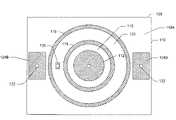
- a submount 100 for mounting an LED chip 114includes a substrate 110 having an upper surface 110 A and a lower surface 110 B.
- the substrate 110may include a printed circuit board (PCB), an aluminum block, an alumina, aluminum nitride or silicon wafer, or any other suitable substrate material, such as T-Clad thermal clad insulated substrate material, available from The Bergquist Company of Chanhassen, Minn.
- a plurality of patterned metal featuresare formed on the upper surface 110 A of the substrate 110 .
- the patterned metal featuresmay include, for example, a die attach pad 112 , a wire bond pad 120 , a first meniscus control feature 116 , a second meniscus control feature 118 , and/or electrodes 124 .
- the conductive features on the top surface 110 A of substrate 110may be formed, for example, using a plating process.
- a plating processmay be used to plate a thin or thick metallic film on a substrate. In a typical plating process, a titanium adhesion layer and a copper seed are sequentially sputtered onto a substrate. Then, approximately 75 microns of copper are plated onto the copper seed.
- a plating processmay be utilized to form a metal film having a characteristic structure.
- a deposited metal filmmay be patterned using standard lithographic processes to produce metal films on the substrate having desired patters.
- the adhesion layer and seedmay be sputtered using, for example, a metal mask to form a desired pattern.
- a plating processmay also be used to form conductive metal vias through a substrate.
- the first and second meniscus control features 116 , 118maybe formed of a material different from the die attach pad 112 and/or the wirebond pad 120 .
- the meniscus control features 116 , 118 , 210may comprise a polymer such as a solder mask material including for example polyimide.
- a polymer such as polyimidemay provide a suitable material for use as a meniscus control feature since polyimide may have a high surface energy, which may provide better meniscus control properties.
- the conductive viasmay provide electrical contact between features formed on opposite sides of a substrate. Accordingly, respective conductive features formed on the upper surface of substrate 110 may be formed of the same material.
- the conductive featuresmay include copper deposited using a plating process.
- some featuresmay include additional metals.
- the die attach pad 112may be plated and/or coated with additional metals and/or other materials to make the die attach pad 112 more suitable for mounting an LED chip 114 .
- the die attach pad 112may be plated with additional layers such as, for example, additional adhesive, bonding, reflector and/or barrier layers (not shown).
- the die attach pad 112may be generally centrally located on the upper surface 110 A of the substrate 110 .
- the die attach pad 112may be generally circular in shape, or may have any other desired shape.
- the first meniscus control feature 116 formed on the substrate 110surrounds the die attach pad 112 and defines a first encapsulant region 115 on the upper surface 110 A of the substrate 110 within the periphery of the first meniscus control feature 116 .
- the second meniscus control feature 118surrounds the first encapsulant region 115 and defines a second encapsulant region 125 on the upper surface 110 A of the substrate 110 within the periphery of the second meniscus control feature 118 .
- the second encapsulant region 125may enclose and encompass the first encapsulant region 115 .
- the wirebond pad 120may be formed on the upper surface 110 A of substrate 110 within the first encapsulant region 115 and/or within the second encapsulant region 125 .
- One or more of the electrodes 124may also be formed on the upper surface 110 A of the substrate 110 .
- one or more lower electrodes 126may be formed on a lower surface 110 B of the substrate 110 as shown in FIG. 2A .
- One or more conductive vias 122may connect one or more of the lower electrodes 126 A, 126 B to various features on the upper surface 110 A of the substrate 110 .
- one of the conductive vias 122may electrically connect the electrodes 124 A, 124 B with respective lower electrodes 126 A, 126 B.
- one of the conductive vias 122may electrically connect the wire bond pad 120 with the lower electrode 126 A, and/or one of the conductive vias 122 may electrically connect the die attach pad 112 with the lower electrode 126 B.
- an LED chip 114 mounted on the die attach pad 112may be covered with an encapsulant material 130 .
- the encapsulant material 130may be dispensed onto the upper surface 110 A of the substrate 110 using, for example, an automated dispense system, as described more fully below.
- the encapsulant material 130may include a liquid silicone, an epoxy resin, and/or another suitable optical encapsulant material.
- the encapsulant material 130may include a wavelength conversion material, such as a phosphor and/or a nanocrystal, therein to convert a wavelength of light emitted by the LED chip 114 to a second wavelength.
- the first encapsulant material 130is dispensed within the first encapsulant region 115 defined by the first meniscus control feature 116 .
- the first encapsulant material 130may form a liquid meniscus (i.e. a curved bubble or dome) over the LED chip 114 .
- Surface tension in the liquid encapsulant material 130may cause it to cling to the first meniscus control feature 116 .
- the liquid encapsulant material 130may cling to a corner 116 a of the first meniscus control feature 116 and/or a surface of the first meniscus control feature 116 .
- the encapsulant material 130may cling to a corner 116 a of the meniscus control feature 116 that is farthest from the center of the dome of the encapsulant material 130 .
- the dispensed first encapsulant material 130may be cured, for example, by heating at an appropriate temperature for an appropriate time, to cause the first encapsulant material to harden over the LED chip 114 .
- a cure stepmay include a full and/or partial curing of an encapsulant material. A full cure may cause the liquid encapsulant material to harden completely, while a partial cure may cause the liquid encapsulant to only partially harden.
- a full curemay be performed after some or all subsequent dispenses have been performed.
- a wirebond connection 128may be formed between the LED chip 114 and the wire bond pad 120 .
- the wirebond connection 128may be made before dispense of the first encapsulant material 130 , so that when it is cured, the first encapsulant material 130 may harden around the wirebond connection 128 .
- a second encapsulant material 140may be dispensed within the second encapsulant region 125 of the upper surface 110 A of the substrate 110 , i.e. over the cured first encapsulant material 130 .
- the second encapsulant material 140may form a meniscus dome over the second encapsulant region 125 .
- the second encapsulant material 140may cling to a corner 118 a or a surface of the second meniscus control feature 118 due, for example, to surface tension in the encapsulant material 140 .
- the second encapsulant material 140may include a clear silicone gel, an epoxy resin, and/or any other optically clear encapsulant material.
- the dispensed second encapsulant material 140may be cured, for example, by heating the encapsulant material to a suitable temperature for a suitable time period, to cause the second encapsulant material 140 to harden.
- the second encapsulant material 140may accordingly form an optically transparent lens over the cured first encapsulant material 130 and the LED chip 114 .
- An LED chip 114 packaged in accordance with some embodiments of the inventionmay approximate an ideal point source of light.
- the design of secondary optics (not shown) for the packaged LEDmay be simplified.
- light output of the packaged LEDmay be improved as optical losses associated with mounting an LED chip inside a reflector cup may be avoided when an LED chip 114 is packaged in accordance with some embodiments of the invention.
- a submount 200 for mounting an LED chip 114includes a substrate 110 having an upper surface 110 A and a lower surface 110 B.
- a plurality of metal featuresare formed on the upper surface 110 A of the substrate 110 , for example, by a plating process.
- the submount 200may include a die attach pad 112 , a wire bond pad 120 , a first meniscus control feature 116 defining a first encapsulant region 115 , and a second meniscus control feature 118 defining a second encapsulant region 125 .
- embodiments of the inventionmay further include a third meniscus control feature 210 formed within the first encapsulant region 115 surrounding the die attach pad 112 and defining a third encapsulant region 215 .
- the first meniscus control feature 116 and the third meniscus control feature 210define a region 225 within the first encapsulant region 115 surrounding the third encapsulant region 215 .
- the meniscus control features 116 , 118 , 210may include a material different from the die attach pad 112 and the wirebond pad 120 .
- the meniscus control features 116 , 118 , 210may include a polymer such as polyimide.
- the first meniscus control feature 116 , second meniscus control feature 118 and third meniscus control feature 210may be generally circular in shape. Accordingly, the region 225 defined between the first meniscus control feature 116 and the third meniscus control feature 210 may be generally annular or ring-shaped.
- An encapsulant materialmay be deposited in an annular region 225 in for example, a circular pattern, by moving a dispensing needle in a circular motion as discussed in more detail below. In this manner, the desired pattern may be “drawn” onto the substrate with the needle.
- first, second and third meniscus control features 116 , 118 , 210may be other shapes.
- the meniscus control featurescould be generally oval and/or rectangular in shape.
- the meniscus control featuresmay be continuous features formed on the upper surface 110 A of the substrate 110 . If the meniscus control features are not continuous features, encapsulant material dispensed within regions defined by the meniscus control features may be more likely to fail to be confined within a desired region.
- a first encapsulant material 230may be dispensed within the region 225 defined by the first meniscus control feature 116 and the third meniscus control feature 210 .
- the first encapsulant material 230may cling to a corner 116 a of the first meniscus control feature 116 and a corner 210 a of the third meniscus control feature 210 that are distant from the center of region 225 . That is, when it is dispensed, the encapsulant material 230 may flow outward until it reaches an outer corner of the respective first and third meniscus control features 116 , 210 where it may be held in place, for example, by surface tension.
- the dispensed first encapsulant material 230may be cured, for example, by heating the encapsulant material for a suitable period of time at a suitable temperature, by allowing the dispensed encapsulant to sit for a suitable period of time at room temperature, by exposure to UV light, and/or with the aid of a catalyst.
- the cured first encapsulant material 230may thereby form a hardened ring surrounding the third encapsulant region 215 including the die attach pad 112 and the LED chip 114 mounted thereon.
- the first encapsulant material 230may define a cavity 220 surrounding the LED chip 114 .
- the height of the first encapsulant material 230may be greater than, equal to, or less than the height of the mounted LED chip 114 on the die attach pad 112 .
- a second encapsulant material 240may be dispensed into the cavity 220 defined by the first encapsulant material 230 .
- the second encapsulant material 240may include a wavelength conversion material, such as a phosphor and/or nanocrystal.
- the dispensed second encapsulant material 240may be cured in the manner described above.
- a third encapsulant material 250may be dispensed within the second encapsulant region 125 (i.e. over the first encapsulant material 230 and the second encapsulant material 240 ).
- the third encapsulant material 250may form a domed meniscus lens above the LED chip 114 , the first encapsulant material 230 and the second encapsulant material 240 .
- the dispensed third encapsulant material 250may be cured as described above.
- FIGS. 4A-4CFurther embodiments of the invention are illustrated in FIGS. 4A-4C .
- a single patterned surface feature 308provides the first meniscus control feature 116 at a first corner 308 a of the feature 308 and the third meniscus control feature 210 at the opposite corner 308 b of the feature 308 .
- the first corner of the feature 308may correspond to an outer circumference of a generally ring shaped feature.
- the second corner of the feature 308may correspond to an inner circumference of the feature 308 .
- the first encapsulant material 230may be dispensed by dispensing an encapsulant material above the feature 308 .
- the encapsulant material 230may flow outward on the feature 308 and cling to the inner and outer peripheral edges of the feature 308 (i.e., the first meniscus control feature 116 and the third meniscus control feature 210 , respectively).
- the second encapsulant material 240may be dispensed within the cavity 220 defined by first encapsulant material 230 .
- the third encapsulant material 250may be dispensed within the second encapsulant region 125 to form a dome-shaped meniscus lens above the LED chip 114 .
- some embodiments according to the inventionmay include one or more surface features 310 formed on the upper surface 110 A of substrate 110 between the first meniscus control feature 116 and the second meniscus control feature 118 .
- the surface features 310may include a plurality of patterned features arranged to overlap one another such that an arbitrary path 325 extending in a radial direction from the first meniscus control feature 116 to the second meniscus control feature 118 is interrupted by at least one surface feature 310 .
- the surface features 310may perform a number of functions.
- the surface features 310may provide a patterned feature on the upper surface 110 A of the substrate 110 to which an encapsulant material dispensed over the surface may grip, which may provide a better, more mechanically robust connection between the encapsulant material and the upper surface 110 A of the substrate 110 .
- the surface features 310may slow the flow of liquid encapsulant material across the surface of the region in which the surface features 310 are formed so that, for example, the liquid encapsulant material may be more likely to cling to a meniscus control feature as desired.
- an encapsulant materialwhen dispensed within the second encapsulant region 125 , if the material flows too quickly within region 125 , it may flow over the meniscus control feature 118 and out of the second encapsulant region 125 . However, when the flow of the second encapsulant material 140 is limited by the surface features 310 , the encapsulant material may more reliably cling to the second meniscus control feature 118 .
- the surface features 310are illustrated between the first meniscus control feature 116 and the second meniscus control feature 118 in FIG. 5 .
- the surface features 310could be formed in any region of the upper surface 110 A on which encapsulant material is to be dispensed Moreover, it will be understood that while the surface features 310 are illustrated as being discontinuous, the surface features 310 could be continuous provided they are small enough or formed with an appropriate shape and/or thickness such that encapsulant material will not undesirably cling to an edge or surface of the surface feature 310 .
- one or more meniscus extension features 300 A, 300 Bmay be formed on the upper surface 110 A of substrate 110 outside the second meniscus control feature 118 .
- the meniscus extension features 300 A, 300 Bmay have peripheral geometries different from the peripheral geometry of the second meniscus control feature 118 .
- the second meniscus control feature 118has a generally circular shape, while the meniscus extension features 300 A, 300 B have generally elliptical shapes with sequentially increasing axis lengths and eccentricities (i.e. increasing ratios of major axis length to minor axis length).
- the shape of the lens formed by the second encapsulant material 140may be modified by dispensing additional encapsulant material within the regions defined by the encapsulant extension features 300 A and 300 B.
- the ultimate shape of the lens covering the LED chip 114may be determined by the shape of the encapsulant extension features 300 A, 300 B, as well as the number of dispense/cure steps employed.
- Multiple encapsulant extension features 300 A, 300 Bmay be employed to gradually increase the size and/or change the shape of the lens while limiting the amount of encapsulant material that needs to be dispensed in any given dispense/cure cycle. Although two encapsulant extension features 300 A, 300 B are illustrated in FIGS.
- the surface features 310 and/or the meniscus extension features 300 A, 300 Bmay include patterned metal films that may be formed concurrently with the formation of the die attach pad 112 .
- the surface features 310 and/or the meniscus extension features 300 A, 300 Bmay include a different material such as a polymer such as polyimide.
- a quantity of encapsulant material 330 Amay be dispensed within the region 315 A bounded by the encapsulant extension feature 300 A.
- the encapsulant material 330 Amay be cured to form a hardened dome 332 A having a different peripheral shape than the dome formed by the second encapsulant material 140 .
- a second quantity of the encapsulant material 330 Bmay be dispensed within the region 315 B defined by the encapsulant extension feature 300 B.
- the dispensed encapsulant material 330 Bmay be cured to form a hardened lens 332 B over the LED chip 114 having a different peripheral shape than second encapsulant material 140 or the dome 332 A. This process may be repeated as desired until a desired shape of meniscus lens is formed above the LED chip 114 .
- FIG. 6Cis a perspective view of a resulting LED package 350 .
- the encapsulant extension regionsmay have shapes other than circular or oval.
- the encapsulant extension features 300 A, 300 Bmay have peripheral shapes that are generally square and/or rectangular. Other shapes are possible and may be used to produce different shaped lenses as desired.
- the ability to deliver small volumes of fluids accuratelymay be important in the manufacture of packaged LEDs according to the invention.
- a variety of different fabrication operations in the semiconductor industryutilize sub-microliter control of fluid dispensing. Such uses may utilize accurate, repeatable and rapid dispensing of precise amounts of fluids. Inaccurate dispensing may adversely impact the yield of a fabrication process.
- a microliter quantity of an encapsulant materialsuch as liquid silicone gel
- an encapsulant materialsuch as liquid silicone gel
- a bead of the materialis typically formed on a dispensing needle and then contacted to surfaces of the substrate 110 and/or the light-emitting device 114 .
- the surface tension between the encapsulant material and surfaces on the substrate 110 and gravitymay cause the encapsulant material to tear-off from the dispensing needle and remain on the substrate 110 .
- the encapsulant materialmay be dispensed in a desired pattern, for example, a circular pattern, by moving the needle in a circular motion after contacting the bead to the surface of the substrate. In this manner, the desired pattern may be “drawn” onto the substrate with the needle.
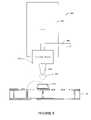
- FIG. 8A system 400 for dispensing an encapsulant material for use in packaging a light emitting device according to some embodiments of the invention is illustrated in FIG. 8 .
- the system 400includes a frame 402 , which may be attached to an articulated arm (not shown) configured to controllably move the frame 402 in the X, Y, and Z dimensions.
- a needle mount member 404is mounted on the frame 402 , and an encapsulant supply line 406 is coupled to the needle mount member 404 for supplying a quantity of encapsulant material to a hollow dispensing needle 408 mounted on the needle mount member 404 .
- a bead of encapsulant 410may be formed at the tip of the dispensing needle 408 .
- the bead of encapsulant 410may be dispensed onto the substrate 110 and/or the LED chip 114 by contacting the bead 410 to a surface of the substrate 110 and/or the LED chip 114 .
- the shape of the dispensed encapsulantmay be controlled by moving the frame 402 in the X and Y dimensions as the encapsulant is being dispensed.
- the encapsulantmay be effectively dispensed into an annular region by moving the frame in a circular pattern after contacting the bead 410 to a surface of the substrate 110 within the annular region.
- the viscosity and/or other properties of the material used for a dispensemay be selected such that, for example, wetting occurs without bubble formation.
- coatingsmay be applied to surfaces contacted by the dispensed material to speed/retard the wetting rate. For example, using certain known cleaning procedures that leave microscopic residue, selected surfaces may be treated and, thus, used to engineer the dynamics of the wetting action.
- the dispensed encapsulant materialmay flow in a manner that could cause bubbles to form therein.
- the encapsulant materialmay move or “wick” more rapidly around the sidewalls of the LED chip 114 faster than over the top of the LED chip 114 .
- a bubblecould be trapped on a side of the LED 114 opposite from the side where the encapsulant material is dispensed when the side-flowing encapsulant material meets, and then encapsulant material flows over the top of the LED chip 114 .
- the encapsulantwhen encapsulant material is dispensed into an encapsulant region including the LED chip 114 , such as, for example, the encapsulant region 115 illustrated in FIG. 2B , the encapsulant may be pre-dispensed in a first dispense portion adjacent the LED chip 114 selected to substantially cover the LED chip 114 and a second dispense portion selected to fill the encapsulant region 115 .
- the quantity of the first portion of dispensed encapsulant materialmay be selected to reduce or prevent the risk of forming bubbles around the LED chip 114 .
- substantially covering the LED chip 114refers to covering enough of the structure of the LED chip 114 so that such a bubble will not generally result when the remaining portion of the encapsulant material dispensed. After the initially dispensed portion of encapsulant material is allowed to settle, the second portion of the encapsulant material may be dispensed into the encapsulant region.
- FIGS. 9-11Methods of forming LED submounts and packaged LEDs according to some embodiments of the invention are further illustrated in FIGS. 9-11 .
- the methods illustrated in FIGS. 9-11are described with reference to the embodiments illustrated in FIGS. 2A-8 above. As illustrated in FIG.
- some methods 500 of forming an LED submountincludes depositing a metal layer on a substrate 110 (block 510 ); and patterning the metal layer to form a die attach pad 112 , a first meniscus control feature 116 surrounding the die attach pad 112 and defining a first encapsulant region 115 of the upper surface of the substrate 110 , and a second meniscus control feature 118 surrounding the first encapsulant region 115 and defining a second encapsulant region 125 of the upper surface of the substrate 110 (block 520 ).
- methods 600may include depositing a metal layer on a substrate 110 (block 610 ) and patterning the metal layer to form a die attach pad 112 , a first meniscus control feature 116 , and a second meniscus control feature 118 (block 620 ).
- the first meniscus control featuresurrounds the die attach pad 112 and defines a first encapsulant region 115 of the upper surface of the substrate 110
- the second meniscus control feature 118surrounds the first encapsulant region 115 and defines a second encapsulant region 125 of the upper surface of the substrate 110 .
- the method 600further includes mounting an LED chip 114 on the die attach pad 112 on the substrate 110 (block 630 ).
- a first encapsulant material 130is then dispensed onto the substrate 110 and the LED chip 114 within the first encapsulant region 115 (block 640 ), and the first encapsulant material 130 is cured (block 650 ).
- a second encapsulant material 140is dispensed onto the substrate 110 within the second encapsulant region 125 (block 660 ), and the second encapsulant material 140 is cured (block 670 ).
- patterning the metal layerincludes patterning the metal layer to form a wirebond pad 120 within the second encapsulant region 125 . In some embodiments, the method further includes forming a wirebond connection between the LED chip 114 and the wirebond pad 120 .
- some embodiments of the inventioninclude pre-dispensing a quantity of encapsulant material adjacent the LED chip 114 prior to dispensing the first encapsulant material 130 . Moreover, a sufficient quantity of the first encapsulant material 130 may be pre-dispensed to substantially cover the LED chip 114 .
- the first encapsulant material 130includes a wavelength conversion material such as a phosphor or a nanocrystal.
- Patterning the metal layermay further include forming at least one surface feature 300 between the first and second meniscus control features 118 .
- the surface features 300may help the encapsulant material adhere to the surface 110 A of the substrate 110 and/or cling to the meniscus control features 116 , 118 .
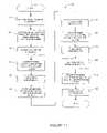
- FIG. 11further methods 700 of forming a packaged LED according to some embodiments of the invention are illustrated that include depositing a metal layer on a substrate 110 (block 710 ).
- the metal layeris patterned to form a die attach pad 112 , a first meniscus control feature 116 , a second meniscus control feature 118 and a third meniscus control feature 210 (block 720 ).
- the first meniscus control feature 116may surround the die attach pad 112 and define a first encapsulant region 115 of the upper surface of the substrate 110 .
- the second meniscus control feature 118may surround the first encapsulant region 115 and define a second encapsulant region 125 of the upper surface of the substrate 110 .
- the third meniscus control feature 210is formed within the first encapsulant region 115 and may surround the die attach pad 112 to thereby define a third encapsulant region 215 within the first encapsulant region 115 .
- the first meniscus control feature 116 and the third meniscus control feature 210define a region 225 in the first encapsulant region 115 surrounding the third encapsulant region 215 . It will be understood that for a feature to “surround” a region, the feature need not be continuously formed around the region. Although the figures illustrate continuous features, it may be possible for a meniscus control feature to include gaps or voids therein which do not affect the meniscus control function of the feature.
- the methods 700may further include mounting an LED chip 114 on the die attach pad 112 (block 730 ) and dispensing a first encapsulant material 230 within the region 225 in the first encapsulant region 115 defined by the first meniscus control feature 116 and the third meniscus control feature 210 (block 740 ).
- the dispensed first encapsulant material 230is cured (block 750 ) and a second encapsulant material 240 is dispensed onto the substrate 110 within the third encapsulant region 215 (block 760 ).
- the dispensed second encapsulant material 240may be cured (block 770 ).
- the methods 700may further include dispensing a third encapsulant material 250 within the second encapsulant region 125 (block 780 ), and curing the third encapsulant material 250 (block 790 ).
- the dispensed first encapsulant material 230may define a cavity 220 around the LED chip 114
- dispensing the second encapsulant material 240may include dispensing the second encapsulant material 240 into the cavity 220 around the LED chip 114 after curing the first encapsulant material 230 .
- the first encapsulant material 230 , the second encapsulant material 240 and/or the third encapsulant 230 materialmay include a wavelength conversion material.
- Some methods of the inventioninclude forming a meniscus extension feature 300 outside the second encapsulant region 125 surrounding the second encapsulant region 125 and defining a encapsulant extension area 315 of the upper surface of the substrate 110 (block 800 ), and dispensing a fourth encapsulant material 330 in the encapsulant extension area 315 after curing the second encapsulant material 140 (block 810 ) and curing the fourth encapsulant material 330 (block 820 ).
- the encapsulant extension area 315may have a peripheral shape that is different from a peripheral shape of the second encapsulant region 125 .
- the encapsulant extension area 315may have a peripheral shape that is oval, circular or generally square or rectangular.
Landscapes
- Led Device Packages (AREA)
- Structures Or Materials For Encapsulating Or Coating Semiconductor Devices Or Solid State Devices (AREA)
Abstract
Description
Claims (19)
Priority Applications (12)
| Application Number | Priority Date | Filing Date | Title |
|---|---|---|---|
| US11/197,096US7365371B2 (en) | 2005-08-04 | 2005-08-04 | Packages for semiconductor light emitting devices utilizing dispensed encapsulants |
| KR1020137027934AKR101455022B1 (en) | 2005-08-04 | 2005-09-14 | Packages for semiconductor light emitting devices utilizing dispensed encapsulants and methods of packaging the same |
| JP2008524949AJP5220603B2 (en) | 2005-08-04 | 2005-09-14 | Method for packaging a semiconductor light emitting device using a distributed encapsulant |
| DE112005003652TDE112005003652T5 (en) | 2005-08-04 | 2005-09-14 | Semiconductor light emitting device packages using dispensed encapsulants and methods of encapsulating them |
| CN201110201851.9ACN102280567B (en) | 2005-08-04 | 2005-09-14 | Packages for semiconductor light emitting devices utilizing dispensed encapsulants and methods of packaging the same |
| KR1020087005266AKR101365875B1 (en) | 2005-08-04 | 2005-09-14 | Packages for semiconductor light emitting devices utilizing dispensed encapsulants and methods of packaging the same |
| PCT/US2005/033057WO2007018560A1 (en) | 2005-08-04 | 2005-09-14 | Packages for semiconductor light emitting devices utilizing dispensed encapsulants and methods of packaging the same |
| CN2005800517483ACN101278410B (en) | 2005-08-04 | 2005-09-14 | Encapsulation of semiconductor light emitting device using dispensed encapsulant and encapsulation method thereof |
| US12/100,647US7834375B2 (en) | 2005-08-04 | 2008-04-10 | Submounts for semiconductor light emitting devices and methods of forming packaged light emitting devices including dispensed encapsulants |
| US12/938,815US8202745B2 (en) | 2005-08-04 | 2010-11-03 | Submounts for semiconductor light emitting devices and methods of forming packaged light emitting devices including dispensed encapsulants |
| US13/149,197US8835952B2 (en) | 2005-08-04 | 2011-05-31 | Submounts for semiconductor light emitting devices and methods of forming packaged light emitting devices including dispensed encapsulants |
| JP2012223101AJP5542890B2 (en) | 2005-08-04 | 2012-10-05 | Package for semiconductor light emitting device using distributed sealant and method for packaging the same |
Applications Claiming Priority (1)
| Application Number | Priority Date | Filing Date | Title |
|---|---|---|---|
| US11/197,096US7365371B2 (en) | 2005-08-04 | 2005-08-04 | Packages for semiconductor light emitting devices utilizing dispensed encapsulants |
Related Parent Applications (1)
| Application Number | Title | Priority Date | Filing Date |
|---|---|---|---|
| US12/624,885Continuation-In-PartUS7952115B2 (en) | 2005-08-04 | 2009-11-24 | Packaged light emitting devices including multiple index lenses and methods of fabricating the same |
Related Child Applications (1)
| Application Number | Title | Priority Date | Filing Date |
|---|---|---|---|
| US12/100,647DivisionUS7834375B2 (en) | 2005-08-04 | 2008-04-10 | Submounts for semiconductor light emitting devices and methods of forming packaged light emitting devices including dispensed encapsulants |
Publications (2)
| Publication Number | Publication Date |
|---|---|
| US20070029569A1 US20070029569A1 (en) | 2007-02-08 |
| US7365371B2true US7365371B2 (en) | 2008-04-29 |
Family
ID=36283075
Family Applications (3)
| Application Number | Title | Priority Date | Filing Date |
|---|---|---|---|
| US11/197,096Active2025-11-26US7365371B2 (en) | 2005-08-04 | 2005-08-04 | Packages for semiconductor light emitting devices utilizing dispensed encapsulants |
| US12/100,647Active2025-10-20US7834375B2 (en) | 2005-08-04 | 2008-04-10 | Submounts for semiconductor light emitting devices and methods of forming packaged light emitting devices including dispensed encapsulants |
| US12/938,815Expired - LifetimeUS8202745B2 (en) | 2005-08-04 | 2010-11-03 | Submounts for semiconductor light emitting devices and methods of forming packaged light emitting devices including dispensed encapsulants |
Family Applications After (2)
| Application Number | Title | Priority Date | Filing Date |
|---|---|---|---|
| US12/100,647Active2025-10-20US7834375B2 (en) | 2005-08-04 | 2008-04-10 | Submounts for semiconductor light emitting devices and methods of forming packaged light emitting devices including dispensed encapsulants |
| US12/938,815Expired - LifetimeUS8202745B2 (en) | 2005-08-04 | 2010-11-03 | Submounts for semiconductor light emitting devices and methods of forming packaged light emitting devices including dispensed encapsulants |
Country Status (6)
| Country | Link |
|---|---|
| US (3) | US7365371B2 (en) |
| JP (2) | JP5220603B2 (en) |
| KR (2) | KR101455022B1 (en) |
| CN (2) | CN101278410B (en) |
| DE (1) | DE112005003652T5 (en) |
| WO (1) | WO2007018560A1 (en) |
Cited By (31)
| Publication number | Priority date | Publication date | Assignee | Title |
|---|---|---|---|---|
| US20080191237A1 (en)* | 2005-08-04 | 2008-08-14 | Cree, Inc. | Submounts for semiconductor light emitting devices and methods of forming packaged light emitting devices including dispensed encapsulants |
| US20080238702A1 (en)* | 2007-03-30 | 2008-10-02 | Innolux Display Corp. | Electrostatic discharge protection device with phosphors and method of fabricating the same |
| US20090090926A1 (en)* | 2007-10-09 | 2009-04-09 | Foxsemicon Integrated Technology, Inc. | Solid state light emitting device |
| US20090141492A1 (en)* | 2006-01-26 | 2009-06-04 | Sony Corporation | Light source apparatus, and display apparatus |
| US20100038672A1 (en)* | 2007-04-02 | 2010-02-18 | Lg Innotek Co., Ltd. | Light emitting device and method for fabricating the same |
| US20100066947A1 (en)* | 2006-11-15 | 2010-03-18 | Hathaway Kevin J | High output led based illuminator that replaces ccfls for lcd backlights |
| US7772604B2 (en) | 2006-01-05 | 2010-08-10 | Illumitex | Separate optical device for directing light from an LED |
| US7789531B2 (en) | 2006-10-02 | 2010-09-07 | Illumitex, Inc. | LED system and method |
| US7829358B2 (en) | 2008-02-08 | 2010-11-09 | Illumitex, Inc. | System and method for emitter layer shaping |
| US20110001161A1 (en)* | 2008-07-21 | 2011-01-06 | Jun Suk Park | Light emitting diode and method of manufacturing the same, and light emitting device and method of manufacturing the light emitting device |
| US20110062483A1 (en)* | 2009-09-15 | 2011-03-17 | Wenbing Wang | Light-emitting diode |
| US20110085352A1 (en)* | 2008-05-30 | 2011-04-14 | Shin Ito | Light emitting device, surface light source, liquid crystal display device, and method for manufacturing light emitting device |
| US8008676B2 (en) | 2006-05-26 | 2011-08-30 | Cree, Inc. | Solid state light emitting device and method of making same |
| US8096671B1 (en) | 2009-04-06 | 2012-01-17 | Nmera, Llc | Light emitting diode illumination system |
| US8115217B2 (en) | 2008-12-11 | 2012-02-14 | Illumitex, Inc. | Systems and methods for packaging light-emitting diode devices |
| WO2012099791A3 (en)* | 2011-01-21 | 2012-11-08 | Cree, Inc. | Light emitting diodes with low junction temperature |
| US20130026507A1 (en)* | 2009-07-06 | 2013-01-31 | Paragon Semiconductor Lighting Technology Co., Ltd. | Multichip package structure and method of manufacturing the same |
| CN103003965A (en)* | 2010-07-16 | 2013-03-27 | 欧司朗光电半导体有限公司 | Carrier with solder barrier against solder creep for semiconductor chips, electronic component with carrier and optoelectronic component with carrier |
| US8431942B2 (en) | 2010-05-07 | 2013-04-30 | Koninklijke Philips Electronics N.V. | LED package with a rounded square lens |
| US8449128B2 (en) | 2009-08-20 | 2013-05-28 | Illumitex, Inc. | System and method for a lens and phosphor layer |
| US20130181247A1 (en)* | 2010-07-22 | 2013-07-18 | Osram Opto Semiconductors Gmbh | Semiconductor Component and Method for Producing a Semiconductor Component |
| US20130217152A1 (en)* | 2012-02-20 | 2013-08-22 | Jeffrey D. Mullen | Systems and methods for flexible components for powered cards and devices |
| US8585253B2 (en) | 2009-08-20 | 2013-11-19 | Illumitex, Inc. | System and method for color mixing lens array |
| US20140001505A1 (en)* | 2012-06-29 | 2014-01-02 | Advanced Optoelectronic Technology, Inc. | Light emitting diode package with lens and method for manufacturing the same |
| US8835952B2 (en) | 2005-08-04 | 2014-09-16 | Cree, Inc. | Submounts for semiconductor light emitting devices and methods of forming packaged light emitting devices including dispensed encapsulants |
| US20150179891A1 (en)* | 2007-12-28 | 2015-06-25 | Nichia Corporation | Light emitting device |
| US9443903B2 (en) | 2006-06-30 | 2016-09-13 | Cree, Inc. | Low temperature high strength metal stack for die attachment |
| US20170040496A1 (en)* | 2013-06-28 | 2017-02-09 | Koninklijke Philips N.V. | Light emitting diode device |
| US10043960B2 (en)* | 2011-11-15 | 2018-08-07 | Cree, Inc. | Light emitting diode (LED) packages and related methods |
| US10147853B2 (en) | 2011-03-18 | 2018-12-04 | Cree, Inc. | Encapsulant with index matched thixotropic agent |
| US11824148B2 (en) | 2018-02-26 | 2023-11-21 | Elphoton Inc. | Semiconductor light emitting devices and method of manufacturing the same |
Families Citing this family (163)
| Publication number | Priority date | Publication date | Assignee | Title |
|---|---|---|---|---|
| US7915085B2 (en) | 2003-09-18 | 2011-03-29 | Cree, Inc. | Molded chip fabrication method |
| US7217583B2 (en) | 2004-09-21 | 2007-05-15 | Cree, Inc. | Methods of coating semiconductor light emitting elements by evaporating solvent from a suspension |
| TWI248218B (en)* | 2004-12-31 | 2006-01-21 | Ind Tech Res Inst | Light-emitting diode package structure and fabrication method thereof |
| KR20070045462A (en)* | 2005-10-27 | 2007-05-02 | 엘지이노텍 주식회사 | Light emitting diode package |
| JP4417906B2 (en)* | 2005-12-16 | 2010-02-17 | 株式会社東芝 | Light emitting device and manufacturing method thereof |
| WO2007075742A2 (en) | 2005-12-21 | 2007-07-05 | Cree Led Lighting Solutions, Inc. | Lighting device |
| JP4996101B2 (en)* | 2006-02-02 | 2012-08-08 | 新光電気工業株式会社 | Semiconductor device and manufacturing method of semiconductor device |
| US8969908B2 (en)* | 2006-04-04 | 2015-03-03 | Cree, Inc. | Uniform emission LED package |
| US9780268B2 (en) | 2006-04-04 | 2017-10-03 | Cree, Inc. | Submount based surface mount device (SMD) light emitter components and methods |
| US7863639B2 (en)* | 2006-04-12 | 2011-01-04 | Semileds Optoelectronics Co. Ltd. | Light-emitting diode lamp with low thermal resistance |
| USD555114S1 (en)* | 2006-04-12 | 2007-11-13 | Semi-Photonics Co., Ltd. | Light emitting diode |
| USD555113S1 (en)* | 2006-04-12 | 2007-11-13 | Semi-Photonics Co., Ltd. | Opto-electronic device |
| US8373195B2 (en) | 2006-04-12 | 2013-02-12 | SemiLEDs Optoelectronics Co., Ltd. | Light-emitting diode lamp with low thermal resistance |
| KR100731678B1 (en)* | 2006-05-08 | 2007-06-22 | 서울반도체 주식회사 | Chip type light emitting diode package and light emitting device having the same |
| USD571315S1 (en)* | 2006-06-19 | 2008-06-17 | Avago Technologies Ecbu Ip (Singapore) Pte Ltd | Light emitting diode |
| USD576966S1 (en) | 2006-06-26 | 2008-09-16 | Avago Technologies General Ip (Singapore) Pte Ltd. | Light emitting diode |
| US7909482B2 (en) | 2006-08-21 | 2011-03-22 | Innotec Corporation | Electrical device having boardless electrical component mounting arrangement |
| EP1914809A1 (en)* | 2006-10-20 | 2008-04-23 | Tridonic Optoelectronics GmbH | Cover for optoelectronic components |
| US10295147B2 (en) | 2006-11-09 | 2019-05-21 | Cree, Inc. | LED array and method for fabricating same |
| US9024349B2 (en) | 2007-01-22 | 2015-05-05 | Cree, Inc. | Wafer level phosphor coating method and devices fabricated utilizing method |
| US9159888B2 (en) | 2007-01-22 | 2015-10-13 | Cree, Inc. | Wafer level phosphor coating method and devices fabricated utilizing method |
| US8330176B2 (en) | 2007-02-13 | 2012-12-11 | 3M Innovative Properties Company | LED devices having lenses and methods of making same |
| US9944031B2 (en)* | 2007-02-13 | 2018-04-17 | 3M Innovative Properties Company | Molded optical articles and methods of making same |
| DE102007021904A1 (en)* | 2007-02-28 | 2008-09-04 | Osram Opto Semiconductors Gmbh | Housing body for opto-electronic component, has main surface with surface area and another surface area, and both surface areas are adjoined together by outer edge |
| US8408773B2 (en)* | 2007-03-19 | 2013-04-02 | Innotec Corporation | Light for vehicles |
| CN101663750B (en)* | 2007-03-23 | 2011-06-29 | 富士通株式会社 | RFID tag and manufacturing method thereof |
| TW200900628A (en)* | 2007-06-28 | 2009-01-01 | Wen-Chin Shiau | Manufacturing method of heat-dissipating structure of high-power LED lamp seat and product thereof |
| US20090065792A1 (en)* | 2007-09-07 | 2009-03-12 | 3M Innovative Properties Company | Method of making an led device having a dome lens |
| WO2009076579A2 (en)* | 2007-12-12 | 2009-06-18 | Innotec Corporation | Overmolded circuit board and method |
| KR100998009B1 (en)* | 2008-03-12 | 2010-12-03 | 삼성엘이디 주식회사 | Light emitting diode package and manufacturing method thereof |
| US8637883B2 (en)* | 2008-03-19 | 2014-01-28 | Cree, Inc. | Low index spacer layer in LED devices |
| US7980728B2 (en)* | 2008-05-27 | 2011-07-19 | Abl Ip Holding Llc | Solid state lighting using light transmissive solid in or forming optical integrating volume |
| KR101039496B1 (en)* | 2008-06-17 | 2011-06-08 | 한국광기술원 | Light emitting diode package having a domed encapsulation layer and a method of manufacturing the same |
| JP2010003994A (en)* | 2008-06-23 | 2010-01-07 | Sharp Corp | Lighting device, backlight device, and method of manufacturing lighting device |
| US8680550B2 (en)* | 2008-07-03 | 2014-03-25 | Samsung Electronics Co., Ltd. | Wavelength-converting light emitting diode (LED) chip and LED device equipped with chip |
| JP2010040894A (en)* | 2008-08-07 | 2010-02-18 | Rohm Co Ltd | Semiconductor device and manufacturing method of semiconductor device |
| WO2010021346A1 (en)* | 2008-08-20 | 2010-02-25 | 三菱化学株式会社 | Semiconductor light emitting device and method for manufacturing the same |
| US9252336B2 (en)* | 2008-09-26 | 2016-02-02 | Bridgelux, Inc. | Multi-cup LED assembly |
| TWI449221B (en)* | 2009-01-16 | 2014-08-11 | Everlight Electronics Co Ltd | Light-emitting diode package structure and manufacturing method thereof |
| EP2406835A4 (en)* | 2009-03-10 | 2013-09-18 | Nepes Led Corp | LED LADDER FRAME PACK, LED PACKAGE AND METHOD FOR MANUFACTURING THE LED PACKAGE |
| US8058667B2 (en)* | 2009-03-10 | 2011-11-15 | Nepes Led Corporation | Leadframe package for light emitting diode device |
| US8575646B1 (en)* | 2009-06-11 | 2013-11-05 | Applied Lighting Solutions, LLC | Creating an LED package with optical elements by using controlled wetting |
| DE102009031008A1 (en)* | 2009-06-29 | 2010-12-30 | Osram Opto Semiconductors Gmbh | Optoelectronic component |
| JP5376404B2 (en)* | 2009-09-09 | 2013-12-25 | 東芝ライテック株式会社 | Light emitting device |
| KR101114794B1 (en)* | 2009-10-26 | 2012-03-09 | 엘지이노텍 주식회사 | Light emitting device package and method for fabricating the same |
| EP2323186B1 (en)* | 2009-11-13 | 2017-07-26 | Tridonic Jennersdorf GmbH | Light-emitting diode module and corresponding manufacturing method |
| US8410512B2 (en)* | 2009-11-25 | 2013-04-02 | Cree, Inc. | Solid state light emitting apparatus with thermal management structures and methods of manufacturing |
| KR101659357B1 (en)* | 2010-05-12 | 2016-09-23 | 엘지이노텍 주식회사 | Light emitting device |
| US20110309393A1 (en) | 2010-06-21 | 2011-12-22 | Micron Technology, Inc. | Packaged leds with phosphor films, and associated systems and methods |
| US8283652B2 (en) | 2010-07-28 | 2012-10-09 | SemiLEDs Optoelectronics Co., Ltd. | Vertical light emitting diode (VLED) die having electrode frame and method of fabrication |
| US8723160B2 (en) | 2010-07-28 | 2014-05-13 | SemiLEDs Optoelectronics Co., Ltd. | Light emitting diode (LED) die having peripheral electrode frame and method of fabrication |
| JP5488310B2 (en)* | 2010-07-30 | 2014-05-14 | 市光工業株式会社 | Light source unit of semiconductor light source for vehicle lamp, vehicle lamp |
| KR20120024104A (en) | 2010-09-06 | 2012-03-14 | 서울옵토디바이스주식회사 | Light emitting element |
| CN102456803A (en)* | 2010-10-20 | 2012-05-16 | 展晶科技(深圳)有限公司 | Light-emitting diode packaging structure |
| CN102456801A (en)* | 2010-10-20 | 2012-05-16 | 展晶科技(深圳)有限公司 | Light emitting diode packaging structure |
| CN102456804A (en)* | 2010-10-20 | 2012-05-16 | 展晶科技(深圳)有限公司 | Package body, light emitting diode package structure and manufacturing method of package body |
| US20120097985A1 (en)* | 2010-10-21 | 2012-04-26 | Wen-Huang Liu | Light Emitting Diode (LED) Package And Method Of Fabrication |
| US9674938B2 (en) | 2010-11-03 | 2017-06-06 | 3M Innovative Properties Company | Flexible LED device for thermal management |
| KR20130143061A (en) | 2010-11-03 | 2013-12-30 | 쓰리엠 이노베이티브 프로퍼티즈 컴파니 | Flexible led device with wire bond free die |
| US9698563B2 (en) | 2010-11-03 | 2017-07-04 | 3M Innovative Properties Company | Flexible LED device and method of making |
| US20120112237A1 (en)* | 2010-11-05 | 2012-05-10 | Shenzhen China Star Optoelectronics Technology Co. Ltd. | Led package structure |
| USD707192S1 (en) | 2010-11-18 | 2014-06-17 | Cree, Inc. | Light emitting device |
| USD712850S1 (en) | 2010-11-18 | 2014-09-09 | Cree, Inc. | Light emitter device |
| US8564000B2 (en)* | 2010-11-22 | 2013-10-22 | Cree, Inc. | Light emitting devices for light emitting diodes (LEDs) |
| USD721339S1 (en) | 2010-12-03 | 2015-01-20 | Cree, Inc. | Light emitter device |
| USD676000S1 (en) | 2010-11-22 | 2013-02-12 | Cree, Inc. | Light emitting device package |
| US8575639B2 (en) | 2011-02-16 | 2013-11-05 | Cree, Inc. | Light emitting devices for light emitting diodes (LEDs) |
| US8624271B2 (en)* | 2010-11-22 | 2014-01-07 | Cree, Inc. | Light emitting devices |
| US9490235B2 (en) | 2010-11-22 | 2016-11-08 | Cree, Inc. | Light emitting devices, systems, and methods |
| US9300062B2 (en) | 2010-11-22 | 2016-03-29 | Cree, Inc. | Attachment devices and methods for light emitting devices |
| US9000470B2 (en) | 2010-11-22 | 2015-04-07 | Cree, Inc. | Light emitter devices |
| USD706231S1 (en) | 2010-12-03 | 2014-06-03 | Cree, Inc. | Light emitting device |
| US8354684B2 (en) | 2011-01-09 | 2013-01-15 | Bridgelux, Inc. | Packaging photon building blocks having only top side connections in an interconnect structure |
| US8652860B2 (en) | 2011-01-09 | 2014-02-18 | Bridgelux, Inc. | Packaging photon building blocks having only top side connections in a molded interconnect structure |
| JP2012150868A (en)* | 2011-01-20 | 2012-08-09 | Sanyo Electric Co Ltd | Printed wiring board |
| JP5582048B2 (en)* | 2011-01-28 | 2014-09-03 | 日亜化学工業株式会社 | Light emitting device |
| US9166126B2 (en) | 2011-01-31 | 2015-10-20 | Cree, Inc. | Conformally coated light emitting devices and methods for providing the same |
| USD702653S1 (en) | 2011-10-26 | 2014-04-15 | Cree, Inc. | Light emitting device component |
| US8455908B2 (en) | 2011-02-16 | 2013-06-04 | Cree, Inc. | Light emitting devices |
| US8809880B2 (en) | 2011-02-16 | 2014-08-19 | Cree, Inc. | Light emitting diode (LED) chips and devices for providing failure mitigation in LED arrays |
| WO2012112873A2 (en)* | 2011-02-18 | 2012-08-23 | 3M Innovative Properties Company | Flexible light emitting semiconductor device |
| CN107768502B (en)* | 2011-05-16 | 2019-07-05 | 日亚化学工业株式会社 | Light-emitting device and method of manufacturing the same |
| TWI445221B (en)* | 2011-05-25 | 2014-07-11 | Eternal Chemical Co Ltd | Board having frames, method of manufacturing the same and applications therefor |
| GB201109065D0 (en)* | 2011-05-31 | 2011-07-13 | Nanoco Technologies Ltd | Semiconductor nanoparticle-containing materials and light emitting devices incorporating the same |
| JP2013030572A (en)* | 2011-07-28 | 2013-02-07 | Sharp Corp | Light emitting device and manufacturing method of the same |
| WO2013025402A2 (en) | 2011-08-17 | 2013-02-21 | 3M Innovative Properties Company | Two part flexible light emitting semiconductor device |
| JP5737083B2 (en)* | 2011-09-02 | 2015-06-17 | ウシオ電機株式会社 | LED light source device |
| WO2013036481A2 (en)* | 2011-09-06 | 2013-03-14 | Cree, Inc. | Light emitter packages and devices having improved wire bonding and related methods |
| DE102011115150A1 (en)* | 2011-09-27 | 2013-03-28 | Osram Opto Semiconductors Gmbh | Method for producing at least one radiation-emitting and / or receiving semiconductor component and semiconductor component |
| USD705181S1 (en) | 2011-10-26 | 2014-05-20 | Cree, Inc. | Light emitting device component |
| KR20140097284A (en) | 2011-11-07 | 2014-08-06 | 크리,인코포레이티드 | High voltage array light emitting diode(led) devices, fixtures and methods |
| CN103165790A (en)* | 2011-12-16 | 2013-06-19 | 并日电子科技(深圳)有限公司 | Substrate for light emitting diode element and light emitting diode component with same |
| CN103165791A (en)* | 2011-12-16 | 2013-06-19 | 并日电子科技(深圳)有限公司 | Substrate for light emitting diode element and light emitting diode component with same |
| US20130181227A1 (en)* | 2012-01-12 | 2013-07-18 | King Dragon International Inc. | LED Package with Slanting Structure and Method of the Same |
| US20130181351A1 (en)* | 2012-01-12 | 2013-07-18 | King Dragon International Inc. | Semiconductor Device Package with Slanting Structures |
| US20130214418A1 (en)* | 2012-01-12 | 2013-08-22 | King Dragon International Inc. | Semiconductor Device Package with Slanting Structures |
| CN103311378A (en)* | 2012-03-06 | 2013-09-18 | 展晶科技(深圳)有限公司 | Manufacturing method for LED package structure |
| US9735198B2 (en) | 2012-03-30 | 2017-08-15 | Cree, Inc. | Substrate based light emitter devices, components, and related methods |
| US10134961B2 (en) | 2012-03-30 | 2018-11-20 | Cree, Inc. | Submount based surface mount device (SMD) light emitter components and methods |
| US10222032B2 (en)* | 2012-03-30 | 2019-03-05 | Cree, Inc. | Light emitter components and methods having improved electrical contacts |
| US9279946B2 (en)* | 2012-05-23 | 2016-03-08 | Avago Technologies General Ip (Singapore) Pte. Ltd. | Premolded cavity for optoelectronic device |
| US9887327B2 (en) | 2012-06-11 | 2018-02-06 | Cree, Inc. | LED package with encapsulant having curved and planar surfaces |
| US10424702B2 (en) | 2012-06-11 | 2019-09-24 | Cree, Inc. | Compact LED package with reflectivity layer |
| US10468565B2 (en) | 2012-06-11 | 2019-11-05 | Cree, Inc. | LED package with multiple element light source and encapsulant having curved and/or planar surfaces |
| US9818919B2 (en) | 2012-06-11 | 2017-11-14 | Cree, Inc. | LED package with multiple element light source and encapsulant having planar surfaces |
| DE112013002944T5 (en) | 2012-06-13 | 2015-02-19 | Innotec, Corp. | Flexible hollow fiber optic cable |
| JP6021457B2 (en)* | 2012-06-18 | 2016-11-09 | 三菱電機株式会社 | Light emitting device |
| US8907502B2 (en)* | 2012-06-29 | 2014-12-09 | Nitto Denko Corporation | Encapsulating layer-covered semiconductor element, producing method thereof, and semiconductor device |
| CN103633229A (en)* | 2012-08-29 | 2014-03-12 | 展晶科技(深圳)有限公司 | Light emitting diode module and making method thereof |
| JP6056336B2 (en)* | 2012-09-28 | 2017-01-11 | 日亜化学工業株式会社 | Light emitting device |
| DE102012219461A1 (en)* | 2012-10-24 | 2014-04-24 | Osram Gmbh | SUPPORT FOR LIGHTING DEVICE WITH LIMIT STRUCTURE FOR SURFACE |
| US8882310B2 (en)* | 2012-12-10 | 2014-11-11 | Microsoft Corporation | Laser die light source module with low inductance |
| JP6098200B2 (en)* | 2013-02-05 | 2017-03-22 | 旭硝子株式会社 | Light emitting element substrate and light emitting device |
| US9345091B2 (en) | 2013-02-08 | 2016-05-17 | Cree, Inc. | Light emitting device (LED) light fixture control systems and related methods |
| TWI483434B (en) | 2013-02-18 | 2015-05-01 | Lextar Electronics Corp | Transposed substrate of light-emitting diode and method of manufacturing light-emitting device using the same |
| US9470395B2 (en) | 2013-03-15 | 2016-10-18 | Abl Ip Holding Llc | Optic for a light source |
| JP6476567B2 (en)* | 2013-03-29 | 2019-03-06 | 日亜化学工業株式会社 | Light emitting device |
| DE102013215326A1 (en)* | 2013-04-30 | 2014-10-30 | Tridonic Jennersdorf Gmbh | LED module with highly reflective surface |
| USD739565S1 (en) | 2013-06-27 | 2015-09-22 | Cree, Inc. | Light emitter unit |
| USD740453S1 (en) | 2013-06-27 | 2015-10-06 | Cree, Inc. | Light emitter unit |
| FR3009475A1 (en)* | 2013-07-30 | 2015-02-06 | St Microelectronics Grenoble 2 | ELECTRONIC DEVICE COMPRISING A SUBSTRATE PLATE PROVIDED WITH A LOCAL REINFORCING OR BALANCING LAYER |
| US9461024B2 (en) | 2013-08-01 | 2016-10-04 | Cree, Inc. | Light emitter devices and methods for light emitting diode (LED) chips |
| WO2015077609A1 (en)* | 2013-11-22 | 2015-05-28 | Glo Ab | Methods of locating differently shaped or differently sized led die in a submount |
| JP6402890B2 (en)* | 2014-03-06 | 2018-10-10 | 日亜化学工業株式会社 | Light emitting device and manufacturing method thereof |
| JP6487626B2 (en)* | 2014-03-24 | 2019-03-20 | スタンレー電気株式会社 | Semiconductor device |
| TWI556478B (en) | 2014-06-30 | 2016-11-01 | 億光電子工業股份有限公司 | Light-emitting diode device |
| FR3024592B1 (en)* | 2014-08-02 | 2018-06-15 | Linxens Holding | METHOD FOR MANUFACTURING INTEGRATED CIRCUITS WITH ELECTROLUMINESCENT DIODES AND INTEGRATED CIRCUITS OBTAINED THEREBY |
| JP6566625B2 (en) | 2014-11-06 | 2019-08-28 | キヤノン株式会社 | Electronic component, electronic module, manufacturing method thereof, and electronic device |
| KR102374170B1 (en)* | 2015-01-14 | 2022-03-15 | 쑤저우 레킨 세미컨덕터 컴퍼니 리미티드 | Light emitting device package having the same and light system having the same |
| JP2016100385A (en)* | 2014-11-19 | 2016-05-30 | パイオニア株式会社 | Optical semiconductor device and optical semiconductor device manufacturing method |
| JP2016167518A (en)* | 2015-03-09 | 2016-09-15 | パナソニックIpマネジメント株式会社 | Light emission device and luminaire |
| US10064282B2 (en)* | 2015-05-19 | 2018-08-28 | Tactotek Oy | Thermoformed plastic cover for electronics and related method of manufacture |
| JP6627316B2 (en)* | 2015-08-04 | 2020-01-08 | 日亜化学工業株式会社 | Light emitting device manufacturing method |
| JP6626294B2 (en) | 2015-09-04 | 2019-12-25 | 株式会社東芝 | Semiconductor device and optical coupling device |
| EP3384539B1 (en)* | 2015-12-02 | 2019-09-18 | Lumileds Holding B.V. | Led metal pad configuration for optimized thermal resistance, solder reliability, and smt processing yields |
| US9896330B2 (en)* | 2016-01-13 | 2018-02-20 | Texas Instruments Incorporated | Structure and method for packaging stress-sensitive micro-electro-mechanical system stacked onto electronic circuit chip |
| WO2017217672A1 (en)* | 2016-06-13 | 2017-12-21 | 주식회사 세미콘라이트 | Semiconductor light emitting device and manufacturing method therefor |
| KR101807531B1 (en)* | 2016-06-13 | 2017-12-12 | 주식회사 세미콘라이트 | Semicondutor light emitting device and method of manufacturing the same |
| EP3491679B1 (en) | 2016-07-26 | 2023-02-22 | CreeLED, Inc. | Light emitting diodes, components and related methods |
| DE102016116298A1 (en)* | 2016-09-01 | 2018-03-01 | Osram Opto Semiconductors Gmbh | Arrangement with carrier and optoelectronic component |
| USD823492S1 (en) | 2016-10-04 | 2018-07-17 | Cree, Inc. | Light emitting device |
| JP6458793B2 (en)* | 2016-11-21 | 2019-01-30 | 日亜化学工業株式会社 | Method for manufacturing light emitting device |
| DE102016125909A1 (en)* | 2016-12-30 | 2018-07-05 | Osram Opto Semiconductors Gmbh | Component and connection carrier |
| US11049898B2 (en) | 2017-04-01 | 2021-06-29 | Ningbo Sunny Opotech Co., Ltd. | Systems and methods for manufacturing semiconductor modules |
| JP7075415B2 (en) | 2017-04-12 | 2022-05-25 | ▲寧▼波舜宇光▲電▼信息有限公司 | Imaging module and its molded photosensitive assembly, manufacturing method and electronic equipment |
| US9852967B1 (en)* | 2017-05-02 | 2017-12-26 | Ecocera Optronics Co., Ltd. | Lead frame structure for light emitting diode |
| US10861741B2 (en) | 2017-11-27 | 2020-12-08 | Texas Instruments Incorporated | Electronic package for integrated circuits and related methods |
| US11538767B2 (en) | 2017-12-29 | 2022-12-27 | Texas Instruments Incorporated | Integrated circuit package with partitioning based on environmental sensitivity |
| KR102022460B1 (en)* | 2018-03-02 | 2019-09-18 | 주식회사 세미콘라이트 | Semiconductor light emitting device and method of manufacturing the same |
| KR101997806B1 (en)* | 2018-02-26 | 2019-07-08 | 주식회사 세미콘라이트 | Semiconductor light emitting device and method of manufacturing the same |
| KR102017730B1 (en)* | 2018-03-02 | 2019-09-03 | 주식회사 세미콘라이트 | Method of manufacturing preformed sealant for semiconductor light emitting device |
| KR101960432B1 (en)* | 2018-05-02 | 2019-03-20 | 주식회사 세미콘라이트 | Semiconductor light emitting device |
| KR102051478B1 (en)* | 2018-03-02 | 2019-12-04 | 주식회사 세미콘라이트 | Semiconductor light emitting device and method of manufacturing the same |
| CN110364477B (en)* | 2018-03-26 | 2021-11-23 | 中芯国际集成电路制造(上海)有限公司 | Chip structure and forming method thereof |
| US10804305B2 (en)* | 2018-04-23 | 2020-10-13 | Sunny Opotech North America Inc. | Manufacture of semiconductor module with dual molding |
| US11121298B2 (en)* | 2018-05-25 | 2021-09-14 | Creeled, Inc. | Light-emitting diode packages with individually controllable light-emitting diode chips |
| JP2019087763A (en)* | 2019-03-01 | 2019-06-06 | パイオニア株式会社 | Optical semiconductor device and optical semiconductor device manufacturing method |
| JP7222827B2 (en)* | 2019-06-21 | 2023-02-15 | スタンレー電気株式会社 | Semiconductor device and manufacturing method thereof |
| US11139268B2 (en)* | 2019-08-06 | 2021-10-05 | Advanced Semiconductor Engineering, Inc. | Semiconductor package structure and method of manufacturing the same |
| CN113471185B (en)* | 2020-03-31 | 2025-01-07 | 光宝光电(常州)有限公司 | Package structure |
| CN119630152A (en)* | 2020-03-31 | 2025-03-14 | 光宝光电(常州)有限公司 | Package structure |
| KR102461403B1 (en)* | 2021-09-03 | 2022-10-31 | 주식회사 소룩스 | Quantum Dot LED Lighting Improving Color Rendering and Light Efficiency |
| KR20230122244A (en) | 2022-02-14 | 2023-08-22 | 남시우 | Mask paper folding set, mask manufacturing method and mask manufactured by the same |
Citations (23)
| Publication number | Priority date | Publication date | Assignee | Title |
|---|---|---|---|---|
| US4918497A (en) | 1988-12-14 | 1990-04-17 | Cree Research, Inc. | Blue light emitting diode formed in silicon carbide |
| US4966862A (en) | 1989-08-28 | 1990-10-30 | Cree Research, Inc. | Method of production of light emitting diodes |
| US5027168A (en) | 1988-12-14 | 1991-06-25 | Cree Research, Inc. | Blue light emitting diode formed in silicon carbide |
| US5119174A (en) | 1990-10-26 | 1992-06-02 | Chen Der Jong | Light emitting diode display with PCB base |
| US5210051A (en) | 1990-03-27 | 1993-05-11 | Cree Research, Inc. | High efficiency light emitting diodes from bipolar gallium nitride |
| US5338944A (en) | 1993-09-22 | 1994-08-16 | Cree Research, Inc. | Blue light-emitting diode with degenerate junction structure |
| US5393993A (en) | 1993-12-13 | 1995-02-28 | Cree Research, Inc. | Buffer structure between silicon carbide and gallium nitride and resulting semiconductor devices |
| US5416342A (en) | 1993-06-23 | 1995-05-16 | Cree Research, Inc. | Blue light-emitting diode with high external quantum efficiency |
| US5523589A (en) | 1994-09-20 | 1996-06-04 | Cree Research, Inc. | Vertical geometry light emitting diode with group III nitride active layer and extended lifetime |
| US5604135A (en) | 1994-08-12 | 1997-02-18 | Cree Research, Inc. | Method of forming green light emitting diode in silicon carbide |
| US5631190A (en) | 1994-10-07 | 1997-05-20 | Cree Research, Inc. | Method for producing high efficiency light-emitting diodes and resulting diode structures |
| US5739554A (en) | 1995-05-08 | 1998-04-14 | Cree Research, Inc. | Double heterojunction light emitting diode with gallium nitride active layer |
| US5773882A (en)* | 1994-04-28 | 1998-06-30 | Kabushiki Kaisha Toshiba | Seminconductor package |
| US6187606B1 (en) | 1997-10-07 | 2001-02-13 | Cree, Inc. | Group III nitride photonic devices on silicon carbide substrates with conductive buffer interlayer structure |
| US20020123164A1 (en) | 2001-02-01 | 2002-09-05 | Slater David B. | Light emitting diodes including modifications for light extraction and manufacturing methods therefor |
| EP1246266A2 (en) | 2001-03-30 | 2002-10-02 | Sumitomo Electric Industries, Ltd. | Light emission apparatus and method of fabricating the same |
| US20030006418A1 (en) | 2001-05-30 | 2003-01-09 | Emerson David Todd | Group III nitride based light emitting diode structures with a quantum well and superlattice, group III nitride based quantum well structures and group III nitride based superlattice structures |
| US6610563B1 (en) | 1997-12-15 | 2003-08-26 | Osram Opto Semiconductors Gmbh & Co. Ohg | Surface mounting optoelectronic component and method for producing same |
| US20040056260A1 (en) | 2002-09-19 | 2004-03-25 | Slater David B. | Phosphor-coated light emitting diodes including tapered sidewalls, and fabrication methods therefor |
| US20040065894A1 (en)* | 2001-08-28 | 2004-04-08 | Takuma Hashimoto | Light emitting device using led |
| US6730933B1 (en) | 1999-08-25 | 2004-05-04 | Sanyo Electric Co., Ltd. | Hybrid integrated circuit device |
| US20040256706A1 (en)* | 2003-06-20 | 2004-12-23 | Shintaro Nakashima | Molded package and semiconductor device using molded package |
| US20050221518A1 (en)* | 2004-03-31 | 2005-10-06 | Peter Andrews | Reflector packages and methods for packaging of a semiconductor light emitting device |
Family Cites Families (23)
| Publication number | Priority date | Publication date | Assignee | Title |
|---|---|---|---|---|
| JPH01187778A (en) | 1988-01-20 | 1989-07-27 | Sanyo Electric Co Ltd | Manufacture of secondary battery |
| JPH1187778A (en)* | 1997-09-02 | 1999-03-30 | Toshiba Corp | Semiconductor light emitting element, semiconductor light emitting device and method for manufacturing the same |
| US6083966A (en) | 1998-08-31 | 2000-07-04 | University Of Florida | Thiazoline acid derivatives |
| JP2000164934A (en)* | 1998-11-30 | 2000-06-16 | Sharp Corp | Surface mount type LED device and method of manufacturing the same |
| JP2000315823A (en)* | 1999-04-30 | 2000-11-14 | Runaraito Kk | Light emitting diode and manufacture thereof |
| US6489637B1 (en)* | 1999-06-09 | 2002-12-03 | Sanyo Electric Co., Ltd. | Hybrid integrated circuit device |
| JP2001148514A (en)* | 1999-11-18 | 2001-05-29 | Matsushita Electric Works Ltd | Illuminating light source |
| DE10020465A1 (en) | 2000-04-26 | 2001-11-08 | Osram Opto Semiconductors Gmbh | Radiation-emitting semiconductor component with luminescence conversion element |
| JP4789350B2 (en)* | 2001-06-11 | 2011-10-12 | シチズン電子株式会社 | Manufacturing method of light emitting diode |
| JP2003124521A (en)* | 2001-10-09 | 2003-04-25 | Rohm Co Ltd | Semiconductor light emitting device with case |
| JP3801931B2 (en) | 2002-03-05 | 2006-07-26 | ローム株式会社 | Structure and manufacturing method of light emitting device using LED chip |
| JP2004087812A (en) | 2002-08-27 | 2004-03-18 | Sanyo Electric Co Ltd | Light emitting device |
| JP4282344B2 (en)* | 2003-02-28 | 2009-06-17 | シチズン電子株式会社 | Light emitting diode |
| JP4132038B2 (en)* | 2003-03-24 | 2008-08-13 | 京セラ株式会社 | Light emitting device |
| CN2610497Y (en)* | 2003-04-14 | 2004-04-07 | 深圳飞通光电股份有限公司 | Photoelectronic device packaged by plastic |
| DE102004034166B4 (en) | 2003-07-17 | 2015-08-20 | Toyoda Gosei Co., Ltd. | Light-emitting device |
| JP2005191111A (en)* | 2003-12-24 | 2005-07-14 | Kyocera Corp | Light emitting element storage package and light emitting device |
| US7517728B2 (en)* | 2004-03-31 | 2009-04-14 | Cree, Inc. | Semiconductor light emitting devices including a luminescent conversion element |
| US7279346B2 (en)* | 2004-03-31 | 2007-10-09 | Cree, Inc. | Method for packaging a light emitting device by one dispense then cure step followed by another |
| US7646035B2 (en)* | 2006-05-31 | 2010-01-12 | Cree, Inc. | Packaged light emitting devices including multiple index lenses and multiple index lenses for packaged light emitting devices |
| US7365371B2 (en)* | 2005-08-04 | 2008-04-29 | Cree, Inc. | Packages for semiconductor light emitting devices utilizing dispensed encapsulants |
| US7521728B2 (en)* | 2006-01-20 | 2009-04-21 | Cree, Inc. | Packages for semiconductor light emitting devices utilizing dispensed reflectors and methods of forming the same |
| US7960819B2 (en)* | 2006-07-13 | 2011-06-14 | Cree, Inc. | Leadframe-based packages for solid state emitting devices |
- 2005
- 2005-08-04USUS11/197,096patent/US7365371B2/enactiveActive
- 2005-09-14WOPCT/US2005/033057patent/WO2007018560A1/enactiveApplication Filing
- 2005-09-14CNCN2005800517483Apatent/CN101278410B/ennot_activeExpired - Lifetime
- 2005-09-14KRKR1020137027934Apatent/KR101455022B1/ennot_activeExpired - Lifetime
- 2005-09-14DEDE112005003652Tpatent/DE112005003652T5/ennot_activeWithdrawn
- 2005-09-14CNCN201110201851.9Apatent/CN102280567B/ennot_activeExpired - Lifetime
- 2005-09-14JPJP2008524949Apatent/JP5220603B2/ennot_activeExpired - Lifetime
- 2005-09-14KRKR1020087005266Apatent/KR101365875B1/ennot_activeExpired - Lifetime
- 2008
- 2008-04-10USUS12/100,647patent/US7834375B2/enactiveActive
- 2010
- 2010-11-03USUS12/938,815patent/US8202745B2/ennot_activeExpired - Lifetime
- 2012
- 2012-10-05JPJP2012223101Apatent/JP5542890B2/ennot_activeExpired - Lifetime
Patent Citations (26)
| Publication number | Priority date | Publication date | Assignee | Title |
|---|---|---|---|---|
| US4918497A (en) | 1988-12-14 | 1990-04-17 | Cree Research, Inc. | Blue light emitting diode formed in silicon carbide |
| US5027168A (en) | 1988-12-14 | 1991-06-25 | Cree Research, Inc. | Blue light emitting diode formed in silicon carbide |
| US4966862A (en) | 1989-08-28 | 1990-10-30 | Cree Research, Inc. | Method of production of light emitting diodes |
| US5210051A (en) | 1990-03-27 | 1993-05-11 | Cree Research, Inc. | High efficiency light emitting diodes from bipolar gallium nitride |
| US5119174A (en) | 1990-10-26 | 1992-06-02 | Chen Der Jong | Light emitting diode display with PCB base |
| US5416342A (en) | 1993-06-23 | 1995-05-16 | Cree Research, Inc. | Blue light-emitting diode with high external quantum efficiency |
| US5338944A (en) | 1993-09-22 | 1994-08-16 | Cree Research, Inc. | Blue light-emitting diode with degenerate junction structure |
| US5393993A (en) | 1993-12-13 | 1995-02-28 | Cree Research, Inc. | Buffer structure between silicon carbide and gallium nitride and resulting semiconductor devices |
| US5773882A (en)* | 1994-04-28 | 1998-06-30 | Kabushiki Kaisha Toshiba | Seminconductor package |
| US5604135A (en) | 1994-08-12 | 1997-02-18 | Cree Research, Inc. | Method of forming green light emitting diode in silicon carbide |
| US5523589A (en) | 1994-09-20 | 1996-06-04 | Cree Research, Inc. | Vertical geometry light emitting diode with group III nitride active layer and extended lifetime |
| US5631190A (en) | 1994-10-07 | 1997-05-20 | Cree Research, Inc. | Method for producing high efficiency light-emitting diodes and resulting diode structures |
| US5912477A (en) | 1994-10-07 | 1999-06-15 | Cree Research, Inc. | High efficiency light emitting diodes |
| US5739554A (en) | 1995-05-08 | 1998-04-14 | Cree Research, Inc. | Double heterojunction light emitting diode with gallium nitride active layer |
| US6120600A (en) | 1995-05-08 | 2000-09-19 | Cree, Inc. | Double heterojunction light emitting diode with gallium nitride active layer |
| US6187606B1 (en) | 1997-10-07 | 2001-02-13 | Cree, Inc. | Group III nitride photonic devices on silicon carbide substrates with conductive buffer interlayer structure |
| US6201262B1 (en) | 1997-10-07 | 2001-03-13 | Cree, Inc. | Group III nitride photonic devices on silicon carbide substrates with conductive buffer interlay structure |
| US6610563B1 (en) | 1997-12-15 | 2003-08-26 | Osram Opto Semiconductors Gmbh & Co. Ohg | Surface mounting optoelectronic component and method for producing same |
| US6730933B1 (en) | 1999-08-25 | 2004-05-04 | Sanyo Electric Co., Ltd. | Hybrid integrated circuit device |
| US20020123164A1 (en) | 2001-02-01 | 2002-09-05 | Slater David B. | Light emitting diodes including modifications for light extraction and manufacturing methods therefor |
| EP1246266A2 (en) | 2001-03-30 | 2002-10-02 | Sumitomo Electric Industries, Ltd. | Light emission apparatus and method of fabricating the same |
| US20030006418A1 (en) | 2001-05-30 | 2003-01-09 | Emerson David Todd | Group III nitride based light emitting diode structures with a quantum well and superlattice, group III nitride based quantum well structures and group III nitride based superlattice structures |
| US20040065894A1 (en)* | 2001-08-28 | 2004-04-08 | Takuma Hashimoto | Light emitting device using led |
| US20040056260A1 (en) | 2002-09-19 | 2004-03-25 | Slater David B. | Phosphor-coated light emitting diodes including tapered sidewalls, and fabrication methods therefor |
| US20040256706A1 (en)* | 2003-06-20 | 2004-12-23 | Shintaro Nakashima | Molded package and semiconductor device using molded package |
| US20050221518A1 (en)* | 2004-03-31 | 2005-10-06 | Peter Andrews | Reflector packages and methods for packaging of a semiconductor light emitting device |
Non-Patent Citations (1)
| Title |
|---|
| International Search Report and Written Opinion of the International Searching Authority for Application No. PCT/US2005/033057 mailed on Jun. 13, 2006. |
Cited By (57)
| Publication number | Priority date | Publication date | Assignee | Title |
|---|---|---|---|---|
| US8835952B2 (en) | 2005-08-04 | 2014-09-16 | Cree, Inc. | Submounts for semiconductor light emitting devices and methods of forming packaged light emitting devices including dispensed encapsulants |
| US8202745B2 (en) | 2005-08-04 | 2012-06-19 | Cree, Inc. | Submounts for semiconductor light emitting devices and methods of forming packaged light emitting devices including dispensed encapsulants |
| US20080191237A1 (en)* | 2005-08-04 | 2008-08-14 | Cree, Inc. | Submounts for semiconductor light emitting devices and methods of forming packaged light emitting devices including dispensed encapsulants |
| US20110053297A1 (en)* | 2005-08-04 | 2011-03-03 | Peter Andrews | Submounts for semiconductor light emitting devices and methods of forming packaged light emitting devices including dispensed encapsulants |
| US7834375B2 (en)* | 2005-08-04 | 2010-11-16 | Cree, Inc. | Submounts for semiconductor light emitting devices and methods of forming packaged light emitting devices including dispensed encapsulants |
| US7968896B2 (en) | 2006-01-05 | 2011-06-28 | Illumitex, Inc. | Separate optical device for directing light from an LED |
| US8896003B2 (en) | 2006-01-05 | 2014-11-25 | Illumitex, Inc. | Separate optical device for directing light from an LED |
| US9574743B2 (en) | 2006-01-05 | 2017-02-21 | Illumitex, Inc. | Separate optical device for directing light from an LED |
| US7772604B2 (en) | 2006-01-05 | 2010-08-10 | Illumitex | Separate optical device for directing light from an LED |
| US7728343B2 (en)* | 2006-01-26 | 2010-06-01 | Sony Corporation | Light source apparatus and display apparatus and white resist layer |
| US20090141492A1 (en)* | 2006-01-26 | 2009-06-04 | Sony Corporation | Light source apparatus, and display apparatus |
| US8008676B2 (en) | 2006-05-26 | 2011-08-30 | Cree, Inc. | Solid state light emitting device and method of making same |
| US9443903B2 (en) | 2006-06-30 | 2016-09-13 | Cree, Inc. | Low temperature high strength metal stack for die attachment |
| US7789531B2 (en) | 2006-10-02 | 2010-09-07 | Illumitex, Inc. | LED system and method |
| US8087960B2 (en) | 2006-10-02 | 2012-01-03 | Illumitex, Inc. | LED system and method |
| US9383505B2 (en)* | 2006-11-15 | 2016-07-05 | Kevin J. Hathaway | High output LED based illuminator that replaces CCFLS for LCD backlights |
| US20100066947A1 (en)* | 2006-11-15 | 2010-03-18 | Hathaway Kevin J | High output led based illuminator that replaces ccfls for lcd backlights |
| US20080238702A1 (en)* | 2007-03-30 | 2008-10-02 | Innolux Display Corp. | Electrostatic discharge protection device with phosphors and method of fabricating the same |
| US8144026B2 (en)* | 2007-03-30 | 2012-03-27 | Chimei Innolux Corporation | Electrostatic discharge protection device with phosphors and method of fabricating the same |
| US8164105B2 (en)* | 2007-04-02 | 2012-04-24 | Lg Innotek Co., Ltd. | Light emitting device and method for fabricating the same |
| US20100038672A1 (en)* | 2007-04-02 | 2010-02-18 | Lg Innotek Co., Ltd. | Light emitting device and method for fabricating the same |
| US20090090926A1 (en)* | 2007-10-09 | 2009-04-09 | Foxsemicon Integrated Technology, Inc. | Solid state light emitting device |
| US8053796B2 (en)* | 2007-10-09 | 2011-11-08 | Foxsemicon Integrated Technology, Inc. | Solid state light emitting device |
| US20150179891A1 (en)* | 2007-12-28 | 2015-06-25 | Nichia Corporation | Light emitting device |
| US10559721B2 (en) | 2007-12-28 | 2020-02-11 | Nichia Corporation | Light emitting device |
| US9806234B2 (en)* | 2007-12-28 | 2017-10-31 | Nichia Corporation | Light emitting device |
| US7829358B2 (en) | 2008-02-08 | 2010-11-09 | Illumitex, Inc. | System and method for emitter layer shaping |
| US8263993B2 (en) | 2008-02-08 | 2012-09-11 | Illumitex, Inc. | System and method for emitter layer shaping |
| US9634203B2 (en)* | 2008-05-30 | 2017-04-25 | Sharp Kabushiki Kaisha | Light emitting device, surface light source, liquid crystal display device, and method for manufacturing light emitting device |
| US20110085352A1 (en)* | 2008-05-30 | 2011-04-14 | Shin Ito | Light emitting device, surface light source, liquid crystal display device, and method for manufacturing light emitting device |
| US9680064B2 (en) | 2008-07-21 | 2017-06-13 | Lg Innotek Co., Ltd. | Light emitting diode and method of manufacturing the same, and light emitting device and method of manufacturing the light emitting device |
| US20110001161A1 (en)* | 2008-07-21 | 2011-01-06 | Jun Suk Park | Light emitting diode and method of manufacturing the same, and light emitting device and method of manufacturing the light emitting device |
| US8823028B2 (en) | 2008-07-21 | 2014-09-02 | Lg Innotek Co., Ltd. | Light emitting diode and method of manufacturing the same, and light emitting device and method of manufacturing the light emitting device |
| US8115217B2 (en) | 2008-12-11 | 2012-02-14 | Illumitex, Inc. | Systems and methods for packaging light-emitting diode devices |
| US8096671B1 (en) | 2009-04-06 | 2012-01-17 | Nmera, Llc | Light emitting diode illumination system |
| US20130026507A1 (en)* | 2009-07-06 | 2013-01-31 | Paragon Semiconductor Lighting Technology Co., Ltd. | Multichip package structure and method of manufacturing the same |
| US9086211B2 (en) | 2009-08-20 | 2015-07-21 | Illumitex, Inc. | System and method for color mixing lens array |
| US8449128B2 (en) | 2009-08-20 | 2013-05-28 | Illumitex, Inc. | System and method for a lens and phosphor layer |
| US8585253B2 (en) | 2009-08-20 | 2013-11-19 | Illumitex, Inc. | System and method for color mixing lens array |
| US20110062483A1 (en)* | 2009-09-15 | 2011-03-17 | Wenbing Wang | Light-emitting diode |
| US8294169B2 (en)* | 2009-09-15 | 2012-10-23 | Maintek Computer (Suzhou) Co., Ltd. | Light-emitting diode |
| US8431942B2 (en) | 2010-05-07 | 2013-04-30 | Koninklijke Philips Electronics N.V. | LED package with a rounded square lens |
| US9076781B2 (en)* | 2010-07-16 | 2015-07-07 | Osram Opto Semiconductors Gmbh | Support device for a semiconductor chip and optoelectronic component with a carrier device and electronic component with a carrier device |
| US20130256862A1 (en)* | 2010-07-16 | 2013-10-03 | Osram Opto Semiconductors Gmbh | Support Device for a Semiconductor Chip and Optoelectronic Component with a Carrier Device and Electronic Component with a Carrier Device |
| CN103003965A (en)* | 2010-07-16 | 2013-03-27 | 欧司朗光电半导体有限公司 | Carrier with solder barrier against solder creep for semiconductor chips, electronic component with carrier and optoelectronic component with carrier |
| US20130181247A1 (en)* | 2010-07-22 | 2013-07-18 | Osram Opto Semiconductors Gmbh | Semiconductor Component and Method for Producing a Semiconductor Component |
| US8698184B2 (en) | 2011-01-21 | 2014-04-15 | Cree, Inc. | Light emitting diodes with low junction temperature and solid state backlight components including light emitting diodes with low junction temperature |
| WO2012099791A3 (en)* | 2011-01-21 | 2012-11-08 | Cree, Inc. | Light emitting diodes with low junction temperature |
| US10147853B2 (en) | 2011-03-18 | 2018-12-04 | Cree, Inc. | Encapsulant with index matched thixotropic agent |
| US10043960B2 (en)* | 2011-11-15 | 2018-08-07 | Cree, Inc. | Light emitting diode (LED) packages and related methods |
| US20130217152A1 (en)* | 2012-02-20 | 2013-08-22 | Jeffrey D. Mullen | Systems and methods for flexible components for powered cards and devices |
| US9916992B2 (en)* | 2012-02-20 | 2018-03-13 | Dynamics Inc. | Systems and methods for flexible components for powered cards and devices |
| US8981407B2 (en)* | 2012-06-29 | 2015-03-17 | Advanced Optoelectronic Technology, Inc. | Light emitting diode package with lens and method for manufacturing the same |
| US20140001505A1 (en)* | 2012-06-29 | 2014-01-02 | Advanced Optoelectronic Technology, Inc. | Light emitting diode package with lens and method for manufacturing the same |
| US20170040496A1 (en)* | 2013-06-28 | 2017-02-09 | Koninklijke Philips N.V. | Light emitting diode device |
| US10038122B2 (en)* | 2013-06-28 | 2018-07-31 | Lumileds Llc | Light emitting diode device |
| US11824148B2 (en) | 2018-02-26 | 2023-11-21 | Elphoton Inc. | Semiconductor light emitting devices and method of manufacturing the same |
Also Published As
| Publication number | Publication date |
|---|---|
| US20070029569A1 (en) | 2007-02-08 |
| CN101278410B (en) | 2011-09-14 |
| CN102280567B (en) | 2014-04-30 |
| JP2009503888A (en) | 2009-01-29 |
| JP2013048264A (en) | 2013-03-07 |
| US8202745B2 (en) | 2012-06-19 |
| US7834375B2 (en) | 2010-11-16 |
| JP5220603B2 (en) | 2013-06-26 |
| US20080191237A1 (en) | 2008-08-14 |
| US20110053297A1 (en) | 2011-03-03 |
| KR101365875B1 (en) | 2014-02-21 |
| KR20130132657A (en) | 2013-12-04 |
| DE112005003652T5 (en) | 2008-06-12 |
| WO2007018560A1 (en) | 2007-02-15 |
| JP5542890B2 (en) | 2014-07-09 |
| KR101455022B1 (en) | 2014-11-04 |
| CN102280567A (en) | 2011-12-14 |
| KR20080033496A (en) | 2008-04-16 |
| CN101278410A (en) | 2008-10-01 |
Similar Documents
| Publication | Publication Date | Title |
|---|---|---|
| US7365371B2 (en) | Packages for semiconductor light emitting devices utilizing dispensed encapsulants | |
| US7521728B2 (en) | Packages for semiconductor light emitting devices utilizing dispensed reflectors and methods of forming the same | |
| US8835952B2 (en) | Submounts for semiconductor light emitting devices and methods of forming packaged light emitting devices including dispensed encapsulants | |
| US9385287B2 (en) | Batwing LED with remote phosphor configuration | |
| US8193547B2 (en) | Leadframe-based packages for solid state light emitting devices and methods of forming leadframe-based packages for solid state light emitting devices | |
| US7442564B2 (en) | Dispensed electrical interconnections | |
| JP2009503888A5 (en) | ||
| JP4331162B2 (en) | Manufacturing method of light emitting diode package | |
| US9601670B2 (en) | Method to form primary optic with variable shapes and/or geometries without a substrate | |
| US11824148B2 (en) | Semiconductor light emitting devices and method of manufacturing the same | |
| KR101946239B1 (en) | Semiconductor light emitting structure and method ofmanufacturing the same |
Legal Events
| Date | Code | Title | Description |
|---|---|---|---|
| AS | Assignment | Owner name:CREE, INC., NORTH CAROLINA Free format text:ASSIGNMENT OF ASSIGNORS INTEREST;ASSIGNOR:ANDREWS, PETER;REEL/FRAME:016924/0448 Effective date:20050802 | |
| STCF | Information on status: patent grant | Free format text:PATENTED CASE | |
| FPAY | Fee payment | Year of fee payment:4 | |
| FPAY | Fee payment | Year of fee payment:8 | |
| MAFP | Maintenance fee payment | Free format text:PAYMENT OF MAINTENANCE FEE, 12TH YEAR, LARGE ENTITY (ORIGINAL EVENT CODE: M1553); ENTITY STATUS OF PATENT OWNER: LARGE ENTITY Year of fee payment:12 | |
| AS | Assignment | Owner name:CREE LED, INC., CALIFORNIA Free format text:ASSIGNMENT OF ASSIGNORS INTEREST;ASSIGNOR:CREE, INC.;REEL/FRAME:056012/0200 Effective date:20210301 | |
| AS | Assignment | Owner name:CITIZENS BANK, N.A., MASSACHUSETTS Free format text:SECURITY INTEREST;ASSIGNORS:SMART MODULAR TECHNOLOGIES, INC.;SMART HIGH RELIABILITY SOLUTIONS, LLC;SMART EMBEDDED COMPUTING, INC.;AND OTHERS;REEL/FRAME:058983/0001 Effective date:20220207 | |
| AS | Assignment | Owner name:SMART MODULAR TECHNOLOGIES, INC., CALIFORNIA Free format text:RELEASE OF PATENT SECURITY INTEREST RECORDED AT R/F 058983/0001;ASSIGNOR:CITIZENS BANK, N.A.;REEL/FRAME:071725/0207 Effective date:20250624 Owner name:SMART EMBEDDED COMPUTING, INC., ARIZONA Free format text:RELEASE OF PATENT SECURITY INTEREST RECORDED AT R/F 058983/0001;ASSIGNOR:CITIZENS BANK, N.A.;REEL/FRAME:071725/0207 Effective date:20250624 Owner name:SMART HIGH RELIABILITY SOLUTIONS LLC, CALIFORNIA Free format text:RELEASE OF PATENT SECURITY INTEREST RECORDED AT R/F 058983/0001;ASSIGNOR:CITIZENS BANK, N.A.;REEL/FRAME:071725/0207 Effective date:20250624 Owner name:CREELED, INC., CALIFORNIA Free format text:RELEASE OF PATENT SECURITY INTEREST RECORDED AT R/F 058983/0001;ASSIGNOR:CITIZENS BANK, N.A.;REEL/FRAME:071725/0207 Effective date:20250624 | |
| AS | Assignment | Owner name:JPMORGAN CHASE BANK, N.A., ILLINOIS Free format text:PATENT SECURITY AGREEMENT;ASSIGNORS:CREELED, INC.;PENGUIN SOLUTIONS CORPORATION (DE);SMART EMBEDDED COMPUTING, INC.;AND OTHERS;REEL/FRAME:071755/0001 Effective date:20250624 | |
| AS | Assignment | Owner name:CREELED, INC., CALIFORNIA Free format text:CORRECTIVE ASSIGNMENT TO CORRECT THE NAME OF THE ASSIGNEE PREVIOUSLY RECORDED ON REEL 56012 FRAME 200. ASSIGNOR(S) HEREBY CONFIRMS THE ASSIGNMENT;ASSIGNOR:CREE, INC.;REEL/FRAME:071874/0001 Effective date:20210301 |