US7364934B2 - Microelectronic imaging units and methods of manufacturing microelectronic imaging units - Google Patents
Microelectronic imaging units and methods of manufacturing microelectronic imaging unitsDownload PDFInfo
- Publication number
- US7364934B2 US7364934B2US10/915,180US91518004AUS7364934B2US 7364934 B2US7364934 B2US 7364934B2US 91518004 AUS91518004 AUS 91518004AUS 7364934 B2US7364934 B2US 7364934B2
- Authority
- US
- United States
- Prior art keywords
- support member
- dies
- imaging dies
- individual imaging
- base
- Prior art date
- Legal status (The legal status is an assumption and is not a legal conclusion. Google has not performed a legal analysis and makes no representation as to the accuracy of the status listed.)
- Expired - Lifetime, expires
Links
Images


Classifications
- H—ELECTRICITY
- H10—SEMICONDUCTOR DEVICES; ELECTRIC SOLID-STATE DEVICES NOT OTHERWISE PROVIDED FOR
- H10F—INORGANIC SEMICONDUCTOR DEVICES SENSITIVE TO INFRARED RADIATION, LIGHT, ELECTROMAGNETIC RADIATION OF SHORTER WAVELENGTH OR CORPUSCULAR RADIATION
- H10F39/00—Integrated devices, or assemblies of multiple devices, comprising at least one element covered by group H10F30/00, e.g. radiation detectors comprising photodiode arrays
- H10F39/011—Manufacture or treatment of image sensors covered by group H10F39/12
- H10F39/018—Manufacture or treatment of image sensors covered by group H10F39/12 of hybrid image sensors
- H—ELECTRICITY
- H10—SEMICONDUCTOR DEVICES; ELECTRIC SOLID-STATE DEVICES NOT OTHERWISE PROVIDED FOR
- H10F—INORGANIC SEMICONDUCTOR DEVICES SENSITIVE TO INFRARED RADIATION, LIGHT, ELECTROMAGNETIC RADIATION OF SHORTER WAVELENGTH OR CORPUSCULAR RADIATION
- H10F39/00—Integrated devices, or assemblies of multiple devices, comprising at least one element covered by group H10F30/00, e.g. radiation detectors comprising photodiode arrays
- H10F39/80—Constructional details of image sensors
- H10F39/809—Constructional details of image sensors of hybrid image sensors
- H—ELECTRICITY
- H10—SEMICONDUCTOR DEVICES; ELECTRIC SOLID-STATE DEVICES NOT OTHERWISE PROVIDED FOR
- H10F—INORGANIC SEMICONDUCTOR DEVICES SENSITIVE TO INFRARED RADIATION, LIGHT, ELECTROMAGNETIC RADIATION OF SHORTER WAVELENGTH OR CORPUSCULAR RADIATION
- H10F39/00—Integrated devices, or assemblies of multiple devices, comprising at least one element covered by group H10F30/00, e.g. radiation detectors comprising photodiode arrays
- H10F39/80—Constructional details of image sensors
- H10F39/811—Interconnections
- H—ELECTRICITY
- H01—ELECTRIC ELEMENTS
- H01L—SEMICONDUCTOR DEVICES NOT COVERED BY CLASS H10
- H01L2224/00—Indexing scheme for arrangements for connecting or disconnecting semiconductor or solid-state bodies and methods related thereto as covered by H01L24/00
- H01L2224/01—Means for bonding being attached to, or being formed on, the surface to be connected, e.g. chip-to-package, die-attach, "first-level" interconnects; Manufacturing methods related thereto
- H01L2224/02—Bonding areas; Manufacturing methods related thereto
- H01L2224/04—Structure, shape, material or disposition of the bonding areas prior to the connecting process
- H01L2224/05—Structure, shape, material or disposition of the bonding areas prior to the connecting process of an individual bonding area
- H01L2224/0554—External layer
- H01L2224/0555—Shape
- H01L2224/05552—Shape in top view
- H01L2224/05554—Shape in top view being square
- H—ELECTRICITY
- H01—ELECTRIC ELEMENTS
- H01L—SEMICONDUCTOR DEVICES NOT COVERED BY CLASS H10
- H01L2224/00—Indexing scheme for arrangements for connecting or disconnecting semiconductor or solid-state bodies and methods related thereto as covered by H01L24/00
- H01L2224/01—Means for bonding being attached to, or being formed on, the surface to be connected, e.g. chip-to-package, die-attach, "first-level" interconnects; Manufacturing methods related thereto
- H01L2224/26—Layer connectors, e.g. plate connectors, solder or adhesive layers; Manufacturing methods related thereto
- H01L2224/31—Structure, shape, material or disposition of the layer connectors after the connecting process
- H01L2224/32—Structure, shape, material or disposition of the layer connectors after the connecting process of an individual layer connector
- H01L2224/321—Disposition
- H01L2224/32151—Disposition the layer connector connecting between a semiconductor or solid-state body and an item not being a semiconductor or solid-state body, e.g. chip-to-substrate, chip-to-passive
- H01L2224/32221—Disposition the layer connector connecting between a semiconductor or solid-state body and an item not being a semiconductor or solid-state body, e.g. chip-to-substrate, chip-to-passive the body and the item being stacked
- H01L2224/32225—Disposition the layer connector connecting between a semiconductor or solid-state body and an item not being a semiconductor or solid-state body, e.g. chip-to-substrate, chip-to-passive the body and the item being stacked the item being non-metallic, e.g. insulating substrate with or without metallisation
- H—ELECTRICITY
- H01—ELECTRIC ELEMENTS
- H01L—SEMICONDUCTOR DEVICES NOT COVERED BY CLASS H10
- H01L2224/00—Indexing scheme for arrangements for connecting or disconnecting semiconductor or solid-state bodies and methods related thereto as covered by H01L24/00
- H01L2224/01—Means for bonding being attached to, or being formed on, the surface to be connected, e.g. chip-to-package, die-attach, "first-level" interconnects; Manufacturing methods related thereto
- H01L2224/26—Layer connectors, e.g. plate connectors, solder or adhesive layers; Manufacturing methods related thereto
- H01L2224/31—Structure, shape, material or disposition of the layer connectors after the connecting process
- H01L2224/32—Structure, shape, material or disposition of the layer connectors after the connecting process of an individual layer connector
- H01L2224/321—Disposition
- H01L2224/32151—Disposition the layer connector connecting between a semiconductor or solid-state body and an item not being a semiconductor or solid-state body, e.g. chip-to-substrate, chip-to-passive
- H01L2224/32221—Disposition the layer connector connecting between a semiconductor or solid-state body and an item not being a semiconductor or solid-state body, e.g. chip-to-substrate, chip-to-passive the body and the item being stacked
- H01L2224/32245—Disposition the layer connector connecting between a semiconductor or solid-state body and an item not being a semiconductor or solid-state body, e.g. chip-to-substrate, chip-to-passive the body and the item being stacked the item being metallic
- H—ELECTRICITY
- H01—ELECTRIC ELEMENTS
- H01L—SEMICONDUCTOR DEVICES NOT COVERED BY CLASS H10
- H01L2224/00—Indexing scheme for arrangements for connecting or disconnecting semiconductor or solid-state bodies and methods related thereto as covered by H01L24/00
- H01L2224/01—Means for bonding being attached to, or being formed on, the surface to be connected, e.g. chip-to-package, die-attach, "first-level" interconnects; Manufacturing methods related thereto
- H01L2224/42—Wire connectors; Manufacturing methods related thereto
- H01L2224/47—Structure, shape, material or disposition of the wire connectors after the connecting process
- H01L2224/48—Structure, shape, material or disposition of the wire connectors after the connecting process of an individual wire connector
- H01L2224/4805—Shape
- H01L2224/4809—Loop shape
- H01L2224/48091—Arched
- H—ELECTRICITY
- H01—ELECTRIC ELEMENTS
- H01L—SEMICONDUCTOR DEVICES NOT COVERED BY CLASS H10
- H01L2224/00—Indexing scheme for arrangements for connecting or disconnecting semiconductor or solid-state bodies and methods related thereto as covered by H01L24/00
- H01L2224/01—Means for bonding being attached to, or being formed on, the surface to be connected, e.g. chip-to-package, die-attach, "first-level" interconnects; Manufacturing methods related thereto
- H01L2224/42—Wire connectors; Manufacturing methods related thereto
- H01L2224/47—Structure, shape, material or disposition of the wire connectors after the connecting process
- H01L2224/48—Structure, shape, material or disposition of the wire connectors after the connecting process of an individual wire connector
- H01L2224/481—Disposition
- H01L2224/48151—Connecting between a semiconductor or solid-state body and an item not being a semiconductor or solid-state body, e.g. chip-to-substrate, chip-to-passive
- H01L2224/48221—Connecting between a semiconductor or solid-state body and an item not being a semiconductor or solid-state body, e.g. chip-to-substrate, chip-to-passive the body and the item being stacked
- H01L2224/48225—Connecting between a semiconductor or solid-state body and an item not being a semiconductor or solid-state body, e.g. chip-to-substrate, chip-to-passive the body and the item being stacked the item being non-metallic, e.g. insulating substrate with or without metallisation
- H01L2224/48227—Connecting between a semiconductor or solid-state body and an item not being a semiconductor or solid-state body, e.g. chip-to-substrate, chip-to-passive the body and the item being stacked the item being non-metallic, e.g. insulating substrate with or without metallisation connecting the wire to a bond pad of the item
- H—ELECTRICITY
- H01—ELECTRIC ELEMENTS
- H01L—SEMICONDUCTOR DEVICES NOT COVERED BY CLASS H10
- H01L2224/00—Indexing scheme for arrangements for connecting or disconnecting semiconductor or solid-state bodies and methods related thereto as covered by H01L24/00
- H01L2224/01—Means for bonding being attached to, or being formed on, the surface to be connected, e.g. chip-to-package, die-attach, "first-level" interconnects; Manufacturing methods related thereto
- H01L2224/42—Wire connectors; Manufacturing methods related thereto
- H01L2224/47—Structure, shape, material or disposition of the wire connectors after the connecting process
- H01L2224/48—Structure, shape, material or disposition of the wire connectors after the connecting process of an individual wire connector
- H01L2224/481—Disposition
- H01L2224/48151—Connecting between a semiconductor or solid-state body and an item not being a semiconductor or solid-state body, e.g. chip-to-substrate, chip-to-passive
- H01L2224/48221—Connecting between a semiconductor or solid-state body and an item not being a semiconductor or solid-state body, e.g. chip-to-substrate, chip-to-passive the body and the item being stacked
- H01L2224/48245—Connecting between a semiconductor or solid-state body and an item not being a semiconductor or solid-state body, e.g. chip-to-substrate, chip-to-passive the body and the item being stacked the item being metallic
- H01L2224/48247—Connecting between a semiconductor or solid-state body and an item not being a semiconductor or solid-state body, e.g. chip-to-substrate, chip-to-passive the body and the item being stacked the item being metallic connecting the wire to a bond pad of the item
- H—ELECTRICITY
- H01—ELECTRIC ELEMENTS
- H01L—SEMICONDUCTOR DEVICES NOT COVERED BY CLASS H10
- H01L2224/00—Indexing scheme for arrangements for connecting or disconnecting semiconductor or solid-state bodies and methods related thereto as covered by H01L24/00
- H01L2224/73—Means for bonding being of different types provided for in two or more of groups H01L2224/10, H01L2224/18, H01L2224/26, H01L2224/34, H01L2224/42, H01L2224/50, H01L2224/63, H01L2224/71
- H01L2224/732—Location after the connecting process
- H01L2224/73251—Location after the connecting process on different surfaces
- H01L2224/73265—Layer and wire connectors
- H—ELECTRICITY
- H01—ELECTRIC ELEMENTS
- H01L—SEMICONDUCTOR DEVICES NOT COVERED BY CLASS H10
- H01L2224/00—Indexing scheme for arrangements for connecting or disconnecting semiconductor or solid-state bodies and methods related thereto as covered by H01L24/00
- H01L2224/80—Methods for connecting semiconductor or other solid state bodies using means for bonding being attached to, or being formed on, the surface to be connected
- H01L2224/85—Methods for connecting semiconductor or other solid state bodies using means for bonding being attached to, or being formed on, the surface to be connected using a wire connector
- H01L2224/85909—Post-treatment of the connector or wire bonding area
- H01L2224/8592—Applying permanent coating, e.g. protective coating
- H—ELECTRICITY
- H01—ELECTRIC ELEMENTS
- H01L—SEMICONDUCTOR DEVICES NOT COVERED BY CLASS H10
- H01L2224/00—Indexing scheme for arrangements for connecting or disconnecting semiconductor or solid-state bodies and methods related thereto as covered by H01L24/00
- H01L2224/91—Methods for connecting semiconductor or solid state bodies including different methods provided for in two or more of groups H01L2224/80 - H01L2224/90
- H01L2224/92—Specific sequence of method steps
- H01L2224/922—Connecting different surfaces of the semiconductor or solid-state body with connectors of different types
- H01L2224/9222—Sequential connecting processes
- H01L2224/92242—Sequential connecting processes the first connecting process involving a layer connector
- H01L2224/92247—Sequential connecting processes the first connecting process involving a layer connector the second connecting process involving a wire connector
- H—ELECTRICITY
- H01—ELECTRIC ELEMENTS
- H01L—SEMICONDUCTOR DEVICES NOT COVERED BY CLASS H10
- H01L2224/00—Indexing scheme for arrangements for connecting or disconnecting semiconductor or solid-state bodies and methods related thereto as covered by H01L24/00
- H01L2224/93—Batch processes
- H01L2224/95—Batch processes at chip-level, i.e. with connecting carried out on a plurality of singulated devices, i.e. on diced chips
- H01L2224/97—Batch processes at chip-level, i.e. with connecting carried out on a plurality of singulated devices, i.e. on diced chips the devices being connected to a common substrate, e.g. interposer, said common substrate being separable into individual assemblies after connecting
- H—ELECTRICITY
- H01—ELECTRIC ELEMENTS
- H01L—SEMICONDUCTOR DEVICES NOT COVERED BY CLASS H10
- H01L24/00—Arrangements for connecting or disconnecting semiconductor or solid-state bodies; Methods or apparatus related thereto
- H01L24/73—Means for bonding being of different types provided for in two or more of groups H01L24/10, H01L24/18, H01L24/26, H01L24/34, H01L24/42, H01L24/50, H01L24/63, H01L24/71
- H—ELECTRICITY
- H01—ELECTRIC ELEMENTS
- H01L—SEMICONDUCTOR DEVICES NOT COVERED BY CLASS H10
- H01L24/00—Arrangements for connecting or disconnecting semiconductor or solid-state bodies; Methods or apparatus related thereto
- H01L24/93—Batch processes
- H01L24/95—Batch processes at chip-level, i.e. with connecting carried out on a plurality of singulated devices, i.e. on diced chips
- H01L24/97—Batch processes at chip-level, i.e. with connecting carried out on a plurality of singulated devices, i.e. on diced chips the devices being connected to a common substrate, e.g. interposer, said common substrate being separable into individual assemblies after connecting
- H—ELECTRICITY
- H01—ELECTRIC ELEMENTS
- H01L—SEMICONDUCTOR DEVICES NOT COVERED BY CLASS H10
- H01L25/00—Assemblies consisting of a plurality of semiconductor or other solid state devices
- H01L25/03—Assemblies consisting of a plurality of semiconductor or other solid state devices all the devices being of a type provided for in a single subclass of subclasses H10B, H10D, H10F, H10H, H10K or H10N, e.g. assemblies of rectifier diodes
- H01L25/04—Assemblies consisting of a plurality of semiconductor or other solid state devices all the devices being of a type provided for in a single subclass of subclasses H10B, H10D, H10F, H10H, H10K or H10N, e.g. assemblies of rectifier diodes the devices not having separate containers
- H01L25/065—Assemblies consisting of a plurality of semiconductor or other solid state devices all the devices being of a type provided for in a single subclass of subclasses H10B, H10D, H10F, H10H, H10K or H10N, e.g. assemblies of rectifier diodes the devices not having separate containers the devices being of a type provided for in group H10D89/00
- H01L25/0655—Assemblies consisting of a plurality of semiconductor or other solid state devices all the devices being of a type provided for in a single subclass of subclasses H10B, H10D, H10F, H10H, H10K or H10N, e.g. assemblies of rectifier diodes the devices not having separate containers the devices being of a type provided for in group H10D89/00 the devices being arranged next to each other
- H—ELECTRICITY
- H01—ELECTRIC ELEMENTS
- H01L—SEMICONDUCTOR DEVICES NOT COVERED BY CLASS H10
- H01L2924/00—Indexing scheme for arrangements or methods for connecting or disconnecting semiconductor or solid-state bodies as covered by H01L24/00
- H01L2924/10—Details of semiconductor or other solid state devices to be connected
- H01L2924/11—Device type
- H01L2924/14—Integrated circuits
- H—ELECTRICITY
- H01—ELECTRIC ELEMENTS
- H01L—SEMICONDUCTOR DEVICES NOT COVERED BY CLASS H10
- H01L2924/00—Indexing scheme for arrangements or methods for connecting or disconnecting semiconductor or solid-state bodies as covered by H01L24/00
- H01L2924/15—Details of package parts other than the semiconductor or other solid state devices to be connected
- H01L2924/151—Die mounting substrate
- H01L2924/153—Connection portion
- H01L2924/1531—Connection portion the connection portion being formed only on the surface of the substrate opposite to the die mounting surface
- H01L2924/15311—Connection portion the connection portion being formed only on the surface of the substrate opposite to the die mounting surface being a ball array, e.g. BGA
- H—ELECTRICITY
- H01—ELECTRIC ELEMENTS
- H01L—SEMICONDUCTOR DEVICES NOT COVERED BY CLASS H10
- H01L2924/00—Indexing scheme for arrangements or methods for connecting or disconnecting semiconductor or solid-state bodies as covered by H01L24/00
- H01L2924/15—Details of package parts other than the semiconductor or other solid state devices to be connected
- H01L2924/161—Cap
- H01L2924/1615—Shape
- H01L2924/16195—Flat cap [not enclosing an internal cavity]
Definitions
- the present inventionis related to microelectronic imaging units having solid state image sensors and methods for manufacturing such imaging units.
- Microelectronic imagersare used in digital cameras, wireless devices with picture capabilities, and many other applications.
- Cell phones and Personal Digital Assistants (PDAs)for example, are incorporating microelectronic imagers for capturing and sending pictures.
- PDAsPersonal Digital Assistants
- the growth rate of microelectronic imagershas been steadily increasing as they become smaller and produce better images with higher pixel counts.
- Microelectronic imagersinclude image sensors that use Charged Coupled Device (CCD) systems, Complementary Metal-Oxide Semiconductor (CMOS) systems, or other solid state systems.
- CCD image sensorshave been widely used in digital cameras and other applications.
- CMOS image sensorsare also quickly becoming very popular because they are expected to have low production costs, high yields, and small sizes.
- CMOS image sensorscan provide these advantages because they are manufactured using technology and equipment developed for fabricating semiconductor devices.
- CMOS image sensors, as well as CCD image sensorsare accordingly “packaged” to protect their delicate components and to provide external electrical contacts.
- FIG. 1is a schematic side cross-sectional view of a conventional microelectronic imaging unit 1 including an imaging die 10 , a chip carrier 30 carrying the die 10 , and a cover 50 attached to the carrier 30 and positioned over the die 10 .
- the imaging die 10includes an image sensor 12 and a plurality of bond-pads 16 operably coupled to the image sensor 12 .
- the chip carrier 30has a base 32 , sidewalls 34 projecting from the base 32 , and a recess 36 defined by the base 32 and sidewalls 34 .
- the die 10is accordingly sized to be received within the recess 36 and attached to the base 32 .
- the chip carrier 30further includes an array of terminals 18 on the base 32 , an array of contacts 24 on an external surface 38 , and a plurality of traces 22 electrically connecting the terminals 18 to corresponding external contacts 24 .
- the terminals 18are positioned between the die 10 and the sidewalls 34 so that wire-bonds 20 can electrically couple the terminals 18 to corresponding bond-pads 16 on the die 10 .
- microelectronic imaging unit 1 illustrated in FIG. 1One problem with the microelectronic imaging unit 1 illustrated in FIG. 1 is that the die 10 must be sized and configured to fit within the recess 36 of the chip carrier 30 . Dies having different shapes and/or sizes accordingly require chip carriers configured to house each type of die. As such, manufacturing imaging units with dies having different sizes requires fabricating various configurations of chip carriers and significantly retooling the manufacturing process.
- the footprint of the imaging unit 1 in FIG. 1is the surface area of the base 32 of the chip carrier 30 , which is significantly larger than the surface area of the die 10 . Accordingly, the footprint of conventional microelectronic imaging units can be a limiting factor in the design and marketability of picture cell phones or PDAs because these devices are continually being made smaller in order to be more portable. Therefore, there is a need to provide microelectronic imaging units with smaller footprints.
- FIG. 1is a schematic side cross-sectional view of a conventional microelectronic imaging unit in accordance with the prior art.
- FIGS. 2–5illustrate stages in one embodiment of a method for manufacturing a plurality of microelectronic imaging units in accordance with the invention.
- FIG. 2is a schematic side cross-sectional view of an assembly including a plurality of imaging dies arranged in an array on a support member.
- FIG. 3is a schematic side cross-sectional view of the assembly after wire-bonding the dies to the support member and forming a base between adjacent dies.
- FIG. 4Ais a schematic side cross-sectional view of the assembly after depositing discrete portions of an adhesive onto a plurality of covers and/or the base and attaching the covers to the base.
- FIG. 4Bis a top plan view of a portion of the assembly of FIG. 4A with the covers removed for clarity.
- FIG. 5is a schematic side cross-sectional view of the assembly after depositing a fill material between adjacent covers.
- FIG. 6is a schematic side cross-sectional view of an assembly including a plurality of microelectronic imaging units in accordance with another embodiment of the invention.
- FIG. 7is a schematic side cross-sectional view of an assembly including a plurality of microelectronic imaging units in accordance with another embodiment of the invention.
- FIG. 8is a schematic top plan view of an assembly including a plurality of imaging dies attached to a support member in accordance with another embodiment of the invention.
- FIG. 9is a schematic top plan view of an assembly including a plurality of imaging dies attached to a support member in accordance with another embodiment of the invention.
- FIG. 10is a schematic top plan view of an assembly including a plurality of imaging dies attached to a support member in accordance with another embodiment of the invention.
- One aspect of the inventionis directed toward methods for manufacturing a plurality of microelectronic imaging units.
- An embodiment of one such methodincludes placing a plurality of singulated imaging dies on a support member.
- the individual imaging diesinclude a first height, an image sensor, an integrated circuit operably coupled to the image sensor, and a plurality of external contacts operably coupled to the integrated circuit.
- the methodfurther includes electrically connecting the external contacts of the imaging dies to corresponding terminals on the support member and forming a base on the support member between adjacent imaging dies.
- the basehas a second height less than or approximately equal to the first height of the dies.
- the methodfurther includes attaching a plurality of covers to the base so that the covers are positioned over corresponding image sensors.
- a methodin another embodiment, includes providing a plurality of singulated imaging dies and coupling the singulated imaging dies to a support member.
- the individual imaging diesinclude an image sensor, an integrated circuit operably coupled to the image sensor, and a plurality of external contacts operably coupled to the integrated circuit.
- the methodfurther includes electrically connecting the external contacts of the imaging dies to corresponding terminals on the support member, depositing a flowable material onto the support member to form a base between adjacent imaging dies such that the base contacts at least one end of the individual imaging dies, and attaching a cover to the base with the cover over at least one image sensor.
- a methodin another embodiment, includes attaching a plurality of singulated imaging dies to a support member, wire-bonding external contacts of the imaging dies to corresponding terminals on the support member, and building a footing on the support member between adjacent imaging dies such that the footing encapsulates a distal portion of the individual wire-bonds proximate to the terminals.
- the methodfurther includes depositing discrete portions of an adhesive onto the footing and/or a plurality of covers and coupling the covers to the footing so that the covers are positioned over corresponding image sensors.
- an assembly of microelectronic imaging unitsincludes a support member having a plurality of terminal arrays and a plurality of imaging dies attached to the support member.
- the individual imaging diesinclude an image sensor, an integrated circuit operably coupled to the image sensor, and a plurality of external contacts operably coupled to the integrated circuit and electrically coupled to corresponding terminals on the support member.
- the assemblyfurther includes a footing on the support member between adjacent imaging dies and a plurality of covers attached to the footing and positioned over corresponding image sensors. The footing is formed with a flowable material that contacts and encapsulates a portion of the individual imaging dies.
- a microelectronic imaging unitin another embodiment, includes a support member having an array of terminals, an imaging die projecting a first distance from the support member, and a base projecting a second distance from the support member, with the second distance less than or approximately equal to the first distance.
- the imaging dieincludes an image sensor, an integrated circuit operably coupled to the image sensor, and a plurality of external contacts operably coupled to the integrated circuit and electrically coupled to corresponding terminals on the support member.
- the imaging unitfurther includes a cover positioned over the image sensor and an adhesive attaching the cover to the base and/or the imaging die.
- CMOS imaging unitsto provide a thorough understanding of these embodiments, but other embodiments can use CCD imaging units or other types of solid state imaging devices.
- CCD imaging unitsor other types of solid state imaging devices.
- Several details describing structures or processes that are well known and often associated with other types of microelectronic devicesare not set forth in the following description for purposes of brevity.
- the following disclosuresets forth several embodiments of different aspects of the invention, several other embodiments of the invention can have different configurations or different components than those described in this section. As such, it should be understood that the invention may have other embodiments with additional elements or without several of the elements described below with reference to FIGS. 2–10 .
- FIGS. 2–5illustrate stages in one embodiment of a method for manufacturing a plurality of microelectronic imaging units.
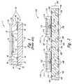
- FIG. 2is a schematic side cross-sectional view of an assembly 100 including a plurality of microelectronic imaging dies 110 (only two are shown) arranged in an array on a support member 160 .
- the individual imaging dies 110include a first side 111 , a second side 113 opposite the first side 111 , and a plurality of ends 115 extending from the first side 111 to the second side 113 .
- the second side 113 of the dies 110is attached to the support member 160 with an adhesive 120 , such as an adhesive film, epoxy, or other suitable material.
- the individual imaging dies 110further include an image sensor 112 on the first side 111 , an integrated circuit 114 (shown schematically) operably coupled to the image sensor 112 , and a plurality of external contacts 116 (e.g., bond-pads) operably coupled to the integrated circuit 114 .
- the image sensors 112can be CMOS devices or CCD image sensors for capturing pictures or other images in the visible spectrum.
- the image sensors 112may also detect radiation in other spectrums (e.g., IR or UV ranges).
- the imaging dies 110 on the support member 160have the same structure. However, in several embodiments, the imaging dies on the support member can have different features to perform different functions.
- the support member 160can be a lead frame or a substrate, such as a printed circuit board, for carrying the imaging dies 110 .
- the support member 160includes a first side 162 having a plurality of terminals 166 and a second side 164 having a plurality of pads 168 .
- the terminals 166can be arranged in arrays for attachment to corresponding external contacts 116 on the dies 110
- the pads 168can be arranged in arrays for attachment to a plurality of conductive couplers (e.g., solder balls).
- the support member 160further includes a plurality of conductive traces 169 electrically coupling the terminals 166 to corresponding pads 168 .
- FIG. 3is a schematic side cross-sectional view of the assembly 100 after wire-bonding the dies 110 to the support member 160 and forming a base 130 between adjacent dies 110 .
- the external contacts 116 of the imaging dies 110are wire-bonded to corresponding terminals 166 on the support member 160 .
- the individual wire-bonds 140include a proximate portion 142 attached to one of the contacts 116 and a distal portion 144 attached to the corresponding terminal 166 .
- the external contacts 116can be electrically connected to terminals on a support member by conductive through-wafer interconnects. Through-wafer interconnects are described in U.S.
- a flowable materialis dispensed onto the support member 160 to form a footing or base 130 for supporting a plurality of covers.
- the flowable materialcan be an epoxy mold compound or another suitable material to at least partially fill the space between adjacent dies 110 .
- the base 130contacts at least a portion of the ends 115 of the individual dies 110 and encapsulates at least the distal portion 144 of the individual wire-bonds 140 .
- the flowable materialcan also be a self-leveling material with a sufficiently low viscosity so that the base 130 has a generally planar support surface 132 to which the covers can be attached.
- a dam(not shown) can be placed around the perimeter of the support member 160 to inhibit material from flowing off the edge of the member 160 and ensure the flowable material has a generally uniform thickness across the member 160 .
- the base 130may not have a generally planar support surface across the support member 160 .
- the volume of flowable material deposited onto the support member 160is selected so that the base 130 has a predetermined height for supporting covers at a precise distance over the image sensors 112 .
- the imaging dies 110project a first distance D 1 from the support member 160
- the base 130projects a second distance D 2 from the support member 160 .
- the first distance D 1is generally equal to the second distance D 2 .
- the first distance D 1can be greater than the second distance D 2 so that the individual imaging dies 110 project above the support surface 132 .
- the second distance D 2can be slightly greater than the first distance D 1 provided that the flow material does not encroach upon the image sensors 112 .
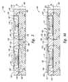
- FIG. 4Ais a schematic side cross-sectional view of the assembly 100 after (a) depositing discrete portions of an adhesive 135 onto the base 130 and/or a plurality of covers 150 and (b) attaching the covers 150 to the base 130 with the covers 150 positioned over corresponding image sensors 112 .
- the adhesive 135can be a tape, a flowable material, or another suitable compound for adhering the covers 150 to the base 130 .
- the adhesive 135can be a UV- or thermally-curable adhesive that is at least partially cured after the covers 150 are attached.
- the adhesive 135has a known thickness D 3 so that the covers 150 are spaced apart from the image sensors 112 by a predetermined and precise distance G, which corresponds to the difference between the first distance D 1 and the sum of the second distance D 2 and the thickness D 3 .
- the covers 150can be glass, quartz, or another suitable material that is transmissive to the desired spectrum of radiation.
- the covers 150for example, can further include one or more anti-reflective films and/or filters.
- FIG. 4Bis a top plan view of a portion of the assembly 100 with the covers 150 removed for clarity.
- the discrete portions of adhesive 135(a) surround corresponding dies 110 and (b) are positioned outboard the proximal portion 142 of the individual wire-bonds 140 and directly over the terminals 166 of the support member 160 ( FIG. 4A ).
- the discrete portions of adhesive 135define a cell 182 ( FIG. 4A ) between the individual dies 110 and corresponding covers 150 .
- the cells 182can be filled with gas, such as air, or an underfill material, as described below with reference to FIG. 7 .
- the discrete portions of adhesivemay not completely surround the individual dies 110 , and/or the discrete portions of adhesive may be placed at a different position relative to the individual dies 110 .
- the adhesivecan be positioned directly over the imaging dies 110 or an interface between the imaging dies 110 and the base 130 .
- FIG. 5is a schematic side cross-sectional view of the assembly 100 after depositing a fill material 180 around the perimeter of the individual covers 150 .
- the fill material 180can be dispensed onto the base 130 via a gap between adjacent covers 150 to encapsulate and cover the ends of the covers 150 and the adhesive 135 .
- the fill material 180(a) increases the robustness of the assembly 100 , (b) enhances the integrity of the joint between the individual covers 150 and the base 130 , and (c) protects the image sensors 112 from moisture, chemicals, and other contaminants.
- the assembly 100may also include a plurality of conductive couplers 190 (shown in broken lines) on corresponding pads 168 of the support member 160 . In several embodiments, however, the assembly 100 may not include the fill material 180 between adjacent covers 150 and/or the conductive couplers 190 .
- the assembly 100can be heated to at least partially cure (i.e., B-stage) the fill material 180 and/or the adhesive 135 .
- the adhesive 135can be cured by heat, exposure to UV light, or another suitable method depending on the type of adhesive.
- the assembly 100can be cut along lines A—A by scribing, sawing, or another suitable process to singulate the individual imaging units 102 .
- One feature of the imaging units 102 illustrated in FIG. 5is that the base 130 provides a support surface 132 with a relatively large area on which to place the adhesive 135 .
- An advantage of this featureis that attaching the adhesive 135 to the relatively large support surface 132 is easier than placing the adhesive 135 on the first side 111 of the die 110 because of the difficulty in positioning the adhesive 135 on the die 110 without covering the image sensor 112 and without damaging the wire-bonds 140 .
- the design of the illustrated imaging units 102reduces the risk of (a) contaminating the image sensor 112 and the external contacts 116 with adhesive material and (b) damaging the wire-bonds 140 while depositing the adhesive 135 .
- the process of manufacturing the illustrated imaging units 102is expected to produce fewer imaging units with defects.
- the illustrated imaging units 102may be manufactured without using expensive and precise alignment equipment to deposit the adhesive 135 and/or attach the covers 150 .
- Another feature of the imaging units 102 illustrated in FIG. 5is that the distal portion 144 of the wire-bonds 140 are encased by the base 130 that supports the covers 150 .
- An advantage of this featureis that the footprint of the individual imaging units 102 is smaller than the footprint of conventional imaging units. The reduced footprint of the imaging units 102 is particularly advantageous for picture cell phones, PDAs, or other applications where space is limited.
- the terminals 18 and the wire-bonds 20are inboard the sidewalls 34 of the chip carrier 30 , which increases the footprint of the imaging unit 1 .
- One feature of the method for manufacturing imaging units 102 illustrated in FIGS. 2–5is that the support member 160 can carry imaging dies 110 with different sizes and/or configurations.
- An advantage of this featureis that the method can be easily adapted to handle various configurations of imaging dies without significant changes to the fabrication process.
- Prior art methodssuch as the method required to form the imaging unit 1 described above with reference to FIG. 1 , may require significant retooling because the chip carriers 30 can only carry imaging dies 10 with a certain shape and size.
- Another advantage of the method for manufacturing imaging units 102 illustrated in FIGS. 2–5is that the method is expected to significantly enhance the efficiency of the manufacturing process because a plurality of imaging units 102 can be fabricated simultaneously using highly accurate and efficient processes developed for packaging and manufacturing semiconductor devices.
- This method of manufacturing imaging units 102is also expected to enhance the quality and performance of the imaging units 102 because the semiconductor fabrication processes can reliably produce and assemble the various components with a high degree of precision.
- several embodiments of the methodare expected to significantly reduce the cost for assembling microelectronic imaging units 102 , increase the performance of the imaging units 102 , and produce higher quality imaging units 102 .
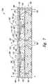
- FIG. 6is a schematic side cross-sectional view of an assembly 200 including a plurality of microelectronic imaging units 202 in accordance with another embodiment of the invention.
- the microelectronic imaging units 202are generally similar to the microelectronic imaging units 102 described above with reference to FIG. 5 .
- the imaging units 202 shown in FIG. 6include a single cover 250 extending over multiple imaging dies 110 that is attached to the base 130 with the adhesive 135 .
- the cover 250can be glass, quartz, or another suitable material that is transmissive to the desired spectrum of radiation. After attaching the cover 250 to the base 130 , the assembly 200 can be cut along lines A—A to singulate the individual imaging units 202 .
- FIG. 7is a schematic side cross-sectional view of an assembly 300 including a plurality of microelectronic imaging units 302 in accordance with another embodiment of the invention.
- the microelectronic imaging units 302are generally similar to the microelectronic imaging units 102 described above with reference to FIG. 5 .
- the imaging units 302 shown in FIG. 7include an underfill 385 disposed across the first side 111 of the imaging dies 110 .
- the underfill 385covers the image sensors 112 and fills the cells 182 between the covers 150 and the imaging dies 110 .
- the underfill 385can be an optical grade material with a high transparency to eliminate or reduce light scattering and/or the loss of images. In applications in which the image sensors 112 have pixels with a smaller size, the underfill 385 can have a higher refractive index to assist in focusing the light for the pixels.
- the underfill 385can be a material that is dimensionally stable over a wide range of temperatures.
- An advantage of this featureis that the distance between the covers 150 and the corresponding image sensors 112 remains generally consistent, even if the imaging units 302 operate in an environment that experiences significant changes in ambient temperature. If the temperature change were to cause the medium between the cover 150 and the image sensor 112 to expand or contract, the associated change in the distance between the cover 150 and the image sensor 112 could skew the images and reduce the life of the imaging unit 302 due to fatigue.
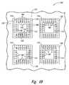
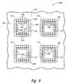
- FIGS. 8–10are schematic top plan views of assemblies having a plurality of microelectronic imaging units in accordance with additional embodiments of the invention.
- the assemblies illustrated in FIGS. 8–10are generally similar to the assembly 100 illustrated in FIG. 4B .
- the assemblies illustrated in FIGS. 8–10include a plurality of imaging dies 110 , a support member (not shown) carrying the dies 110 , a base 130 formed between adjacent dies 110 , and a plurality of covers (not shown for purposes of clarity) over the image sensors 112 .
- the assemblies illustrated in FIGS. 8–10include discrete portions of an adhesive positioned in different arrangements on the dies 110 and/or the base 130 .
- an assembly 400includes discrete portions of an adhesive 435 positioned on the imaging dies 110 and the base 130 over an interface between the individual dies 110 and the base 130 .
- the adhesive 435is positioned inboard the terminals 166 and outboard the external contacts 116 of the imaging dies 110 .
- an assembly 500includes discrete portions of an adhesive 535 positioned on corresponding imaging dies 110 and not on the base 130 . More specifically, the adhesive 535 is disposed inboard the external contacts 116 and outboard the image sensor 112 .
- an assembly 600includes discrete portions of an adhesive 635 arranged in arrays relative to corresponding imaging dies 110 .
- the illustrated arraysinclude four discrete portions of the adhesive 635 on the base 130 positioned proximate to the corners of the individual dies 110 .
- the adhesive 635can have a different number of discrete portions and/or the discrete portions can be arranged differently.
- microelectronic imaging unitscan have any combination of the features described above. Accordingly, the invention is not limited except as by the appended claims.
Landscapes
- Solid State Image Pick-Up Elements (AREA)
Abstract
Description
Claims (32)
Priority Applications (2)
| Application Number | Priority Date | Filing Date | Title |
|---|---|---|---|
| US10/915,180US7364934B2 (en) | 2004-08-10 | 2004-08-10 | Microelectronic imaging units and methods of manufacturing microelectronic imaging units |
| US11/444,404US7498606B2 (en) | 2004-08-10 | 2006-06-01 | Microelectronic imaging units and methods of manufacturing microelectronic imaging units |
Applications Claiming Priority (1)
| Application Number | Priority Date | Filing Date | Title |
|---|---|---|---|
| US10/915,180US7364934B2 (en) | 2004-08-10 | 2004-08-10 | Microelectronic imaging units and methods of manufacturing microelectronic imaging units |
Related Child Applications (1)
| Application Number | Title | Priority Date | Filing Date |
|---|---|---|---|
| US11/444,404DivisionUS7498606B2 (en) | 2004-08-10 | 2006-06-01 | Microelectronic imaging units and methods of manufacturing microelectronic imaging units |
Publications (2)
| Publication Number | Publication Date |
|---|---|
| US20060035402A1 US20060035402A1 (en) | 2006-02-16 |
| US7364934B2true US7364934B2 (en) | 2008-04-29 |
Family
ID=35800478
Family Applications (2)
| Application Number | Title | Priority Date | Filing Date |
|---|---|---|---|
| US10/915,180Expired - LifetimeUS7364934B2 (en) | 2004-08-10 | 2004-08-10 | Microelectronic imaging units and methods of manufacturing microelectronic imaging units |
| US11/444,404Expired - LifetimeUS7498606B2 (en) | 2004-08-10 | 2006-06-01 | Microelectronic imaging units and methods of manufacturing microelectronic imaging units |
Family Applications After (1)
| Application Number | Title | Priority Date | Filing Date |
|---|---|---|---|
| US11/444,404Expired - LifetimeUS7498606B2 (en) | 2004-08-10 | 2006-06-01 | Microelectronic imaging units and methods of manufacturing microelectronic imaging units |
Country Status (1)
| Country | Link |
|---|---|
| US (2) | US7364934B2 (en) |
Cited By (4)
| Publication number | Priority date | Publication date | Assignee | Title |
|---|---|---|---|---|
| US20060035415A1 (en)* | 2004-08-16 | 2006-02-16 | Wood Alan G | Frame structure and semiconductor attach process for use therewith for fabrication of image sensor packages and the like, and resulting packages |
| US20080020511A1 (en)* | 2006-07-19 | 2008-01-24 | Advanced Chip Engineering Technology Inc. | Structure of image sensor module and a method for manufacturing of wafer level package |
| US20080150164A1 (en)* | 2006-12-20 | 2008-06-26 | Phoenix Precision Technology Corporation | Carrier structure embedded with semiconductor chips and method for manufacturing the same |
| US20150163921A1 (en)* | 2013-12-11 | 2015-06-11 | Sasha Oster | Flexible electronic assembly and method |
Families Citing this family (34)
| Publication number | Priority date | Publication date | Assignee | Title |
|---|---|---|---|---|
| US8084866B2 (en) | 2003-12-10 | 2011-12-27 | Micron Technology, Inc. | Microelectronic devices and methods for filling vias in microelectronic devices |
| US7091124B2 (en)* | 2003-11-13 | 2006-08-15 | Micron Technology, Inc. | Methods for forming vias in microelectronic devices, and methods for packaging microelectronic devices |
| US20050247894A1 (en) | 2004-05-05 | 2005-11-10 | Watkins Charles M | Systems and methods for forming apertures in microfeature workpieces |
| US7232754B2 (en)* | 2004-06-29 | 2007-06-19 | Micron Technology, Inc. | Microelectronic devices and methods for forming interconnects in microelectronic devices |
| US7416913B2 (en)* | 2004-07-16 | 2008-08-26 | Micron Technology, Inc. | Methods of manufacturing microelectronic imaging units with discrete standoffs |
| US7189954B2 (en)* | 2004-07-19 | 2007-03-13 | Micron Technology, Inc. | Microelectronic imagers with optical devices and methods of manufacturing such microelectronic imagers |
| US7402453B2 (en)* | 2004-07-28 | 2008-07-22 | Micron Technology, Inc. | Microelectronic imaging units and methods of manufacturing microelectronic imaging units |
| US7364934B2 (en) | 2004-08-10 | 2008-04-29 | Micron Technology, Inc. | Microelectronic imaging units and methods of manufacturing microelectronic imaging units |
| US7425499B2 (en)* | 2004-08-24 | 2008-09-16 | Micron Technology, Inc. | Methods for forming interconnects in vias and microelectronic workpieces including such interconnects |
| US7276393B2 (en)* | 2004-08-26 | 2007-10-02 | Micron Technology, Inc. | Microelectronic imaging units and methods of manufacturing microelectronic imaging units |
| SG120200A1 (en) | 2004-08-27 | 2006-03-28 | Micron Technology Inc | Slanted vias for electrical circuits on circuit boards and other substrates |
| US7300857B2 (en) | 2004-09-02 | 2007-11-27 | Micron Technology, Inc. | Through-wafer interconnects for photoimager and memory wafers |
| US7271482B2 (en)* | 2004-12-30 | 2007-09-18 | Micron Technology, Inc. | Methods for forming interconnects in microelectronic workpieces and microelectronic workpieces formed using such methods |
| US7795134B2 (en) | 2005-06-28 | 2010-09-14 | Micron Technology, Inc. | Conductive interconnect structures and formation methods using supercritical fluids |
| EP1922756B1 (en)* | 2005-08-26 | 2013-05-22 | Philips Intellectual Property & Standards GmbH | Electrically shielded through-wafer interconnect |
| US7622377B2 (en) | 2005-09-01 | 2009-11-24 | Micron Technology, Inc. | Microfeature workpiece substrates having through-substrate vias, and associated methods of formation |
| US7863187B2 (en) | 2005-09-01 | 2011-01-04 | Micron Technology, Inc. | Microfeature workpieces and methods for forming interconnects in microfeature workpieces |
| US7262134B2 (en) | 2005-09-01 | 2007-08-28 | Micron Technology, Inc. | Microfeature workpieces and methods for forming interconnects in microfeature workpieces |
| US7749899B2 (en) | 2006-06-01 | 2010-07-06 | Micron Technology, Inc. | Microelectronic workpieces and methods and systems for forming interconnects in microelectronic workpieces |
| US7629249B2 (en)* | 2006-08-28 | 2009-12-08 | Micron Technology, Inc. | Microfeature workpieces having conductive interconnect structures formed by chemically reactive processes, and associated systems and methods |
| US7902643B2 (en) | 2006-08-31 | 2011-03-08 | Micron Technology, Inc. | Microfeature workpieces having interconnects and conductive backplanes, and associated systems and methods |
| SG149710A1 (en) | 2007-07-12 | 2009-02-27 | Micron Technology Inc | Interconnects for packaged semiconductor devices and methods for manufacturing such devices |
| SG150410A1 (en) | 2007-08-31 | 2009-03-30 | Micron Technology Inc | Partitioned through-layer via and associated systems and methods |
| US7884015B2 (en) | 2007-12-06 | 2011-02-08 | Micron Technology, Inc. | Methods for forming interconnects in microelectronic workpieces and microelectronic workpieces formed using such methods |
| US8084854B2 (en) | 2007-12-28 | 2011-12-27 | Micron Technology, Inc. | Pass-through 3D interconnect for microelectronic dies and associated systems and methods |
| TW200937541A (en)* | 2008-02-20 | 2009-09-01 | Harvatek Corp | Semiconductor chip package structure for achieving electrical connection without using wire-bonding process and manufacturing method thereof |
| TW200939430A (en)* | 2008-03-14 | 2009-09-16 | Harvatek Corp | Semiconductor chip package structure and manufacturing method for achieving front electrical connection without using wire-bonding process |
| CN101562175B (en)* | 2008-04-18 | 2011-11-09 | 鸿富锦精密工业(深圳)有限公司 | Image sensor encapsulating structure and imaging device applied thereof |
| TW200947652A (en)* | 2008-05-12 | 2009-11-16 | Harvatek Corp | Semiconductor chip package structure for achieving positive face electrical connection without using substrates and a wire-bonding process |
| US8253230B2 (en) | 2008-05-15 | 2012-08-28 | Micron Technology, Inc. | Disabling electrical connections using pass-through 3D interconnects and associated systems and methods |
| ITVI20100110A1 (en)* | 2010-04-22 | 2011-10-23 | Fond Bruno Kessler | PHOTOMOLTIPLICATOR DEVICE WITH A PERFECT SOLID STATE |
| JP2016115840A (en)* | 2014-12-16 | 2016-06-23 | ソニー株式会社 | Semiconductor device, solid state image sensor, imaging device, and electronic apparatus |
| KR102720747B1 (en)* | 2015-03-12 | 2024-10-23 | 소니그룹주식회사 | Imaging device, manufacturing method and electronic device |
| CN212211129U (en)* | 2020-04-30 | 2020-12-22 | 华为技术有限公司 | Camera module and electronic equipment |
Citations (140)
| Publication number | Priority date | Publication date | Assignee | Title |
|---|---|---|---|---|
| US3345134A (en) | 1962-04-21 | 1967-10-03 | Knapsack Ag | Process and apparatus for the manufacture of titanium nitride |
| JPS59101882A (en) | 1982-12-03 | 1984-06-12 | Nec Corp | Optical semiconductor device |
| JPS59191388A (en) | 1983-04-14 | 1984-10-30 | Victor Co Of Japan Ltd | semiconductor equipment |
| US4534100A (en) | 1982-06-28 | 1985-08-13 | The United States Of America As Represented By The Secretary Of The Air Force | Electrical method of making conductive paths in silicon |
| US4906314A (en) | 1988-12-30 | 1990-03-06 | Micron Technology, Inc. | Process for simultaneously applying precut swatches of precured polyimide film to each semiconductor die on a wafer |
| WO1990005424A1 (en) | 1988-10-31 | 1990-05-17 | Reimar Lenz | Opto-electronic colour-image sensor |
| US5130783A (en) | 1991-03-04 | 1992-07-14 | Texas Instruments Incorporated | Flexible film semiconductor package |
| US5302778A (en) | 1992-08-28 | 1994-04-12 | Eastman Kodak Company | Semiconductor insulation for optical devices |
| US5371397A (en) | 1992-10-09 | 1994-12-06 | Mitsubishi Denki Kabushiki Kaisha | Solid-state imaging array including focusing elements |
| US5424573A (en) | 1992-03-04 | 1995-06-13 | Hitachi, Ltd. | Semiconductor package having optical interconnection access |
| US5435887A (en) | 1993-11-03 | 1995-07-25 | Massachusetts Institute Of Technology | Methods for the fabrication of microstructure arrays |
| JPH07263607A (en) | 1994-03-17 | 1995-10-13 | Sumitomo Kinzoku Ceramics:Kk | Semiconductor package with j-lead and bending method of lead frame |
| US5505804A (en) | 1993-12-24 | 1996-04-09 | Sharp Kabushiki Kaisha | Method of producing a condenser lens substrate |
| US5593913A (en) | 1993-09-28 | 1997-01-14 | Sharp Kabushiki Kaisha | Method of manufacturing solid state imaging device having high sensitivity and exhibiting high degree of light utilization |
| US5605783A (en) | 1995-01-06 | 1997-02-25 | Eastman Kodak Company | Pattern transfer techniques for fabrication of lenslet arrays for solid state imagers |
| US5672519A (en) | 1994-02-23 | 1997-09-30 | Lg Semicon Co., Ltd. | Method of fabricating solid state image sensing elements |
| US5694246A (en) | 1994-01-03 | 1997-12-02 | Omron Corporation | Method of manufacturing lens array |
| US5708293A (en) | 1996-01-05 | 1998-01-13 | Matsushita Electronics Corporation | Lead frame and method of mounting semiconductor chip |
| US5771158A (en) | 1995-09-21 | 1998-06-23 | Mitsubishi Denki Kabushiki Kaisha | Printed circuit board, printed circuit board used for flat panel display drive circuit, and flat panel display device |
| US5776824A (en) | 1995-12-22 | 1998-07-07 | Micron Technology, Inc. | Method for producing laminated film/metal structures for known good die ("KG") applications |
| US5811799A (en) | 1997-07-31 | 1998-09-22 | Wu; Liang-Chung | Image sensor package having a wall with a sealed cover |
| US5821532A (en) | 1997-06-16 | 1998-10-13 | Eastman Kodak Company | Imager package substrate |
| US5857963A (en) | 1996-07-17 | 1999-01-12 | Welch Allyn, Inc. | Tab imager assembly for use in an endoscope |
| US5861654A (en) | 1995-11-28 | 1999-01-19 | Eastman Kodak Company | Image sensor assembly |
| US5877040A (en) | 1995-08-10 | 1999-03-02 | Lg Semicon Co., Ltd. | Method of making charge-coupled device with microlens |
| US5897338A (en) | 1996-06-11 | 1999-04-27 | European Semiconductor Assembly (Eurasem) B.V. | Method for encapsulating an integrated semi-conductor circuit |
| US5914488A (en) | 1996-03-05 | 1999-06-22 | Mitsubishi Denki Kabushiki Kaisha | Infrared detector |
| US5977535A (en) | 1992-09-30 | 1999-11-02 | Lsi Logic Corporation | Light sensing device having an array of photosensitive elements coincident with an array of lens formed on an optically transmissive material |
| US5998862A (en) | 1993-03-26 | 1999-12-07 | Sony Corporation | Air-packed CCD images package and a mold for manufacturing thereof |
| US6080291A (en) | 1998-07-10 | 2000-06-27 | Semitool, Inc. | Apparatus for electrochemically processing a workpiece including an electrical contact assembly having a seal member |
| US6104086A (en) | 1997-05-20 | 2000-08-15 | Nec Corporation | Semiconductor device having lead terminals bent in J-shape |
| US6114240A (en) | 1997-12-18 | 2000-09-05 | Micron Technology, Inc. | Method for fabricating semiconductor components using focused laser beam |
| US6143588A (en) | 1997-09-09 | 2000-11-07 | Amkor Technology, Inc. | Method of making an integrated circuit package employing a transparent encapsulant |
| JP2001077496A (en) | 1999-09-06 | 2001-03-23 | Ngk Insulators Ltd | Substrate for printed circuit and its manufacture |
| US6236046B1 (en) | 1997-10-28 | 2001-05-22 | Matsushita Electric Works, Ltd. | Infrared sensor |
| US6259083B1 (en) | 1997-08-13 | 2001-07-10 | Sony Corporation | Solid state imaging device and manufacturing method thereof |
| US6266197B1 (en) | 1999-12-08 | 2001-07-24 | Amkor Technology, Inc. | Molded window array for image sensor packages |
| US6274927B1 (en) | 1999-06-03 | 2001-08-14 | Amkor Technology, Inc. | Plastic package for an optical integrated circuit device and method of making |
| US6285064B1 (en) | 2000-03-28 | 2001-09-04 | Omnivision Technologies, Inc. | Chip scale packaging technique for optical image sensing integrated circuits |
| EP1157967A2 (en) | 2000-05-22 | 2001-11-28 | Lucent Technologies Inc. | Packaging micromechanical devices |
| US20020006687A1 (en) | 2000-05-23 | 2002-01-17 | Lam Ken M. | Integrated IC chip package for electronic image sensor die |
| US6351027B1 (en) | 2000-02-29 | 2002-02-26 | Agilent Technologies, Inc. | Chip-mounted enclosure |
| US6368899B1 (en) | 2000-03-08 | 2002-04-09 | Maxwell Electronic Components Group, Inc. | Electronic device packaging |
| US6372548B2 (en) | 1998-06-04 | 2002-04-16 | Matsushita Electric Industrial Co., Ltd. | Method for fabricating a semiconductor package with a semiconductor device attached to a multilayered substrate |
| US6379988B1 (en) | 2000-05-16 | 2002-04-30 | Sandia Corporation | Pre-release plastic packaging of MEMS and IMEMS devices |
| US20020057468A1 (en) | 2000-11-14 | 2002-05-16 | Masao Segawa | Image pickup apparatus, method thereof, and electric apparatus |
| US6407381B1 (en) | 2000-07-05 | 2002-06-18 | Amkor Technology, Inc. | Wafer scale image sensor package |
| US6411439B2 (en) | 1998-05-19 | 2002-06-25 | Seiko Epson Corporation | Microlens array, a manufacturing method therefor, and a display apparatus using the same |
| US20020089025A1 (en) | 2001-01-05 | 2002-07-11 | Li-Kun Chou | Package structure for image IC |
| US20020096729A1 (en) | 2001-01-24 | 2002-07-25 | Tu Hsiu Wen | Stacked package structure of image sensor |
| US20020113296A1 (en) | 2001-02-03 | 2002-08-22 | Samsung Electronics Co., Ltd. | Wafer level hermetic sealing method |
| US6441453B1 (en) | 2001-05-09 | 2002-08-27 | Conexant Systems, Inc. | Clear coating for digital and analog imagers |
| WO2002075815A1 (en) | 2001-03-16 | 2002-09-26 | Atmel Grenoble S.A. | Low cost electronic camera made with integrated circuit technology |
| US20020145676A1 (en) | 2001-02-26 | 2002-10-10 | Tetsuya Kuno | Image pickup apparatus |
| US6483652B2 (en) | 2000-08-17 | 2002-11-19 | Sharp Kabushiki Kaisha | Method for producing solid-state imaging device |
| WO2002095796A2 (en) | 2001-05-18 | 2002-11-28 | Stmicroelectronics Sa | Optical semiconductor housing with incorporated lens and shielding |
| US6503780B1 (en) | 2000-07-05 | 2003-01-07 | Amkor Technology, Inc. | Wafer scale image sensor package fabrication method |
| US6531341B1 (en) | 2000-05-16 | 2003-03-11 | Sandia Corporation | Method of fabricating a microelectronic device package with an integral window |
| US6541762B2 (en) | 2001-08-14 | 2003-04-01 | Samsung Electro-Mechanics Co., Ltd. | Sub chip on board for optical mouse |
| US20030062601A1 (en) | 2001-05-15 | 2003-04-03 | James Harnden | Surface mount package |
| US6560047B2 (en) | 2001-08-29 | 2003-05-06 | Samsung Electro-Mechanics Co., Ltd. | Image module |
| US6566745B1 (en) | 1999-03-29 | 2003-05-20 | Imec Vzw | Image sensor ball grid array package and the fabrication thereof |
| US6603183B1 (en) | 2001-09-04 | 2003-08-05 | Amkor Technology, Inc. | Quick sealing glass-lidded package |
| FR2835654A1 (en) | 2002-02-06 | 2003-08-08 | St Microelectronics Sa | OPTICAL SEMICONDUCTOR PACKAGE WITH COUPLED LENS HOLDER |
| US6617623B2 (en) | 1999-06-15 | 2003-09-09 | Micron Technology, Inc. | Multi-layered gate for a CMOS imager |
| US6661047B2 (en) | 2001-08-30 | 2003-12-09 | Micron Technology, Inc. | CMOS imager and method of formation |
| US6667551B2 (en) | 2000-01-21 | 2003-12-23 | Seiko Epson Corporation | Semiconductor device and manufacturing thereof, including a through-hole with a wider intermediate cavity |
| US6670986B1 (en) | 1998-09-10 | 2003-12-30 | Creo Il. Ltd. | Apparatus for orthogonal movement of a CCD sensor and a method of light sampling therewith |
| US20040012698A1 (en) | 2001-03-05 | 2004-01-22 | Yasuo Suda | Image pickup model and image pickup device |
| US6686588B1 (en) | 2001-01-16 | 2004-02-03 | Amkor Technology, Inc. | Optical module with lens integral holder |
| US20040023469A1 (en) | 2001-03-21 | 2004-02-05 | Canon Kabushiki Kaisha | Semiconductor device and its manufacture method |
| US20040038442A1 (en) | 2002-08-26 | 2004-02-26 | Kinsman Larry D. | Optically interactive device packages and methods of assembly |
| US20040041261A1 (en) | 2002-08-29 | 2004-03-04 | Kinsman Larry D. | Flip-chip image sensor packages and methods of fabrication |
| US6703310B2 (en) | 2001-06-14 | 2004-03-09 | Shinko Electric Industries Co., Ltd. | Semiconductor device and method of production of same |
| US6709898B1 (en) | 2000-10-04 | 2004-03-23 | Intel Corporation | Die-in-heat spreader microelectronic package |
| US20040082094A1 (en) | 2002-10-25 | 2004-04-29 | Katsumi Yamamoto | Method for making and packaging image sensor die using protective coating |
| US6734419B1 (en) | 2001-06-28 | 2004-05-11 | Amkor Technology, Inc. | Method for forming an image sensor package with vision die in lens housing |
| WO2004054001A2 (en) | 2002-12-09 | 2004-06-24 | Quantum Semiconductor Llc | Cmos image sensor |
| US6759266B1 (en) | 2001-09-04 | 2004-07-06 | Amkor Technology, Inc. | Quick sealing glass-lidded package fabrication method |
| US6767753B2 (en)* | 2001-01-17 | 2004-07-27 | Siliconware Precision Industries Co., Ltd. | Image sensor of a quad flat package |
| US6774486B2 (en) | 2001-10-10 | 2004-08-10 | Micron Technology, Inc. | Circuit boards containing vias and methods for producing same |
| US6778046B2 (en) | 2001-09-17 | 2004-08-17 | Magfusion Inc. | Latching micro magnetic relay packages and methods of packaging |
| US6791076B2 (en) | 1999-12-08 | 2004-09-14 | Amkor Technology, Inc. | Image sensor package |
| US20040178495A1 (en) | 2003-03-14 | 2004-09-16 | Yean Tay Wuu | Microelectronic devices and methods for packaging microelectronic devices |
| US6795120B2 (en) | 1996-05-17 | 2004-09-21 | Sony Corporation | Solid-state imaging apparatus and camera using the same |
| US6794223B2 (en) | 2000-09-28 | 2004-09-21 | Intel Corporation | Structure and process for reducing die corner and edge stresses in microelectronic packages |
| US6800943B2 (en) | 2001-04-03 | 2004-10-05 | Matsushita Electric Industrial Co., Ltd. | Solid image pickup device |
| US20040197954A1 (en)* | 2003-04-07 | 2004-10-07 | Walter Moden | Chip scale image sensor semiconductor package and method of fabrication |
| US20040214373A1 (en) | 2003-04-22 | 2004-10-28 | Tongbi Jiang | Packaged microelectronic devices and methods for packaging microelectronic devices |
| US6813154B2 (en) | 2002-12-10 | 2004-11-02 | Motorola, Inc. | Reversible heat sink packaging assembly for an integrated circuit |
| US6825458B1 (en) | 1999-10-30 | 2004-11-30 | Robert Bosch Gmbh | Optoelectronic receiver and method of making an aligned optoelectronic receiver |
| US20040238909A1 (en) | 2003-05-30 | 2004-12-02 | Boon Suan Jeung | Packaged microelectronic devices and methods of packaging microelectronic devices |
| US6828663B2 (en) | 2001-03-07 | 2004-12-07 | Teledyne Technologies Incorporated | Method of packaging a device with a lead frame, and an apparatus formed therefrom |
| US6828674B2 (en) | 2000-04-10 | 2004-12-07 | Analog Devices, Inc. | Hermetically sealed microstructure package |
| US20040245649A1 (en) | 2003-04-16 | 2004-12-09 | Seiko Epson Corporation | Optical device, optical module, semiconductor apparatus and its manufacturing method, and electronic apparatus |
| US20050004560A1 (en) | 2001-06-20 | 2005-01-06 | Microvention, Inc. | Medical devices having full or partial polymer coatings and their methods of manufacture |
| US6844978B2 (en) | 1997-10-03 | 2005-01-18 | Digital Optics Corp. | Wafer level creation of multiple optical elements |
| US6864172B2 (en) | 2002-06-18 | 2005-03-08 | Sanyo Electric Co., Ltd. | Manufacturing method of semiconductor device |
| US20050052751A1 (en) | 2000-12-27 | 2005-03-10 | Yue Liu | Wafer integration of micro-optics |
| US20050063033A1 (en) | 2003-09-18 | 2005-03-24 | Kinsman Larry D. | Microelectronic devices and methods for packaging microelectronic devices |
| US20050104228A1 (en) | 2003-11-13 | 2005-05-19 | Rigg Sidney B. | Microelectronic devices, methods for forming vias in microelectronic devices, and methods for packaging microelectronic devices |
| US20050110889A1 (en) | 2003-11-26 | 2005-05-26 | Tuttle Mark E. | Packaged microelectronic imagers and methods of packaging microelectronic imagers |
| US20050127478A1 (en) | 2003-12-10 | 2005-06-16 | Hiatt William M. | Microelectronic devices and methods for filling vias in microelectronic devices |
| US20050151228A1 (en) | 2003-12-04 | 2005-07-14 | Kazumasa Tanida | Semiconductor chip and manufacturing method for the same, and semiconductor device |
| US20050151272A1 (en) | 2004-01-06 | 2005-07-14 | Street Bret K. | Die package having an adhesive flow restriction area |
| US20050184219A1 (en) | 2004-02-23 | 2005-08-25 | Kirby Kyle K. | Packaged microelectronic imagers and methods of packaging microelectronic imagers |
| US20050236708A1 (en) | 2004-04-27 | 2005-10-27 | Farnworth Warren M | Microelectronic imaging devices and methods of packaging microelectronic imaging devices |
| US20050253213A1 (en)* | 2004-05-13 | 2005-11-17 | Tongbi Jiang | Covers for microelectronic imagers and methods for wafer-level packaging of microelectronics imagers |
| US20050254133A1 (en) | 2004-05-13 | 2005-11-17 | Salman Akram | Integrated optics units and methods of manufacturing integrated optics units for use with microelectronic imagers |
| US20050270651A1 (en) | 2004-06-02 | 2005-12-08 | Boettiger Ulrich C | Apparatus and method for manufacturing positive or negative microlenses |
| US20050275049A1 (en) | 2004-06-10 | 2005-12-15 | Kirby Kyle K | Packaged microelectronic imagers and methods of packging microelectronic imagers |
| US20050275750A1 (en) | 2004-06-09 | 2005-12-15 | Salman Akram | Wafer-level packaged microelectronic imagers and processes for wafer-level packaging |
| US20050275048A1 (en) | 2004-06-14 | 2005-12-15 | Farnworth Warren M | Microelectronic imagers and methods of packaging microelectronic imagers |
| US20050287783A1 (en) | 2004-06-29 | 2005-12-29 | Kirby Kyle K | Microelectronic devices and methods for forming interconnects in microelectronic devices |
| US20050285154A1 (en) | 2004-06-29 | 2005-12-29 | Salman Akram | Packaged microelectronic imagers and methods of packaging microelectronic imagers |
| US20060014313A1 (en) | 2004-07-16 | 2006-01-19 | Hall Frank L | Microelectronic imaging units and methods of manufacturing microelectronic imaging units |
| US20060023107A1 (en) | 2004-08-02 | 2006-02-02 | Bolken Todd O | Microelectronic imagers with optics supports having threadless interfaces and methods for manufacturing such microelectronic imagers |
| US20060024856A1 (en) | 2004-07-28 | 2006-02-02 | Derderian James M | Microelectronic imaging units and methods of manufacturing microelectronic imaging units |
| US20060035401A1 (en) | 2004-08-12 | 2006-02-16 | Fuji Photo Film Co., Ltd. | Solid state image pickup device capable of suppressing smear |
| US20060035415A1 (en) | 2004-08-16 | 2006-02-16 | Wood Alan G | Frame structure and semiconductor attach process for use therewith for fabrication of image sensor packages and the like, and resulting packages |
| US20060035402A1 (en) | 2004-08-10 | 2006-02-16 | Street Bret K | Microelectronic imaging units and methods of manufacturing microelectronic imaging units |
| US20060040421A1 (en) | 2004-08-19 | 2006-02-23 | Farnworth Warren M | Spacers for packaged microelectronic imagers and methods of making and using spacers for wafer-level packaging of imagers |
| US20060038183A1 (en) | 2004-08-19 | 2006-02-23 | Oliver Steven D | Microelectronic imagers with curved image sensors and methods for manufacturing microelectronic imagers |
| US20060046471A1 (en) | 2004-08-27 | 2006-03-02 | Kirby Kyle K | Methods for forming vias of varying lateral dimensions and semiconductor components and assemblies including same |
| US20060043509A1 (en) | 2004-08-24 | 2006-03-02 | Watkins Charles M | Packaged microelectronic imaging devices and methods of packaging microelectronic imaging devices |
| US20060042952A1 (en) | 2004-08-24 | 2006-03-02 | Oliver Steven D | Methods for forming interconnects in vias and microelectronic workpieces including such interconnects |
| US20060044433A1 (en) | 2004-08-31 | 2006-03-02 | Micron Technology, Inc. | Microelectronic imagers having front side contacts and methods of packaging such microelectronic imagers |
| US20060043599A1 (en) | 2004-09-02 | 2006-03-02 | Salman Akram | Through-wafer interconnects for photoimager and memory wafers |
| US20060046332A1 (en) | 2004-08-26 | 2006-03-02 | Derderian James M | Microelectronic Imaging units and methods of manufacturing microelectronic imaging units |
| US20060043512A1 (en) | 2004-08-24 | 2006-03-02 | Oliver Steven D | Microelectronic imagers with optical devices having integral reference features and methods for manufacturing such microelectronic imagers |
| US20060043262A1 (en) | 2004-08-30 | 2006-03-02 | Micron Technology, Inc. | Microelectronic imagers with integrated optical devices and methods for manufacturing such microelectronic imagers |
| US20060046537A1 (en) | 2004-08-27 | 2006-03-02 | Chong Chin H | Slanted vias for electrical circuits on circuit boards and other substrates |
| US20060148250A1 (en) | 2004-12-30 | 2006-07-06 | Micron Technology, Inc. | Methods for forming interconnects in microelectronic workpieces and microelectronic workpieces formed using such methods |
| US20060177999A1 (en) | 2005-02-10 | 2006-08-10 | Micron Technology, Inc. | Microelectronic workpieces and methods for forming interconnects in microelectronic workpieces |
| US20060175532A1 (en) | 2005-02-08 | 2006-08-10 | Micron Technology, Inc. | Microelectronic imaging units and methods of manufacturing microelectronic imaging units |
| US20060177959A1 (en) | 2005-02-10 | 2006-08-10 | Micron Technology, Inc. | Microfeature workpieces having microlenses and methods of forming microlenses on microfeature workpieces |
| US7091571B1 (en)* | 2003-12-11 | 2006-08-15 | Amkor Technology, Inc. | Image sensor package and method for manufacture thereof |
| US20060186492A1 (en) | 2005-02-18 | 2006-08-24 | Micron Technology, Inc. | Microelectronic imagers with shaped image sensors and methods for manufacturing microelectronic imagers |
| US20060289968A1 (en) | 2005-06-28 | 2006-12-28 | Micron Technology, Inc. | Conductive interconnect structures and formation methods using supercritical fluids |
| US20060290001A1 (en) | 2005-06-28 | 2006-12-28 | Micron Technology, Inc. | Interconnect vias and associated methods of formation |
Family Cites Families (2)
| Publication number | Priority date | Publication date | Assignee | Title |
|---|---|---|---|---|
| US5916625A (en)* | 1993-04-08 | 1999-06-29 | Ppg Industries, Inc. | Method and apparatus for spraying waterborne coatings under varying conditions |
| JP2872051B2 (en)* | 1994-10-04 | 1999-03-17 | カーネル技研株式会社 | Underwater glasses |
- 2004
- 2004-08-10USUS10/915,180patent/US7364934B2/ennot_activeExpired - Lifetime
- 2006
- 2006-06-01USUS11/444,404patent/US7498606B2/ennot_activeExpired - Lifetime
Patent Citations (152)
| Publication number | Priority date | Publication date | Assignee | Title |
|---|---|---|---|---|
| US3345134A (en) | 1962-04-21 | 1967-10-03 | Knapsack Ag | Process and apparatus for the manufacture of titanium nitride |
| US4534100A (en) | 1982-06-28 | 1985-08-13 | The United States Of America As Represented By The Secretary Of The Air Force | Electrical method of making conductive paths in silicon |
| JPS59101882A (en) | 1982-12-03 | 1984-06-12 | Nec Corp | Optical semiconductor device |
| JPS59191388A (en) | 1983-04-14 | 1984-10-30 | Victor Co Of Japan Ltd | semiconductor equipment |
| WO1990005424A1 (en) | 1988-10-31 | 1990-05-17 | Reimar Lenz | Opto-electronic colour-image sensor |
| US4906314A (en) | 1988-12-30 | 1990-03-06 | Micron Technology, Inc. | Process for simultaneously applying precut swatches of precured polyimide film to each semiconductor die on a wafer |
| US5130783A (en) | 1991-03-04 | 1992-07-14 | Texas Instruments Incorporated | Flexible film semiconductor package |
| US5424573A (en) | 1992-03-04 | 1995-06-13 | Hitachi, Ltd. | Semiconductor package having optical interconnection access |
| US5302778A (en) | 1992-08-28 | 1994-04-12 | Eastman Kodak Company | Semiconductor insulation for optical devices |
| US5977535A (en) | 1992-09-30 | 1999-11-02 | Lsi Logic Corporation | Light sensing device having an array of photosensitive elements coincident with an array of lens formed on an optically transmissive material |
| US5371397A (en) | 1992-10-09 | 1994-12-06 | Mitsubishi Denki Kabushiki Kaisha | Solid-state imaging array including focusing elements |
| US5998862A (en) | 1993-03-26 | 1999-12-07 | Sony Corporation | Air-packed CCD images package and a mold for manufacturing thereof |
| US5593913A (en) | 1993-09-28 | 1997-01-14 | Sharp Kabushiki Kaisha | Method of manufacturing solid state imaging device having high sensitivity and exhibiting high degree of light utilization |
| US5435887A (en) | 1993-11-03 | 1995-07-25 | Massachusetts Institute Of Technology | Methods for the fabrication of microstructure arrays |
| US5505804A (en) | 1993-12-24 | 1996-04-09 | Sharp Kabushiki Kaisha | Method of producing a condenser lens substrate |
| US5694246A (en) | 1994-01-03 | 1997-12-02 | Omron Corporation | Method of manufacturing lens array |
| US5672519A (en) | 1994-02-23 | 1997-09-30 | Lg Semicon Co., Ltd. | Method of fabricating solid state image sensing elements |
| JPH07263607A (en) | 1994-03-17 | 1995-10-13 | Sumitomo Kinzoku Ceramics:Kk | Semiconductor package with j-lead and bending method of lead frame |
| US5605783A (en) | 1995-01-06 | 1997-02-25 | Eastman Kodak Company | Pattern transfer techniques for fabrication of lenslet arrays for solid state imagers |
| US5877040A (en) | 1995-08-10 | 1999-03-02 | Lg Semicon Co., Ltd. | Method of making charge-coupled device with microlens |
| US5771158A (en) | 1995-09-21 | 1998-06-23 | Mitsubishi Denki Kabushiki Kaisha | Printed circuit board, printed circuit board used for flat panel display drive circuit, and flat panel display device |
| US5861654A (en) | 1995-11-28 | 1999-01-19 | Eastman Kodak Company | Image sensor assembly |
| US5776824A (en) | 1995-12-22 | 1998-07-07 | Micron Technology, Inc. | Method for producing laminated film/metal structures for known good die ("KG") applications |
| US5708293A (en) | 1996-01-05 | 1998-01-13 | Matsushita Electronics Corporation | Lead frame and method of mounting semiconductor chip |
| US5914488A (en) | 1996-03-05 | 1999-06-22 | Mitsubishi Denki Kabushiki Kaisha | Infrared detector |
| US6795120B2 (en) | 1996-05-17 | 2004-09-21 | Sony Corporation | Solid-state imaging apparatus and camera using the same |
| US5897338A (en) | 1996-06-11 | 1999-04-27 | European Semiconductor Assembly (Eurasem) B.V. | Method for encapsulating an integrated semi-conductor circuit |
| US5857963A (en) | 1996-07-17 | 1999-01-12 | Welch Allyn, Inc. | Tab imager assembly for use in an endoscope |
| US6104086A (en) | 1997-05-20 | 2000-08-15 | Nec Corporation | Semiconductor device having lead terminals bent in J-shape |
| EP0886323A2 (en) | 1997-06-16 | 1998-12-23 | Eastman Kodak Company | Imager package substrate |
| US5821532A (en) | 1997-06-16 | 1998-10-13 | Eastman Kodak Company | Imager package substrate |
| US5811799A (en) | 1997-07-31 | 1998-09-22 | Wu; Liang-Chung | Image sensor package having a wall with a sealed cover |
| US6259083B1 (en) | 1997-08-13 | 2001-07-10 | Sony Corporation | Solid state imaging device and manufacturing method thereof |
| US6143588A (en) | 1997-09-09 | 2000-11-07 | Amkor Technology, Inc. | Method of making an integrated circuit package employing a transparent encapsulant |
| US6844978B2 (en) | 1997-10-03 | 2005-01-18 | Digital Optics Corp. | Wafer level creation of multiple optical elements |
| US6236046B1 (en) | 1997-10-28 | 2001-05-22 | Matsushita Electric Works, Ltd. | Infrared sensor |
| US6114240A (en) | 1997-12-18 | 2000-09-05 | Micron Technology, Inc. | Method for fabricating semiconductor components using focused laser beam |
| US6411439B2 (en) | 1998-05-19 | 2002-06-25 | Seiko Epson Corporation | Microlens array, a manufacturing method therefor, and a display apparatus using the same |
| US6372548B2 (en) | 1998-06-04 | 2002-04-16 | Matsushita Electric Industrial Co., Ltd. | Method for fabricating a semiconductor package with a semiconductor device attached to a multilayered substrate |
| US6080291A (en) | 1998-07-10 | 2000-06-27 | Semitool, Inc. | Apparatus for electrochemically processing a workpiece including an electrical contact assembly having a seal member |
| US6670986B1 (en) | 1998-09-10 | 2003-12-30 | Creo Il. Ltd. | Apparatus for orthogonal movement of a CCD sensor and a method of light sampling therewith |
| US6566745B1 (en) | 1999-03-29 | 2003-05-20 | Imec Vzw | Image sensor ball grid array package and the fabrication thereof |
| US6420204B2 (en) | 1999-06-03 | 2002-07-16 | Amkor Technology, Inc. | Method of making a plastic package for an optical integrated circuit device |
| US6274927B1 (en) | 1999-06-03 | 2001-08-14 | Amkor Technology, Inc. | Plastic package for an optical integrated circuit device and method of making |
| US6617623B2 (en) | 1999-06-15 | 2003-09-09 | Micron Technology, Inc. | Multi-layered gate for a CMOS imager |
| JP2001077496A (en) | 1999-09-06 | 2001-03-23 | Ngk Insulators Ltd | Substrate for printed circuit and its manufacture |
| US6825458B1 (en) | 1999-10-30 | 2004-11-30 | Robert Bosch Gmbh | Optoelectronic receiver and method of making an aligned optoelectronic receiver |
| US6266197B1 (en) | 1999-12-08 | 2001-07-24 | Amkor Technology, Inc. | Molded window array for image sensor packages |
| US6791076B2 (en) | 1999-12-08 | 2004-09-14 | Amkor Technology, Inc. | Image sensor package |
| US6667551B2 (en) | 2000-01-21 | 2003-12-23 | Seiko Epson Corporation | Semiconductor device and manufacturing thereof, including a through-hole with a wider intermediate cavity |
| US6351027B1 (en) | 2000-02-29 | 2002-02-26 | Agilent Technologies, Inc. | Chip-mounted enclosure |
| US6368899B1 (en) | 2000-03-08 | 2002-04-09 | Maxwell Electronic Components Group, Inc. | Electronic device packaging |
| US6285064B1 (en) | 2000-03-28 | 2001-09-04 | Omnivision Technologies, Inc. | Chip scale packaging technique for optical image sensing integrated circuits |
| US6828674B2 (en) | 2000-04-10 | 2004-12-07 | Analog Devices, Inc. | Hermetically sealed microstructure package |
| US6531341B1 (en) | 2000-05-16 | 2003-03-11 | Sandia Corporation | Method of fabricating a microelectronic device package with an integral window |
| US6379988B1 (en) | 2000-05-16 | 2002-04-30 | Sandia Corporation | Pre-release plastic packaging of MEMS and IMEMS devices |
| EP1157967A2 (en) | 2000-05-22 | 2001-11-28 | Lucent Technologies Inc. | Packaging micromechanical devices |
| US20020006687A1 (en) | 2000-05-23 | 2002-01-17 | Lam Ken M. | Integrated IC chip package for electronic image sensor die |
| US6503780B1 (en) | 2000-07-05 | 2003-01-07 | Amkor Technology, Inc. | Wafer scale image sensor package fabrication method |
| US6407381B1 (en) | 2000-07-05 | 2002-06-18 | Amkor Technology, Inc. | Wafer scale image sensor package |
| US6483652B2 (en) | 2000-08-17 | 2002-11-19 | Sharp Kabushiki Kaisha | Method for producing solid-state imaging device |
| US6794223B2 (en) | 2000-09-28 | 2004-09-21 | Intel Corporation | Structure and process for reducing die corner and edge stresses in microelectronic packages |
| US6709898B1 (en) | 2000-10-04 | 2004-03-23 | Intel Corporation | Die-in-heat spreader microelectronic package |
| US20020057468A1 (en) | 2000-11-14 | 2002-05-16 | Masao Segawa | Image pickup apparatus, method thereof, and electric apparatus |
| US20050052751A1 (en) | 2000-12-27 | 2005-03-10 | Yue Liu | Wafer integration of micro-optics |
| US20020089025A1 (en) | 2001-01-05 | 2002-07-11 | Li-Kun Chou | Package structure for image IC |
| US6686588B1 (en) | 2001-01-16 | 2004-02-03 | Amkor Technology, Inc. | Optical module with lens integral holder |
| US6767753B2 (en)* | 2001-01-17 | 2004-07-27 | Siliconware Precision Industries Co., Ltd. | Image sensor of a quad flat package |
| US20020096729A1 (en) | 2001-01-24 | 2002-07-25 | Tu Hsiu Wen | Stacked package structure of image sensor |
| US20020113296A1 (en) | 2001-02-03 | 2002-08-22 | Samsung Electronics Co., Ltd. | Wafer level hermetic sealing method |
| US20020145676A1 (en) | 2001-02-26 | 2002-10-10 | Tetsuya Kuno | Image pickup apparatus |
| US20040012698A1 (en) | 2001-03-05 | 2004-01-22 | Yasuo Suda | Image pickup model and image pickup device |
| US6828663B2 (en) | 2001-03-07 | 2004-12-07 | Teledyne Technologies Incorporated | Method of packaging a device with a lead frame, and an apparatus formed therefrom |
| WO2002075815A1 (en) | 2001-03-16 | 2002-09-26 | Atmel Grenoble S.A. | Low cost electronic camera made with integrated circuit technology |
| US20040023469A1 (en) | 2001-03-21 | 2004-02-05 | Canon Kabushiki Kaisha | Semiconductor device and its manufacture method |
| US6800943B2 (en) | 2001-04-03 | 2004-10-05 | Matsushita Electric Industrial Co., Ltd. | Solid image pickup device |
| US6441453B1 (en) | 2001-05-09 | 2002-08-27 | Conexant Systems, Inc. | Clear coating for digital and analog imagers |
| US20030062601A1 (en) | 2001-05-15 | 2003-04-03 | James Harnden | Surface mount package |
| WO2002095796A2 (en) | 2001-05-18 | 2002-11-28 | Stmicroelectronics Sa | Optical semiconductor housing with incorporated lens and shielding |
| US6703310B2 (en) | 2001-06-14 | 2004-03-09 | Shinko Electric Industries Co., Ltd. | Semiconductor device and method of production of same |
| US20050004560A1 (en) | 2001-06-20 | 2005-01-06 | Microvention, Inc. | Medical devices having full or partial polymer coatings and their methods of manufacture |
| US6734419B1 (en) | 2001-06-28 | 2004-05-11 | Amkor Technology, Inc. | Method for forming an image sensor package with vision die in lens housing |
| US6541762B2 (en) | 2001-08-14 | 2003-04-01 | Samsung Electro-Mechanics Co., Ltd. | Sub chip on board for optical mouse |
| US6560047B2 (en) | 2001-08-29 | 2003-05-06 | Samsung Electro-Mechanics Co., Ltd. | Image module |
| US6661047B2 (en) | 2001-08-30 | 2003-12-09 | Micron Technology, Inc. | CMOS imager and method of formation |
| US6759266B1 (en) | 2001-09-04 | 2004-07-06 | Amkor Technology, Inc. | Quick sealing glass-lidded package fabrication method |
| US6603183B1 (en) | 2001-09-04 | 2003-08-05 | Amkor Technology, Inc. | Quick sealing glass-lidded package |
| US6778046B2 (en) | 2001-09-17 | 2004-08-17 | Magfusion Inc. | Latching micro magnetic relay packages and methods of packaging |
| US6774486B2 (en) | 2001-10-10 | 2004-08-10 | Micron Technology, Inc. | Circuit boards containing vias and methods for producing same |
| US6797616B2 (en) | 2001-10-10 | 2004-09-28 | Micron Technology, Inc. | Circuit boards containing vias and methods for producing same |
| FR2835654A1 (en) | 2002-02-06 | 2003-08-08 | St Microelectronics Sa | OPTICAL SEMICONDUCTOR PACKAGE WITH COUPLED LENS HOLDER |
| US6864172B2 (en) | 2002-06-18 | 2005-03-08 | Sanyo Electric Co., Ltd. | Manufacturing method of semiconductor device |
| US20040038442A1 (en) | 2002-08-26 | 2004-02-26 | Kinsman Larry D. | Optically interactive device packages and methods of assembly |
| US20040041261A1 (en) | 2002-08-29 | 2004-03-04 | Kinsman Larry D. | Flip-chip image sensor packages and methods of fabrication |
| US7122390B2 (en) | 2002-08-29 | 2006-10-17 | Micron Technology, Inc. | Methods of fabrication for flip-chip image sensor packages |
| US6885107B2 (en) | 2002-08-29 | 2005-04-26 | Micron Technology, Inc. | Flip-chip image sensor packages and methods of fabrication |
| US20040082094A1 (en) | 2002-10-25 | 2004-04-29 | Katsumi Yamamoto | Method for making and packaging image sensor die using protective coating |
| WO2004054001A2 (en) | 2002-12-09 | 2004-06-24 | Quantum Semiconductor Llc | Cmos image sensor |
| US6813154B2 (en) | 2002-12-10 | 2004-11-02 | Motorola, Inc. | Reversible heat sink packaging assembly for an integrated circuit |
| US20040178495A1 (en) | 2003-03-14 | 2004-09-16 | Yean Tay Wuu | Microelectronic devices and methods for packaging microelectronic devices |
| US6946325B2 (en) | 2003-03-14 | 2005-09-20 | Micron Technology, Inc. | Methods for packaging microelectronic devices |
| US20040197954A1 (en)* | 2003-04-07 | 2004-10-07 | Walter Moden | Chip scale image sensor semiconductor package and method of fabrication |
| US20040245649A1 (en) | 2003-04-16 | 2004-12-09 | Seiko Epson Corporation | Optical device, optical module, semiconductor apparatus and its manufacturing method, and electronic apparatus |
| US20040214373A1 (en) | 2003-04-22 | 2004-10-28 | Tongbi Jiang | Packaged microelectronic devices and methods for packaging microelectronic devices |
| US6882021B2 (en) | 2003-05-30 | 2005-04-19 | Micron Technology, Inc. | Packaged image sensing microelectronic devices including a lead and methods of packaging image sensing microelectronic devices including a lead |
| US20040238909A1 (en) | 2003-05-30 | 2004-12-02 | Boon Suan Jeung | Packaged microelectronic devices and methods of packaging microelectronic devices |
| US20050255628A1 (en) | 2003-09-18 | 2005-11-17 | Micron Technology, Inc. | Microelectronic devices and methods for packaging microelectronic devices |
| US6934065B2 (en)* | 2003-09-18 | 2005-08-23 | Micron Technology, Inc. | Microelectronic devices and methods for packaging microelectronic devices |
| US20050063033A1 (en) | 2003-09-18 | 2005-03-24 | Kinsman Larry D. | Microelectronic devices and methods for packaging microelectronic devices |
| US20050104228A1 (en) | 2003-11-13 | 2005-05-19 | Rigg Sidney B. | Microelectronic devices, methods for forming vias in microelectronic devices, and methods for packaging microelectronic devices |
| US20050231626A1 (en) | 2003-11-26 | 2005-10-20 | Micron Technology, Inc. | Packaged microelectronic imagers and methods of packaging microelectronic imagers |
| US20050110889A1 (en) | 2003-11-26 | 2005-05-26 | Tuttle Mark E. | Packaged microelectronic imagers and methods of packaging microelectronic imagers |
| US20050151228A1 (en) | 2003-12-04 | 2005-07-14 | Kazumasa Tanida | Semiconductor chip and manufacturing method for the same, and semiconductor device |
| US20050127478A1 (en) | 2003-12-10 | 2005-06-16 | Hiatt William M. | Microelectronic devices and methods for filling vias in microelectronic devices |
| US7091571B1 (en)* | 2003-12-11 | 2006-08-15 | Amkor Technology, Inc. | Image sensor package and method for manufacture thereof |
| US20050151272A1 (en) | 2004-01-06 | 2005-07-14 | Street Bret K. | Die package having an adhesive flow restriction area |
| US20050184219A1 (en) | 2004-02-23 | 2005-08-25 | Kirby Kyle K. | Packaged microelectronic imagers and methods of packaging microelectronic imagers |
| US20050236708A1 (en) | 2004-04-27 | 2005-10-27 | Farnworth Warren M | Microelectronic imaging devices and methods of packaging microelectronic imaging devices |
| US20050253213A1 (en)* | 2004-05-13 | 2005-11-17 | Tongbi Jiang | Covers for microelectronic imagers and methods for wafer-level packaging of microelectronics imagers |
| US20050254133A1 (en) | 2004-05-13 | 2005-11-17 | Salman Akram | Integrated optics units and methods of manufacturing integrated optics units for use with microelectronic imagers |
| US20050270651A1 (en) | 2004-06-02 | 2005-12-08 | Boettiger Ulrich C | Apparatus and method for manufacturing positive or negative microlenses |
| US20050275750A1 (en) | 2004-06-09 | 2005-12-15 | Salman Akram | Wafer-level packaged microelectronic imagers and processes for wafer-level packaging |
| US20050275049A1 (en) | 2004-06-10 | 2005-12-15 | Kirby Kyle K | Packaged microelectronic imagers and methods of packging microelectronic imagers |
| US20050275048A1 (en) | 2004-06-14 | 2005-12-15 | Farnworth Warren M | Microelectronic imagers and methods of packaging microelectronic imagers |
| US20050287783A1 (en) | 2004-06-29 | 2005-12-29 | Kirby Kyle K | Microelectronic devices and methods for forming interconnects in microelectronic devices |
| US20050285154A1 (en) | 2004-06-29 | 2005-12-29 | Salman Akram | Packaged microelectronic imagers and methods of packaging microelectronic imagers |
| US20060014313A1 (en) | 2004-07-16 | 2006-01-19 | Hall Frank L | Microelectronic imaging units and methods of manufacturing microelectronic imaging units |
| US20060024856A1 (en) | 2004-07-28 | 2006-02-02 | Derderian James M | Microelectronic imaging units and methods of manufacturing microelectronic imaging units |
| US20060023107A1 (en) | 2004-08-02 | 2006-02-02 | Bolken Todd O | Microelectronic imagers with optics supports having threadless interfaces and methods for manufacturing such microelectronic imagers |
| US20060035402A1 (en) | 2004-08-10 | 2006-02-16 | Street Bret K | Microelectronic imaging units and methods of manufacturing microelectronic imaging units |
| US20060216850A1 (en) | 2004-08-10 | 2006-09-28 | Street Bret K | Microelectronic imaging units and methods of manufacturing microelectronic imaging units |
| US20060035401A1 (en) | 2004-08-12 | 2006-02-16 | Fuji Photo Film Co., Ltd. | Solid state image pickup device capable of suppressing smear |
| US20060035415A1 (en) | 2004-08-16 | 2006-02-16 | Wood Alan G | Frame structure and semiconductor attach process for use therewith for fabrication of image sensor packages and the like, and resulting packages |
| US20060038183A1 (en) | 2004-08-19 | 2006-02-23 | Oliver Steven D | Microelectronic imagers with curved image sensors and methods for manufacturing microelectronic imagers |
| US20060040421A1 (en) | 2004-08-19 | 2006-02-23 | Farnworth Warren M | Spacers for packaged microelectronic imagers and methods of making and using spacers for wafer-level packaging of imagers |
| US20060042952A1 (en) | 2004-08-24 | 2006-03-02 | Oliver Steven D | Methods for forming interconnects in vias and microelectronic workpieces including such interconnects |
| US20060043509A1 (en) | 2004-08-24 | 2006-03-02 | Watkins Charles M | Packaged microelectronic imaging devices and methods of packaging microelectronic imaging devices |
| US20060043512A1 (en) | 2004-08-24 | 2006-03-02 | Oliver Steven D | Microelectronic imagers with optical devices having integral reference features and methods for manufacturing such microelectronic imagers |
| US20060046332A1 (en) | 2004-08-26 | 2006-03-02 | Derderian James M | Microelectronic Imaging units and methods of manufacturing microelectronic imaging units |
| US20060223207A1 (en) | 2004-08-26 | 2006-10-05 | Derderian James M | Microelectronic imaging units and methods of manufacturing microelectronic imaging units |
| US20060046471A1 (en) | 2004-08-27 | 2006-03-02 | Kirby Kyle K | Methods for forming vias of varying lateral dimensions and semiconductor components and assemblies including same |
| US20060046537A1 (en) | 2004-08-27 | 2006-03-02 | Chong Chin H | Slanted vias for electrical circuits on circuit boards and other substrates |
| US20060043262A1 (en) | 2004-08-30 | 2006-03-02 | Micron Technology, Inc. | Microelectronic imagers with integrated optical devices and methods for manufacturing such microelectronic imagers |
| US20060044433A1 (en) | 2004-08-31 | 2006-03-02 | Micron Technology, Inc. | Microelectronic imagers having front side contacts and methods of packaging such microelectronic imagers |
| US20060043599A1 (en) | 2004-09-02 | 2006-03-02 | Salman Akram | Through-wafer interconnects for photoimager and memory wafers |
| US20060148250A1 (en) | 2004-12-30 | 2006-07-06 | Micron Technology, Inc. | Methods for forming interconnects in microelectronic workpieces and microelectronic workpieces formed using such methods |
| US20060175532A1 (en) | 2005-02-08 | 2006-08-10 | Micron Technology, Inc. | Microelectronic imaging units and methods of manufacturing microelectronic imaging units |
| US20060177959A1 (en) | 2005-02-10 | 2006-08-10 | Micron Technology, Inc. | Microfeature workpieces having microlenses and methods of forming microlenses on microfeature workpieces |
| US20060177999A1 (en) | 2005-02-10 | 2006-08-10 | Micron Technology, Inc. | Microelectronic workpieces and methods for forming interconnects in microelectronic workpieces |
| US20060186492A1 (en) | 2005-02-18 | 2006-08-24 | Micron Technology, Inc. | Microelectronic imagers with shaped image sensors and methods for manufacturing microelectronic imagers |
| US20060289968A1 (en) | 2005-06-28 | 2006-12-28 | Micron Technology, Inc. | Conductive interconnect structures and formation methods using supercritical fluids |
| US20060290001A1 (en) | 2005-06-28 | 2006-12-28 | Micron Technology, Inc. | Interconnect vias and associated methods of formation |
Non-Patent Citations (77)
| Title |
|---|
| Aachboun, S. and P. Ranson, "Cryogenic etching of deep narrow trenches in silicon," J. Vac. Sci. Technol. A 18(4), Jul./Aug. 2000, pp. 1848-1852. |
| Aachboun, S. and P. Ranson, "Deep anisotropic etching of silicon," J. Vac. Sci. Technol. A 17(4), Jul./Aug. 1999, pp. 2270-2273. |
| Austin, M.D. and S.Y. Chou, "Fabrication of 70 nm channel length polymer organic thin-film transistors using nanoimprint lithography," Applied Physics Letters, vol. 81, No. 23, pp. 4431-4433, Dec. 2, 2002, American Institute of Physics. |
| Blackburn, J.M. et al., "Deposition of Conformal Copper and Nickel Films from Supercritical Carbon Dioxide," Science, vol. 294, pp. 141-145, Oct. 5, 2001. |
| Brubaker, C. et al., "Ultra-thick Lithography for Advanced Packaging and MEMS," SPIE's 27th Annual International Symposium on Microlithography 2002, Mar. 3-8, 2002, Santa Clara, CA. |
| Cheng, Yu-T. et al., "Vacuum Packaging Technology Using Localized Aluminum/Silicon-to-Glass Bonding," Journal of Microelectromechanical Systems, vol. 11, No. 5, pp. 556-565, Oct. 2002. |
| DuPont Electronic Materials, Data Sheet, Pyralux PC 2000 Flexible Composites, 4 pages, Oct. 1998, <http://www.dupont.com/fcm>. |
| Edmund Industrial Optics, Mounted IR Filters, 1 page, retrieved from the Internet on Jun. 30, 2003, <http://www.edmundoptics.com>. |
| Hamdorf, M. et al., "Surface-rheological measurements on glass forming polymers based on the surface tension driven decay of imprinted corrugation gratings," Journal of Chemical Physics, vol. 112, No. 9, pp. 4262-4270, Mar. 1, 2000, American Institute of Physics. |
| Hirafune, S. et al., "Packaging Technology for Imager Using Through-hole Interconnection in Si Substrate," Proceeding of HDP'04, IEEE, pp. 303-306, Jul. 2004. |
| IBM, Zurich Research Laboratory, EPON SU-8 photoresist, 1 page, retrieved from the Internet on Jan. 21, 2003, <http://www.zurich.ibm.com/st/mems/su8.html>. |
| Intrinsic Viscosity and Its Relation to Intrinsic Conductivity, 9 pages, retrieved from the Internet on Oct. 30, 2003, <http://www.ciks.cbt.nist.gov/~garbocz/paper58/node3.html>. |
| Intrinsic Viscosity and Its Relation to Intrinsic Conductivity, 9 pages, retrieved from the Internet on Oct. 30, 2003, <http://www.ciks.cbt.nist.gov/˜garbocz/paper58/node3.html>. |
| King, B. et al., Optomec, Inc., M3D(TM) Technology, Maskless Mesoscale(TM) Materials Deposition, 5 pages, <http://www.optomec.com/downloads/M3D%20White%Paper%20080502.pdf>, retrieved from the Internet on Jun. 17, 2005. |
| King, B. et al., Optomec, Inc., M3D™ Technology, Maskless Mesoscale™ Materials Deposition, 5 pages, <http://www.optomec.com/downloads/M3D%20White%Paper%20080502.pdf>, retrieved from the Internet on Jun. 17, 2005. |
| Kingpak Technology, Inc. "CMOS Image Sensor Packaging," 1 page, retrieved from the Internet on Aug. 26, 2003, <http://www.kingpak.com/CMOSImager.html>. |
| Kramer, S.J. et al., "Annual Report-Applications of Supercritical Fluid Technology to Semiconductor Device Processing," pp. 1-29, Nov. 2001. |
| Kyocera Corporation, Memory Package, 1 page, retrieved from the Internet on Dec. 3, 2004, <http://global.kyocera.com/prdct/semicon/ic<SUB>-</SUB>pkg/memory<SUB>-</SUB>p.html>. |
| Kyocera Corporation, Memory Package, 1 page, retrieved from the Internet on Dec. 3, 2004, <http://global.kyocera.com/prdct/semicon/ic—pkg/memory—p.html>. |
| Lin, Tim (Zhigang) and Rick Yoon, "One Package Technique of Exposed MEMS Sensors," pp. 105-108, 2002 International Symposium on Microelectronics, Sep. 2002. |
| Ma, X. et al., "Low Temperature Bonding for Wafer Scale Packaging and Assembly of Micromachined Sensors," Final Report 1998-1999 for MICRO Project 98-144, 3 pages, Department of Electrical & Computer Engineering, University of California, Davis. |
| Micro Chem, Nano SU-8, Negative Tone Photoresist Formulations 50-100, 4 pages, Feb. 2002, <http://www.micochem.com/products/pdf/SU8<SUB>-</SUB>50-100.pdf>. |
| Micro Chem, Nano SU-8, Negative Tone Photoresist Formulations 50-100, 4 pages, Feb. 2002, <http://www.micochem.com/products/pdf/SU8—50-100.pdf>. |
| Optomec, Inc., M3D(TM) Technology, Maskless Mesoscale Materials Deposition (M3D), 1 page, <http://www.optomec.com/html/m3d.htm>, retrieved from the Internet on Aug. 15, 2003. |
| Optomec, Inc., M3D(TM), Maskless Mesoscale(TM) Materials Deposition, 2 pagea, <http://www.optomec.com/downloads/M3DSheet.pdf>, retrieved from the Internet on Jun. 17, 2005. |
| Optomec, Inc., M3D™ Technology, Maskless Mesoscale Materials Deposition (M3D), 1 page, <http://www.optomec.com/html/m3d.htm>, retrieved from the Internet on Aug. 15, 2003. |
| Optomec, Inc., M3D™, Maskless Mesoscale™ Materials Deposition, 2 pagea, <http://www.optomec.com/downloads/M3DSheet.pdf>, retrieved from the Internet on Jun. 17, 2005. |
| Photo Vision Systems, Inc., "Advances in Digital Image Sensors," 22 pages, First Annual New York State Conference on Microelectronic Design, Jan. 12, 2002. |
| Shen, X.-J. et al., "Microplastic embossing process: experimental and theoretical characterizations," Sensors and Actuators, A 97-98 (2002) pp. 428-433, Elsevier Science B.V. |
| Tapes II International Tape and Fabrication Company, Electronics and Electrical Tapes, 2 pages, 2003, <http://www.tapes2.com/electronics.htm>. |
| TransChip, 1 page, retrieved from the Internet on Aug. 26, 2003, <http://www.missionventures.com/portfolio/companies/transchip.html>. |
| TransChip, Inc., CMOS vs CCD, 3 pages, retrieved from the Internet on Dec. 14, 2005, <http://www.transchip.com/content.aspx?id=127>. |
| TransChip, Inc., Technology, 3 pages, retrieved from the Internet on Dec. 14, 2005, <http://www.transchip.com/content.aspx?id=10>. |
| U.S. Appl. No. 10/785,466, Kirby. |
| U.S. Appl. No. 10/845,304, Jiang et al. |
| U.S. Appl. No. 10/857,948, Boettiger et al. |
| U.S. Appl. No. 10/863,994, Akram et al. |
| U.S. Appl. No. 10/864,974, Kirby et al. |
| U.S. Appl. No. 10/867,352, Farnworth et al. |
| U.S. Appl. No. 10/867,505, Farnworth et al. |
| U.S. Appl. No. 10/879,398, Akram et al. |
| U.S. Appl. No. 10/879,838, Kirby et al. |
| U.S. Appl. No. 10/893,022, filed Jul. 16, 2004, Hall et al. |
| U.S. Appl. No. 10/894,262, Farnworth et al. |
| U.S. Appl. No. 10/901,851, filed Jul. 28. 2004, Derderian et al. |
| U.S. Appl. No. 10/910,491, Bolken et al. |
| U.S. Appl. No. 10/919,604, Farnworth et al. |
| U.S. Appl. No. 10/922,177, Oliver et al. |
| U.S. Appl. No. 10/922,192, Farnworth. |
| U.S. Appl. No. 10/925,406, Oliver. |
| U.S. Appl. No. 10/925,501, Oliver. |
| U.S. Appl. No. 10/925,502, Watkins et al. |
| U.S. Appl. No. 10/927,550, filed Aug. 26, 2004, Derderian et al. |
| U.S. Appl. No. 10/927,760, Chong et al. |
| U.S. Appl. No. 10/928,598, Kirby. |
| U.S. Appl. No. 10/932,296, Oliver et al. |
| U.S. Appl. No. 11/027,443, Kirby. |
| U.S. Appl. No. 11/054,692, Boemler. |
| U.S. Appl. No. 11/056,211, Hembree et al. |
| U.S. Appl. No. 11/056,484, Boettiger et al. |
| U.S. Appl. No. 11/061,034, Boettiger. |
| U.S. Appl. No. 11/146,783, Tuttle et al. |
| U.S. Appl. No. 11/169,546, Sulfridge. |
| U.S. Appl. No. 11/169,838, Sulfridge. |
| U.S. Appl. No. 11/177,905, Akram. |
| U.S. Appl. No. 11/209,524, Akram. |
| U.S. Appl. No. 11/217,169, Hiatt et al. |
| U.S. Appl. No. 11/217,877, Oliver et al. |
| U.S. Appl. No. 11/218,126, Farnworth et al. |
| U.S. Appl. No. 11/218,243, Kirby et al. |
| UCI Integrated Nanosystems Research Facility, "Cleaning procedures for glass substrates," 3 pages, Fall 1999. |
| UCI Integrated Nanosystems Research Facility, "Glass Etch Wet Process," 3 pages, Summer 2000. |
| Walker, M.J., "Comparison of Bosch and cryogenic processes for patterning high aspect ratio features in silicon," 11 pages, Proc. SPIE vol. 4407, p. 89-99, MEMS Design, Fabrication, Characterization, and Packaging, Uwe F. Behringer; Deepak G. Uttamchandani; Eds., Apr. 2001. |
| Xsil, Via Applications, 1 page, <http://www.xsil.com/viaapplications/index.htm>, retrieved from the Internet on Jul. 22, 2003. |
| Xsil, Vias for 3D Packaging, 1 page, <http://www.xsil.com/viaapplications/3dpackaging/index.htm>, retrieved from the Internet on Jul. 22, 2003. |
| Ye, X.R. et al., "Immersion Deposition of Metal Films on Silicon and Germanium Substrates in Supercritical Carbon Dioxide," Chem. Mater. 2003, 15, 83-91. |
| Yoshida, J. "TransChip rolls out a single-chip CMOS imager," 3 pages, EE Times, Jul. 18, 2003. |
Cited By (9)
| Publication number | Priority date | Publication date | Assignee | Title |
|---|---|---|---|---|
| US20060035415A1 (en)* | 2004-08-16 | 2006-02-16 | Wood Alan G | Frame structure and semiconductor attach process for use therewith for fabrication of image sensor packages and the like, and resulting packages |
| US20060192230A1 (en)* | 2004-08-16 | 2006-08-31 | Wood Alan G | Image sensor packages and frame structure thereof |
| US7645635B2 (en)* | 2004-08-16 | 2010-01-12 | Micron Technology, Inc. | Frame structure and semiconductor attach process for use therewith for fabrication of image sensor packages and the like, and resulting packages |
| US7791184B2 (en) | 2004-08-16 | 2010-09-07 | Micron Technology, Inc. | Image sensor packages and frame structure thereof |
| US20080020511A1 (en)* | 2006-07-19 | 2008-01-24 | Advanced Chip Engineering Technology Inc. | Structure of image sensor module and a method for manufacturing of wafer level package |
| US20080150164A1 (en)* | 2006-12-20 | 2008-06-26 | Phoenix Precision Technology Corporation | Carrier structure embedded with semiconductor chips and method for manufacturing the same |
| US7829987B2 (en)* | 2006-12-20 | 2010-11-09 | Unimicron Technology Corp. | Carrier structure embedded with semiconductor chips and method for manufacturing the same |
| US20150163921A1 (en)* | 2013-12-11 | 2015-06-11 | Sasha Oster | Flexible electronic assembly and method |
| US9820384B2 (en)* | 2013-12-11 | 2017-11-14 | Intel Corporation | Flexible electronic assembly method |
Also Published As
| Publication number | Publication date |
|---|---|
| US20060216850A1 (en) | 2006-09-28 |
| US7498606B2 (en) | 2009-03-03 |
| US20060035402A1 (en) | 2006-02-16 |
Similar Documents
| Publication | Publication Date | Title |
|---|---|---|
| US7364934B2 (en) | Microelectronic imaging units and methods of manufacturing microelectronic imaging units | |
| US7691660B2 (en) | Methods of manufacturing microelectronic imaging units on a microfeature workpiece | |
| US7439598B2 (en) | Microelectronic imaging units | |
| US7417294B2 (en) | Microelectronic imaging units and methods of manufacturing microelectronic imaging units | |
| US7911017B1 (en) | Direct glass attached on die optical module | |
| CN1985379B (en) | Covers for microelectronic imagers and methods for wafer-level packaging of microelectronic imagers | |
| US7253397B2 (en) | Packaged microelectronic imagers and methods of packaging microelectronic imagers | |
| US7494292B2 (en) | Image sensor module structure comprising wire bonding package and method of manufacturing the image sensor module structure | |
| US7262405B2 (en) | Prefabricated housings for microelectronic imagers | |
| US7645635B2 (en) | Frame structure and semiconductor attach process for use therewith for fabrication of image sensor packages and the like, and resulting packages | |
| US7547877B2 (en) | Microelectronic imagers with integrated optical devices and methods for manufacturing such microelectronic imagers | |
| US20060011809A1 (en) | Microelectronic imagers with optical devices and methods of manufacturing such microelectronic imagers | |
| US20080191334A1 (en) | Glass dam structures for imaging devices chip scale package | |
| US20090215216A1 (en) | Packaging method of image sensing device |
Legal Events
| Date | Code | Title | Description |
|---|---|---|---|
| AS | Assignment | Owner name:MICRON TECHNOLOGY, INC., IDAHO Free format text:ASSIGNMENT OF ASSIGNORS INTEREST;ASSIGNORS:STREET, BRET K.;HALL, FRANK L.;DERDERIAN, JAMES M.;REEL/FRAME:015682/0090;SIGNING DATES FROM 20040728 TO 20040730 | |
| FEPP | Fee payment procedure | Free format text:PAYOR NUMBER ASSIGNED (ORIGINAL EVENT CODE: ASPN); ENTITY STATUS OF PATENT OWNER: LARGE ENTITY | |
| STCF | Information on status: patent grant | Free format text:PATENTED CASE | |
| CC | Certificate of correction | ||
| FPAY | Fee payment | Year of fee payment:4 | |
| FPAY | Fee payment | Year of fee payment:8 | |
| AS | Assignment | Owner name:U.S. BANK NATIONAL ASSOCIATION, AS COLLATERAL AGENT, CALIFORNIA Free format text:SECURITY INTEREST;ASSIGNOR:MICRON TECHNOLOGY, INC.;REEL/FRAME:038669/0001 Effective date:20160426 Owner name:U.S. BANK NATIONAL ASSOCIATION, AS COLLATERAL AGEN Free format text:SECURITY INTEREST;ASSIGNOR:MICRON TECHNOLOGY, INC.;REEL/FRAME:038669/0001 Effective date:20160426 | |
| AS | Assignment | Owner name:MORGAN STANLEY SENIOR FUNDING, INC., AS COLLATERAL AGENT, MARYLAND Free format text:PATENT SECURITY AGREEMENT;ASSIGNOR:MICRON TECHNOLOGY, INC.;REEL/FRAME:038954/0001 Effective date:20160426 Owner name:MORGAN STANLEY SENIOR FUNDING, INC., AS COLLATERAL Free format text:PATENT SECURITY AGREEMENT;ASSIGNOR:MICRON TECHNOLOGY, INC.;REEL/FRAME:038954/0001 Effective date:20160426 | |
| AS | Assignment | Owner name:U.S. BANK NATIONAL ASSOCIATION, AS COLLATERAL AGENT, CALIFORNIA Free format text:CORRECTIVE ASSIGNMENT TO CORRECT THE REPLACE ERRONEOUSLY FILED PATENT #7358718 WITH THE CORRECT PATENT #7358178 PREVIOUSLY RECORDED ON REEL 038669 FRAME 0001. ASSIGNOR(S) HEREBY CONFIRMS THE SECURITY INTEREST;ASSIGNOR:MICRON TECHNOLOGY, INC.;REEL/FRAME:043079/0001 Effective date:20160426 Owner name:U.S. BANK NATIONAL ASSOCIATION, AS COLLATERAL AGEN Free format text:CORRECTIVE ASSIGNMENT TO CORRECT THE REPLACE ERRONEOUSLY FILED PATENT #7358718 WITH THE CORRECT PATENT #7358178 PREVIOUSLY RECORDED ON REEL 038669 FRAME 0001. ASSIGNOR(S) HEREBY CONFIRMS THE SECURITY INTEREST;ASSIGNOR:MICRON TECHNOLOGY, INC.;REEL/FRAME:043079/0001 Effective date:20160426 | |
| AS | Assignment | Owner name:JPMORGAN CHASE BANK, N.A., AS COLLATERAL AGENT, ILLINOIS Free format text:SECURITY INTEREST;ASSIGNORS:MICRON TECHNOLOGY, INC.;MICRON SEMICONDUCTOR PRODUCTS, INC.;REEL/FRAME:047540/0001 Effective date:20180703 Owner name:JPMORGAN CHASE BANK, N.A., AS COLLATERAL AGENT, IL Free format text:SECURITY INTEREST;ASSIGNORS:MICRON TECHNOLOGY, INC.;MICRON SEMICONDUCTOR PRODUCTS, INC.;REEL/FRAME:047540/0001 Effective date:20180703 | |
| AS | Assignment | Owner name:MICRON TECHNOLOGY, INC., IDAHO Free format text:RELEASE BY SECURED PARTY;ASSIGNOR:U.S. BANK NATIONAL ASSOCIATION, AS COLLATERAL AGENT;REEL/FRAME:047243/0001 Effective date:20180629 | |
| AS | Assignment | Owner name:MICRON TECHNOLOGY, INC., IDAHO Free format text:RELEASE BY SECURED PARTY;ASSIGNOR:MORGAN STANLEY SENIOR FUNDING, INC., AS COLLATERAL AGENT;REEL/FRAME:050937/0001 Effective date:20190731 | |
| MAFP | Maintenance fee payment | Free format text:PAYMENT OF MAINTENANCE FEE, 12TH YEAR, LARGE ENTITY (ORIGINAL EVENT CODE: M1553); ENTITY STATUS OF PATENT OWNER: LARGE ENTITY Year of fee payment:12 | |
| AS | Assignment | Owner name:MICRON SEMICONDUCTOR PRODUCTS, INC., IDAHO Free format text:RELEASE BY SECURED PARTY;ASSIGNOR:JPMORGAN CHASE BANK, N.A., AS COLLATERAL AGENT;REEL/FRAME:051028/0001 Effective date:20190731 Owner name:MICRON TECHNOLOGY, INC., IDAHO Free format text:RELEASE BY SECURED PARTY;ASSIGNOR:JPMORGAN CHASE BANK, N.A., AS COLLATERAL AGENT;REEL/FRAME:051028/0001 Effective date:20190731 |