US7363420B2 - Method and file structures for managing data on a flash disk - Google Patents
Method and file structures for managing data on a flash diskDownload PDFInfo
- Publication number
- US7363420B2 US7363420B2US10/734,280US73428003AUS7363420B2US 7363420 B2US7363420 B2US 7363420B2US 73428003 AUS73428003 AUS 73428003AUS 7363420 B2US7363420 B2US 7363420B2
- Authority
- US
- United States
- Prior art keywords
- blocks
- sectors
- data
- static
- dynamic
- Prior art date
- Legal status (The legal status is an assumption and is not a legal conclusion. Google has not performed a legal analysis and makes no representation as to the accuracy of the status listed.)
- Expired - Lifetime, expires
Links
Images


Classifications
- G—PHYSICS
- G06—COMPUTING OR CALCULATING; COUNTING
- G06F—ELECTRIC DIGITAL DATA PROCESSING
- G06F3/00—Input arrangements for transferring data to be processed into a form capable of being handled by the computer; Output arrangements for transferring data from processing unit to output unit, e.g. interface arrangements
- G06F3/06—Digital input from, or digital output to, record carriers, e.g. RAID, emulated record carriers or networked record carriers
- G06F3/0601—Interfaces specially adapted for storage systems
- G06F3/0628—Interfaces specially adapted for storage systems making use of a particular technique
- G06F3/0638—Organizing or formatting or addressing of data
- G06F3/064—Management of blocks
- G—PHYSICS
- G06—COMPUTING OR CALCULATING; COUNTING
- G06F—ELECTRIC DIGITAL DATA PROCESSING
- G06F12/00—Accessing, addressing or allocating within memory systems or architectures
- G06F12/02—Addressing or allocation; Relocation
- G06F12/0223—User address space allocation, e.g. contiguous or non contiguous base addressing
- G06F12/023—Free address space management
- G06F12/0238—Memory management in non-volatile memory, e.g. resistive RAM or ferroelectric memory
- G06F12/0246—Memory management in non-volatile memory, e.g. resistive RAM or ferroelectric memory in block erasable memory, e.g. flash memory
- G—PHYSICS
- G06—COMPUTING OR CALCULATING; COUNTING
- G06F—ELECTRIC DIGITAL DATA PROCESSING
- G06F3/00—Input arrangements for transferring data to be processed into a form capable of being handled by the computer; Output arrangements for transferring data from processing unit to output unit, e.g. interface arrangements
- G06F3/06—Digital input from, or digital output to, record carriers, e.g. RAID, emulated record carriers or networked record carriers
- G06F3/0601—Interfaces specially adapted for storage systems
- G06F3/0602—Interfaces specially adapted for storage systems specifically adapted to achieve a particular effect
- G06F3/0614—Improving the reliability of storage systems
- G—PHYSICS
- G06—COMPUTING OR CALCULATING; COUNTING
- G06F—ELECTRIC DIGITAL DATA PROCESSING
- G06F3/00—Input arrangements for transferring data to be processed into a form capable of being handled by the computer; Output arrangements for transferring data from processing unit to output unit, e.g. interface arrangements
- G06F3/06—Digital input from, or digital output to, record carriers, e.g. RAID, emulated record carriers or networked record carriers
- G06F3/0601—Interfaces specially adapted for storage systems
- G06F3/0668—Interfaces specially adapted for storage systems adopting a particular infrastructure
- G06F3/0671—In-line storage system
- G06F3/0673—Single storage device
- G06F3/0679—Non-volatile semiconductor memory device, e.g. flash memory, one time programmable memory [OTP]
Definitions
- the present inventionrelates to memory systems and more particularly to a method and file structures for managing data on a flash disk device.
- Flash memoryis a type of nonvolatile storage device. Flash memory provides easy and fast information storage/retrieval in such devices as digital cameras, cellular phones, digital camcorders. Flash memory devices utilize EEPROM technology for the memory arrays, where EEPROM stands for Electrically Erasable Programmable Read Only Memory. Due to the achievable capacity and speed of accessing data, flash memory is commonly used in electronic devices that handle multimedia data.
- flash memory devicesneed to be erased before they can be written with new data.
- the finest granularity of erasureknown as an erase block
- an erase blockis typically much larger than the finest granularity for a read/write operation, also referred to as a sector.
- One solution according to the prior artcomprises repairing a damaged file system. This approach results in the loss of a large number of files if damage occurs to the file system's inode table. If a directory file is damaged or lost, then access is lost to all files below the damaged directory file, and they become orphans.
- journalingis effective to handle writes which are not completed, but is not effective at finding corruption in data blocks that have been written. These corrupted data blocks may arise even though the transaction is shown as being successfully completed.
- the present inventionprovides a method for managing data on a read/write memory device.
- the method of distributing datais for a flash disk memory device.
- the present inventionprovides a memory device for storing data, the data including metadata
- the memory devicecomprises: a static volume comprising a plurality of static blocks, and each of the static blocks comprising a plurality of sectors; a dynamic volume comprising a plurality of dynamic blocks, and each of the dynamic blocks comprising a plurality of sectors; each of the dynamic blocks having one of the sectors allocated for writing and reading metadata, and the remaining sectors in the dynamic block being available for writing and reading data; and each of the static blocks having one or more sectors for writing and reading metadata, the remaining sectors in the static block being available for writing and reading data.
- the present inventionprovides a data structure for storing data on a memory device and the data includes metadata
- the data structurecomprises: a static volume comprising a plurality of sectors, each of the sectors being writable for storing data and readable for reading data; a dynamic volume comprising a plurality of sectors, each of the sectors being writable for storing data and readable for reading data; the sectors in the static volume being partitioned into blocks, each of the blocks having one or more sectors for writing and reading the metadata; the sectors in the dynamic blocks being partitioned into blocks, and each of the blocks having one sector for writing and reading the metadata, and the remaining sectors being available for reading and writing data.
- the present inventionprovides a memory device for storing multimedia messages, the multimedia messages include media data and non-media data, the memory device comprises; a first volume comprising a plurality of first blocks, and each of the first blocks comprising a plurality of sectors; a second volume comprising a plurality of second blocks, and each of the second blocks comprises a plurality of sectors; each of the second blocks having one of the sectors allocated for writing and reading non-media data, and the remaining sectors in the second block being available for writing and reading media data; and each of the first blocks having one or more sectors for writing and reading metadata, the remaining sectors in the first block being available for writing and reading other data.
- the present inventionprovides a method for storing data on a flash disk memory device, the method comprises the steps of: dividing the memory into a static volume and a dynamic volume, the static volume comprises a plurality of static blocks, and each of the static blocks comprises a plurality of sectors, the dynamic volume comprises a plurality of dynamic blocks, and each of the dynamic blocks comprises a plurality of sectors; allocating one of the sectors in each of the dynamic blocks for writing and reading metadata; making the remaining sectors in each of the dynamic blocks available for writing and reading data; allocating one or more of the sectors in each of the static blocks for writing and reading metadata; making the remaining sectors in each of the static blocks available for writing and reading data.
- the present inventionprovides a memory device for storing data, the data includes metadata, the memory device comprises: first memory means for storing data, the first memory means includes a plurality of first memory blocks, and each of the first memory blocks has a plurality of sectors; second memory means for storing data, the second memory means includes a plurality of second memory blocks, and each of the second memory blocks has a plurality of sectors; each of the second memory blocks has one of the sectors allocated for writing and reading metadata, and the remaining sectors in the second memory block are available for writing and reading data; and each of the first memory blocks has one or more sectors for writing and reading metadata, the remaining sectors in the first memory block are available for writing and reading data.
- the present inventionprovides a method for storing multimedia messages in memory, the multimedia message comprises media data and non-media data, the method comprises the steps of dividing the memory into a number of blocks, and sub-dividing each of the blocks into a number of sectors; allocating one or a portion of the sector in each of the blocks for writing and reading non-media data; allocating the remaining sectors in each of the blocks for writing and reading media data.
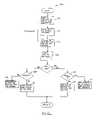
- FIG. 1shows in diagrammatic form a flash disk memory device configured in accordance with the present invention
- FIG. 2( a )shows in diagrammatic form a multimedia flash disk memory device configured in accordance with another embodiment of the present invention
- FIG. 2( b )shows in diagrammatic form an enlarged view of an erase block for the multimedia flash disk memory device of FIG. 2( a );
- FIG. 3shows in flow-chart form a process for managing data in accordance with the present invention.
- FIG. 1shows in diagrammatic form a flash disk memory device configured according to the present invention.
- the flash disk memory deviceis indicated generally by reference 10 . While the present invention is described in the context of a flash disk memory device, it will be appreciated that the invention is suitable for other memory applications.
- the flash disk memory device 10comprises control logic 11 and memory media 12 .
- the control logic 11controls the addressing of memory cells in the memory media 12 , the writing/reading of data from the memory media 12 , and the input/output interface between the flash disk memory device 10 and the external device(s) (not shown).
- the flash disk memory device 10includes a file system in accordance with the present invention and is denoted by reference 13 .
- the file system 13comprises a first volume 14 and a second volume 16 .
- the first volume 14comprises a static volume, and is configured to store relatively static files and data, i.e. data that is relatively constant and is not rewritten frequently.
- the second volume 16comprises a dynamic volume, and is configured to store dynamic data, i.e. files and data that change often. While the file system 13 is described as comprising two volumes: one volume for storing relatively static data, and another volume for storing dynamic data, it is to be appreciated that the file system may include more than one dynamic data volume.
- the second, i.e. dynamic, volume 16comprises erase blocks 18 , shown individually as 18 a , 18 b , 18 c , . . . 18 n , and metadata sectors 22 , shown individually as 22 a , 22 b , 22 c , . . . 22 m .
- Each of the erase blocks 18comprises a plurality of sectors 20 , shown individually as 20 a , 20 b , 20 c , . . . 20 s .
- the metadata sectors 22are spaced out or arranged so that each of the erase blocks 18 includes one metadata sector 22 , for example the sector 20 a shown in FIG. 1 .
- the other sectors 22e.g. 22 b to 22 s , are used to store file data. This provides an arrangement in which the loss of one erase block results in the loss of at most one metadata sector.
- the first, i.e. static, volume 14also comprises a plurality of erase blocks 24 , shown individually as 24 a , 24 b , 24 c , . . . 24 t in FIG. 1 .
- Each of the erase blocks 24comprises a plurality of sectors 26 , shown individually as 26 a , 26 b , 26 c , . . . 26 u .
- the sectors 26 in the erase blocks 24may comprise more than one or all metadata sectors 28 .
- the remaining sectors in the erase blockare utilized to store relatively static data.
- the relatively static dataincludes program executables and web pages. This arrangement allows the static volume 14 to support a higher ratio of metadata sectors to file data sectors, which in turn, is useful for storing many small files.
- FIGS. 2( a ) and 2 ( b ),show in diagrammatic form a flash disk memory device configured for a multimedia application according to another embodiment of the invention.
- the multimedia flash disk memory deviceis indicated by reference 200 .
- the multimedia flash disk memory device 200comprises a control logic module 201 and an array of memory media sectors 202 .
- the file systemcomprises a first volume 204 and a second volume 206 which are mapped into the sectors 202 on the flash disk.
- the first volume 204comprises erase blocks 205 , shown individually as 205 a , 205 b , 205 c , . . . 205 j , in FIG. 2 , and metadata sectors 209 , shown individually as 209 a , 209 b , 209 c , . . . 209 l .
- Each of the erase blocks 205comprises a plurality of sectors. The sectors are available to store one or more sectors 209 of metadata. The remaining sectors are available for storing static data, i.e. data which does not change or changes infrequently.
- the second volume 206comprises erase blocks 208 , shown individually as 208 a , 208 b , 208 c , . . . 208 n , and metadata sectors 212 , shown individually as 212 a , 212 b , 212 c , . . . 212 m .
- Each of the erase blocks 208comprises a plurality of sectors.
- the metadata sectors 212are spaced out or arranged so that each of the erase blocks 208 includes one metadata sector 212 , for example the sector 212 a shown in FIG. 2 .
- the other sectorsare used to store file data.
- the second volume 206stores a large file which is pre-allocated to hold media data from multiple messages. Then as shown in FIG. 2( a ), the large file is sub-divided into smaller allocation units 222 , shown individually as 222 a , 222 b , 222 c , . . . 222 n .
- each of the allocation units 222is allocated to an individual message.
- Each individual allocation unit 222comprises a non-media portion 224 and a media portion 226 as shown in FIG. 2( b ). Header and media data are stored in the allocation unit 222 , and the header data may occupy less than a sector as described in more detail below.
- data for the individual messageis transferred or moved between the flash disk device 200 and memory in telecommunication network or switching device (not shown) in units of the erase blocks 208 .
- a single fileuses only one inode. If all the sectors in the multimedia data file are pre-allocated during installation, there is no need for singly- and doubly-indirect sectors. This reduces the number of metadata sectors. Secondly, loosing an erase block impacts only one message. Thirdly, as messages are added or deleted, it is not necessary to constantly create and delete the files. This reduces the number of metadata accesses and the probability that a power loss will occur during a metadata access operation. Fourthly, accessing the flash memory in units of erase blocks allows a higher data transfer rate over single-sector accesses and increases efficiency.
- the allocation unit in the message fileis NE ⁇ 1 sectors.
- a metadata sector and an allocation unitfit together in one erase block.
- the message filecomprises an array of allocation units numbered starting from zero.
- a messagemay span multiple allocation units.
- a headeris maintained at the beginning of the data stored in the allocation unit.
- the remainder of the allocation unitcomprises the media payload or data.
- the headerincludes the following information fields:
- the size of the headeris less than the size of a sector.
- Free allocation units not belonging to a multimedia messagehave the invalid bits in the headers set to one and are kept on a singly-linked list using the next unit number field in the header.
- allocation units belonging to a multimedia messagehave the invalid bit fields in the headers set to zero.
- the message number fields in the headershave the same message number.
- the sequence number fieldis 0, for the second allocation unit the sequence number field is 1, and so on for the following allocation units.
- the allocation unitsare kept in sequence number order on a singly-linked list using the next number field in the headers.
- a lost erase blockcomprises an allocation unit that is part of the multimedia message
- the multimedia messageis cut into two pieces and some multimedia data is lost.
- the surviving portion of the multimedia messagemay be reconstructed by identifying the allocation units having the same message number and ordered by the sequence number.
- the lost allocation unit(s)are identified according to the missing sequence numbers. Appropriate steps may then be taken to mitigate the effects of lost multimedia data, for example, a packet loss concealment algorithm.
- a lost erase blockcomprises a free allocation unit
- the singly-linked list of free allocation unitsis cut into two pieces. The break is reparable by enumerating the allocated units and putting the remaining units on the free list.
- the operation of a file or data structure according to the present inventionis further illustrated by the following example, in which relatively static data and dynamic data are both to be stored on a flash disk memory device or other similar type of read/write mass storage device.
- the static datacomprises 100 two-sector files that do not change, for example, web site data or online help data.
- the size of the erase block(indicated by reference 24 in FIG. 1 ) is 32 sectors (indicated by reference 26 in FIG. 1 ).
- Each one of the filesincludes an inode.
- the inodeis another metadata structure, which includes information for the exact file size in bytes and the last modification time.
- each of the sectors(indicated by reference 26 in FIG. 1 ) can store four inodes.
- the two-sector filescomprise relatively static data
- the datais stored in the first or static volume (indicated by reference 14 in FIG. 1 )
- the 25 inodesare stored consecutively in 25 sectors 26 ( FIG. 1 ) of one of the erase blocks 24 , for example, 24 a ( FIG. 1 ). Accordingly, efficiencies are realized by packing the metadata into consecutive sectors 26 ( FIG. 1 ) in one of the erase blocks 24 ( FIG. 1 ) in the first volume 14 ( FIG. 1 ).
- each of the erase blocks 18includes one sector 20 , for example the sector 20 a , for storing metadata.
- 800 sectors 20i.e. 25 ⁇ 32 sectors
- the remaining sectors 20i.e. 1 to 31
- the file datacomprises 200 sectors (i.e. 100 files ⁇ 2 sectors)
- only 25.8% of the available 775 data sectorsare utilized. Therefore, efficiencies are realized by utilizing the first or static volume 14 ( FIG. 1 ) for storing static data.
- FIG. 3shows in flow-chart form a simplified process for storing data on flash disk memory media (for example, the flash disk memory device 10 of FIG. 1 ) in accordance with another aspect of the present invention.
- the processis indicated by reference 300 .
- the first step 301comprises dividing or partitioning the memory media into two volumes: a first, e.g. static, volume and a second, e.g. dynamic, volume.
- the next step 302comprises dividing each of the first and the second volumes into blocks or erase blocks, for example, with each block having 32 sectors.
- step 303for each of the erase blocks in the second volume, at least one sector is designated for reading/writing metadata.
- the steps 301 to 304may be performed as part of an initialization or formatting operation.
- memory management functions of reading, writing, and erasing dataare performed according to the data type.
- the datais classified as either static data or as dynamic data.
- Static datais data which is relatively stable and is not changed, i.e. rewritten frequently over time.
- Dynamic datais data that changes and is rewritten frequently. If the data is dynamic data as determined in decision block 306 , then the data is stored in the second volume on the memory device.
- decision block 308the dynamic data to be stored in the second, i.e. dynamic, volume is processed either as metadata or regular data.
- the datais metadata, then the data is written in the sector in one of the erase blocks allocated to metadata (block 310 ). If the data is not metadata, then the data is written to the data portion of the associated erase block (block 312 ). If the data is static data (as determined in decision block 306 ), then the data is stored in the first, i.e. static, volume. In decision block 314 , the static data is stored either as metadata or regular data. If the static data is metadata, then the data is written in a sector in the erase block or erase blocks designated for metadata (block 316 ). As described above, static data comprising metadata may be written in contiguous sectors spanning one or more erase blocks.
- the static datais not metadata
- the datais written into one of the sectors in the other erase blocks or after the last sector allocated for metadata (block 318 ). It will be appreciated that the allocation and management of the sectors and erase blocks will typically be under the control of a memory management function or controller coupled to or interfacing with the memory device.
- the operation of a process or technique for storing data on flash disk memory mediais further illustrated at an implementation level with reference to the accompanying pseudo code.
- the spacing out of metadata sectors as described aboveis implemented at a device driver level.
- the file systemissues read/write requests to the device driver, and a read/write request includes the following parameters;
- the device driverIn response to the read/write request from the file system, the device driver translates the starting sector number before passing it on to the flash memory as follows:
- NM metadata sectorsin the dynamic volume, and logically the metadata sectors occupy the beginning of the volume.
- the translation process according to the present inventionspreads the NM metadata sectors out, i.e. one metadata sector per erase block. There are NE sectors per erase block.
- a multiple sector metadata access in the dynamic volumecomprises a sequence of single sector accesses. If a single data access in the dynamic volume has to cross a metadata sector, then the single access is turned into a pair of accesses as follows:
Landscapes
- Engineering & Computer Science (AREA)
- Theoretical Computer Science (AREA)
- Physics & Mathematics (AREA)
- General Engineering & Computer Science (AREA)
- General Physics & Mathematics (AREA)
- Human Computer Interaction (AREA)
- Information Retrieval, Db Structures And Fs Structures Therefor (AREA)
- Techniques For Improving Reliability Of Storages (AREA)
Abstract
Description
- (1) read sectors N0 to N0+NE−1
- (2) clear erase block
- (3) replace sector N read in step (1) with new data
- (4) write sectors N0 to N0+NE−1
- invalid bit
- message number
- sequence number
- next unit number
- volume
- starting sector number I
- sector count N
The static volume and the dynamic volume each comprise an array of sectors, numbered starting at zero. The flash memory in turn comprises an array of sectors numbered starting from zero. The static volume begins at sector Isand the dynamic volume begins at sector ID.
| if volume is static then | ||
| I <- IS+I | ||
| else if volume is dynamic then | ||
| if I<NM then | ||
| I <- ID+I*NE | ||
| else | ||
| I <- I−NM | ||
| I <- ID+(I div (NE−1))*NE+(I mod (NE−1))+1 | ||
| end if | ||
| end if | ||
There are NM metadata sectors in the dynamic volume, and logically the metadata sectors occupy the beginning of the volume. The translation process according to the present invention spreads the NM metadata sectors out, i.e. one metadata sector per erase block. There are NE sectors per erase block.
| If (I mod NE)+N > NE then | ||
| I1 <- I | ||
| N1 <- NE−(I mod NE) | ||
| I2 <- I+N1+1 | ||
| N2 <- N−N1 | ||
| end if | ||
It will be appreciated that for this segment, the sector number I has already been translated. The first access starts at sector I1 and continues for N1 sectors. The second access starts at sector I2 and continues for N2 sectors.
| if volume is static then | ||
| I <- IS+ I | ||
| access (I,N) | ||
| else if volume is dynamic then | ||
| if I<NM Then | ||
| I <- IS+I*NE | ||
| for i from 1 to N | ||
| access(I, 1) | ||
| I <- I+NE | ||
| end for | ||
| else | ||
| I <- I−NM | ||
| I <- ID+(I div (NE−1))*NE+(I mod (NE−1))+1 | ||
| if (I mod NE)+N ,<= NE then | ||
| access(I,N) | ||
| else | ||
| I1 <- I | ||
| N1 <- NE−(I mod NE) | ||
| access(I1, N1) | ||
| I2 <- I+N1+1 | ||
| N2 <- N−N1 | ||
| access(I2, N2) | ||
| end if | ||
| end if | ||
| end if | ||
It will be understood that ‘access(I, N)’ indicates reading/writing the flash array starting at sector I for N sectors.
Claims (14)
Priority Applications (1)
| Application Number | Priority Date | Filing Date | Title |
|---|---|---|---|
| US10/734,280US7363420B2 (en) | 2003-12-15 | 2003-12-15 | Method and file structures for managing data on a flash disk |
Applications Claiming Priority (1)
| Application Number | Priority Date | Filing Date | Title |
|---|---|---|---|
| US10/734,280US7363420B2 (en) | 2003-12-15 | 2003-12-15 | Method and file structures for managing data on a flash disk |
Publications (2)
| Publication Number | Publication Date |
|---|---|
| US20050132126A1 US20050132126A1 (en) | 2005-06-16 |
| US7363420B2true US7363420B2 (en) | 2008-04-22 |
Family
ID=34653328
Family Applications (1)
| Application Number | Title | Priority Date | Filing Date |
|---|---|---|---|
| US10/734,280Expired - LifetimeUS7363420B2 (en) | 2003-12-15 | 2003-12-15 | Method and file structures for managing data on a flash disk |
Country Status (1)
| Country | Link |
|---|---|
| US (1) | US7363420B2 (en) |
Cited By (77)
| Publication number | Priority date | Publication date | Assignee | Title |
|---|---|---|---|---|
| US20080158958A1 (en)* | 2006-12-17 | 2008-07-03 | Anobit Technologies Ltd. | Memory device with reduced reading |
| US20080282106A1 (en)* | 2007-05-12 | 2008-11-13 | Anobit Technologies Ltd | Data storage with incremental redundancy |
| US20090106485A1 (en)* | 2007-10-19 | 2009-04-23 | Anobit Technologies Ltd. | Reading analog memory cells using built-in multi-threshold commands |
| US20090103358A1 (en)* | 2006-05-12 | 2009-04-23 | Anobit Technologies Ltd. | Reducing programming error in memory devices |
| US20090240872A1 (en)* | 2008-03-18 | 2009-09-24 | Anobit Technologies Ltd | Memory device with multiple-accuracy read commands |
| US20090291418A1 (en)* | 2008-05-20 | 2009-11-26 | Amit Srivastav | Navigation system |
| US7751240B2 (en) | 2007-01-24 | 2010-07-06 | Anobit Technologies Ltd. | Memory device with negative thresholds |
| US7773413B2 (en) | 2007-10-08 | 2010-08-10 | Anobit Technologies Ltd. | Reliable data storage in analog memory cells in the presence of temperature variations |
| US7821826B2 (en) | 2006-10-30 | 2010-10-26 | Anobit Technologies, Ltd. | Memory cell readout using successive approximation |
| US7864573B2 (en) | 2008-02-24 | 2011-01-04 | Anobit Technologies Ltd. | Programming analog memory cells for reduced variance after retention |
| US7900102B2 (en) | 2006-12-17 | 2011-03-01 | Anobit Technologies Ltd. | High-speed programming of memory devices |
| US7924587B2 (en) | 2008-02-21 | 2011-04-12 | Anobit Technologies Ltd. | Programming of analog memory cells using a single programming pulse per state transition |
| US7925936B1 (en) | 2007-07-13 | 2011-04-12 | Anobit Technologies Ltd. | Memory device with non-uniform programming levels |
| US7924613B1 (en) | 2008-08-05 | 2011-04-12 | Anobit Technologies Ltd. | Data storage in analog memory cells with protection against programming interruption |
| US7924648B2 (en) | 2006-11-28 | 2011-04-12 | Anobit Technologies Ltd. | Memory power and performance management |
| US7975192B2 (en) | 2006-10-30 | 2011-07-05 | Anobit Technologies Ltd. | Reading memory cells using multiple thresholds |
| US7995388B1 (en) | 2008-08-05 | 2011-08-09 | Anobit Technologies Ltd. | Data storage using modified voltages |
| US8000135B1 (en) | 2008-09-14 | 2011-08-16 | Anobit Technologies Ltd. | Estimation of memory cell read thresholds by sampling inside programming level distribution intervals |
| US8001320B2 (en) | 2007-04-22 | 2011-08-16 | Anobit Technologies Ltd. | Command interface for memory devices |
| US8000141B1 (en) | 2007-10-19 | 2011-08-16 | Anobit Technologies Ltd. | Compensation for voltage drifts in analog memory cells |
| US8050086B2 (en) | 2006-05-12 | 2011-11-01 | Anobit Technologies Ltd. | Distortion estimation and cancellation in memory devices |
| US8060806B2 (en) | 2006-08-27 | 2011-11-15 | Anobit Technologies Ltd. | Estimation of non-linear distortion in memory devices |
| US8085586B2 (en) | 2007-12-27 | 2011-12-27 | Anobit Technologies Ltd. | Wear level estimation in analog memory cells |
| US8151163B2 (en) | 2006-12-03 | 2012-04-03 | Anobit Technologies Ltd. | Automatic defect management in memory devices |
| US8151166B2 (en) | 2007-01-24 | 2012-04-03 | Anobit Technologies Ltd. | Reduction of back pattern dependency effects in memory devices |
| US8156398B2 (en) | 2008-02-05 | 2012-04-10 | Anobit Technologies Ltd. | Parameter estimation based on error correction code parity check equations |
| US8156403B2 (en) | 2006-05-12 | 2012-04-10 | Anobit Technologies Ltd. | Combined distortion estimation and error correction coding for memory devices |
| US8169825B1 (en) | 2008-09-02 | 2012-05-01 | Anobit Technologies Ltd. | Reliable data storage in analog memory cells subjected to long retention periods |
| US8174905B2 (en) | 2007-09-19 | 2012-05-08 | Anobit Technologies Ltd. | Programming orders for reducing distortion in arrays of multi-level analog memory cells |
| US8174857B1 (en) | 2008-12-31 | 2012-05-08 | Anobit Technologies Ltd. | Efficient readout schemes for analog memory cell devices using multiple read threshold sets |
| US8208304B2 (en) | 2008-11-16 | 2012-06-26 | Anobit Technologies Ltd. | Storage at M bits/cell density in N bits/cell analog memory cell devices, M>N |
| US8209588B2 (en) | 2007-12-12 | 2012-06-26 | Anobit Technologies Ltd. | Efficient interference cancellation in analog memory cell arrays |
| US8225181B2 (en) | 2007-11-30 | 2012-07-17 | Apple Inc. | Efficient re-read operations from memory devices |
| US8228701B2 (en) | 2009-03-01 | 2012-07-24 | Apple Inc. | Selective activation of programming schemes in analog memory cell arrays |
| US8230300B2 (en) | 2008-03-07 | 2012-07-24 | Apple Inc. | Efficient readout from analog memory cells using data compression |
| US8239734B1 (en) | 2008-10-15 | 2012-08-07 | Apple Inc. | Efficient data storage in storage device arrays |
| US8239735B2 (en) | 2006-05-12 | 2012-08-07 | Apple Inc. | Memory Device with adaptive capacity |
| US8238157B1 (en) | 2009-04-12 | 2012-08-07 | Apple Inc. | Selective re-programming of analog memory cells |
| US8248831B2 (en) | 2008-12-31 | 2012-08-21 | Apple Inc. | Rejuvenation of analog memory cells |
| US8261159B1 (en) | 2008-10-30 | 2012-09-04 | Apple, Inc. | Data scrambling schemes for memory devices |
| US8259497B2 (en) | 2007-08-06 | 2012-09-04 | Apple Inc. | Programming schemes for multi-level analog memory cells |
| US8259506B1 (en) | 2009-03-25 | 2012-09-04 | Apple Inc. | Database of memory read thresholds |
| US8270246B2 (en) | 2007-11-13 | 2012-09-18 | Apple Inc. | Optimized selection of memory chips in multi-chips memory devices |
| US8369141B2 (en) | 2007-03-12 | 2013-02-05 | Apple Inc. | Adaptive estimation of memory cell read thresholds |
| US8400858B2 (en) | 2008-03-18 | 2013-03-19 | Apple Inc. | Memory device with reduced sense time readout |
| US8429493B2 (en) | 2007-05-12 | 2013-04-23 | Apple Inc. | Memory device with internal signap processing unit |
| US8438195B2 (en) | 2011-02-15 | 2013-05-07 | Samsung Electronics Co., Ltd. | File system operating method and devices using the same |
| US8456905B2 (en) | 2007-12-16 | 2013-06-04 | Apple Inc. | Efficient data storage in multi-plane memory devices |
| US8479080B1 (en) | 2009-07-12 | 2013-07-02 | Apple Inc. | Adaptive over-provisioning in memory systems |
| US8482978B1 (en) | 2008-09-14 | 2013-07-09 | Apple Inc. | Estimation of memory cell read thresholds by sampling inside programming level distribution intervals |
| US8495465B1 (en) | 2009-10-15 | 2013-07-23 | Apple Inc. | Error correction coding over multiple memory pages |
| US8521781B2 (en) | 2005-12-22 | 2013-08-27 | Alan Joshua Shapiro | Apparatus and method for selective file erasure using metadata modifications |
| US8527819B2 (en) | 2007-10-19 | 2013-09-03 | Apple Inc. | Data storage in analog memory cell arrays having erase failures |
| US8572423B1 (en) | 2010-06-22 | 2013-10-29 | Apple Inc. | Reducing peak current in memory systems |
| US8572311B1 (en) | 2010-01-11 | 2013-10-29 | Apple Inc. | Redundant data storage in multi-die memory systems |
| US8595591B1 (en) | 2010-07-11 | 2013-11-26 | Apple Inc. | Interference-aware assignment of programming levels in analog memory cells |
| US8615773B2 (en) | 2011-03-31 | 2013-12-24 | Honeywell International Inc. | Systems and methods for coordinating computing functions to accomplish a task using a configuration file and standardized executable application modules |
| US8645794B1 (en) | 2010-07-31 | 2014-02-04 | Apple Inc. | Data storage in analog memory cells using a non-integer number of bits per cell |
| US8677054B1 (en) | 2009-12-16 | 2014-03-18 | Apple Inc. | Memory management schemes for non-volatile memory devices |
| US8694814B1 (en) | 2010-01-10 | 2014-04-08 | Apple Inc. | Reuse of host hibernation storage space by memory controller |
| US8694853B1 (en) | 2010-05-04 | 2014-04-08 | Apple Inc. | Read commands for reading interfering memory cells |
| US8694854B1 (en) | 2010-08-17 | 2014-04-08 | Apple Inc. | Read threshold setting based on soft readout statistics |
| US8726084B2 (en) | 2011-10-14 | 2014-05-13 | Honeywell International Inc. | Methods and systems for distributed diagnostic reasoning |
| US8751777B2 (en) | 2011-01-28 | 2014-06-10 | Honeywell International Inc. | Methods and reconfigurable systems to optimize the performance of a condition based health maintenance system |
| US8832649B2 (en) | 2012-05-22 | 2014-09-09 | Honeywell International Inc. | Systems and methods for augmenting the functionality of a monitoring node without recompiling |
| US8832354B2 (en) | 2009-03-25 | 2014-09-09 | Apple Inc. | Use of host system resources by memory controller |
| US8832716B2 (en) | 2012-08-10 | 2014-09-09 | Honeywell International Inc. | Systems and methods for limiting user customization of task workflow in a condition based health maintenance system |
| US8856475B1 (en) | 2010-08-01 | 2014-10-07 | Apple Inc. | Efficient selection of memory blocks for compaction |
| US8924661B1 (en) | 2009-01-18 | 2014-12-30 | Apple Inc. | Memory system including a controller and processors associated with memory devices |
| US8949684B1 (en) | 2008-09-02 | 2015-02-03 | Apple Inc. | Segmented data storage |
| US8990770B2 (en) | 2011-05-25 | 2015-03-24 | Honeywell International Inc. | Systems and methods to configure condition based health maintenance systems |
| US9021181B1 (en) | 2010-09-27 | 2015-04-28 | Apple Inc. | Memory management for unifying memory cell conditions by using maximum time intervals |
| US9104580B1 (en) | 2010-07-27 | 2015-08-11 | Apple Inc. | Cache memory for hybrid disk drives |
| US9959046B2 (en)* | 2015-12-30 | 2018-05-01 | Samsung Electronics Co., Ltd. | Multi-streaming mechanism to optimize journal based data storage systems on SSD |
| US11226881B2 (en)* | 2020-04-30 | 2022-01-18 | EMC IP Holding Company LLC | Responding to a fault of a disk which stores metadata and user data in different disk slices |
| US11556416B2 (en) | 2021-05-05 | 2023-01-17 | Apple Inc. | Controlling memory readout reliability and throughput by adjusting distance between read thresholds |
| US11847342B2 (en) | 2021-07-28 | 2023-12-19 | Apple Inc. | Efficient transfer of hard data and confidence levels in reading a nonvolatile memory |
Families Citing this family (14)
| Publication number | Priority date | Publication date | Assignee | Title |
|---|---|---|---|---|
| JP4415356B2 (en)* | 2002-12-24 | 2010-02-17 | エルジー エレクトロニクス インコーポレイティド | Double journaling storage method and storage medium thereof |
| US8457131B2 (en)* | 2005-02-18 | 2013-06-04 | Broadcom Corporation | Dynamic table sharing of memory space within a network device |
| US7389397B2 (en)* | 2005-06-01 | 2008-06-17 | Sandisk Il Ltd | Method of storing control information in a large-page flash memory device |
| KR100755702B1 (en)* | 2005-12-27 | 2007-09-05 | 삼성전자주식회사 | Storage device that uses non-volatile memory as cache and its operation method |
| KR100755700B1 (en)* | 2005-12-27 | 2007-09-05 | 삼성전자주식회사 | Storage device that uses non-volatile memory as cache and its management method |
| KR100874702B1 (en) | 2006-10-02 | 2008-12-18 | 삼성전자주식회사 | Device Drivers and Methods for Efficiently Managing Flash Memory File Systems |
| US8015350B2 (en)* | 2006-10-10 | 2011-09-06 | Seagate Technology Llc | Block level quality of service data in a data storage device |
| US8949506B2 (en) | 2010-07-30 | 2015-02-03 | Apple Inc. | Initiating wear leveling for a non-volatile memory |
| US11314344B2 (en) | 2010-12-03 | 2022-04-26 | Razer (Asia-Pacific) Pte. Ltd. | Haptic ecosystem |
| US8521948B2 (en)* | 2011-01-03 | 2013-08-27 | Apple Inc. | Handling dynamic and static data for a system having non-volatile memory |
| US9645917B2 (en)* | 2012-05-22 | 2017-05-09 | Netapp, Inc. | Specializing I/O access patterns for flash storage |
| US20150207669A1 (en)* | 2012-09-14 | 2015-07-23 | Telefonaktiebolaget L M Ericsson (Publ) | Data redundancy in a data layered architecture network |
| US10127236B1 (en)* | 2013-06-27 | 2018-11-13 | EMC IP Holding Company | Filesystem storing file data in larger units than used for metadata |
| CN106407129B (en)* | 2015-08-03 | 2019-12-06 | 四川效率源信息安全技术股份有限公司 | data extraction method of embedded security equipment |
Citations (5)
| Publication number | Priority date | Publication date | Assignee | Title |
|---|---|---|---|---|
| US5544356A (en)* | 1990-12-31 | 1996-08-06 | Intel Corporation | Block-erasable non-volatile semiconductor memory which tracks and stores the total number of write/erase cycles for each block |
| US6535949B1 (en)* | 1999-04-19 | 2003-03-18 | Research In Motion Limited | Portable electronic device having a log-structured file system in flash memory |
| US6536038B1 (en)* | 1999-11-29 | 2003-03-18 | Intel Corporation | Dynamic update of non-upgradeable memory |
| US20030078907A1 (en)* | 2001-10-22 | 2003-04-24 | Michael Soemo | Partially embedded database and an embedded database manager for a control system |
| US20040158638A1 (en)* | 2003-02-06 | 2004-08-12 | Peters Jay R. St. | Providing static and dynamic event data |
- 2003
- 2003-12-15USUS10/734,280patent/US7363420B2/ennot_activeExpired - Lifetime
Patent Citations (5)
| Publication number | Priority date | Publication date | Assignee | Title |
|---|---|---|---|---|
| US5544356A (en)* | 1990-12-31 | 1996-08-06 | Intel Corporation | Block-erasable non-volatile semiconductor memory which tracks and stores the total number of write/erase cycles for each block |
| US6535949B1 (en)* | 1999-04-19 | 2003-03-18 | Research In Motion Limited | Portable electronic device having a log-structured file system in flash memory |
| US6536038B1 (en)* | 1999-11-29 | 2003-03-18 | Intel Corporation | Dynamic update of non-upgradeable memory |
| US20030078907A1 (en)* | 2001-10-22 | 2003-04-24 | Michael Soemo | Partially embedded database and an embedded database manager for a control system |
| US20040158638A1 (en)* | 2003-02-06 | 2004-08-12 | Peters Jay R. St. | Providing static and dynamic event data |
Cited By (94)
| Publication number | Priority date | Publication date | Assignee | Title |
|---|---|---|---|---|
| US8782089B2 (en) | 2005-12-22 | 2014-07-15 | Alan Joshua Shapiro | Selective file erasure using metadata modifications and apparatus |
| US8521781B2 (en) | 2005-12-22 | 2013-08-27 | Alan Joshua Shapiro | Apparatus and method for selective file erasure using metadata modifications |
| US9171005B2 (en) | 2005-12-22 | 2015-10-27 | Alan Joshua Shapiro | System and method for selective file erasure using metadata modifcations |
| US8570804B2 (en) | 2006-05-12 | 2013-10-29 | Apple Inc. | Distortion estimation and cancellation in memory devices |
| US20090103358A1 (en)* | 2006-05-12 | 2009-04-23 | Anobit Technologies Ltd. | Reducing programming error in memory devices |
| US8050086B2 (en) | 2006-05-12 | 2011-11-01 | Anobit Technologies Ltd. | Distortion estimation and cancellation in memory devices |
| US8599611B2 (en) | 2006-05-12 | 2013-12-03 | Apple Inc. | Distortion estimation and cancellation in memory devices |
| US7697326B2 (en) | 2006-05-12 | 2010-04-13 | Anobit Technologies Ltd. | Reducing programming error in memory devices |
| US8156403B2 (en) | 2006-05-12 | 2012-04-10 | Anobit Technologies Ltd. | Combined distortion estimation and error correction coding for memory devices |
| US8239735B2 (en) | 2006-05-12 | 2012-08-07 | Apple Inc. | Memory Device with adaptive capacity |
| US8060806B2 (en) | 2006-08-27 | 2011-11-15 | Anobit Technologies Ltd. | Estimation of non-linear distortion in memory devices |
| US7975192B2 (en) | 2006-10-30 | 2011-07-05 | Anobit Technologies Ltd. | Reading memory cells using multiple thresholds |
| US7821826B2 (en) | 2006-10-30 | 2010-10-26 | Anobit Technologies, Ltd. | Memory cell readout using successive approximation |
| US8145984B2 (en) | 2006-10-30 | 2012-03-27 | Anobit Technologies Ltd. | Reading memory cells using multiple thresholds |
| USRE46346E1 (en) | 2006-10-30 | 2017-03-21 | Apple Inc. | Reading memory cells using multiple thresholds |
| US7924648B2 (en) | 2006-11-28 | 2011-04-12 | Anobit Technologies Ltd. | Memory power and performance management |
| US8151163B2 (en) | 2006-12-03 | 2012-04-03 | Anobit Technologies Ltd. | Automatic defect management in memory devices |
| US20080158958A1 (en)* | 2006-12-17 | 2008-07-03 | Anobit Technologies Ltd. | Memory device with reduced reading |
| US7900102B2 (en) | 2006-12-17 | 2011-03-01 | Anobit Technologies Ltd. | High-speed programming of memory devices |
| US7593263B2 (en) | 2006-12-17 | 2009-09-22 | Anobit Technologies Ltd. | Memory device with reduced reading latency |
| US7881107B2 (en) | 2007-01-24 | 2011-02-01 | Anobit Technologies Ltd. | Memory device with negative thresholds |
| US7751240B2 (en) | 2007-01-24 | 2010-07-06 | Anobit Technologies Ltd. | Memory device with negative thresholds |
| US8151166B2 (en) | 2007-01-24 | 2012-04-03 | Anobit Technologies Ltd. | Reduction of back pattern dependency effects in memory devices |
| US8369141B2 (en) | 2007-03-12 | 2013-02-05 | Apple Inc. | Adaptive estimation of memory cell read thresholds |
| US8001320B2 (en) | 2007-04-22 | 2011-08-16 | Anobit Technologies Ltd. | Command interface for memory devices |
| US8234545B2 (en) | 2007-05-12 | 2012-07-31 | Apple Inc. | Data storage with incremental redundancy |
| US20080282106A1 (en)* | 2007-05-12 | 2008-11-13 | Anobit Technologies Ltd | Data storage with incremental redundancy |
| US8429493B2 (en) | 2007-05-12 | 2013-04-23 | Apple Inc. | Memory device with internal signap processing unit |
| US7925936B1 (en) | 2007-07-13 | 2011-04-12 | Anobit Technologies Ltd. | Memory device with non-uniform programming levels |
| US8259497B2 (en) | 2007-08-06 | 2012-09-04 | Apple Inc. | Programming schemes for multi-level analog memory cells |
| US8174905B2 (en) | 2007-09-19 | 2012-05-08 | Anobit Technologies Ltd. | Programming orders for reducing distortion in arrays of multi-level analog memory cells |
| US7773413B2 (en) | 2007-10-08 | 2010-08-10 | Anobit Technologies Ltd. | Reliable data storage in analog memory cells in the presence of temperature variations |
| US8000141B1 (en) | 2007-10-19 | 2011-08-16 | Anobit Technologies Ltd. | Compensation for voltage drifts in analog memory cells |
| US8527819B2 (en) | 2007-10-19 | 2013-09-03 | Apple Inc. | Data storage in analog memory cell arrays having erase failures |
| US20090106485A1 (en)* | 2007-10-19 | 2009-04-23 | Anobit Technologies Ltd. | Reading analog memory cells using built-in multi-threshold commands |
| US8068360B2 (en) | 2007-10-19 | 2011-11-29 | Anobit Technologies Ltd. | Reading analog memory cells using built-in multi-threshold commands |
| US8270246B2 (en) | 2007-11-13 | 2012-09-18 | Apple Inc. | Optimized selection of memory chips in multi-chips memory devices |
| US8225181B2 (en) | 2007-11-30 | 2012-07-17 | Apple Inc. | Efficient re-read operations from memory devices |
| US8209588B2 (en) | 2007-12-12 | 2012-06-26 | Anobit Technologies Ltd. | Efficient interference cancellation in analog memory cell arrays |
| US8456905B2 (en) | 2007-12-16 | 2013-06-04 | Apple Inc. | Efficient data storage in multi-plane memory devices |
| US8085586B2 (en) | 2007-12-27 | 2011-12-27 | Anobit Technologies Ltd. | Wear level estimation in analog memory cells |
| US8156398B2 (en) | 2008-02-05 | 2012-04-10 | Anobit Technologies Ltd. | Parameter estimation based on error correction code parity check equations |
| US7924587B2 (en) | 2008-02-21 | 2011-04-12 | Anobit Technologies Ltd. | Programming of analog memory cells using a single programming pulse per state transition |
| US7864573B2 (en) | 2008-02-24 | 2011-01-04 | Anobit Technologies Ltd. | Programming analog memory cells for reduced variance after retention |
| US8230300B2 (en) | 2008-03-07 | 2012-07-24 | Apple Inc. | Efficient readout from analog memory cells using data compression |
| US20090240872A1 (en)* | 2008-03-18 | 2009-09-24 | Anobit Technologies Ltd | Memory device with multiple-accuracy read commands |
| US8400858B2 (en) | 2008-03-18 | 2013-03-19 | Apple Inc. | Memory device with reduced sense time readout |
| US8059457B2 (en) | 2008-03-18 | 2011-11-15 | Anobit Technologies Ltd. | Memory device with multiple-accuracy read commands |
| US20090291418A1 (en)* | 2008-05-20 | 2009-11-26 | Amit Srivastav | Navigation system |
| US9354077B2 (en) | 2008-05-20 | 2016-05-31 | Honeywell International Inc. | Navigation system |
| US8498151B1 (en) | 2008-08-05 | 2013-07-30 | Apple Inc. | Data storage in analog memory cells using modified pass voltages |
| US7924613B1 (en) | 2008-08-05 | 2011-04-12 | Anobit Technologies Ltd. | Data storage in analog memory cells with protection against programming interruption |
| US7995388B1 (en) | 2008-08-05 | 2011-08-09 | Anobit Technologies Ltd. | Data storage using modified voltages |
| US8949684B1 (en) | 2008-09-02 | 2015-02-03 | Apple Inc. | Segmented data storage |
| US8169825B1 (en) | 2008-09-02 | 2012-05-01 | Anobit Technologies Ltd. | Reliable data storage in analog memory cells subjected to long retention periods |
| US8000135B1 (en) | 2008-09-14 | 2011-08-16 | Anobit Technologies Ltd. | Estimation of memory cell read thresholds by sampling inside programming level distribution intervals |
| US8482978B1 (en) | 2008-09-14 | 2013-07-09 | Apple Inc. | Estimation of memory cell read thresholds by sampling inside programming level distribution intervals |
| US8239734B1 (en) | 2008-10-15 | 2012-08-07 | Apple Inc. | Efficient data storage in storage device arrays |
| US8261159B1 (en) | 2008-10-30 | 2012-09-04 | Apple, Inc. | Data scrambling schemes for memory devices |
| US8208304B2 (en) | 2008-11-16 | 2012-06-26 | Anobit Technologies Ltd. | Storage at M bits/cell density in N bits/cell analog memory cell devices, M>N |
| US8174857B1 (en) | 2008-12-31 | 2012-05-08 | Anobit Technologies Ltd. | Efficient readout schemes for analog memory cell devices using multiple read threshold sets |
| US8397131B1 (en) | 2008-12-31 | 2013-03-12 | Apple Inc. | Efficient readout schemes for analog memory cell devices |
| US8248831B2 (en) | 2008-12-31 | 2012-08-21 | Apple Inc. | Rejuvenation of analog memory cells |
| US8924661B1 (en) | 2009-01-18 | 2014-12-30 | Apple Inc. | Memory system including a controller and processors associated with memory devices |
| US8228701B2 (en) | 2009-03-01 | 2012-07-24 | Apple Inc. | Selective activation of programming schemes in analog memory cell arrays |
| US8832354B2 (en) | 2009-03-25 | 2014-09-09 | Apple Inc. | Use of host system resources by memory controller |
| US8259506B1 (en) | 2009-03-25 | 2012-09-04 | Apple Inc. | Database of memory read thresholds |
| US8238157B1 (en) | 2009-04-12 | 2012-08-07 | Apple Inc. | Selective re-programming of analog memory cells |
| US8479080B1 (en) | 2009-07-12 | 2013-07-02 | Apple Inc. | Adaptive over-provisioning in memory systems |
| US8495465B1 (en) | 2009-10-15 | 2013-07-23 | Apple Inc. | Error correction coding over multiple memory pages |
| US8677054B1 (en) | 2009-12-16 | 2014-03-18 | Apple Inc. | Memory management schemes for non-volatile memory devices |
| US8694814B1 (en) | 2010-01-10 | 2014-04-08 | Apple Inc. | Reuse of host hibernation storage space by memory controller |
| US8677203B1 (en) | 2010-01-11 | 2014-03-18 | Apple Inc. | Redundant data storage schemes for multi-die memory systems |
| US8572311B1 (en) | 2010-01-11 | 2013-10-29 | Apple Inc. | Redundant data storage in multi-die memory systems |
| US8694853B1 (en) | 2010-05-04 | 2014-04-08 | Apple Inc. | Read commands for reading interfering memory cells |
| US8572423B1 (en) | 2010-06-22 | 2013-10-29 | Apple Inc. | Reducing peak current in memory systems |
| US8595591B1 (en) | 2010-07-11 | 2013-11-26 | Apple Inc. | Interference-aware assignment of programming levels in analog memory cells |
| US9104580B1 (en) | 2010-07-27 | 2015-08-11 | Apple Inc. | Cache memory for hybrid disk drives |
| US8645794B1 (en) | 2010-07-31 | 2014-02-04 | Apple Inc. | Data storage in analog memory cells using a non-integer number of bits per cell |
| US8767459B1 (en) | 2010-07-31 | 2014-07-01 | Apple Inc. | Data storage in analog memory cells across word lines using a non-integer number of bits per cell |
| US8856475B1 (en) | 2010-08-01 | 2014-10-07 | Apple Inc. | Efficient selection of memory blocks for compaction |
| US8694854B1 (en) | 2010-08-17 | 2014-04-08 | Apple Inc. | Read threshold setting based on soft readout statistics |
| US9021181B1 (en) | 2010-09-27 | 2015-04-28 | Apple Inc. | Memory management for unifying memory cell conditions by using maximum time intervals |
| US8751777B2 (en) | 2011-01-28 | 2014-06-10 | Honeywell International Inc. | Methods and reconfigurable systems to optimize the performance of a condition based health maintenance system |
| US8438195B2 (en) | 2011-02-15 | 2013-05-07 | Samsung Electronics Co., Ltd. | File system operating method and devices using the same |
| US8615773B2 (en) | 2011-03-31 | 2013-12-24 | Honeywell International Inc. | Systems and methods for coordinating computing functions to accomplish a task using a configuration file and standardized executable application modules |
| US8990770B2 (en) | 2011-05-25 | 2015-03-24 | Honeywell International Inc. | Systems and methods to configure condition based health maintenance systems |
| US8726084B2 (en) | 2011-10-14 | 2014-05-13 | Honeywell International Inc. | Methods and systems for distributed diagnostic reasoning |
| US8832649B2 (en) | 2012-05-22 | 2014-09-09 | Honeywell International Inc. | Systems and methods for augmenting the functionality of a monitoring node without recompiling |
| US8832716B2 (en) | 2012-08-10 | 2014-09-09 | Honeywell International Inc. | Systems and methods for limiting user customization of task workflow in a condition based health maintenance system |
| US9959046B2 (en)* | 2015-12-30 | 2018-05-01 | Samsung Electronics Co., Ltd. | Multi-streaming mechanism to optimize journal based data storage systems on SSD |
| US11226881B2 (en)* | 2020-04-30 | 2022-01-18 | EMC IP Holding Company LLC | Responding to a fault of a disk which stores metadata and user data in different disk slices |
| US11556416B2 (en) | 2021-05-05 | 2023-01-17 | Apple Inc. | Controlling memory readout reliability and throughput by adjusting distance between read thresholds |
| US11847342B2 (en) | 2021-07-28 | 2023-12-19 | Apple Inc. | Efficient transfer of hard data and confidence levels in reading a nonvolatile memory |
Also Published As
| Publication number | Publication date |
|---|---|
| US20050132126A1 (en) | 2005-06-16 |
Similar Documents
| Publication | Publication Date | Title |
|---|---|---|
| US7363420B2 (en) | Method and file structures for managing data on a flash disk | |
| US10275361B2 (en) | Managing multiple namespaces in a non-volatile memory (NVM) | |
| US8046530B2 (en) | Process and method for erase strategy in solid state disks | |
| US7594062B2 (en) | Method for changing data of a data block in a flash memory having a mapping area, a data area and an alternative area | |
| US7395384B2 (en) | Method and apparatus for maintaining data on non-volatile memory systems | |
| US7315916B2 (en) | Scratch pad block | |
| US8321652B2 (en) | Process and method for logical-to-physical address mapping using a volatile memory device in solid state disks | |
| US5566314A (en) | Flash memory device employing unused cell arrays to update files | |
| US8706989B2 (en) | Data storage device with power-off recovery system and method thereof | |
| KR100389867B1 (en) | Flash memory management method | |
| KR100923814B1 (en) | Method and apparatus for splitting a logical block | |
| US20050015557A1 (en) | Nonvolatile memory unit with specific cache | |
| US10503425B2 (en) | Dual granularity dynamic mapping with packetized storage | |
| KR20060130084A (en) | Adaptive Mode Switching of Flash Memory Address Mapping Based on Host Usage Features | |
| US7058784B2 (en) | Method for managing access operation on nonvolatile memory and block structure thereof | |
| CN113094003A (en) | Data processing method, data storage device and electronic equipment | |
| US11334480B2 (en) | Data storage device and non-volatile memory control method | |
| CN1293404A (en) | Quick flashing decument system | |
| JP4347707B2 (en) | Information recording medium formatting method and information recording medium | |
| KR101077901B1 (en) | Apparatus and method for managing flash memory using log block unit mapping technique | |
| US8364894B2 (en) | Data update method and flash memory apparatus utilizing a cache block | |
| US10896002B2 (en) | Reverse directory structure in a garbage collection unit (GCU) | |
| KR20070031647A (en) | A method of writing compressed data to a flash memory device, a method of reading the recorded data, and a flash memory device using the method | |
| EP2323136A1 (en) | Method and apparatus for emulating byte wise programmable functionality into sector wise erasable | |
| US12039193B2 (en) | Apparatus, method and computer program for managing memory page updates within non-volatile memory |
Legal Events
| Date | Code | Title | Description |
|---|---|---|---|
| AS | Assignment | Owner name:NORTEL NETWORKS LIMITED, CANADA Free format text:ASSIGNMENT OF ASSIGNORS INTEREST;ASSIGNORS:LIN, LIN;LIN, PING;REEL/FRAME:015092/0408 Effective date:20031210 | |
| FEPP | Fee payment procedure | Free format text:PAYOR NUMBER ASSIGNED (ORIGINAL EVENT CODE: ASPN); ENTITY STATUS OF PATENT OWNER: LARGE ENTITY | |
| STCF | Information on status: patent grant | Free format text:PATENTED CASE | |
| FEPP | Fee payment procedure | Free format text:PAYOR NUMBER ASSIGNED (ORIGINAL EVENT CODE: ASPN); ENTITY STATUS OF PATENT OWNER: LARGE ENTITY Free format text:PAYER NUMBER DE-ASSIGNED (ORIGINAL EVENT CODE: RMPN); ENTITY STATUS OF PATENT OWNER: LARGE ENTITY | |
| AS | Assignment | Owner name:CITIBANK, N.A., AS ADMINISTRATIVE AGENT,NEW YORK Free format text:SECURITY AGREEMENT;ASSIGNOR:AVAYA INC.;REEL/FRAME:023892/0500 Effective date:20100129 Owner name:CITIBANK, N.A., AS ADMINISTRATIVE AGENT, NEW YORK Free format text:SECURITY AGREEMENT;ASSIGNOR:AVAYA INC.;REEL/FRAME:023892/0500 Effective date:20100129 | |
| AS | Assignment | Owner name:CITICORP USA, INC., AS ADMINISTRATIVE AGENT, NEW YORK Free format text:SECURITY AGREEMENT;ASSIGNOR:AVAYA INC.;REEL/FRAME:023905/0001 Effective date:20100129 Owner name:CITICORP USA, INC., AS ADMINISTRATIVE AGENT,NEW YO Free format text:SECURITY AGREEMENT;ASSIGNOR:AVAYA INC.;REEL/FRAME:023905/0001 Effective date:20100129 Owner name:CITICORP USA, INC., AS ADMINISTRATIVE AGENT, NEW Y Free format text:SECURITY AGREEMENT;ASSIGNOR:AVAYA INC.;REEL/FRAME:023905/0001 Effective date:20100129 | |
| AS | Assignment | Owner name:AVAYA INC.,NEW JERSEY Free format text:ASSIGNMENT OF ASSIGNORS INTEREST;ASSIGNOR:NORTEL NETWORKS LIMITED;REEL/FRAME:023998/0878 Effective date:20091218 Owner name:AVAYA INC., NEW JERSEY Free format text:ASSIGNMENT OF ASSIGNORS INTEREST;ASSIGNOR:NORTEL NETWORKS LIMITED;REEL/FRAME:023998/0878 Effective date:20091218 | |
| AS | Assignment | Owner name:BANK OF NEW YORK MELLON TRUST, NA, AS NOTES COLLATERAL AGENT, THE, PENNSYLVANIA Free format text:SECURITY AGREEMENT;ASSIGNOR:AVAYA INC., A DELAWARE CORPORATION;REEL/FRAME:025863/0535 Effective date:20110211 Owner name:BANK OF NEW YORK MELLON TRUST, NA, AS NOTES COLLAT Free format text:SECURITY AGREEMENT;ASSIGNOR:AVAYA INC., A DELAWARE CORPORATION;REEL/FRAME:025863/0535 Effective date:20110211 | |
| FPAY | Fee payment | Year of fee payment:4 | |
| AS | Assignment | Owner name:BANK OF NEW YORK MELLON TRUST COMPANY, N.A., THE, PENNSYLVANIA Free format text:SECURITY AGREEMENT;ASSIGNOR:AVAYA, INC.;REEL/FRAME:030083/0639 Effective date:20130307 Owner name:BANK OF NEW YORK MELLON TRUST COMPANY, N.A., THE, Free format text:SECURITY AGREEMENT;ASSIGNOR:AVAYA, INC.;REEL/FRAME:030083/0639 Effective date:20130307 | |
| FPAY | Fee payment | Year of fee payment:8 | |
| AS | Assignment | Owner name:CITIBANK, N.A., AS ADMINISTRATIVE AGENT, NEW YORK Free format text:SECURITY INTEREST;ASSIGNORS:AVAYA INC.;AVAYA INTEGRATED CABINET SOLUTIONS INC.;OCTEL COMMUNICATIONS CORPORATION;AND OTHERS;REEL/FRAME:041576/0001 Effective date:20170124 | |
| AS | Assignment | Owner name:AVAYA INTEGRATED CABINET SOLUTIONS INC., CALIFORNIA Free format text:BANKRUPTCY COURT ORDER RELEASING ALL LIENS INCLUDING THE SECURITY INTEREST RECORDED AT REEL/FRAME 041576/0001;ASSIGNOR:CITIBANK, N.A.;REEL/FRAME:044893/0531 Effective date:20171128 Owner name:OCTEL COMMUNICATIONS LLC (FORMERLY KNOWN AS OCTEL COMMUNICATIONS CORPORATION), CALIFORNIA Free format text:BANKRUPTCY COURT ORDER RELEASING ALL LIENS INCLUDING THE SECURITY INTEREST RECORDED AT REEL/FRAME 041576/0001;ASSIGNOR:CITIBANK, N.A.;REEL/FRAME:044893/0531 Effective date:20171128 Owner name:AVAYA INC., CALIFORNIA Free format text:BANKRUPTCY COURT ORDER RELEASING ALL LIENS INCLUDING THE SECURITY INTEREST RECORDED AT REEL/FRAME 025863/0535;ASSIGNOR:THE BANK OF NEW YORK MELLON TRUST, NA;REEL/FRAME:044892/0001 Effective date:20171128 Owner name:AVAYA INC., CALIFORNIA Free format text:BANKRUPTCY COURT ORDER RELEASING ALL LIENS INCLUDING THE SECURITY INTEREST RECORDED AT REEL/FRAME 023892/0500;ASSIGNOR:CITIBANK, N.A.;REEL/FRAME:044891/0564 Effective date:20171128 Owner name:OCTEL COMMUNICATIONS LLC (FORMERLY KNOWN AS OCTEL Free format text:BANKRUPTCY COURT ORDER RELEASING ALL LIENS INCLUDING THE SECURITY INTEREST RECORDED AT REEL/FRAME 041576/0001;ASSIGNOR:CITIBANK, N.A.;REEL/FRAME:044893/0531 Effective date:20171128 Owner name:AVAYA INTEGRATED CABINET SOLUTIONS INC., CALIFORNI Free format text:BANKRUPTCY COURT ORDER RELEASING ALL LIENS INCLUDING THE SECURITY INTEREST RECORDED AT REEL/FRAME 041576/0001;ASSIGNOR:CITIBANK, N.A.;REEL/FRAME:044893/0531 Effective date:20171128 Owner name:AVAYA INC., CALIFORNIA Free format text:BANKRUPTCY COURT ORDER RELEASING ALL LIENS INCLUDING THE SECURITY INTEREST RECORDED AT REEL/FRAME 041576/0001;ASSIGNOR:CITIBANK, N.A.;REEL/FRAME:044893/0531 Effective date:20171128 Owner name:VPNET TECHNOLOGIES, INC., CALIFORNIA Free format text:BANKRUPTCY COURT ORDER RELEASING ALL LIENS INCLUDING THE SECURITY INTEREST RECORDED AT REEL/FRAME 041576/0001;ASSIGNOR:CITIBANK, N.A.;REEL/FRAME:044893/0531 Effective date:20171128 Owner name:AVAYA INC., CALIFORNIA Free format text:BANKRUPTCY COURT ORDER RELEASING ALL LIENS INCLUDING THE SECURITY INTEREST RECORDED AT REEL/FRAME 030083/0639;ASSIGNOR:THE BANK OF NEW YORK MELLON TRUST COMPANY, N.A.;REEL/FRAME:045012/0666 Effective date:20171128 | |
| AS | Assignment | Owner name:GOLDMAN SACHS BANK USA, AS COLLATERAL AGENT, NEW YORK Free format text:SECURITY INTEREST;ASSIGNORS:AVAYA INC.;AVAYA INTEGRATED CABINET SOLUTIONS LLC;OCTEL COMMUNICATIONS LLC;AND OTHERS;REEL/FRAME:045034/0001 Effective date:20171215 Owner name:GOLDMAN SACHS BANK USA, AS COLLATERAL AGENT, NEW Y Free format text:SECURITY INTEREST;ASSIGNORS:AVAYA INC.;AVAYA INTEGRATED CABINET SOLUTIONS LLC;OCTEL COMMUNICATIONS LLC;AND OTHERS;REEL/FRAME:045034/0001 Effective date:20171215 | |
| AS | Assignment | Owner name:AVAYA, INC., CALIFORNIA Free format text:RELEASE BY SECURED PARTY;ASSIGNOR:CITICORP USA, INC.;REEL/FRAME:045045/0564 Effective date:20171215 Owner name:SIERRA HOLDINGS CORP., NEW JERSEY Free format text:RELEASE BY SECURED PARTY;ASSIGNOR:CITICORP USA, INC.;REEL/FRAME:045045/0564 Effective date:20171215 | |
| AS | Assignment | Owner name:CITIBANK, N.A., AS COLLATERAL AGENT, NEW YORK Free format text:SECURITY INTEREST;ASSIGNORS:AVAYA INC.;AVAYA INTEGRATED CABINET SOLUTIONS LLC;OCTEL COMMUNICATIONS LLC;AND OTHERS;REEL/FRAME:045124/0026 Effective date:20171215 | |
| MAFP | Maintenance fee payment | Free format text:PAYMENT OF MAINTENANCE FEE, 12TH YEAR, LARGE ENTITY (ORIGINAL EVENT CODE: M1553); ENTITY STATUS OF PATENT OWNER: LARGE ENTITY Year of fee payment:12 | |
| AS | Assignment | Owner name:WILMINGTON TRUST, NATIONAL ASSOCIATION, MINNESOTA Free format text:SECURITY INTEREST;ASSIGNORS:AVAYA INC.;AVAYA MANAGEMENT L.P.;INTELLISIST, INC.;AND OTHERS;REEL/FRAME:053955/0436 Effective date:20200925 | |
| AS | Assignment | Owner name:WILMINGTON TRUST, NATIONAL ASSOCIATION, AS COLLATERAL AGENT, DELAWARE Free format text:INTELLECTUAL PROPERTY SECURITY AGREEMENT;ASSIGNORS:AVAYA INC.;INTELLISIST, INC.;AVAYA MANAGEMENT L.P.;AND OTHERS;REEL/FRAME:061087/0386 Effective date:20220712 | |
| AS | Assignment | Owner name:AVAYA INTEGRATED CABINET SOLUTIONS LLC, NEW JERSEY Free format text:RELEASE OF SECURITY INTEREST IN PATENTS AT REEL 45124/FRAME 0026;ASSIGNOR:CITIBANK, N.A., AS COLLATERAL AGENT;REEL/FRAME:063457/0001 Effective date:20230403 Owner name:AVAYA MANAGEMENT L.P., NEW JERSEY Free format text:RELEASE OF SECURITY INTEREST IN PATENTS AT REEL 45124/FRAME 0026;ASSIGNOR:CITIBANK, N.A., AS COLLATERAL AGENT;REEL/FRAME:063457/0001 Effective date:20230403 Owner name:AVAYA INC., NEW JERSEY Free format text:RELEASE OF SECURITY INTEREST IN PATENTS AT REEL 45124/FRAME 0026;ASSIGNOR:CITIBANK, N.A., AS COLLATERAL AGENT;REEL/FRAME:063457/0001 Effective date:20230403 Owner name:AVAYA HOLDINGS CORP., NEW JERSEY Free format text:RELEASE OF SECURITY INTEREST IN PATENTS AT REEL 45124/FRAME 0026;ASSIGNOR:CITIBANK, N.A., AS COLLATERAL AGENT;REEL/FRAME:063457/0001 Effective date:20230403 | |
| AS | Assignment | Owner name:WILMINGTON SAVINGS FUND SOCIETY, FSB (COLLATERAL AGENT), DELAWARE Free format text:INTELLECTUAL PROPERTY SECURITY AGREEMENT;ASSIGNORS:AVAYA MANAGEMENT L.P.;AVAYA INC.;INTELLISIST, INC.;AND OTHERS;REEL/FRAME:063742/0001 Effective date:20230501 | |
| AS | Assignment | Owner name:CITIBANK, N.A., AS COLLATERAL AGENT, NEW YORK Free format text:INTELLECTUAL PROPERTY SECURITY AGREEMENT;ASSIGNORS:AVAYA INC.;AVAYA MANAGEMENT L.P.;INTELLISIST, INC.;REEL/FRAME:063542/0662 Effective date:20230501 | |
| AS | Assignment | Owner name:AVAYA MANAGEMENT L.P., NEW JERSEY Free format text:RELEASE OF SECURITY INTEREST IN PATENTS (REEL/FRAME 045034/0001);ASSIGNOR:GOLDMAN SACHS BANK USA., AS COLLATERAL AGENT;REEL/FRAME:063779/0622 Effective date:20230501 Owner name:CAAS TECHNOLOGIES, LLC, NEW JERSEY Free format text:RELEASE OF SECURITY INTEREST IN PATENTS (REEL/FRAME 045034/0001);ASSIGNOR:GOLDMAN SACHS BANK USA., AS COLLATERAL AGENT;REEL/FRAME:063779/0622 Effective date:20230501 Owner name:HYPERQUALITY II, LLC, NEW JERSEY Free format text:RELEASE OF SECURITY INTEREST IN PATENTS (REEL/FRAME 045034/0001);ASSIGNOR:GOLDMAN SACHS BANK USA., AS COLLATERAL AGENT;REEL/FRAME:063779/0622 Effective date:20230501 Owner name:HYPERQUALITY, INC., NEW JERSEY Free format text:RELEASE OF SECURITY INTEREST IN PATENTS (REEL/FRAME 045034/0001);ASSIGNOR:GOLDMAN SACHS BANK USA., AS COLLATERAL AGENT;REEL/FRAME:063779/0622 Effective date:20230501 Owner name:ZANG, INC. (FORMER NAME OF AVAYA CLOUD INC.), NEW JERSEY Free format text:RELEASE OF SECURITY INTEREST IN PATENTS (REEL/FRAME 045034/0001);ASSIGNOR:GOLDMAN SACHS BANK USA., AS COLLATERAL AGENT;REEL/FRAME:063779/0622 Effective date:20230501 Owner name:VPNET TECHNOLOGIES, INC., NEW JERSEY Free format text:RELEASE OF SECURITY INTEREST IN PATENTS (REEL/FRAME 045034/0001);ASSIGNOR:GOLDMAN SACHS BANK USA., AS COLLATERAL AGENT;REEL/FRAME:063779/0622 Effective date:20230501 Owner name:OCTEL COMMUNICATIONS LLC, NEW JERSEY Free format text:RELEASE OF SECURITY INTEREST IN PATENTS (REEL/FRAME 045034/0001);ASSIGNOR:GOLDMAN SACHS BANK USA., AS COLLATERAL AGENT;REEL/FRAME:063779/0622 Effective date:20230501 Owner name:AVAYA INTEGRATED CABINET SOLUTIONS LLC, NEW JERSEY Free format text:RELEASE OF SECURITY INTEREST IN PATENTS (REEL/FRAME 045034/0001);ASSIGNOR:GOLDMAN SACHS BANK USA., AS COLLATERAL AGENT;REEL/FRAME:063779/0622 Effective date:20230501 Owner name:INTELLISIST, INC., NEW JERSEY Free format text:RELEASE OF SECURITY INTEREST IN PATENTS (REEL/FRAME 045034/0001);ASSIGNOR:GOLDMAN SACHS BANK USA., AS COLLATERAL AGENT;REEL/FRAME:063779/0622 Effective date:20230501 Owner name:AVAYA INC., NEW JERSEY Free format text:RELEASE OF SECURITY INTEREST IN PATENTS (REEL/FRAME 045034/0001);ASSIGNOR:GOLDMAN SACHS BANK USA., AS COLLATERAL AGENT;REEL/FRAME:063779/0622 Effective date:20230501 Owner name:AVAYA INTEGRATED CABINET SOLUTIONS LLC, NEW JERSEY Free format text:RELEASE OF SECURITY INTEREST IN PATENTS (REEL/FRAME 53955/0436);ASSIGNOR:WILMINGTON TRUST, NATIONAL ASSOCIATION, AS NOTES COLLATERAL AGENT;REEL/FRAME:063705/0023 Effective date:20230501 Owner name:INTELLISIST, INC., NEW JERSEY Free format text:RELEASE OF SECURITY INTEREST IN PATENTS (REEL/FRAME 53955/0436);ASSIGNOR:WILMINGTON TRUST, NATIONAL ASSOCIATION, AS NOTES COLLATERAL AGENT;REEL/FRAME:063705/0023 Effective date:20230501 Owner name:AVAYA INC., NEW JERSEY Free format text:RELEASE OF SECURITY INTEREST IN PATENTS (REEL/FRAME 53955/0436);ASSIGNOR:WILMINGTON TRUST, NATIONAL ASSOCIATION, AS NOTES COLLATERAL AGENT;REEL/FRAME:063705/0023 Effective date:20230501 Owner name:AVAYA MANAGEMENT L.P., NEW JERSEY Free format text:RELEASE OF SECURITY INTEREST IN PATENTS (REEL/FRAME 53955/0436);ASSIGNOR:WILMINGTON TRUST, NATIONAL ASSOCIATION, AS NOTES COLLATERAL AGENT;REEL/FRAME:063705/0023 Effective date:20230501 Owner name:AVAYA INTEGRATED CABINET SOLUTIONS LLC, NEW JERSEY Free format text:RELEASE OF SECURITY INTEREST IN PATENTS (REEL/FRAME 61087/0386);ASSIGNOR:WILMINGTON TRUST, NATIONAL ASSOCIATION, AS NOTES COLLATERAL AGENT;REEL/FRAME:063690/0359 Effective date:20230501 Owner name:INTELLISIST, INC., NEW JERSEY Free format text:RELEASE OF SECURITY INTEREST IN PATENTS (REEL/FRAME 61087/0386);ASSIGNOR:WILMINGTON TRUST, NATIONAL ASSOCIATION, AS NOTES COLLATERAL AGENT;REEL/FRAME:063690/0359 Effective date:20230501 Owner name:AVAYA INC., NEW JERSEY Free format text:RELEASE OF SECURITY INTEREST IN PATENTS (REEL/FRAME 61087/0386);ASSIGNOR:WILMINGTON TRUST, NATIONAL ASSOCIATION, AS NOTES COLLATERAL AGENT;REEL/FRAME:063690/0359 Effective date:20230501 Owner name:AVAYA MANAGEMENT L.P., NEW JERSEY Free format text:RELEASE OF SECURITY INTEREST IN PATENTS (REEL/FRAME 61087/0386);ASSIGNOR:WILMINGTON TRUST, NATIONAL ASSOCIATION, AS NOTES COLLATERAL AGENT;REEL/FRAME:063690/0359 Effective date:20230501 | |
| AS | Assignment | Owner name:AVAYA LLC, DELAWARE Free format text:(SECURITY INTEREST) GRANTOR'S NAME CHANGE;ASSIGNOR:AVAYA INC.;REEL/FRAME:065019/0231 Effective date:20230501 |