US7362616B2 - NAND flash memory with erase verify based on shorter evaluation time - Google Patents
NAND flash memory with erase verify based on shorter evaluation timeDownload PDFInfo
- Publication number
- US7362616B2 US7362616B2US11/495,886US49588606AUS7362616B2US 7362616 B2US7362616 B2US 7362616B2US 49588606 AUS49588606 AUS 49588606AUS 7362616 B2US7362616 B2US 7362616B2
- Authority
- US
- United States
- Prior art keywords
- threshold
- voltage
- reading
- range
- memory cell
- Prior art date
- Legal status (The legal status is an assumption and is not a legal conclusion. Google has not performed a legal analysis and makes no representation as to the accuracy of the status listed.)
- Active
Links
- 230000015654memoryEffects0.000titleclaimsabstractdescription70
- 238000011156evaluationMethods0.000titledescription21
- 238000000034methodMethods0.000claimsdescription30
- 230000008878couplingEffects0.000claimsdescription7
- 238000010168coupling processMethods0.000claimsdescription7
- 238000005859coupling reactionMethods0.000claimsdescription7
- 230000003247decreasing effectEffects0.000claims1
- 238000009877renderingMethods0.000claims1
- 230000004044responseEffects0.000claims1
- 238000009826distributionMethods0.000description8
- 238000007599dischargingMethods0.000description6
- 239000003990capacitorSubstances0.000description3
- 238000010586diagramMethods0.000description3
- 235000004257Cordia myxaNutrition0.000description2
- 244000157795Cordia myxaSpecies0.000description2
- 230000008901benefitEffects0.000description2
- 210000000746body regionAnatomy0.000description2
- 230000001808coupling effectEffects0.000description2
- 239000011159matrix materialSubstances0.000description2
- 238000012986modificationMethods0.000description2
- 230000004048modificationEffects0.000description2
- 239000004065semiconductorSubstances0.000description2
- 230000032683agingEffects0.000description1
- 230000004075alterationEffects0.000description1
- 230000001419dependent effectEffects0.000description1
- 230000000694effectsEffects0.000description1
- PWPJGUXAGUPAHP-UHFFFAOYSA-NlufenuronChemical compoundC1=C(Cl)C(OC(F)(F)C(C(F)(F)F)F)=CC(Cl)=C1NC(=O)NC(=O)C1=C(F)C=CC=C1FPWPJGUXAGUPAHP-UHFFFAOYSA-N0.000description1
- 239000000463materialSubstances0.000description1
- 230000008569processEffects0.000description1
- 230000000717retained effectEffects0.000description1
- 230000003068static effectEffects0.000description1
- 238000006467substitution reactionMethods0.000description1
- 239000002699waste materialSubstances0.000description1
Images


Classifications
- G—PHYSICS
- G11—INFORMATION STORAGE
- G11C—STATIC STORES
- G11C16/00—Erasable programmable read-only memories
- G11C16/02—Erasable programmable read-only memories electrically programmable
- G11C16/06—Auxiliary circuits, e.g. for writing into memory
- G11C16/10—Programming or data input circuits
- G11C16/12—Programming voltage switching circuits
- G—PHYSICS
- G11—INFORMATION STORAGE
- G11C—STATIC STORES
- G11C11/00—Digital stores characterised by the use of particular electric or magnetic storage elements; Storage elements therefor
- G11C11/56—Digital stores characterised by the use of particular electric or magnetic storage elements; Storage elements therefor using storage elements with more than two stable states represented by steps, e.g. of voltage, current, phase, frequency
- G11C11/5621—Digital stores characterised by the use of particular electric or magnetic storage elements; Storage elements therefor using storage elements with more than two stable states represented by steps, e.g. of voltage, current, phase, frequency using charge storage in a floating gate
- G11C11/5628—Programming or writing circuits; Data input circuits
- G—PHYSICS
- G11—INFORMATION STORAGE
- G11C—STATIC STORES
- G11C16/00—Erasable programmable read-only memories
- G11C16/02—Erasable programmable read-only memories electrically programmable
- G11C16/04—Erasable programmable read-only memories electrically programmable using variable threshold transistors, e.g. FAMOS
- G11C16/0483—Erasable programmable read-only memories electrically programmable using variable threshold transistors, e.g. FAMOS comprising cells having several storage transistors connected in series
- G—PHYSICS
- G11—INFORMATION STORAGE
- G11C—STATIC STORES
- G11C2211/00—Indexing scheme relating to digital stores characterized by the use of particular electric or magnetic storage elements; Storage elements therefor
- G11C2211/56—Indexing scheme relating to G11C11/56 and sub-groups for features not covered by these groups
- G11C2211/562—Multilevel memory programming aspects
- G11C2211/5621—Multilevel programming verification
- G—PHYSICS
- G11—INFORMATION STORAGE
- G11C—STATIC STORES
- G11C2211/00—Indexing scheme relating to digital stores characterized by the use of particular electric or magnetic storage elements; Storage elements therefor
- G11C2211/56—Indexing scheme relating to G11C11/56 and sub-groups for features not covered by these groups
- G11C2211/564—Miscellaneous aspects
- G11C2211/5642—Multilevel memory with buffers, latches, registers at input or output
- G—PHYSICS
- G11—INFORMATION STORAGE
- G11C—STATIC STORES
- G11C2216/00—Indexing scheme relating to G11C16/00 and subgroups, for features not directly covered by these groups
- G11C2216/12—Reading and writing aspects of erasable programmable read-only memories
- G11C2216/14—Circuits or methods to write a page or sector of information simultaneously into a nonvolatile memory, typically a complete row or word line in flash memory
Definitions
- An embodiment of the present inventionrelates to the field of non-volatile memory devices. More specifically, an embodiment of the present invention relates to the reading of a non-volatile memory device.
- Non-volatile memory devicesare used in a number of applications, whenever data must be retained even if a power supply is off.
- Flash memoriesare a particular type of non-volatile memory device, in which each cell can be electrically programmed, but a large number of cells (which form a sector) must be erased at the same time.
- each cellis formed by a floating gate MOS transistor that stores a logic level defined by its threshold voltage (which depends on the electric charge stored in the corresponding floating gate).
- the cellsare arranged in strings, each one consisting of a set of cells connected in series.
- An advantage of this architectureis the reduced area occupation (essentially due to the low number of electrical contacts and to the small size of the cells). This makes the NAND memory devices particularly advantageous in a number of applications (for example, for memory cards).
- the cells of a selected sectorare generally erased by applying a single blind erasing pulse, which is dimensioned so as to lower their threshold voltages below a reference reading voltage (typically, 0V).
- a reference reading voltagetypically, 0V.
- the NAND memory devicesimplement a decoding system that is able to bias the various cells selectively with positive voltages only (i.e., equal or higher than zero).
- a problem of the NAND memory devicesis due to the capacitive coupling between the floating gates of adjacent cells; such effect may make the threshold voltage of each cell dependent on the electric charge stored in the floating gates of the adjacent cells.
- the capacitive coupling effectmodifies the threshold voltage of each cell whenever the adjacent cells are programmed.
- the suffered variationincreases with the increment of the threshold voltages of the adjacent cells during the programming operation.
- the problemis particularly serious when the adjacent cells to be programmed start from very low threshold voltages. As a result, this variation may cause errors during the reading operations.
- the threshold voltages of the erased cellsIn order to limit the capacitive coupling effect, it would be desirable to increase the threshold voltages of the erased cells; for example, it is possible to shift the threshold voltages of the erased cells by applying a soft programming pulse (of reduced amplitude and duration). However, after this operation it is necessary to verify that the cells are still erased. For this purpose, the cells should be read with respect to the reading voltage with a negative margin (so as to ensure that they are not approaching the reading voltage beyond a safety limit).
- An embodiment of the present inventionproposes a solution, which is based on the idea of emulating multiple reference voltages during a reading operation by using different reading times.
- an embodiment of the present inventionproposes a non-volatile memory device.
- the memory deviceincludes a plurality of memory cells, each one having a programmable threshold voltage.
- the memory devicefurther includes means for reading a set of selected memory cells (such a page) with respect to a plurality of reference voltages.
- the means for readingincludes means for charging a reading node associated with the selected memory cell (such as its bit line) with a charging voltage.
- Means for biasing the selected memory cell with a biasing voltageis provided.
- meansis available for connecting the charged reading node with the biased selected memory cell.
- Meansis used for sensing a voltage at the reading node after a predefined delay from the connection.
- the biasing voltageis equal to the first reference voltage, and the delay is a common first delay.
- the biasing voltageis a second biasing voltage different from the second reference voltage (such as 0V), and the delay is a second delay different from the first delay.
- a shorter delayis used.
- the second biasing voltagemay be equal to the first reference voltage.
- the selected cellsare read with respect to a third reference voltage by applying a third biasing voltage (different from the second biasing voltage), but using the same delay.
- each biasing voltagehas a predefined sign (such as positive) or a null value, while the second and/or the third reference voltage has the opposite sign (such as negative).
- the first reference voltageis a reading voltage (such as 0V)
- the second reference voltageis the reading voltage with a margin (such as ⁇ 1V)
- the third reference voltageis the reading voltage with a lower margin (such as ⁇ 0.5V).
- the proposed solutionis used for soft-programming the erased cells so as to shift their threshold voltages towards the reading voltage until they reach the second reference voltage (i.e., ⁇ 1V).
- the proposed solutionmay be applied to a non-volatile memory device with NAND architecture.
- the threshold voltages of the soft-programmed cellsare still lower than the third reference voltage (i.e., ⁇ 0.5V).
- Another embodiment of the present inventionprovides a corresponding method for reading a non-volatile memory device.
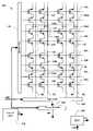
- FIG. 1is a schematic block diagram of a memory device in which the solution according to an embodiment of the invention can be used.
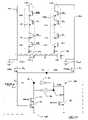
- FIG. 2Adetails a portion of the memory device of FIG. 1 .
- FIG. 2Bshows exemplificative time diagrams relating to operation of this portion of the memory device in FIG. 2A according to an embodiment of the invention.
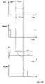
- FIG. 3shows illustrative time diagrams explaining the principle on which the solution according to an embodiment of the present invention is based.
- FIG. 4shows a flow chart describing an erasing procedure of the memory device according to an embodiment of the present invention.
- FIGS. 5A through 5Dare exemplificative representations of various distributions of the threshold voltages of the erased cells according to an embodiment of the present invention.
- the memory device 100includes a matrix of cells 110 , typically realized by floating-gate MOS transistors.
- the matrixincludes one or more sectors 115 , each one being individually erasable; in particular, all the cells 110 are formed in a common body region of a chip of semiconductor material (wherein the memory device 100 is integrated).
- each cell 110has a low threshold voltage (to which a logic level “1” is typically associated).
- the cell 110is programmed by injecting electrons into its floating-gate; in this condition the cell 110 has a high threshold voltage (to which a logic level “0” is typically associated). Therefore, when the cell 110 is biased for reading, it is conductive if erased or it is non-conductive if programmed.
- each sector 115includes a plurality of strings 125 ; each string 125 is formed by a set of cells 110 (typically 16) that are connected in series between two select transistors 120 s and 120 d.
- an intermediate cell 110 of the string 125has the drain terminal connected to the source terminal of the upper cell 110 and the source terminal connected to the drain terminal of the lower cell 110 .
- the lowest cell 110 of the string 125has the source terminal connected to the drain terminal of the select transistor 120 s
- the uppermost cell 110 of the string 125has the drain terminal connected to the source terminal of the select transistor 120 d .
- the select transistor 120 shas the source terminal connected to the source terminal of the select transistor 120 s of a lower string
- the transistor 120 dhas the drain terminal connected to the drain terminal of the select transistor 120 d of an upper string.
- the gate terminals of the cells 110 of each roware connected to a corresponding word line WL.
- the drain terminals of the select transistors 120 d of the strings of each columnare connected to a corresponding bit line BL.
- the gate terminals of the select transistors 120 d positioned on a same roware connected to a corresponding drain select line DSL; likewise, the gate terminals of the select transistors 120 s positioned on a same row are connected to a corresponding source select line SSL.
- the source terminals of all the select transistors 120 sare connected to a common source line SL, which is typically maintained at a reference voltage (or ground).
- the cells 110 belonging to each roware logically grouped in two pages; in detail, a first page is formed by the cells 110 having an even position and a second page is formed by the cells having an odd position.
- the memory device 100receives an address ADR for selecting a desired page. A portion of the address ADR is supplied to a row decoder 130 that selects the word line WL of the desired page, and the drain select line DSL and the source select line SSL of the corresponding strings 125 . Another portion of the address ADR (1 bit) is supplied to a page buffer 140 . The page buffer 140 selects the bit lines BL of the desired page, that is, the even ones or the odd ones; the page buffer 140 then reads (or writes) the cells 110 of the selected page. The page buffer 140 interfaces with a column decoder 150 ; the column decoder 150 receives a further portion of the address ADR, and outputs a corresponding word DT selected in the page that has been read by the page buffer 140 .
- the memory device 100further includes a power management unit (PMU) 160 and a control unit 170 .
- the PMU 160supplies the voltages that are used for performing the various operations on the memory device 100 , for example, from approximately 0V to approximately 20V (referred to as a whole with Vin); the voltages Vin are generated (for example, through charge pumps) starting from a power supply voltage Vdd supplied from the outside (typically, 1.8/3V).
- the control unit 170provides the control signals (referred to as a whole with Sc) that are used for driving the various components of the memory device 100 .
- the page buffer 140includes a read unit for each pair of (even and odd) bit lines (the components used for writing the selected cells are omitted for sake of simplicity).
- a selected stringis denoted with 125 s and an unselected string is denoted with 125 u (from now on, the suffixes “s” and “u” will be added to the references of the circuital components to discriminate the ones associated with the selected string 125 s from the ones associated with the unselected string 125 u ).
- the strings 125 s and 125 uhave the source lines SLs and SLu connected to a ground terminal.
- Two NMOS transistors Ndu and Ndsare used for discharging the bit lines BLu and BLs, respectively.
- the NMOS transistors Ndu and Ndshave the source terminal and the drain terminal, respectively, that are connected together to the ground terminal.
- the NMOS transistor Ndshas the drain terminal connected to the bit line BLs, whereas the NMOS transistor Ndu has the source terminal connected to the bit line BLU.
- the NMOS transistors Nds and Ndureceive at their gate terminals discharging voltages Vds and Vdu, respectively.
- the stray capacitances of the bit lines BLs and BLuare represented by corresponding capacitors C BL s and C BL u, connected between the drain terminal of the NMOS transistor Ns and Nu, respectively, and the ground terminal.
- the page buffer 140includes a PMOS transistor Pc that is used to pre-charge the node 210 at the beginning of the reading operation.
- the transistor Pchas the drain terminal connected to the node 210 and the source terminal connected to a terminal providing a pre-charging voltage Vc (for example, 2.1V).
- the gate terminal of the PMOS transistor Pcreceives a pre-charging signal PRECH (from the Control Unit); the pre-charging signal PRECH is underlined to denote that it is asserted at the low logic level (for example, ground) and deasserted at the high logic level (for example, Vdd).
- the page buffer 140further includes a latch 220 that is used to read the logic level stored in the selected cell 110 .
- the latch 220is formed by two inverters D 1 and D 2 .
- the input terminal of the inverter D 1 and the output terminal of the inverter D 2are connected together to define an input node IN of the latch 220 ; likewise, the output terminal of the inverter D 1 and the input terminal of the inverter D 2 are connected together to define an output node OUT of the latch 220 , which provides an output signal Vout (representing the read logic level).
- An NMOS transistor Nris used to reset the latch 220 .
- the transistor Nrhas the drain terminal connected to the output node OUT and the source terminal connected to the ground terminal; the gate terminal of the NMOS transistor Nr is controlled by a reset signal RESET (from the Control Unit).
- the latch 220is set by means of two NMOS transistors N 1 and N 2 that are connected in series.
- the NMOS transistor N 1has the drain terminal connected to the input node IN and the source terminal connected to the drain terminal of the NMOS transistor N 2 ; the source terminal of the NMOS transistor N 2 is connected to the ground terminal.
- the gate terminal of the NMOS transistor N 2is controlled by the voltage at the node 210 , while the gate terminal of the transistor N 1 is controlled by a latching signal READ (from the Control Unit).
- FIG. 2Bthere are shown the signals SEL, PRECH, Ve and READ, over time.
- the reset signal RESETis brought to the high logic level so as to switch on the NMOS transistor Nr (thereby bringing the output node OUT to ground); as a result, the latch 220 is reset and the output signal Vout reaches the low logic level.
- the select signal SELu at the low logic levelswitches off the NMOS transistor Nu so as to maintain the string 125 u always disconnected.
- the control signal SELs at the high logic levelswitches on the NMOS transistor Ns (so as to connect the bit line BLs of the selected string 125 s to the node 210 ).
- the pre-charging signal PRECHis asserted so as to switch on the PMOS transistor Pc (while the select transistors 120 s and 120 d remain off).
- the bit line BLsi.e., the capacitor C BL s
- the charging phasehas a length (for example, ranging from approximately 3 ⁇ s to approximately 5 ⁇ s) ensuring that the evaluation voltage Ve at the node 210 has reached the precharging voltage Vc (apart from the voltage drop at the NMOS transistor Ns).
- the pre-charging signal PRECHswitches to the high logic level (in such a way, the PMOS transistor Pc turns off).
- the (drain and source) select lines DSL and SSL of the strings corresponding to the selected pageare brought to the supply voltage Vdd (1.8/3V); in this way, the corresponding select transistors 120 d and 120 s switch on.
- V Rreference reading voltage
- Vpassclosing voltage
- the evaluation voltage Ve of the node 210remains at the value Vc (denoted with a dotted line in the Figure).
- the capacitor C BL sdischarges towards ground.
- the latching signal READis brought at the high logic level at the end of an evaluation time Te (for example, 10 ⁇ s), which is substantially longer than the length of the above mentioned discharging process.
- the signal READ at the high logic levelswitches on the transistor N 1 . If the evaluation voltage Ve is at the high logic level (selected cell 110 programmed), the NMOS transistor N 2 is on as well so that the input node IN is brought the low logic level (because both the transistors N 1 and N 2 are conductive); as a result, the latch 220 is set and the output signal Vout switches to the high logic level.
- the evaluation voltage Veis lower than a comparing voltage Vref (consisting of the threshold voltage of the transistor N 2 , such as 1.3V), so that the NMOS transistor N 2 is not conductive; in this case, the input node IN remains at the high logic level and the output signal Vout remains at the low logic level.
- the discharging time of the selected bit line BLsdepends on the resistance of the selected cell 110 , which in turn depends on its threshold voltage.
- a discharge curve 310 of a selected cell having a threshold voltage exactly equal to the reading voltage V R (0V)reaches the comparing voltage Vref at the end of the evaluation time Te. If the selected cell has a lower threshold voltage (for example, ⁇ 1V) it is more conductive; therefore, the selected bit line BLs discharges in a shorter time (so as to reach the comparing voltage Vref in advance), as shown by the discharge curve 320 .
- the evaluation voltage Vewill be higher than the comparing voltage Vref (and the output voltage Vout is at the low logic level)
- the selected cellhas a threshold voltage lower than the reference voltage V Rm (discharge curve 340 )
- the evaluation voltage Vewill be lower than the comparing voltage Vref (and the voltage Vout is at the high logic level).
- this featurecan be exploited for shifting the threshold voltages of the erased cells towards less negative values.
- the method 400starts at the block 405 and then moves to the block 410 , wherein all the cells of the sector are programmed (in order to guarantee a uniform aging thereof).
- the drain and source select lines of all the stringsare brought to the supply voltage Vdd, in order to switch on the relative select transistors; moreover, all the bit lines are brought to the voltage 0V, and a blind programming pulse is applied at all the word lines (for example with a value 19V-20V and a time duration of about 10 ⁇ s).
- the block 410is followed by the block 415 , wherein all the cells of the sector are erased by means of a blind erasing pulse.
- the selected word linesare brought to the voltage 0V (while the other word lines are left floating); moreover, a voltage pulse is applied to the body region, for example, with a ramp pattern that starting from 0V reaches 19V in 800 ⁇ s, and then remains constant for a period typically equal to 200 ⁇ s. In such a way, the threshold voltage of each cell should be brought under the reading voltage V R (0V).
- the method 400moves to the block 420 wherein the sector is read with respect to a reference guard voltage Vga equal to the reading voltage with a negative margin (for example, ⁇ 1V).
- Vgathe reference guard voltage
- the same operations described in the followingare reiterated for each block of cells of the sector; the block consists of the strings connected to the selected bit lines, which are associated with the pair of select lines identified by the provided address.
- the drain and source select lines of the blockare brought to the supply voltage Vdd and all the word lines of the block are brought to the reading voltage V R (0V).
- the reading operationis performed with a shorter evaluation time Teg, which corresponds to the time that a generic cell having a threshold voltage equal to the guard voltage Vga spends for discharging the corresponding bit line from the voltage Vc (2.1V) to the comparing voltage Vref (1.3V).
- the voltage at the bit line of each stringwill be higher than the comparing voltage Vref if the threshold voltages of all its cells are higher than the guard voltage Vga and it will be lower in the opposite case; this allows discriminating such strings with respect to the guard voltage Vga on the basis of the read logic level (“1” or “0”, respectively).
- the method 400moves to the block 425 , wherein it verifies if all the cells of the sector are erased (with respect to the guard voltage Vga).
- the sectoris set as failed at the block 430 ; vice versa the method 400 enters a loop, which starts at the block 435 , wherein a soft programming pulse is applied to all the cells of the sector; for example, such pulse has a time duration of 10 ⁇ s and a value of 13V-14V.
- a soft programming pulseis applied to all the cells of the sector; for example, such pulse has a time duration of 10 ⁇ s and a value of 13V-14V.
- each block of the sectoris again read with respect to the reference guard voltage Vga.
- the operations at the block 440are the same of the above described operations at the block 420 .
- the method 400verifies at the block 445 if all the cells of the sector are still erased (with respect to the guard voltage Vga). If so (i.e., all high logic levels have been read in the preceding steps) the method 400 returns to the block 435 for repeating the above described operations. In particular, for each loop the programming pulse is increased by a fixed amount (for example, 50 mV). Vice versa, when the result at the block 445 is negative (i.e., at least one low logic level has been read), the method 400 moves to the block 450 .
- Vgbreference guard voltage
- the select lines of the blockare brought to the supply voltage Vdd and the same evaluation time Teg is used.
- the method 400verifies at the block 455 if all the cells of the sector are still erased (with respect to the guard voltage Vgb). If such result is negative (i.e., at least one low logic level has been read in the preceding step), the sector is set as failed at the block 430 and the method 400 reaches the end at the block 460 . Vice versa, the method 400 reaches the end at the block 460 directly.
- FIGS. 4 and 5 A- 5 Da schematic representation of the distribution of the threshold voltages (V T ) of the cells of the sector at each step of the method 400 is shown.
- the FIG. 5Cshows a possible distribution of the threshold voltages 500 c after one or more soft-programming operations performed at the block 435 . As can be seen, the distribution 500 c shifts to the right (at every iteration of the loop 435 - 445 ). As shown in FIG.
- the loop 435 - 445ends when the distribution of the threshold voltages during the erase verify operation performed at the block 445 (denoted with 500 d ) reaches the guard voltage Vga ( ⁇ 1V).
- the distribution 500 ddoes not reach the higher guard voltage Vgb ( ⁇ 0.5V), so that the next (soft) erase verify operation performed at the block 450 will be successful.
- the memory devicehas a different structure or includes equivalent components.
- the described conceptsmay find equal application with any other structure of the page buffer (or with equivalent means for reading selected cells of the memory device).
- the values of the reading voltage and of the guard voltagesare merely illustrative; moreover, the implementation of the same solution for reading the selected cells with respect to any other reference voltages is contemplated.
- the soft erase verify operation at the end of the shiftingis not strictly necessary and it may be omitted in a simplified implementation (even if this involves the risk of having cells that are not erased any longer at the end of the procedure).
- DRAMDynamic Random Access Memories
- SRAMStatic Random Access Memories
- NOR flash memory devicesPhase-change EEPROMs, multi-level memory devices, and the like.
- a non-volatile memory according to an embodiment of the inventionmay be incorporated in a system such as a computer system.
Landscapes
- Engineering & Computer Science (AREA)
- Microelectronics & Electronic Packaging (AREA)
- Computer Hardware Design (AREA)
- Read Only Memory (AREA)
Abstract
Description
Claims (35)
Applications Claiming Priority (6)
| Application Number | Priority Date | Filing Date | Title |
|---|---|---|---|
| EPEP05106976.3 | 2005-07-28 | ||
| EPEP05106976.5 | 2005-07-28 | ||
| EP20050106976EP1752989B1 (en) | 2005-07-28 | 2005-07-28 | NAND flash memory with erase verify based on shorter delay before sensing |
| EP05106975AEP1748446A1 (en) | 2005-07-28 | 2005-07-28 | Two pages programming |
| EPEP05106972.2 | 2005-07-28 | ||
| EP20050106972EP1748445B1 (en) | 2005-07-28 | 2005-07-28 | Page buffer for multi-level NAND programmable memories |
Publications (2)
| Publication Number | Publication Date |
|---|---|
| US20070030730A1 US20070030730A1 (en) | 2007-02-08 |
| US7362616B2true US7362616B2 (en) | 2008-04-22 |
Family
ID=37717487
Family Applications (3)
| Application Number | Title | Priority Date | Filing Date |
|---|---|---|---|
| US11/495,876ActiveUS7366014B2 (en) | 2005-07-28 | 2006-07-28 | Double page programming system and method |
| US11/495,886ActiveUS7362616B2 (en) | 2005-07-28 | 2006-07-28 | NAND flash memory with erase verify based on shorter evaluation time |
| US11/495,874ActiveUS7336538B2 (en) | 2005-07-28 | 2006-07-28 | Page buffer circuit and method for multi-level NAND programmable memories |
Family Applications Before (1)
| Application Number | Title | Priority Date | Filing Date |
|---|---|---|---|
| US11/495,876ActiveUS7366014B2 (en) | 2005-07-28 | 2006-07-28 | Double page programming system and method |
Family Applications After (1)
| Application Number | Title | Priority Date | Filing Date |
|---|---|---|---|
| US11/495,874ActiveUS7336538B2 (en) | 2005-07-28 | 2006-07-28 | Page buffer circuit and method for multi-level NAND programmable memories |
Country Status (1)
| Country | Link |
|---|---|
| US (3) | US7366014B2 (en) |
Cited By (5)
| Publication number | Priority date | Publication date | Assignee | Title |
|---|---|---|---|---|
| US20070007561A1 (en)* | 2005-05-25 | 2007-01-11 | Stmicroelectronics S.R.L. | Discharge circuit for a word-erasable flash memory device |
| US20100128525A1 (en)* | 2008-11-25 | 2010-05-27 | Nima Mokhlesi | All-bit-line erase verify and soft program verify |
| US20110235411A1 (en)* | 2007-05-18 | 2011-09-29 | Marco Maccarrone | Fast programming memory device |
| US8681561B2 (en) | 2011-08-22 | 2014-03-25 | Micron Technology, Inc. | Apparatuses and methods including memory write operation |
| US8755229B1 (en) | 2009-06-23 | 2014-06-17 | Micron Technology, Inc. | Limiting flash memory over programming |
Families Citing this family (64)
| Publication number | Priority date | Publication date | Assignee | Title |
|---|---|---|---|---|
| US7366014B2 (en)* | 2005-07-28 | 2008-04-29 | Stmicroelectronics S.R.L. | Double page programming system and method |
| US7342829B2 (en)* | 2005-09-30 | 2008-03-11 | Infineon Technologies Flash Gmbh & Co. Kg | Memory device and method for operating a memory device |
| KR100666183B1 (en)* | 2006-02-01 | 2007-01-09 | 삼성전자주식회사 | 3-level nonvolatile semiconductor memory device and driving method thereof |
| EP1870901A1 (en)* | 2006-06-21 | 2007-12-26 | STMicroelectronics S.r.l. | Page buffer for multi-level nand flash memories |
| KR100879387B1 (en)* | 2006-09-22 | 2009-01-20 | 삼성전자주식회사 | Flash memory device and its program method |
| US7609548B2 (en)* | 2006-09-29 | 2009-10-27 | Hynix Semiconductor Inc. | Method of programming a multi level cell |
| US7701770B2 (en)* | 2006-09-29 | 2010-04-20 | Hynix Semiconductor Inc. | Flash memory device and program method thereof |
| KR100769770B1 (en)* | 2006-09-29 | 2007-10-23 | 주식회사 하이닉스반도체 | Page buffer circuit and program method of memory device |
| KR100866954B1 (en)* | 2006-09-29 | 2008-11-05 | 삼성전자주식회사 | Flash memory device and programming method thereof to reduce programming time of multi-level cells |
| KR100836762B1 (en)* | 2006-12-11 | 2008-06-10 | 삼성전자주식회사 | Multi bit flash memory device and its program method |
| KR100784867B1 (en)* | 2006-12-13 | 2007-12-14 | 삼성전자주식회사 | Non-volatile memory device having flag cells storing MSB program state |
| KR100881468B1 (en)* | 2006-12-27 | 2009-02-05 | 주식회사 하이닉스반도체 | Data reading method and program verification method of nonvolatile memory device and nonvolatile memory device |
| KR100816155B1 (en)* | 2006-12-28 | 2008-03-21 | 주식회사 하이닉스반도체 | Non-volatile memory device and multilevel cell program method of non-volatile memory device |
| US7652918B2 (en)* | 2006-12-28 | 2010-01-26 | Sandisk Corporation | Retention margin program verification |
| US7616499B2 (en)* | 2006-12-28 | 2009-11-10 | Sandisk Corporation | Retention margin program verification |
| KR100816156B1 (en)* | 2006-12-28 | 2008-03-21 | 주식회사 하이닉스반도체 | Nonvolatile memory device and program method thereof |
| KR100816220B1 (en)* | 2007-03-14 | 2008-03-21 | 주식회사 하이닉스반도체 | Under program cell detection method of nonvolatile memory device and program method using same |
| US7551483B2 (en)* | 2007-04-10 | 2009-06-23 | Sandisk Corporation | Non-volatile memory with predictive programming |
| US7643348B2 (en)* | 2007-04-10 | 2010-01-05 | Sandisk Corporation | Predictive programming in non-volatile memory |
| TWI330371B (en)* | 2007-06-11 | 2010-09-11 | Amic Technology Corp | Method for erasing and changing data of floating gate flash memory |
| KR100880320B1 (en)* | 2007-07-25 | 2009-01-28 | 주식회사 하이닉스반도체 | Flash memory device and program method |
| KR100923820B1 (en)* | 2007-10-12 | 2009-10-27 | 주식회사 하이닉스반도체 | Page buffer, memory device having same and operation method thereof |
| US7869276B2 (en)* | 2007-11-29 | 2011-01-11 | Macronix International Co., Ltd. | Nand type memory and programming method thereof |
| KR100933845B1 (en)* | 2008-05-28 | 2009-12-24 | 주식회사 하이닉스반도체 | Voltage generation circuit and nonvolatile memory device having same |
| US7813172B2 (en) | 2008-06-12 | 2010-10-12 | Sandisk Corporation | Nonvolatile memory with correlated multiple pass programming |
| CN102089827B (en)* | 2008-06-12 | 2017-05-17 | 桑迪士克科技有限责任公司 | Non-volatile memory and method for associative multi-pass programming |
| US7800945B2 (en)* | 2008-06-12 | 2010-09-21 | Sandisk Corporation | Method for index programming and reduced verify in nonvolatile memory |
| US7826271B2 (en) | 2008-06-12 | 2010-11-02 | Sandisk Corporation | Nonvolatile memory with index programming and reduced verify |
| US7796435B2 (en)* | 2008-06-12 | 2010-09-14 | Sandisk Corporation | Method for correlated multiple pass programming in nonvolatile memory |
| US7920430B2 (en)* | 2008-07-01 | 2011-04-05 | Qimonda Ag | Integrated circuits and methods for operating the same using a plurality of buffer circuits in an access operation |
| DE102008034564A1 (en) | 2008-07-24 | 2010-02-04 | Siemens Aktiengesellschaft | Method and tomography apparatus for generating tomographic images |
| US7715235B2 (en)* | 2008-08-25 | 2010-05-11 | Sandisk Corporation | Non-volatile memory and method for ramp-down programming |
| US7796431B2 (en)* | 2008-10-01 | 2010-09-14 | Elite Semiconductor Memory Technology Inc. | Page buffer used in a NAND flash memory and programming method thereof |
| US7940553B2 (en)* | 2008-12-30 | 2011-05-10 | Stmicroelectronics S.R.L. | Method of storing an indication of whether a memory location in phase change memory needs programming |
| KR101074564B1 (en)* | 2009-02-04 | 2011-10-17 | 주식회사 하이닉스반도체 | Non volatile memory device |
| KR101044540B1 (en)* | 2009-06-30 | 2011-06-27 | 주식회사 하이닉스반도체 | Semiconductor memory device and program method thereof |
| KR101068497B1 (en)* | 2009-09-01 | 2011-09-29 | 주식회사 하이닉스반도체 | Nonvolatile Memory Device and Its Program Method |
| TW201225088A (en) | 2010-07-21 | 2012-06-16 | Mosaid Technologies Inc | Multipage program scheme for flash memory |
| KR20120059035A (en)* | 2010-11-30 | 2012-06-08 | 에스케이하이닉스 주식회사 | Program method of a semiconductor memory device |
| KR101184803B1 (en)* | 2011-06-09 | 2012-09-20 | 에스케이하이닉스 주식회사 | Semiconductor device and program method thereof |
| US8775901B2 (en) | 2011-07-28 | 2014-07-08 | SanDisk Technologies, Inc. | Data recovery for defective word lines during programming of non-volatile memory arrays |
| US8750042B2 (en) | 2011-07-28 | 2014-06-10 | Sandisk Technologies Inc. | Combined simultaneous sensing of multiple wordlines in a post-write read (PWR) and detection of NAND failures |
| JP5785826B2 (en) | 2011-09-05 | 2015-09-30 | ルネサスエレクトロニクス株式会社 | OTP memory |
| US8730739B2 (en)* | 2012-01-17 | 2014-05-20 | Eon Silicon Solution Inc. | Semiconductor device for accelerating erase verification process and method therefor |
| US8730722B2 (en) | 2012-03-02 | 2014-05-20 | Sandisk Technologies Inc. | Saving of data in cases of word-line to word-line short in memory arrays |
| KR102005709B1 (en)* | 2012-10-22 | 2019-08-01 | 삼성전자 주식회사 | A method of operating the memory device and the memory system |
| KR20140134797A (en)* | 2013-05-14 | 2014-11-25 | 에스케이하이닉스 주식회사 | Semiconductor apparatus and method of operating the same |
| CN105555908B (en)* | 2013-09-20 | 2019-10-08 | 贝克休斯公司 | Use the method for surface modification of metals inorganic agent processing subsurface formations |
| US9165683B2 (en) | 2013-09-23 | 2015-10-20 | Sandisk Technologies Inc. | Multi-word line erratic programming detection |
| US9484086B2 (en) | 2014-07-10 | 2016-11-01 | Sandisk Technologies Llc | Determination of word line to local source line shorts |
| US9443612B2 (en) | 2014-07-10 | 2016-09-13 | Sandisk Technologies Llc | Determination of bit line to low voltage signal shorts |
| US9460809B2 (en) | 2014-07-10 | 2016-10-04 | Sandisk Technologies Llc | AC stress mode to screen out word line to word line shorts |
| US9514835B2 (en) | 2014-07-10 | 2016-12-06 | Sandisk Technologies Llc | Determination of word line to word line shorts between adjacent blocks |
| US9202593B1 (en) | 2014-09-02 | 2015-12-01 | Sandisk Technologies Inc. | Techniques for detecting broken word lines in non-volatile memories |
| US9240249B1 (en) | 2014-09-02 | 2016-01-19 | Sandisk Technologies Inc. | AC stress methods to screen out bit line defects |
| US9449694B2 (en) | 2014-09-04 | 2016-09-20 | Sandisk Technologies Llc | Non-volatile memory with multi-word line select for defect detection operations |
| US9627046B2 (en) | 2015-03-02 | 2017-04-18 | Sandisk Technologies Llc | Programming techniques for non-volatile memories with charge trapping layers |
| KR20160108770A (en) | 2015-03-06 | 2016-09-20 | 에스케이하이닉스 주식회사 | Semiconductor memory device and operating method thereof |
| JP6088602B2 (en)* | 2015-08-12 | 2017-03-01 | ウィンボンド エレクトロニクス コーポレーション | Nonvolatile semiconductor memory device |
| US9659666B2 (en) | 2015-08-31 | 2017-05-23 | Sandisk Technologies Llc | Dynamic memory recovery at the sub-block level |
| FR3044818B1 (en) | 2015-12-02 | 2018-03-30 | Stmicroelectronics (Rousset) Sas | METHOD FOR MANAGING A DEFECTIVE LINE OF THE MEMORY PLAN OF A NON-VOLATILE MEMORY AND CORRESPONDING MEMORY DEVICE |
| US10741252B2 (en)* | 2018-12-18 | 2020-08-11 | Micron Technology, Inc. | Apparatus and methods for programming memory cells using multi-step programming pulses |
| TWI851124B (en)* | 2023-01-05 | 2024-08-01 | 旺宏電子股份有限公司 | Memory device and page buffer circuit thereof |
| US12322469B2 (en) | 2023-01-05 | 2025-06-03 | Macronix International Co., Ltd. | Managing page buffer circuits in memory devices |
Citations (19)
| Publication number | Priority date | Publication date | Assignee | Title |
|---|---|---|---|---|
| US4819212A (en)* | 1986-05-31 | 1989-04-04 | Kabushiki Kaisha Toshiba | Nonvolatile semiconductor memory device with readout test circuitry |
| US4827452A (en)* | 1985-08-13 | 1989-05-02 | Mitsubishi Denki Kabushiki Kaisha | Semiconductor memory including a selectively disabled redunancy circuit |
| US5025417A (en)* | 1989-01-13 | 1991-06-18 | Kabushiki Kaisha Toshiba | Semiconductor memory device capable of preventing data of non-selected memory cell from being degraded |
| US5255233A (en)* | 1991-06-10 | 1993-10-19 | Nec Corporation | Non-volatile semiconductor memory device equipped with sense amplifier circuit for discriminating small differential voltage level |
| US5864503A (en) | 1997-05-30 | 1999-01-26 | Sgs-Thomson Microelectronics S.R.L. | Method for verifying electrically programmable non-volatile memory cells of an electrically programmable non-volatile memory device after programming |
| US5933366A (en) | 1996-11-29 | 1999-08-03 | Sanyo Electric Co., Ltd. | Multistate memory device with reference bit lines |
| US6058042A (en) | 1997-12-26 | 2000-05-02 | Sony Corporation | Semiconductor nonvolatile memory device and method of data programming the same |
| US6128229A (en) | 1998-09-16 | 2000-10-03 | Sony Corporation | Non-volatile semiconductor memory and method of verifying after writing and reading the same |
| US6243290B1 (en) | 1999-08-31 | 2001-06-05 | Hitachi, Ltd. | Nonvolatile semiconductor memory device |
| US6304486B1 (en) | 1999-12-20 | 2001-10-16 | Fujitsu Limited | Sensing time control device and method |
| US6307785B1 (en) | 1995-11-13 | 2001-10-23 | Kabushiki Kaisha Toshiba | Non-volatile semiconductor memory device |
| EP1164597A2 (en) | 2000-06-15 | 2001-12-19 | Sharp Kabushiki Kaisha | Nonvolatile semiconductor storage device |
| US20020126531A1 (en) | 2000-03-08 | 2002-09-12 | Koji Hosono | Non-volatile semiconductor memory |
| US6545909B2 (en) | 1996-03-18 | 2003-04-08 | Kabushiki Kaisha Toshiba | Nonvolatile semiconductor memory device |
| US20030156478A1 (en) | 2002-02-15 | 2003-08-21 | Matsushita Electric Industrial Co., Ltd. | Nonvolatile semiconductor memory device and data readout method for the same |
| US6614070B1 (en)* | 1998-04-16 | 2003-09-02 | Cypress Semiconductor Corporation | Semiconductor non-volatile memory device having a NAND cell structure |
| US20040109362A1 (en) | 2002-12-05 | 2004-06-10 | Gongwer Geoffrey S. | Smart verify for multi-state memories |
| US20040190337A1 (en) | 2001-09-17 | 2004-09-30 | Jian Chen | Selective operation of a multi-state non-volatile memory system in a binary mode |
| US20050018488A1 (en) | 2003-07-11 | 2005-01-27 | Dong-Hwan Kim | Flash memory device having multi-level cell and reading and programming method thereof |
Family Cites Families (6)
| Publication number | Priority date | Publication date | Assignee | Title |
|---|---|---|---|---|
| JP2001093288A (en)* | 1999-09-20 | 2001-04-06 | Toshiba Corp | Nonvolatile semiconductor memory device |
| KR100365644B1 (en)* | 2000-06-28 | 2002-12-26 | 삼성전자 주식회사 | Multi-state non-volatile semiconductor memory |
| US6507514B1 (en)* | 2001-10-10 | 2003-01-14 | Integrated Memory Technologies, Inc. | Integrated circuit memory chip for use in single or multi-chip packaging |
| US6850438B2 (en)* | 2002-07-05 | 2005-02-01 | Aplus Flash Technology, Inc. | Combination nonvolatile memory using unified technology with byte, page and block write and simultaneous read and write operations |
| KR100648286B1 (en)* | 2005-07-04 | 2006-11-23 | 삼성전자주식회사 | Flash memory device that performs multi-bit and single-bit program operations with a single page buffer structure |
| US7366014B2 (en)* | 2005-07-28 | 2008-04-29 | Stmicroelectronics S.R.L. | Double page programming system and method |
- 2006
- 2006-07-28USUS11/495,876patent/US7366014B2/enactiveActive
- 2006-07-28USUS11/495,886patent/US7362616B2/enactiveActive
- 2006-07-28USUS11/495,874patent/US7336538B2/enactiveActive
Patent Citations (20)
| Publication number | Priority date | Publication date | Assignee | Title |
|---|---|---|---|---|
| US4827452A (en)* | 1985-08-13 | 1989-05-02 | Mitsubishi Denki Kabushiki Kaisha | Semiconductor memory including a selectively disabled redunancy circuit |
| US4819212A (en)* | 1986-05-31 | 1989-04-04 | Kabushiki Kaisha Toshiba | Nonvolatile semiconductor memory device with readout test circuitry |
| US5025417A (en)* | 1989-01-13 | 1991-06-18 | Kabushiki Kaisha Toshiba | Semiconductor memory device capable of preventing data of non-selected memory cell from being degraded |
| US5255233A (en)* | 1991-06-10 | 1993-10-19 | Nec Corporation | Non-volatile semiconductor memory device equipped with sense amplifier circuit for discriminating small differential voltage level |
| US6307785B1 (en) | 1995-11-13 | 2001-10-23 | Kabushiki Kaisha Toshiba | Non-volatile semiconductor memory device |
| US6545909B2 (en) | 1996-03-18 | 2003-04-08 | Kabushiki Kaisha Toshiba | Nonvolatile semiconductor memory device |
| US5933366A (en) | 1996-11-29 | 1999-08-03 | Sanyo Electric Co., Ltd. | Multistate memory device with reference bit lines |
| US5864503A (en) | 1997-05-30 | 1999-01-26 | Sgs-Thomson Microelectronics S.R.L. | Method for verifying electrically programmable non-volatile memory cells of an electrically programmable non-volatile memory device after programming |
| US6058042A (en) | 1997-12-26 | 2000-05-02 | Sony Corporation | Semiconductor nonvolatile memory device and method of data programming the same |
| US6614070B1 (en)* | 1998-04-16 | 2003-09-02 | Cypress Semiconductor Corporation | Semiconductor non-volatile memory device having a NAND cell structure |
| US6128229A (en) | 1998-09-16 | 2000-10-03 | Sony Corporation | Non-volatile semiconductor memory and method of verifying after writing and reading the same |
| US6243290B1 (en) | 1999-08-31 | 2001-06-05 | Hitachi, Ltd. | Nonvolatile semiconductor memory device |
| US6304486B1 (en) | 1999-12-20 | 2001-10-16 | Fujitsu Limited | Sensing time control device and method |
| US20020126531A1 (en) | 2000-03-08 | 2002-09-12 | Koji Hosono | Non-volatile semiconductor memory |
| EP1288964A2 (en) | 2000-03-08 | 2003-03-05 | Kabushiki Kaisha Toshiba | Non-volatile semiconductor memory |
| EP1164597A2 (en) | 2000-06-15 | 2001-12-19 | Sharp Kabushiki Kaisha | Nonvolatile semiconductor storage device |
| US20040190337A1 (en) | 2001-09-17 | 2004-09-30 | Jian Chen | Selective operation of a multi-state non-volatile memory system in a binary mode |
| US20030156478A1 (en) | 2002-02-15 | 2003-08-21 | Matsushita Electric Industrial Co., Ltd. | Nonvolatile semiconductor memory device and data readout method for the same |
| US20040109362A1 (en) | 2002-12-05 | 2004-06-10 | Gongwer Geoffrey S. | Smart verify for multi-state memories |
| US20050018488A1 (en) | 2003-07-11 | 2005-01-27 | Dong-Hwan Kim | Flash memory device having multi-level cell and reading and programming method thereof |
Non-Patent Citations (7)
| Title |
|---|
| Atsushi Nozoe, et al., "A 256-Mb Multilevel Flash Memory with 2-MB/s Program Rate for Mass Storage Applications", IEEE Journal of Solid-State Circuits, vol. 34, No. 11, Nov. 1999, pp. 1544-1550. |
| European Search Report for EP 05 10 6972 dated Jan. 18, 2006. |
| European Search Report for EP 05 10 6975 dated Jan. 26, 2006. |
| European Search Report for EP 05 10 6976 dated Jan. 16, 2006. |
| Ken Takeuchi, et al., "A Multipage Cell Architecture for High-Speed Programming Multilevel NAND Flash Memories", IEEE Journal of Solid-State Circuits, vol. 33, No. 8, Aug. 1998, pp. 1228-1238. |
| Seungjae Lee et al., "2.7-A 3.3V 4Gb Four-Level NAND Flash Meory with 90nm CMOS Technology", Solid-State Circuits Converence, 2004, Digest of Technical Papers, ISSCC. 2004 IEEE International San Francisco, CA, USA Feb. 15-19, 2004, Piscataway, NJ, USA, IEEE, Feb. 15, 2004, pp. 52-61. |
| Tae-Sung Jung, et al., "A 117-mm2 3.3-V Only 128-MB Multilevel NAND Flash Memory for Mass Storage Applications", IEEE Journal of Solid-State Circuits, vol. 31, No. 11, Nov. 1996, pp. 1575-1583. |
Cited By (21)
| Publication number | Priority date | Publication date | Assignee | Title |
|---|---|---|---|---|
| US20070007561A1 (en)* | 2005-05-25 | 2007-01-11 | Stmicroelectronics S.R.L. | Discharge circuit for a word-erasable flash memory device |
| US7580289B2 (en)* | 2005-05-25 | 2009-08-25 | Stmicroelectronics, S.R.L. | Discharge circuit for a word-erasable flash memory device |
| US9779821B2 (en) | 2007-05-18 | 2017-10-03 | Micron Technology, Inc. | Fast programming memory device |
| US8982627B2 (en) | 2007-05-18 | 2015-03-17 | Micron Technology, Inc. | Fast programming memory device |
| US9984756B2 (en) | 2007-05-18 | 2018-05-29 | Micron Technology, Inc. | Fast programming memory device |
| US9632730B2 (en) | 2007-05-18 | 2017-04-25 | Micron Technology, Inc. | Fast programming memory device |
| US20110235411A1 (en)* | 2007-05-18 | 2011-09-29 | Marco Maccarrone | Fast programming memory device |
| US8582364B2 (en)* | 2007-05-18 | 2013-11-12 | Micron Technology, Inc. | Fast programming memory device |
| US9281064B2 (en) | 2007-05-18 | 2016-03-08 | Micron Technology, Inc. | Fast programming memory device |
| US20100128525A1 (en)* | 2008-11-25 | 2010-05-27 | Nima Mokhlesi | All-bit-line erase verify and soft program verify |
| US7920422B2 (en) | 2008-11-25 | 2011-04-05 | Sandisk Corporation | All-bit-line erase verify and soft program verify |
| US7764544B2 (en) | 2008-11-25 | 2010-07-27 | Sandisk Corporation | All-bit-line erase verify and soft program verify |
| US20100202207A1 (en)* | 2008-11-25 | 2010-08-12 | Nima Mokhlesi | All-bit-line erase verify and soft program verify |
| US8755229B1 (en) | 2009-06-23 | 2014-06-17 | Micron Technology, Inc. | Limiting flash memory over programming |
| US9142314B2 (en) | 2009-06-23 | 2015-09-22 | Micron Technology, Inc. | Limiting flash memory over programming |
| US10074432B2 (en) | 2009-06-23 | 2018-09-11 | Micron Technology, Inc. | Programming of memory devices |
| US10586597B2 (en) | 2009-06-23 | 2020-03-10 | Micron Technology, Inc. | Programming of memory devices responsive to a stored representation of a programming voltage indicative of a programming efficiency |
| US10811098B2 (en) | 2009-06-23 | 2020-10-20 | Micron Technology, Inc. | Programming of memory devices in response to programming voltages indicative of programming efficiency |
| US11430522B2 (en) | 2009-06-23 | 2022-08-30 | Micron Technology, Inc. | Programming of memory devices |
| US8681561B2 (en) | 2011-08-22 | 2014-03-25 | Micron Technology, Inc. | Apparatuses and methods including memory write operation |
| US9299437B2 (en) | 2011-08-22 | 2016-03-29 | Micron Technology, Inc. | Apparatuses and methods including memory write operation |
Also Published As
| Publication number | Publication date |
|---|---|
| US20070030730A1 (en) | 2007-02-08 |
| US7366014B2 (en) | 2008-04-29 |
| US20070030735A1 (en) | 2007-02-08 |
| US7336538B2 (en) | 2008-02-26 |
| US20070030732A1 (en) | 2007-02-08 |
Similar Documents
| Publication | Publication Date | Title |
|---|---|---|
| US7362616B2 (en) | NAND flash memory with erase verify based on shorter evaluation time | |
| US7692977B2 (en) | Voltage generator circuit capable of generating different voltages based on operating mode of non-volatile semiconductor memory device | |
| US9013924B2 (en) | Semiconductor device and operating method thereof | |
| US9336883B2 (en) | Semiconductor memory device and method of operating the same | |
| US9299449B2 (en) | Methods and apparatus for sensing a memory cell | |
| JP4038823B2 (en) | Semiconductor nonvolatile memory device and computer system using the same | |
| US7539059B2 (en) | Selective bit line precharging in non volatile memory | |
| US8842471B2 (en) | Charge cycling by equalizing and regulating the source, well, and bit line levels during write operations for NAND flash memory: program to verify transition | |
| KR100865552B1 (en) | Program Verification Method and Program Method of Flash Memory Devices | |
| JP3833970B2 (en) | Nonvolatile semiconductor memory | |
| US9129682B2 (en) | Semiconductor memory device and method of operating the same | |
| US8593876B2 (en) | Sensing scheme in a memory device | |
| JP5992983B2 (en) | Nonvolatile semiconductor memory device | |
| US20120314506A1 (en) | Semiconductor device and method of operating the same | |
| KR20120059577A (en) | Partial speed and full speed programming for non-volatile memory using floating bit lines | |
| JP2016110672A (en) | Nonvolatile semiconductor memory device | |
| JPH11260076A (en) | Semiconductor storage device | |
| JP5198524B2 (en) | Nonvolatile semiconductor memory | |
| US6661709B2 (en) | Nonvolatile semiconductor memory device | |
| US7952935B2 (en) | Nonvolatile memory device and program or verification method using the same | |
| KR100502132B1 (en) | High-speed data rewriting nonvolatile semiconductor memory device | |
| JP2007141447A (en) | Nonvolatile semiconductor memory apparatus | |
| JP2000048582A (en) | Semiconductor storage device | |
| JP2010218623A (en) | Nonvolatile semiconductor storage device | |
| JP4029469B2 (en) | Nonvolatile semiconductor memory device and data writing method thereof |
Legal Events
| Date | Code | Title | Description |
|---|---|---|---|
| AS | Assignment | Owner name:STMICROELECTRONICS S.R.L., ITALY Free format text:ASSIGNMENT OF ASSIGNORS INTEREST;ASSIGNORS:BOVINO, ANGELO;MICHELONI, RINO;RAVASIO, ROBERTO;REEL/FRAME:018424/0789;SIGNING DATES FROM 20060828 TO 20060831 | |
| STCF | Information on status: patent grant | Free format text:PATENTED CASE | |
| FPAY | Fee payment | Year of fee payment:4 | |
| AS | Assignment | Owner name:MICRON TECHNOLOGY, INC., IDAHO Free format text:ASSIGNMENT OF ASSIGNORS INTEREST;ASSIGNOR:STMICROELECTRONICS, S.R.L. (FORMERLY KNOWN AS SGS-THMSON MICROELECTRONICS S.R.L.);REEL/FRAME:031796/0348 Effective date:20120523 | |
| FPAY | Fee payment | Year of fee payment:8 | |
| AS | Assignment | Owner name:U.S. BANK NATIONAL ASSOCIATION, AS COLLATERAL AGENT, CALIFORNIA Free format text:SECURITY INTEREST;ASSIGNOR:MICRON TECHNOLOGY, INC.;REEL/FRAME:038669/0001 Effective date:20160426 Owner name:U.S. BANK NATIONAL ASSOCIATION, AS COLLATERAL AGEN Free format text:SECURITY INTEREST;ASSIGNOR:MICRON TECHNOLOGY, INC.;REEL/FRAME:038669/0001 Effective date:20160426 | |
| AS | Assignment | Owner name:MORGAN STANLEY SENIOR FUNDING, INC., AS COLLATERAL AGENT, MARYLAND Free format text:PATENT SECURITY AGREEMENT;ASSIGNOR:MICRON TECHNOLOGY, INC.;REEL/FRAME:038954/0001 Effective date:20160426 Owner name:MORGAN STANLEY SENIOR FUNDING, INC., AS COLLATERAL Free format text:PATENT SECURITY AGREEMENT;ASSIGNOR:MICRON TECHNOLOGY, INC.;REEL/FRAME:038954/0001 Effective date:20160426 | |
| AS | Assignment | Owner name:U.S. BANK NATIONAL ASSOCIATION, AS COLLATERAL AGENT, CALIFORNIA Free format text:CORRECTIVE ASSIGNMENT TO CORRECT THE REPLACE ERRONEOUSLY FILED PATENT #7358718 WITH THE CORRECT PATENT #7358178 PREVIOUSLY RECORDED ON REEL 038669 FRAME 0001. ASSIGNOR(S) HEREBY CONFIRMS THE SECURITY INTEREST;ASSIGNOR:MICRON TECHNOLOGY, INC.;REEL/FRAME:043079/0001 Effective date:20160426 Owner name:U.S. BANK NATIONAL ASSOCIATION, AS COLLATERAL AGEN Free format text:CORRECTIVE ASSIGNMENT TO CORRECT THE REPLACE ERRONEOUSLY FILED PATENT #7358718 WITH THE CORRECT PATENT #7358178 PREVIOUSLY RECORDED ON REEL 038669 FRAME 0001. ASSIGNOR(S) HEREBY CONFIRMS THE SECURITY INTEREST;ASSIGNOR:MICRON TECHNOLOGY, INC.;REEL/FRAME:043079/0001 Effective date:20160426 | |
| AS | Assignment | Owner name:JPMORGAN CHASE BANK, N.A., AS COLLATERAL AGENT, ILLINOIS Free format text:SECURITY INTEREST;ASSIGNORS:MICRON TECHNOLOGY, INC.;MICRON SEMICONDUCTOR PRODUCTS, INC.;REEL/FRAME:047540/0001 Effective date:20180703 Owner name:JPMORGAN CHASE BANK, N.A., AS COLLATERAL AGENT, IL Free format text:SECURITY INTEREST;ASSIGNORS:MICRON TECHNOLOGY, INC.;MICRON SEMICONDUCTOR PRODUCTS, INC.;REEL/FRAME:047540/0001 Effective date:20180703 | |
| AS | Assignment | Owner name:MICRON TECHNOLOGY, INC., IDAHO Free format text:RELEASE BY SECURED PARTY;ASSIGNOR:U.S. BANK NATIONAL ASSOCIATION, AS COLLATERAL AGENT;REEL/FRAME:047243/0001 Effective date:20180629 | |
| AS | Assignment | Owner name:MICRON TECHNOLOGY, INC., IDAHO Free format text:RELEASE BY SECURED PARTY;ASSIGNOR:MORGAN STANLEY SENIOR FUNDING, INC., AS COLLATERAL AGENT;REEL/FRAME:050937/0001 Effective date:20190731 | |
| MAFP | Maintenance fee payment | Free format text:PAYMENT OF MAINTENANCE FEE, 12TH YEAR, LARGE ENTITY (ORIGINAL EVENT CODE: M1553); ENTITY STATUS OF PATENT OWNER: LARGE ENTITY Year of fee payment:12 | |
| AS | Assignment | Owner name:MICRON TECHNOLOGY, INC., IDAHO Free format text:RELEASE BY SECURED PARTY;ASSIGNOR:JPMORGAN CHASE BANK, N.A., AS COLLATERAL AGENT;REEL/FRAME:051028/0001 Effective date:20190731 Owner name:MICRON SEMICONDUCTOR PRODUCTS, INC., IDAHO Free format text:RELEASE BY SECURED PARTY;ASSIGNOR:JPMORGAN CHASE BANK, N.A., AS COLLATERAL AGENT;REEL/FRAME:051028/0001 Effective date:20190731 |