US7362608B2 - Phase change memory fabricated using self-aligned processing - Google Patents
Phase change memory fabricated using self-aligned processingDownload PDFInfo
- Publication number
- US7362608B2 US7362608B2US11/366,151US36615106AUS7362608B2US 7362608 B2US7362608 B2US 7362608B2US 36615106 AUS36615106 AUS 36615106AUS 7362608 B2US7362608 B2US 7362608B2
- Authority
- US
- United States
- Prior art keywords
- lines
- array
- conductive lines
- phase change
- material layer
- Prior art date
- Legal status (The legal status is an assumption and is not a legal conclusion. Google has not performed a legal analysis and makes no representation as to the accuracy of the status listed.)
- Expired - Fee Related, expires
Links
Images


Classifications
- H—ELECTRICITY
- H10—SEMICONDUCTOR DEVICES; ELECTRIC SOLID-STATE DEVICES NOT OTHERWISE PROVIDED FOR
- H10B—ELECTRONIC MEMORY DEVICES
- H10B63/00—Resistance change memory devices, e.g. resistive RAM [ReRAM] devices
- H10B63/80—Arrangements comprising multiple bistable or multi-stable switching components of the same type on a plane parallel to the substrate, e.g. cross-point arrays
- G—PHYSICS
- G11—INFORMATION STORAGE
- G11C—STATIC STORES
- G11C11/00—Digital stores characterised by the use of particular electric or magnetic storage elements; Storage elements therefor
- G11C11/56—Digital stores characterised by the use of particular electric or magnetic storage elements; Storage elements therefor using storage elements with more than two stable states represented by steps, e.g. of voltage, current, phase, frequency
- G11C11/5678—Digital stores characterised by the use of particular electric or magnetic storage elements; Storage elements therefor using storage elements with more than two stable states represented by steps, e.g. of voltage, current, phase, frequency using amorphous/crystalline phase transition storage elements
- G—PHYSICS
- G11—INFORMATION STORAGE
- G11C—STATIC STORES
- G11C13/00—Digital stores characterised by the use of storage elements not covered by groups G11C11/00, G11C23/00, or G11C25/00
- G11C13/0002—Digital stores characterised by the use of storage elements not covered by groups G11C11/00, G11C23/00, or G11C25/00 using resistive RAM [RRAM] elements
- G11C13/0004—Digital stores characterised by the use of storage elements not covered by groups G11C11/00, G11C23/00, or G11C25/00 using resistive RAM [RRAM] elements comprising amorphous/crystalline phase transition cells
- H—ELECTRICITY
- H10—SEMICONDUCTOR DEVICES; ELECTRIC SOLID-STATE DEVICES NOT OTHERWISE PROVIDED FOR
- H10B—ELECTRONIC MEMORY DEVICES
- H10B63/00—Resistance change memory devices, e.g. resistive RAM [ReRAM] devices
- H10B63/30—Resistance change memory devices, e.g. resistive RAM [ReRAM] devices comprising selection components having three or more electrodes, e.g. transistors
- H—ELECTRICITY
- H10—SEMICONDUCTOR DEVICES; ELECTRIC SOLID-STATE DEVICES NOT OTHERWISE PROVIDED FOR
- H10B—ELECTRONIC MEMORY DEVICES
- H10B63/00—Resistance change memory devices, e.g. resistive RAM [ReRAM] devices
- H10B63/80—Arrangements comprising multiple bistable or multi-stable switching components of the same type on a plane parallel to the substrate, e.g. cross-point arrays
- H10B63/82—Arrangements comprising multiple bistable or multi-stable switching components of the same type on a plane parallel to the substrate, e.g. cross-point arrays the switching components having a common active material layer
- H—ELECTRICITY
- H10—SEMICONDUCTOR DEVICES; ELECTRIC SOLID-STATE DEVICES NOT OTHERWISE PROVIDED FOR
- H10N—ELECTRIC SOLID-STATE DEVICES NOT OTHERWISE PROVIDED FOR
- H10N70/00—Solid-state devices having no potential barriers, and specially adapted for rectifying, amplifying, oscillating or switching
- H10N70/011—Manufacture or treatment of multistable switching devices
- H10N70/061—Shaping switching materials
- H10N70/063—Shaping switching materials by etching of pre-deposited switching material layers, e.g. lithography
- H—ELECTRICITY
- H10—SEMICONDUCTOR DEVICES; ELECTRIC SOLID-STATE DEVICES NOT OTHERWISE PROVIDED FOR
- H10N—ELECTRIC SOLID-STATE DEVICES NOT OTHERWISE PROVIDED FOR
- H10N70/00—Solid-state devices having no potential barriers, and specially adapted for rectifying, amplifying, oscillating or switching
- H10N70/20—Multistable switching devices, e.g. memristors
- H10N70/231—Multistable switching devices, e.g. memristors based on solid-state phase change, e.g. between amorphous and crystalline phases, Ovshinsky effect
- H—ELECTRICITY
- H10—SEMICONDUCTOR DEVICES; ELECTRIC SOLID-STATE DEVICES NOT OTHERWISE PROVIDED FOR
- H10N—ELECTRIC SOLID-STATE DEVICES NOT OTHERWISE PROVIDED FOR
- H10N70/00—Solid-state devices having no potential barriers, and specially adapted for rectifying, amplifying, oscillating or switching
- H10N70/801—Constructional details of multistable switching devices
- H10N70/821—Device geometry
- H10N70/826—Device geometry adapted for essentially vertical current flow, e.g. sandwich or pillar type devices
- H—ELECTRICITY
- H10—SEMICONDUCTOR DEVICES; ELECTRIC SOLID-STATE DEVICES NOT OTHERWISE PROVIDED FOR
- H10N—ELECTRIC SOLID-STATE DEVICES NOT OTHERWISE PROVIDED FOR
- H10N70/00—Solid-state devices having no potential barriers, and specially adapted for rectifying, amplifying, oscillating or switching
- H10N70/801—Constructional details of multistable switching devices
- H10N70/881—Switching materials
- H10N70/882—Compounds of sulfur, selenium or tellurium, e.g. chalcogenides
- H10N70/8828—Tellurides, e.g. GeSbTe
- H—ELECTRICITY
- H10—SEMICONDUCTOR DEVICES; ELECTRIC SOLID-STATE DEVICES NOT OTHERWISE PROVIDED FOR
- H10N—ELECTRIC SOLID-STATE DEVICES NOT OTHERWISE PROVIDED FOR
- H10N70/00—Solid-state devices having no potential barriers, and specially adapted for rectifying, amplifying, oscillating or switching
- H10N70/801—Constructional details of multistable switching devices
- H10N70/881—Switching materials
- H10N70/884—Switching materials based on at least one element of group IIIA, IVA or VA, e.g. elemental or compound semiconductors
- G—PHYSICS
- G11—INFORMATION STORAGE
- G11C—STATIC STORES
- G11C2213/00—Indexing scheme relating to G11C13/00 for features not covered by this group
- G11C2213/70—Resistive array aspects
- G11C2213/79—Array wherein the access device being a transistor
Definitions
- Resistive memoryutilizes the resistance value of a memory element to store one or more bits of data.
- a memory element programmed to have a high resistance valuemay represent a logic “1” data bit value
- a memory element programmed to have a low resistance valuemay represent a logic “0” data bit value.
- the resistance value of the memory elementis switched electrically by applying a voltage pulse or a current pulse to the memory element.
- resistive memoryis phase change memory. Phase change memory uses a phase change material for the resistive memory element.
- Phase change memoriesare based on phase change materials that exhibit at least two different states.
- Phase change materialmay be used in memory cells to store bits of data.
- the states of phase change materialmay be referred to as amorphous and crystalline states.
- the statesmay be distinguished because the amorphous state generally exhibits higher resistivity than does the crystalline state.
- the amorphous stateinvolves a more disordered atomic structure, while the crystalline state involves a more ordered lattice.
- Some phase change materialsexhibit more than one crystalline state, e.g. a face-centered cubic (FCC) state and a hexagonal closest packing (HCP) state. These two crystalline states have different resistivities and may be used to store bits of data.
- FCCface-centered cubic
- HCPhexagonal closest packing
- Phase change in the phase change materialsmay be induced reversibly.
- the memorymay change from the amorphous state to the crystalline state and from the crystalline state to the amorphous state in response to temperature changes.
- the temperature changes to the phase change materialmay be achieved in a variety of ways.
- a lasercan be directed to the phase change material, current may be driven through the phase change material, or current can be fed through a resistive heater adjacent the phase change material.
- controllable heating of the phase change materialcauses controllable phase change within the phase change material.
- a phase change memory including a memory array having a plurality of memory cells that are made of phase change materialmay be programmed to store data utilizing the memory states of the phase change material.
- One way to read and write data in such a phase change memory deviceis to control a current and/or a voltage pulse that is applied to the phase change material.
- the level of current and/or voltagegenerally corresponds to the temperature induced within the phase change material in each memory cell.
- the memory cell layoutshould be lithography friendly.
- interface resistances between metal and active material within memory cellscontributes considerably to the overall resistance for small areas, the interface areas should be well controlled.
- the memory cell layoutshould have mechanical stability to improve the chemical mechanical planarization (CMP) process window to enable greater yields.
- CMPchemical mechanical planarization
- the memoryincludes transistors in rows and columns providing an array, first conductive lines in columns across the array, and second conductive lines encapsulated by dielectric material in rows across the array. Each second conductive line is coupled to one side of the source-drain path of the transistors in each row.
- the memoryincludes phase change elements between the second conductive lines and contacting the first conductive lines and self-aligned to the first conductive lines. Each phase change element is coupled to the other side of the source-drain path of a transistor.
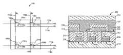
- FIG. 1is a diagram illustrating one embodiment of an array of phase change memory cells.
- FIG. 2Aillustrates a cross-sectional view of one embodiment of an array of phase change memory cells.
- FIG. 2Billustrates a perpendicular cross-sectional view of the array of phase change memory cells illustrated in FIG. 2A .
- FIG. 2Cillustrates a top view of the array of phase change memory cells illustrated in FIG. 2A .
- FIG. 3Aillustrates a cross-sectional view of one embodiment of a preprocessed wafer.
- FIG. 3Billustrates a perpendicular cross-sectional view of the preprocessed wafer illustrated in FIG. 3A .
- FIG. 3Cillustrates a top view of the preprocessed wafer illustrated in FIG. 3A .
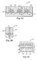
- FIG. 4illustrates a cross-sectional view of one embodiment of the preprocessed wafer, a conductive material layer, and a first dielectric material layer.
- FIG. 5illustrates a cross-sectional view of one embodiment of the preprocessed wafer, ground lines, and first dielectric material layer after etching.
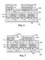
- FIG. 6illustrates a cross-sectional view of one embodiment of the preprocessed wafer, ground lines, first dielectric material layer, and a second dielectric material layer.
- FIG. 7illustrates a cross-sectional view of one embodiment of the preprocessed wafer, ground lines, first dielectric material layer, and sidewall spacers after etching.
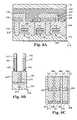
- FIG. 8Aillustrates a cross-sectional view of one embodiment of the preprocessed wafer, encapsulated ground lines, a phase change material layer, and an electrode material layer.
- FIG. 8Billustrates a perpendicular cross-sectional view of the wafer illustrated in FIG. 8A .
- FIG. 9Aillustrates a cross-sectional view of one embodiment of the preprocessed wafer, encapsulated ground lines, phase change material layer, and bit lines after etching.
- FIG. 9Billustrates a perpendicular cross-sectional view of the wafer illustrated in FIG. 9A .
- FIG. 9Cillustrates a top view of the wafer illustrated in FIG. 9A .
- FIG. 10Aillustrates a cross-sectional view of one embodiment of a preprocessed wafer.
- FIG. 10Billustrates a perpendicular cross-sectional view of the preprocessed wafer illustrated in FIG. 10A .
- FIG. 10Cillustrates a top view of the preprocessed wafer illustrated in FIG. 10A .
- FIG. 12illustrates a cross-sectional view of one embodiment of the preprocessed wafer, ground lines, and first dielectric material layer after etching.
- FIG. 13illustrates a cross-sectional view of one embodiment of the preprocessed wafer, ground lines, first dielectric material layer, and a second dielectric material layer.
- FIG. 14illustrates a cross-sectional view of one embodiment of the preprocessed wafer, ground lines, first dielectric material layer, and sidewall spacers after etching.
- FIG. 15Billustrates a perpendicular cross-sectional view of the wafer illustrated in FIG. 15A .
- FIG. 16Aillustrates a cross-sectional view of one embodiment of the preprocessed wafer, encapsulated ground lines, dielectric material layer, and a phase change material layer.
- FIG. 17Billustrates a perpendicular cross-sectional view of the wafer illustrated in FIG. 17A .
- FIG. 1is a diagram illustrating one embodiment of an array of phase-change memory cells 100 .
- Memory array 100is fabricated using line lithography and self-aligned processing to minimize critical lithography steps.
- the interface resistance between metal and active materialis overlay-insensitive and by maximizing the interface areas, parasitic resistances are minimized.
- Memory array 100does not have any isolated, small patterns such that the chemical mechanical planarization (CMP) process window is improved and mechanical stability is improved.
- CMPchemical mechanical planarization
- Phase-change memory cell 104 cis electrically coupled to bit line 112 b , word line 110 a , and ground line 114 a
- phase-change memory cell 104 dis electrically coupled to bit line 112 b , word line 110 b , and ground line 114 b.
- Each phase-change memory cell 104includes a phase-change element 106 and a transistor 108 . While transistor 108 is a field-effect transistor (FET) in the illustrated embodiment, in other embodiments, transistor 108 can be another suitable device such as a bipolar transistor or a 3D transistor structure.
- Phase-change memory cell 104 aincludes phase-change element 106 a and transistor 108 a . One side of phase-change element 106 a is electrically coupled to bit line 112 a , and the other side of phase-change element 106 a is electrically coupled to one side of the source-drain path of transistor 108 a . The other side of the source-drain path of transistor 108 a is electrically coupled to ground line 114 a .
- phase-change memory cell 104 bincludes phase-change element 106 b and transistor 108 b .
- One side of phase-change element 106 bis electrically coupled to bit line 112 a
- the other side of phase-change element 106 bis electrically coupled to one side of the source-drain path of transistor 108 b .
- the other side of the source-drain path of transistor 108 bis electrically coupled to ground line 114 b .
- the gate of transistor 108 bis electrically coupled to word line 110 b.
- Phase-change memory cell 104 cincludes phase-change element 106 c and transistor 108 c .
- One side of phase-change element 106 cis electrically coupled to bit line 112 b and the other side of phase-change element 106 c is electrically coupled to one side of the source-drain path of transistor 108 c .
- the other side of the source-drain path of transistor 108 cis electrically coupled to ground line 114 a .
- the gate of transistor 108 cis electrically coupled to word line 110 a .
- Phase-change memory cell 104 dincludes phase-change element 106 d and transistor 108 d .
- phase-change element 106 dis electrically coupled to bit line 112 b and the other side of phase-change element 106 d is electrically coupled to one side of the source-drain path of transistor 108 d .
- the other side of the source-drain path of transistor 108 dis electrically coupled to ground line 114 b .
- the gate of transistor 108 dis electrically coupled to word line 110 b.
- each phase-change element 106is electrically coupled to a ground line 114 and each transistor 108 is electrically coupled to a bit line 112 .
- phase-change memory cell 104 aone side of phase-change element 106 a is electrically coupled to ground line 114 a .
- the other side of phase-change element 106 ais electrically coupled to one side of the source-drain path of transistor 108 a .
- the other side of the source-drain path of transistor 108 ais electrically coupled to bit line 112 a .
- the ground lines 114have a lower potential than the bit lines 112 .
- Each phase-change element 106comprises a phase-change material that may be made up of a variety of materials in accordance with the present invention.
- chalcogenide alloysthat contain one or more elements from group VI of the periodic table are useful as such materials.
- the phase-change material of phase-change element 106is made up of a chalcogenide compound material, such as GeSbTe, SbTe, GeTe or AgInSbTe.
- the phase-change materialis chalcogen free, such as GeSb, GaSb, InSb, or GeGaInSb.
- the phase-change materialis made up of any suitable material including one or more of the elements Ge, Sb, Te, Ga, As, In, Se, and S.
- phase-change memory cell 104 aDuring a set operation of phase-change memory cell 104 a , a set current or voltage pulse is selectively enabled and sent through bit line 112 a to phase-change element 106 a thereby heating it above it's crystallization temperature (but usually below it's melting temperature) with word line 110 a selected to activate transistor 108 a . In this way, phase-change element 106 a reaches its crystalline state during this set operation.
- a reset current or voltage pulseis selectively enabled to bit line 112 a and sent to phase-change material element 106 a . The reset current or voltage quickly heats phase-change element 106 a above its melting temperature.
- FIG. 2Aillustrates a cross-sectional view of one embodiment of an array of phase change memory cells 200 .
- FIG. 2Billustrates a perpendicular cross-sectional view of array of phase change memory cells 200 illustrated in FIG. 2A .
- FIG. 2Cillustrates a top view of array of phase change memory cells 200 illustrated in FIG. 2A .
- array of phase change memory cells 100is similar to array of phase change memory cells 200 .
- Array of phase change memory cells 200includes substrate 212 , transistors 108 , word lines 110 , first contacts 206 , second contacts 208 , ground lines 114 , dielectric material 210 , 216 , and 230 , shallow trench isolation (STI) 214 , inter level dielectric (ILD) 215 , phase change material 107 , and bits lines 112 .
- Metal wiring(not shown) follows after the bit line level.
- Transistors 108 for selecting storage locations 105 in phase change material 107are formed in substrate 212 in rows and columns. The gates of transistors 108 are electrically coupled to word lines 110 . Dielectric material 210 is deposited over transistors 108 and word lines 110 . First contacts 206 electrically couple one side of the source-drain path of each transistor 108 to a ground line 114 . Second contacts 208 electrically couple the other side of the source-drain path of each transistor 108 to a storage location 105 , which is a part of phase change material 107 . Each line of phase change material 107 is electrically coupled to a bit line 112 . Bit lines 112 are perpendicular to word lines 110 and ground lines 114 .
- Dielectric material 230insulates ground lines 114 above first contacts 206 .
- Dielectric material 216insulates bits lines 112 and lines of phase change material 107 from adjacent bit lines 112 and lines of phase change material 107 .
- STI 214insulates transistors 108 from adjacent transistors 108
- ILD 215insulates second contacts 208 from adjacent second contacts 208 .
- Lines of phase change material 107which include storage locations 105 , are self-aligned to bit lines 112 .
- the self-alignmentminimizes critical lithography steps in the fabrication of array of phase change memory cells 200 .
- the interface resistances between second contacts 208 and phase change material 107 and between phase change material 107 and bit lines 112is overlay insensitive and parasitic resistances are minimized.
- array of phase change memory cells 200is scalable to 8F 2 for dual gate memory cells, where “F” is the minimum feature size, or to 6F 2 for single gate memory cells.
- Fis the minimum feature size
- 6F 2for single gate memory cells.
- an active gate of a transistor 108 between every two adjacent memory cellsis replaced with an isolation gate (i.e., the transistor is not used as a switch; rather it is always turned off), and a dummy ground line is formed above the isolation gate to separate adjacent memory cells.
- FIGS. 3A-9CA first embodiment of a method for fabricating array of phase change memory cells 200 is described and illustrated with reference to the following FIGS. 3A-9C .
- a second embodiment of a method for fabricating array of phase change memory cells 200is described and illustrated with reference to the following FIGS. 10A-17C .
- FIG. 3Aillustrates a cross-sectional view of one embodiment of a preprocessed wafer 218 .
- FIG. 3Billustrates a perpendicular cross-sectional view of preprocessed wafer 218 illustrated in FIG. 3A .
- FIG. 3Cillustrates a top view of preprocessed wafer 218 illustrated in FIG. 3A .
- Preprocessed wafer 218includes substrate 212 , transistors 108 , word lines 110 , first contacts 206 , second contacts 208 , STI 214 , ILD 215 , and dielectric material 210 .
- Transistors 108are formed in substrate 212 in rows and columns. The gates of transistors 108 are electrically coupled to word lines 110 . Dielectric material 210 is deposited over transistors 108 and word lines 110 . First contacts 206 are electrically coupled to one side of the source-drain path of each transistor 108 . Second contacts 208 are electrically coupled to the other side of the source-drain path of each transistor 108 .
- STI 214insulates transistors 108 from adjacent transistors 108
- ILD 215insulates second contacts 208 from adjacent second contacts 208 .
- First contacts 206 and second contacts 208are contact plugs, such as W plugs, Cu plugs, or other suitable conducting material plugs.
- Word lines 110comprise doped poly-Si, W, TiN, NiSi, CoSi, TiSi, WSi X , or another suitable material.
- Dielectric material 210comprises SiN or other suitable material that enables a borderless contact formation process for first contacts 206 and second contacts 208 .
- STI 214 and ILD 215comprise SiO 2 , fluorinated silica glass (FSG), boro-phosphorous silicate glass (BPSG), boro-silicate glass (BSG), or other suitable dielectric material.
- Word lines 110are perpendicular to STI 214 and ILD 215 .
- FIG. 4illustrates a cross-sectional view of one embodiment of preprocessed wafer 218 , a conductive material layer 114 a , and a first dielectric material layer 230 a .
- Conductive materialsuch as W, Al, Cu, or other suitable conductive material is deposited over preprocessed wafer 218 to provide conductive material layer 114 a .
- Conductive material layer 114 ais deposited using chemical vapor deposition (CVD), atomic layer deposition (ALD), metal organic chemical vapor deposition (MOCVD), plasma vapor deposition (PVD), jet vapor deposition (JVP), or other suitable deposition technique.
- CVDchemical vapor deposition
- ALDatomic layer deposition
- MOCVDmetal organic chemical vapor deposition
- PVDplasma vapor deposition
- JVPjet vapor deposition
- Dielectric materialsuch as SiN or other suitable dielectric material, is deposited over conductive material layer 114 a to provide first dielectric material layer 230 a .
- First dielectric material layer 230 ais deposited using CVD, ALD, MOCVD, PVD, JVP, high-density plasma (HDP), or other suitable deposition technique.
- FIG. 5illustrates a cross-sectional view of one embodiment of preprocessed wafer 218 , ground lines 114 , and first dielectric material layer 230 b after etching first dielectric material layer 230 a and conductive material layer 114 a .
- First dielectric material layer 230 a and conductive material layer 114 aare etched to provide first dielectric material layer 230 b and ground lines 114 and to form trenches 220 .
- Line lithographyis used to pattern trenches 220 having a width 221 to expose second contacts 208 .
- the line lithographydoes not need to be precisely centered over second contacts 208 as long as second contacts 208 are exposed. In this way, the line lithography is less critical yet the desired memory cell size is obtained.
- FIG. 6illustrates a cross-sectional view of one embodiment of preprocessed wafer 218 , ground lines 114 , first dielectric material layer 230 b , and a second dielectric material layer 230 c .
- Dielectric materialsuch as SiN or other suitable dielectric material, is conformally deposited over exposed portions of first dielectric material layer 230 b , ground lines 114 , and preprocessed wafer 218 to provide second dielectric material layer 230 c .
- Second dielectric material layer 230 cis deposited using CVD, ALD, MOCVD, PVD, JVP, HDP, or other suitable deposition technique.
- FIG. 7illustrates a cross-sectional view of one embodiment of preprocessed wafer 218 , ground lines 114 , first dielectric material layer 230 b , and sidewall spacers 230 d after etching second dielectric material layer 230 c .
- Second dielectric material layer 230 cis etched using a spacer etch to form sidewall spacers 230 d and to expose second contacts 208 .
- First dielectric material layer 230 b and sidewall spacers 230 dare collectively referred to as dielectric material 230 .
- FIG. 8Aillustrates a cross-sectional view of one embodiment of preprocessed wafer 218 , ground lines 114 encapsulated by dielectric material 230 , a phase change material layer 107 a , and an electrode material layer 113 a .
- FIG. 8Billustrates a perpendicular cross-sectional view of the wafer illustrated in FIG. 8A .
- Phase change materialsuch as a chalcogenide compound material or other suitable phase change material, is deposited over exposed portions of dielectric material 230 and preprocessed wafer 218 to provide phase change material layer 107 a .
- Phase change material layer 107 ais deposited using CVD, ALD, MOCVD, PVD, JVP, or other suitable deposition technique. In one embodiment, phase change material layer 107 a is planarized to expose dielectric material 230 .
- Electrode materialsuch as TiN, TaN, W, Al, Cu, TiSiN, TaSiN, or other suitable electrode material, is deposited over phase change material layer 107 a to provide electrode material layer 113 a .
- Electrode material layer 113 ais deposited using CVD, ALD, MOCVD, PVD, JVP, or other suitable deposition technique.
- FIG. 9Aillustrates a cross-sectional view of one embodiment of preprocessed wafer 218 , ground lines 114 encapsulated by dielectric material 230 , phase change material layer 107 , and bit lines 112 after etching electrode material layer 113 a and phase change material layer 107 a .
- FIG. 9Billustrates a perpendicular cross-sectional view of the wafer illustrated in FIG. 9A
- FIG. 9Cillustrates a top view of the wafer illustrated in FIG. 9A .
- Electrode material layer 113 a and phase change material layer 107 aare etched to provide bit lines 112 and phase change material layer 107 , which is self-aligned to bit lines 112 .
- phase change material layer 107 ais planarized to expose dielectric material 230
- electrode material layer 113 a and phase change material layer 107 aare etched to provide bit lines 112 and phase change elements 106 , which are self-aligned to bit lines 112 .
- phase change material layer 107is optionally undercut etched.
- Line lithographyis used to pattern bit lines 112 and lines of phase change material 107 perpendicular to trenches 220 such that each storage location 105 in phase change material 107 contacts a second contact 208 .
- the line lithographydoes not need to be precisely centered over second contacts 208 as long as the bottom portion of each storage location 105 in phase change material 107 contacts a second contact 208 . In this way, the line lithography is less critical yet the desired memory cell size is obtained.
- Dielectric materialsuch as SiO 2 , FSG, BPSG, BSG, or other suitable dielectric material, is deposited over exposed portions of bit lines 112 , phase change material layer 107 , dielectric material layer 230 , and preprocessed wafer 218 .
- the dielectric material layeris deposited using CVD, ALD, MOCVD, PVD, JVP, HDP, or other suitable deposition technique.
- the dielectric material layeris planarized to expose bit lines 112 and provide dielectric material layer 216 .
- the dielectric material layeris planarized using CMP or another suitable planarization technique to provide array of phase change memory cells 200 a illustrated in FIGS. 2A-2C .
- FIG. 10Aillustrates a cross-sectional view of one embodiment of a preprocessed wafer 218 .
- FIG. 10Billustrates a perpendicular cross-sectional view of preprocessed wafer 218 illustrated in FIG. 10A .
- FIG. 10Cillustrates a top view of preprocessed wafer 218 illustrated in FIG. 10A .
- Preprocessed wafer 218includes substrate 212 , transistors 108 , word lines 110 , first contacts 206 , second contacts 208 , STI 214 , ILD 215 , and dielectric material 210 .
- Transistors 108are formed in substrate 212 in rows and columns. The gates of transistors 108 are electrically coupled to word lines 110 . Dielectric material 210 is deposited over transistors 108 and word lines 110 . First contacts 206 are electrically coupled to one side of the source-drain path of each transistor 108 . Second contacts 208 are electrically coupled to the other side of the source-drain path of each transistor 108 .
- STI 214insulates transistors 108 from adjacent transistors 108
- ILD 215insulates second contacts 208 from adjacent second contacts 208 .
- First contacts 206 and second contacts 208are contact plugs, such as W plugs, Cu plugs, or other suitable conducting material plugs.
- Word lines 110comprise doped poly-Si, W, TiN, NiSi, CoSi, TiSi, WSi X , or another suitable material.
- Dielectric material 210comprises SiN or other suitable material that enables a borderless contact formation process for first contacts 206 and second contacts 208 .
- STI 214 and ILD 215comprise SiO 2 , FSG, BPSG, BSG, or other suitable dielectric material.
- Word lines 110are perpendicular to STI 214 and ILD 215 .
- FIG. 11illustrates a cross-sectional view of one embodiment of preprocessed wafer 218 , a conductive material layer 114 a , and a first dielectric material layer 230 a .
- Conductive materialsuch as W, Al, Cu, or other suitable conductive material is deposited over preprocessed wafer 218 to provide conductive material layer 114 a .
- Conductive material layer 114 ais deposited using CVD, ALD, MOCVD, PVD, JVP, or other suitable deposition technique.
- Dielectric materialsuch as SiN or other suitable dielectric material, is deposited over conductive material layer 114 a to provide first dielectric material layer 230 a .
- First dielectric material layer 230 ais deposited using CVD, ALD, MOCVD, PVD, JVP, HDP, or other suitable deposition technique.
- FIG. 12illustrates a cross-sectional view of one embodiment of preprocessed wafer 218 , ground lines 114 , and first dielectric material layer 230 b after etching first dielectric material layer 230 a and conductive material layer 114 a .
- First dielectric material layer 230 a and conductive material layer 114 aare etched to provide first dielectric material layer 230 b and ground lines 114 and to form trenches 220 .
- Line lithographyis used to pattern trenches 220 having a width 221 to expose second contacts 208 .
- the line lithographydoes not need to be precisely centered over second contacts 208 as long as second contacts 208 are exposed. In this way, the line lithography is less critical yet the desired memory cell size is obtained.
- FIG. 13illustrates a cross-sectional view of one embodiment of preprocessed wafer 218 , ground lines 114 , first dielectric material layer 230 b , and a second dielectric material layer 230 c .
- Dielectric materialsuch as SiN or other suitable dielectric material, is conformally deposited over exposed portions of first dielectric material layer 230 b , ground lines 114 , and preprocessed wafer 218 to provide second dielectric material layer 230 c .
- Second dielectric material layer 230 cis deposited using CVD, ALD, MOCVD, PVD, JVP, HDP, or other suitable deposition technique.
- FIG. 15Aillustrates a cross-sectional view of one embodiment of preprocessed wafer 218 , ground lines 114 encapsulated by dielectric material 230 , and a dielectric material layer 216 a .
- FIG. 15Billustrates a perpendicular cross-sectional view of the wafer illustrated in FIG. 15A .
- Dielectric materialsuch as SiO 2 , FSG, BPSG, BSG, or other suitable dielectric material, is deposited over exposed portions of dielectric material 230 and preprocessed wafer 218 to provide dielectric material layer 216 a .
- Dielectric material layer 216 ais deposited using CVD, ALD, MOCVD, PVD, JVP, HDP, or other suitable deposition technique.
- Phase change materialsuch as a chalcogenide compound material or other suitable phase change material
- phase change material layeris deposited over exposed portions of dielectric material layer 216 , dielectric material 230 , and preprocessed wafer 218 to provide a phase change material layer.
- the phase change material layeris deposited using CVD, ALD, MOCVD, PVD, JVP, or other suitable deposition technique.
- the phase change material layeris planarized to expose dielectric material layer 216 to provide phase change material layer 107 a .
- the phase change material layeris planarized using CMP or another suitable planarization technique.
- FIG. 17Aillustrates a cross-sectional view of one embodiment of preprocessed wafer 218 , ground lines 114 encapsulated by dielectric material 230 , phase change material layer 107 , and bit lines 112 .
- FIG. 17Billustrates a perpendicular cross-sectional view of the wafer illustrated in FIG. 17A
- FIG. 17Cillustrates a top view of the wafer illustrated in FIG. 17A .
- Phase change material layer 107 ais recess etched to provide phase change material layer 107 .
- Electrode materialsuch as TiN, TaN, W, Al, Cu, TiSiN, TaSiN, or other suitable electrode material, is deposited over phase change material layer 107 and dielectric material layer 216 to provide an electrode material layer.
- the electrode material layeris deposited using CVD, ALD, MOCVD, PVD, JVP, or other suitable deposition technique.
- the electrode material layeris planarized to expose dielectric material layer 216 to provide bit lines 112 .
- the electrode material layeris planarized using CMP or another suitable planarization technique to provide array of phase change memory cells 200 a illustrated in FIGS. 2A-2C .
Landscapes
- Chemical & Material Sciences (AREA)
- Crystallography & Structural Chemistry (AREA)
- Engineering & Computer Science (AREA)
- Computer Hardware Design (AREA)
- Manufacturing & Machinery (AREA)
- Semiconductor Memories (AREA)
- Non-Volatile Memory (AREA)
Abstract
Description
Claims (22)
Priority Applications (5)
| Application Number | Priority Date | Filing Date | Title |
|---|---|---|---|
| US11/366,151US7362608B2 (en) | 2006-03-02 | 2006-03-02 | Phase change memory fabricated using self-aligned processing |
| EP07004166AEP1830362A3 (en) | 2006-03-02 | 2007-02-28 | Phase change memory fabricated using self-aligned processing |
| JP2007051384AJP2007273962A (en) | 2006-03-02 | 2007-03-01 | Phase change memory formed using a self-aligned process |
| CN2007101006984ACN101064331B (en) | 2006-03-02 | 2007-03-02 | Phase-change memory fabricated by self-aligned process |
| KR1020070020883AKR100807677B1 (en) | 2006-03-02 | 2007-03-02 | Phase change memory fabricated using self-aligned processing |
Applications Claiming Priority (1)
| Application Number | Priority Date | Filing Date | Title |
|---|---|---|---|
| US11/366,151US7362608B2 (en) | 2006-03-02 | 2006-03-02 | Phase change memory fabricated using self-aligned processing |
Publications (2)
| Publication Number | Publication Date |
|---|---|
| US20070206408A1 US20070206408A1 (en) | 2007-09-06 |
| US7362608B2true US7362608B2 (en) | 2008-04-22 |
Family
ID=38080813
Family Applications (1)
| Application Number | Title | Priority Date | Filing Date |
|---|---|---|---|
| US11/366,151Expired - Fee RelatedUS7362608B2 (en) | 2006-03-02 | 2006-03-02 | Phase change memory fabricated using self-aligned processing |
Country Status (5)
| Country | Link |
|---|---|
| US (1) | US7362608B2 (en) |
| EP (1) | EP1830362A3 (en) |
| JP (1) | JP2007273962A (en) |
| KR (1) | KR100807677B1 (en) |
| CN (1) | CN101064331B (en) |
Cited By (9)
| Publication number | Priority date | Publication date | Assignee | Title |
|---|---|---|---|---|
| US20080056022A1 (en)* | 2006-08-31 | 2008-03-06 | Micron Technology, Inc. | Phase-Change Random Access Memory Employing Read Before Write for Resistance Stabilization |
| US7889536B2 (en)* | 2007-12-17 | 2011-02-15 | Qimonda Ag | Integrated circuit including quench devices |
| US20110049462A1 (en)* | 2009-08-28 | 2011-03-03 | International Business Machines Corporation | Flat lower bottom electrode for phase change memory cell |
| US20110049460A1 (en)* | 2009-08-28 | 2011-03-03 | International Business Machines Corporation | Single mask adder phase change memory element |
| US20110116307A1 (en)* | 2009-11-16 | 2011-05-19 | International Business Machines Corporation | Phase change memory device suitable for high temperature operation |
| US20110121252A1 (en)* | 2009-11-25 | 2011-05-26 | International Business Machines Corporation | Single mask adder phase change memory element |
| US20110210307A1 (en)* | 2009-08-28 | 2011-09-01 | International Business Machines Corporation | Chemical mechanical polishing stop layer for fully amorphous phase change memory pore cell |
| US20120075923A1 (en)* | 2010-09-23 | 2012-03-29 | Numonyx B.V. | Phase change memory state determination using threshold edge detection |
| US9059394B2 (en) | 2009-11-16 | 2015-06-16 | International Business Machines Corporation | Self-aligned lower bottom electrode |
Families Citing this family (172)
| Publication number | Priority date | Publication date | Assignee | Title |
|---|---|---|---|---|
| EP2244293A4 (en)* | 2008-02-12 | 2011-08-10 | Panasonic Corp | NON-VOLATILE SEMICONDUCTOR MEMORY DEVICE AND METHOD FOR MANUFACTURING THE SAME |
| WO2009111256A2 (en)* | 2008-03-04 | 2009-09-11 | Arizona Board Regents For And On Behalf Of Arizona State University | Method and system for surface water treatment |
| US10388863B2 (en) | 2009-10-12 | 2019-08-20 | Monolithic 3D Inc. | 3D memory device and structure |
| US10157909B2 (en) | 2009-10-12 | 2018-12-18 | Monolithic 3D Inc. | 3D semiconductor device and structure |
| US10910364B2 (en) | 2009-10-12 | 2021-02-02 | Monolitaic 3D Inc. | 3D semiconductor device |
| US10043781B2 (en) | 2009-10-12 | 2018-08-07 | Monolithic 3D Inc. | 3D semiconductor device and structure |
| US10366970B2 (en) | 2009-10-12 | 2019-07-30 | Monolithic 3D Inc. | 3D semiconductor device and structure |
| US11374118B2 (en) | 2009-10-12 | 2022-06-28 | Monolithic 3D Inc. | Method to form a 3D integrated circuit |
| US12027518B1 (en) | 2009-10-12 | 2024-07-02 | Monolithic 3D Inc. | 3D semiconductor devices and structures with metal layers |
| US11984445B2 (en) | 2009-10-12 | 2024-05-14 | Monolithic 3D Inc. | 3D semiconductor devices and structures with metal layers |
| US9941332B2 (en)* | 2009-10-12 | 2018-04-10 | Monolithic 3D Inc. | Semiconductor memory device and structure |
| US10354995B2 (en) | 2009-10-12 | 2019-07-16 | Monolithic 3D Inc. | Semiconductor memory device and structure |
| US11018133B2 (en) | 2009-10-12 | 2021-05-25 | Monolithic 3D Inc. | 3D integrated circuit |
| US10217667B2 (en) | 2011-06-28 | 2019-02-26 | Monolithic 3D Inc. | 3D semiconductor device, fabrication method and system |
| US12362219B2 (en) | 2010-11-18 | 2025-07-15 | Monolithic 3D Inc. | 3D semiconductor memory device and structure |
| US11482440B2 (en) | 2010-12-16 | 2022-10-25 | Monolithic 3D Inc. | 3D semiconductor device and structure with a built-in test circuit for repairing faulty circuits |
| US10497713B2 (en) | 2010-11-18 | 2019-12-03 | Monolithic 3D Inc. | 3D semiconductor memory device and structure |
| US11469271B2 (en) | 2010-10-11 | 2022-10-11 | Monolithic 3D Inc. | Method to produce 3D semiconductor devices and structures with memory |
| US11315980B1 (en) | 2010-10-11 | 2022-04-26 | Monolithic 3D Inc. | 3D semiconductor device and structure with transistors |
| US11024673B1 (en) | 2010-10-11 | 2021-06-01 | Monolithic 3D Inc. | 3D semiconductor device and structure |
| US11227897B2 (en) | 2010-10-11 | 2022-01-18 | Monolithic 3D Inc. | Method for producing a 3D semiconductor memory device and structure |
| US10896931B1 (en) | 2010-10-11 | 2021-01-19 | Monolithic 3D Inc. | 3D semiconductor device and structure |
| US10290682B2 (en) | 2010-10-11 | 2019-05-14 | Monolithic 3D Inc. | 3D IC semiconductor device and structure with stacked memory |
| US11018191B1 (en) | 2010-10-11 | 2021-05-25 | Monolithic 3D Inc. | 3D semiconductor device and structure |
| US11257867B1 (en) | 2010-10-11 | 2022-02-22 | Monolithic 3D Inc. | 3D semiconductor device and structure with oxide bonds |
| US11600667B1 (en) | 2010-10-11 | 2023-03-07 | Monolithic 3D Inc. | Method to produce 3D semiconductor devices and structures with memory |
| US11158674B2 (en) | 2010-10-11 | 2021-10-26 | Monolithic 3D Inc. | Method to produce a 3D semiconductor device and structure |
| US11164898B2 (en) | 2010-10-13 | 2021-11-02 | Monolithic 3D Inc. | Multilevel semiconductor device and structure |
| US11133344B2 (en) | 2010-10-13 | 2021-09-28 | Monolithic 3D Inc. | Multilevel semiconductor device and structure with image sensors |
| US11063071B1 (en) | 2010-10-13 | 2021-07-13 | Monolithic 3D Inc. | Multilevel semiconductor device and structure with waveguides |
| US11694922B2 (en) | 2010-10-13 | 2023-07-04 | Monolithic 3D Inc. | Multilevel semiconductor device and structure with oxide bonding |
| US10943934B2 (en) | 2010-10-13 | 2021-03-09 | Monolithic 3D Inc. | Multilevel semiconductor device and structure |
| US11605663B2 (en) | 2010-10-13 | 2023-03-14 | Monolithic 3D Inc. | Multilevel semiconductor device and structure with image sensors and wafer bonding |
| US10978501B1 (en) | 2010-10-13 | 2021-04-13 | Monolithic 3D Inc. | Multilevel semiconductor device and structure with waveguides |
| US10998374B1 (en) | 2010-10-13 | 2021-05-04 | Monolithic 3D Inc. | Multilevel semiconductor device and structure |
| US11855100B2 (en) | 2010-10-13 | 2023-12-26 | Monolithic 3D Inc. | Multilevel semiconductor device and structure with oxide bonding |
| US12360310B2 (en) | 2010-10-13 | 2025-07-15 | Monolithic 3D Inc. | Multilevel semiconductor device and structure with oxide bonding |
| US11437368B2 (en) | 2010-10-13 | 2022-09-06 | Monolithic 3D Inc. | Multilevel semiconductor device and structure with oxide bonding |
| US11869915B2 (en) | 2010-10-13 | 2024-01-09 | Monolithic 3D Inc. | Multilevel semiconductor device and structure with image sensors and wafer bonding |
| US11404466B2 (en) | 2010-10-13 | 2022-08-02 | Monolithic 3D Inc. | Multilevel semiconductor device and structure with image sensors |
| US10679977B2 (en) | 2010-10-13 | 2020-06-09 | Monolithic 3D Inc. | 3D microdisplay device and structure |
| US11855114B2 (en) | 2010-10-13 | 2023-12-26 | Monolithic 3D Inc. | Multilevel semiconductor device and structure with image sensors and wafer bonding |
| US12080743B2 (en) | 2010-10-13 | 2024-09-03 | Monolithic 3D Inc. | Multilevel semiconductor device and structure with image sensors and wafer bonding |
| US11043523B1 (en) | 2010-10-13 | 2021-06-22 | Monolithic 3D Inc. | Multilevel semiconductor device and structure with image sensors |
| US12094892B2 (en) | 2010-10-13 | 2024-09-17 | Monolithic 3D Inc. | 3D micro display device and structure |
| US10833108B2 (en) | 2010-10-13 | 2020-11-10 | Monolithic 3D Inc. | 3D microdisplay device and structure |
| US11163112B2 (en) | 2010-10-13 | 2021-11-02 | Monolithic 3D Inc. | Multilevel semiconductor device and structure with electromagnetic modulators |
| US11929372B2 (en) | 2010-10-13 | 2024-03-12 | Monolithic 3D Inc. | Multilevel semiconductor device and structure with image sensors and wafer bonding |
| US11984438B2 (en) | 2010-10-13 | 2024-05-14 | Monolithic 3D Inc. | Multilevel semiconductor device and structure with oxide bonding |
| US11327227B2 (en) | 2010-10-13 | 2022-05-10 | Monolithic 3D Inc. | Multilevel semiconductor device and structure with electromagnetic modulators |
| US11443971B2 (en) | 2010-11-18 | 2022-09-13 | Monolithic 3D Inc. | 3D semiconductor device and structure with memory |
| US12154817B1 (en) | 2010-11-18 | 2024-11-26 | Monolithic 3D Inc. | Methods for producing a 3D semiconductor memory device and structure |
| US11004719B1 (en) | 2010-11-18 | 2021-05-11 | Monolithic 3D Inc. | Methods for producing a 3D semiconductor memory device and structure |
| US11107721B2 (en) | 2010-11-18 | 2021-08-31 | Monolithic 3D Inc. | 3D semiconductor device and structure with NAND logic |
| US11482439B2 (en) | 2010-11-18 | 2022-10-25 | Monolithic 3D Inc. | Methods for producing a 3D semiconductor memory device comprising charge trap junction-less transistors |
| US11211279B2 (en) | 2010-11-18 | 2021-12-28 | Monolithic 3D Inc. | Method for processing a 3D integrated circuit and structure |
| US12068187B2 (en) | 2010-11-18 | 2024-08-20 | Monolithic 3D Inc. | 3D semiconductor device and structure with bonding and DRAM memory cells |
| US11031275B2 (en) | 2010-11-18 | 2021-06-08 | Monolithic 3D Inc. | 3D semiconductor device and structure with memory |
| US12136562B2 (en) | 2010-11-18 | 2024-11-05 | Monolithic 3D Inc. | 3D semiconductor device and structure with single-crystal layers |
| US11854857B1 (en) | 2010-11-18 | 2023-12-26 | Monolithic 3D Inc. | Methods for producing a 3D semiconductor device and structure with memory cells and multiple metal layers |
| US11355381B2 (en) | 2010-11-18 | 2022-06-07 | Monolithic 3D Inc. | 3D semiconductor memory device and structure |
| US12100611B2 (en) | 2010-11-18 | 2024-09-24 | Monolithic 3D Inc. | Methods for producing a 3D semiconductor device and structure with memory cells and multiple metal layers |
| US12243765B2 (en) | 2010-11-18 | 2025-03-04 | Monolithic 3D Inc. | 3D semiconductor device and structure with metal layers and memory cells |
| US11862503B2 (en) | 2010-11-18 | 2024-01-02 | Monolithic 3D Inc. | Method for producing a 3D semiconductor device and structure with memory cells and multiple metal layers |
| US11355380B2 (en) | 2010-11-18 | 2022-06-07 | Monolithic 3D Inc. | Methods for producing 3D semiconductor memory device and structure utilizing alignment marks |
| US11121021B2 (en) | 2010-11-18 | 2021-09-14 | Monolithic 3D Inc. | 3D semiconductor device and structure |
| US11569117B2 (en) | 2010-11-18 | 2023-01-31 | Monolithic 3D Inc. | 3D semiconductor device and structure with single-crystal layers |
| US11804396B2 (en) | 2010-11-18 | 2023-10-31 | Monolithic 3D Inc. | Methods for producing a 3D semiconductor device and structure with memory cells and multiple metal layers |
| US12144190B2 (en) | 2010-11-18 | 2024-11-12 | Monolithic 3D Inc. | 3D semiconductor device and structure with bonding and memory cells preliminary class |
| US11923230B1 (en) | 2010-11-18 | 2024-03-05 | Monolithic 3D Inc. | 3D semiconductor device and structure with bonding |
| US11495484B2 (en) | 2010-11-18 | 2022-11-08 | Monolithic 3D Inc. | 3D semiconductor devices and structures with at least two single-crystal layers |
| US11901210B2 (en) | 2010-11-18 | 2024-02-13 | Monolithic 3D Inc. | 3D semiconductor device and structure with memory |
| US11610802B2 (en) | 2010-11-18 | 2023-03-21 | Monolithic 3D Inc. | Method for producing a 3D semiconductor device and structure with single crystal transistors and metal gate electrodes |
| US11615977B2 (en) | 2010-11-18 | 2023-03-28 | Monolithic 3D Inc. | 3D semiconductor memory device and structure |
| US11735462B2 (en) | 2010-11-18 | 2023-08-22 | Monolithic 3D Inc. | 3D semiconductor device and structure with single-crystal layers |
| US11784082B2 (en) | 2010-11-18 | 2023-10-10 | Monolithic 3D Inc. | 3D semiconductor device and structure with bonding |
| US11482438B2 (en) | 2010-11-18 | 2022-10-25 | Monolithic 3D Inc. | Methods for producing a 3D semiconductor memory device and structure |
| US12272586B2 (en) | 2010-11-18 | 2025-04-08 | Monolithic 3D Inc. | 3D semiconductor memory device and structure with memory and metal layers |
| US12125737B1 (en) | 2010-11-18 | 2024-10-22 | Monolithic 3D Inc. | 3D semiconductor device and structure with metal layers and memory cells |
| US11164770B1 (en) | 2010-11-18 | 2021-11-02 | Monolithic 3D Inc. | Method for producing a 3D semiconductor memory device and structure |
| US11521888B2 (en) | 2010-11-18 | 2022-12-06 | Monolithic 3D Inc. | 3D semiconductor device and structure with high-k metal gate transistors |
| US11018042B1 (en) | 2010-11-18 | 2021-05-25 | Monolithic 3D Inc. | 3D semiconductor memory device and structure |
| US11094576B1 (en) | 2010-11-18 | 2021-08-17 | Monolithic 3D Inc. | Methods for producing a 3D semiconductor memory device and structure |
| US11508605B2 (en) | 2010-11-18 | 2022-11-22 | Monolithic 3D Inc. | 3D semiconductor memory device and structure |
| US12033884B2 (en) | 2010-11-18 | 2024-07-09 | Monolithic 3D Inc. | Methods for producing a 3D semiconductor device and structure with memory cells and multiple metal layers |
| US10388568B2 (en) | 2011-06-28 | 2019-08-20 | Monolithic 3D Inc. | 3D semiconductor device and system |
| US11735501B1 (en) | 2012-04-09 | 2023-08-22 | Monolithic 3D Inc. | 3D semiconductor device and structure with metal layers and a connective path |
| US11694944B1 (en) | 2012-04-09 | 2023-07-04 | Monolithic 3D Inc. | 3D semiconductor device and structure with metal layers and a connective path |
| US11881443B2 (en) | 2012-04-09 | 2024-01-23 | Monolithic 3D Inc. | 3D semiconductor device and structure with metal layers and a connective path |
| US11476181B1 (en) | 2012-04-09 | 2022-10-18 | Monolithic 3D Inc. | 3D semiconductor device and structure with metal layers |
| US11088050B2 (en) | 2012-04-09 | 2021-08-10 | Monolithic 3D Inc. | 3D semiconductor device with isolation layers |
| US11594473B2 (en) | 2012-04-09 | 2023-02-28 | Monolithic 3D Inc. | 3D semiconductor device and structure with metal layers and a connective path |
| US11164811B2 (en) | 2012-04-09 | 2021-11-02 | Monolithic 3D Inc. | 3D semiconductor device with isolation layers and oxide-to-oxide bonding |
| US10600888B2 (en) | 2012-04-09 | 2020-03-24 | Monolithic 3D Inc. | 3D semiconductor device |
| US11616004B1 (en) | 2012-04-09 | 2023-03-28 | Monolithic 3D Inc. | 3D semiconductor device and structure with metal layers and a connective path |
| US11410912B2 (en) | 2012-04-09 | 2022-08-09 | Monolithic 3D Inc. | 3D semiconductor device with vias and isolation layers |
| US11961827B1 (en) | 2012-12-22 | 2024-04-16 | Monolithic 3D Inc. | 3D semiconductor device and structure with metal layers |
| US11967583B2 (en) | 2012-12-22 | 2024-04-23 | Monolithic 3D Inc. | 3D semiconductor device and structure with metal layers |
| US11018116B2 (en) | 2012-12-22 | 2021-05-25 | Monolithic 3D Inc. | Method to form a 3D semiconductor device and structure |
| US12051674B2 (en) | 2012-12-22 | 2024-07-30 | Monolithic 3D Inc. | 3D semiconductor device and structure with metal layers |
| US11063024B1 (en) | 2012-12-22 | 2021-07-13 | Monlithic 3D Inc. | Method to form a 3D semiconductor device and structure |
| US11784169B2 (en) | 2012-12-22 | 2023-10-10 | Monolithic 3D Inc. | 3D semiconductor device and structure with metal layers |
| US11217565B2 (en) | 2012-12-22 | 2022-01-04 | Monolithic 3D Inc. | Method to form a 3D semiconductor device and structure |
| US11309292B2 (en) | 2012-12-22 | 2022-04-19 | Monolithic 3D Inc. | 3D semiconductor device and structure with metal layers |
| US11916045B2 (en) | 2012-12-22 | 2024-02-27 | Monolithic 3D Inc. | 3D semiconductor device and structure with metal layers |
| US10892169B2 (en) | 2012-12-29 | 2021-01-12 | Monolithic 3D Inc. | 3D semiconductor device and structure |
| US10115663B2 (en) | 2012-12-29 | 2018-10-30 | Monolithic 3D Inc. | 3D semiconductor device and structure |
| US11087995B1 (en) | 2012-12-29 | 2021-08-10 | Monolithic 3D Inc. | 3D semiconductor device and structure |
| US10903089B1 (en) | 2012-12-29 | 2021-01-26 | Monolithic 3D Inc. | 3D semiconductor device and structure |
| US11004694B1 (en) | 2012-12-29 | 2021-05-11 | Monolithic 3D Inc. | 3D semiconductor device and structure |
| US12249538B2 (en) | 2012-12-29 | 2025-03-11 | Monolithic 3D Inc. | 3D semiconductor device and structure including power distribution grids |
| US11177140B2 (en) | 2012-12-29 | 2021-11-16 | Monolithic 3D Inc. | 3D semiconductor device and structure |
| US10651054B2 (en) | 2012-12-29 | 2020-05-12 | Monolithic 3D Inc. | 3D semiconductor device and structure |
| US10600657B2 (en) | 2012-12-29 | 2020-03-24 | Monolithic 3D Inc | 3D semiconductor device and structure |
| US11430668B2 (en) | 2012-12-29 | 2022-08-30 | Monolithic 3D Inc. | 3D semiconductor device and structure with bonding |
| US11430667B2 (en) | 2012-12-29 | 2022-08-30 | Monolithic 3D Inc. | 3D semiconductor device and structure with bonding |
| US12094965B2 (en) | 2013-03-11 | 2024-09-17 | Monolithic 3D Inc. | 3D semiconductor device and structure with metal layers and memory cells |
| US11869965B2 (en) | 2013-03-11 | 2024-01-09 | Monolithic 3D Inc. | 3D semiconductor device and structure with metal layers and memory cells |
| US8902663B1 (en) | 2013-03-11 | 2014-12-02 | Monolithic 3D Inc. | Method of maintaining a memory state |
| US11935949B1 (en) | 2013-03-11 | 2024-03-19 | Monolithic 3D Inc. | 3D semiconductor device and structure with metal layers and memory cells |
| US10325651B2 (en) | 2013-03-11 | 2019-06-18 | Monolithic 3D Inc. | 3D semiconductor device with stacked memory |
| US11088130B2 (en) | 2014-01-28 | 2021-08-10 | Monolithic 3D Inc. | 3D semiconductor device and structure |
| US11398569B2 (en) | 2013-03-12 | 2022-07-26 | Monolithic 3D Inc. | 3D semiconductor device and structure |
| US10840239B2 (en) | 2014-08-26 | 2020-11-17 | Monolithic 3D Inc. | 3D semiconductor device and structure |
| US11923374B2 (en) | 2013-03-12 | 2024-03-05 | Monolithic 3D Inc. | 3D semiconductor device and structure with metal layers |
| US12100646B2 (en) | 2013-03-12 | 2024-09-24 | Monolithic 3D Inc. | 3D semiconductor device and structure with metal layers |
| US10224279B2 (en) | 2013-03-15 | 2019-03-05 | Monolithic 3D Inc. | Semiconductor device and structure |
| US9021414B1 (en) | 2013-04-15 | 2015-04-28 | Monolithic 3D Inc. | Automation for monolithic 3D devices |
| US11030371B2 (en) | 2013-04-15 | 2021-06-08 | Monolithic 3D Inc. | Automation for monolithic 3D devices |
| US11487928B2 (en) | 2013-04-15 | 2022-11-01 | Monolithic 3D Inc. | Automation for monolithic 3D devices |
| US11341309B1 (en) | 2013-04-15 | 2022-05-24 | Monolithic 3D Inc. | Automation for monolithic 3D devices |
| US11270055B1 (en) | 2013-04-15 | 2022-03-08 | Monolithic 3D Inc. | Automation for monolithic 3D devices |
| US11720736B2 (en) | 2013-04-15 | 2023-08-08 | Monolithic 3D Inc. | Automation methods for 3D integrated circuits and devices |
| US11574109B1 (en) | 2013-04-15 | 2023-02-07 | Monolithic 3D Inc | Automation methods for 3D integrated circuits and devices |
| US11031394B1 (en) | 2014-01-28 | 2021-06-08 | Monolithic 3D Inc. | 3D semiconductor device and structure |
| US12094829B2 (en) | 2014-01-28 | 2024-09-17 | Monolithic 3D Inc. | 3D semiconductor device and structure |
| US10297586B2 (en) | 2015-03-09 | 2019-05-21 | Monolithic 3D Inc. | Methods for processing a 3D semiconductor device |
| US11107808B1 (en) | 2014-01-28 | 2021-08-31 | Monolithic 3D Inc. | 3D semiconductor device and structure |
| US10825779B2 (en) | 2015-04-19 | 2020-11-03 | Monolithic 3D Inc. | 3D semiconductor device and structure |
| US10381328B2 (en) | 2015-04-19 | 2019-08-13 | Monolithic 3D Inc. | Semiconductor device and structure |
| US11011507B1 (en) | 2015-04-19 | 2021-05-18 | Monolithic 3D Inc. | 3D semiconductor device and structure |
| US11056468B1 (en) | 2015-04-19 | 2021-07-06 | Monolithic 3D Inc. | 3D semiconductor device and structure |
| US11956952B2 (en) | 2015-08-23 | 2024-04-09 | Monolithic 3D Inc. | Semiconductor memory device and structure |
| US12250830B2 (en) | 2015-09-21 | 2025-03-11 | Monolithic 3D Inc. | 3D semiconductor memory devices and structures |
| US11978731B2 (en) | 2015-09-21 | 2024-05-07 | Monolithic 3D Inc. | Method to produce a multi-level semiconductor memory device and structure |
| US12178055B2 (en) | 2015-09-21 | 2024-12-24 | Monolithic 3D Inc. | 3D semiconductor memory devices and structures |
| CN108401468A (en) | 2015-09-21 | 2018-08-14 | 莫诺利特斯3D有限公司 | 3D semiconductor devices and structures |
| US11114427B2 (en) | 2015-11-07 | 2021-09-07 | Monolithic 3D Inc. | 3D semiconductor processor and memory device and structure |
| US12100658B2 (en) | 2015-09-21 | 2024-09-24 | Monolithic 3D Inc. | Method to produce a 3D multilayer semiconductor device and structure |
| US11937422B2 (en) | 2015-11-07 | 2024-03-19 | Monolithic 3D Inc. | Semiconductor memory device and structure |
| US10522225B1 (en) | 2015-10-02 | 2019-12-31 | Monolithic 3D Inc. | Semiconductor device with non-volatile memory |
| US11296115B1 (en) | 2015-10-24 | 2022-04-05 | Monolithic 3D Inc. | 3D semiconductor device and structure |
| US12219769B2 (en) | 2015-10-24 | 2025-02-04 | Monolithic 3D Inc. | 3D semiconductor device and structure with logic and memory |
| US11991884B1 (en) | 2015-10-24 | 2024-05-21 | Monolithic 3D Inc. | 3D semiconductor device and structure with logic and memory |
| US12120880B1 (en) | 2015-10-24 | 2024-10-15 | Monolithic 3D Inc. | 3D semiconductor device and structure with logic and memory |
| US12016181B2 (en) | 2015-10-24 | 2024-06-18 | Monolithic 3D Inc. | 3D semiconductor device and structure with logic and memory |
| US11114464B2 (en) | 2015-10-24 | 2021-09-07 | Monolithic 3D Inc. | 3D semiconductor device and structure |
| US10418369B2 (en) | 2015-10-24 | 2019-09-17 | Monolithic 3D Inc. | Multi-level semiconductor memory device and structure |
| US10847540B2 (en) | 2015-10-24 | 2020-11-24 | Monolithic 3D Inc. | 3D semiconductor memory device and structure |
| US12035531B2 (en) | 2015-10-24 | 2024-07-09 | Monolithic 3D Inc. | 3D semiconductor device and structure with logic and memory |
| US11329059B1 (en) | 2016-10-10 | 2022-05-10 | Monolithic 3D Inc. | 3D memory devices and structures with thinned single crystal substrates |
| US11812620B2 (en) | 2016-10-10 | 2023-11-07 | Monolithic 3D Inc. | 3D DRAM memory devices and structures with control circuits |
| US11930648B1 (en) | 2016-10-10 | 2024-03-12 | Monolithic 3D Inc. | 3D memory devices and structures with metal layers |
| US12225704B2 (en) | 2016-10-10 | 2025-02-11 | Monolithic 3D Inc. | 3D memory devices and structures with memory arrays and metal layers |
| US11251149B2 (en) | 2016-10-10 | 2022-02-15 | Monolithic 3D Inc. | 3D memory device and structure |
| US11711928B2 (en) | 2016-10-10 | 2023-07-25 | Monolithic 3D Inc. | 3D memory devices and structures with control circuits |
| US11869591B2 (en) | 2016-10-10 | 2024-01-09 | Monolithic 3D Inc. | 3D memory devices and structures with control circuits |
| US11296106B2 (en) | 2019-04-08 | 2022-04-05 | Monolithic 3D Inc. | 3D memory semiconductor devices and structures |
| US11018156B2 (en) | 2019-04-08 | 2021-05-25 | Monolithic 3D Inc. | 3D memory semiconductor devices and structures |
| US11158652B1 (en) | 2019-04-08 | 2021-10-26 | Monolithic 3D Inc. | 3D memory semiconductor devices and structures |
| US10892016B1 (en) | 2019-04-08 | 2021-01-12 | Monolithic 3D Inc. | 3D memory semiconductor devices and structures |
| US11763864B2 (en) | 2019-04-08 | 2023-09-19 | Monolithic 3D Inc. | 3D memory semiconductor devices and structures with bit-line pillars |
Citations (6)
| Publication number | Priority date | Publication date | Assignee | Title |
|---|---|---|---|---|
| US6545903B1 (en)* | 2001-12-17 | 2003-04-08 | Texas Instruments Incorporated | Self-aligned resistive plugs for forming memory cell with phase change material |
| US6579760B1 (en) | 2002-03-28 | 2003-06-17 | Macronix International Co., Ltd. | Self-aligned, programmable phase change memory |
| US20050242338A1 (en) | 2004-04-30 | 2005-11-03 | Hart Mark W | Non-planarized, self-aligned, non-volatile phase-change memory array and method of formation |
| US20050254310A1 (en)* | 2004-05-13 | 2005-11-17 | Dongguk University | Nonvolatile semiconductor memory device including ferroelectric semiconductor pattern and methods for writing data in and reading data from the same |
| DE102004014487A1 (en) | 2004-03-24 | 2005-11-17 | Infineon Technologies Ag | Memory device with embedded in insulating material, active material |
| US7208751B2 (en)* | 2002-09-13 | 2007-04-24 | Renesas Technology Corp. | Non-volatile semiconductor memory device allowing shrinking of memory cell |
Family Cites Families (22)
| Publication number | Priority date | Publication date | Assignee | Title |
|---|---|---|---|---|
| JPH10247664A (en)* | 1997-03-04 | 1998-09-14 | Hitachi Ltd | Semiconductor integrated circuit device and method of manufacturing the same |
| JPH11214640A (en)* | 1998-01-28 | 1999-08-06 | Hitachi Ltd | Semiconductor storage element, semiconductor storage device, and control method therefor |
| US7157314B2 (en)* | 1998-11-16 | 2007-01-02 | Sandisk Corporation | Vertically stacked field programmable nonvolatile memory and method of fabrication |
| US6534781B2 (en)* | 2000-12-26 | 2003-03-18 | Ovonyx, Inc. | Phase-change memory bipolar array utilizing a single shallow trench isolation for creating an individual active area region for two memory array elements and one bipolar base contact |
| US6531373B2 (en)* | 2000-12-27 | 2003-03-11 | Ovonyx, Inc. | Method of forming a phase-change memory cell using silicon on insulator low electrode in charcogenide elements |
| US6800563B2 (en)* | 2001-10-11 | 2004-10-05 | Ovonyx, Inc. | Forming tapered lower electrode phase-change memories |
| US6909656B2 (en) | 2002-01-04 | 2005-06-21 | Micron Technology, Inc. | PCRAM rewrite prevention |
| JP4541651B2 (en)* | 2003-03-13 | 2010-09-08 | シャープ株式会社 | Resistance change function body, memory, manufacturing method thereof, semiconductor device, and electronic apparatus |
| JP2005032855A (en)* | 2003-07-09 | 2005-02-03 | Matsushita Electric Ind Co Ltd | Semiconductor memory device and manufacturing method thereof |
| US7471552B2 (en)* | 2003-08-04 | 2008-12-30 | Ovonyx, Inc. | Analog phase change memory |
| JP4567963B2 (en)* | 2003-12-05 | 2010-10-27 | ルネサスエレクトロニクス株式会社 | Semiconductor integrated circuit device |
| JP2005203389A (en)* | 2004-01-13 | 2005-07-28 | Sharp Corp | Method for manufacturing nonvolatile semiconductor memory device |
| US7034332B2 (en)* | 2004-01-27 | 2006-04-25 | Hewlett-Packard Development Company, L.P. | Nanometer-scale memory device utilizing self-aligned rectifying elements and method of making |
| JP2005244145A (en)* | 2004-01-28 | 2005-09-08 | Sharp Corp | Semiconductor memory device and manufacturing method thereof |
| KR100656280B1 (en)* | 2004-04-30 | 2006-12-11 | 주식회사 하이닉스반도체 | Phase change memory devices including phase change devices connected in parallel with transistors |
| JP5007120B2 (en)* | 2004-05-25 | 2012-08-22 | ルネサスエレクトロニクス株式会社 | Semiconductor device |
| US7411208B2 (en)* | 2004-05-27 | 2008-08-12 | Samsung Electronics Co., Ltd. | Phase-change memory device having a barrier layer and manufacturing method |
| KR100997783B1 (en)* | 2004-06-30 | 2010-12-02 | 주식회사 하이닉스반도체 | Phase change memory device and manufacturing method thereof |
| KR100655796B1 (en)* | 2004-08-17 | 2006-12-11 | 삼성전자주식회사 | Phase change memory device and manufacturing method thereof |
| KR100719346B1 (en)* | 2005-04-19 | 2007-05-17 | 삼성전자주식회사 | Resistive memory cell, formation method thereof and resistor memory array using same |
| JP4490323B2 (en)* | 2005-04-20 | 2010-06-23 | 日本電信電話株式会社 | Memory device |
| US7714315B2 (en)* | 2006-02-07 | 2010-05-11 | Qimonda North America Corp. | Thermal isolation of phase change memory cells |
- 2006
- 2006-03-02USUS11/366,151patent/US7362608B2/ennot_activeExpired - Fee Related
- 2007
- 2007-02-28EPEP07004166Apatent/EP1830362A3/ennot_activeWithdrawn
- 2007-03-01JPJP2007051384Apatent/JP2007273962A/enactivePending
- 2007-03-02CNCN2007101006984Apatent/CN101064331B/ennot_activeExpired - Fee Related
- 2007-03-02KRKR1020070020883Apatent/KR100807677B1/ennot_activeExpired - Fee Related
Patent Citations (7)
| Publication number | Priority date | Publication date | Assignee | Title |
|---|---|---|---|---|
| US6545903B1 (en)* | 2001-12-17 | 2003-04-08 | Texas Instruments Incorporated | Self-aligned resistive plugs for forming memory cell with phase change material |
| US6579760B1 (en) | 2002-03-28 | 2003-06-17 | Macronix International Co., Ltd. | Self-aligned, programmable phase change memory |
| US6750101B2 (en) | 2002-03-28 | 2004-06-15 | Macronix International Co., Ltd. | Method of manufacturing self-aligned, programmable phase change memory |
| US7208751B2 (en)* | 2002-09-13 | 2007-04-24 | Renesas Technology Corp. | Non-volatile semiconductor memory device allowing shrinking of memory cell |
| DE102004014487A1 (en) | 2004-03-24 | 2005-11-17 | Infineon Technologies Ag | Memory device with embedded in insulating material, active material |
| US20050242338A1 (en) | 2004-04-30 | 2005-11-03 | Hart Mark W | Non-planarized, self-aligned, non-volatile phase-change memory array and method of formation |
| US20050254310A1 (en)* | 2004-05-13 | 2005-11-17 | Dongguk University | Nonvolatile semiconductor memory device including ferroelectric semiconductor pattern and methods for writing data in and reading data from the same |
Non-Patent Citations (6)
| Title |
|---|
| F. Pellizzer et al., "Novel muTrench Phase-Change Memory Cell for Embedded and Stand-Alone Non-Volatile Memory Applications", VLSI, 2004. |
| H. Horrii et al., "A Novel Cell Technology Using N-doped GeSbTe Films for Phase Change RAM", VLSI 2003. |
| S.J. Ahn et al., "Highly Manufacturable High Density Phase Change Memory of 64 Mb and Beyond", IEDM 2004. |
| Stefan Lai et al., "OUM-A 180 nm Nonvolatile Memory Cell Element Technology For Stand Alone and Embedded Applications", IEDM 2001. |
| Y.H. Ha et al., "An Edge Contact Type Cell for Phase Change RAM Featuring Very Low Power Consumption", VLSI, 2003. |
| Y.N. Hwang et al., "Full Integration and Reliability Evaluation of Phase-change RAM Based on 0.24 mum-CMOS Technologies", VLSI, 2003. |
Cited By (20)
| Publication number | Priority date | Publication date | Assignee | Title |
|---|---|---|---|---|
| US20080056022A1 (en)* | 2006-08-31 | 2008-03-06 | Micron Technology, Inc. | Phase-Change Random Access Memory Employing Read Before Write for Resistance Stabilization |
| US7505330B2 (en)* | 2006-08-31 | 2009-03-17 | Micron Technology, Inc. | Phase-change random access memory employing read before write for resistance stabilization |
| US20090154228A1 (en)* | 2006-08-31 | 2009-06-18 | Micron Technology, Inc. | Random Access Memory Employing Read Before Write for Resistance Stabilization |
| US7729179B2 (en) | 2006-08-31 | 2010-06-01 | Micron Technology, Inc. | Random access memory employing read before write for resistance stabilization |
| US7889536B2 (en)* | 2007-12-17 | 2011-02-15 | Qimonda Ag | Integrated circuit including quench devices |
| US20110049460A1 (en)* | 2009-08-28 | 2011-03-03 | International Business Machines Corporation | Single mask adder phase change memory element |
| US8283650B2 (en) | 2009-08-28 | 2012-10-09 | International Business Machines Corporation | Flat lower bottom electrode for phase change memory cell |
| US20110049462A1 (en)* | 2009-08-28 | 2011-03-03 | International Business Machines Corporation | Flat lower bottom electrode for phase change memory cell |
| US8415653B2 (en) | 2009-08-28 | 2013-04-09 | International Business Machines Corporation | Single mask adder phase change memory element |
| US20110210307A1 (en)* | 2009-08-28 | 2011-09-01 | International Business Machines Corporation | Chemical mechanical polishing stop layer for fully amorphous phase change memory pore cell |
| US8492194B2 (en) | 2009-08-28 | 2013-07-23 | International Business Machines Corporation | Chemical mechanical polishing stop layer for fully amorphous phase change memory pore cell |
| US8471236B2 (en) | 2009-08-28 | 2013-06-25 | International Business Machines Corporation | Flat lower bottom electrode for phase change memory cell |
| US8283202B2 (en) | 2009-08-28 | 2012-10-09 | International Business Machines Corporation | Single mask adder phase change memory element |
| US9059394B2 (en) | 2009-11-16 | 2015-06-16 | International Business Machines Corporation | Self-aligned lower bottom electrode |
| US8233317B2 (en) | 2009-11-16 | 2012-07-31 | International Business Machines Corporation | Phase change memory device suitable for high temperature operation |
| US20110116307A1 (en)* | 2009-11-16 | 2011-05-19 | International Business Machines Corporation | Phase change memory device suitable for high temperature operation |
| US8395192B2 (en) | 2009-11-25 | 2013-03-12 | International Business Machines Corporation | Single mask adder phase change memory element |
| US20110121252A1 (en)* | 2009-11-25 | 2011-05-26 | International Business Machines Corporation | Single mask adder phase change memory element |
| US8194441B2 (en)* | 2010-09-23 | 2012-06-05 | Micron Technology, Inc. | Phase change memory state determination using threshold edge detection |
| US20120075923A1 (en)* | 2010-09-23 | 2012-03-29 | Numonyx B.V. | Phase change memory state determination using threshold edge detection |
Also Published As
| Publication number | Publication date |
|---|---|
| CN101064331A (en) | 2007-10-31 |
| EP1830362A2 (en) | 2007-09-05 |
| US20070206408A1 (en) | 2007-09-06 |
| CN101064331B (en) | 2010-05-26 |
| EP1830362A3 (en) | 2008-06-25 |
| KR20070090811A (en) | 2007-09-06 |
| JP2007273962A (en) | 2007-10-18 |
| KR100807677B1 (en) | 2008-02-28 |
Similar Documents
| Publication | Publication Date | Title |
|---|---|---|
| US7362608B2 (en) | Phase change memory fabricated using self-aligned processing | |
| US7324365B2 (en) | Phase change memory fabricated using self-aligned processing | |
| US7495946B2 (en) | Phase change memory fabricated using self-aligned processing | |
| US7545668B2 (en) | Mushroom phase change memory having a multilayer electrode | |
| US8284596B2 (en) | Integrated circuit including an array of diodes coupled to a layer of resistance changing material | |
| US7869257B2 (en) | Integrated circuit including diode memory cells | |
| US9064794B2 (en) | Integrated circuit including vertical diode | |
| US7671354B2 (en) | Integrated circuit including spacer defined electrode | |
| US20090185411A1 (en) | Integrated circuit including diode memory cells | |
| US8039299B2 (en) | Method for fabricating an integrated circuit including resistivity changing material having a planarized surface | |
| US8084759B2 (en) | Integrated circuit including doped semiconductor line having conductive cladding | |
| US7745812B2 (en) | Integrated circuit including vertical diode | |
| US20080296553A1 (en) | Integrated circuit having contact including material between sidewalls | |
| US7696510B2 (en) | Integrated circuit including memory having reduced cross talk | |
| US7829879B2 (en) | Integrated circuit including U-shaped access device | |
| US7994536B2 (en) | Integrated circuit including U-shaped access device |
Legal Events
| Date | Code | Title | Description |
|---|---|---|---|
| AS | Assignment | Owner name:INFINEON TECHNOLOGIES AG, GERMANY Free format text:ASSIGNMENT OF ASSIGNORS INTEREST;ASSIGNOR:GRUENING-VON SCHWERIN, ULRIKE;REEL/FRAME:017347/0558 Effective date:20060302 Owner name:INFINEON TECHNOLOGIES NORTH AMERICA CORP., CALIFOR Free format text:ASSIGNMENT OF ASSIGNORS INTEREST;ASSIGNOR:HAPP, THOMAS;REEL/FRAME:017347/0546 Effective date:20060302 | |
| AS | Assignment | Owner name:INFINEON TECHNOLOGIES AG, GERMANY Free format text:ASSIGNMENT OF ASSIGNORS INTEREST;ASSIGNOR:INFINEON TECHNOLOGIES NORTH AMERICA CORP.;REEL/FRAME:017378/0920 Effective date:20060324 Owner name:INFINEON TECHNOLOGIES AG,GERMANY Free format text:ASSIGNMENT OF ASSIGNORS INTEREST;ASSIGNOR:INFINEON TECHNOLOGIES NORTH AMERICA CORP.;REEL/FRAME:017378/0920 Effective date:20060324 | |
| FEPP | Fee payment procedure | Free format text:PAYOR NUMBER ASSIGNED (ORIGINAL EVENT CODE: ASPN); ENTITY STATUS OF PATENT OWNER: LARGE ENTITY | |
| STCF | Information on status: patent grant | Free format text:PATENTED CASE | |
| AS | Assignment | Owner name:QIMONDA AG, GERMANY Free format text:ASSIGNMENT OF ASSIGNORS INTEREST;ASSIGNOR:INFINEON TECHNOLOGIES AG;REEL/FRAME:023773/0001 Effective date:20060425 Owner name:QIMONDA AG,GERMANY Free format text:ASSIGNMENT OF ASSIGNORS INTEREST;ASSIGNOR:INFINEON TECHNOLOGIES AG;REEL/FRAME:023773/0001 Effective date:20060425 | |
| FPAY | Fee payment | Year of fee payment:4 | |
| AS | Assignment | Owner name:INFINEON TECHNOLOGIES AG, GERMANY Free format text:ASSIGNMENT OF ASSIGNORS INTEREST;ASSIGNOR:QIMONDA AG;REEL/FRAME:035623/0001 Effective date:20141009 | |
| FPAY | Fee payment | Year of fee payment:8 | |
| FEPP | Fee payment procedure | Free format text:MAINTENANCE FEE REMINDER MAILED (ORIGINAL EVENT CODE: REM.); ENTITY STATUS OF PATENT OWNER: LARGE ENTITY | |
| LAPS | Lapse for failure to pay maintenance fees | Free format text:PATENT EXPIRED FOR FAILURE TO PAY MAINTENANCE FEES (ORIGINAL EVENT CODE: EXP.); ENTITY STATUS OF PATENT OWNER: LARGE ENTITY | |
| STCH | Information on status: patent discontinuation | Free format text:PATENT EXPIRED DUE TO NONPAYMENT OF MAINTENANCE FEES UNDER 37 CFR 1.362 | |
| FP | Lapsed due to failure to pay maintenance fee | Effective date:20200422 |