US7361952B2 - Semiconductor apparatus and method of manufacturing the same - Google Patents
Semiconductor apparatus and method of manufacturing the sameDownload PDFInfo
- Publication number
- US7361952B2 US7361952B2US11/272,977US27297705AUS7361952B2US 7361952 B2US7361952 B2US 7361952B2US 27297705 AUS27297705 AUS 27297705AUS 7361952 B2US7361952 B2US 7361952B2
- Authority
- US
- United States
- Prior art keywords
- plane
- base region
- trench
- source region
- region
- Prior art date
- Legal status (The legal status is an assumption and is not a legal conclusion. Google has not performed a legal analysis and makes no representation as to the accuracy of the status listed.)
- Active, expires
Links
Images


Classifications
- H—ELECTRICITY
- H10—SEMICONDUCTOR DEVICES; ELECTRIC SOLID-STATE DEVICES NOT OTHERWISE PROVIDED FOR
- H10D—INORGANIC ELECTRIC SEMICONDUCTOR DEVICES
- H10D30/00—Field-effect transistors [FET]
- H10D30/60—Insulated-gate field-effect transistors [IGFET]
- H10D30/64—Double-diffused metal-oxide semiconductor [DMOS] FETs
- H10D30/66—Vertical DMOS [VDMOS] FETs
- H10D30/665—Vertical DMOS [VDMOS] FETs having edge termination structures
- H—ELECTRICITY
- H10—SEMICONDUCTOR DEVICES; ELECTRIC SOLID-STATE DEVICES NOT OTHERWISE PROVIDED FOR
- H10D—INORGANIC ELECTRIC SEMICONDUCTOR DEVICES
- H10D30/00—Field-effect transistors [FET]
- H10D30/01—Manufacture or treatment
- H10D30/021—Manufacture or treatment of FETs having insulated gates [IGFET]
- H10D30/028—Manufacture or treatment of FETs having insulated gates [IGFET] of double-diffused metal oxide semiconductor [DMOS] FETs
- H10D30/0291—Manufacture or treatment of FETs having insulated gates [IGFET] of double-diffused metal oxide semiconductor [DMOS] FETs of vertical DMOS [VDMOS] FETs
- H10D30/0297—Manufacture or treatment of FETs having insulated gates [IGFET] of double-diffused metal oxide semiconductor [DMOS] FETs of vertical DMOS [VDMOS] FETs using recessing of the gate electrodes, e.g. to form trench gate electrodes
- H—ELECTRICITY
- H10—SEMICONDUCTOR DEVICES; ELECTRIC SOLID-STATE DEVICES NOT OTHERWISE PROVIDED FOR
- H10D—INORGANIC ELECTRIC SEMICONDUCTOR DEVICES
- H10D30/00—Field-effect transistors [FET]
- H10D30/60—Insulated-gate field-effect transistors [IGFET]
- H10D30/64—Double-diffused metal-oxide semiconductor [DMOS] FETs
- H10D30/66—Vertical DMOS [VDMOS] FETs
- H10D30/668—Vertical DMOS [VDMOS] FETs having trench gate electrodes, e.g. UMOS transistors
- H—ELECTRICITY
- H10—SEMICONDUCTOR DEVICES; ELECTRIC SOLID-STATE DEVICES NOT OTHERWISE PROVIDED FOR
- H10D—INORGANIC ELECTRIC SEMICONDUCTOR DEVICES
- H10D64/00—Electrodes of devices having potential barriers
- H10D64/20—Electrodes characterised by their shapes, relative sizes or dispositions
- H10D64/27—Electrodes not carrying the current to be rectified, amplified, oscillated or switched, e.g. gates
- H10D64/311—Gate electrodes for field-effect devices
- H10D64/411—Gate electrodes for field-effect devices for FETs
- H10D64/511—Gate electrodes for field-effect devices for FETs for IGFETs
- H10D64/512—Disposition of the gate electrodes, e.g. buried gates
- H10D64/513—Disposition of the gate electrodes, e.g. buried gates within recesses in the substrate, e.g. trench gates, groove gates or buried gates
- H—ELECTRICITY
- H10—SEMICONDUCTOR DEVICES; ELECTRIC SOLID-STATE DEVICES NOT OTHERWISE PROVIDED FOR
- H10D—INORGANIC ELECTRIC SEMICONDUCTOR DEVICES
- H10D62/00—Semiconductor bodies, or regions thereof, of devices having potential barriers
- H10D62/10—Shapes, relative sizes or dispositions of the regions of the semiconductor bodies; Shapes of the semiconductor bodies
- H10D62/124—Shapes, relative sizes or dispositions of the regions of semiconductor bodies or of junctions between the regions
- H10D62/126—Top-view geometrical layouts of the regions or the junctions
- H10D62/127—Top-view geometrical layouts of the regions or the junctions of cellular field-effect devices, e.g. multicellular DMOS transistors or IGBTs
- H—ELECTRICITY
- H10—SEMICONDUCTOR DEVICES; ELECTRIC SOLID-STATE DEVICES NOT OTHERWISE PROVIDED FOR
- H10D—INORGANIC ELECTRIC SEMICONDUCTOR DEVICES
- H10D62/00—Semiconductor bodies, or regions thereof, of devices having potential barriers
- H10D62/40—Crystalline structures
- H10D62/405—Orientations of crystalline planes
- H—ELECTRICITY
- H10—SEMICONDUCTOR DEVICES; ELECTRIC SOLID-STATE DEVICES NOT OTHERWISE PROVIDED FOR
- H10D—INORGANIC ELECTRIC SEMICONDUCTOR DEVICES
- H10D64/00—Electrodes of devices having potential barriers
- H10D64/20—Electrodes characterised by their shapes, relative sizes or dispositions
- H10D64/27—Electrodes not carrying the current to be rectified, amplified, oscillated or switched, e.g. gates
- H10D64/311—Gate electrodes for field-effect devices
- H10D64/411—Gate electrodes for field-effect devices for FETs
- H10D64/511—Gate electrodes for field-effect devices for FETs for IGFETs
- H10D64/517—Gate electrodes for field-effect devices for FETs for IGFETs characterised by the conducting layers
- H10D64/519—Gate electrodes for field-effect devices for FETs for IGFETs characterised by the conducting layers characterised by their top-view geometrical layouts
Definitions
- the present inventionis related to a semiconductor apparatus having a trench structure and a method of manufacturing the same.
- a power metal-oxide semiconductor field-effect transistoris a typical semiconductor apparatus that has both a high withstand voltage and a large current capacity.
- MOSFETmetal-oxide semiconductor field-effect transistor
- the lateral power MOSFETis designed so that operating current (drain current) flows horizontally through a semiconductor substrate.
- the vertical power MOSFETis designed so that drain current flows vertically through a semiconductor substrate.
- the vertical power MOSFEThas become common since it is superior to the lateral power MOSFET in being easy to realize a high density unit cell structure and thus allowing an increase in on-current.
- a vertical power MOSFEThaving a trench structure where a channel is perpendicular to a substrate, which is described in Japanese Unexamined Patent Publication No. 2001-60688, 10-270689, 09-213951, 2004-79955 and 2004-55976, for example.
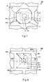
- FIG. 8is a plan view showing the structure of the main part of a vertical power MOSFET having a trench structure according to a first conventional example.
- FIG. 9Ais a sectional view along line IXA-IXA in FIG. 8
- FIG. 9Bis a sectional view along line IXB-IXB in FIG. 8 . As shown in FIGS.
- the vertical power MOSFET 400includes a semiconductor substrate 101 , a drift region 102 , a base region 103 , a source region 104 , a trench 105 , a gate oxide film 106 , a gate electrode 107 , a unit cell 108 , an interlayer insulating film 110 , a contact hole 111 , a source electrode 112 , and a drain electrode 113 .
- the drift region 102composed of an n ⁇ type semiconductor layer (low impurity concentration semiconductor layer) that is an epitaxial layer having a lower impurity concentration than the semiconductor substrate 101 is formed. Further, p-type impurity is ion-implanted into the n ⁇ semiconductor layer to form the p-type base region 103 . On the periphery of the p-type base region 103 is formed the trench 105 with a depth that reaches down to the drift region 102 .
- the trench structure of the first conventional exampleis a typical structure that is used most frequently.
- the gate oxide film 106is formed on the inner surface of the trench 105 .
- the gate electrode 107 made of polysilicon or the likeis formed on the gate oxide film 106 so as to fill the trench 105 .
- n-type impurityis ion-implanted into the surface of the p-type base region 103 to form the endless n+ type source region 104 along the trench 105 .
- the trench 105has a rectangular shape as shown in FIG. 8 .
- a trench gateis formed along a plane direction equivalent to a plane (100) on the Si (001) substrate surface, which is referred to herein as the plane [100].
- the interlayer insulating film 110has the contact hole 111 , through which the source electrode 112 is electrically connected to the p-type base region 103 and the n+ type source region 104 .
- the drain electrode 113is formed on the backside of the semiconductor substrate 101 which is opposite from the principal surface where the trench 105 is formed.
- a pn junction that is created in the interface between the drift region 102 and the base region 103is depleted of charge carriers due to reverse bias during Off-state.
- a FET inversion layeris formed on the side surface of the trench 105 , and thereby a current flows from the drain electrode 113 to the source electrode 112 as indicated by the arrow c in FIG. 9B . It is preferred to design the vertical power MOSFET so that On-state current is as high as possible with respect to Off-state withstand voltage.
- the vertical power MOSFETis used in connection with an inductor, reverse withstand voltage is applied between the drain and source during switch-off, and current flow beyond a certain design limit can result in breakdown of devices.
- a degree to tolerate breakdown currentis called device breakdown tolerance, and a device is preferably designed to have high breakdown tolerance.
- the device breakdown of the vertical power MOSFETis caused by the operation of NPN bipolar transistor, which is referred to herein as the parasitic bipolar transistor, where source, base and drain serve as emitter, base and collector, respectively. Specifically, if part of dielectric current flows into the base as shown by a current path d that is indicated by the arrow in FIG. 9B and a base voltage increases, the parasitic bipolar transistor turns on to apply positive feedback during a temperature increase and a current increase, which eventually causes device breakdown.
- FIG. 10is a plan view showing the structure of a main part of a vertical power MOSFET 500 having a trench structure according to the second conventional example.
- FIG. 11Ais a sectional view along line XIA-XIA in FIG. 10
- FIG. 11Bis a sectional view along line XIB-XIB in FIG. 10 .
- the same elements as in the vertical power MOSFET 400 of the first conventional exampleare denoted by the same reference symbols and not detailed herein.
- the vertical power MOSFET 500 of the second conventional examplehas a narrow source region 116 that is formed diagonally from a contact part of a unit cell where an electric field concentrates to the corners of the cell. Due to the presence of the narrow source region 116 , the length of a source part (L 5 in FIG. 11B ) along the diagonal of a cell is shorter than that (L 4 in FIG. 9B ) of the first conventional example. In this structure, the distance of a current path e (see FIG. 11B ) from the drain electrode to the source electrode is shorter than the distance of a current path d (see FIG. 9B ). This reduces the part where the current path e passes through the base, thereby lowering resistance in the base part. It is therefore possible to reduce an increase in base voltage that occurs when part of dielectric current flows into the base, which hinders the activation of the parasitic bipolar transistor. This allows suppressing a decrease in device breakdown tolerance.
- Japanese Unexamined Patent Publication No. 10-270689describes a technique that forms a side surface of a trench with the plane [100] and [110] so as to improve the uniformity of a gate insulating film and increase gate withstand voltage.
- Japanese Unexamined Patent Publication No. 09-213951describes a technique that makes the plane shape of a side surface of a trench octagon and quadrangle and forms their side surfaces with the plane [100] and [110].
- Japanese Unexamined Patent Publication No. 09-213951 and 2004-79955propose the structure that uses the plane [100] and [110] with high mobility for a trench side surface and preferably makes the plane [100] larger than the plane [110], thereby reducing on-resistance.
- the semiconductor apparatus according to Japanese Unexamined Patent Publication No. 2001-60688is unfavorable for the further reduction of cell size since it needs to place the narrow source region 116.
- the semiconductor apparatus according to Japanese Unexamined Patent Publication No. 09-213951is also unfavorable for the further reduction of cell size since the trench is composed of a combination of octagon and quadrangle shapes.
- the mere enlargement of the plane [100] with respect to the plane [110] that is proposed by Japanese Unexamined Patent Publication No. 09-213951 and 2004-79955can result in easy activation of a parasitic bipolar transistor due to an increase in base voltage.
- a semiconductor apparatusthat includes a semiconductor substrate of a first conductivity type, a base region of a second conductivity type formed on a principal surface of the semiconductor substrate, a trench has a substantially octagonal plane shape and formed in a periphery of the base region, and an endless source region of the first conductivity type formed on a surface of the base region along the trench.
- the principal planes on side surfaces of the trenchare composed of planes [100] and [110]. A minimum distance between the base region and the plane [110] facing each other through the source region is shorter than a minimum distance between the base region and the plane [100] facing each other through the source region.
- the present inventioncan prevent a decrease in device breakdown tolerance while achieving reduction of cell size. This is because of the following reasons.
- the present inventionforms the principal plane directions of the trench side surfaces with [100] and [110] and the trench has a substantially octagonal plane shape, it is possible to ease the concentration of current at a channel along a cell corner compared with a rectangular cell.
- the minimum distance between the base region and the trench side surface composed of the plane [110] that face each other through the source regionis shorter than the minimum distance between the base region and the trench side surface composed of the plane [100] that face each other through the source region, it is possible to reduce the distance that current passes through the base region as a whole in a unit cell compared with the case where the trench side surface is composed of only the plane [100] even when part of dielectric current flows into the base. This allows suppression of an increase in base voltage even if part of dielectric current flows into the base. As a result, this structure hinders the activation of a parasitic bipolar transistor, thus preventing a decrease in device breakdown tolerance.
- the trench of this embodimenthas a simple structure where the principal plane direction of the trench side surface is formed with [100] and [110], and the trench has a substantially octagonal plane shape, it is possible to achieve reduction in cell size.
- the present inventionhas a beneficial effect that provides a semiconductor apparatus capable of preventing a decrease in device breakdown tolerance and achieving reduction in cell size.
- FIG. 1is a plan view showing the configuration of the main part of a semiconductor apparatus according to an embodiment of the invention
- FIG. 2Ais a sectional view along line IIA-IIA of FIG. 1 ;
- FIG. 2Bis a sectional view along line IIB-IIB of FIG. 1 ;
- FIG. 3is an explanatory view showing a preferred range of W 2 according to an embodiment of the invention.
- FIG. 4Ais a process view showing a method of manufacturing a semiconductor apparatus according to an embodiment of the invention.
- FIG. 4Bis a process view showing a method of manufacturing a semiconductor apparatus according to an embodiment of the invention.
- FIG. 4Cis a process view showing a method of manufacturing a semiconductor apparatus according to an embodiment of the invention.
- FIG. 4Dis a process view showing a method of manufacturing a semiconductor apparatus according to an embodiment of the invention.
- FIG. 5Ais a process view showing a method of manufacturing a semiconductor apparatus according to an embodiment of the invention.
- FIG. 5Bis a process view showing a method of manufacturing a semiconductor apparatus according to an embodiment of the invention.
- FIG. 6is a plan view showing the configuration of the main part of a semiconductor apparatus according to an alternative embodiment 1;
- FIG. 7is a plan view showing the configuration of the main part of a semiconductor apparatus according to an alternative embodiment 2;
- FIG. 8is a plan view showing the configuration of the main part of a semiconductor apparatus according to a first conventional example
- FIG. 9Ais a sectional view along line IXA-IXA of FIG. 8 ;
- FIG. 9Bis a sectional view along line IXB-IXB of FIG. 8 ;
- FIG. 10is a plan view showing the configuration of the main part of a semiconductor apparatus according to a second conventional example
- FIG. 11Ais a sectional view along line XIA-XIA of FIG. 10 ;
- FIG. 11Bis a sectional view along line XIB-XIB of FIG. 10 .
- FIG. 1is a plan view showing the configuration of the main part of a vertical power MOSFET having a trench structure according to this embodiment.
- FIG. 2Ais a sectional view along line IIA-IIA of FIG. 1
- FIG. 2Bis a sectional view along line IIB-IIB of FIG. 1 . As shown in FIGS.
- the vertical power MOSFET 100includes a semiconductor substrate 1 , a drift region 2 , a base region 3 , a source region 4 , a trench 5 , a gate oxide film 6 , a gate electrode 7 , a unit cell 8 , an interlayer insulating film 10 , a contact hole 11 , a source electrode 12 , and a drain electrode 13 .
- the gate oxide film 6 , the gate electrode 7 , the interlayer insulating 10 and the source electrode 12are not illustrated for the sake of convenience in description.
- a position to create the contact hole 11is illustrated in dotted line.
- the semiconductor substrate 1is a silicon substrate and it is an n+ type semiconductor substrate (high impurity concentration semiconductor substrate), for example.
- the drift region 2composed of an n ⁇ type semiconductor layer (low impurity concentration semiconductor layer) that is an epitaxial layer having a lower impurity concentration than the semiconductor substrate 1 .
- p-type impurityis ion-implanted into the n ⁇ semiconductor layer to form the p-type base region 3 .
- the trench 5On the periphery of the p-type base region 3 is formed the trench 5 with a depth that reaches down to the drift region 2 .
- the gate oxide film 6is formed on the inner surface of the trench 5
- the gate electrode 7 made of polysilicon or the likeis formed on the gate oxide film 6 so as to fill the trench 5 .
- n-type impurityis ion-implanted into the surface of the p-type base region 3 to form the endless n+ type source region 4 along the trench 5 .
- the interlayer insulating film 10 and the source electrode 12are laminated in this order above the base region 3 , the source region 4 , the gate oxide film 6 and the gate electrode 7 as shown in FIGS. 2A and 2B .
- the interlayer insulating film 10has the contact hole 11 , through which the source electrode 12 is electrically connected to the p-type base region 3 and the n+ type source region 4 .
- the drain electrode 13is formed on the backside of the semiconductor substrate 1 which is opposite from the surface where the trench 5 is formed.
- the vertical power MOSFET 100 having the trench structure of this embodimentincludes a plurality of (for example, several hundreds of thousands of) unit cells with trench structure.
- a pn junction that is created in the interface between the drift region 2 and the base region 3is depleted of charge carriers due to reverse bias during Off-state.
- a FET inversion layeris formed on the side surface of the trench 5 , and thereby current flows from the drain electrode 13 to the source electrode 12 as indicated by a current path a in FIG. 1 .
- the interior angle of the intersection of adjacent side surfacesis 135°.
- the plane shape of the trench 5 formed on the Si (001) substrateis an octagon.
- the plane directions equivalent to the planes (100) and (110) on the Si (001) substrateare referred to herein as [100] and [110], respectively.
- the principal plane direction of the side surface of the trench 5is composed of [100] and [110].
- a minimum distance L 2 between the base region 3 and the plane [110] of the side surface of the trench 5is designed to be shorter than a minimum distance L 1 between the base region 3 and the plane [100] of the side surface of the trench 5 as represented by the following expression: L 1 >L 2 Expression 1
- this embodimentallows reduction in cell size since the structure is as simple as forming the principal planes of the trench with [100] and [110] and setting the interior angle of the trench to 135°.
- the semiconductor apparatus of this embodimentis configured so as to satisfy the following expression where the length of the side (first side) of the plane [100] of the side surface (first side surface) of the trench 5 in the horizontal direction of the semiconductor substrate 1 is W 1 and the length of the side (second side) of the plane [110] of the side surface (second side surface) of the trench 5 is W 2 : W1>W2 Expression 2 W 1 and W 2 are symbols that represent both each side itself and the length of each side.
- the plane shape of the base region 3 of this embodimentis substantially square as shown in FIG. 1 .
- the side surfaces of the base region 3are composed of four surfaces that are parallel with the side surface planes [100] of the trench 5 .
- a side of a substantial square that forms the plane shape of the base region 3is indicated by Da.
- a minimum distance between the plane [100] of the side surface of the trench 5 and the plane [100] of the opposite side surface of the trench 5is indicated by d.
- Dais a symbol that represents both a side itself and the length of the side.
- L 1 and L 2are given by Expressions 3 and 4 below. W 1 and W 2 satisfy the relationship represented by Expression 5.
- an intersection of perpendicular bisectors of Da adjacent to each other in the base regionsubstantially corresponds to an intersection of perpendicular bisectors of two sides W 1 adjacent to each other through W 2 .
- substitution of Expressions 3 and 4 into Expression 1gives the following expressions: W 2>( ⁇ square root over (2) ⁇ 1) ⁇ ( d ⁇ D a ) ⁇ 0.41 ⁇ ( d ⁇ D a ) Expression 6 W 1 ⁇ ( ⁇ square root over (2) ⁇ 1) ⁇ d +(2 ⁇ square root over (2) ⁇ ) ⁇ D a ⁇ 0.41 d +0.59 D a Expression 7
- FIG. 3is a graph showing the relationship of Expressions 2, 5 and 6.
- the horizontal axisindicates W 2 and the vertical axis indicates W 1
- the region of the dual directional arrow Pis a preferred range of W 2 . Since W 1 is preferably as large as possible as described earlier, it is preferred in the region of the dual directional arrow P that W 2 is as small as possible, that is, W 1 is as large as possible.
- the setting conditions of the length of W 1 in the plane [100]may be the following Expression 8 instead of Expression 7 mentioned above.
- W 1 ′W 1+ ⁇ square root over (2) ⁇ ( r ⁇ 1) ⁇ ( d ⁇ D a ) Expression 8
- the gate oxide film 6is formed by thermally oxidizing the surface of the trench 5 at a temperature of about 850° C., for example.
- the oxide filmis thicker in the plane [110] than in the plane [100] due to plane direction dependency in oxidation speed.
- the oxide film of the plane [110]is thicker than the oxide film of the plane [100]
- the transconductance value in the plane [110]is smaller than the transconductance value in the plane [100].
- a ratio r of transconductance between the plane [100] and the plane [110]is represented by the following expression:
- a base voltage dropis proportional to base current and the length of the source region. Therefore, the conditions where a base voltage drop between a channel and a contact during breakdown does not reach its maximum at least when passing through the current path b is represented by the following expression: g m1 ⁇ L 1 >g m2 ⁇ L 2 Expression 10
- Expression 8can be derived from Expressions 9, 10, 3 and 4.
- the length of one side of the plane [100]may be larger than the value of W 1 of Expression 7 in accordance with the ratio r (>1) of transconductance. This increases the mobility of electrons in a channel region more effectively, thereby improving the performance of power MOSFET.
- FIGS. 4A to 4D , 5 A and 5 Bare all sectional views along line IIA-IIA in FIG. 1 .
- the following manufacturing processis a typical example, and other manufacturing processes may be used as long they do not deviate from the gist of the present invention.
- the n ⁇ type semiconductor layer 9that has a lower impurity concentration than the semiconductor substrate 1 is epitaxially grown. Then, the trench 5 of 1 to 2 ⁇ m is formed in the n ⁇ type semiconductor layer 9 ( 2 ) at the position to be the periphery of the p type base region 3 , which is described later, by photolithography process. It is then segmented into a plurality of unit cells 8 .
- the photolithography processuses a photoresist film which is patterned into a shape that cuts four corners of a square at 45°. This embodiment forms the trench whose principal planes are composed of [100] and [110] and whose plane shape is an octagon.
- the gate oxide film 6is formed on the whole area including the trench 5 by thermal oxidation.
- a polysilicon filmis then formed on the whole area by Chemical Vapor Deposition (CVD). After that, phosphorous diffusion and etch-back are performed successively so as to remove an unnecessary part of the polysilicon film so that it is left only inside the trench 5 , thereby forming the gate electrode 7 .
- the p type base region 3 with the depth of 1 to 2 ⁇ mis formed all over the n ⁇ type semiconductor layer 9 ( 2 ) that is surrounded by the trenches 5 .
- annealingis performed for 10 to 20 minutes at a temperature of 1100° C. to 1200° C.
- the n+ source region 4is formed. Specifically, ion implantation using arsenic (As) as n ⁇ type impurity is performed on the surface of the p type base region 3 in endless form along the trench by using a photoresist film which is patterned into the shape that corresponds to the base region as shown in FIGS. 2A and 2B as a mask. After that, annealing is performed for 25 to 35 minutes at a temperature of 980° C. to 1050° C., for example. The thickness of the n+ source region 4 is 0.4 to 0.8 ⁇ m, for example.
- the interlayer insulating film 10is formed by CVD, and the gate oxide film 6 and the interlayer insulating film 10 are patterned to form the contact opening 11 .
- the source electrode 12is formed to fill the contact opening 11 .
- the manufacturing method of the semiconductor apparatususes a process that is as simple as forming the side surfaces of the trench with [100] and [110] and setting the interior angle of the intersection of adjacent trench side surfaces to 135°, it is possible to achieve reduction in cell size without substantially changing processing accuracy compared with a conventional structure.
- this manufacturing methodperforms formation of the base region 3 and the source region 4 that requires high temperature processing after forming the trench 5 , it is possible to form a trench structure with stable properties without thermally affecting the trench 5 and a semiconductor crystal in the vicinity of the trench 5 .
- the-minimum distance L 2 between the base region 3 and the trench side surface composed of the plane [110] that face each other through the source region 4is shorter than the minimum distance L 1 between the base region 3 and the trench side surface composed of the plane [100] that face each other through the source region 4 , it is possible to reduce the distance that current passes through the base region 3 as a whole in a unit cell when part of dielectric current flows into the base region 3 . This lowers entire base resistance even if part of dielectric current flows into the base region 3 , thereby suppressing an increase in base voltage. It is therefore possible to hinder the activation of a parasitic bipolar transistor, thus preventing a decrease in device breakdown tolerance.
- the plane shape of the source region 4is substantially square in the above embodiment, it is not limited thereto, and other shapes may be used as long as the minimum distance L 2 between the base region 3 and the trench side surface composed of the plane [110] that face each other through the source region 4 is shorter than the minimum distance L 1 between the base region 3 and the trench side surface composed of the plane [100] that face each other through the source region 4 .
- the above embodimentdescribes a case where the lengths of the sides of the plane [100] of the semiconductor substrate 1 in the horizontal direction and the lengths of the sides of the plane [110] of the semiconductor substrate 1 in the horizontal direction are all the same, it is feasible to use a combination of the plane [100] and the plane [110] with different side lengths in a unit cell. It is also feasible that the plane shape of the trench is different in a different unit cell.
- FIG. 6is a plan view showing the trench structure of the alternative embodiment 1.
- the same elements as in the above embodimentare denoted by the same reference symbols and not detailed herein.
- the semiconductor apparatus 200 of the alternative embodiment 1has basically the same structure as the above embodiment except for the following points.
- the trench 5 of the above embodimentis an octagon having W 1 and W 2
- a trench 5 a of this alternative embodimentis an octagon having W 1 , W 2 and W 3 as shown in FIG. 6 .
- the base region 3 of the above embodimenthas a substantially square plane shape
- a base region 3 a of this alternative embodimenthas a substantially rectangle plane shape.
- the sides of the plane [100] on the side surface of the trench 5 aare indicated by W 1 and W 3 where W 1 ⁇ W 3
- the length of the side (third side) of the plane [110] on the side surface of the trench 5 ais indicated by W 2 .
- the side (fourth side) of the base region 3 a that is parallel with W 1is indicated by Da and the side (fifth side) of the base region 3 a that is parallel with W 3 is indicated by Db.
- values of W 1 and W 2are determined firstly so as to optimize the shape of a substantially square base region whose one side has a length of Da that serves as a short side of the base region 3 . Then, a value of W 3 is determined so that an intersection of perpendicular bisectors of Da and Db that are adjacent to each other in the base region 3 a substantially corresponds to an intersection of perpendicular bisectors of W 1 and W 3 that are adjacent to each other through W 2 , and a minimum distance from a mid point of W 1 to the base region 3 a and a minimum distance from a mid point of W 3 to the base region 3 a are substantially the same.
- Expressions 11 to 14It is desirable to satisfy Expressions 11 to 14. It is more desirable to replace Expression 11 with Expression 15 so as to satisfy Expressions 12 to 15. Satisfying Expressions 11 to 14 or 12 to 15 allows setting large values to W 1 and W 3 while setting the minimum distance L 2 between the base region 3 a and the plane [110] of the side surface of the trench 5 a to be shorter than the minimum distance L 1 between the base region 3 a and the plane [100] of the side surface of the trench 5 a in the case where the plane shape of the base region 3 a is rectangular. It is therefore possible to increase the mobility of electrons in a channel region to improve the performance of the power MOSFET while preventing a decrease in device breakdown tolerance due to the same reasons as the above embodiment. It is also possible to achieve reduction in cell size as is the case with the above embodiment.
- FIG. 7is a plan view showing the trench structure of the alternative embodiment 2.
- the semiconductor apparatus 300 of the alternative embodiment 2has basically the same structure as the above embodiment except for the following points.
- the internal angle of adjacent side surfaces of the base region 3is 90° in the above embodiment, a corner between adjacent side surfaces of the base region 3 b is rounded in this embodiment as shown in FIG. 7 .
- the source region 4includes an electrode connecting area that connects a source electrode.
- the electrode connecting areahas four sides that are parallel with the plane [100] and corners that are rounded.
- This structureallows easing the concentration of base current density at a base corner part. It is therefore possible to suppress a base voltage drop more effectively.
Landscapes
- Electrodes Of Semiconductors (AREA)
Abstract
Description
1. Field of the Invention
The present invention is related to a semiconductor apparatus having a trench structure and a method of manufacturing the same.
2. Description of Related Art
A power metal-oxide semiconductor field-effect transistor (MOSFET) is a typical semiconductor apparatus that has both a high withstand voltage and a large current capacity. There are two types of power MOSFET: lateral power MOSFET and vertical power MOSFET. The lateral power MOSFET is designed so that operating current (drain current) flows horizontally through a semiconductor substrate. The vertical power MOSFET is designed so that drain current flows vertically through a semiconductor substrate. The vertical power MOSFET has become common since it is superior to the lateral power MOSFET in being easy to realize a high density unit cell structure and thus allowing an increase in on-current. Particularly distinguished is a vertical power MOSFET having a trench structure where a channel is perpendicular to a substrate, which is described in Japanese Unexamined Patent Publication No. 2001-60688, 10-270689, 09-213951, 2004-79955 and 2004-55976, for example.
In thevertical power MOSFET 400 of the first conventional example, on an n+ type semiconductor substrate (high impurity concentration semiconductor substrate)101, thedrift region 102 composed of an n− type semiconductor layer (low impurity concentration semiconductor layer) that is an epitaxial layer having a lower impurity concentration than thesemiconductor substrate 101 is formed. Further, p-type impurity is ion-implanted into the n− semiconductor layer to form the p-type base region 103. On the periphery of the p-type base region 103 is formed thetrench 105 with a depth that reaches down to thedrift region 102. The trench structure of the first conventional example is a typical structure that is used most frequently.
Thegate oxide film 106 is formed on the inner surface of thetrench 105. Thegate electrode 107 made of polysilicon or the like is formed on thegate oxide film 106 so as to fill thetrench 105. Further, n-type impurity is ion-implanted into the surface of the p-type base region 103 to form the endless n+type source region 104 along thetrench 105. Thetrench 105 has a rectangular shape as shown inFIG. 8 . A trench gate is formed along a plane direction equivalent to a plane (100) on the Si (001) substrate surface, which is referred to herein as the plane [100].
Above the p-type base region 103, the n+type source region 104, thegate oxide film 106 and thegate electrode 107 are theinterlayer insulating film 110 and thesource electrode 112 which are laminated in this order. Theinterlayer insulating film 110 has thecontact hole 111, through which thesource electrode 112 is electrically connected to the p-type base region 103 and the n+type source region 104. Thedrain electrode 113 is formed on the backside of thesemiconductor substrate 101 which is opposite from the principal surface where thetrench 105 is formed.
In the vertical power MOSFET having such a structure, a pn junction that is created in the interface between thedrift region 102 and thebase region 103 is depleted of charge carriers due to reverse bias during Off-state. During On-state, on the other hand, a FET inversion layer is formed on the side surface of thetrench 105, and thereby a current flows from thedrain electrode 113 to thesource electrode 112 as indicated by the arrow c inFIG. 9B . It is preferred to design the vertical power MOSFET so that On-state current is as high as possible with respect to Off-state withstand voltage.
Since the vertical power MOSFET is used in connection with an inductor, reverse withstand voltage is applied between the drain and source during switch-off, and current flow beyond a certain design limit can result in breakdown of devices. A degree to tolerate breakdown current is called device breakdown tolerance, and a device is preferably designed to have high breakdown tolerance.
It is important for the vertical power MOSFET to prevent device breakdown. The device breakdown of the vertical power MOSFET is caused by the operation of NPN bipolar transistor, which is referred to herein as the parasitic bipolar transistor, where source, base and drain serve as emitter, base and collector, respectively. Specifically, if part of dielectric current flows into the base as shown by a current path d that is indicated by the arrow inFIG. 9B and a base voltage increases, the parasitic bipolar transistor turns on to apply positive feedback during a temperature increase and a current increase, which eventually causes device breakdown.
In the first conventional example described above, current is likely to concentrate at a cell corner of a rectangular trench. Breakdown thereby tends to occur at the cell corner and its vicinity, which can cause the parasitic bipolar transistor to turn on.
Japanese Unexamined Patent Publication No. 2001-60688 mentioned above, which is referred to herein as a second conventional example, proposes a structure to prevent a decrease in device breakdown tolerance.FIG. 10 is a plan view showing the structure of a main part of avertical power MOSFET 500 having a trench structure according to the second conventional example.FIG. 11A is a sectional view along line XIA-XIA inFIG. 10 , andFIG. 11B is a sectional view along line XIB-XIB inFIG. 10 . In the following description, the same elements as in thevertical power MOSFET 400 of the first conventional example are denoted by the same reference symbols and not detailed herein.
Thevertical power MOSFET 500 of the second conventional example has anarrow source region 116 that is formed diagonally from a contact part of a unit cell where an electric field concentrates to the corners of the cell. Due to the presence of thenarrow source region 116, the length of a source part (L5inFIG. 11B ) along the diagonal of a cell is shorter than that (L4inFIG. 9B ) of the first conventional example. In this structure, the distance of a current path e (seeFIG. 11B ) from the drain electrode to the source electrode is shorter than the distance of a current path d (seeFIG. 9B ). This reduces the part where the current path e passes through the base, thereby lowering resistance in the base part. It is therefore possible to reduce an increase in base voltage that occurs when part of dielectric current flows into the base, which hinders the activation of the parasitic bipolar transistor. This allows suppressing a decrease in device breakdown tolerance.
Japanese Unexamined Patent Publication No. 10-270689 describes a technique that forms a side surface of a trench with the plane [100] and [110] so as to improve the uniformity of a gate insulating film and increase gate withstand voltage. Japanese Unexamined Patent Publication No. 09-213951 describes a technique that makes the plane shape of a side surface of a trench octagon and quadrangle and forms their side surfaces with the plane [100] and [110]. Further, Japanese Unexamined Patent Publication No. 09-213951 and 2004-79955 propose the structure that uses the plane [100] and [110] with high mobility for a trench side surface and preferably makes the plane [100] larger than the plane [110], thereby reducing on-resistance.
As electronic equipment achieve small-size, light-weight, high-speed operation and high-frequency performance, the need increases for higher density integration of a semiconductor device to be mounted on the electronic equipment. It is thus strongly required for vertical power MOSFET to further reduce the cell size while preventing a decrease in device breakdown tolerance.
However, the semiconductor apparatus according to Japanese Unexamined Patent Publication No. 2001-60688 is unfavorable for the further reduction of cell size since it needs to place thenarrow source region 116. The semiconductor apparatus according to Japanese Unexamined Patent Publication No. 09-213951 is also unfavorable for the further reduction of cell size since the trench is composed of a combination of octagon and quadrangle shapes. Further, the mere enlargement of the plane [100] with respect to the plane [110] that is proposed by Japanese Unexamined Patent Publication No. 09-213951 and 2004-79955 can result in easy activation of a parasitic bipolar transistor due to an increase in base voltage.
According to an embodiment of the invention, there is provided a semiconductor apparatus that includes a semiconductor substrate of a first conductivity type, a base region of a second conductivity type formed on a principal surface of the semiconductor substrate, a trench has a substantially octagonal plane shape and formed in a periphery of the base region, and an endless source region of the first conductivity type formed on a surface of the base region along the trench. In this semiconductor apparatus, the principal planes on side surfaces of the trench are composed of planes [100] and [110]. A minimum distance between the base region and the plane [110] facing each other through the source region is shorter than a minimum distance between the base region and the plane [100] facing each other through the source region.
With this configuration, the present invention can prevent a decrease in device breakdown tolerance while achieving reduction of cell size. This is because of the following reasons.
Since the present invention forms the principal plane directions of the trench side surfaces with [100] and [110] and the trench has a substantially octagonal plane shape, it is possible to ease the concentration of current at a channel along a cell corner compared with a rectangular cell.
Further, since the minimum distance between the base region and the trench side surface composed of the plane [110] that face each other through the source region is shorter than the minimum distance between the base region and the trench side surface composed of the plane [100] that face each other through the source region, it is possible to reduce the distance that current passes through the base region as a whole in a unit cell compared with the case where the trench side surface is composed of only the plane [100] even when part of dielectric current flows into the base. This allows suppression of an increase in base voltage even if part of dielectric current flows into the base. As a result, this structure hinders the activation of a parasitic bipolar transistor, thus preventing a decrease in device breakdown tolerance.
Furthermore, since the trench of this embodiment has a simple structure where the principal plane direction of the trench side surface is formed with [100] and [110], and the trench has a substantially octagonal plane shape, it is possible to achieve reduction in cell size.
As described above, the present invention has a beneficial effect that provides a semiconductor apparatus capable of preventing a decrease in device breakdown tolerance and achieving reduction in cell size.
The above and other objects, advantages and features of the present invention will be more apparent from the following description taken in conjunction with the accompanying drawings, in which:
The invention will be now described herein with reference to illustrative embodiments. Those skilled in the art will recognize that many alternative embodiments can be accomplished using the teachings of the present invention and that the invention is not limited to the embodiments illustrated for explanatory purposed.
Thesemiconductor substrate 1 is a silicon substrate and it is an n+ type semiconductor substrate (high impurity concentration semiconductor substrate), for example. On thesemiconductor substrate 1 is formed thedrift region 2 composed of an n− type semiconductor layer (low impurity concentration semiconductor layer) that is an epitaxial layer having a lower impurity concentration than thesemiconductor substrate 1. Further, p-type impurity is ion-implanted into the n− semiconductor layer to form the p-type base region 3.
On the periphery of the p-type base region 3 is formed thetrench 5 with a depth that reaches down to thedrift region 2. Thegate oxide film 6 is formed on the inner surface of thetrench 5, and thegate electrode 7 made of polysilicon or the like is formed on thegate oxide film 6 so as to fill thetrench 5. Further, n-type impurity is ion-implanted into the surface of the p-type base region 3 to form the endless n+type source region 4 along thetrench 5.
Theinterlayer insulating film 10 and thesource electrode 12 are laminated in this order above thebase region 3, thesource region 4, thegate oxide film 6 and thegate electrode 7 as shown inFIGS. 2A and 2B . Theinterlayer insulating film 10 has thecontact hole 11, through which thesource electrode 12 is electrically connected to the p-type base region 3 and the n+type source region 4. Thedrain electrode 13 is formed on the backside of thesemiconductor substrate 1 which is opposite from the surface where thetrench 5 is formed.
Thevertical power MOSFET 100 having the trench structure of this embodiment includes a plurality of (for example, several hundreds of thousands of) unit cells with trench structure. In thevertical power MOSFET 100, a pn junction that is created in the interface between thedrift region 2 and thebase region 3 is depleted of charge carriers due to reverse bias during Off-state. During On-state, on the other hand, a FET inversion layer is formed on the side surface of thetrench 5, and thereby current flows from thedrain electrode 13 to thesource electrode 12 as indicated by a current path a inFIG. 1 .
The configuration of a unit cell of thevertical power MOSFET 100 according to this embodiment is described in detail below.
As shown inFIG. 1 , in thetrench 5 of thevertical power MOSFET 100 of this embodiment, the interior angle of the intersection of adjacent side surfaces is 135°. The plane shape of thetrench 5 formed on the Si (001) substrate is an octagon. The plane directions equivalent to the planes (100) and (110) on the Si (001) substrate are referred to herein as [100] and [110], respectively.
The principal plane direction of the side surface of thetrench 5 is composed of [100] and [110]. A minimum distance L2between thebase region 3 and the plane [110] of the side surface of thetrench 5 is designed to be shorter than a minimum distance L1between thebase region 3 and the plane [100] of the side surface of thetrench 5 as represented by the following expression:
L1>L2 Expression 1
L1>L2 Expression 1
Setting the interior angle of the intersection of adjacent side surfaces of thetrench 5 to substantially 135° allows easing the concentration of current at a channel along the cell corner compared with a rectangular cell. Further, since the minimum distance L2between thebase region 3 and the trench side surface composed of the plane [110] that face each other through thesource region 4 is shorter than the minimum distance L1between thebase region 3 and the trench side surface composed of the plane [100] that face each other through thesource region 4, it allows the distance that current passes through thebase region 3 as a whole in a unit cell when part of dielectric current flows into thebase region 3 to be shorter than that in the case where the trench side surface is composed of only the plane [100]. This lowers entire base resistance, thereby suppressing an increase in base voltage even when part of dielectric current flows into thebase region 3.
The activation of a parasitic bipolar transistor is thereby hindered, thus preventing a decrease in device breakdown tolerance. It is therefore possible to provide a reliable semiconductor apparatus.
Further, this embodiment allows reduction in cell size since the structure is as simple as forming the principal planes of the trench with [100] and [110] and setting the interior angle of the trench to 135°.
The semiconductor apparatus of this embodiment is configured so as to satisfy the following expression where the length of the side (first side) of the plane [100] of the side surface (first side surface) of thetrench 5 in the horizontal direction of thesemiconductor substrate 1 is W1 and the length of the side (second side) of the plane [110] of the side surface (second side surface) of thetrench 5 is W2:
W1>W2Expression 2
W1 and W2 are symbols that represent both each side itself and the length of each side.
W1>W2
W1 and W2 are symbols that represent both each side itself and the length of each side.
By satisfyingExpression 2, it is possible to increase the mobility of electrons in a channel region to improve the performance of power MOSFET. Further, in the conditions ofExpression 2, current density is higher in the vicinity of the plane [110] having W2 than in the vicinity of the plane [100] having W1. However, since base resistance is lowered in the vicinity of the plane [110] by reducing the length of the source region (L2) to shorten a distance that dielectric current passes through the base, an increase in base voltage is suppressed even when part of dielectric current flows through the current path b. It is thereby possible to reduce an increase in base voltage so as to hinder the activation of a parasitic bipolar transistor, thus preventing a decrease in device breakdown tolerance.
The plane shape of thebase region 3 of this embodiment is substantially square as shown inFIG. 1 . The side surfaces of thebase region 3 are composed of four surfaces that are parallel with the side surface planes [100] of thetrench 5. A side of a substantial square that forms the plane shape of thebase region 3 is indicated by Da. A minimum distance between the plane [100] of the side surface of thetrench 5 and the plane [100] of the opposite side surface of thetrench 5 is indicated by d. Da is a symbol that represents both a side itself and the length of the side. L1and L2are given byExpressions Expression 5.
In this embodiment, an intersection of perpendicular bisectors of Da adjacent to each other in the base region substantially corresponds to an intersection of perpendicular bisectors of two sides W1 adjacent to each other through W2. In this case, substitution ofExpressions Expression 1 gives the following expressions:
W2>(√{square root over (2)}−1)·(d−Da)≈0.41·(d−Da)Expression 6
W1<(√{square root over (2)}−1)·d+(2−√{square root over (2)})·Da≈0.41d+0.59Da Expression 7
W2>(√{square root over (2)}−1)·(d−Da)≈0.41·(d−Da)
W1<(√{square root over (2)}−1)·d+(2−√{square root over (2)})·Da≈0.41d+0.59Da Expression 7
By setting the value of W1 as large as possible in the range that satisfiesExpression 1, it is possible to prevent a decrease in device breakdown tolerance and improve the reliability while improving the performance of power MOSFET. Setting a large value to W1 allows increasing the mobility of electrons in a channel region, thereby improving the performance of power MOSFET. Further, in the conditions ofExpression 2, current density is higher in the vicinity of the plane [110] with W2 than in the vicinity of the plane [100] with W1. However,satisfying Expressions FIG. 2B , thereby suppressing an increase in base voltage. It is therefore possible to reduce an increase in base voltage so as to hinder the activation of a parasitic bipolar transistor, thus preventing a decrease in device breakdown tolerance.
In this embodiment, the setting conditions of the length of W1 in the plane [100] may be the followingExpression 8 instead ofExpression 7 mentioned above.
W1′=W1+√{square root over (2)}·(r−1)·(d−Da)Expression 8
W1′=W1+√{square root over (2)}·(r−1)·(d−Da)
This is because of the following reasons. Thegate oxide film 6 is formed by thermally oxidizing the surface of thetrench 5 at a temperature of about 850° C., for example. In this case, the oxide film is thicker in the plane [110] than in the plane [100] due to plane direction dependency in oxidation speed. As a result that the oxide film of the plane [110] is thicker than the oxide film of the plane [100], the transconductance value in the plane [110] is smaller than the transconductance value in the plane [100].
If the oxide film thickness of the plane [100] is t1, the oxide film thickness of the plane [110] is t2, the transconductance value in the plane [100] is gm1, and the transconductance value in the plane [110] is gm2, a ratio r of transconductance between the plane [100] and the plane [110] is represented by the following expression:
A base voltage drop is proportional to base current and the length of the source region. Therefore, the conditions where a base voltage drop between a channel and a contact during breakdown does not reach its maximum at least when passing through the current path b is represented by the following expression:
gm1·L1>gm2·L2 Expression 10
gm1·L1>gm2·L2 Expression 10
As obvious fromExpression 8, the length of one side of the plane [100] may be larger than the value of W1 ofExpression 7 in accordance with the ratio r (>1) of transconductance. This increases the mobility of electrons in a channel region more effectively, thereby improving the performance of power MOSFET.
A method of manufacturing a semiconductor apparatus according to this embodiment is described hereinafter with reference toFIGS. 4A to 4D ,5A and5B.FIGS. 4A to 4D ,5A and5B are all sectional views along line IIA-IIA inFIG. 1 . The following manufacturing process is a typical example, and other manufacturing processes may be used as long they do not deviate from the gist of the present invention.
Referring first toFIG. 4A , on thesemiconductor substrate 1 such as an n+ type semiconductor substrate made of silicon whose surface is a plane (100), the n−type semiconductor layer 9 that has a lower impurity concentration than thesemiconductor substrate 1 is epitaxially grown. Then, thetrench 5 of 1 to 2 μm is formed in the n− type semiconductor layer9 (2) at the position to be the periphery of the ptype base region 3, which is described later, by photolithography process. It is then segmented into a plurality ofunit cells 8. The photolithography process uses a photoresist film which is patterned into a shape that cuts four corners of a square at 45°. This embodiment forms the trench whose principal planes are composed of [100] and [110] and whose plane shape is an octagon.
Referring next toFIG. 4B , thegate oxide film 6 is formed on the whole area including thetrench 5 by thermal oxidation. A polysilicon film is then formed on the whole area by Chemical Vapor Deposition (CVD). After that, phosphorous diffusion and etch-back are performed successively so as to remove an unnecessary part of the polysilicon film so that it is left only inside thetrench 5, thereby forming thegate electrode 7.
Referring then toFIG. 4C , the ptype base region 3 with the depth of 1 to 2 μm is formed all over the n− type semiconductor layer9 (2) that is surrounded by thetrenches 5. For example, after ion implantation using boron B as p-type impurity, annealing is performed for 10 to 20 minutes at a temperature of 1100° C. to 1200° C.
Referring then toFIG. 4D , then+ source region 4 is formed. Specifically, ion implantation using arsenic (As) as n− type impurity is performed on the surface of the ptype base region 3 in endless form along the trench by using a photoresist film which is patterned into the shape that corresponds to the base region as shown inFIGS. 2A and 2B as a mask. After that, annealing is performed for 25 to 35 minutes at a temperature of 980° C. to 1050° C., for example. The thickness of then+ source region 4 is 0.4 to 0.8 μm, for example.
Referring then toFIG. 5A , theinterlayer insulating film 10 is formed by CVD, and thegate oxide film 6 and theinterlayer insulating film 10 are patterned to form thecontact opening 11. Referring finally toFIG. 5B , thesource electrode 12 is formed to fill thecontact opening 11.
Since the manufacturing method of the semiconductor apparatus according to this embodiment uses a process that is as simple as forming the side surfaces of the trench with [100] and [110] and setting the interior angle of the intersection of adjacent trench side surfaces to 135°, it is possible to achieve reduction in cell size without substantially changing processing accuracy compared with a conventional structure.
Further, since this manufacturing method performs formation of thebase region 3 and thesource region 4 that requires high temperature processing after forming thetrench 5, it is possible to form a trench structure with stable properties without thermally affecting thetrench 5 and a semiconductor crystal in the vicinity of thetrench 5.
Furthermore, since the-minimum distance L2between thebase region 3 and the trench side surface composed of the plane [110] that face each other through thesource region 4 is shorter than the minimum distance L1between thebase region 3 and the trench side surface composed of the plane [100] that face each other through thesource region 4, it is possible to reduce the distance that current passes through thebase region 3 as a whole in a unit cell when part of dielectric current flows into thebase region 3. This lowers entire base resistance even if part of dielectric current flows into thebase region 3, thereby suppressing an increase in base voltage. It is therefore possible to hinder the activation of a parasitic bipolar transistor, thus preventing a decrease in device breakdown tolerance.
Though the plane shape of thesource region 4 is substantially square in the above embodiment, it is not limited thereto, and other shapes may be used as long as the minimum distance L2between thebase region 3 and the trench side surface composed of the plane [110] that face each other through thesource region 4 is shorter than the minimum distance L1between thebase region 3 and the trench side surface composed of the plane [100] that face each other through thesource region 4. Further, though the above embodiment describes a case where the lengths of the sides of the plane [100] of thesemiconductor substrate 1 in the horizontal direction and the lengths of the sides of the plane [110] of thesemiconductor substrate 1 in the horizontal direction are all the same, it is feasible to use a combination of the plane [100] and the plane [110] with different side lengths in a unit cell. It is also feasible that the plane shape of the trench is different in a different unit cell.
An alternative embodiment having a trench structure that is different from the above embodiment is described hereinafter.FIG. 6 is a plan view showing the trench structure of thealternative embodiment 1. In the following description, the same elements as in the above embodiment are denoted by the same reference symbols and not detailed herein.
Thesemiconductor apparatus 200 of thealternative embodiment 1 has basically the same structure as the above embodiment except for the following points. Though thetrench 5 of the above embodiment is an octagon having W1 and W2, atrench 5aof this alternative embodiment is an octagon having W1, W2 and W3 as shown inFIG. 6 . Further, though thebase region 3 of the above embodiment has a substantially square plane shape, abase region 3aof this alternative embodiment has a substantially rectangle plane shape.
Specifically, the sides of the plane [100] on the side surface of thetrench 5aare indicated by W1 and W3 where W1<W3, and the length of the side (third side) of the plane [110] on the side surface of thetrench 5ais indicated by W2. The side (fourth side) of thebase region 3athat is parallel with W1 is indicated by Da and the side (fifth side) of thebase region 3athat is parallel with W3 is indicated by Db.
In the case where the plane shape of the base region is substantially rectangular, values of W1 and W2 are determined firstly so as to optimize the shape of a substantially square base region whose one side has a length of Da that serves as a short side of thebase region 3. Then, a value of W3 is determined so that an intersection of perpendicular bisectors of Da and Db that are adjacent to each other in thebase region 3asubstantially corresponds to an intersection of perpendicular bisectors of W1 and W3 that are adjacent to each other through W2, and a minimum distance from a mid point of W1 to thebase region 3aand a minimum distance from a mid point of W3 to thebase region 3aare substantially the same. In sum, the positions of thetrench 5aand thebase region 3aare determined so as to satisfy the following expressions:
Db≧Da, W3≧W1 Expression 11
W1>W2Expression 12
W1=d−√{square root over (2)}·W 2 Expression 13
W2>(√{square root over (2)}−1)·(d−Da) Expression 14
Db−Da=W3−W1≧0 Expression 15
Db≧Da, W3≧
W1>W2
W1=d−√{square root over (2)}·
W2>(√{square root over (2)}−1)·(d−Da) Expression 14
Db−Da=W3−W1≧0 Expression 15
It is desirable to satisfyExpressions 11 to 14. It is more desirable to replaceExpression 11 with Expression 15 so as to satisfyExpressions 12 to 15.Satisfying Expressions 11 to 14 or 12 to 15 allows setting large values to W1 and W3 while setting the minimum distance L2between thebase region 3aand the plane [110] of the side surface of thetrench 5ato be shorter than the minimum distance L1between thebase region 3aand the plane [100] of the side surface of thetrench 5ain the case where the plane shape of thebase region 3ais rectangular. It is therefore possible to increase the mobility of electrons in a channel region to improve the performance of the power MOSFET while preventing a decrease in device breakdown tolerance due to the same reasons as the above embodiment. It is also possible to achieve reduction in cell size as is the case with the above embodiment.
An alternative embodiment having a trench structure that is different from the above embodiment is described hereinafter.FIG. 7 is a plan view showing the trench structure of thealternative embodiment 2.
Thesemiconductor apparatus 300 of thealternative embodiment 2 has basically the same structure as the above embodiment except for the following points. Though the internal angle of adjacent side surfaces of thebase region 3 is 90° in the above embodiment, a corner between adjacent side surfaces of thebase region 3bis rounded in this embodiment as shown inFIG. 7 . In other words, thesource region 4 includes an electrode connecting area that connects a source electrode. The electrode connecting area has four sides that are parallel with the plane [100] and corners that are rounded.
This structure allows easing the concentration of base current density at a base corner part. It is therefore possible to suppress a base voltage drop more effectively.
It is apparent that the present invention is not limited to the above embodiment that may be modified and changed without departing from the scope and spirit of the invention.
Claims (19)
1. A semiconductor apparatus comprising:
a semiconductor substrate of a first conductivity type;
a base region of a second conductivity type formed on a principal surface of the semiconductor substrate;
a trench having a substantially octagonal plane shape and formed in a periphery of the base region; and
a source region of the first conductivity type formed on a surface of the base region along the trench, wherein
principal planes on side surfaces of the trench are composed of: a first plane [100] that faces the base region through the source region and a second plane [110] that faces the base region through the source region, and
a minimum distance (L2) between the base region and the second plane [110] is shorter than a minimum distance (L1) between the base region and the first plane [100].
2. The semiconductor apparatus according toclaim 1 , wherein a planar surface of the source region has a closed shape defined by adjacent side surfaces, wherein an interior angle of intersection of adjacent side surfaces of the trench is substantially 135°.
3. The semiconductor apparatus according toclaim 1 , wherein the first plane [100] and the second plane [110] define respective first and second areas, wherein the first area is larger than the second area.
4. The semiconductor apparatus according toclaim 1 , wherein the source region includes an electrode connecting area having four sides that are parallel with the first plane [100].
5. A semiconductor apparatus comprising:
a semiconductor substrate of a first conductivity type;
a base region of a second conductivity type formed on a principal surface of the semiconductor substrate;
a trench having a substantially octagonal plane shape and formed in a periphery of the base region; and
a source region of the first conductivity type formed on a surface of the base region along the trench, wherein
principal planes on side surfaces of the trench are composed of: a first plane [100] that faces the base region through the source region and a second plane [110] that faces the base region through the source region,
side surfaces of the trench whose principal planes are composed of the first plane [100] have a first side surface and a second side surface which is perpendicular to the first side surface, and
if lengths of a first side and a second side of the first side surface and the second side surface, respectively, in a horizontal direction with respect to the semiconductor substrate are W1 and W3, a length of a third side of the side surfaces of the trench whose principal planes are composed of the second plane [110] in the horizontal direction with respect to the semiconductor substrate is W2, a minimum distance between the second side surface and an opposing second side surface is d, lengths of a fourth side and a fifth side of the base region that are parallel with the first side and the second side, respectively, are Da and Db, an intersection between a perpendicular bisector of the first side and a perpendicular bisector of the second side substantially corresponds to an intersection between a perpendicular bisector of the fourth side and a perpendicular bisector of the fifth side, and following expressions are satisfied:
Db≧Da
W3≧W1>W2
W1=d−√{square root over (2)}·W2
W2>(√{square root over (2)}−1)·(d−Da).
Db≧Da
W3≧W1>W2
W1=d−√{square root over (2)}·W2
W2>(√{square root over (2)}−1)·(d−Da).
6. The semiconductor apparatus according toclaim 5 , wherein a planar surface of the source region has a closed shape defined by adjacent side surfaces, wherein an interior angle of intersection of adjacent side surfaces of the trench is substantially 135°.
7. The semiconductor apparatus according toclaim 5 , wherein the lengths W1, W3, Da, Db satisfy a following expression:
Db−Da=W3−W1≧0.
Db−Da=W3−W1≧0.
8. The semiconductor apparatus according toclaim 5 , wherein the source region includes an electrode connecting area having four sides that are parallel with the first plane [100].
9. A method of manufacturing a semiconductor apparatus comprising:
forming, on a principal surface of a semiconductor substrate of a first conductivity type, a first semiconductor layer with lower impurity concentration than the semiconductor substrate;
forming a trench in the first semiconductor layer so that principal planes of side surfaces of the trench are composed of: a first plane [100] and a second plane [110];
forming an oxide film by thermally oxidizing an inner surface of the trench;
forming a gate electrode inside the trench with at least the oxide film interposed therebetween;
forming a base region of a second conductivity type on the first semiconductor layer surrounded by the trench; and
forming a source region of the first conductivity type on the base region along the side surface of the trench, wherein
the first plane [100] and the second plane [110] face the base region through the source region, and
a minimum distance between the base region and the second plane [110] is shorter than a minimum distance between the base region and the first plane [100].
10. The method according toclaim 9 , wherein:
the side surfaces of the trench whose principal planes are composed of the first plane [100] have a first side surface and a second side surface which is perpendicular to the first side surface, and
if lengths of a first side and a second side of the first side surface and the second side surface, respectively, in a horizontal direction with respect to the semiconductor substrate are W1 and W3, a length of a third side of the side surfaces of the trench whose principal planes are composed of the second plane [110] in the horizontal direction with respect to the semiconductor substrate is W2, a minimum distance between the second side surface and an opposing second side surface is d, lengths of a fourth side and a fifth side of the base region that are parallel with the first side and the second side, respectively, are Da and Db, an intersection between a perpendicular bisector of the first side and a perpendicular bisector of the second side substantially corresponds to an intersection between a perpendicular bisector of the fourth side and a perpendicular bisector of the fifth side, and following expressions are satisfied:
Db≧Da
W3≧W1>W2
W1=d−√{square root over (2)}·W2
W2>(√{square root over (2)}−1)·(d−Da).
Db≧Da
W3≧W1>W2
W1=d−√{square root over (2)}·W2
W2>(√{square root over (2)}−1)·(d−Da).
11. The method according toclaim 10 , wherein the lengths W1, W3, Da, Db satisfy a following expression:
Db−Da=W3−W1≧0.
Db−Da=W3−W1≧0.
12. The method according toclaim 9 , wherein a planar surface of the source region has a closed shape defined by adjacent side surfaces, wherein an interior angle of intersection of adjacent side surfaces of the trench is substantially 135°.
13. The method according toclaim 9 , wherein the source region includes an electrode connecting area having four sides that are parallel with the first plane [100].
14. The method according toclaim 9 , wherein the source region has an annular shape that surrounds the base region.
15. The method according toclaim 9 , further comprising forming a source electrode on the source region to form a transistor device, wherein the transistor device is configured so that a distance that a dielectric current passes through the base region is shorter than if the minimum distance between the base region and the second plane [110] were not shorter than a minimum distance between the base region and the first plane [100].
16. The semiconductor apparatus according toclaim 1 , wherein the source region has an annular shape that surrounds the base region.
17. The semiconductor apparatus according toclaim 1 , wherein the semiconductor apparatus comprises a transistor configured so that a distance that a dielectric current passes through the base region is shorter than if the minimum distance (L2) between the base region and the second plane [110] were not shorter than a minimum distance (L1) between the base region and the first plane [100].
18. The semiconductor apparatus according toclaim 5 , wherein the source region has an annular shape that surrounds the base region.
19. The semiconductor apparatus according toclaim 5 , wherein the semiconductor apparatus comprises a transistor configured so that a distance that a dielectric current passes through the base region is shorter than if the expressions
Db≧Da
W3≧W1>W2
W1=d−√{square root over (2)}·W2
W2>(√{square root over (2)}−1)·(d−Da)
Db≧Da
W3≧W1>W2
W1=d−√{square root over (2)}·W2
W2>(√{square root over (2)}−1)·(d−Da)
were not satisfied.
Applications Claiming Priority (2)
| Application Number | Priority Date | Filing Date | Title |
|---|---|---|---|
| JP2004333531AJP4841829B2 (en) | 2004-11-17 | 2004-11-17 | Semiconductor device and manufacturing method thereof |
| JP2004-333531 | 2004-11-17 |
Publications (2)
| Publication Number | Publication Date |
|---|---|
| US20060102953A1 US20060102953A1 (en) | 2006-05-18 |
| US7361952B2true US7361952B2 (en) | 2008-04-22 |
Family
ID=36385349
Family Applications (1)
| Application Number | Title | Priority Date | Filing Date |
|---|---|---|---|
| US11/272,977Active2026-05-26US7361952B2 (en) | 2004-11-17 | 2005-11-15 | Semiconductor apparatus and method of manufacturing the same |
Country Status (2)
| Country | Link |
|---|---|
| US (1) | US7361952B2 (en) |
| JP (1) | JP4841829B2 (en) |
Cited By (68)
| Publication number | Priority date | Publication date | Assignee | Title |
|---|---|---|---|---|
| US20050224891A1 (en)* | 2002-09-24 | 2005-10-13 | Xu Robert Q | Self aligned contact in a semiconductor device and method of fabricating the same |
| US20070221989A1 (en)* | 2006-03-21 | 2007-09-27 | The-Tu Chau | Ultra-low drain-source resistance power MOSFET |
| US20070262360A1 (en)* | 2005-12-22 | 2007-11-15 | Deva Pattanayak | High mobility power metal-oxide semiconductor field-effect transistors |
| US20080246081A1 (en)* | 2007-04-03 | 2008-10-09 | Vishay-Siliconix | Self-Aligned Trench MOSFET and Method of Manufacture |
| US20080266922A1 (en)* | 2004-11-08 | 2008-10-30 | Asim Mumtaz | Integrated Circuits and Power Supplies |
| US20100264736A1 (en)* | 2003-05-06 | 2010-10-21 | Enecys Limited | Power supply circuits |
| US20110053326A1 (en)* | 2009-08-27 | 2011-03-03 | Vishay-Siliconix | Super junction trench power mosfet device fabrication |
| US9112379B2 (en) | 2006-12-06 | 2015-08-18 | Solaredge Technologies Ltd. | Pairing of components in a direct current distributed power generation system |
| US9130401B2 (en) | 2006-12-06 | 2015-09-08 | Solaredge Technologies Ltd. | Distributed power harvesting systems using DC power sources |
| US9235228B2 (en) | 2012-03-05 | 2016-01-12 | Solaredge Technologies Ltd. | Direct current link circuit |
| US9291696B2 (en) | 2007-12-05 | 2016-03-22 | Solaredge Technologies Ltd. | Photovoltaic system power tracking method |
| US9318974B2 (en) | 2014-03-26 | 2016-04-19 | Solaredge Technologies Ltd. | Multi-level inverter with flying capacitor topology |
| US9362743B2 (en) | 2008-05-05 | 2016-06-07 | Solaredge Technologies Ltd. | Direct current power combiner |
| US9368964B2 (en) | 2006-12-06 | 2016-06-14 | Solaredge Technologies Ltd. | Distributed power system using direct current power sources |
| US9401599B2 (en) | 2010-12-09 | 2016-07-26 | Solaredge Technologies Ltd. | Disconnection of a string carrying direct current power |
| US9407161B2 (en) | 2007-12-05 | 2016-08-02 | Solaredge Technologies Ltd. | Parallel connected inverters |
| US9412833B2 (en) | 2005-03-11 | 2016-08-09 | Vishay-Siliconix | Narrow semiconductor trench structure |
| US9425306B2 (en) | 2009-08-27 | 2016-08-23 | Vishay-Siliconix | Super junction trench power MOSFET devices |
| US9425623B2 (en) | 2003-05-06 | 2016-08-23 | Solarcity Corporation | Power supply circuits |
| US9431530B2 (en) | 2009-10-20 | 2016-08-30 | Vishay-Siliconix | Super-high density trench MOSFET |
| US9437729B2 (en) | 2007-01-08 | 2016-09-06 | Vishay-Siliconix | High-density power MOSFET with planarized metalization |
| US9537445B2 (en) | 2008-12-04 | 2017-01-03 | Solaredge Technologies Ltd. | Testing of a photovoltaic panel |
| US9543889B2 (en) | 2006-12-06 | 2017-01-10 | Solaredge Technologies Ltd. | Distributed power harvesting systems using DC power sources |
| US9548619B2 (en) | 2013-03-14 | 2017-01-17 | Solaredge Technologies Ltd. | Method and apparatus for storing and depleting energy |
| US9590526B2 (en) | 2006-12-06 | 2017-03-07 | Solaredge Technologies Ltd. | Safety mechanisms, wake up and shutdown methods in distributed power installations |
| US9644993B2 (en) | 2006-12-06 | 2017-05-09 | Solaredge Technologies Ltd. | Monitoring of distributed power harvesting systems using DC power sources |
| US9647442B2 (en) | 2010-11-09 | 2017-05-09 | Solaredge Technologies Ltd. | Arc detection and prevention in a power generation system |
| US9673711B2 (en) | 2007-08-06 | 2017-06-06 | Solaredge Technologies Ltd. | Digital average input current control in power converter |
| US9680304B2 (en) | 2006-12-06 | 2017-06-13 | Solaredge Technologies Ltd. | Method for distributed power harvesting using DC power sources |
| US9812984B2 (en) | 2012-01-30 | 2017-11-07 | Solaredge Technologies Ltd. | Maximizing power in a photovoltaic distributed power system |
| US9819178B2 (en) | 2013-03-15 | 2017-11-14 | Solaredge Technologies Ltd. | Bypass mechanism |
| US9831824B2 (en) | 2007-12-05 | 2017-11-28 | SolareEdge Technologies Ltd. | Current sensing on a MOSFET |
| US9853538B2 (en) | 2007-12-04 | 2017-12-26 | Solaredge Technologies Ltd. | Distributed power harvesting systems using DC power sources |
| US9853565B2 (en) | 2012-01-30 | 2017-12-26 | Solaredge Technologies Ltd. | Maximized power in a photovoltaic distributed power system |
| US9866098B2 (en) | 2011-01-12 | 2018-01-09 | Solaredge Technologies Ltd. | Serially connected inverters |
| US9869701B2 (en) | 2009-05-26 | 2018-01-16 | Solaredge Technologies Ltd. | Theft detection and prevention in a power generation system |
| US9876430B2 (en) | 2008-03-24 | 2018-01-23 | Solaredge Technologies Ltd. | Zero voltage switching |
| US9882044B2 (en) | 2014-08-19 | 2018-01-30 | Vishay-Siliconix | Edge termination for super-junction MOSFETs |
| US9887259B2 (en) | 2014-06-23 | 2018-02-06 | Vishay-Siliconix | Modulated super junction power MOSFET devices |
| US9923516B2 (en) | 2012-01-30 | 2018-03-20 | Solaredge Technologies Ltd. | Photovoltaic panel circuitry |
| US9941813B2 (en) | 2013-03-14 | 2018-04-10 | Solaredge Technologies Ltd. | High frequency multi-level inverter |
| US9960667B2 (en) | 2006-12-06 | 2018-05-01 | Solaredge Technologies Ltd. | System and method for protection during inverter shutdown in distributed power installations |
| US9966766B2 (en) | 2006-12-06 | 2018-05-08 | Solaredge Technologies Ltd. | Battery power delivery module |
| US10084037B2 (en) | 2007-10-05 | 2018-09-25 | Vishay-Siliconix | MOSFET active area and edge termination area charge balance |
| US10115841B2 (en) | 2012-06-04 | 2018-10-30 | Solaredge Technologies Ltd. | Integrated photovoltaic panel circuitry |
| US10229988B2 (en) | 2012-05-30 | 2019-03-12 | Vishay-Siliconix | Adaptive charge balanced edge termination |
| US10230310B2 (en) | 2016-04-05 | 2019-03-12 | Solaredge Technologies Ltd | Safety switch for photovoltaic systems |
| US10234486B2 (en) | 2014-08-19 | 2019-03-19 | Vishay/Siliconix | Vertical sense devices in vertical trench MOSFET |
| US10354920B2 (en) | 2011-11-22 | 2019-07-16 | Taiwan Semiconductor Manufacturing Company | Methods and apparatus for MOS capacitors in replacement gate process |
| US10396662B2 (en) | 2011-09-12 | 2019-08-27 | Solaredge Technologies Ltd | Direct current link circuit |
| US10673222B2 (en) | 2010-11-09 | 2020-06-02 | Solaredge Technologies Ltd. | Arc detection and prevention in a power generation system |
| US10673229B2 (en) | 2010-11-09 | 2020-06-02 | Solaredge Technologies Ltd. | Arc detection and prevention in a power generation system |
| US10931119B2 (en) | 2012-01-11 | 2021-02-23 | Solaredge Technologies Ltd. | Photovoltaic module |
| US11018623B2 (en) | 2016-04-05 | 2021-05-25 | Solaredge Technologies Ltd. | Safety switch for photovoltaic systems |
| US11177663B2 (en) | 2016-04-05 | 2021-11-16 | Solaredge Technologies Ltd. | Chain of power devices |
| US11264947B2 (en) | 2007-12-05 | 2022-03-01 | Solaredge Technologies Ltd. | Testing of a photovoltaic panel |
| US11296650B2 (en) | 2006-12-06 | 2022-04-05 | Solaredge Technologies Ltd. | System and method for protection during inverter shutdown in distributed power installations |
| US11309832B2 (en) | 2006-12-06 | 2022-04-19 | Solaredge Technologies Ltd. | Distributed power harvesting systems using DC power sources |
| US11569660B2 (en) | 2006-12-06 | 2023-01-31 | Solaredge Technologies Ltd. | Distributed power harvesting systems using DC power sources |
| US11569659B2 (en) | 2006-12-06 | 2023-01-31 | Solaredge Technologies Ltd. | Distributed power harvesting systems using DC power sources |
| US11687112B2 (en) | 2006-12-06 | 2023-06-27 | Solaredge Technologies Ltd. | Distributed power harvesting systems using DC power sources |
| US11728768B2 (en) | 2006-12-06 | 2023-08-15 | Solaredge Technologies Ltd. | Pairing of components in a direct current distributed power generation system |
| US11735910B2 (en) | 2006-12-06 | 2023-08-22 | Solaredge Technologies Ltd. | Distributed power system using direct current power sources |
| US11855231B2 (en) | 2006-12-06 | 2023-12-26 | Solaredge Technologies Ltd. | Distributed power harvesting systems using DC power sources |
| US11881814B2 (en) | 2005-12-05 | 2024-01-23 | Solaredge Technologies Ltd. | Testing of a photovoltaic panel |
| US11888387B2 (en) | 2006-12-06 | 2024-01-30 | Solaredge Technologies Ltd. | Safety mechanisms, wake up and shutdown methods in distributed power installations |
| US12057807B2 (en) | 2016-04-05 | 2024-08-06 | Solaredge Technologies Ltd. | Chain of power devices |
| US12418177B2 (en) | 2009-10-24 | 2025-09-16 | Solaredge Technologies Ltd. | Distributed power system using direct current power sources |
Families Citing this family (8)
| Publication number | Priority date | Publication date | Assignee | Title |
|---|---|---|---|---|
| JP4944383B2 (en)* | 2005-03-25 | 2012-05-30 | ルネサスエレクトロニクス株式会社 | Semiconductor device |
| JP2009049315A (en)* | 2007-08-22 | 2009-03-05 | Rohm Co Ltd | Semiconductor device, and manufacturing method of semiconductor device |
| US7947606B2 (en)* | 2008-05-29 | 2011-05-24 | Infineon Technologies Ag | Methods of forming conductive features and structures thereof |
| JP5560897B2 (en)* | 2010-05-20 | 2014-07-30 | 富士電機株式会社 | Manufacturing method of super junction semiconductor device |
| WO2014082095A1 (en)* | 2012-11-26 | 2014-05-30 | D3 Semiconductor LLC | Device architecture and method for improved packing of vertical field effect devices |
| JP2014131008A (en)* | 2012-11-29 | 2014-07-10 | Fuji Electric Co Ltd | Wide band gap semiconductor device |
| US9006798B2 (en)* | 2013-05-03 | 2015-04-14 | Infineon Technologies Ag | Semiconductor device including trench transistor cell array and manufacturing method |
| WO2018078775A1 (en)* | 2016-10-27 | 2018-05-03 | サンケン電気株式会社 | Semiconductor device |
Citations (6)
| Publication number | Priority date | Publication date | Assignee | Title |
|---|---|---|---|---|
| JPH09213951A (en) | 1996-01-30 | 1997-08-15 | Toshiba Corp | Semiconductor device |
| JPH10270689A (en) | 1997-03-28 | 1998-10-09 | Hitachi Ltd | Semiconductor device |
| US6168996B1 (en)* | 1997-08-28 | 2001-01-02 | Hitachi, Ltd. | Method of fabricating semiconductor device |
| JP2001060688A (en) | 1999-08-23 | 2001-03-06 | Nec Corp | Semiconductor device and manufacturing method thereof |
| JP2004055976A (en) | 2002-07-23 | 2004-02-19 | Toyota Industries Corp | Semiconductor device having trench structure |
| US20040036121A1 (en) | 2002-08-22 | 2004-02-26 | Takaaki Aoki | Semiconductor device and a method of producing the same |
Family Cites Families (4)
| Publication number | Priority date | Publication date | Assignee | Title |
|---|---|---|---|---|
| DE59814430D1 (en)* | 1998-12-18 | 2010-03-25 | Infineon Technologies Ag | FIELD EFFECT TRANSISTOR ARRANGEMENT WITH A TRIANGULAR GATE ELECTRODE AND AN ADDITIONAL HIGH DEFINED LAYER IN THE BODY FIELD |
| JP2001102576A (en)* | 1999-09-29 | 2001-04-13 | Sanyo Electric Co Ltd | Semiconductor device |
| JP3524850B2 (en)* | 2000-08-03 | 2004-05-10 | 三洋電機株式会社 | Insulated gate field effect semiconductor device |
| US6781196B2 (en)* | 2002-03-11 | 2004-08-24 | General Semiconductor, Inc. | Trench DMOS transistor having improved trench structure |
- 2004
- 2004-11-17JPJP2004333531Apatent/JP4841829B2/ennot_activeExpired - Fee Related
- 2005
- 2005-11-15USUS11/272,977patent/US7361952B2/enactiveActive
Patent Citations (9)
| Publication number | Priority date | Publication date | Assignee | Title |
|---|---|---|---|---|
| JPH09213951A (en) | 1996-01-30 | 1997-08-15 | Toshiba Corp | Semiconductor device |
| JPH10270689A (en) | 1997-03-28 | 1998-10-09 | Hitachi Ltd | Semiconductor device |
| US6168996B1 (en)* | 1997-08-28 | 2001-01-02 | Hitachi, Ltd. | Method of fabricating semiconductor device |
| JP2001060688A (en) | 1999-08-23 | 2001-03-06 | Nec Corp | Semiconductor device and manufacturing method thereof |
| US6445036B1 (en) | 1999-08-23 | 2002-09-03 | Nec Corporation | Semiconductor device having trench-structured rectangular unit cells |
| JP2004055976A (en) | 2002-07-23 | 2004-02-19 | Toyota Industries Corp | Semiconductor device having trench structure |
| US20040036121A1 (en) | 2002-08-22 | 2004-02-26 | Takaaki Aoki | Semiconductor device and a method of producing the same |
| JP2004079955A (en) | 2002-08-22 | 2004-03-11 | Denso Corp | Semiconductor device and manufacturing method thereof |
| US7126187B2 (en)* | 2002-08-22 | 2006-10-24 | Denso Corporation | Semiconductor device and a method of producing the same |
Cited By (185)
| Publication number | Priority date | Publication date | Assignee | Title |
|---|---|---|---|---|
| US20050224891A1 (en)* | 2002-09-24 | 2005-10-13 | Xu Robert Q | Self aligned contact in a semiconductor device and method of fabricating the same |
| US8080459B2 (en) | 2002-09-24 | 2011-12-20 | Vishay-Siliconix | Self aligned contact in a semiconductor device and method of fabricating the same |
| US8405248B2 (en) | 2003-05-06 | 2013-03-26 | Enecsys Limited | Power supply circuits |
| US9425623B2 (en) | 2003-05-06 | 2016-08-23 | Solarcity Corporation | Power supply circuits |
| US20100264736A1 (en)* | 2003-05-06 | 2010-10-21 | Enecys Limited | Power supply circuits |
| US10291032B2 (en) | 2003-05-06 | 2019-05-14 | Tesla, Inc. | Power supply circuits |
| US20080266922A1 (en)* | 2004-11-08 | 2008-10-30 | Asim Mumtaz | Integrated Circuits and Power Supplies |
| US8077437B2 (en)* | 2004-11-08 | 2011-12-13 | Enecsys Limited | Integrated circuits and power supplies |
| US9685524B2 (en) | 2005-03-11 | 2017-06-20 | Vishay-Siliconix | Narrow semiconductor trench structure |
| US9412833B2 (en) | 2005-03-11 | 2016-08-09 | Vishay-Siliconix | Narrow semiconductor trench structure |
| US11881814B2 (en) | 2005-12-05 | 2024-01-23 | Solaredge Technologies Ltd. | Testing of a photovoltaic panel |
| US20080220571A1 (en)* | 2005-12-22 | 2008-09-11 | Vishay-Siliconix | High mobility power metal-oxide semiconductor field-effect transistors |
| US20070262360A1 (en)* | 2005-12-22 | 2007-11-15 | Deva Pattanayak | High mobility power metal-oxide semiconductor field-effect transistors |
| US9437424B2 (en)* | 2005-12-22 | 2016-09-06 | Vishay-Siliconix | High mobility power metal-oxide semiconductor field-effect transistors |
| US9425043B2 (en)* | 2005-12-22 | 2016-08-23 | Vishay-Siliconix | High mobility power metal-oxide semiconductor field-effect transistors |
| US8409954B2 (en) | 2006-03-21 | 2013-04-02 | Vishay-Silconix | Ultra-low drain-source resistance power MOSFET |
| US9887266B2 (en) | 2006-03-21 | 2018-02-06 | Vishay-Siliconix | Ultra-low drain-source resistance power MOSFET |
| US20070221989A1 (en)* | 2006-03-21 | 2007-09-27 | The-Tu Chau | Ultra-low drain-source resistance power MOSFET |
| US10097007B2 (en) | 2006-12-06 | 2018-10-09 | Solaredge Technologies Ltd. | Method for distributed power harvesting using DC power sources |
| US9966766B2 (en) | 2006-12-06 | 2018-05-08 | Solaredge Technologies Ltd. | Battery power delivery module |
| US11031861B2 (en) | 2006-12-06 | 2021-06-08 | Solaredge Technologies Ltd. | System and method for protection during inverter shutdown in distributed power installations |
| US9368964B2 (en) | 2006-12-06 | 2016-06-14 | Solaredge Technologies Ltd. | Distributed power system using direct current power sources |
| US11598652B2 (en) | 2006-12-06 | 2023-03-07 | Solaredge Technologies Ltd. | Monitoring of distributed power harvesting systems using DC power sources |
| US11569659B2 (en) | 2006-12-06 | 2023-01-31 | Solaredge Technologies Ltd. | Distributed power harvesting systems using DC power sources |
| US11476799B2 (en) | 2006-12-06 | 2022-10-18 | Solaredge Technologies Ltd. | Distributed power harvesting systems using DC power sources |
| US11575260B2 (en) | 2006-12-06 | 2023-02-07 | Solaredge Technologies Ltd. | Distributed power harvesting systems using DC power sources |
| US11002774B2 (en) | 2006-12-06 | 2021-05-11 | Solaredge Technologies Ltd. | Monitoring of distributed power harvesting systems using DC power sources |
| US11658482B2 (en) | 2006-12-06 | 2023-05-23 | Solaredge Technologies Ltd. | Distributed power harvesting systems using DC power sources |
| US11063440B2 (en) | 2006-12-06 | 2021-07-13 | Solaredge Technologies Ltd. | Method for distributed power harvesting using DC power sources |
| US11073543B2 (en) | 2006-12-06 | 2021-07-27 | Solaredge Technologies Ltd. | Monitoring of distributed power harvesting systems using DC power sources |
| US9543889B2 (en) | 2006-12-06 | 2017-01-10 | Solaredge Technologies Ltd. | Distributed power harvesting systems using DC power sources |
| US12388492B2 (en) | 2006-12-06 | 2025-08-12 | Solaredge Technologies Ltd. | Safety mechanisms, wake up and shutdown methods in distributed power installations |
| US9590526B2 (en) | 2006-12-06 | 2017-03-07 | Solaredge Technologies Ltd. | Safety mechanisms, wake up and shutdown methods in distributed power installations |
| US12316274B2 (en) | 2006-12-06 | 2025-05-27 | Solaredge Technologies Ltd. | Pairing of components in a direct current distributed power generation system |
| US9644993B2 (en) | 2006-12-06 | 2017-05-09 | Solaredge Technologies Ltd. | Monitoring of distributed power harvesting systems using DC power sources |
| US11309832B2 (en) | 2006-12-06 | 2022-04-19 | Solaredge Technologies Ltd. | Distributed power harvesting systems using DC power sources |
| US11682918B2 (en) | 2006-12-06 | 2023-06-20 | Solaredge Technologies Ltd. | Battery power delivery module |
| US9680304B2 (en) | 2006-12-06 | 2017-06-13 | Solaredge Technologies Ltd. | Method for distributed power harvesting using DC power sources |
| US11575261B2 (en) | 2006-12-06 | 2023-02-07 | Solaredge Technologies Ltd. | Distributed power harvesting systems using DC power sources |
| US11687112B2 (en) | 2006-12-06 | 2023-06-27 | Solaredge Technologies Ltd. | Distributed power harvesting systems using DC power sources |
| US11296650B2 (en) | 2006-12-06 | 2022-04-05 | Solaredge Technologies Ltd. | System and method for protection during inverter shutdown in distributed power installations |
| US11728768B2 (en) | 2006-12-06 | 2023-08-15 | Solaredge Technologies Ltd. | Pairing of components in a direct current distributed power generation system |
| US11735910B2 (en) | 2006-12-06 | 2023-08-22 | Solaredge Technologies Ltd. | Distributed power system using direct current power sources |
| US9853490B2 (en) | 2006-12-06 | 2017-12-26 | Solaredge Technologies Ltd. | Distributed power system using direct current power sources |
| US10673253B2 (en) | 2006-12-06 | 2020-06-02 | Solaredge Technologies Ltd. | Battery power delivery module |
| US12281919B2 (en) | 2006-12-06 | 2025-04-22 | Solaredge Technologies Ltd. | Monitoring of distributed power harvesting systems using DC power sources |
| US9130401B2 (en) | 2006-12-06 | 2015-09-08 | Solaredge Technologies Ltd. | Distributed power harvesting systems using DC power sources |
| US11579235B2 (en) | 2006-12-06 | 2023-02-14 | Solaredge Technologies Ltd. | Safety mechanisms, wake up and shutdown methods in distributed power installations |
| US11594882B2 (en) | 2006-12-06 | 2023-02-28 | Solaredge Technologies Ltd. | Distributed power harvesting systems using DC power sources |
| US12276997B2 (en) | 2006-12-06 | 2025-04-15 | Solaredge Technologies Ltd. | Distributed power harvesting systems using DC power sources |
| US9112379B2 (en) | 2006-12-06 | 2015-08-18 | Solaredge Technologies Ltd. | Pairing of components in a direct current distributed power generation system |
| US12224706B2 (en) | 2006-12-06 | 2025-02-11 | Solaredge Technologies Ltd. | Pairing of components in a direct current distributed power generation system |
| US11594880B2 (en) | 2006-12-06 | 2023-02-28 | Solaredge Technologies Ltd. | Distributed power harvesting systems using DC power sources |
| US11594881B2 (en) | 2006-12-06 | 2023-02-28 | Solaredge Technologies Ltd. | Distributed power harvesting systems using DC power sources |
| US12107417B2 (en) | 2006-12-06 | 2024-10-01 | Solaredge Technologies Ltd. | Distributed power harvesting systems using DC power sources |
| US11855231B2 (en) | 2006-12-06 | 2023-12-26 | Solaredge Technologies Ltd. | Distributed power harvesting systems using DC power sources |
| US9948233B2 (en) | 2006-12-06 | 2018-04-17 | Solaredge Technologies Ltd. | Distributed power harvesting systems using DC power sources |
| US9960667B2 (en) | 2006-12-06 | 2018-05-01 | Solaredge Technologies Ltd. | System and method for protection during inverter shutdown in distributed power installations |
| US9960731B2 (en) | 2006-12-06 | 2018-05-01 | Solaredge Technologies Ltd. | Pairing of components in a direct current distributed power generation system |
| US11043820B2 (en) | 2006-12-06 | 2021-06-22 | Solaredge Technologies Ltd. | Battery power delivery module |
| US10637393B2 (en) | 2006-12-06 | 2020-04-28 | Solaredge Technologies Ltd. | Distributed power harvesting systems using DC power sources |
| US12068599B2 (en) | 2006-12-06 | 2024-08-20 | Solaredge Technologies Ltd. | System and method for protection during inverter shutdown in distributed power installations |
| US11888387B2 (en) | 2006-12-06 | 2024-01-30 | Solaredge Technologies Ltd. | Safety mechanisms, wake up and shutdown methods in distributed power installations |
| US11569660B2 (en) | 2006-12-06 | 2023-01-31 | Solaredge Technologies Ltd. | Distributed power harvesting systems using DC power sources |
| US10447150B2 (en) | 2006-12-06 | 2019-10-15 | Solaredge Technologies Ltd. | Distributed power harvesting systems using DC power sources |
| US11962243B2 (en) | 2006-12-06 | 2024-04-16 | Solaredge Technologies Ltd. | Method for distributed power harvesting using DC power sources |
| US10230245B2 (en) | 2006-12-06 | 2019-03-12 | Solaredge Technologies Ltd | Battery power delivery module |
| US12046940B2 (en) | 2006-12-06 | 2024-07-23 | Solaredge Technologies Ltd. | Battery power control |
| US12032080B2 (en) | 2006-12-06 | 2024-07-09 | Solaredge Technologies Ltd. | Safety mechanisms, wake up and shutdown methods in distributed power installations |
| US12027849B2 (en) | 2006-12-06 | 2024-07-02 | Solaredge Technologies Ltd. | Distributed power system using direct current power sources |
| US12027970B2 (en) | 2006-12-06 | 2024-07-02 | Solaredge Technologies Ltd. | Safety mechanisms, wake up and shutdown methods in distributed power installations |
| US11961922B2 (en) | 2006-12-06 | 2024-04-16 | Solaredge Technologies Ltd. | Distributed power harvesting systems using DC power sources |
| US11183922B2 (en) | 2006-12-06 | 2021-11-23 | Solaredge Technologies Ltd. | Distributed power harvesting systems using DC power sources |
| US9437729B2 (en) | 2007-01-08 | 2016-09-06 | Vishay-Siliconix | High-density power MOSFET with planarized metalization |
| US20080246081A1 (en)* | 2007-04-03 | 2008-10-09 | Vishay-Siliconix | Self-Aligned Trench MOSFET and Method of Manufacture |
| US9761696B2 (en) | 2007-04-03 | 2017-09-12 | Vishay-Siliconix | Self-aligned trench MOSFET and method of manufacture |
| US9947770B2 (en) | 2007-04-03 | 2018-04-17 | Vishay-Siliconix | Self-aligned trench MOSFET and method of manufacture |
| US10516336B2 (en) | 2007-08-06 | 2019-12-24 | Solaredge Technologies Ltd. | Digital average input current control in power converter |
| US9673711B2 (en) | 2007-08-06 | 2017-06-06 | Solaredge Technologies Ltd. | Digital average input current control in power converter |
| US11594968B2 (en) | 2007-08-06 | 2023-02-28 | Solaredge Technologies Ltd. | Digital average input current control in power converter |
| US10116217B2 (en) | 2007-08-06 | 2018-10-30 | Solaredge Technologies Ltd. | Digital average input current control in power converter |
| US10084037B2 (en) | 2007-10-05 | 2018-09-25 | Vishay-Siliconix | MOSFET active area and edge termination area charge balance |
| US9853538B2 (en) | 2007-12-04 | 2017-12-26 | Solaredge Technologies Ltd. | Distributed power harvesting systems using DC power sources |
| US10693415B2 (en) | 2007-12-05 | 2020-06-23 | Solaredge Technologies Ltd. | Testing of a photovoltaic panel |
| US11183969B2 (en) | 2007-12-05 | 2021-11-23 | Solaredge Technologies Ltd. | Testing of a photovoltaic panel |
| US11183923B2 (en) | 2007-12-05 | 2021-11-23 | Solaredge Technologies Ltd. | Parallel connected inverters |
| US12055647B2 (en) | 2007-12-05 | 2024-08-06 | Solaredge Technologies Ltd. | Parallel connected inverters |
| US9407161B2 (en) | 2007-12-05 | 2016-08-02 | Solaredge Technologies Ltd. | Parallel connected inverters |
| US10644589B2 (en) | 2007-12-05 | 2020-05-05 | Solaredge Technologies Ltd. | Parallel connected inverters |
| US9979280B2 (en) | 2007-12-05 | 2018-05-22 | Solaredge Technologies Ltd. | Parallel connected inverters |
| US9291696B2 (en) | 2007-12-05 | 2016-03-22 | Solaredge Technologies Ltd. | Photovoltaic system power tracking method |
| US9831824B2 (en) | 2007-12-05 | 2017-11-28 | SolareEdge Technologies Ltd. | Current sensing on a MOSFET |
| US11264947B2 (en) | 2007-12-05 | 2022-03-01 | Solaredge Technologies Ltd. | Testing of a photovoltaic panel |
| US11693080B2 (en) | 2007-12-05 | 2023-07-04 | Solaredge Technologies Ltd. | Parallel connected inverters |
| US11894806B2 (en) | 2007-12-05 | 2024-02-06 | Solaredge Technologies Ltd. | Testing of a photovoltaic panel |
| US9876430B2 (en) | 2008-03-24 | 2018-01-23 | Solaredge Technologies Ltd. | Zero voltage switching |
| US11424616B2 (en) | 2008-05-05 | 2022-08-23 | Solaredge Technologies Ltd. | Direct current power combiner |
| US10468878B2 (en) | 2008-05-05 | 2019-11-05 | Solaredge Technologies Ltd. | Direct current power combiner |
| US9362743B2 (en) | 2008-05-05 | 2016-06-07 | Solaredge Technologies Ltd. | Direct current power combiner |
| US12218498B2 (en) | 2008-05-05 | 2025-02-04 | Solaredge Technologies Ltd. | Direct current power combiner |
| US9537445B2 (en) | 2008-12-04 | 2017-01-03 | Solaredge Technologies Ltd. | Testing of a photovoltaic panel |
| US10461687B2 (en) | 2008-12-04 | 2019-10-29 | Solaredge Technologies Ltd. | Testing of a photovoltaic panel |
| US10969412B2 (en) | 2009-05-26 | 2021-04-06 | Solaredge Technologies Ltd. | Theft detection and prevention in a power generation system |
| US9869701B2 (en) | 2009-05-26 | 2018-01-16 | Solaredge Technologies Ltd. | Theft detection and prevention in a power generation system |
| US12306215B2 (en) | 2009-05-26 | 2025-05-20 | Solaredge Technologies Ltd. | Theft detection and prevention in a power generation system |
| US11867729B2 (en) | 2009-05-26 | 2024-01-09 | Solaredge Technologies Ltd. | Theft detection and prevention in a power generation system |
| US20110053326A1 (en)* | 2009-08-27 | 2011-03-03 | Vishay-Siliconix | Super junction trench power mosfet device fabrication |
| US9425306B2 (en) | 2009-08-27 | 2016-08-23 | Vishay-Siliconix | Super junction trench power MOSFET devices |
| US9443974B2 (en) | 2009-08-27 | 2016-09-13 | Vishay-Siliconix | Super junction trench power MOSFET device fabrication |
| US9431530B2 (en) | 2009-10-20 | 2016-08-30 | Vishay-Siliconix | Super-high density trench MOSFET |
| US12418177B2 (en) | 2009-10-24 | 2025-09-16 | Solaredge Technologies Ltd. | Distributed power system using direct current power sources |
| US9647442B2 (en) | 2010-11-09 | 2017-05-09 | Solaredge Technologies Ltd. | Arc detection and prevention in a power generation system |
| US10931228B2 (en) | 2010-11-09 | 2021-02-23 | Solaredge Technologies Ftd. | Arc detection and prevention in a power generation system |
| US10673222B2 (en) | 2010-11-09 | 2020-06-02 | Solaredge Technologies Ltd. | Arc detection and prevention in a power generation system |
| US11489330B2 (en) | 2010-11-09 | 2022-11-01 | Solaredge Technologies Ltd. | Arc detection and prevention in a power generation system |
| US12407158B2 (en) | 2010-11-09 | 2025-09-02 | Solaredge Technologies Ltd. | Arc detection and prevention in a power generation system |
| US11070051B2 (en) | 2010-11-09 | 2021-07-20 | Solaredge Technologies Ltd. | Arc detection and prevention in a power generation system |
| US12003215B2 (en) | 2010-11-09 | 2024-06-04 | Solaredge Technologies Ltd. | Arc detection and prevention in a power generation system |
| US10673229B2 (en) | 2010-11-09 | 2020-06-02 | Solaredge Technologies Ltd. | Arc detection and prevention in a power generation system |
| US11349432B2 (en) | 2010-11-09 | 2022-05-31 | Solaredge Technologies Ltd. | Arc detection and prevention in a power generation system |
| US11996488B2 (en) | 2010-12-09 | 2024-05-28 | Solaredge Technologies Ltd. | Disconnection of a string carrying direct current power |
| US9935458B2 (en) | 2010-12-09 | 2018-04-03 | Solaredge Technologies Ltd. | Disconnection of a string carrying direct current power |
| US11271394B2 (en) | 2010-12-09 | 2022-03-08 | Solaredge Technologies Ltd. | Disconnection of a string carrying direct current power |
| US12295184B2 (en) | 2010-12-09 | 2025-05-06 | Solaredge Technologies Ltd. | Disconnection of a string carrying direct current power |
| US9401599B2 (en) | 2010-12-09 | 2016-07-26 | Solaredge Technologies Ltd. | Disconnection of a string carrying direct current power |
| US9866098B2 (en) | 2011-01-12 | 2018-01-09 | Solaredge Technologies Ltd. | Serially connected inverters |
| US11205946B2 (en) | 2011-01-12 | 2021-12-21 | Solaredge Technologies Ltd. | Serially connected inverters |
| US10666125B2 (en) | 2011-01-12 | 2020-05-26 | Solaredge Technologies Ltd. | Serially connected inverters |
| US12218505B2 (en) | 2011-01-12 | 2025-02-04 | Solaredge Technologies Ltd. | Serially connected inverters |
| US10396662B2 (en) | 2011-09-12 | 2019-08-27 | Solaredge Technologies Ltd | Direct current link circuit |
| US10354920B2 (en) | 2011-11-22 | 2019-07-16 | Taiwan Semiconductor Manufacturing Company | Methods and apparatus for MOS capacitors in replacement gate process |
| US10720361B2 (en) | 2011-11-22 | 2020-07-21 | Taiwan Semiconductor Manufacturing Company | Methods and apparatus for MOS capacitors in replacement gate process |
| US10931119B2 (en) | 2012-01-11 | 2021-02-23 | Solaredge Technologies Ltd. | Photovoltaic module |
| US11979037B2 (en) | 2012-01-11 | 2024-05-07 | Solaredge Technologies Ltd. | Photovoltaic module |
| US9853565B2 (en) | 2012-01-30 | 2017-12-26 | Solaredge Technologies Ltd. | Maximized power in a photovoltaic distributed power system |
| US12094306B2 (en) | 2012-01-30 | 2024-09-17 | Solaredge Technologies Ltd. | Photovoltaic panel circuitry |
| US11929620B2 (en) | 2012-01-30 | 2024-03-12 | Solaredge Technologies Ltd. | Maximizing power in a photovoltaic distributed power system |
| US10992238B2 (en) | 2012-01-30 | 2021-04-27 | Solaredge Technologies Ltd. | Maximizing power in a photovoltaic distributed power system |
| US10381977B2 (en) | 2012-01-30 | 2019-08-13 | Solaredge Technologies Ltd | Photovoltaic panel circuitry |
| US9923516B2 (en) | 2012-01-30 | 2018-03-20 | Solaredge Technologies Ltd. | Photovoltaic panel circuitry |
| US10608553B2 (en) | 2012-01-30 | 2020-03-31 | Solaredge Technologies Ltd. | Maximizing power in a photovoltaic distributed power system |
| US11620885B2 (en) | 2012-01-30 | 2023-04-04 | Solaredge Technologies Ltd. | Photovoltaic panel circuitry |
| US9812984B2 (en) | 2012-01-30 | 2017-11-07 | Solaredge Technologies Ltd. | Maximizing power in a photovoltaic distributed power system |
| US12191668B2 (en) | 2012-01-30 | 2025-01-07 | Solaredge Technologies Ltd. | Maximizing power in a photovoltaic distributed power system |
| US11183968B2 (en) | 2012-01-30 | 2021-11-23 | Solaredge Technologies Ltd. | Photovoltaic panel circuitry |
| US10007288B2 (en) | 2012-03-05 | 2018-06-26 | Solaredge Technologies Ltd. | Direct current link circuit |
| US9639106B2 (en) | 2012-03-05 | 2017-05-02 | Solaredge Technologies Ltd. | Direct current link circuit |
| US9235228B2 (en) | 2012-03-05 | 2016-01-12 | Solaredge Technologies Ltd. | Direct current link circuit |
| US10229988B2 (en) | 2012-05-30 | 2019-03-12 | Vishay-Siliconix | Adaptive charge balanced edge termination |
| US12218628B2 (en) | 2012-06-04 | 2025-02-04 | Solaredge Technologies Ltd. | Integrated photovoltaic panel circuitry |
| US11177768B2 (en) | 2012-06-04 | 2021-11-16 | Solaredge Technologies Ltd. | Integrated photovoltaic panel circuitry |
| US10115841B2 (en) | 2012-06-04 | 2018-10-30 | Solaredge Technologies Ltd. | Integrated photovoltaic panel circuitry |
| US10778025B2 (en) | 2013-03-14 | 2020-09-15 | Solaredge Technologies Ltd. | Method and apparatus for storing and depleting energy |
| US9941813B2 (en) | 2013-03-14 | 2018-04-10 | Solaredge Technologies Ltd. | High frequency multi-level inverter |
| US9548619B2 (en) | 2013-03-14 | 2017-01-17 | Solaredge Technologies Ltd. | Method and apparatus for storing and depleting energy |
| US12119758B2 (en) | 2013-03-14 | 2024-10-15 | Solaredge Technologies Ltd. | High frequency multi-level inverter |
| US12003107B2 (en) | 2013-03-14 | 2024-06-04 | Solaredge Technologies Ltd. | Method and apparatus for storing and depleting energy |
| US11545912B2 (en) | 2013-03-14 | 2023-01-03 | Solaredge Technologies Ltd. | High frequency multi-level inverter |
| US11742777B2 (en) | 2013-03-14 | 2023-08-29 | Solaredge Technologies Ltd. | High frequency multi-level inverter |
| US12255457B2 (en) | 2013-03-14 | 2025-03-18 | Solaredge Technologies Ltd. | Method and apparatus for storing and depleting energy |
| US12132125B2 (en) | 2013-03-15 | 2024-10-29 | Solaredge Technologies Ltd. | Bypass mechanism |
| US11424617B2 (en) | 2013-03-15 | 2022-08-23 | Solaredge Technologies Ltd. | Bypass mechanism |
| US9819178B2 (en) | 2013-03-15 | 2017-11-14 | Solaredge Technologies Ltd. | Bypass mechanism |
| US10651647B2 (en) | 2013-03-15 | 2020-05-12 | Solaredge Technologies Ltd. | Bypass mechanism |
| US10886832B2 (en) | 2014-03-26 | 2021-01-05 | Solaredge Technologies Ltd. | Multi-level inverter |
| US9318974B2 (en) | 2014-03-26 | 2016-04-19 | Solaredge Technologies Ltd. | Multi-level inverter with flying capacitor topology |
| US11296590B2 (en) | 2014-03-26 | 2022-04-05 | Solaredge Technologies Ltd. | Multi-level inverter |
| US11632058B2 (en) | 2014-03-26 | 2023-04-18 | Solaredge Technologies Ltd. | Multi-level inverter |
| US12136890B2 (en) | 2014-03-26 | 2024-11-05 | Solaredge Technologies Ltd. | Multi-level inverter |
| US11855552B2 (en) | 2014-03-26 | 2023-12-26 | Solaredge Technologies Ltd. | Multi-level inverter |
| US10886831B2 (en) | 2014-03-26 | 2021-01-05 | Solaredge Technologies Ltd. | Multi-level inverter |
| US10283587B2 (en) | 2014-06-23 | 2019-05-07 | Vishay-Siliconix | Modulated super junction power MOSFET devices |
| US9887259B2 (en) | 2014-06-23 | 2018-02-06 | Vishay-Siliconix | Modulated super junction power MOSFET devices |
| US10527654B2 (en) | 2014-08-19 | 2020-01-07 | Vishay SIliconix, LLC | Vertical sense devices in vertical trench MOSFET |
| US9882044B2 (en) | 2014-08-19 | 2018-01-30 | Vishay-Siliconix | Edge termination for super-junction MOSFETs |
| US10444262B2 (en) | 2014-08-19 | 2019-10-15 | Vishay-Siliconix | Vertical sense devices in vertical trench MOSFET |
| US10340377B2 (en) | 2014-08-19 | 2019-07-02 | Vishay-Siliconix | Edge termination for super-junction MOSFETs |
| US10234486B2 (en) | 2014-08-19 | 2019-03-19 | Vishay/Siliconix | Vertical sense devices in vertical trench MOSFET |
| US11870250B2 (en) | 2016-04-05 | 2024-01-09 | Solaredge Technologies Ltd. | Chain of power devices |
| US10230310B2 (en) | 2016-04-05 | 2019-03-12 | Solaredge Technologies Ltd | Safety switch for photovoltaic systems |
| US11018623B2 (en) | 2016-04-05 | 2021-05-25 | Solaredge Technologies Ltd. | Safety switch for photovoltaic systems |
| US11177663B2 (en) | 2016-04-05 | 2021-11-16 | Solaredge Technologies Ltd. | Chain of power devices |
| US11201476B2 (en) | 2016-04-05 | 2021-12-14 | Solaredge Technologies Ltd. | Photovoltaic power device and wiring |
| US12348182B2 (en) | 2016-04-05 | 2025-07-01 | Solaredge Technologies Ltd. | Safety switch for photovoltaic systems |
| US12057807B2 (en) | 2016-04-05 | 2024-08-06 | Solaredge Technologies Ltd. | Chain of power devices |
Also Published As
| Publication number | Publication date |
|---|---|
| US20060102953A1 (en) | 2006-05-18 |
| JP4841829B2 (en) | 2011-12-21 |
| JP2006147718A (en) | 2006-06-08 |
Similar Documents
| Publication | Publication Date | Title |
|---|---|---|
| US7361952B2 (en) | Semiconductor apparatus and method of manufacturing the same | |
| US7791135B2 (en) | Insulated gate silicon carbide semiconductor device and method for manufacturing the same | |
| US9716009B2 (en) | Power semiconductor device with electrode having trench structure | |
| US7968941B2 (en) | Semiconductor device | |
| US7728336B2 (en) | Silicon carbide semiconductor device and method for producing the same | |
| US7700971B2 (en) | Insulated gate silicon carbide semiconductor device | |
| US8354715B2 (en) | Semiconductor device and method of fabricating the same | |
| JP5586887B2 (en) | Semiconductor device and manufacturing method thereof | |
| US7737490B2 (en) | Vertical and trench type insulated gate MOS semiconductor device | |
| US10439060B2 (en) | Semiconductor device and method of manufacturing semiconductor device | |
| US20170365665A1 (en) | Semiconductor device | |
| US20140346528A1 (en) | Vertical-channel type junction sic power fet and method of manufacturing same | |
| WO2014122919A1 (en) | Insulating gate-type silicon carbide semiconductor device and method for manufacturing same | |
| WO2011136272A1 (en) | Semiconductor device | |
| WO2013001677A1 (en) | Semiconductor device and method for manufacturing same | |
| US11152469B2 (en) | Semiconductor device | |
| CN114725219B (en) | Silicon carbide trench gate transistor and method of manufacturing the same | |
| US8399915B2 (en) | Semiconductor device | |
| JP2019160901A (en) | Semiconductor device | |
| US6445036B1 (en) | Semiconductor device having trench-structured rectangular unit cells | |
| CN115863397B (en) | Lateral double-diffusion field effect transistor, manufacturing method, chip and circuit | |
| JP3489362B2 (en) | Semiconductor device and manufacturing method thereof | |
| JP5059989B1 (en) | Semiconductor device and manufacturing method thereof | |
| JP4059846B2 (en) | Semiconductor device and manufacturing method thereof | |
| CN115881778B (en) | Lateral double diffused field effect transistor, manufacturing method, chip and circuit |
Legal Events
| Date | Code | Title | Description |
|---|---|---|---|
| AS | Assignment | Owner name:NEC ELECTRONICS CORPORATION, JAPAN Free format text:ASSIGNMENT OF ASSIGNORS INTEREST;ASSIGNORS:MIURA, YOSHINAO;OHTANI, KINYA;REEL/FRAME:017128/0684 Effective date:20051107 | |
| STCF | Information on status: patent grant | Free format text:PATENTED CASE | |
| AS | Assignment | Owner name:RENESAS ELECTRONICS CORPORATION, JAPAN Free format text:CHANGE OF NAME;ASSIGNOR:NEC ELECTRONICS CORPORATION;REEL/FRAME:025346/0877 Effective date:20100401 | |
| FPAY | Fee payment | Year of fee payment:4 | |
| FPAY | Fee payment | Year of fee payment:8 | |
| AS | Assignment | Owner name:RENESAS ELECTRONICS CORPORATION, JAPAN Free format text:CHANGE OF ADDRESS;ASSIGNOR:RENESAS ELECTRONICS CORPORATION;REEL/FRAME:044928/0001 Effective date:20150806 | |
| MAFP | Maintenance fee payment | Free format text:PAYMENT OF MAINTENANCE FEE, 12TH YEAR, LARGE ENTITY (ORIGINAL EVENT CODE: M1553); ENTITY STATUS OF PATENT OWNER: LARGE ENTITY Year of fee payment:12 |