US7358831B2 - Film bulk acoustic resonator (FBAR) devices with simplified packaging - Google Patents
Film bulk acoustic resonator (FBAR) devices with simplified packagingDownload PDFInfo
- Publication number
- US7358831B2 US7358831B2US10/969,636US96963604AUS7358831B2US 7358831 B2US7358831 B2US 7358831B2US 96963604 AUS96963604 AUS 96963604AUS 7358831 B2US7358831 B2US 7358831B2
- Authority
- US
- United States
- Prior art keywords
- fbar
- acoustic
- bragg
- layer
- stack
- Prior art date
- Legal status (The legal status is an assumption and is not a legal conclusion. Google has not performed a legal analysis and makes no representation as to the accuracy of the status listed.)
- Expired - Lifetime, expires
Links
- 238000004806packaging method and processMethods0.000titledescription3
- 229910052751metalInorganic materials0.000claimsabstractdescription148
- 239000002184metalSubstances0.000claimsabstractdescription148
- 239000004033plasticSubstances0.000claimsabstractdescription132
- 229920003023plasticPolymers0.000claimsabstractdescription132
- 239000000463materialSubstances0.000claimsabstractdescription126
- 239000000758substrateSubstances0.000claimsabstractdescription91
- 239000008393encapsulating agentSubstances0.000claimsabstractdescription85
- 229920000265PolyparaphenylenePolymers0.000claimsdescription44
- 239000004642PolyimideSubstances0.000claimsdescription27
- 229920001721polyimidePolymers0.000claimsdescription27
- 229920000052poly(p-xylylene)Polymers0.000claimsdescription12
- 239000003870refractory metalSubstances0.000claimsdescription8
- 238000002955isolationMethods0.000abstractdescription27
- 230000004044responseEffects0.000abstractdescription17
- 230000008878couplingEffects0.000abstractdescription8
- 238000010168coupling processMethods0.000abstractdescription8
- 238000005859coupling reactionMethods0.000abstractdescription8
- 239000010410layerSubstances0.000description324
- 235000012431wafersNutrition0.000description30
- 238000004519manufacturing processMethods0.000description22
- 239000002243precursorSubstances0.000description22
- 239000000243solutionSubstances0.000description20
- 238000000034methodMethods0.000description15
- 238000000059patterningMethods0.000description12
- 239000010408filmSubstances0.000description11
- 238000000151depositionMethods0.000description10
- 230000008569processEffects0.000description10
- 230000009466transformationEffects0.000description8
- ZOKXTWBITQBERF-UHFFFAOYSA-NMolybdenumChemical compound[Mo]ZOKXTWBITQBERF-UHFFFAOYSA-N0.000description7
- 229910052750molybdenumInorganic materials0.000description7
- 239000011733molybdenumSubstances0.000description7
- 238000007789sealingMethods0.000description7
- 238000004528spin coatingMethods0.000description6
- 230000008021depositionEffects0.000description5
- 239000000470constituentSubstances0.000description4
- 239000007789gasSubstances0.000description4
- 238000004544sputter depositionMethods0.000description4
- KWYUFKZDYYNOTN-UHFFFAOYSA-MPotassium hydroxideChemical compound[OH-].[K+]KWYUFKZDYYNOTN-UHFFFAOYSA-M0.000description3
- 238000001312dry etchingMethods0.000description3
- 238000005538encapsulationMethods0.000description3
- PCHJSUWPFVWCPO-UHFFFAOYSA-NgoldChemical compound[Au]PCHJSUWPFVWCPO-UHFFFAOYSA-N0.000description3
- 229910052737goldInorganic materials0.000description3
- 239000010931goldSubstances0.000description3
- 150000002739metalsChemical class0.000description3
- 239000012299nitrogen atmosphereSubstances0.000description3
- -1poly(para-xylylene)Polymers0.000description3
- 239000000126substanceSubstances0.000description3
- 239000010409thin filmSubstances0.000description3
- WFKWXMTUELFFGS-UHFFFAOYSA-NtungstenChemical compound[W]WFKWXMTUELFFGS-UHFFFAOYSA-N0.000description3
- 229910052721tungstenInorganic materials0.000description3
- 239000010937tungstenSubstances0.000description3
- 238000001771vacuum depositionMethods0.000description3
- YEJRWHAVMIAJKC-UHFFFAOYSA-N4-ButyrolactoneChemical compoundO=C1CCCO1YEJRWHAVMIAJKC-UHFFFAOYSA-N0.000description2
- 239000004593EpoxySubstances0.000description2
- RTAQQCXQSZGOHL-UHFFFAOYSA-NTitaniumChemical compound[Ti]RTAQQCXQSZGOHL-UHFFFAOYSA-N0.000description2
- XLOMVQKBTHCTTD-UHFFFAOYSA-NZinc monoxideChemical compound[Zn]=OXLOMVQKBTHCTTD-UHFFFAOYSA-N0.000description2
- 239000002318adhesion promoterSubstances0.000description2
- 229910052782aluminiumInorganic materials0.000description2
- XAGFODPZIPBFFR-UHFFFAOYSA-NaluminiumChemical compound[Al]XAGFODPZIPBFFR-UHFFFAOYSA-N0.000description2
- 239000012298atmosphereSubstances0.000description2
- JHIVVAPYMSGYDF-UHFFFAOYSA-NcyclohexanoneChemical compoundO=C1CCCCC1JHIVVAPYMSGYDF-UHFFFAOYSA-N0.000description2
- 239000000539dimerSubstances0.000description2
- 238000005516engineering processMethods0.000description2
- 238000001704evaporationMethods0.000description2
- 230000008020evaporationEffects0.000description2
- 239000011521glassSubstances0.000description2
- 238000004518low pressure chemical vapour depositionMethods0.000description2
- 239000000178monomerSubstances0.000description2
- 229910052758niobiumInorganic materials0.000description2
- 239000010955niobiumSubstances0.000description2
- GUCVJGMIXFAOAE-UHFFFAOYSA-Nniobium atomChemical compound[Nb]GUCVJGMIXFAOAE-UHFFFAOYSA-N0.000description2
- 239000005360phosphosilicate glassSubstances0.000description2
- 238000000926separation methodMethods0.000description2
- 239000002904solventSubstances0.000description2
- 239000010936titaniumSubstances0.000description2
- 229910052719titaniumInorganic materials0.000description2
- WUPHOULIZUERAE-UHFFFAOYSA-N3-(oxolan-2-yl)propanoic acidChemical compoundOC(=O)CCC1CCCO1WUPHOULIZUERAE-UHFFFAOYSA-N0.000description1
- ZAMOUSCENKQFHK-UHFFFAOYSA-NChlorine atomChemical compound[Cl]ZAMOUSCENKQFHK-UHFFFAOYSA-N0.000description1
- HSFWRNGVRCDJHI-UHFFFAOYSA-Nalpha-acetyleneNatural productsC#CHSFWRNGVRCDJHI-UHFFFAOYSA-N0.000description1
- 125000003118aryl groupChemical group0.000description1
- QVGXLLKOCUKJST-UHFFFAOYSA-Natomic oxygenChemical compound[O]QVGXLLKOCUKJST-UHFFFAOYSA-N0.000description1
- JRPBQTZRNDNNOP-UHFFFAOYSA-Nbarium titanateChemical compound[Ba+2].[Ba+2].[O-][Ti]([O-])([O-])[O-]JRPBQTZRNDNNOP-UHFFFAOYSA-N0.000description1
- 229910002113barium titanateInorganic materials0.000description1
- 229910052980cadmium sulfideInorganic materials0.000description1
- 230000001413cellular effectEffects0.000description1
- 239000000460chlorineSubstances0.000description1
- 229910052801chlorineInorganic materials0.000description1
- 239000011248coating agentSubstances0.000description1
- 238000000576coating methodMethods0.000description1
- PMHQVHHXPFUNSP-UHFFFAOYSA-Mcopper(1+);methylsulfanylmethane;bromideChemical compoundBr[Cu].CSCPMHQVHHXPFUNSP-UHFFFAOYSA-M0.000description1
- 229920006037cross link polymerPolymers0.000description1
- 238000006352cycloaddition reactionMethods0.000description1
- 230000003247decreasing effectEffects0.000description1
- 238000010586diagramMethods0.000description1
- 239000003989dielectric materialSubstances0.000description1
- 230000000694effectsEffects0.000description1
- 239000007772electrode materialSubstances0.000description1
- 238000005530etchingMethods0.000description1
- 125000002534ethynyl groupChemical class[H]C#C*0.000description1
- 230000001747exhibiting effectEffects0.000description1
- 238000007667floatingMethods0.000description1
- 238000009472formulationMethods0.000description1
- 238000001746injection mouldingMethods0.000description1
- HFGPZNIAWCZYJU-UHFFFAOYSA-Nlead zirconate titanateChemical compound[O-2].[O-2].[O-2].[O-2].[O-2].[Ti+4].[Zr+4].[Pb+2]HFGPZNIAWCZYJU-UHFFFAOYSA-N0.000description1
- 239000000203mixtureSubstances0.000description1
- 229910021421monocrystalline siliconInorganic materials0.000description1
- 239000003960organic solventSubstances0.000description1
- 239000001301oxygenSubstances0.000description1
- 229910052760oxygenInorganic materials0.000description1
- 238000000206photolithographyMethods0.000description1
- 229920002120photoresistant polymerPolymers0.000description1
- 229920003223poly(pyromellitimide-1,4-diphenyl ether)Polymers0.000description1
- 229920000642polymerPolymers0.000description1
- 239000011241protective layerSubstances0.000description1
- 230000009467reductionEffects0.000description1
- 229910052710siliconInorganic materials0.000description1
- 239000010703siliconSubstances0.000description1
- 238000006467substitution reactionMethods0.000description1
- 238000001039wet etchingMethods0.000description1
- 239000011787zinc oxideSubstances0.000description1
Images


Classifications
- H—ELECTRICITY
- H03—ELECTRONIC CIRCUITRY
- H03H—IMPEDANCE NETWORKS, e.g. RESONANT CIRCUITS; RESONATORS
- H03H9/00—Networks comprising electromechanical or electro-acoustic elements; Electromechanical resonators
- H03H9/46—Filters
- H03H9/54—Filters comprising resonators of piezoelectric or electrostrictive material
- H03H9/58—Multiple crystal filters
- H03H9/582—Multiple crystal filters implemented with thin-film techniques
- H03H9/586—Means for mounting to a substrate, i.e. means constituting the material interface confining the waves to a volume
- H03H9/589—Acoustic mirrors
- H—ELECTRICITY
- H03—ELECTRONIC CIRCUITRY
- H03H—IMPEDANCE NETWORKS, e.g. RESONANT CIRCUITS; RESONATORS
- H03H9/00—Networks comprising electromechanical or electro-acoustic elements; Electromechanical resonators
- H03H9/02—Details
- H03H9/02007—Details of bulk acoustic wave devices
- H03H9/02086—Means for compensation or elimination of undesirable effects
- H03H9/02102—Means for compensation or elimination of undesirable effects of temperature influence
- H—ELECTRICITY
- H03—ELECTRONIC CIRCUITRY
- H03H—IMPEDANCE NETWORKS, e.g. RESONANT CIRCUITS; RESONATORS
- H03H9/00—Networks comprising electromechanical or electro-acoustic elements; Electromechanical resonators
- H03H9/02—Details
- H03H9/125—Driving means, e.g. electrodes, coils
- H03H9/13—Driving means, e.g. electrodes, coils for networks consisting of piezoelectric or electrostrictive materials
- H03H9/132—Driving means, e.g. electrodes, coils for networks consisting of piezoelectric or electrostrictive materials characterized by a particular shape
- H—ELECTRICITY
- H03—ELECTRONIC CIRCUITRY
- H03H—IMPEDANCE NETWORKS, e.g. RESONANT CIRCUITS; RESONATORS
- H03H9/00—Networks comprising electromechanical or electro-acoustic elements; Electromechanical resonators
- H03H9/15—Constructional features of resonators consisting of piezoelectric or electrostrictive material
- H03H9/17—Constructional features of resonators consisting of piezoelectric or electrostrictive material having a single resonator
- H03H9/171—Constructional features of resonators consisting of piezoelectric or electrostrictive material having a single resonator implemented with thin-film techniques, i.e. of the film bulk acoustic resonator [FBAR] type
- H03H9/172—Means for mounting on a substrate, i.e. means constituting the material interface confining the waves to a volume
- H03H9/175—Acoustic mirrors
- H—ELECTRICITY
- H03—ELECTRONIC CIRCUITRY
- H03H—IMPEDANCE NETWORKS, e.g. RESONANT CIRCUITS; RESONATORS
- H03H9/00—Networks comprising electromechanical or electro-acoustic elements; Electromechanical resonators
- H03H9/46—Filters
- H03H9/54—Filters comprising resonators of piezoelectric or electrostrictive material
- H03H9/58—Multiple crystal filters
- H03H9/582—Multiple crystal filters implemented with thin-film techniques
- H03H9/583—Multiple crystal filters implemented with thin-film techniques comprising a plurality of piezoelectric layers acoustically coupled
- H03H9/584—Coupled Resonator Filters [CFR]
- H—ELECTRICITY
- H03—ELECTRONIC CIRCUITRY
- H03H—IMPEDANCE NETWORKS, e.g. RESONANT CIRCUITS; RESONATORS
- H03H9/00—Networks comprising electromechanical or electro-acoustic elements; Electromechanical resonators
- H03H9/46—Filters
- H03H9/54—Filters comprising resonators of piezoelectric or electrostrictive material
- H03H9/58—Multiple crystal filters
- H03H9/582—Multiple crystal filters implemented with thin-film techniques
- H03H9/586—Means for mounting to a substrate, i.e. means constituting the material interface confining the waves to a volume
- H03H9/587—Air-gaps
- H—ELECTRICITY
- H03—ELECTRONIC CIRCUITRY
- H03H—IMPEDANCE NETWORKS, e.g. RESONANT CIRCUITS; RESONATORS
- H03H9/00—Networks comprising electromechanical or electro-acoustic elements; Electromechanical resonators
- H03H9/46—Filters
- H03H9/54—Filters comprising resonators of piezoelectric or electrostrictive material
- H03H9/58—Multiple crystal filters
- H03H9/60—Electric coupling means therefor
- H03H9/605—Electric coupling means therefor consisting of a ladder configuration
- H—ELECTRICITY
- H03—ELECTRONIC CIRCUITRY
- H03H—IMPEDANCE NETWORKS, e.g. RESONANT CIRCUITS; RESONATORS
- H03H9/00—Networks comprising electromechanical or electro-acoustic elements; Electromechanical resonators
- H03H9/0023—Networks for transforming balanced signals into unbalanced signals and vice versa, e.g. baluns, or networks having balanced input and output
- H03H9/0095—Networks for transforming balanced signals into unbalanced signals and vice versa, e.g. baluns, or networks having balanced input and output using bulk acoustic wave devices
Definitions
- FBAR devicesthat incorporate one or more film bulk acoustic resonators (FBARs) form part of an ever-widening variety of electronic products, especially wireless products.
- modern cellular telephonesincorporate a duplexer in which each of the band-pass filters includes a ladder circuit in which each element of the ladder circuit is an FBAR.
- a duplexer incorporating FBARsis disclosed by Bradley et al. in U.S. Pat. No. 6,262,637 entitled Duplexer Incorporating Thin-film Bulk Acoustic Resonators (FBARs), assigned to the assignee of this disclosure and incorporated into this disclosure by reference.
- Such duplexeris composed of a transmitter band-pass filter connected in series between the output of the transmitter and the antenna and a receiver band-pass filter connected in series with 90° phase-shifter between the antenna and the input of the receiver.
- the center frequencies of the pass-bands of the transmitter band-pass filter and the receiver band-pass filterare offset from one another.
- Ladder filters based on FBARsare also used in other applications.
- FIG. 1shows an exemplary embodiment of an FBAR-based band-pass filter 10 suitable for use as the transmitter band-pass filter of a duplexer.
- the transmitter band-pass filteris composed of series FBARs 12 and shunt FBARs 14 connected in a ladder circuit.
- Series FBARs 12have a higher resonant frequency than shunt FBARs 14 .
- FIG. 2shows an exemplary embodiment 30 of an FBAR.
- FBAR 30is composed a pair of electrodes 32 and 34 and a piezoelectric element 36 between the electrodes.
- the piezoelectric element and electrodesare suspended over a cavity 44 defined in a substrate 42 . This way of suspending the FBAR allows the FBAR to resonate mechanically in response to an electrical signal applied between the electrodes.
- FBAR devicesThe FBAR described above with reference to FIG. 2 and devices, such as ladder filters, DSBARs and FACTs, incorporating one or more FBARs will be referred to generically in this disclosure as FBAR devices.
- Each FBAR deviceadditionally comprises a portion of the wafer as its substrate.
- An FBAR stackis composed of layers of various materials in which at least one FBAR is defined.
- FBAR devicesare typically packaged in a package described by Merchant et al. in U.S. Pat. No. 6,090,687 assigned to the assignee of this disclosure and incorporated by reference.
- the wafer on which the FBAR stacks are fabricatedwill be referred to as an FBAR wafer.
- Each FBAR stack fabricated on the FBAR waferis surrounded by an annular gasket located on the surface of the FBAR wafer.
- a cap waferis then placed adjacent the FBAR wafer and is bonded to the gaskets.
- the FBAR wafer, the cap wafer and the gaskets and FBARs between the wafersconstitute a wafer stack.
- the wafer stackis then singulated into individual encapsulated FBAR devices, an exemplary one of which is shown in cross-sectional view in FIG. 3 .
- FIG. 3shows an encapsulated FBAR device 50 composed of an FBAR device 52 and a package 54 .
- FBAR deviceis composed of an FBAR stack 56 and a substrate 58 .
- Substrate 58also constitutes part of package 54 .
- FBAR stack 56is composed of layers of various materials in which at least one FBAR is defined.
- FBAR stack 56is suspended over a cavity 60 defined in substrate 58 .
- Substrate 58was part of the above-mentioned FBAR wafer prior to singulation.
- FBAR stack 56is surrounded by an annular gasket 62 bonded to the major surface of substrate 58 .
- Cap 64which was part of the above-mentioned cap wafer prior to singulation, is bonded to gasket 62 opposite substrate 58 .
- Substrate 58 , gasket 62 and cap 64collectively define a hermetically-sealed chamber 66 in which FBAR stack 56 is located.
- FBAR stack 56is suspended over cavity 60 defined in substrate 58 .
- the large mismatch between the acoustic impedances of the materials of FBAR stack 56 (typically tens of megarayleighs (Mrayl)) and the air or other gas in cavity 60 (about 1 kilorayleigh (krayl))acoustically isolates FBAR stack 56 from substrate 58 .
- the top surface 68 of FBAR stack 56 remote from substrate 58is separated from cap 64 by a gap 70 .
- Gap 70is typically filled with air or another gas.
- FBAR stack 56is acoustically decoupled from both substrate 58 and cap 64 and is therefore free to resonate mechanically in response to an electrical signal applied between its electrodes.
- the package 54 of the encapsulated FBAR device 50 shown in FIG. 3is relatively simple and inexpensive, simpler and less expensive packaging is available.
- One example of such packaginginvolves encapsulating the FBAR stack in an encapsulant (not shown) that covers the FBAR stack and part of the substrate.
- an encapsulantnot shown
- mechanical contact between the encapsulant and the top surface 68 of the FBAR stack remote from the substratedegrades the electrical properties of the encapsulated FBAR device because the FBAR stack is no longer free to resonate mechanically.
- the inventionprovides an encapsulated film bulk acoustic resonator (FBAR) device comprising a substrate, an FBAR stack over the substrate, an element for acoustically isolating the FBAR stack from the substrate, encapsulant covering the FBAR stack, and an acoustic Bragg reflector between the top surface of the FBAR stack and the encapsulant.
- the FBAR stackcomprises an FBAR and has a top surface remote from the substrate.
- the FBARcomprises opposed planar electrodes and a piezoelectric element between the electrodes.
- the acoustic Bragg reflectorcomprises a metal Bragg layer and a plastic Bragg layer juxtaposed with the metal Bragg layer.
- Examples of an FBAR deviceinclude an FBAR, such as an FBAR that provides an element of a ladder filter, a stacked bulk acoustic resonator (SBAR), a decoupled stacked bulk acoustic resonator (DSBAR), a band-pass filter, a coupled-resonator filter, and a film acoustically-coupled transformer (FACT).
- FBARstacked bulk acoustic resonator
- DSBARdecoupled stacked bulk acoustic resonator
- FACTfilm acoustically-coupled transformer
- the large ratio between the acoustic impedances of the metal of the metal Bragg layer and the plastic material of the plastic Bragg layerenables the acoustic Bragg reflector to provide sufficient acoustic isolation between the FBAR and the encapsulant for the frequency response of the FBAR device to exhibit minor, if any, spurious artifacts arising from undesirable acoustic coupling between the FBAR and the encapsulant.
- the large ratio between the acoustic impedances of the metal of the metal Bragg layer and the plastic material of the plastic Bragg layermeans that the FBAR device can typically be composed of between one and four Bragg layers in addition to the layers constituting the FBAR itself.
- This means that the fabrication process of the FBAR device in accordance with the inventionis only slightly more complex than the fabrication process of a conventional FBAR device of the same type.
- the acoustic Bragg reflectorallows a simpler and lower-cost process to be used to encapsulate the FBAR device.
- the low velocity of sound in plastic materialsmeans that the plastic Bragg layers are relatively thin. Accordingly, the overall height of the acoustic Bragg reflector acoustic is small.
- the inventionprovides an encapsulated film bulk acoustic resonator (FBAR) device comprising a substrate, an FBAR stack over the substrate, an element for acoustically isolating the FBAR stack from the substrate, encapsulant covering the FBAR stack, and an acoustic Bragg reflector between the top surface of the FBAR stack and the encapsulant.
- the FBAR stackcomprises an FBAR and has a top surface remote from the substrate.
- the FBARcomprises opposed planar electrodes and a piezoelectric element between the electrodes.
- the acoustic Bragg reflectorcomprises a first Bragg layer and a second Bragg layer juxtaposed with the first Bragg layer.
- the first Bragg layercomprises a first material having an acoustic impedance less than five.
- the second Bragg layercomprises a second material having an acoustic impedance greater than 50.
- the first materialhas an acoustic impedance less than three and the second material has an acoustic impedance greater than 60.
- the inventionprovides an encapsulated film bulk acoustic resonator (FBAR) device comprising a substrate, an FBAR stack over the substrate, an element for acoustically isolating the FBAR stack from the substrate, encapsulant covering the FBAR stack, and an acoustic Bragg reflector between the top surface of the FBAR stack and the encapsulant.
- the FBAR stackcomprises an FBAR and has a top surface remote from the substrate.
- the FBARcomprises opposed planar electrodes and a piezoelectric element between the electrodes.
- the acoustic Bragg reflectorcomprises a first Bragg layer and a second Bragg layer juxtaposed with the first Bragg layer.
- the first Bragg layercomprises a first material having a first acoustic impedance and the second Bragg layer comprises a second material having a second acoustic impedance.
- the second acoustic impedance and the first acoustic impedancehave a ratio greater than ten. In an embodiment, the second acoustic impedance and the first acoustic impedance have a ratio greater than 16.
- FIG. 1is a schematic drawing of a ladder filter incorporating FBARs in accordance with the prior art.
- FIG. 2is a cross-sectional view of an FBAR in accordance with the prior art.
- FIG. 3is a cross-sectional view of an encapsulated FBAR device in accordance with the prior art.
- FIG. 4Ais a plan view of a first embodiment of an encapsulated FBAR device in accordance with the invention.
- FIG. 4Bis a cross-sectional view of the first embodiment of the encapsulated FBAR device shown in FIG. 4A along the section line 4 B— 4 B.
- FIGS. 4C and 4Dare cross-sectional views of alternative structures of the acoustic Bragg reflector of the encapsulated FBAR device shown in FIG. 4A .
- FIG. 5is a cross-sectional view of a second embodiment of an encapsulated FBAR device in accordance with the invention.
- FIG. 6Ais a plan view of a third embodiment of an encapsulated FBAR device in accordance with the invention.
- FIG. 6Bis a cross-sectional view of the third embodiment of the encapsulated FBAR device shown in FIG. 6A along the section line 6 B— 6 B.
- FIG. 7Ais a plan view of a fourth embodiment of an encapsulated FBAR device in accordance with the invention.
- FIG. 7Bis a cross-sectional view of the fourth embodiment of the FBAR device shown in FIG. 7A along the section line 7 B— 7 B.
- FIG. 7Cis a cross-sectional view of the fourth embodiment of the FBAR device shown in FIG. 7A along the section line 7 C— 7 C.
- FIG. 7Dis a schematic diagram of the electrical circuits of the fourth embodiment of the encapsulated FBAR device shown in FIG. 7A .
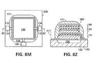
- FIGS. 8A–8Mare plan views illustrating a process for making an embodiment of an encapsulated FBAR device in accordance with the invention.
- FIGS. 8N–8Zare cross-sectional views along the section lines 8 N— 8 N through 8 Z— 8 Z, respectively, in FIGS. 8A–8M , respectively.
- FIGS. 4A and 4Bare respectively a plan view and a cross-sectional view of a first exemplary embodiment 100 of an encapsulated FBAR device in accordance with the invention.
- Encapsulated FBAR device 100comprises an FBAR stack 111 comprising FBAR 110 .
- FBAR 110is an exemplary FBAR of an FBAR ladder filter, such as that shown in FIG. 1 , or an exemplary FBAR of a duplexer.
- the remaining FBARs of such ladder filter or duplexeralso constitute part of FBAR stack 111 . However, the remaining FBARs are omitted from FIGS. 4A and 4B to simplify the drawing.
- encapsulated FBAR device 100is composed of a substrate 102 , an FBAR stack 111 over the substrate, an element that isolates the FBAR stack from the substrate, encapsulant 121 covering FBAR stack 111 , and an acoustic Bragg reflector 190 between the top surface 113 of FBAR stack 111 and encapsulant 121 .
- Acoustic Bragg reflector 190comprises a first metal Bragg layer 192 juxtaposed with a first plastic Bragg layer 194 .
- first metal Bragg layer 192is juxtaposed with encapsulant 121 and acoustic Bragg reflector 190 is additionally composed of a second metal Bragg layer 196 juxtaposed with first plastic Bragg layer 194 and a second plastic Bragg layer 198 juxtaposed with second metal Bragg layer 196 .
- Second plastic Bragg layer 198is juxtaposed with the top surface 113 of FBAR stack 111 .
- FBAR stack 111is composed of a single FBAR device 110 having opposed planar electrodes 112 and 114 and a piezoelectric element 116 between the electrodes.
- cavity 104 defined in substrate 102performs the function of acoustically isolating FBAR stack 111 from substrate 102 .
- acoustic Bragg reflector 190acoustically isolates the FBAR stack from encapsulant 121 .
- FBAR stack 111is acoustically isolated both from substrate 102 and from encapsulant 121 and is therefore free to vibrate mechanically in response to an electrical signal applied between the electrodes 112 and 114 of FBAR 110 .
- Bragg layers described in this disclosure as juxtaposedtypically physically contact one another as shown in FIG. 4B .
- juxtaposed Bragg layersmay be separated by intervening layers provided such intervening layers have a negligible effect on the acoustical properties of the juxtaposed Bragg layers.
- An element described herein as being over another elementtypically physically contacts one other element, as does remote-side electrode 114 and piezoelectric element 116 .
- an element described as over another elementmay alternatively be separated from such other element by one or more other elements.
- piezoelectric element 116may be described as being over substrate 102 , but is separated from the substrate by electrode 112 in the embodiment shown in FIG. 4B .
- the term FBAR stackrefers to a stack of layers of various materials that comprises one or more FBARs.
- the FBARsmay be at the same level in the FBAR stack or at different levels in the FBAR stack, or some of the FBARs may be at the same level in the FBAR stack and some of the FBARs may be at different levels in the FBAR stack.
- the FBARs in an FBAR ladder filterare typically at the same level in the FBAR stack
- the FBARs in a decoupled stacked bulk acoustic resonator (DSBAR)are at different levels in the FBAR stack and some of the FBARs of a thin-film acoustically-coupled transformer (FACT) are at the same level in the FBAR stack and some of the FBARs of the FACT are at different levels in the FBAR stack.
- DSBARdecoupled stacked bulk acoustic resonator
- FACTthin-film acoustically-coupled transformer
- Encapsulated FBAR device 100has a band-pass frequency response characteristic having a center frequency.
- a layer of this thicknesswill be referred to as a quarter-wave layer.
- embodiments in which at least the metal Bragg layers are thinner than quarter-wave layers, some as thin as ⁇ n /16,will give sufficient acoustic isolation for use in many applications.
- the inventorshave discovered that the acoustic isolation provided by an acoustic Bragg reflector depends on the ratio of the acoustic impedances of the materials of the Bragg layers constituting the acoustic Bragg reflector.
- the effective acoustic impedance Z eff1 presented by a first Bragg layer juxtaposed with another layeris the acoustic impedance seen at the surface of the first Bragg layer remote from the other layer.
- the effective acoustic impedance presented by the first Bragg layerdepends on the acoustic impedance of the first Bragg layer and the effective acoustic impedance presented to the first Bragg layer by the other layer.
- the effective acoustic impedance at the surface of first metal Bragg layer 192 remote from encapsulant 121depends on the acoustic impedance of the material of first metal Bragg layer 192 and the acoustic impedance of the material of the encapsulant.
- Z eff1is the effective acoustic impedance presented at the surface of first metal Bragg layer 192 remote from encapsulant 121
- Z pis the acoustic impedance of the material of first metal Bragg layer 192
- Z mis the acoustic impedance of the material of encapsulant 121 .
- Equation (1)The relationship defined by equation (1) exists between each Bragg layer and the preceding Bragg layer.
- Z mis the effective acoustic impedance presented to the Bragg layer by the preceding Bragg layer.
- first metal Bragg layer 192presents effective acoustic impedance Z eff1 to first plastic Bragg layer 194 .
- First plastic Bragg layer 194transforms the effective acoustic impedance Z eff1 to another effective acoustic impedance Z eff2 , and presents effective acoustic impedance Z eff2 to second metal Bragg layer 196 .
- Second metal Bragg layer 196transforms the effective acoustic impedance Z eff2 to another effective acoustic impedance Z eff3 , and presents effective acoustic impedance Z eff3 to second plastic Bragg layer 198 .
- Second plastic Bragg layer 198transforms the effective acoustic impedance Z eff3 to another effective acoustic impedance Z eff4 , and presents effective acoustic impedance Z eff4 to FBAR 110 .
- Effective acoustic impedance Z eff4is also the effective acoustic impedance of acoustic Bragg reflector 190 .
- the acoustic impedance mis-match between FBAR stack 111 and the effective acoustic impedance presented by acoustic Bragg reflector 190 at second plastic Bragg layer 198provides the acoustic isolation between FBAR stack 111 and encapsulant 121 .
- the effective acoustic impedances presented by Bragg layers 192 , 194 , 196 and 198respectively, alternate between high and low, the high impedance increasing and the low impedance decreasing, from first metal Bragg layer 192 to second plastic Bragg layer 198 .
- the effective acoustic impedance it presents to FBAR stack 111may be greater than or less than the acoustic impedance of the FBAR stack.
- the acoustic isolation provided by acoustic Bragg reflector 190may be quantified by the absolute value of the ratio of the effective acoustic impedance of acoustic Bragg reflector 190 and the acoustic impedance of FBAR stack 111 expressed in decibels (20 times the logarithm of the ratio). Increasing the acoustic isolation reduces the likelihood that the frequency response of FBAR device 100 will exhibit undesirable spurious artifacts due to unwanted acoustic coupling between FBAR stack 111 and encapsulant 121 .
- materials of alternate ones of the Bragg layers of acoustic Bragg reflector 190are respectively a plastic material and metal, especially a refractory metal such as tungsten or molybdenum.
- a plastic material and metalespecially a refractory metal such as tungsten or molybdenum.
- a refractory metalsuch as tungsten or molybdenum.
- the large ratio between the acoustic impedances of metals and plastic materialsenables an acoustic isolation of many tens of decibels to be obtained using relatively few Bragg layers.
- Several refractory metalsare available that have an acoustic impedance of greater than 50 Mrayl and that are compatible with the etchants used in typical FBAR fabrication processes.
- Molybdenumfor example, has an acoustic impedance of about 63 Mrayl.
- plastic materialsthat have an acoustic impedance of less than 5 Mrayl and that are compatible with the high temperatures and etchants used in typical FBAR fabrication processes.
- the acoustic impedances of some such plastic materialsare as low as about 2 Mrayl.
- Molybdenum and a crosslinked polyphenylene polymerthat will be described below have an acoustic impedance ratio of about 30.
- Plastic materials compatible with the high temperatures (>400° C.) and etchants to which first plastic Bragg layer 194 and second plastic Bragg layer 198 are subject during deposition of first metal Bragg layer 192 and second metal Bragg layer 196are available with acoustic impedances in the range from about 2 Mrayl to about 4 Mrayl.
- metalsuch as a refractory metal
- plastic material having an acoustic impedance of less than about 5 Mrayl as the material of first plastic Bragg layer 194 and second plastic Bragg layer 198result in an embodiment of acoustic Bragg reflector 190 that presents an effective acoustic impedance of about 400 rayleighs (rayl) to FBAR stack 111 .
- FBAR stack 111has an effective acoustic impedance of about 50 Mrayl, this results in an acoustic isolation of over 100 dB.
- Acoustic Bragg reflector 190provides sufficient acoustic isolation between FBAR stack 111 and encapsulant 121 for the frequency response of FBAR 110 to have a frequency response substantially free of spurious artifacts.
- Embodiments in which the plastic material has an acoustic impedance of about 2 Mraylprovide a calculated acoustic isolation of over 120 dB.
- the calculated acoustic isolation provided by gap 70 shown in FIG. 3is less than about 90 dB.
- the gas in the gaphas an acoustic impedance of about 1 krayl.
- Embodiments requiring even greater acoustic isolation between FBAR stack 111 and encapsulant 121can have additional pairs of Bragg layers of plastic and metal between first metal Bragg layer 192 and encapsulant 121 .
- the acoustic isolation provided by the illustrated embodiment of acoustic Bragg reflector 190is sufficient for most applications.
- Electrode 112 , electrode 114 and piezoelectric layer 116form a mechanical structure having a mechanical resonance that defines the center frequency of the pass-band of FBAR 110 . Electrode 112 , electrode 114 and piezoelectric element 116 are similar in thickness to the corresponding elements of a conventional FBAR whose band-pass frequency response has the same nominal center frequency. As a result, encapsulated FBAR device 100 has electrical characteristics similar to those of a similar conventional FBAR device, such as that shown in FIG. 3 , in which the top of the FBAR stack is isolated from the package by a gap.
- Encapsulated FBAR device 100additionally has a terminal pad 132 , a terminal pad 134 , an electrical trace 133 that electrically connects terminal pad 132 to electrode 112 , and an electrical trace 135 that electrically connects terminal pad 134 to electrode 114 .
- Terminal pads 132 and 134are used to make electrical connections from encapsulated FBAR device 100 to external electrical circuits (not shown).
- fabrication of the FBAR stack 111 and acoustic Bragg reflector 190 of encapsulated FBAR device 100is somewhat more complex than fabrication of the FBAR stack 56 of the conventional gap-isolated encapsulated FBAR device shown in FIG. 3 due to the need to form acoustic Bragg reflector 190 by depositing and pattering additional layers of material on the top surface 113 of FBAR stack 111 .
- FBAR device 100is encapsulated simply by covering FBAR stack 111 and acoustic Bragg reflector 190 with encapsulant material and curing the encapsulant material to form encapsulant 121 .
- the encapsulant materialis polyimide, described in more detail below.
- the encapsulant materialis a room-temperature vulcanizing rubber (RTV), a glass-loaded epoxy or another suitable encapsulant material.
- encapsulant 121may additionally comprise a thin sealing layer of metal (not shown) applied as a coating to the external surface of the cured encapsulant material. Suitable metals include aluminum and gold. The additional metal sealing layer substantially reduces the porosity of encapsulant 121 .
- FBAR stack 111may be covered by an encapsulant different from encapsulant 121 .
- a low-profile embodiment of package 54 shown in FIG. 3 in which cap 64 contacts acoustic Bragg reflector 190may provide an encapsulant covering FBAR stack 111 .
- the plastic material of the plastic Bragg layersis polyimide.
- Polyimideis sold under the trademark Kapton® by E. I. du Pont de Nemours and Company.
- plastic Bragg layers 194 and 198are each composed of polyimide applied by spin coating.
- Polyimidehas an acoustic impedance of about 4 Mrayl.
- the plastic material of the plastic Bragg layersis a poly(para-xylylene).
- plastic Bragg layers 194 and 198are each composed of poly(para-xylylene) applied by vacuum deposition.
- Poly(para-xylylene)is also known in the art as parylene.
- the dimer precursor di-para-xylylene from which parylene is made and equipment for performing vacuum deposition of layers of paryleneare available from many suppliers. Parylene has an acoustic impedance of about 2.8 Mrayl.
- the plastic material of the plastic Bragg layersis a crosslinked polyphenylene polymer.
- plastic Bragg layers 194 and 198are each composed of the crosslinked polyphenylene polymer applied by spin coating.
- Crosslinked polyphenylene polymershave been developed as low dielectric constant dielectric materials for use in integrated circuits and consequently remain stable at the high temperatures to which the crosslinked polyphenylene polymer is subject during the subsequent deposition and patterning of the metal Bragg layers of acoustic Bragg reflector 190 .
- the inventorshave discovered that crosslinked polyphenylene polymers additionally have a calculated acoustic impedance of about 2 Mrayl.
- the low acoustic impedance of crosslinked polyphenylene polymersenables embodiments of acoustic Bragg reflector 190 in which the plastic material of the plastic Bragg layers is a crosslinked polyphenylene polymer to provide an especially high acoustic isolation.
- Precursor solutions containing various oligomers that polymerize to form respective crosslinked polyphenylene polymersare sold by The Dow Chemical Company, Midland, Mich., under the trademark SiLK.
- the precursor solutionsare applied by spin coating.
- the crosslinked polyphenylene polymer obtained from one of these precursor solutions designated SiLKTM J, which additionally contains an adhesion promoter,has a calculated acoustic impedance of 2.1 Mrayl, i.e., about 2 Mrayl.
- the oligomers that polymerize to form crosslinked polyphenylene polymersare prepared from biscyclopentadienone- and aromatic acetylene-containing monomers. Using such monomers forms soluble oligomers without the need for undue substitution.
- the precursor solutioncontains a specific oligomer dissolved in gamma-butyrolactone and cyclohexanone solvents. The percentage of the oligomer in the precursor solution determines the layer thickness when the precursor solution is spun on. After application, applying heat evaporates the solvents and then cures the oligomer to form a cross-linked polymer.
- the biscyclopentadienonesreact with the acetylenes in a 4+2 cycloaddition reaction that forms a new aromatic ring. Further curing results in the cross-linked polyphenylene polymer.
- the above-described crosslinked polyphenylene polymersare disclosed by Godschalx et al. in U.S. Pat. No. 5,965,679, incorporated herein by reference. Additional practical details are described by Martin et al., Development of Low-Dielectric Constant Polymer for the Fabrication of Integrated Circuit Interconnect, 12 A DVANCED M ATERIALS , 1769 (2000), also incorporated by reference.
- crosslinked polyphenylene polymersCompared with polyimide, crosslinked polyphenylene polymers have a lower acoustic impedance, a lower acoustic attenuation and a lower dielectric constant. Moreover, a spun-on layer of the precursor solution is capable of producing a high-quality film of the crosslinked polyphenylene polymer with a thickness of the order of 200 nm, which is a typical thickness of plastic Bragg layers 194 and 198 .
- Each of the Bragg layers 192 , 194 , 196 and 198has a nominal thickness of one quarter of the wavelength in the material of the Bragg layer of an acoustic signal equal in frequency to the center frequency of the pass band of FBAR 110 .
- acoustic Bragg reflector 190presents a calculated effective acoustic impedance of about 65 rayl with polyimide plastic Bragg layers and about 4 rayl with crosslinked polyphenylene polymer plastic Bragg layers. These acoustic impedances correspond to acoustic isolations of about 118 dB and 142 dB, respectively.
- acoustic Bragg reflector 190structured to operate at about 2 GHz in which the plastic material of the plastic Bragg layers 194 and 198 is crosslinked polyphenylene polymer and the metal of the metal Bragg layers 192 and 196 is molybdenum, the thickness of the plastic Bragg layers is about 190 nm and the thickness of the metal Bragg layers is about 800 nm.
- Precursor solutions for crosslinked polyphenylene polymers formulated to spin on with a thickness of about 190 nmare commercially available. Polyimide can also be spun on in layers of this thickness. Accordingly, forming plastic Bragg layers 194 and 198 as nominal quarter-wave layers is straightforward.
- metal Bragg layers thinner than quarter-wave layers in acoustic Bragg reflector 190produces a greater proportional reduction in the acoustic isolation as the number of Bragg layers is reduced.
- better results and lower costsare typically obtained using more Bragg layers in which the metal Bragg layers are thinner than quarter-wave layers than using fewer Bragg layers in which the metal Bragg layers are quarter-wave layers.
- FIGS. 4C and 4Dare cross-sectional views of simplified examples of encapsulated FBAR device 100 in accordance with the invention in which the acoustic Bragg reflector is composed of fewer Bragg layers than acoustic Bragg reflector 190 shown in FIG. 4B .
- the encapsulated FBAR devices shown in FIGS. 4C–4Dare similar in plan view to encapsulated FBAR device 100 shown in FIG. 4A .
- second plastic Bragg layer 198( FIG. 4B ) is omitted and acoustic Bragg reflector 191 is composed of first metal Bragg layer 192 juxtaposed with first plastic Bragg layer 194 and second metal Bragg layer 196 juxtaposed with first plastic Bragg layer 194 .
- Second metal Bragg layer 196is juxtaposed with the top surface 113 of FBAR stack 111 , i.e., with electrode 114 .
- Electrode 114may be electrically isolated from second metal Bragg layer 196 by an insulating layer substantially thinner than a quarter-wave layer.
- acoustic Bragg reflector 191presents a calculated effective acoustic impedance of about 25 Grayl with polyimide plastic Bragg layers and about 99 Grayl with crosslinked polyphenylene polymer plastic Bragg layers. These acoustic impedances correspond to acoustic isolations of about 74 dB and 86 dB, respectively.
- acoustic Bragg reflector 193is composed of first metal Bragg layer 192 juxtaposed with first plastic Bragg layer 194 .
- First plastic Bragg layer 194is juxtaposed with the top surface 113 of FBAR stack 111 .
- acoustic Bragg reflector 193presents a calculated effective acoustic impedance of about 16 krayl with polyimide plastic Bragg layers and about 4 krayl with crosslinked polyphenylene polymer plastic Bragg layers. These acoustic impedances correspond to acoustic isolations of about 70 dB and 82 dB, respectively.
- FIG. 5is a cross-sectional view of a second exemplary embodiment 200 of an encapsulated FBAR device in accordance with the invention.
- Encapsulated FBAR device 200is similar in plan view to encapsulated FBAR device 100 shown in FIG. 4A .
- Encapsulated FBAR device 200comprises FBAR stack 111 comprising FBAR 110 .
- FBAR 110is an exemplary FBAR of an FBAR ladder filter, such as that shown in FIG. 1 , or an exemplary FBAR of a duplexer.
- the remaining FBARs of such ladder filter or duplexeralso constitute part of FBAR stack 111 . However, the remaining FBARs are omitted from FIG. 5 to simplify the drawing.
- Elements of encapsulated FBAR device 200 that correspond to elements of encapsulated FBAR device 100 described above with reference to FIGS. 4A and 4Bare indicated using the same reference numerals and will not be described in detail again here.
- Encapsulated FBAR device 200is composed of substrate 102 , FBAR stack 111 over the substrate, an element that isolates the FBAR stack from the substrate, encapsulant 121 covering FBAR stack 111 , and acoustic Bragg reflector 190 between the top surface 113 of FBAR stack 111 and encapsulant 121 .
- Acoustic Bragg reflector 190comprises first metal Bragg layer 192 juxtaposed with first plastic Bragg layer 194 .
- first metal Bragg layer 192 juxtaposed with encapsulant 121 and acoustic Bragg reflector 190is additionally composed of second metal Bragg layer 196 juxtaposed with first plastic Bragg layer 194 and second plastic Bragg layer 198 juxtaposed with second metal Bragg layer 196 .
- Second plastic Bragg layer 198is juxtaposed with the top surface 113 of FBAR stack 111 .
- FBAR stack 111is composed of a single FBAR device 110 having opposed planar electrodes 112 and 114 and piezoelectric element 116 between the electrodes.
- an acoustic Bragg reflector 180 located between FBAR stack 111 and substrate 102performs the functional of acoustically isolating FBAR stack 111 from substrate 102 as described in the above mentioned U.S. patent application Ser. No. 10/969,744 entitled Cavity-less Film Bulk Acoustic Resonator Devices. Additionally, acoustic Bragg reflector 190 isolates FBAR stack from encapsulant 121 as described above. Thus, FBAR stack ill is acoustically isolated from both substrate 102 and from encapsulant 121 and is therefore free to vibrate in response to an electrical signal applied between electrodes 112 and 114 of FBAR 110 .
- Acoustic Bragg reflector 180comprises a first metal Bragg layer 182 juxtaposed with a first plastic Bragg layer 184 .
- first metal Bragg layer 182is juxtaposed with the substrate and acoustic Bragg reflector 180 is additionally composed of a second metal Bragg layer 186 juxtaposed with first plastic Bragg layer 184 and a second plastic Bragg layer 188 juxtaposed with second metal Bragg layer 186 .
- metal Bragg layers 182 and 186are typically the same as those of metal Bragg layers 192 and 196 described above, although different materials may be used.
- the materials of plastic Bragg layers 184 and 188are typically the same as those of metal Bragg layers 194 and 198 described above, although different materials may be used.
- Bragg layers 182 , 184 , 186 and 188are nominally quarter-wave layers. However, similar to metal Bragg layers 192 and 196 , metal Bragg layers 182 and 186 are typically thinner than quarter-wave layers for ease of fabrication.
- acoustic Bragg reflector 180may be composed of more or fewer Bragg layers than the number exemplified in FIG. 5 . Either or both of second metal Bragg layer 186 and second plastic Bragg layer 186 may be omitted in a manner similar to that described above with reference to FIGS. 4C and 4D . Moreover, typical materials of substrate 102 have a higher acoustic impedance than encapsulant 121 so that effective acoustic isolation from substrate 102 can be obtained by reversing the order of first metal Bragg layer 182 and first plastic Bragg layer 184 to juxtapose first plastic Bragg layer 184 with substrate 102 .
- acoustic Bragg reflector 180is composed simply of first metal Bragg layer 182 and first plastic Bragg layer 184 with first plastic Bragg layer 184 juxtaposed with substrate 102 and first metal Bragg layer 182 juxtaposed with FBAR stack 111 .
- second plastic Bragg layer 186is interposed between first metal Bragg layer 182 and FBAR stack 111 .
- second plastic Bragg layer 186 and second metal Bragg layer 188are interposed in order between first metal Bragg layer 182 and FBAR stack 111 .
- encapsulated FBAR device 200does not need that a release etch be performed towards the end of the fabrication process to remove sacrificial material from cavity 104 in the substrate 102 of FBAR device 100 . Not having to perform a release etch increases the range of materials that can be used to fabricate FBAR device 200 because the materials do not have to be compatible with a release etch.
- FBAR device 200additionally has a terminal pad 132 , a terminal pad 134 , an electrical trace 133 that electrically connects terminal pad 132 to electrode 112 , and an electrical trace 135 that electrically connects terminal pad 134 to electrode 114 .
- Terminal pads 132 and 134are used to make electrical connections from FBAR device 200 to external electrical circuits (not shown).
- FIGS. 6A and 6Bare respectively a plan view and a cross-sectional view of a third exemplary embodiment 300 of an encapsulated FBAR device in accordance with the invention.
- FBAR device 300is a band-pass filter in which the FBAR stack is composed of two FBARs and an acoustic decoupler between the FBARs.
- the FBARs and the acoustic decouplerconstitute a single decoupled stacked bulk acoustic resonator (DSBAR).
- DSBARdecoupled stacked bulk acoustic resonator
- the example of FBAR device 300 shown in FIGS. 6A and 6B and described belowhas an acoustic Bragg reflector similar in structure to acoustic Bragg reflector 190 described above with reference to FIGS.
- the acoustic Bragg reflectormay alternatively be structured as described above with reference to FIGS. 4C and 4D .
- the FBAR stackis suspended over a cavity defined in the substrate to isolate the FBAR stack acoustically from the substrate.
- FBAR device 300may alternatively have an additional acoustic Bragg reflector similar to any of the embodiments of acoustic Bragg reflector 180 described above with reference to FIG. 5 between the substrate and the FBAR stack to isolate the FBAR stack acoustically from the substrate.
- FBAR device 300has a substrate 102 , an FBAR stack 311 over the substrate, an element that acoustically isolates the FBAR stack from the substrate, an encapsulant 121 covering the FBAR stack, and an acoustic Bragg reflector 190 between the top surface 313 of the FBAR stack and the encapsulant.
- FBAR stack 311is composed of lower FBAR 110 , an upper FBAR 120 stacked on lower FBAR 110 and an acoustic decoupler 130 between the FBARs.
- FBAR 110is composed of opposed planar electrodes 112 and 114 and piezoelectric element 116 between the electrodes.
- FBAR 120is composed of opposed planar electrodes 122 and 124 and a piezoelectric element 126 between the electrodes.
- Acoustic decoupler 130is located between FBARs 110 and 120 , specifically, between electrode 114 of FBAR 110 and electrode 122 of FBAR 120 .
- the acoustic decouplercontrols the coupling of acoustic energy between FBARs 110 and 120 .
- the acoustic decouplercouples less acoustic energy between the FBARs than would be coupled by direct contact between the FBARs.
- acoustic decoupler 130is composed of an acoustic decoupling layer of acoustic decoupling material.
- FBAR stack 311is suspended over cavity 104 defined in substrate 102 .
- Cavity 104performs the function of acoustically isolating FBAR stack 311 from substrate 102 .
- acoustic Bragg reflector 190is located between encapsulant 121 and the top surface 313 of FBAR stack 311 to isolate the FBAR stack acoustically from the encapsulant. The structure of acoustic Bragg reflector 190 is described above with reference to FIGS. 4A and 4B .
- the large acoustic impedance ratio between the metal of metal Bragg layers 192 and 196 and the plastic material of plastic Bragg layers 194 and 198enables acoustic Bragg reflector 190 to present a very low effective acoustic impedance to FBAR stack 311 .
- the large acoustic impedance ratio between acoustic Bragg reflector 190 and FBAR stack 311enables acoustic Bragg reflector 190 to provide sufficient acoustic isolation between FBAR stack 311 and encapsulant 121 to allow the FBARs 110 and 120 constituting DSBAR 106 to resonate mechanically in response to an input electrical signal applied between the electrodes of one of them.
- the acoustic energy generated in the FBAR that receives the input electrical signalpasses through acoustic decoupler 130 into the other FBAR.
- the FBAR receiving the acoustic energyconverts part of the acoustic energy into an electrical output signal provided between its electrodes.
- the electrical signal output between the electrodes of the FBAR receiving the acoustic energyhas a band-pass frequency response characteristic substantially free of undesirable spurious artifacts arising from undesirable acoustic coupling between FBAR stack 311 and encapsulant 121 .
- the electrodes 112 and 114 of FBAR 110are electrically connected to terminal pads 132 and 134 , respectively, by electrical traces 133 and 135 , respectively.
- the electrodes 122 and 124 of FBAR 120are electrically connected to terminal pads 134 and 138 , respectively, by electrical traces 137 and 139 .
- electrical trace 137is connected to an additional terminal pad (not shown) instead of to terminal pad 134 .
- Terminal pads 132 , 134 and 138are used to make electrical connections from FBAR device 300 to external electrical circuits (not shown).
- an acoustic decoupling layerprovides acoustic decoupler 130 .
- the acoustic decoupling layeris also a quarter-wave layer of plastic material. The same plastic material may be used in the acoustic decoupling layer and plastic Bragg layers 194 and 198 .
- the acoustic impedance of the plastic material of the acoustic decoupling layerdetermines the pass bandwidth of FBAR device 300 . The need to provide a specified pass bandwidth may result in the acoustic decoupling layer being composed of a different plastic material from plastic Bragg layers 194 and 198 .
- FIG. 7Ais a plan view of a fourth exemplary embodiment 400 of an encapsulated FBAR device in accordance with the invention.
- FBAR device 400is a film acoustically-coupled transformer (FACT) in which the FBAR stack is composed of four FBARs arranged as two decoupled stacked bulk acoustic resonators (DSBARs).
- FIGS. 7B and 7Care cross-sectional views along the section lines 7 B— 7 B and 7 C— 7 C, respectively, in FIG. 7A .
- FIG. 7Dis a schematic drawing of the electrical circuits of the example of FACT 400 shown in FIG. 7A and described below.
- acoustic Bragg reflectorsimilar in structure to acoustic Bragg reflector 190 described above with reference to FIGS. 4A and 4B located between the top surface of the FBAR stack and the encapsulant to isolate the FBAR stack acoustically from the encapsulant.
- the acoustic Bragg reflectormay alternatively be structured as described above with reference to FIGS. 4C and 4D .
- the FBAR stackis suspended over a cavity defined in the substrate to isolate the FBAR stack acoustically from the substrate.
- FBAR device 400may alternatively have an additional acoustic Bragg reflector similar to any of the embodiments of acoustic Bragg reflector 180 described above with reference to FIG. 5 between the substrate and the FBAR stack to isolate the FBAR stack acoustically from the substrate.
- FACT 400has a substrate 102 , an FBAR stack 411 over the substrate, an element that acoustically isolates the FBAR stack from the substrate, an encapsulant 121 covering the FBAR stack, and an acoustic Bragg reflector 190 between the top surface 413 of the FBAR stack and the encapsulant.
- FBAR stack 411comprises stacked bulk acoustic resonator (DSBAR) 106 and a DSBAR 108 .
- DSBAR 106is composed of lower FBAR 110 , upper FBAR 120 stacked on lower FBAR 110 and acoustic decoupler 130 between the FBARs.
- DSBAR 108is composed of a lower FBAR 150 , an upper FBAR 160 stacked on lower FBAR 150 and an acoustic decoupler 170 between the FBARs.
- FACT 400is additionally composed of an electrical circuit that interconnects the lower FBARs 110 and 150 of DSBARs 106 and 108 , respectively, and an electrical circuit that interconnects the upper FBARs 120 and 160 of DSBARs 106 and 108 , respectively.
- FIG. 7Dshows an example in which an electrical circuit 141 connects the lower FBAR 110 of DSBAR 106 and the lower FBAR 150 of DSBAR 108 in anti-parallel, and an electrical circuit 142 connects the upper FBAR 120 of DSBAR 106 and the upper FBAR 160 of DSBAR 108 in series.
- lower FBAR 110is composed of opposed planar electrodes 112 and 114 and a piezoelectric element 116 between the electrodes
- upper FBAR 120is composed of opposed planar electrodes 122 and 124 and a piezoelectric element 126 between the electrodes
- lower FBAR 150is composed of opposed planar electrodes 152 and 154 and a piezoelectric element 156 between the electrodes
- upper FBAR 160is composed of opposed planar electrodes 162 and 164 and a piezoelectric element 166 between the electrodes.
- acoustic decoupler 130 of DSBAR 106is located between lower FBAR 110 and upper FBAR 120 ; specifically, between electrode 114 of lower FBAR 110 and electrode 122 of upper FBAR 120 .
- Acoustic decoupler 130controls the coupling of acoustic energy between FBARs 110 and 120 .
- Acoustic decoupler 130couples less acoustic energy between the FBARs 110 and 120 than would be coupled if the FBARs were in direct contact with one another as they would be in a conventional stacked bulk acoustic resonator (SBAR).
- acoustic decoupler 170 of DSBAR 108is located between FBARs 150 and 160 ; specifically, between electrode 154 of lower FBAR 150 and electrode 162 of upper FBAR 160 .
- Acoustic decoupler 170controls the coupling of acoustic energy between FBARs 150 and 160 .
- Acoustic decoupler 170couples less acoustic energy between the FBARs 150 and 160 than would be coupled if the FBARs were in direct contact with one another.
- the coupling of acoustic energy defined by acoustic decouplers 130 and 170determines the pass bandwidth of FACT 400 .
- acoustic decouplers 130 and 170are respective parts of an acoustic decoupling layer 131 .
- acoustic decouplers 130 and 170are each composed of acoustic decoupling layers of acoustic decoupling materials having different acoustic impedances, as described in U.S. patent application Ser. No. 10/965,449 of John D. Larson et al., entitled Pass Bandwidth Control In Decoupled Stacked Bulk Acoustic Resonator Devices assigned to the assignee of this disclosure and incorporated by reference.
- acoustic decouplers 130 and 170are structurally independent.
- Acoustic Bragg reflector 190 located between the top surface 413 of FBAR stack 411 and encapsulant 121provides acoustic isolation between DSBARs 106 and 108 and the encapsulant.
- the structure of acoustic Bragg reflector 190is described above with reference to FIGS. 4A and 4B .
- the large acoustic impedance ratio between the metal of metal Bragg layers 192 and 196 and the plastic material of plastic Bragg layers 194 and 198enables acoustic Bragg reflector 190 to present a very high effective impedance to DSBAR 106 and DSBAR 108 .
- the large acoustic impedance ratio between acoustic Bragg reflector 190 and DSBARs 106 and 108enables acoustic Bragg reflector 190 to provide sufficient acoustic isolation between DSBARs 106 and 108 and encapsulant 121 to allow FBARs 110 and 120 to resonate mechanically in response to an input electrical signal applied between the electrodes of one of them and to allow FBARs 150 and 160 to resonate mechanically in response to an input electrical signal applied between the electrodes of one of them.
- the acoustic energy generated in the FBAR that receives the input electrical signalpasses through the respective acoustic decoupler 130 or 170 to the other FBAR.
- the FBAR receiving the acoustic energyconverts part of the acoustic energy into an electrical output signal provided between its electrodes.
- the electrical signal output between the electrodes of the FBAR receiving the acoustic energyhas a band-pass frequency response characteristic substantially free of undesirable spurious artifacts.
- FIG. 7Dschematically shows an example of the electrical circuits that interconnect DSBARs 106 and 108 and connect DSBARs 106 and 108 to external electrical circuits (not shown).
- Electrical circuit 141connects lower FBARs 110 and 150 in anti-parallel and to signal terminal 143 and ground terminal 144 .
- terminal pad 138provides signal terminal 143 and terminal pads 132 and 172 provide ground terminal 144 .
- electrical circuit 142connects upper FBARs 120 and 160 in series and to signal terminals 145 and 146 and to optional center-tap terminal 147 .
- terminal pads 134 and 174provide signal pads 145 and 146 and terminal pad 178 provides center-tap terminal 147 .
- electrical circuit 142is provided by an electrical trace 135 that extends from terminal pad 134 to electrode 124 of FBAR 120 , an electrical trace 171 that extends from electrode 122 of FBAR 120 to electrode 162 of FBAR 160 , an electrical trace 179 that extends from trace 171 to center-tap 137 , and an electrical trace 175 that extends from electrode 164 of FBAR 160 to terminal pad 174 .
- terminal pads 163 and 168interconnected by an electrical trace 169 that provide local grounds for terminal pads 134 and 174 .
- electrical trace 169additionally extends to terminal pad 178 . In other examples, terminal pad 178 is left floating.
- the electrical connections exemplified in FIG. 7Dprovide a FACT with a balanced primary and a 4:1 impedance transformation ratio or a FACT with a balanced secondary and a 1:4 impedance transformation ratio.
- the lower FBARsmay alternatively be interconnected in parallel, series, and anti-series, and the upper FBARs may alternatively be interconnected in parallel, anti-parallel and anti-series to achieve other impedance transformation ratios as shown in Table 1 below.
- the row captionsindicate the configuration of electrical circuit 141
- the column captionsindicate the configuration of electrical circuit 142
- Bdenotes that the FACT is electrically balanced
- Udenotes that the FACT is unbalanced
- Xdenotes a non-functioning FACT.
- the impedance transformation ratio shownis the impedance transformation from the configuration of electrical circuit 141 indicated by the row caption to the configuration of electrical circuit 142 indicated by the column caption.
- LOWdenotes that the FACT has a low impedance, equivalent to that of two FBARs in parallel
- HIindicates that the FACT has a high impedance, equivalent to that of two FBARs in series.
- Wafer-scale fabricationis used to fabricate thousands of FBAR devices similar to above-described FBAR devices 100 , 200 , 300 or 400 at the same time. Such wafer-scale fabrication makes the FBAR devices inexpensive to fabricate.
- An example of the fabrication method used to fabricate an embodiment of FBAR device 300 described above with reference to FIGS. 6A and 6Bwill be described next with reference to the plan views of FIGS. 8A–8M and the cross-sectional views of FIGS. 8K–8Z . With different masks, the process can also be used to fabricate embodiments of FBAR devices 100 , 200 and 400 .
- the pass band of the embodiment of FBAR device 300 whose fabrication will be describedhas a nominal center frequency of about 1.9 GHz.
- Embodiments for operation at other frequenciesare similar in structure and fabrication but have thicknesses and lateral dimensions different from those exemplified below.
- the example of FBAR device 300whose fabrication will be described below has an acoustic Bragg reflector similar in structure to acoustic Bragg reflector 190 described above with reference to FIGS. 4A and 4B .
- the described processcan be modified to deposit fewer Bragg layers to fabricate acoustic Bragg reflectors structured as described above with reference to FIGS. 4C and 4D .
- a wafer of single-crystal siliconis provided. A portion of the wafer constitutes, for each FBAR device being fabricated, a substrate corresponding to the substrate 102 of FBAR device 300 .
- FIGS. 8A–8M and FIGS. 8N–8Zillustrate and the following description describes the fabrication of FBAR device 300 in and on a portion of the wafer that constitutes substrate 102 . As FBAR device 300 is fabricated, the remaining FBAR devices on the wafer are similarly fabricated.
- FIGS. 8A and 8Nshow cavity 104 in substrate 102 filled with fill material 105 .
- the fill materialwas phosphosilicate glass (PSG) and was deposited using conventional low-pressure chemical vapor deposition (LPCVD).
- the fill materialmay alternatively be deposited by sputtering or by spin coating.
- alternating Bragg layers of metal and plasticare deposited on the surface of wafer 102 and are patterned to define an acoustic Bragg reflector similar to acoustic Bragg reflector 180 shown in FIG. 5 .
- Acoustic Bragg reflector 180 or cavity 104performs the function of acoustically isolating FBAR stack 311 ( FIG. 6B ) from substrate 102 , as described above.
- a first metal layeris deposited on the major surface of substrate 102 and fill material 105 .
- the first metal layeris patterned as shown in FIGS. 8A and 8N to define electrode 112 , terminal pad 132 , and electrical trace 133 extending between electrode 112 and terminal pad 132 .
- Electrode 112typically has an asymmetrical shape in a plane parallel to the major surface of the wafer. An asymmetrical shape minimizes lateral modes in FBAR 110 ( FIG. 6B ) of which electrode 112 forms part. This is described in U.S. Pat. No. 6,215,375 of Larson III et al., incorporated by reference. Electrode 112 leaves part of the surface of fill material 105 exposed so that the fill material can later be removed by etching, as will be described below.
- electrode 114is defined in a second metal layer
- electrode 122is defined in a third metal layer
- electrode 124is defined in a fourth metal layer, as will be described in detail below.
- the metal layers in which the electrodes are definedare patterned such that, in respective planes parallel to the major surface of the wafer, electrodes 112 and 114 of FBAR 110 have the same shape, size, orientation and position and electrodes 122 and 124 of FBAR 120 have the same shape, size, orientation and position.
- electrodes 114 and 122additionally have the same shape, size, orientation and position.
- the material of each of the metal layerswas molybdenum deposited by sputtering to a thickness of about 300 nm.
- the metal layerswere each patterned by dry etching.
- the electrodes defined in each of the metal layerswere pentagonal each with an area of about 12,000 square ⁇ m. Other electrode areas give other characteristic impedances.
- Other refractory metalssuch as tungsten, niobium and titanium may alternatively be used as the material of the metal layers.
- the metal layersmay each alternatively comprise layers of more than one material.
- the acoustic properties of the electrode materialare less important than other properties such as electrical conductivity.
- material(s) of the remaining metal parts of FBAR device 300may be different from the material of the electrodes.
- a layer of piezoelectric materialis deposited and is patterned as shown in FIGS. 8B and 8O to define piezoelectric element 116 .
- the piezoelectric layeris patterned to cover electrode 112 , but to expose terminal pad 132 and part of the surface of fill material 105 .
- Other portions of piezoelectric element 116extend over substrate 102 outside cavity 104 .
- the piezoelectric material deposited to form piezoelectric element 116 and piezoelectric element 126 described belowwas aluminum nitride and was deposited with a thickness of about 1.4 ⁇ m by sputtering.
- the piezoelectric materialwas patterned by wet etching in potassium hydroxide or by chlorine-based dry etching.
- Alternative materials for piezoelectric elements 116 and 126include zinc oxide, cadmium sulfide and poled ferroelectric materials such as perovskite ferroelectric materials, including lead zirconium titanate, lead meta niobate and barium titanate.
- the second metal layeris deposited and is patterned to define electrode 114 , terminal pad 134 and electrical trace 135 extending between electrode 114 and terminal pad 134 , as shown in FIGS. 8C and 8P . This completes fabrication of FBAR 110 .
- a layer of acoustic decoupling materialis then deposited and is patterned to define acoustic decoupler 130 , as shown in FIGS. 8D and 8Q .
- Acoustic decoupler 130is patterned to cover at least electrode 114 , and is additionally patterned to expose terminal pads 132 and 134 and part of fill material 105 .
- Acoustic decoupleris typically a third Bragg layer of plastic material.
- the acoustic decoupling material of acoustic decoupler 130was polyimide with a thickness of about 200 nm, i.e., one quarter of the center frequency wavelength in the polyimide.
- the polyimidewas deposited by spin coating, and was patterned by photolithography. Polyimide is photosensitive so that no photoresist is needed. As noted above, other plastic materials can be used as the acoustic decoupling material.
- the acoustic decoupling materialcan be deposited by methods other than spin coating.
- the waferafter depositing and patterning the polyimide, the wafer was baked initially at a temperature of about 250° C. in air and finally at a temperature of about 415° C. in an inert atmosphere, such as a nitrogen atmosphere, before further processing was performed.
- the bakeevaporates volatile constituents of the polyimide and prevents the evaporation of such volatile constituents during subsequent processing from causing separation of subsequently-deposited layers.
- the third metal layeris deposited and is patterned to define electrode 122 and electrical trace 137 extending from electrode 122 to terminal pad 134 , as shown in FIGS. 8E and 8R .
- Terminal pad 134is also electrically connected to electrode 114 by trace 135 .
- a second layer of piezoelectric materialis deposited and is patterned as shown in FIGS. 8F and 8S to define piezoelectric element 126 .
- the second piezoelectric layeris patterned to expose terminal pads 132 and 134 and part of fill material 105 .
- the fourth metal layeris deposited and is patterned to define electrode 124 , terminal pad 138 and an electrical trace 139 extending from electrode 124 to terminal pad 138 , as shown in FIGS. 8G and 8T . This completes fabrication of FBAR 120 and FBAR stack 311 .
- a gold protective layer(not shown) is deposited on the exposed surfaces of terminal pads 132 , 134 and 138 . Additionally, in embodiments in which the encapsulant is metallized as described below, an insulating layer (not shown) is deposited over each of the electrical traces 133 , 137 and 139 .
- a layer of plastic materialis deposited on the top surface 313 of FBAR stack 311 and is patterned as shown in FIGS. 8H and 8U to form second plastic Bragg layer 198 .
- the plastic material deposited to form second plastic Bragg layer 198 and first plastic Bragg layer 194 whose deposition is described belowwas polyimide.
- the polyimidewas spun on, cured and patterned to define second plastic Bragg layer 198 and first plastic Bragg layer 194 each with a thickness of about 200 nm, i.e., one quarter of the center frequency wavelength in the polyimide. Patterning polyimide is described above.
- the waferwas baked initially at a temperature of about 250° C. in air and finally at a temperature of about 415° C. in an inert atmosphere, such as a nitrogen atmosphere, before further processing was performed. The bake evaporates volatile constituents of the polyimide and prevents the evaporation of such volatile constituents during subsequent processing from causing separation of subsequently-deposited layers.
- plastic material deposited to form second plastic Bragg layer 198 and first plastic Bragg layer 194was parylene deposited by vacuum deposition from the dimer precursor di-para-xylylene.
- the plastic material deposited to form second plastic Bragg layer 198 and first plastic Bragg layer 194was a precursor solution for a crosslinked polyphenylene polymer.
- the precursor solutionwas spun, cured and patterned to define second plastic Bragg layer 198 and first plastic Bragg layer 194 each with a thickness of about 187 nm, i.e., one quarter of the center frequency wavelength in the crosslinked polyphenylene polymer. Patterning crosslinked polyphenylene polymer will be described below.
- the precursor solution for the crosslinked polyphenylene polymerwas one sold by The Dow Chemical Company and designated SiLKTM J.
- the precursor solutionmay be any suitable one of the precursor solutions now or in the future sold by The Dow Chemical Company under the trademark SiLK.
- a layer of an adhesion promoterwas deposited before the precursor solution was spun on.
- Precursor solutions containing oligomers that, when cured, form a crosslinked polyphenylene polymer having an acoustic impedance of about 2 Mraylmay be available from other suppliers now or in the future and may also be used.
- the waferwass baked at a temperature in the range from about 385° C. to about 450° C. in an inert ambient, such as under vacuum or in a nitrogen atmosphere, before further processing is performed. The bake first drives off the organic solvents from the precursor solution, and then causes the oligomer to cross link as described above to form the crosslinked polyphenylene polymer.
- a fifth metal layeris deposited on the surface of second plastic Bragg layer 184 and is patterned to define second metal Bragg layer 196 , as shown in FIGS. 8I and 8V .
- the fifth metal layer and the sixth metal layer whose deposition will be described belowwere respective layers of molybdenum each deposited to a thickness of about 800 nm by sputtering. In another embodiment with three or more Bragg layers, the thickness of the fifth metal layer and the sixth metal layer was 300 nm, as described above.
- the metal layerswere patterned by dry etching. Other refractory metals such as tungsten, niobium and titanium may alternatively be used as the material of the fifth and sixth metal layers.
- a layer of plastic materialis deposited as described above on the surface of second metal Bragg layer 196 and was patterned to define first plastic Bragg layer 194 , as shown in FIGS. 8J and 8W .
- the sixth metal layeris deposited on the surface of first plastic Bragg layer 194 , and is patterned to define first metal Bragg layer 192 , as shown in FIGS. 8K and 8X . Deposition of the sixth metal layer to form first metal Bragg layer 192 completes the fabrication of acoustic Bragg reflector 190 .
- FBAR stack 311 and acoustic Bragg reflector 190are then covered by encapsulant 121 , as shown in FIGS. 8M and 8Z .
- a drop of encapsulant materialis applied to the exposed surface of acoustic Bragg reflector 190 .
- the encapsulant materialruns off acoustic Bragg reflector to cover the top and sides of acoustic Bragg reflector 190 and FBAR stack 311 .
- the encapsulant materialis cured to form encapsulant 121 .
- the encapsulant materialis polyimide. The polyimide encapsulant material is cured as described above to form encapsulant 121 .
- the encapsulant materialis applied by injection molding.
- Alternative encapsulant materialsare a room-temperature vulcanizing rubber (RTV), a glass-loaded epoxy or another suitable encapsulant material.
- RTVroom-temperature vulcanizing rubber
- Other application techniquesare possible.
- an additional processis performed in which the cured encapsulant material is covered with a metal sealing layer (not shown) to form encapsulant 121 .
- Suitable materials of the metal sealing layerinclude aluminum and gold.
- the metal sealing layersubstantially reduces the porosity of the encapsulant.
- the metal sealing layeris patterned to expose terminal pads 132 , 134 and 138 .
- the above-described insulating layer applied to electrical traces 133 , 137 and 139 prior to the encapsulationprevents the metal sealing layer from electrically interconnecting the electrical traces.
- encapsulant 121may cover the terminal pads.
- viasextend through substrate 102 to connect terminal pads 132 , 134 and 138 to terminal pads located opposite terminal pads 132 , 134 and 138 on the surface 103 of substrate 102 .
- the waferis then divided into individual FBAR devices, including FBAR device 300 .
- FBAR device 300is mounted in a host electrical apparatus, such as a wireless telephone, and electrical connections are made between terminal pads 132 , 134 and 138 of the FBAR device and pads that are part of the host device.
- a host electrical apparatussuch as a wireless telephone
- an alternative acoustic decoupling material of acoustic decoupler 130is a crosslinked polyphenylene polymer.
- the precursor solution for the crosslinked polyphenylene polymeris spun on in a manner similar to that described above with reference to FIGS. 8D and 8Q , but is not patterned.
- the formulation of the precursor solution and the spin speedare selected so that the crosslinked polyphenylene polymer forms a layer with a thickness of about 187 nm.
- the waferis then baked as described above to cause the oligomer that forms part of the precursor solution to cross link to form the crosslinked polyphenylene polymer.
- the third metal layeris then deposited on the layer of the crosslinked polyphenylene polymer in a manner similar to that described above with reference to FIGS. 8E and 8R , but is initially patterned similarly to the patterning of acoustic decoupler 130 shown in FIG. 8D to define a hard mask that will later be used to pattern the layer of the crosslinked polyphenylene polymer to define acoustic decoupler 130 .
- the initially-patterned third metal layerhas the same extent as acoustic decoupler 130 and exposes terminal pads 132 and 134 and parts of fill material 105 .
- the layer of the crosslinked polyphenylene polymeris then patterned as shown in FIG. 8D with the initially-patterned third metal layer being used as a hard etch mask. Patterning the layer of the crosslinked polyphenylene polymer defines the extent of acoustic decoupler 130 , which exposes terminal pads 132 and 134 and parts of fill material 105 . The patterning is performed with an oxygen plasma etch.
- the third metal layeris then re-patterned as shown in FIGS. 8E and 8R to define electrode 122 and electrical trace 137 extending between electrode 122 and terminal pad 134 .
- Fabrication of the embodiment of FBAR device 300 with a layer of a crosslinked polyphenylene polymer as its acoustic decoupleris completed by performing the processing described above with reference to FIGS. 8F–8M and 8 S– 8 M.
- second plastic Bragg layer 198is a layer of a crosslinked polyphenylene polymer
- the layer of crosslinked polyphenylene polymer deposited to form second plastic Bragg layer 198is deposited, and the fifth metal layer is deposited.
- the fifth metal layeris then initially patterned to define second plastic Bragg layer 198
- the layer of the crosslinked polyphenylene polymeris patterned using the initially-patterned fifth metal layer as a hard etch mask, and the fifth metal layer is then re-patterned to define second metal Bragg layer 196 .
- the initial patterning of the fifth metal layerdefines second metal Bragg layer 196 , and the above-described re-patterning of the fifth metal layer is omitted.
- a similar techniquecan be used to define second plastic Bragg layer 198 in a layer of parylene.
- first plastic Bragg layer 194is a layer of a crosslinked polyphenylene polymer
- the layer of crosslinked polyphenylene polymer deposited to form first plastic Bragg layer 194is deposited, and the sixth metal layer is deposited.
- the sixth metal layeris then initially patterned to define first plastic Bragg layer 194
- the layer of the crosslinked polyphenylene polymeris patterned using the initially-patterned sixth metal layer as a hard etch mask, and the sixth metal layer is then re-patterned to define first metal Bragg layer 192 .
- first metal Bragg layer 194is a layer of a crosslinked polyphenylene polymer
- first plastic Bragg layer 192in which the first plastic Bragg layer and the first metal Bragg layer have the same extent, the initial patterning of the sixth metal layer defines first metal Bragg layer 192 , and the above-described re-patterning of the sixth metal layer is omitted.
- a similar techniquecan be used to define first plastic Bragg layer 196 in a layer of parylene.
Landscapes
- Physics & Mathematics (AREA)
- Acoustics & Sound (AREA)
- Chemical & Material Sciences (AREA)
- Crystallography & Structural Chemistry (AREA)
- Piezo-Electric Or Mechanical Vibrators, Or Delay Or Filter Circuits (AREA)
Abstract
Description
Zeff1=Zp2/Zm (1)
where Zpis the acoustic impedance of the material of the first Bragg layer and Zmis the acoustic impedance of the other layer.
| TABLE 1 | |||||
| Parallel | Series | Anti-parallel. | Anti-series | ||
| Parallel | U 1:1 LOW | X | X | U 1:4 |
| Series | X | B 1:1 HI | B 4:1 | X |
| Anti-parallel. | X | B 1:4 | B 1:1 LOW | X |
| Anti-series | U 4:1 | X | X | U 1:1 HI |
Claims (21)
Priority Applications (1)
| Application Number | Priority Date | Filing Date | Title |
|---|---|---|---|
| US10/969,636US7358831B2 (en) | 2003-10-30 | 2004-10-19 | Film bulk acoustic resonator (FBAR) devices with simplified packaging |
Applications Claiming Priority (5)
| Application Number | Priority Date | Filing Date | Title |
|---|---|---|---|
| US10/699,481US6946928B2 (en) | 2003-10-30 | 2003-10-30 | Thin-film acoustically-coupled transformer |
| US10/699,289US7019605B2 (en) | 2003-10-30 | 2003-10-30 | Stacked bulk acoustic resonator band-pass filter with controllable pass bandwidth |
| US10/965,637US7391285B2 (en) | 2003-10-30 | 2004-10-13 | Film acoustically-coupled transformer |
| US10/965,541US7400217B2 (en) | 2003-10-30 | 2004-10-13 | Decoupled stacked bulk acoustic resonator band-pass filter with controllable pass bandwith |
| US10/969,636US7358831B2 (en) | 2003-10-30 | 2004-10-19 | Film bulk acoustic resonator (FBAR) devices with simplified packaging |
Related Parent Applications (2)
| Application Number | Title | Priority Date | Filing Date |
|---|---|---|---|
| US10/699,289Continuation-In-PartUS7019605B2 (en) | 2003-10-30 | 2003-10-30 | Stacked bulk acoustic resonator band-pass filter with controllable pass bandwidth |
| US10/699,481Continuation-In-PartUS6946928B2 (en) | 2003-10-30 | 2003-10-30 | Thin-film acoustically-coupled transformer |
Publications (2)
| Publication Number | Publication Date |
|---|---|
| US20050110597A1 US20050110597A1 (en) | 2005-05-26 |
| US7358831B2true US7358831B2 (en) | 2008-04-15 |
Family
ID=34557693
Family Applications (2)
| Application Number | Title | Priority Date | Filing Date |
|---|---|---|---|
| US10/969,636Expired - LifetimeUS7358831B2 (en) | 2003-10-30 | 2004-10-19 | Film bulk acoustic resonator (FBAR) devices with simplified packaging |
| US10/969,744Expired - LifetimeUS7332985B2 (en) | 2003-10-30 | 2004-10-19 | Cavity-less film bulk acoustic resonator (FBAR) devices |
Family Applications After (1)
| Application Number | Title | Priority Date | Filing Date |
|---|---|---|---|
| US10/969,744Expired - LifetimeUS7332985B2 (en) | 2003-10-30 | 2004-10-19 | Cavity-less film bulk acoustic resonator (FBAR) devices |
Country Status (5)
| Country | Link |
|---|---|
| US (2) | US7358831B2 (en) |
| JP (2) | JP2007514341A (en) |
| DE (2) | DE112004002004B4 (en) |
| GB (3) | GB2423428B (en) |
| WO (3) | WO2005043751A1 (en) |
Cited By (113)
| Publication number | Priority date | Publication date | Assignee | Title |
|---|---|---|---|---|
| US20070024395A1 (en)* | 2005-07-28 | 2007-02-01 | Kabushiki Kaisha Toshiba | Film bulk acoustic resonator, filter circuit and method for manufacturing a film bulk acoustic resonator |
| US20080078233A1 (en)* | 2006-09-25 | 2008-04-03 | Larson John D | Apparatus and method for measuring an environmental condition |
| US20080168638A1 (en)* | 2007-01-17 | 2008-07-17 | Rf Micro Devices, Inc. | Piezoelectric substrate for a saw device |
| US20090045704A1 (en)* | 2007-08-14 | 2009-02-19 | Skyworks Solutions, Inc. | Method for forming a multi-layer electrode underlying a piezoelectric layer and related structure |
| US7619347B1 (en)* | 2005-05-24 | 2009-11-17 | Rf Micro Devices, Inc. | Layer acoustic wave device and method of making the same |
| US7737612B1 (en)* | 2005-05-25 | 2010-06-15 | Maxim Integrated Products, Inc. | BAW resonator bi-layer top electrode with zero etch undercut |
| US20100187948A1 (en)* | 2009-01-26 | 2010-07-29 | Resonance Semiconductor Corporation | Protected resonator |
| US20100212127A1 (en)* | 2009-02-24 | 2010-08-26 | Habbo Heinze | Process for Adapting Resonance Frequency of a BAW Resonator |
| US20100277257A1 (en)* | 2004-12-22 | 2010-11-04 | Avago Technologies Wireless Ip (Singapore) Pte. Ltd. | Acoustic resonator performance enhancement using selective metal etch |
| US20110121916A1 (en)* | 2009-11-24 | 2011-05-26 | Avago Technologies Wireless Ip (Singapore) Pte. Ltd. | Hybrid bulk acoustic wave resonator |
| US20110304412A1 (en)* | 2010-06-10 | 2011-12-15 | Hao Zhang | Acoustic Wave Resonators and Methods of Manufacturing Same |
| US20120056694A1 (en)* | 2010-09-07 | 2012-03-08 | Wei Pang | Composite bulk acoustic wave resonator |
| CN102571027A (en)* | 2012-02-27 | 2012-07-11 | 浙江瑞能通信科技有限公司 | Film bulk acoustic resonator structure based on all metal Bragg reflection layer |
| US20120200195A1 (en)* | 2009-09-28 | 2012-08-09 | Taiyo Yuden Co., Ltd. | Acoustic wave device |
| US8248185B2 (en) | 2009-06-24 | 2012-08-21 | Avago Technologies Wireless Ip (Singapore) Pte. Ltd. | Acoustic resonator structure comprising a bridge |
| WO2012147038A1 (en)* | 2011-04-28 | 2012-11-01 | Lam Research Ag | Improved ultrasonic treatment method and apparatus |
| US8330325B1 (en) | 2011-06-16 | 2012-12-11 | Avago Technologies Wireless Ip (Singapore) Pte. Ltd. | Bulk acoustic resonator comprising non-piezoelectric layer |
| US8350445B1 (en) | 2011-06-16 | 2013-01-08 | Avago Technologies Wireless Ip (Singapore) Pte. Ltd. | Bulk acoustic resonator comprising non-piezoelectric layer and bridge |
| US8357981B2 (en) | 2010-05-28 | 2013-01-22 | Avago Technologies Wireless Ip (Singapore) Pte. Ltd. | Transducer devices having different frequencies based on layer thicknesses and method of fabricating the same |
| DE102012214323A1 (en) | 2011-08-12 | 2013-02-14 | Avago Technologies Wireless Ip (Singapore) Pte. Ltd. | Bulk acoustic wave (BAW) resonator used in electrical filter, has electrodes that are respectively located over piezoelectric layer, and bridge that is positioned between electrodes |
| US20130049545A1 (en)* | 2010-04-29 | 2013-02-28 | Avago Technologies General Ip (Singapore) Pte. Ltd. | Resonator device including electrodes with buried temperature compensating layers |
| US8436516B2 (en) | 2010-04-29 | 2013-05-07 | Avago Technologies General Ip (Singapore) Pte. Ltd. | Resonator device including electrode with buried temperature compensating layer |
| DE102012224460A1 (en) | 2011-12-27 | 2013-06-27 | Avago Technologies Wireless Ip (Singapore) Pte. Ltd. | Solid-mount bulk acoustic wave resonator (SMR) used in wireless communication device, has active area of acoustic reflector that is formed by overlapping of acoustic reflector, electrodes and piezoelectric layer |
| US8490260B1 (en) | 2007-01-17 | 2013-07-23 | Rf Micro Devices, Inc. | Method of manufacturing SAW device substrates |
| US8522411B1 (en) | 2007-01-16 | 2013-09-03 | Triquint Semiconductor, Inc. | Method to control BAW resonator top electrode edge during patterning |
| US8575820B2 (en) | 2011-03-29 | 2013-11-05 | Avago Technologies General Ip (Singapore) Pte. Ltd. | Stacked bulk acoustic resonator |
| US20130320808A1 (en)* | 2012-05-31 | 2013-12-05 | Texas Instruments Incorporated | Integrated resonator with a mass bias |
| DE102013221449A1 (en) | 2012-10-23 | 2014-04-24 | Avago Technologies General Ip (Singapore) Pte. Ltd. | An acoustic resonator with a guard ring |
| DE102013221030A1 (en) | 2012-10-18 | 2014-04-24 | Avago Technologies General Ip (Singapore) Pte. Ltd. | Bulk acoustic wave (BAW) resonator device for cellular telephone, has bridge that is formed within acoustic impedance layers of acoustic reflector and resonator stack, and piezoelectric layer that is formed over bottom electrode |
| US8796904B2 (en) | 2011-10-31 | 2014-08-05 | Avago Technologies General Ip (Singapore) Pte. Ltd. | Bulk acoustic resonator comprising piezoelectric layer and inverse piezoelectric layer |
| DE102014101805A1 (en) | 2013-02-14 | 2014-08-28 | Avago Technologies General Ip (Singapore) Pte. Ltd. | Bulk acoustic wave resonator device e.g. thin film bulk acoustic resonator device, for ladder filter for e.g. laptops, has compensation layer including positive temperature coefficient for offsetting portion of negative coefficient |
| US8872604B2 (en) | 2011-05-05 | 2014-10-28 | Avago Technologies General Ip (Singapore) Pte. Ltd. | Double film bulk acoustic resonators with electrode layer and piezo-electric layer thicknesses providing improved quality factor |
| US8896395B2 (en) | 2011-09-14 | 2014-11-25 | Avago Technologies General Ip (Singapore) Pte. Ltd. | Accoustic resonator having multiple lateral features |
| US8902023B2 (en) | 2009-06-24 | 2014-12-02 | Avago Technologies General Ip (Singapore) Pte. Ltd. | Acoustic resonator structure having an electrode with a cantilevered portion |
| US8922302B2 (en) | 2011-08-24 | 2014-12-30 | Avago Technologies General Ip (Singapore) Pte. Ltd. | Acoustic resonator formed on a pedestal |
| US8962443B2 (en) | 2011-01-31 | 2015-02-24 | Avago Technologies General Ip (Singapore) Pte. Ltd. | Semiconductor device having an airbridge and method of fabricating the same |
| US8981876B2 (en) | 2004-11-15 | 2015-03-17 | Avago Technologies General Ip (Singapore) Pte. Ltd. | Piezoelectric resonator structures and electrical filters having frame elements |
| US9048812B2 (en) | 2011-02-28 | 2015-06-02 | Avago Technologies General Ip (Singapore) Pte. Ltd. | Bulk acoustic wave resonator comprising bridge formed within piezoelectric layer |
| US20150171822A1 (en)* | 2012-08-03 | 2015-06-18 | Epcos Ag | Topographical structure and method of producing it |
| US9083302B2 (en) | 2011-02-28 | 2015-07-14 | Avago Technologies General Ip (Singapore) Pte. Ltd. | Stacked bulk acoustic resonator comprising a bridge and an acoustic reflector along a perimeter of the resonator |
| US9088265B2 (en) | 2013-05-17 | 2015-07-21 | Avago Technologies General Ip (Singapore) Pte. Ltd. | Bulk acoustic wave resonator comprising a boron nitride piezoelectric layer |
| US9099983B2 (en) | 2011-02-28 | 2015-08-04 | Avago Technologies General Ip (Singapore) Pte. Ltd. | Bulk acoustic wave resonator device comprising a bridge in an acoustic reflector |
| US9136818B2 (en) | 2011-02-28 | 2015-09-15 | Avago Technologies General Ip (Singapore) Pte. Ltd. | Stacked acoustic resonator comprising a bridge |
| US9136819B2 (en) | 2012-10-27 | 2015-09-15 | Avago Technologies General Ip (Singapore) Pte. Ltd. | Bulk acoustic wave resonator having piezoelectric layer with multiple dopants |
| US9148117B2 (en) | 2011-02-28 | 2015-09-29 | Avago Technologies General Ip (Singapore) Pte. Ltd. | Coupled resonator filter comprising a bridge and frame elements |
| DE102014105951A1 (en) | 2014-03-26 | 2015-10-01 | Avago Technologies General Ip (Singapore) Pte. Ltd. | Acoustic resonator with a planarization layer and a method for producing the same |
| DE102014105950A1 (en) | 2014-03-28 | 2015-10-01 | Avago Technologies General Ip (Singapore) Pte. Ltd. | A trench acoustic resonator device for providing stress relief |
| US9154112B2 (en) | 2011-02-28 | 2015-10-06 | Avago Technologies General Ip (Singapore) Pte. Ltd. | Coupled resonator filter comprising a bridge |
| US9154111B2 (en) | 2011-05-20 | 2015-10-06 | Avago Technologies General Ip (Singapore) Pte. Ltd. | Double bulk acoustic resonator comprising aluminum scandium nitride |
| DE102015106724A1 (en) | 2014-04-30 | 2015-11-05 | Avago Technologies General Ip (Singapore) Pte. Ltd. | Acoustic resonator device with an airfoil and a temperature-compensating layer |
| US9203374B2 (en) | 2011-02-28 | 2015-12-01 | Avago Technologies General Ip (Singapore) Pte. Ltd. | Film bulk acoustic resonator comprising a bridge |
| DE102015108517A1 (en) | 2014-05-29 | 2015-12-03 | Avago Technologies General Ip (Singapore) Pte. Ltd. | Capacitively coupled resonator device with air gap separating electrode and piezoelectric layer |
| DE102015108508A1 (en) | 2014-05-30 | 2015-12-03 | Avago Technologies General Ip (Singapore) Pte. Ltd. | Acoustic resonator with vertically extended acoustic cavity |
| US9219464B2 (en) | 2009-11-25 | 2015-12-22 | Avago Technologies General Ip (Singapore) Pte. Ltd. | Bulk acoustic wave (BAW) resonator structure having an electrode with a cantilevered portion and a piezoelectric layer with multiple dopants |
| US9225313B2 (en) | 2012-10-27 | 2015-12-29 | Avago Technologies General Ip (Singapore) Pte. Ltd. | Bulk acoustic wave resonator having doped piezoelectric layer with improved piezoelectric characteristics |
| US9227839B2 (en)* | 2014-05-06 | 2016-01-05 | Raytheon Company | Wafer level packaged infrared (IR) focal plane array (FPA) with evanescent wave coupling |
| US9243316B2 (en) | 2010-01-22 | 2016-01-26 | Avago Technologies General Ip (Singapore) Pte. Ltd. | Method of fabricating piezoelectric material with selected c-axis orientation |
| US9246473B2 (en) | 2011-03-29 | 2016-01-26 | Avago Technologies General Ip (Singapore) Pte. Ltd. | Acoustic resonator comprising collar, frame and perimeter distributed bragg reflector |
| DE102015117953A1 (en) | 2014-10-22 | 2016-04-28 | Avago Technologies General Ip (Singapore) Pte. Ltd. | A bulk acoustic wave resonator device comprising a temperature compensation device having a layer of low acoustic impedance |
| DE102015118594A1 (en) | 2014-10-31 | 2016-05-04 | Avago Technologies General Ip (Singapore) Pte. Ltd. | A packaged device comprising a cavity package having an elastic layer within a molding compound |
| US20160191015A1 (en)* | 2014-12-27 | 2016-06-30 | Avago Technologies General Ip (Singapore) Pte. Ltd. | Split current bulk acoustic wave (baw) resonators |
| US9401692B2 (en) | 2012-10-29 | 2016-07-26 | Avago Technologies General Ip (Singapore) Pte. Ltd. | Acoustic resonator having collar structure |
| US9425764B2 (en) | 2012-10-25 | 2016-08-23 | Avago Technologies General Ip (Singapore) Pte. Ltd. | Accoustic resonator having composite electrodes with integrated lateral features |
| US9444426B2 (en) | 2012-10-25 | 2016-09-13 | Avago Technologies General Ip (Singapore) Pte. Ltd. | Accoustic resonator having integrated lateral feature and temperature compensation feature |
| US9450167B2 (en) | 2013-03-28 | 2016-09-20 | Avago Technologies General Ip (Singapore) Pte. Ltd. | Temperature compensated acoustic resonator device having an interlayer |
| US9450561B2 (en) | 2009-11-25 | 2016-09-20 | Avago Technologies General Ip (Singapore) Pte. Ltd. | Bulk acoustic wave (BAW) resonator structure having an electrode with a cantilevered portion and a piezoelectric layer with varying amounts of dopant |
| US9455681B2 (en) | 2014-02-27 | 2016-09-27 | Avago Technologies General Ip (Singapore) Pte. Ltd. | Bulk acoustic wave resonator having doped piezoelectric layer |
| US9490770B2 (en) | 2011-03-29 | 2016-11-08 | Avago Technologies General Ip (Singapore) Pte. Ltd. | Acoustic resonator comprising temperature compensating layer and perimeter distributed bragg reflector |
| US9490418B2 (en) | 2011-03-29 | 2016-11-08 | Avago Technologies General Ip (Singapore) Pte. Ltd. | Acoustic resonator comprising collar and acoustic reflector with temperature compensating layer |
| US9490771B2 (en) | 2012-10-29 | 2016-11-08 | Avago Technologies General Ip (Singapore) Pte. Ltd. | Acoustic resonator comprising collar and frame |
| US9520856B2 (en) | 2009-06-24 | 2016-12-13 | Avago Technologies General Ip (Singapore) Pte. Ltd. | Acoustic resonator structure having an electrode with a cantilevered portion |
| US9525397B2 (en) | 2011-03-29 | 2016-12-20 | Avago Technologies General Ip (Singapore) Pte. Ltd. | Acoustic resonator comprising acoustic reflector, frame and collar |
| US9571064B2 (en) | 2011-02-28 | 2017-02-14 | Avago Technologies General Ip (Singapore) Pte. Ltd. | Acoustic resonator device with at least one air-ring and frame |
| US9571063B2 (en) | 2014-10-28 | 2017-02-14 | Avago Technologies General Ip (Singapore) Pte. Ltd. | Acoustic resonator device with structures having different apodized shapes |
| US9577603B2 (en) | 2011-09-14 | 2017-02-21 | Avago Technologies General Ip (Singapore) Pte. Ltd. | Solidly mounted acoustic resonator having multiple lateral features |
| US9590165B2 (en) | 2011-03-29 | 2017-03-07 | Avago Technologies General Ip (Singapore) Pte. Ltd. | Acoustic resonator comprising aluminum scandium nitride and temperature compensation feature |
| US9602073B2 (en) | 2013-05-31 | 2017-03-21 | Avago Technologies General Ip (Singapore) Pte. Ltd. | Bulk acoustic wave resonator having piezoelectric layer with varying amounts of dopant |
| US9608592B2 (en) | 2014-01-21 | 2017-03-28 | Avago Technologies General Ip (Singapore) Pte. Ltd. | Film bulk acoustic wave resonator (FBAR) having stress-relief |
| US9608192B2 (en) | 2013-03-28 | 2017-03-28 | Avago Technologies General Ip (Singapore) Pte. Ltd. | Temperature compensated acoustic resonator device |
| US9608589B2 (en) | 2010-10-26 | 2017-03-28 | Avago Technologies General Ip (Singapore) Pte. Ltd. | Method of forming acoustic resonator using intervening seed layer |
| US9673778B2 (en) | 2009-06-24 | 2017-06-06 | Avago Technologies General Ip (Singapore) Pte. Ltd. | Solid mount bulk acoustic wave resonator structure comprising a bridge |
| US9679765B2 (en) | 2010-01-22 | 2017-06-13 | Avago Technologies General Ip (Singapore) Pte. Ltd. | Method of fabricating rare-earth doped piezoelectric material with various amounts of dopants and a selected C-axis orientation |
| US9691963B2 (en) | 2014-05-29 | 2017-06-27 | Avago Technologies General Ip (Singapore) Pte. Ltd. | Capacitive coupled resonator and filter device with comb electrodes and support pillars separating piezoelectric layer |
| US9698754B2 (en) | 2014-05-29 | 2017-07-04 | Avago Technologies General Ip (Singapore) Pte. Ltd. | Capacitive coupled resonator and filter device with comb electrodes and support frame separation from piezoelectric layer |
| US9735338B2 (en) | 2009-01-26 | 2017-08-15 | Cymatics Laboratories Corp. | Protected resonator |
| US9748918B2 (en) | 2013-02-14 | 2017-08-29 | Avago Technologies General Ip (Singapore) Pte. Ltd. | Acoustic resonator comprising integrated structures for improved performance |
| DE102017106582A1 (en) | 2016-03-29 | 2017-10-05 | Avago Technologies General Ip (Singapore) Pte. Ltd. | Temperature-compensated acoustic resonator device with thin intermediate seed layer |
| DE102017106584A1 (en) | 2016-03-31 | 2017-10-05 | Avago Technologies General Ip (Singapore) Pte. Ltd. | Acoustic resonator including monolithic piezoelectric layer of opposite polarities |
| DE102017108340A1 (en) | 2016-04-21 | 2017-10-26 | Avago Technologies General Ip (Singapore) Pte. Ltd. | Bulk Acoustic Wave (BAW) resonator structure |
| WO2017191499A1 (en) | 2016-05-06 | 2017-11-09 | Waseda University | Piezoelectric layer and piezoelectric device comprising the piezoelectric layer |
| US9853626B2 (en) | 2014-03-31 | 2017-12-26 | Avago Technologies General Ip (Singapore) Pte. Ltd. | Acoustic resonator comprising acoustic redistribution layers and lateral features |
| US9917567B2 (en) | 2011-05-20 | 2018-03-13 | Avago Technologies General Ip (Singapore) Pte. Ltd. | Bulk acoustic resonator comprising aluminum scandium nitride |
| US9991871B2 (en) | 2011-02-28 | 2018-06-05 | Avago Technologies General Ip (Singapore) Pte. Ltd. | Bulk acoustic wave resonator comprising a ring |
| DE102018107674A1 (en) | 2017-03-31 | 2018-10-04 | Avago Technologies General Ip (Singapore) Pte. Ltd. | Acoustic resonator with extended cavity |
| US10164605B2 (en) | 2016-01-26 | 2018-12-25 | Avago Technologies International Sales Pte. Limited | Bulk acoustic wave resonator with piezoelectric layer comprising lithium niobate or lithium tantalate |
| US10263601B2 (en) | 2016-10-31 | 2019-04-16 | Avago Technologies International Sales Pte. Limited | Tunable bulk acoustic resonator device with improved insertion loss |
| US10263587B2 (en) | 2016-12-23 | 2019-04-16 | Avago Technologies International Sales Pte. Limited | Packaged resonator with polymeric air cavity package |
| US10284168B2 (en) | 2016-10-27 | 2019-05-07 | Avago Technologies International Sales Pte. Limited | Bulk acoustic wave resonator |
| US10340885B2 (en) | 2014-05-08 | 2019-07-02 | Avago Technologies International Sales Pte. Limited | Bulk acoustic wave devices with temperature-compensating niobium alloy electrodes |
| US10367472B2 (en) | 2012-10-25 | 2019-07-30 | Avago Technologies International Sales Pte. Limited | Acoustic resonator having integrated lateral feature and temperature compensation feature |
| US10404231B2 (en) | 2014-02-27 | 2019-09-03 | Avago Technologies International Sales Pte. Limited | Acoustic resonator device with an electrically-isolated layer of high-acoustic-impedance material interposed therein |
| US10511285B1 (en) | 2017-02-28 | 2019-12-17 | Avago Technologies International Sales Pte. Limited | Anchored polymeric package for acoustic resonator structures |
| US20200083861A1 (en)* | 2018-09-12 | 2020-03-12 | Skyworks Global Pte. Ltd. | Recess frame structure for a bulk acoustic wave resonator |
| CN111030634A (en)* | 2019-12-31 | 2020-04-17 | 诺思(天津)微系统有限责任公司 | Bulk acoustic wave resonator with electrical isolation layer and its manufacturing method, filter and electronic equipment |
| US10700660B2 (en) | 2017-10-25 | 2020-06-30 | Avago Technologies International Sales Pte. Limited | Bulk acoustic wave resonator |
| US10804877B2 (en) | 2014-01-21 | 2020-10-13 | Avago Technologies International Sales Pte. Limited | Film bulk acoustic wave resonator (FBAR) having stress-relief |
| US10804875B2 (en) | 2017-09-29 | 2020-10-13 | Avago Technologies International Sales Pte. Limited | Polymer lid wafer-level package with an electrically and thermally conductive pillar |
| US10886888B2 (en) | 2016-10-27 | 2021-01-05 | Avago Technologies International Sales Pte. Limited | Bulk acoustic wave resonator having openings in an active area and a pillar beneath the opening |
| US11018651B2 (en) | 2018-04-19 | 2021-05-25 | Avago Technologies International Sales Pte. Limited | Bulk acoustic wave resonators having doped piezoelectric material and an adhesion and diffusion barrier layer |
| US11152909B2 (en) | 2018-04-19 | 2021-10-19 | Avago Technologies International Sales Pte. Limited | Bulk acoustic wave resonators having low atomic weight metal electrodes |
| US20230023845A1 (en)* | 2014-06-06 | 2023-01-26 | Akoustis, Inc. | Method of manufacture for single crystal capacitor dielectric for a resonance circuit |
| US12334906B2 (en) | 2021-12-30 | 2025-06-17 | Raytheon Company | Multi-layer resonator assembly and method for fabricating same |
| US12334908B2 (en) | 2021-12-10 | 2025-06-17 | Skyworks Solutions, Inc. | Bulk acoustic wave filters for improving noise factor |
Families Citing this family (105)
| Publication number | Priority date | Publication date | Assignee | Title |
|---|---|---|---|---|
| US6050943A (en) | 1997-10-14 | 2000-04-18 | Guided Therapy Systems, Inc. | Imaging, therapy, and temperature monitoring ultrasonic system |
| US7275292B2 (en) | 2003-03-07 | 2007-10-02 | Avago Technologies Wireless Ip (Singapore) Pte. Ltd. | Method for fabricating an acoustical resonator on a substrate |
| US7362198B2 (en)* | 2003-10-30 | 2008-04-22 | Avago Technologies Wireless Ip (Singapore) Pte. Ltd | Pass bandwidth control in decoupled stacked bulk acoustic resonator devices |
| US6946928B2 (en)* | 2003-10-30 | 2005-09-20 | Agilent Technologies, Inc. | Thin-film acoustically-coupled transformer |
| US7242270B2 (en)* | 2003-10-30 | 2007-07-10 | Avago Technologies Wireless Ip (Singapore) Pte. Ltd. | Decoupled stacked bulk acoustic resonator-based band-pass filter |
| EP1528677B1 (en)* | 2003-10-30 | 2006-05-10 | Agilent Technologies, Inc. | Film acoustically-coupled transformer with two reverse c-axis piezoelectric elements |
| US7358831B2 (en)* | 2003-10-30 | 2008-04-15 | Avago Technologies Wireless Ip (Singapore) Pte. Ltd. | Film bulk acoustic resonator (FBAR) devices with simplified packaging |
| US7019605B2 (en)* | 2003-10-30 | 2006-03-28 | Larson Iii John D | Stacked bulk acoustic resonator band-pass filter with controllable pass bandwidth |
| US7615833B2 (en) | 2004-07-13 | 2009-11-10 | Avago Technologies Wireless Ip (Singapore) Pte. Ltd. | Film bulk acoustic resonator package and method of fabricating same |
| DE102004035812A1 (en)* | 2004-07-23 | 2006-03-16 | Epcos Ag | Resonant bulk acoustic wave resonator |
| US7393325B2 (en) | 2004-09-16 | 2008-07-01 | Guided Therapy Systems, L.L.C. | Method and system for ultrasound treatment with a multi-directional transducer |
| US9011336B2 (en) | 2004-09-16 | 2015-04-21 | Guided Therapy Systems, Llc | Method and system for combined energy therapy profile |
| US7824348B2 (en) | 2004-09-16 | 2010-11-02 | Guided Therapy Systems, L.L.C. | System and method for variable depth ultrasound treatment |
| US20120165848A1 (en) | 2010-08-02 | 2012-06-28 | Guided Therapy Systems, Llc | System and method for treating cartilage |
| US10864385B2 (en) | 2004-09-24 | 2020-12-15 | Guided Therapy Systems, Llc | Rejuvenating skin by heating tissue for cosmetic treatment of the face and body |
| US8444562B2 (en) | 2004-10-06 | 2013-05-21 | Guided Therapy Systems, Llc | System and method for treating muscle, tendon, ligament and cartilage tissue |
| US8535228B2 (en) | 2004-10-06 | 2013-09-17 | Guided Therapy Systems, Llc | Method and system for noninvasive face lifts and deep tissue tightening |
| US7388454B2 (en) | 2004-10-01 | 2008-06-17 | Avago Technologies Wireless Ip Pte Ltd | Acoustic resonator performance enhancement using alternating frame structure |
| US7758524B2 (en) | 2004-10-06 | 2010-07-20 | Guided Therapy Systems, L.L.C. | Method and system for ultra-high frequency ultrasound treatment |
| US11235179B2 (en) | 2004-10-06 | 2022-02-01 | Guided Therapy Systems, Llc | Energy based skin gland treatment |
| JP2008522642A (en) | 2004-10-06 | 2008-07-03 | ガイデッド セラピー システムズ, エル.エル.シー. | Method and system for beauty enhancement |
| US9694212B2 (en) | 2004-10-06 | 2017-07-04 | Guided Therapy Systems, Llc | Method and system for ultrasound treatment of skin |
| US11883688B2 (en) | 2004-10-06 | 2024-01-30 | Guided Therapy Systems, Llc | Energy based fat reduction |
| US9827449B2 (en) | 2004-10-06 | 2017-11-28 | Guided Therapy Systems, L.L.C. | Systems for treating skin laxity |
| JP5094402B2 (en) | 2004-10-06 | 2012-12-12 | ガイデッド セラピー システムズ, エル.エル.シー. | Method and system for ultrasonic tissue processing |
| US8133180B2 (en) | 2004-10-06 | 2012-03-13 | Guided Therapy Systems, L.L.C. | Method and system for treating cellulite |
| US20060111744A1 (en) | 2004-10-13 | 2006-05-25 | Guided Therapy Systems, L.L.C. | Method and system for treatment of sweat glands |
| US8690779B2 (en) | 2004-10-06 | 2014-04-08 | Guided Therapy Systems, Llc | Noninvasive aesthetic treatment for tightening tissue |
| US11724133B2 (en) | 2004-10-07 | 2023-08-15 | Guided Therapy Systems, Llc | Ultrasound probe for treatment of skin |
| US11207548B2 (en) | 2004-10-07 | 2021-12-28 | Guided Therapy Systems, L.L.C. | Ultrasound probe for treating skin laxity |
| US7202560B2 (en) | 2004-12-15 | 2007-04-10 | Avago Technologies Wireless Ip (Singapore) Pte. Ltd. | Wafer bonding of micro-electro mechanical systems to active circuitry |
| US7427819B2 (en)* | 2005-03-04 | 2008-09-23 | Avago Wireless Ip Pte Ltd | Film-bulk acoustic wave resonator with motion plate and method |
| US7369013B2 (en)* | 2005-04-06 | 2008-05-06 | Avago Technologies Wireless Ip Pte Ltd | Acoustic resonator performance enhancement using filled recessed region |
| US7436269B2 (en)* | 2005-04-18 | 2008-10-14 | Avago Technologies Wireless Ip (Singapore) Pte. Ltd. | Acoustically coupled resonators and method of making the same |
| US7934884B2 (en)* | 2005-04-27 | 2011-05-03 | Lockhart Industries, Inc. | Ring binder cover |
| JP2006319796A (en)* | 2005-05-13 | 2006-11-24 | Toshiba Corp | Thin film bulk acoustic resonator |
| US20060273866A1 (en)* | 2005-06-07 | 2006-12-07 | Nokia Corporation | Film bulk acoustic wave resonator with differential topology |
| US7443269B2 (en) | 2005-07-27 | 2008-10-28 | Avago Technologies General Ip (Singapore) Pte. Ltd. | Method and apparatus for selectively blocking radio frequency (RF) signals in a radio frequency (RF) switching circuit |
| FR2889375B1 (en)* | 2005-07-29 | 2008-02-15 | Temex Sas Soc Par Actions Simp | HYBRID RESONANT STRUCTURE |
| US7868522B2 (en) | 2005-09-09 | 2011-01-11 | Avago Technologies Wireless Ip (Singapore) Pte. Ltd. | Adjusted frequency temperature coefficient resonator |
| US7391286B2 (en)* | 2005-10-06 | 2008-06-24 | Avago Wireless Ip Pte Ltd | Impedance matching and parasitic capacitor resonance of FBAR resonators and coupled filters |
| US7737807B2 (en)* | 2005-10-18 | 2010-06-15 | Avago Technologies Wireless Ip (Singapore) Pte. Ltd. | Acoustic galvanic isolator incorporating series-connected decoupled stacked bulk acoustic resonators |
| US7525398B2 (en)* | 2005-10-18 | 2009-04-28 | Avago Technologies General Ip (Singapore) Pte. Ltd. | Acoustically communicating data signals across an electrical isolation barrier |
| US20070085632A1 (en)* | 2005-10-18 | 2007-04-19 | Larson John D Iii | Acoustic galvanic isolator |
| US7425787B2 (en)* | 2005-10-18 | 2008-09-16 | Avago Technologies Wireless Ip (Singapore) Pte. Ltd. | Acoustic galvanic isolator incorporating single insulated decoupled stacked bulk acoustic resonator with acoustically-resonant electrical insulator |
| US7675390B2 (en) | 2005-10-18 | 2010-03-09 | Avago Technologies Wireless Ip (Singapore) Pte. Ltd. | Acoustic galvanic isolator incorporating single decoupled stacked bulk acoustic resonator |
| US7423503B2 (en)* | 2005-10-18 | 2008-09-09 | Avago Technologies Wireless Ip (Singapore) Pte. Ltd. | Acoustic galvanic isolator incorporating film acoustically-coupled transformer |
| US7463499B2 (en)* | 2005-10-31 | 2008-12-09 | Avago Technologies General Ip (Singapore) Pte Ltd. | AC-DC power converter |
| US7561009B2 (en)* | 2005-11-30 | 2009-07-14 | Avago Technologies General Ip (Singapore) Pte. Ltd. | Film bulk acoustic resonator (FBAR) devices with temperature compensation |
| US7612636B2 (en) | 2006-01-30 | 2009-11-03 | Avago Technologies Wireless Ip (Singapore) Pte. Ltd. | Impedance transforming bulk acoustic wave baluns |
| US7746677B2 (en) | 2006-03-09 | 2010-06-29 | Avago Technologies Wireless Ip (Singapore) Pte. Ltd. | AC-DC converter circuit and power supply |
| US20070210724A1 (en)* | 2006-03-09 | 2007-09-13 | Mark Unkrich | Power adapter and DC-DC converter having acoustic transformer |
| US20070210748A1 (en)* | 2006-03-09 | 2007-09-13 | Mark Unkrich | Power supply and electronic device having integrated power supply |
| US7479685B2 (en) | 2006-03-10 | 2009-01-20 | Avago Technologies General Ip (Singapore) Pte. Ltd. | Electronic device on substrate with cavity and mitigated parasitic leakage path |
| JP5096695B2 (en)* | 2006-05-30 | 2012-12-12 | パナソニック株式会社 | Thin film acoustic resonator |
| US7760049B2 (en)* | 2006-05-30 | 2010-07-20 | Panasonic Corporation | Film bulk acoustic resonator, filter, and fabrication method thereof |
| JP4846477B2 (en)* | 2006-07-26 | 2011-12-28 | パナソニック株式会社 | Method for manufacturing thin film acoustic resonator |
| US7629865B2 (en) | 2006-05-31 | 2009-12-08 | Avago Technologies Wireless Ip (Singapore) Pte. Ltd. | Piezoelectric resonator structures and electrical filters |
| JP5183986B2 (en)* | 2006-07-26 | 2013-04-17 | 日本碍子株式会社 | Piezoelectric / electrostrictive element, piezoelectric / electrostrictive ceramic composition, and piezoelectric motor |
| DE102006042724B4 (en) | 2006-09-12 | 2023-12-14 | Biomensio Ltd. | Device and method for detecting a substance in a fluid |
| US7508286B2 (en)* | 2006-09-28 | 2009-03-24 | Avago Technologies Wireless Ip (Singapore) Pte. Ltd. | HBAR oscillator and method of manufacture |
| JP4978210B2 (en)* | 2007-01-25 | 2012-07-18 | セイコーエプソン株式会社 | Manufacturing method of bulk acoustic vibrator |
| US8188548B2 (en)* | 2007-02-15 | 2012-05-29 | Infineon Technologies Ag | Device and method for reducing a voltage dependent capacitive coupling |
| US20080202239A1 (en)* | 2007-02-28 | 2008-08-28 | Fazzio R Shane | Piezoelectric acceleration sensor |
| JP2010526589A (en) | 2007-05-07 | 2010-08-05 | ガイデッド セラピー システムズ, エル.エル.シー. | Method and system for modulating a mediant using acoustic energy |
| US20150174388A1 (en) | 2007-05-07 | 2015-06-25 | Guided Therapy Systems, Llc | Methods and Systems for Ultrasound Assisted Delivery of a Medicant to Tissue |
| CN100547396C (en)* | 2007-05-08 | 2009-10-07 | 中国科学院上海微系统与信息技术研究所 | A silicon-based piezoelectric thin film sensor applied to the detection of biological micro quality and its manufacturing method |
| US20080283944A1 (en)* | 2007-05-18 | 2008-11-20 | Geefay Frank S | PHOTOSTRUCTURABLE GLASS MICROELECTROMECHANICAL (MEMs) DEVICES AND METHODS OF MANUFACTURE |
| US7791435B2 (en) | 2007-09-28 | 2010-09-07 | Avago Technologies Wireless Ip (Singapore) Pte. Ltd. | Single stack coupled resonators having differential output |
| US7855618B2 (en) | 2008-04-30 | 2010-12-21 | Avago Technologies Wireless Ip (Singapore) Pte. Ltd. | Bulk acoustic resonator electrical impedance transformers |
| US7732977B2 (en) | 2008-04-30 | 2010-06-08 | Avago Technologies Wireless Ip (Singapore) | Transceiver circuit for film bulk acoustic resonator (FBAR) transducers |
| KR20110091832A (en) | 2008-06-06 | 2011-08-12 | 얼테라, 인크 | Tissue Imaging and Treatment Systems |
| US12102473B2 (en) | 2008-06-06 | 2024-10-01 | Ulthera, Inc. | Systems for ultrasound treatment |
| CA2748362A1 (en) | 2008-12-24 | 2010-07-01 | Michael H. Slayton | Methods and systems for fat reduction and/or cellulite treatment |
| DE102009047807A1 (en)* | 2009-09-30 | 2011-03-31 | Siemens Aktiengesellschaft | Apparatus and method for detecting at least one substance |
| FR2951024B1 (en)* | 2009-10-01 | 2012-03-23 | St Microelectronics Sa | METHOD FOR MANUFACTURING BAW RESONATOR WITH HIGH QUALITY FACTOR |
| FR2951026B1 (en)* | 2009-10-01 | 2011-12-02 | St Microelectronics Sa | METHOD FOR MANUFACTURING BAW RESONATORS ON A SEMICONDUCTOR WAFER |
| US8715186B2 (en) | 2009-11-24 | 2014-05-06 | Guided Therapy Systems, Llc | Methods and systems for generating thermal bubbles for improved ultrasound imaging and therapy |
| US8193877B2 (en) | 2009-11-30 | 2012-06-05 | Avago Technologies Wireless Ip (Singapore) Pte. Ltd. | Duplexer with negative phase shifting circuit |
| US9504446B2 (en) | 2010-08-02 | 2016-11-29 | Guided Therapy Systems, Llc | Systems and methods for coupling an ultrasound source to tissue |
| US8857438B2 (en)* | 2010-11-08 | 2014-10-14 | Ulthera, Inc. | Devices and methods for acoustic shielding |
| US20130012816A1 (en) | 2011-07-10 | 2013-01-10 | Guided Therapy Systems, Llc | Methods and systems for controlling acoustic energy deposition into a medium |
| WO2013012641A1 (en) | 2011-07-11 | 2013-01-24 | Guided Therapy Systems, Llc | Systems and methods for coupling an ultrasound source to tissue |
| US9263663B2 (en) | 2012-04-13 | 2016-02-16 | Ardent Sound, Inc. | Method of making thick film transducer arrays |
| US9240767B2 (en)* | 2012-05-31 | 2016-01-19 | Texas Instruments Incorporated | Temperature-controlled integrated piezoelectric resonator apparatus |
| CN103684336B (en)* | 2012-08-31 | 2017-01-11 | 安华高科技通用Ip(新加坡)公司 | Resonator device with electrode comprising embedded type temperature compensation layer |
| US9510802B2 (en) | 2012-09-21 | 2016-12-06 | Guided Therapy Systems, Llc | Reflective ultrasound technology for dermatological treatments |
| KR101918031B1 (en)* | 2013-01-22 | 2018-11-13 | 삼성전자주식회사 | Resonator and resonator making method for decreasing spurious resonance |
| CN104027893B (en) | 2013-03-08 | 2021-08-31 | 奥赛拉公司 | Apparatus and method for multifocal ultrasound therapy |
| WO2014146022A2 (en) | 2013-03-15 | 2014-09-18 | Guided Therapy Systems Llc | Ultrasound treatment device and methods of use |
| US10658998B2 (en) | 2013-07-31 | 2020-05-19 | Oepic Semiconductors, Inc. | Piezoelectric film transfer for acoustic resonators and filters |
| WO2015160708A1 (en) | 2014-04-18 | 2015-10-22 | Ulthera, Inc. | Band transducer ultrasound therapy |
| US9571061B2 (en) | 2014-06-06 | 2017-02-14 | Akoustis, Inc. | Integrated circuit configured with two or more single crystal acoustic resonator devices |
| DE102014111993B4 (en)* | 2014-08-21 | 2017-12-21 | Snaptrack, Inc. | Microacoustic device with improved temperature compensation |
| JP6464735B2 (en)* | 2014-12-25 | 2019-02-06 | 株式会社村田製作所 | Elastic wave device and manufacturing method thereof |
| JP6090686B1 (en)* | 2015-06-12 | 2017-03-08 | 株式会社村田製作所 | Crystal piece and crystal unit |
| ES2939604T3 (en) | 2016-01-18 | 2023-04-25 | Ulthera Inc | Compact ultrasonic device having an annular ultrasonic array peripherally electrically connected to a flexible printed circuit board |
| KR20180017941A (en) | 2016-08-11 | 2018-02-21 | 삼성전기주식회사 | Bulk acoustic filter device and method of manufactring the same |
| PL3981466T3 (en) | 2016-08-16 | 2023-11-20 | Ulthera, Inc. | Systems and methods for cosmetic ultrasound treatment of skin |
| WO2018127285A1 (en) | 2017-01-05 | 2018-07-12 | Huawei Technologies Co., Ltd. | Bragg mirror, resonator and filter device |
| CN107508569B (en)* | 2017-08-07 | 2021-06-01 | 电子科技大学 | A kind of preparation method of thin film bulk acoustic wave resonator |
| TWI797235B (en) | 2018-01-26 | 2023-04-01 | 美商奧賽拉公司 | Systems and methods for simultaneous multi-focus ultrasound therapy in multiple dimensions |
| US11944849B2 (en) | 2018-02-20 | 2024-04-02 | Ulthera, Inc. | Systems and methods for combined cosmetic treatment of cellulite with ultrasound |
| DE102018108608B3 (en)* | 2018-04-11 | 2019-08-29 | RF360 Europe GmbH | BAW resonator with improved power resistance and heat resistance and BAW resonator comprehensive RF filter |
| US12377293B2 (en) | 2019-07-15 | 2025-08-05 | Ulthera, Inc. | Systems and methods for measuring elasticity with imaging of ultrasound multi-focus shearwaves in multiple dimensions |
Citations (207)
| Publication number | Priority date | Publication date | Assignee | Title |
|---|---|---|---|---|
| US3174122A (en) | 1960-12-12 | 1965-03-16 | Sonus Corp | Frequency selective amplifier |
| US3189851A (en) | 1962-06-04 | 1965-06-15 | Sonus Corp | Piezoelectric filter |
| US3321648A (en) | 1964-06-04 | 1967-05-23 | Sonus Corp | Piezoelectric filter element |
| US3422371A (en) | 1967-07-24 | 1969-01-14 | Sanders Associates Inc | Thin film piezoelectric oscillator |
| GB1207974A (en) | 1966-11-17 | 1970-10-07 | Clevite Corp | Frequency selective apparatus including a piezoelectric device |
| US3582839A (en) | 1968-06-06 | 1971-06-01 | Clevite Corp | Composite coupled-mode filter |
| US3607761A (en) | 1968-12-09 | 1971-09-21 | Continental Oil Co | Soap bars containing salts of fatty acids derived from the guerbet reaction |
| US3610969A (en) | 1970-02-06 | 1971-10-05 | Mallory & Co Inc P R | Monolithic piezoelectric resonator for use as filter or transformer |
| US3826931A (en) | 1967-10-26 | 1974-07-30 | Hewlett Packard Co | Dual crystal resonator apparatus |
| US3845402A (en) | 1973-02-15 | 1974-10-29 | Edmac Ass Inc | Sonobuoy receiver system, floating coupler |
| US4084217A (en) | 1977-04-19 | 1978-04-11 | Bbc Brown, Boveri & Company, Limited | Alternating-current fed power supply |
| US4172277A (en) | 1977-02-14 | 1979-10-23 | Compagnie Internationale Pour L'informatique Cii-Honeywell Bull (Societe Anonyme) | Chopping control system for a converter in a DC electrical power supply |
| US4272742A (en) | 1978-09-22 | 1981-06-09 | The Secretary Of State For Defence In Her Britannic Majesty's Government Of The United Kingdom Of Great Britain And Northern Ireland | Acoustic wave devices with temperature stabilization |
| US4281299A (en) | 1979-11-23 | 1981-07-28 | Honeywell Inc. | Signal isolator |
| US4320365A (en) | 1980-11-03 | 1982-03-16 | United Technologies Corporation | Fundamental, longitudinal, thickness mode bulk wave resonator |
| US4355408A (en) | 1980-02-13 | 1982-10-19 | International Computers Limited | System for extracting timing information from a digital waveform |
| US4456850A (en) | 1982-02-09 | 1984-06-26 | Nippon Electric Co., Ltd. | Piezoelectric composite thin film resonator |
| US4529904A (en) | 1983-03-16 | 1985-07-16 | International Standard Electric Corporation | Piezo-electric terminal station for communications system |
| US4625138A (en) | 1984-10-24 | 1986-11-25 | The United States Of America As Represented By The Secretary Of The Army | Piezoelectric microwave resonator using lateral excitation |
| US4719383A (en) | 1985-05-20 | 1988-01-12 | The United States Of America As Represented By The United States Department Of Energy | Piezoelectric shear wave resonator and method of making same |
| US4798990A (en) | 1986-09-11 | 1989-01-17 | Bengt Henoch | Device for transmitting electric energy to computers and data nets |
| US4836882A (en) | 1988-09-12 | 1989-06-06 | The United States Of America As Represented By The Secretary Of The Army | Method of making an acceleration hardened resonator |
| US4841429A (en) | 1988-03-24 | 1989-06-20 | Hughes Aircraft Company | Capacitive coupled power supplies |
| US4906840A (en) | 1988-01-27 | 1990-03-06 | The Board Of Trustees Of Leland Stanford Jr., University | Integrated scanning tunneling microscope |
| US5048036A (en) | 1989-09-18 | 1991-09-10 | Spectra Diode Laboratories, Inc. | Heterostructure laser with lattice mismatch |
| US5048038A (en) | 1990-01-25 | 1991-09-10 | The United States Of America As Represented By The United States Department Of Energy | Ion-implanted planar-buried-heterostructure diode laser |
| US5118982A (en) | 1989-05-31 | 1992-06-02 | Nec Corporation | Thickness mode vibration piezoelectric transformer |
| US5162691A (en) | 1991-01-22 | 1992-11-10 | The United States Of America As Represented By The Secretary Of The Army | Cantilevered air-gap type thin film piezoelectric resonator |
| US5241456A (en) | 1990-07-02 | 1993-08-31 | General Electric Company | Compact high density interconnect structure |
| US5241209A (en) | 1990-07-24 | 1993-08-31 | Fujitsu Limited | Semi-conductor device having circuits on both sides of insulation layer and ultrasonic signal path between the circuits |
| US5294898A (en) | 1992-01-29 | 1994-03-15 | Motorola, Inc. | Wide bandwidth bandpass filter comprising parallel connected piezoelectric resonators |
| US5382930A (en) | 1992-12-21 | 1995-01-17 | Trw Inc. | Monolithic multipole filters made of thin film stacked crystal filters |
| US5384808A (en) | 1992-12-31 | 1995-01-24 | Apple Computer, Inc. | Method and apparatus for transmitting NRZ data signals across an isolation barrier disposed in an interface between adjacent devices on a bus |
| US5448014A (en) | 1993-01-27 | 1995-09-05 | Trw Inc. | Mass simultaneous sealing and electrical connection of electronic devices |
| US5465725A (en) | 1993-06-15 | 1995-11-14 | Hewlett Packard Company | Ultrasonic probe |
| US5587620A (en) | 1993-12-21 | 1996-12-24 | Hewlett-Packard Company | Tunable thin film acoustic resonators and method for making the same |
| US5589858A (en) | 1990-05-22 | 1996-12-31 | Canon Kabushiki Kaisha | Information recording apparatus |
| US5594705A (en) | 1994-02-04 | 1997-01-14 | Dynamotive Canada Corporation | Acoustic transformer with non-piezoelectric core |
| US5671242A (en) | 1994-09-02 | 1997-09-23 | Mitsubishi Denki Kabushiki Kaisha | Strained quantum well structure |
| US5692279A (en) | 1995-08-17 | 1997-12-02 | Motorola | Method of making a monolithic thin film resonator lattice filter |
| US5714917A (en) | 1996-10-02 | 1998-02-03 | Nokia Mobile Phones Limited | Device incorporating a tunable thin film bulk acoustic resonator for performing amplitude and phase modulation |
| WO1998016957A1 (en) | 1996-10-17 | 1998-04-23 | Nokia Mobile Phones Limited | A resonator having an acoustic mirror |
| EP0865157A2 (en) | 1997-03-13 | 1998-09-16 | Nokia Mobile Phones Ltd. | A bulk acoustic wave (BAW) filter |
| US5853601A (en) | 1997-04-03 | 1998-12-29 | Northrop Grumman Corporation | Top-via etch technique for forming dielectric membranes |
| US5864261A (en) | 1994-05-23 | 1999-01-26 | Iowa State University Research Foundation | Multiple layer acoustical structures for thin-film resonator based circuits and systems |
| US5910756A (en) | 1997-05-21 | 1999-06-08 | Nokia Mobile Phones Limited | Filters and duplexers utilizing thin film stacked crystal filter structures and thin film bulk acoustic wave resonators |
| US5936150A (en) | 1998-04-13 | 1999-08-10 | Rockwell Science Center, Llc | Thin film resonant chemical sensor with resonant acoustic isolator |
| US5953479A (en) | 1998-05-07 | 1999-09-14 | The United States Of America As Represented By The Secretary Of The Army | Tilted valance-band quantum well double heterostructures for single step active and passive optical waveguide device monolithic integration |
| US5982297A (en) | 1997-10-08 | 1999-11-09 | The Aerospace Corporation | Ultrasonic data communication system |
| US6040962A (en) | 1997-05-14 | 2000-03-21 | Tdk Corporation | Magnetoresistive element with conductive films and magnetic domain films overlapping a central active area |
| US6060818A (en) | 1998-06-02 | 2000-05-09 | Hewlett-Packard Company | SBAR structures and method of fabrication of SBAR.FBAR film processing techniques for the manufacturing of SBAR/BAR filters |
| US6087198A (en)* | 1998-02-12 | 2000-07-11 | Texas Instruments Incorporated | Low cost packaging for thin-film resonators and thin-film resonator-based filters |
| US6107721A (en) | 1999-07-27 | 2000-08-22 | Tfr Technologies, Inc. | Piezoelectric resonators on a differentially offset reflector |
| US6111480A (en) | 1997-07-07 | 2000-08-29 | Murata Manfacturing Co., Ltd. | Piezoelectric resonator and method of adjusting resonant frequency thereof |
| US6124756A (en) | 1996-04-08 | 2000-09-26 | Texas Instruments Incorporated | Method and apparatus for galvanically isolating two integrated circuits from each other |
| US6150703A (en) | 1998-06-29 | 2000-11-21 | Trw Inc. | Lateral mode suppression in semiconductor bulk acoustic resonator (SBAR) devices using tapered electrodes, and electrodes edge damping materials |
| WO2001006647A1 (en) | 1999-07-19 | 2001-01-25 | Nokia Corporation | Resonator structure and a filter comprising such a resonator structure |
| US6187513B1 (en) | 1998-05-29 | 2001-02-13 | Sony Corporation | Process for forming mask pattern and process for producing thin film magnetic head |
| US6215375B1 (en) | 1999-03-30 | 2001-04-10 | Agilent Technologies, Inc. | Bulk acoustic wave resonator with improved lateral mode suppression |
| EP1096259A1 (en) | 1999-11-01 | 2001-05-02 | Samsung Electronics Co., Ltd. | High-vacuum packaged microgyroscope and method for manufacturing the same |
| US6228675B1 (en) | 1999-07-23 | 2001-05-08 | Agilent Technologies, Inc. | Microcap wafer-level package with vias |
| US6229247B1 (en) | 1998-11-09 | 2001-05-08 | Face International Corp. | Multi-layer piezoelectric electrical energy transfer device |
| EP1100106A2 (en) | 1999-10-18 | 2001-05-16 | Lucent Technologies Inc. | Article comprising aligned nanowires and process for fabricating article |
| US6252229B1 (en) | 1998-07-10 | 2001-06-26 | Boeing North American, Inc. | Sealed-cavity microstructure and microbolometer and associated fabrication methods |
| US6262637B1 (en) | 1999-06-02 | 2001-07-17 | Agilent Technologies, Inc. | Duplexer incorporating thin-film bulk acoustic resonators (FBARs) |
| US6262600B1 (en) | 2000-02-14 | 2001-07-17 | Analog Devices, Inc. | Isolator for transmitting logic signals across an isolation barrier |
| US6265246B1 (en) | 1999-07-23 | 2001-07-24 | Agilent Technologies, Inc. | Microcap wafer-level package |
| US6278342B1 (en)* | 1998-12-30 | 2001-08-21 | Nokia Mobile Phones, Ltd. | Balanced filter structure utilizing bulk acoustic wave resonators having different areas |
| US6292336B1 (en) | 1999-09-30 | 2001-09-18 | Headway Technologies, Inc. | Giant magnetoresistive (GMR) sensor element with enhanced magnetoresistive (MR) coefficient |
| EP1047189A3 (en) | 1999-04-19 | 2001-09-19 | Murata Manufacturing Co., Ltd. | Piezoelectric resonator |
| US6307447B1 (en) | 1999-11-01 | 2001-10-23 | Agere Systems Guardian Corp. | Tuning mechanical resonators for electrical filter |
| WO2001099276A1 (en) | 2000-06-20 | 2001-12-27 | Koninklijke Philips Electronics N.V. | A bulk acoustic wave device |
| US20020000646A1 (en) | 2000-02-02 | 2002-01-03 | Raytheon Company, A Delware Corporation | Vacuum package fabrication of integrated circuit components |
| US20020030424A1 (en) | 1999-12-22 | 2002-03-14 | Toyo Communication Equipment Co., Ltd. | High frequency piezoelectric resonator |
| US6377137B1 (en) | 2000-09-11 | 2002-04-23 | Agilent Technologies, Inc. | Acoustic resonator filter with reduced electromagnetic influence due to die substrate thickness |
| US6384697B1 (en) | 2000-05-08 | 2002-05-07 | Agilent Technologies, Inc. | Cavity spanning bottom electrode of a substrate-mounted bulk wave acoustic resonator |
| US6407649B1 (en) | 2001-01-05 | 2002-06-18 | Nokia Corporation | Monolithic FBAR duplexer and method of making the same |
| US6414569B1 (en) | 1999-11-01 | 2002-07-02 | Murata Manufacturing Co., Ltd. | Method of adjusting frequency of piezoelectric resonance element by removing material from a thicker electrode or adding, material to a thinner electrode |
| US6420820B1 (en) | 2000-08-31 | 2002-07-16 | Agilent Technologies, Inc. | Acoustic wave resonator and method of operating the same to maintain resonance when subjected to temperature variations |
| US6424237B1 (en) | 2000-12-21 | 2002-07-23 | Agilent Technologies, Inc. | Bulk acoustic resonator perimeter reflection system |
| JP2002217676A (en)* | 2001-01-17 | 2002-08-02 | Murata Mfg Co Ltd | Piezoelectric filter |
| US6429511B2 (en) | 1999-07-23 | 2002-08-06 | Agilent Technologies, Inc. | Microcap wafer-level package |
| US6434030B1 (en) | 1998-06-12 | 2002-08-13 | Thomas Licensing Sa | Arrangement having a switched-mode power supply and a microprocessor |
| US6441539B1 (en) | 1999-11-11 | 2002-08-27 | Murata Manufacturing Co., Ltd. | Piezoelectric resonator |
| US20020121945A1 (en) | 2001-03-05 | 2002-09-05 | Ruby Richard C. | Method of mass loading of thin film bulk acoustic resonators (fbar) for creating resonators of different frequencies and apparatus embodying the method |
| US20020121944A1 (en) | 2001-03-05 | 2002-09-05 | Larson John D. | Method of providing differential frequency adjusts in a thin film bulk acoustic resonator (FBAR) filter and apparatus embodying the method |
| US6462631B2 (en) | 2001-02-14 | 2002-10-08 | Agilent Technologies, Inc. | Passband filter having an asymmetrical filter response |
| US6466418B1 (en) | 2000-02-11 | 2002-10-15 | Headway Technologies, Inc. | Bottom spin valves with continuous spacer exchange (or hard) bias |
| US6466105B1 (en) | 1999-07-07 | 2002-10-15 | Koninklijke Philips Electronics N.V. | Bulk acoustic wave filter |
| US20020152803A1 (en) | 2001-04-23 | 2002-10-24 | Larson John D. | Systems and methods of monitoring thin film deposition |
| US6472954B1 (en) | 2001-04-23 | 2002-10-29 | Agilent Technologies, Inc. | Controlled effective coupling coefficients for film bulk acoustic resonators |
| US6476536B1 (en) | 2001-04-27 | 2002-11-05 | Nokia Corporation | Method of tuning BAW resonators |
| US6479320B1 (en) | 2000-02-02 | 2002-11-12 | Raytheon Company | Vacuum package fabrication of microelectromechanical system devices with integrated circuit components |
| US6483229B2 (en) | 2001-03-05 | 2002-11-19 | Agilent Technologies, Inc. | Method of providing differential frequency adjusts in a thin film bulk acoustic resonator (FBAR) filter and apparatus embodying the method |
| US6489688B1 (en) | 2001-05-02 | 2002-12-03 | Zeevo, Inc. | Area efficient bond pad placement |
| US6492883B2 (en)* | 2000-11-03 | 2002-12-10 | Paratek Microwave, Inc. | Method of channel frequency allocation for RF and microwave duplexers |
| US20020190814A1 (en) | 2001-05-11 | 2002-12-19 | Tetsuo Yamada | Thin film bulk acoustic resonator and method of producing the same |
| WO2002103900A1 (en) | 2001-06-15 | 2002-12-27 | Ube Electronics, Ltd. | Thin-film piezoelectric resonator |
| US20030001251A1 (en) | 2001-01-10 | 2003-01-02 | Cheever James L. | Wafer level interconnection |
| US20030006502A1 (en) | 2000-04-10 | 2003-01-09 | Maurice Karpman | Hermetically sealed microstructure package |
| US6518860B2 (en) | 2001-01-05 | 2003-02-11 | Nokia Mobile Phones Ltd | BAW filters having different center frequencies on a single substrate and a method for providing same |
| US6525996B1 (en) | 1998-12-22 | 2003-02-25 | Seiko Epson Corporation | Power feeding apparatus, power receiving apparatus, power transfer system, power transfer method, portable apparatus, and timepiece |
| US6530515B1 (en) | 2000-09-26 | 2003-03-11 | Amkor Technology, Inc. | Micromachine stacked flip chip package fabrication method |
| US6534900B2 (en) | 2000-02-18 | 2003-03-18 | Infineon Technologies Ag | Piezoresonator |
| US6542055B1 (en) | 2000-10-31 | 2003-04-01 | Agilent Technologies, Inc. | Integrated filter balun |
| WO2003030358A1 (en) | 2001-09-25 | 2003-04-10 | Infineon Technologies Ag | Piezo-electrical component and method for production thereof |
| US6550664B2 (en) | 2000-12-09 | 2003-04-22 | Agilent Technologies, Inc. | Mounting film bulk acoustic resonators in microwave packages using flip chip bonding technology |
| US20030087469A1 (en) | 2001-11-02 | 2003-05-08 | Intel Corporation | Method of fabricating an integrated circuit that seals a MEMS device within a cavity |
| US6564448B1 (en) | 1998-05-08 | 2003-05-20 | Nec Corporation | Resin structure in which manufacturing cost is cheap and sufficient adhesive strength can be obtained and method of manufacturing it |
| WO2003043188A1 (en) | 2001-11-14 | 2003-05-22 | Infineon Technologies Ag | Passivated baw resonator and baw filter |
| US20030102776A1 (en) | 2001-11-29 | 2003-06-05 | Matsushita Electric Industrial Co., Ltd. | Driving circuit for piezoelectric transformer, cold-cathode tube light-emitting apparatus, liquid crystal panel and device with built-in liquid crystal panel |
| DE10160617A1 (en) | 2001-12-11 | 2003-06-12 | Epcos Ag | Acoustic mirror with improved reflection |
| US20030111439A1 (en) | 2001-12-14 | 2003-06-19 | Fetter Linus Albert | Method of forming tapered electrodes for electronic devices |
| US6583374B2 (en) | 2001-02-20 | 2003-06-24 | Rockwell Automation Technologies, Inc. | Microelectromechanical system (MEMS) digital electrical isolator |
| US6583688B2 (en) | 2000-04-06 | 2003-06-24 | Koninklijke Philips Electronics N.V. | Tunable filter arrangement comprising resonators with reflection layers |
| US20030128081A1 (en) | 2002-01-09 | 2003-07-10 | Nokia Corporation | Bulk acoustic wave resonator with two piezoelectric layers as balun in filters and duplexers |
| US6593870B2 (en) | 2001-10-18 | 2003-07-15 | Rockwell Automation Technologies, Inc. | MEMS-based electrically isolated analog-to-digital converter |
| US6600390B2 (en) | 2001-12-13 | 2003-07-29 | Agilent Technologies, Inc. | Differential filters with common mode rejection and broadband rejection |
| US20030141946A1 (en) | 2002-01-31 | 2003-07-31 | Ruby Richard C. | Film bulk acoustic resonator (FBAR) and the method of making the same |
| US6601276B2 (en) | 2001-05-11 | 2003-08-05 | Agere Systems Inc. | Method for self alignment of patterned layers in thin film acoustic devices |
| US6617750B2 (en) | 1999-09-21 | 2003-09-09 | Rockwell Automation Technologies, Inc. | Microelectricalmechanical system (MEMS) electrical isolator with reduced sensitivity to inertial noise |
| US6617249B2 (en) | 2001-03-05 | 2003-09-09 | Agilent Technologies, Inc. | Method for making thin film bulk acoustic resonators (FBARS) with different frequencies on a single substrate and apparatus embodying the method |
| US20030179053A1 (en) | 2001-03-23 | 2003-09-25 | Robert Aigner | Filter device |
| US6630753B2 (en) | 2001-10-29 | 2003-10-07 | International Business Machines Corporation | Low cost redundant AC to DC power supply |
| US6635509B1 (en) | 2002-04-12 | 2003-10-21 | Dalsa Semiconductor Inc. | Wafer-level MEMS packaging |
| US6639872B1 (en) | 1997-12-08 | 2003-10-28 | Claus Rein | Remote energy supply process and system for an electronic information carrier |
| WO2003005880A3 (en) | 2001-07-09 | 2003-11-06 | Samuel Bogoch | Replikin peptides and uses thereof |
| US6657363B1 (en) | 1998-05-08 | 2003-12-02 | Infineon Technologies Ag | Thin film piezoelectric resonator |
| US6693500B2 (en) | 2001-06-25 | 2004-02-17 | Samsung Electro-Mechanics Co., Ltd. | Film bulk acoustic resonator with improved lateral mode suppression |
| US6710508B2 (en) | 2001-11-27 | 2004-03-23 | Agilent Technologies, Inc. | Method for adjusting and stabilizing the frequency of an acoustic resonator |
| US6710681B2 (en) | 2001-07-13 | 2004-03-23 | Agilent Technologies, Inc. | Thin film bulk acoustic resonator (FBAR) and inductor on a monolithic substrate and method of fabricating the same |
| US6714102B2 (en) | 2001-03-01 | 2004-03-30 | Agilent Technologies, Inc. | Method of fabricating thin film bulk acoustic resonator (FBAR) and FBAR structure embodying the method |
| US6720844B1 (en) | 2001-11-16 | 2004-04-13 | Tfr Technologies, Inc. | Coupled resonator bulk acoustic wave filter |
| US6720846B2 (en) | 2001-03-21 | 2004-04-13 | Seiko Epson Corporation | Surface acoustic wave device with KNb03 piezoelectric thin film, frequency filter, oscillator, electronic circuit, and electronic apparatus |
| US6724266B2 (en) | 2000-01-10 | 2004-04-20 | Eta Sa Fabriques D'ebauches | Device for producing a signal having a substantially temperature-independent frequency |
| WO2004034579A1 (en) | 2002-10-08 | 2004-04-22 | Epcos Ag | Bulk acoustic wave resonator and circuit comprising same |
| US20040092234A1 (en) | 2002-11-12 | 2004-05-13 | Nokia Corporation | Crystal-less oscillator transceiver |
| US20040124952A1 (en) | 2002-12-13 | 2004-07-01 | Epcos Ag | Component operating with bulk acoustic waves, and having coupled resonators |
| US20040150293A1 (en) | 2002-12-05 | 2004-08-05 | Michael Unterberger | Component operating with bulk acoustic waves, and having asymmetric/symmetrical circuitry |
| US20040150296A1 (en) | 2003-01-24 | 2004-08-05 | Lg Electronics Inc. | Material sensing sensor and module using thin film bulk acoustic resonator |
| US6777263B1 (en) | 2003-08-21 | 2004-08-17 | Agilent Technologies, Inc. | Film deposition to enhance sealing yield of microcap wafer-level package with vias |
| US6787048B2 (en) | 2001-03-05 | 2004-09-07 | Agilent Technologies, Inc. | Method for producing thin bulk acoustic resonators (FBARs) with different frequencies on the same substrate by subtracting method and apparatus embodying the method |
| US20040195937A1 (en) | 2003-04-01 | 2004-10-07 | Shogo Matsubara | Film bulk acoustic resonator and film bulk acoustic resonator circuit |
| US6803835B2 (en) | 2001-08-30 | 2004-10-12 | Agilent Technologies, Inc. | Integrated filter balun |
| US6828713B2 (en) | 2002-07-30 | 2004-12-07 | Agilent Technologies, Inc | Resonator with seed layer |
| US20040257172A1 (en) | 2003-04-17 | 2004-12-23 | Edgar Schmidhammer | Duplexer with extended functionality |
| US20040263287A1 (en) | 2003-06-30 | 2004-12-30 | Eyal Ginsburg | Tapered electrode in an acoustic resonator |
| WO2004051744A3 (en) | 2002-07-25 | 2005-01-13 | Freescale Semiconductor Inc | Mems control chip integration |
| US20050012570A1 (en) | 2003-04-30 | 2005-01-20 | Christian Korden | Component functioning with bulk acoustic waves having coupled resonators |
| US20050023931A1 (en) | 2002-11-28 | 2005-02-03 | Stmicroelectronics S.A. | Support and decoupling structure for an acoustic resonator, acoustic resonator and corresponding integrated circuit |
| US20050030126A1 (en) | 2003-08-04 | 2005-02-10 | Tdk Corporation | Filter device and branching filter using same |
| US20050036604A1 (en) | 1997-04-22 | 2005-02-17 | Silicon Laboratories Inc. | Direct digital access arrangement circuitry and method for connecting DSL circuitry to phone lines |
| EP1249932A3 (en) | 2001-04-12 | 2005-03-02 | Nokia Corporation | Method of producing thin-film bulk acoustic wave devices |
| US20050057324A1 (en) | 2003-09-12 | 2005-03-17 | Keiji Onishi | Thin film bulk acoustic resonator, method for producing the same, filter, composite electronic component device, and communication device |
| US20050057117A1 (en) | 2003-09-17 | 2005-03-17 | Hiroshi Nakatsuka | Piezoelectric resonator, filter, and duplexer |
| US6873065B2 (en) | 1997-10-23 | 2005-03-29 | Analog Devices, Inc. | Non-optical signal isolator |
| US6873529B2 (en) | 2002-02-26 | 2005-03-29 | Kyocera Corporation | High frequency module |
| US6874211B2 (en) | 2001-03-05 | 2005-04-05 | Agilent Technologies, Inc. | Method for producing thin film bulk acoustic resonators (FBARs) with different frequencies on the same substrate by subtracting method and apparatus embodying the method |
| US6888424B2 (en) | 2001-07-03 | 2005-05-03 | Murata Manufacturing Co., Ltd. | Piezoelectric resonator, filter, and electronic communication device |
| EP1528675A1 (en) | 2003-10-30 | 2005-05-04 | Agilent Technologies, Inc. | Thin film acoustically-coupled transformer |
| US20050093653A1 (en) | 2003-10-30 | 2005-05-05 | Larson John D.Iii | Stacked bulk acoustic resonator band-pass filter with controllable pass bandwidth |
| US20050093658A1 (en) | 2003-10-30 | 2005-05-05 | Larson John D.Iii | Pass bandwidth control in decoupled stacked bulk acoustic resonator devices |
| WO2005043756A1 (en) | 2003-10-30 | 2005-05-12 | Agilent Technologies, Inc. | Temperature-compensated film bulk acoustic resonator (fbar) devices |
| US6900705B2 (en) | 2002-03-15 | 2005-05-31 | Matsushita Electric Industrial Co., Ltd. | Balanced high-frequency device and balance-characteristics improving method and balanced high-frequency circuit using the same |
| US6903452B2 (en) | 2002-04-03 | 2005-06-07 | Intel Corporation | Packaging microelectromechanical structures |
| US6906451B2 (en) | 2002-01-08 | 2005-06-14 | Murata Manufacturing Co., Ltd. | Piezoelectric resonator, piezoelectric filter, duplexer, communication apparatus, and method for manufacturing piezoelectric resonator |
| US6911708B2 (en) | 2003-02-21 | 2005-06-28 | Lg Electronics Inc. | Duplexer filter having film bulk acoustic resonator and semiconductor package thereof |
| US20050140466A1 (en) | 2003-10-30 | 2005-06-30 | Larson John D.Iii | Decoupled stacked bulk acoustic resonator-based band-pass filter |
| EP1557945A4 (en) | 2002-10-28 | 2005-07-27 | Matsushita Electric Industrial Co Ltd | PIEZOELECTRIC VIBRATOR, FILTER USING SUCH A VIBRATOR, AND METHOD FOR ADJUSTING A PIEZOELECTRIC VIBRATOR |
| US6924583B2 (en) | 2002-05-03 | 2005-08-02 | Asia Pacific Microsystems, Inc. | Film bulk acoustic device with integrated tunable and trimmable device |
| US20050167795A1 (en) | 2002-12-27 | 2005-08-04 | Shinko Electric Industries Co., Ltd. | Electronic devices and its production methods |
| US6927651B2 (en) | 2003-05-12 | 2005-08-09 | Agilent Technologies, Inc. | Acoustic resonator devices having multiple resonant frequencies and methods of making the same |
| US6936928B2 (en) | 2000-03-23 | 2005-08-30 | Infineon Technologies Ag | Semiconductor component and method for its production |
| US6936954B2 (en) | 2001-08-29 | 2005-08-30 | Honeywell International Inc. | Bulk resonator |
| US20050193507A1 (en) | 2004-03-04 | 2005-09-08 | Ludwiczak Damian R. | Vibrating debris remover |
| EP1575165A1 (en) | 2004-03-09 | 2005-09-14 | Infineon Technologies AG | Bulk acoustic wave filter and method for eliminating unwanted side passands |
| US20050206271A1 (en) | 2004-03-17 | 2005-09-22 | Takamitsu Higuchi | Potassium niobate deposited body, method for manufacturing the same, piezoelectric thin film resonator, frequency filter, frequency oscillator, electronic circuit, and electronic apparatus |
| US20050218488A1 (en) | 2004-03-31 | 2005-10-06 | Mie Matsuo | Electronic component having micro-electrical mechanical system |
| US6954121B2 (en) | 2003-06-09 | 2005-10-11 | Agilent Technologies, Inc. | Method for controlling piezoelectric coupling coefficient in film bulk acoustic resonators and apparatus embodying the method |
| US6963257B2 (en) | 2004-03-19 | 2005-11-08 | Nokia Corporation | Coupled BAW resonator based duplexers |
| US6975183B2 (en) | 2001-10-08 | 2005-12-13 | Infineon Technologies Ag | BAW resonator having piezoelectric layers oriented in opposed directions |
| US6977563B2 (en) | 2002-09-27 | 2005-12-20 | Tdk Corporation | Thin-film piezoelectric resonator and method for fabricating the same |
| US6989723B2 (en) | 2002-12-11 | 2006-01-24 | Tdk Corporation | Piezoelectric resonant filter and duplexer |
| US6998940B2 (en) | 2003-01-15 | 2006-02-14 | Epcos Inc. | Component operating with bulk acoustic waves and a method for producing the component |
| US7019604B2 (en) | 2002-07-23 | 2006-03-28 | Murata Manufacturing Co., Ltd. | Piezoelectric filter, duplexer, composite piezoelectric resonator, communication device and method for adjusting frequency of piezoelectric filter |
| GB2418791A (en) | 2004-10-01 | 2006-04-05 | Agilent Technologies Inc | Improved Q for FBAR-type acoustic resonators |
| US20060087199A1 (en) | 2004-10-22 | 2006-04-27 | Larson John D Iii | Piezoelectric isolating transformer |
| EP1528677B1 (en) | 2003-10-30 | 2006-05-10 | Agilent Technologies, Inc. | Film acoustically-coupled transformer with two reverse c-axis piezoelectric elements |
| US20060103492A1 (en) | 2004-11-15 | 2006-05-18 | Hongjun Feng | Thin film bulk acoustic resonator with a mass loaded perimeter |
| US7057476B2 (en) | 2003-12-30 | 2006-06-06 | Industrial Technology Research Institute | Noise suppression method for wave filter |
| US20060132262A1 (en) | 2004-12-22 | 2006-06-22 | Fazzio Ronald S | Acoustic resonator performance enhancement using selective metal etch |
| EP1542362A4 (en) | 2002-06-20 | 2006-07-19 | Ube Industries | THIN-FILM PIEZOELECTRIC OSCILLATOR, THIN-FILM PIEZOELECTRIC DEVICE, AND METHOD FOR MANUFACTURING THE SAME |
| US7098758B2 (en) | 2004-11-03 | 2006-08-29 | Avago Technologies Wireless Ip (Singapore) Pte. Ltd. | Acoustically coupled thin-film resonators having an electrode with a tapered edge |
| EP0973256B1 (en) | 1998-01-16 | 2006-09-27 | Mitsubishi Denki Kabushiki Kaisha | Thin film piezoelectric element |
| GB2411239B (en) | 2004-02-17 | 2006-10-11 | Transense Technologies Plc | Interrogation method for passive sensor monitoring system |
| EP1180494B1 (en) | 2000-08-11 | 2007-01-03 | Agere Systems, Inc. | Thin film resonators fabricated on membranes created by front side releasing |
| US7170215B2 (en) | 2003-06-18 | 2007-01-30 | Matsushita Electric Industrial Co., Ltd. | Electronic component and method for manufacturing the same |
| US7187254B2 (en) | 2000-11-29 | 2007-03-06 | Tdk Corporation | Film bulk acoustic resonator filters with a coplanar waveguide |
| US20070085447A1 (en) | 2005-10-18 | 2007-04-19 | Larson John D Iii | Acoustic galvanic isolator incorporating single insulated decoupled stacked bulk acoustic resonator with acoustically-resonant electrical insulator |
| US20070085632A1 (en) | 2005-10-18 | 2007-04-19 | Larson John D Iii | Acoustic galvanic isolator |
| US20070086274A1 (en) | 2005-10-18 | 2007-04-19 | Ken Nishimura | Acoustically communicating data signals across an electrical isolation barrier |
| US20070085631A1 (en) | 2005-10-18 | 2007-04-19 | Larson John D Iii | Acoustic galvanic isolator incorporating film acoustically-coupled transformer |
| US20070086080A1 (en) | 2005-10-18 | 2007-04-19 | Larson John D Iii | Acoustic galvanic isolator incorporating series-connected decoupled stacked bulk acoustic resonators |
| US20070090892A1 (en) | 2005-10-18 | 2007-04-26 | Larson John D Iii | Acoustic galvanic isolator incorporating single decoupled stacked bulk acoustic resonator |
| US20070171002A1 (en) | 2006-01-23 | 2007-07-26 | Unkrich Mark A | Dual path acoustic data coupling system and method |
| US20070170815A1 (en) | 2006-01-23 | 2007-07-26 | Unkrich Mark A | Acoustic data coupling system and method |
| EP1258990B1 (en) | 2001-04-27 | 2007-11-21 | Nokia Corporation | Method and system for wafer-level tuning of bulk acoustic wave resonators and filters |
Family Cites Families (8)
| Publication number | Priority date | Publication date | Assignee | Title |
|---|---|---|---|---|
| GB1228143A (en)* | 1967-04-11 | 1971-04-15 | ||
| JP3230052B2 (en) | 1998-03-23 | 2001-11-19 | 有限会社フィデリックス | Power supply |
| KR100559664B1 (en) | 2000-03-25 | 2006-03-10 | 앰코 테크놀로지 코리아 주식회사 | Semiconductor Package |
| DE50202232D1 (en)* | 2001-07-30 | 2005-03-17 | Infineon Technologies Ag | PIEZOELECTRIC RESONATOR DEVICE WITH ACOUSTIC REFLECTOR |
| WO2003041273A1 (en)* | 2001-11-06 | 2003-05-15 | Infineon Technologies Ag | Filter device and method of fabricating a filter device |
| US6989954B1 (en)* | 2004-01-31 | 2006-01-24 | Western Digital Technologies, Inc. | Demodulating servo sectors and spiral tracks using common circuitry |
| US7552170B2 (en) | 2004-02-26 | 2009-06-23 | Research In Motion Limited | Apparatus and method for aggregating web services |
| US7600371B2 (en)* | 2005-10-18 | 2009-10-13 | The Boeing Company | Thrust reversers including support members for inhibiting deflection |
- 2004
- 2004-10-19USUS10/969,636patent/US7358831B2/ennot_activeExpired - Lifetime
- 2004-10-19USUS10/969,744patent/US7332985B2/ennot_activeExpired - Lifetime
- 2004-10-29GBGB0610006Apatent/GB2423428B/ennot_activeExpired - Fee Related
- 2004-10-29JPJP2006538367Apatent/JP2007514341A/enactivePending
- 2004-10-29GBGB0605779Apatent/GB2421646A/ennot_activeWithdrawn
- 2004-10-29WOPCT/US2004/036164patent/WO2005043751A1/enactiveApplication Filing
- 2004-10-29WOPCT/US2004/036300patent/WO2005043756A1/enactiveApplication Filing
- 2004-10-29WOPCT/US2004/036136patent/WO2005043754A1/enactiveApplication Filing
- 2004-10-29GBGB0609024Apatent/GB2422969B/ennot_activeExpired - Fee Related
- 2004-10-29DEDE112004002004.2Tpatent/DE112004002004B4/ennot_activeExpired - Fee Related
- 2004-10-29DEDE112004002068.9Tpatent/DE112004002068B4/ennot_activeExpired - Fee Related
- 2004-10-29JPJP2006538360Apatent/JP4676440B2/ennot_activeExpired - Fee Related
Patent Citations (258)
| Publication number | Priority date | Publication date | Assignee | Title |
|---|---|---|---|---|
| US3174122A (en) | 1960-12-12 | 1965-03-16 | Sonus Corp | Frequency selective amplifier |
| US3189851A (en) | 1962-06-04 | 1965-06-15 | Sonus Corp | Piezoelectric filter |
| US3321648A (en) | 1964-06-04 | 1967-05-23 | Sonus Corp | Piezoelectric filter element |
| GB1207974A (en) | 1966-11-17 | 1970-10-07 | Clevite Corp | Frequency selective apparatus including a piezoelectric device |
| US3590287A (en) | 1966-11-17 | 1971-06-29 | Clevite Corp | Piezoelectric thin multilayer composite resonators |
| US3422371A (en) | 1967-07-24 | 1969-01-14 | Sanders Associates Inc | Thin film piezoelectric oscillator |
| US3568108A (en) | 1967-07-24 | 1971-03-02 | Sanders Associates Inc | Thin film piezoelectric filter |
| US3826931A (en) | 1967-10-26 | 1974-07-30 | Hewlett Packard Co | Dual crystal resonator apparatus |
| US3582839A (en) | 1968-06-06 | 1971-06-01 | Clevite Corp | Composite coupled-mode filter |
| US3607761A (en) | 1968-12-09 | 1971-09-21 | Continental Oil Co | Soap bars containing salts of fatty acids derived from the guerbet reaction |
| US3610969A (en) | 1970-02-06 | 1971-10-05 | Mallory & Co Inc P R | Monolithic piezoelectric resonator for use as filter or transformer |
| US3845402A (en) | 1973-02-15 | 1974-10-29 | Edmac Ass Inc | Sonobuoy receiver system, floating coupler |
| US4172277A (en) | 1977-02-14 | 1979-10-23 | Compagnie Internationale Pour L'informatique Cii-Honeywell Bull (Societe Anonyme) | Chopping control system for a converter in a DC electrical power supply |
| US4084217A (en) | 1977-04-19 | 1978-04-11 | Bbc Brown, Boveri & Company, Limited | Alternating-current fed power supply |
| US4272742A (en) | 1978-09-22 | 1981-06-09 | The Secretary Of State For Defence In Her Britannic Majesty's Government Of The United Kingdom Of Great Britain And Northern Ireland | Acoustic wave devices with temperature stabilization |
| US4281299A (en) | 1979-11-23 | 1981-07-28 | Honeywell Inc. | Signal isolator |
| US4355408A (en) | 1980-02-13 | 1982-10-19 | International Computers Limited | System for extracting timing information from a digital waveform |
| US4320365A (en) | 1980-11-03 | 1982-03-16 | United Technologies Corporation | Fundamental, longitudinal, thickness mode bulk wave resonator |
| US4456850A (en) | 1982-02-09 | 1984-06-26 | Nippon Electric Co., Ltd. | Piezoelectric composite thin film resonator |
| US4529904A (en) | 1983-03-16 | 1985-07-16 | International Standard Electric Corporation | Piezo-electric terminal station for communications system |
| US4625138A (en) | 1984-10-24 | 1986-11-25 | The United States Of America As Represented By The Secretary Of The Army | Piezoelectric microwave resonator using lateral excitation |
| US4719383A (en) | 1985-05-20 | 1988-01-12 | The United States Of America As Represented By The United States Department Of Energy | Piezoelectric shear wave resonator and method of making same |
| US4798990A (en) | 1986-09-11 | 1989-01-17 | Bengt Henoch | Device for transmitting electric energy to computers and data nets |
| US4906840A (en) | 1988-01-27 | 1990-03-06 | The Board Of Trustees Of Leland Stanford Jr., University | Integrated scanning tunneling microscope |
| US5129132A (en) | 1988-01-27 | 1992-07-14 | Board Of Trustees Of The Leland Stanford Jr., University | Method of making an integrated scanning tunneling microscope |
| US4841429A (en) | 1988-03-24 | 1989-06-20 | Hughes Aircraft Company | Capacitive coupled power supplies |
| US4836882A (en) | 1988-09-12 | 1989-06-06 | The United States Of America As Represented By The Secretary Of The Army | Method of making an acceleration hardened resonator |
| US5118982A (en) | 1989-05-31 | 1992-06-02 | Nec Corporation | Thickness mode vibration piezoelectric transformer |
| US5048036A (en) | 1989-09-18 | 1991-09-10 | Spectra Diode Laboratories, Inc. | Heterostructure laser with lattice mismatch |
| US5048038A (en) | 1990-01-25 | 1991-09-10 | The United States Of America As Represented By The United States Department Of Energy | Ion-implanted planar-buried-heterostructure diode laser |
| US5589858A (en) | 1990-05-22 | 1996-12-31 | Canon Kabushiki Kaisha | Information recording apparatus |
| US5241456A (en) | 1990-07-02 | 1993-08-31 | General Electric Company | Compact high density interconnect structure |
| US5241209A (en) | 1990-07-24 | 1993-08-31 | Fujitsu Limited | Semi-conductor device having circuits on both sides of insulation layer and ultrasonic signal path between the circuits |
| US5162691A (en) | 1991-01-22 | 1992-11-10 | The United States Of America As Represented By The Secretary Of The Army | Cantilevered air-gap type thin film piezoelectric resonator |
| US5294898A (en) | 1992-01-29 | 1994-03-15 | Motorola, Inc. | Wide bandwidth bandpass filter comprising parallel connected piezoelectric resonators |
| US5382930A (en) | 1992-12-21 | 1995-01-17 | Trw Inc. | Monolithic multipole filters made of thin film stacked crystal filters |
| US5384808A (en) | 1992-12-31 | 1995-01-24 | Apple Computer, Inc. | Method and apparatus for transmitting NRZ data signals across an isolation barrier disposed in an interface between adjacent devices on a bus |
| US5448014A (en) | 1993-01-27 | 1995-09-05 | Trw Inc. | Mass simultaneous sealing and electrical connection of electronic devices |
| US5465725A (en) | 1993-06-15 | 1995-11-14 | Hewlett Packard Company | Ultrasonic probe |
| US5873153A (en) | 1993-12-21 | 1999-02-23 | Hewlett-Packard Company | Method of making tunable thin film acoustic resonators |
| US5587620A (en) | 1993-12-21 | 1996-12-24 | Hewlett-Packard Company | Tunable thin film acoustic resonators and method for making the same |
| US6507983B1 (en) | 1993-12-21 | 2003-01-21 | Agilent Technologies, Inc. | Method of making tunable thin film acoustic resonators |
| US5594705A (en) | 1994-02-04 | 1997-01-14 | Dynamotive Canada Corporation | Acoustic transformer with non-piezoelectric core |
| US5864261A (en) | 1994-05-23 | 1999-01-26 | Iowa State University Research Foundation | Multiple layer acoustical structures for thin-film resonator based circuits and systems |
| US5671242A (en) | 1994-09-02 | 1997-09-23 | Mitsubishi Denki Kabushiki Kaisha | Strained quantum well structure |
| US5692279A (en) | 1995-08-17 | 1997-12-02 | Motorola | Method of making a monolithic thin film resonator lattice filter |
| US6124756A (en) | 1996-04-08 | 2000-09-26 | Texas Instruments Incorporated | Method and apparatus for galvanically isolating two integrated circuits from each other |
| US5714917A (en) | 1996-10-02 | 1998-02-03 | Nokia Mobile Phones Limited | Device incorporating a tunable thin film bulk acoustic resonator for performing amplitude and phase modulation |
| WO1998016957A1 (en) | 1996-10-17 | 1998-04-23 | Nokia Mobile Phones Limited | A resonator having an acoustic mirror |
| US5873154A (en)* | 1996-10-17 | 1999-02-23 | Nokia Mobile Phones Limited | Method for fabricating a resonator having an acoustic mirror |
| US6548942B1 (en)* | 1997-02-28 | 2003-04-15 | Texas Instruments Incorporated | Encapsulated packaging for thin-film resonators and thin-film resonator-based filters having a piezoelectric resonator between two acoustic reflectors |
| US5872493A (en)* | 1997-03-13 | 1999-02-16 | Nokia Mobile Phones, Ltd. | Bulk acoustic wave (BAW) filter having a top portion that includes a protective acoustic mirror |
| EP0865157A2 (en) | 1997-03-13 | 1998-09-16 | Nokia Mobile Phones Ltd. | A bulk acoustic wave (BAW) filter |
| US5853601A (en) | 1997-04-03 | 1998-12-29 | Northrop Grumman Corporation | Top-via etch technique for forming dielectric membranes |
| US20050036604A1 (en) | 1997-04-22 | 2005-02-17 | Silicon Laboratories Inc. | Direct digital access arrangement circuitry and method for connecting DSL circuitry to phone lines |
| US6040962A (en) | 1997-05-14 | 2000-03-21 | Tdk Corporation | Magnetoresistive element with conductive films and magnetic domain films overlapping a central active area |
| US5910756A (en) | 1997-05-21 | 1999-06-08 | Nokia Mobile Phones Limited | Filters and duplexers utilizing thin film stacked crystal filter structures and thin film bulk acoustic wave resonators |
| EP0880227B1 (en) | 1997-05-21 | 2007-08-08 | Nokia Corporation | Filters utilizing thin film stacked crystal filter structures and thin film bulk acoustic wave resonators |
| US6111480A (en) | 1997-07-07 | 2000-08-29 | Murata Manfacturing Co., Ltd. | Piezoelectric resonator and method of adjusting resonant frequency thereof |
| US5982297A (en) | 1997-10-08 | 1999-11-09 | The Aerospace Corporation | Ultrasonic data communication system |
| US6873065B2 (en) | 1997-10-23 | 2005-03-29 | Analog Devices, Inc. | Non-optical signal isolator |
| US6639872B1 (en) | 1997-12-08 | 2003-10-28 | Claus Rein | Remote energy supply process and system for an electronic information carrier |
| EP0973256B1 (en) | 1998-01-16 | 2006-09-27 | Mitsubishi Denki Kabushiki Kaisha | Thin film piezoelectric element |
| US6087198A (en)* | 1998-02-12 | 2000-07-11 | Texas Instruments Incorporated | Low cost packaging for thin-film resonators and thin-film resonator-based filters |
| US5936150A (en) | 1998-04-13 | 1999-08-10 | Rockwell Science Center, Llc | Thin film resonant chemical sensor with resonant acoustic isolator |
| US5953479A (en) | 1998-05-07 | 1999-09-14 | The United States Of America As Represented By The Secretary Of The Army | Tilted valance-band quantum well double heterostructures for single step active and passive optical waveguide device monolithic integration |
| US6564448B1 (en) | 1998-05-08 | 2003-05-20 | Nec Corporation | Resin structure in which manufacturing cost is cheap and sufficient adhesive strength can be obtained and method of manufacturing it |
| US6657363B1 (en) | 1998-05-08 | 2003-12-02 | Infineon Technologies Ag | Thin film piezoelectric resonator |
| US6187513B1 (en) | 1998-05-29 | 2001-02-13 | Sony Corporation | Process for forming mask pattern and process for producing thin film magnetic head |
| US6060818A (en) | 1998-06-02 | 2000-05-09 | Hewlett-Packard Company | SBAR structures and method of fabrication of SBAR.FBAR film processing techniques for the manufacturing of SBAR/BAR filters |
| US6434030B1 (en) | 1998-06-12 | 2002-08-13 | Thomas Licensing Sa | Arrangement having a switched-mode power supply and a microprocessor |
| US6150703A (en) | 1998-06-29 | 2000-11-21 | Trw Inc. | Lateral mode suppression in semiconductor bulk acoustic resonator (SBAR) devices using tapered electrodes, and electrodes edge damping materials |
| US6252229B1 (en) | 1998-07-10 | 2001-06-26 | Boeing North American, Inc. | Sealed-cavity microstructure and microbolometer and associated fabrication methods |
| US6229247B1 (en) | 1998-11-09 | 2001-05-08 | Face International Corp. | Multi-layer piezoelectric electrical energy transfer device |
| US6525996B1 (en) | 1998-12-22 | 2003-02-25 | Seiko Epson Corporation | Power feeding apparatus, power receiving apparatus, power transfer system, power transfer method, portable apparatus, and timepiece |
| US6278342B1 (en)* | 1998-12-30 | 2001-08-21 | Nokia Mobile Phones, Ltd. | Balanced filter structure utilizing bulk acoustic wave resonators having different areas |
| US6215375B1 (en) | 1999-03-30 | 2001-04-10 | Agilent Technologies, Inc. | Bulk acoustic wave resonator with improved lateral mode suppression |
| US6437482B1 (en) | 1999-04-19 | 2002-08-20 | Murata Manufacturing Co., Ltd. | Piezoelectric resonator |
| EP1047189A3 (en) | 1999-04-19 | 2001-09-19 | Murata Manufacturing Co., Ltd. | Piezoelectric resonator |
| US6262637B1 (en) | 1999-06-02 | 2001-07-17 | Agilent Technologies, Inc. | Duplexer incorporating thin-film bulk acoustic resonators (FBARs) |
| US6466105B1 (en) | 1999-07-07 | 2002-10-15 | Koninklijke Philips Electronics N.V. | Bulk acoustic wave filter |
| WO2001006647A1 (en) | 1999-07-19 | 2001-01-25 | Nokia Corporation | Resonator structure and a filter comprising such a resonator structure |
| US6788170B1 (en) | 1999-07-19 | 2004-09-07 | Nokia Corporation | Resonator structure having a dampening material and a filter having such a resonator structure |
| US6812619B1 (en) | 1999-07-19 | 2004-11-02 | Nokia Corporation | Resonator structure and a filter comprising such a resonator structure |
| US6429511B2 (en) | 1999-07-23 | 2002-08-06 | Agilent Technologies, Inc. | Microcap wafer-level package |
| US6376280B1 (en) | 1999-07-23 | 2002-04-23 | Agilent Technologies, Inc. | Microcap wafer-level package |
| US6265246B1 (en) | 1999-07-23 | 2001-07-24 | Agilent Technologies, Inc. | Microcap wafer-level package |
| US6228675B1 (en) | 1999-07-23 | 2001-05-08 | Agilent Technologies, Inc. | Microcap wafer-level package with vias |
| US6107721A (en) | 1999-07-27 | 2000-08-22 | Tfr Technologies, Inc. | Piezoelectric resonators on a differentially offset reflector |
| US6617750B2 (en) | 1999-09-21 | 2003-09-09 | Rockwell Automation Technologies, Inc. | Microelectricalmechanical system (MEMS) electrical isolator with reduced sensitivity to inertial noise |
| US6292336B1 (en) | 1999-09-30 | 2001-09-18 | Headway Technologies, Inc. | Giant magnetoresistive (GMR) sensor element with enhanced magnetoresistive (MR) coefficient |
| EP1100106A2 (en) | 1999-10-18 | 2001-05-16 | Lucent Technologies Inc. | Article comprising aligned nanowires and process for fabricating article |
| US6307447B1 (en) | 1999-11-01 | 2001-10-23 | Agere Systems Guardian Corp. | Tuning mechanical resonators for electrical filter |
| US20030132493A1 (en) | 1999-11-01 | 2003-07-17 | Samsung Electronics Co., Ltd. | High-vacuum packaged microgyroscope and method for manufacturing the same |
| EP1096259A1 (en) | 1999-11-01 | 2001-05-02 | Samsung Electronics Co., Ltd. | High-vacuum packaged microgyroscope and method for manufacturing the same |
| US6414569B1 (en) | 1999-11-01 | 2002-07-02 | Murata Manufacturing Co., Ltd. | Method of adjusting frequency of piezoelectric resonance element by removing material from a thicker electrode or adding, material to a thinner electrode |
| EP1100196B1 (en) | 1999-11-11 | 2007-09-05 | Murata Manufacturing Co., Ltd. | Piezoelectric Resonator |
| US6441539B1 (en) | 1999-11-11 | 2002-08-27 | Murata Manufacturing Co., Ltd. | Piezoelectric resonator |
| US20020030424A1 (en) | 1999-12-22 | 2002-03-14 | Toyo Communication Equipment Co., Ltd. | High frequency piezoelectric resonator |
| US6724266B2 (en) | 2000-01-10 | 2004-04-20 | Eta Sa Fabriques D'ebauches | Device for producing a signal having a substantially temperature-independent frequency |
| US6479320B1 (en) | 2000-02-02 | 2002-11-12 | Raytheon Company | Vacuum package fabrication of microelectromechanical system devices with integrated circuit components |
| US20020000646A1 (en) | 2000-02-02 | 2002-01-03 | Raytheon Company, A Delware Corporation | Vacuum package fabrication of integrated circuit components |
| US6466418B1 (en) | 2000-02-11 | 2002-10-15 | Headway Technologies, Inc. | Bottom spin valves with continuous spacer exchange (or hard) bias |
| US6262600B1 (en) | 2000-02-14 | 2001-07-17 | Analog Devices, Inc. | Isolator for transmitting logic signals across an isolation barrier |
| US6534900B2 (en) | 2000-02-18 | 2003-03-18 | Infineon Technologies Ag | Piezoresonator |
| US6936928B2 (en) | 2000-03-23 | 2005-08-30 | Infineon Technologies Ag | Semiconductor component and method for its production |
| US6583688B2 (en) | 2000-04-06 | 2003-06-24 | Koninklijke Philips Electronics N.V. | Tunable filter arrangement comprising resonators with reflection layers |
| US20030006502A1 (en) | 2000-04-10 | 2003-01-09 | Maurice Karpman | Hermetically sealed microstructure package |
| US6384697B1 (en) | 2000-05-08 | 2002-05-07 | Agilent Technologies, Inc. | Cavity spanning bottom electrode of a substrate-mounted bulk wave acoustic resonator |
| WO2001099276A1 (en) | 2000-06-20 | 2001-12-27 | Koninklijke Philips Electronics N.V. | A bulk acoustic wave device |
| EP1180494B1 (en) | 2000-08-11 | 2007-01-03 | Agere Systems, Inc. | Thin film resonators fabricated on membranes created by front side releasing |
| US6420820B1 (en) | 2000-08-31 | 2002-07-16 | Agilent Technologies, Inc. | Acoustic wave resonator and method of operating the same to maintain resonance when subjected to temperature variations |
| US6874212B2 (en) | 2000-08-31 | 2005-04-05 | Agilent Technologies, Inc. | Method of making an acoustic wave resonator |
| US6377137B1 (en) | 2000-09-11 | 2002-04-23 | Agilent Technologies, Inc. | Acoustic resonator filter with reduced electromagnetic influence due to die substrate thickness |
| US6530515B1 (en) | 2000-09-26 | 2003-03-11 | Amkor Technology, Inc. | Micromachine stacked flip chip package fabrication method |
| US6542055B1 (en) | 2000-10-31 | 2003-04-01 | Agilent Technologies, Inc. | Integrated filter balun |
| US6492883B2 (en)* | 2000-11-03 | 2002-12-10 | Paratek Microwave, Inc. | Method of channel frequency allocation for RF and microwave duplexers |
| US7187254B2 (en) | 2000-11-29 | 2007-03-06 | Tdk Corporation | Film bulk acoustic resonator filters with a coplanar waveguide |
| US6550664B2 (en) | 2000-12-09 | 2003-04-22 | Agilent Technologies, Inc. | Mounting film bulk acoustic resonators in microwave packages using flip chip bonding technology |
| US6424237B1 (en) | 2000-12-21 | 2002-07-23 | Agilent Technologies, Inc. | Bulk acoustic resonator perimeter reflection system |
| US6518860B2 (en) | 2001-01-05 | 2003-02-11 | Nokia Mobile Phones Ltd | BAW filters having different center frequencies on a single substrate and a method for providing same |
| US6407649B1 (en) | 2001-01-05 | 2002-06-18 | Nokia Corporation | Monolithic FBAR duplexer and method of making the same |
| US20030001251A1 (en) | 2001-01-10 | 2003-01-02 | Cheever James L. | Wafer level interconnection |
| JP2002217676A (en)* | 2001-01-17 | 2002-08-02 | Murata Mfg Co Ltd | Piezoelectric filter |
| US6462631B2 (en) | 2001-02-14 | 2002-10-08 | Agilent Technologies, Inc. | Passband filter having an asymmetrical filter response |
| US6583374B2 (en) | 2001-02-20 | 2003-06-24 | Rockwell Automation Technologies, Inc. | Microelectromechanical system (MEMS) digital electrical isolator |
| US6714102B2 (en) | 2001-03-01 | 2004-03-30 | Agilent Technologies, Inc. | Method of fabricating thin film bulk acoustic resonator (FBAR) and FBAR structure embodying the method |
| US6566979B2 (en) | 2001-03-05 | 2003-05-20 | Agilent Technologies, Inc. | Method of providing differential frequency adjusts in a thin film bulk acoustic resonator (FBAR) filter and apparatus embodying the method |
| US6787048B2 (en) | 2001-03-05 | 2004-09-07 | Agilent Technologies, Inc. | Method for producing thin bulk acoustic resonators (FBARs) with different frequencies on the same substrate by subtracting method and apparatus embodying the method |
| US20020121945A1 (en) | 2001-03-05 | 2002-09-05 | Ruby Richard C. | Method of mass loading of thin film bulk acoustic resonators (fbar) for creating resonators of different frequencies and apparatus embodying the method |
| US20020121944A1 (en) | 2001-03-05 | 2002-09-05 | Larson John D. | Method of providing differential frequency adjusts in a thin film bulk acoustic resonator (FBAR) filter and apparatus embodying the method |
| US6483229B2 (en) | 2001-03-05 | 2002-11-19 | Agilent Technologies, Inc. | Method of providing differential frequency adjusts in a thin film bulk acoustic resonator (FBAR) filter and apparatus embodying the method |
| US6874211B2 (en) | 2001-03-05 | 2005-04-05 | Agilent Technologies, Inc. | Method for producing thin film bulk acoustic resonators (FBARs) with different frequencies on the same substrate by subtracting method and apparatus embodying the method |
| US6469597B2 (en) | 2001-03-05 | 2002-10-22 | Agilent Technologies, Inc. | Method of mass loading of thin film bulk acoustic resonators (FBAR) for creating resonators of different frequencies and apparatus embodying the method |
| US6617249B2 (en) | 2001-03-05 | 2003-09-09 | Agilent Technologies, Inc. | Method for making thin film bulk acoustic resonators (FBARS) with different frequencies on a single substrate and apparatus embodying the method |
| US6720846B2 (en) | 2001-03-21 | 2004-04-13 | Seiko Epson Corporation | Surface acoustic wave device with KNb03 piezoelectric thin film, frequency filter, oscillator, electronic circuit, and electronic apparatus |
| US20030179053A1 (en) | 2001-03-23 | 2003-09-25 | Robert Aigner | Filter device |
| EP1249932A3 (en) | 2001-04-12 | 2005-03-02 | Nokia Corporation | Method of producing thin-film bulk acoustic wave devices |
| US6651488B2 (en) | 2001-04-23 | 2003-11-25 | Agilent Technologies, Inc. | Systems and methods of monitoring thin film deposition |
| US20020152803A1 (en) | 2001-04-23 | 2002-10-24 | Larson John D. | Systems and methods of monitoring thin film deposition |
| US6472954B1 (en) | 2001-04-23 | 2002-10-29 | Agilent Technologies, Inc. | Controlled effective coupling coefficients for film bulk acoustic resonators |
| US6668618B2 (en) | 2001-04-23 | 2003-12-30 | Agilent Technologies, Inc. | Systems and methods of monitoring thin film deposition |
| EP1258990B1 (en) | 2001-04-27 | 2007-11-21 | Nokia Corporation | Method and system for wafer-level tuning of bulk acoustic wave resonators and filters |
| US6476536B1 (en) | 2001-04-27 | 2002-11-05 | Nokia Corporation | Method of tuning BAW resonators |
| EP1258989A2 (en) | 2001-04-27 | 2002-11-20 | Nokia Corporation | Method of tuning baw resonators |
| US6489688B1 (en) | 2001-05-02 | 2002-12-03 | Zeevo, Inc. | Area efficient bond pad placement |
| US6601276B2 (en) | 2001-05-11 | 2003-08-05 | Agere Systems Inc. | Method for self alignment of patterned layers in thin film acoustic devices |
| US20020190814A1 (en) | 2001-05-11 | 2002-12-19 | Tetsuo Yamada | Thin film bulk acoustic resonator and method of producing the same |
| US6842088B2 (en) | 2001-05-11 | 2005-01-11 | Ube Industries, Ltd. | Thin film acoustic resonator and method of producing the same |
| WO2002103900A1 (en) | 2001-06-15 | 2002-12-27 | Ube Electronics, Ltd. | Thin-film piezoelectric resonator |
| US6693500B2 (en) | 2001-06-25 | 2004-02-17 | Samsung Electro-Mechanics Co., Ltd. | Film bulk acoustic resonator with improved lateral mode suppression |
| US6888424B2 (en) | 2001-07-03 | 2005-05-03 | Murata Manufacturing Co., Ltd. | Piezoelectric resonator, filter, and electronic communication device |
| WO2003005880A3 (en) | 2001-07-09 | 2003-11-06 | Samuel Bogoch | Replikin peptides and uses thereof |
| US6710681B2 (en) | 2001-07-13 | 2004-03-23 | Agilent Technologies, Inc. | Thin film bulk acoustic resonator (FBAR) and inductor on a monolithic substrate and method of fabricating the same |
| US6936954B2 (en) | 2001-08-29 | 2005-08-30 | Honeywell International Inc. | Bulk resonator |
| US6803835B2 (en) | 2001-08-30 | 2004-10-12 | Agilent Technologies, Inc. | Integrated filter balun |
| WO2003030358A1 (en) | 2001-09-25 | 2003-04-10 | Infineon Technologies Ag | Piezo-electrical component and method for production thereof |
| US6975183B2 (en) | 2001-10-08 | 2005-12-13 | Infineon Technologies Ag | BAW resonator having piezoelectric layers oriented in opposed directions |
| US6593870B2 (en) | 2001-10-18 | 2003-07-15 | Rockwell Automation Technologies, Inc. | MEMS-based electrically isolated analog-to-digital converter |
| US6630753B2 (en) | 2001-10-29 | 2003-10-07 | International Business Machines Corporation | Low cost redundant AC to DC power supply |
| US20030087469A1 (en) | 2001-11-02 | 2003-05-08 | Intel Corporation | Method of fabricating an integrated circuit that seals a MEMS device within a cavity |
| WO2003043188A1 (en) | 2001-11-14 | 2003-05-22 | Infineon Technologies Ag | Passivated baw resonator and baw filter |
| US6720844B1 (en) | 2001-11-16 | 2004-04-13 | Tfr Technologies, Inc. | Coupled resonator bulk acoustic wave filter |
| US6710508B2 (en) | 2001-11-27 | 2004-03-23 | Agilent Technologies, Inc. | Method for adjusting and stabilizing the frequency of an acoustic resonator |
| US20030102776A1 (en) | 2001-11-29 | 2003-06-05 | Matsushita Electric Industrial Co., Ltd. | Driving circuit for piezoelectric transformer, cold-cathode tube light-emitting apparatus, liquid crystal panel and device with built-in liquid crystal panel |
| DE10160617A1 (en) | 2001-12-11 | 2003-06-12 | Epcos Ag | Acoustic mirror with improved reflection |
| US7230509B2 (en) | 2001-12-11 | 2007-06-12 | Epcos Ag | Acoustic mirror |
| US20050068124A1 (en)* | 2001-12-11 | 2005-03-31 | Ralph Stoemmer | Acoustic mirror with improved reflection |
| WO2003050950A1 (en) | 2001-12-11 | 2003-06-19 | Epcos Ag | Acoustic mirror with improved reflection |
| US6600390B2 (en) | 2001-12-13 | 2003-07-29 | Agilent Technologies, Inc. | Differential filters with common mode rejection and broadband rejection |
| US20030111439A1 (en) | 2001-12-14 | 2003-06-19 | Fetter Linus Albert | Method of forming tapered electrodes for electronic devices |
| US6906451B2 (en) | 2002-01-08 | 2005-06-14 | Murata Manufacturing Co., Ltd. | Piezoelectric resonator, piezoelectric filter, duplexer, communication apparatus, and method for manufacturing piezoelectric resonator |
| US20030128081A1 (en) | 2002-01-09 | 2003-07-10 | Nokia Corporation | Bulk acoustic wave resonator with two piezoelectric layers as balun in filters and duplexers |
| WO2003058809B1 (en) | 2002-01-09 | 2004-01-29 | Nokia Corp | Bulk acoustic wave resonator with two piezoelectric layers as balun in filters and duplexers |
| US6670866B2 (en) | 2002-01-09 | 2003-12-30 | Nokia Corporation | Bulk acoustic wave resonator with two piezoelectric layers as balun in filters and duplexers |
| US20030141946A1 (en) | 2002-01-31 | 2003-07-31 | Ruby Richard C. | Film bulk acoustic resonator (FBAR) and the method of making the same |
| US6873529B2 (en) | 2002-02-26 | 2005-03-29 | Kyocera Corporation | High frequency module |
| US6900705B2 (en) | 2002-03-15 | 2005-05-31 | Matsushita Electric Industrial Co., Ltd. | Balanced high-frequency device and balance-characteristics improving method and balanced high-frequency circuit using the same |
| US6903452B2 (en) | 2002-04-03 | 2005-06-07 | Intel Corporation | Packaging microelectromechanical structures |
| US6635509B1 (en) | 2002-04-12 | 2003-10-21 | Dalsa Semiconductor Inc. | Wafer-level MEMS packaging |
| US6924583B2 (en) | 2002-05-03 | 2005-08-02 | Asia Pacific Microsystems, Inc. | Film bulk acoustic device with integrated tunable and trimmable device |
| EP1542362A4 (en) | 2002-06-20 | 2006-07-19 | Ube Industries | THIN-FILM PIEZOELECTRIC OSCILLATOR, THIN-FILM PIEZOELECTRIC DEVICE, AND METHOD FOR MANUFACTURING THE SAME |
| US7019604B2 (en) | 2002-07-23 | 2006-03-28 | Murata Manufacturing Co., Ltd. | Piezoelectric filter, duplexer, composite piezoelectric resonator, communication device and method for adjusting frequency of piezoelectric filter |
| WO2004051744A3 (en) | 2002-07-25 | 2005-01-13 | Freescale Semiconductor Inc | Mems control chip integration |
| US6828713B2 (en) | 2002-07-30 | 2004-12-07 | Agilent Technologies, Inc | Resonator with seed layer |
| US6977563B2 (en) | 2002-09-27 | 2005-12-20 | Tdk Corporation | Thin-film piezoelectric resonator and method for fabricating the same |
| WO2004034579A1 (en) | 2002-10-08 | 2004-04-22 | Epcos Ag | Bulk acoustic wave resonator and circuit comprising same |
| US20060164183A1 (en) | 2002-10-08 | 2006-07-27 | Pasi Tikka | Bulk acoustic wave resonator and circuit comprising same |
| EP1557945A4 (en) | 2002-10-28 | 2005-07-27 | Matsushita Electric Industrial Co Ltd | PIEZOELECTRIC VIBRATOR, FILTER USING SUCH A VIBRATOR, AND METHOD FOR ADJUSTING A PIEZOELECTRIC VIBRATOR |
| US20040092234A1 (en) | 2002-11-12 | 2004-05-13 | Nokia Corporation | Crystal-less oscillator transceiver |
| US20050023931A1 (en) | 2002-11-28 | 2005-02-03 | Stmicroelectronics S.A. | Support and decoupling structure for an acoustic resonator, acoustic resonator and corresponding integrated circuit |
| US20040150293A1 (en) | 2002-12-05 | 2004-08-05 | Michael Unterberger | Component operating with bulk acoustic waves, and having asymmetric/symmetrical circuitry |
| US6917261B2 (en) | 2002-12-05 | 2005-07-12 | Epcos Ag | Component operating with bulk acoustic waves, and having asymmetric/symmetrical circuitry |
| US6989723B2 (en) | 2002-12-11 | 2006-01-24 | Tdk Corporation | Piezoelectric resonant filter and duplexer |
| US6985052B2 (en) | 2002-12-13 | 2006-01-10 | Epcos Ag | Component operating with bulk acoustic waves, and having coupled resonators |
| US20040124952A1 (en) | 2002-12-13 | 2004-07-01 | Epcos Ag | Component operating with bulk acoustic waves, and having coupled resonators |
| US20050167795A1 (en) | 2002-12-27 | 2005-08-04 | Shinko Electric Industries Co., Ltd. | Electronic devices and its production methods |
| US6998940B2 (en) | 2003-01-15 | 2006-02-14 | Epcos Inc. | Component operating with bulk acoustic waves and a method for producing the component |
| US20040150296A1 (en) | 2003-01-24 | 2004-08-05 | Lg Electronics Inc. | Material sensing sensor and module using thin film bulk acoustic resonator |
| US6911708B2 (en) | 2003-02-21 | 2005-06-28 | Lg Electronics Inc. | Duplexer filter having film bulk acoustic resonator and semiconductor package thereof |
| US20040195937A1 (en) | 2003-04-01 | 2004-10-07 | Shogo Matsubara | Film bulk acoustic resonator and film bulk acoustic resonator circuit |
| US20040257172A1 (en) | 2003-04-17 | 2004-12-23 | Edgar Schmidhammer | Duplexer with extended functionality |
| US20050012570A1 (en) | 2003-04-30 | 2005-01-20 | Christian Korden | Component functioning with bulk acoustic waves having coupled resonators |
| US6927651B2 (en) | 2003-05-12 | 2005-08-09 | Agilent Technologies, Inc. | Acoustic resonator devices having multiple resonant frequencies and methods of making the same |
| US6954121B2 (en) | 2003-06-09 | 2005-10-11 | Agilent Technologies, Inc. | Method for controlling piezoelectric coupling coefficient in film bulk acoustic resonators and apparatus embodying the method |
| US7170215B2 (en) | 2003-06-18 | 2007-01-30 | Matsushita Electric Industrial Co., Ltd. | Electronic component and method for manufacturing the same |
| US6924717B2 (en) | 2003-06-30 | 2005-08-02 | Intel Corporation | Tapered electrode in an acoustic resonator |
| US20040263287A1 (en) | 2003-06-30 | 2004-12-30 | Eyal Ginsburg | Tapered electrode in an acoustic resonator |
| US20050030126A1 (en) | 2003-08-04 | 2005-02-10 | Tdk Corporation | Filter device and branching filter using same |
| US6777263B1 (en) | 2003-08-21 | 2004-08-17 | Agilent Technologies, Inc. | Film deposition to enhance sealing yield of microcap wafer-level package with vias |
| EP1517443A2 (en) | 2003-09-12 | 2005-03-23 | Matsushita Electric Industrial Co., Ltd. | Thin film bulk acoustic resonator, method for producing the same, filter, composite electronic component device, and communication device |
| US20050057324A1 (en) | 2003-09-12 | 2005-03-17 | Keiji Onishi | Thin film bulk acoustic resonator, method for producing the same, filter, composite electronic component device, and communication device |
| US20050057117A1 (en) | 2003-09-17 | 2005-03-17 | Hiroshi Nakatsuka | Piezoelectric resonator, filter, and duplexer |
| EP1517444A3 (en) | 2003-09-17 | 2005-08-31 | Matsushita Electric Industrial Co., Ltd. | Piezoelectric resonator, filter, and duplexer |
| US20050093655A1 (en) | 2003-10-30 | 2005-05-05 | Larson John D.Iii | Film acoustically-coupled transformer |
| WO2005043752A1 (en) | 2003-10-30 | 2005-05-12 | Agilent Technologies, Inc. | Film acoustically-coupled transformer with increased common mode rejection |
| EP1528674B1 (en) | 2003-10-30 | 2008-03-19 | Avago Technologies Wireless IP (Singapore) Pte. Ltd. | Stacked bulk acoustic resonator band-pass filter with controllable pass bandwidth |
| US20050110598A1 (en) | 2003-10-30 | 2005-05-26 | Larson John D.Iii | Temperature-compensated film bulk acoustic resonator (FBAR) devices |
| US20050093659A1 (en) | 2003-10-30 | 2005-05-05 | Larson John D.Iii | Film acoustically-coupled transformer with increased common mode rejection |
| US20050093396A1 (en) | 2003-10-30 | 2005-05-05 | Larson John D.Iii | Film acoustically-coupled transformers with two reverse c-axis piezoelectric elements |
| US20050093657A1 (en) | 2003-10-30 | 2005-05-05 | Larson John D.Iii | Film acoustically-coupled transformer with reverse C-axis piezoelectric material |
| US20050093654A1 (en) | 2003-10-30 | 2005-05-05 | Larson John D.Iii | Decoupled stacked bulk acoustic resonator band-pass filter with controllable pass bandwidth |
| US6987433B2 (en) | 2003-10-30 | 2006-01-17 | Agilent Technologies, Inc. | Film acoustically-coupled transformer with reverse C-axis piezoelectric material |
| US20050093658A1 (en) | 2003-10-30 | 2005-05-05 | Larson John D.Iii | Pass bandwidth control in decoupled stacked bulk acoustic resonator devices |
| US20050093653A1 (en) | 2003-10-30 | 2005-05-05 | Larson John D.Iii | Stacked bulk acoustic resonator band-pass filter with controllable pass bandwidth |
| EP1528675A1 (en) | 2003-10-30 | 2005-05-04 | Agilent Technologies, Inc. | Thin film acoustically-coupled transformer |
| US7019605B2 (en) | 2003-10-30 | 2006-03-28 | Larson Iii John D | Stacked bulk acoustic resonator band-pass filter with controllable pass bandwidth |
| US6946928B2 (en) | 2003-10-30 | 2005-09-20 | Agilent Technologies, Inc. | Thin-film acoustically-coupled transformer |
| WO2005043756A1 (en) | 2003-10-30 | 2005-05-12 | Agilent Technologies, Inc. | Temperature-compensated film bulk acoustic resonator (fbar) devices |
| EP1528677B1 (en) | 2003-10-30 | 2006-05-10 | Agilent Technologies, Inc. | Film acoustically-coupled transformer with two reverse c-axis piezoelectric elements |
| US7173504B2 (en) | 2003-10-30 | 2007-02-06 | Avago Technologies Wireless Ip (Singapore) Pte. Ltd. | Impedance transformation ratio control in film acoustically-coupled transformers |
| US20060185139A1 (en) | 2003-10-30 | 2006-08-24 | Larson John D Iii | Film acoustically-coupled transformers with two reverse c-axis piezoelectric elements |
| WO2005043753A1 (en) | 2003-10-30 | 2005-05-12 | Agilent Technologies, Inc. | Pass bandwidth control in decoupled stacked bulk acoustic resonator devices |
| US20050104690A1 (en) | 2003-10-30 | 2005-05-19 | Larson John D.Iii | Cavity-less film bulk acoustic resonator (FBAR) devices |
| US20050140466A1 (en) | 2003-10-30 | 2005-06-30 | Larson John D.Iii | Decoupled stacked bulk acoustic resonator-based band-pass filter |
| US20050128030A1 (en) | 2003-10-30 | 2005-06-16 | Larson John D.Iii | Impedance transformation ratio control in film acoustically-coupled transformers |
| US7091649B2 (en) | 2003-10-30 | 2006-08-15 | Avago Technologies Wireless Ip (Singapore) Pte. Ltd. | Film acoustically-coupled transformers with two reverse c-axis piezoelectric elements |
| US7057476B2 (en) | 2003-12-30 | 2006-06-06 | Industrial Technology Research Institute | Noise suppression method for wave filter |
| GB2411239B (en) | 2004-02-17 | 2006-10-11 | Transense Technologies Plc | Interrogation method for passive sensor monitoring system |
| US20050193507A1 (en) | 2004-03-04 | 2005-09-08 | Ludwiczak Damian R. | Vibrating debris remover |
| US7084553B2 (en) | 2004-03-04 | 2006-08-01 | Ludwiczak Damian R | Vibrating debris remover |
| EP1575165A1 (en) | 2004-03-09 | 2005-09-14 | Infineon Technologies AG | Bulk acoustic wave filter and method for eliminating unwanted side passands |
| US20050206271A1 (en) | 2004-03-17 | 2005-09-22 | Takamitsu Higuchi | Potassium niobate deposited body, method for manufacturing the same, piezoelectric thin film resonator, frequency filter, frequency oscillator, electronic circuit, and electronic apparatus |
| US6963257B2 (en) | 2004-03-19 | 2005-11-08 | Nokia Corporation | Coupled BAW resonator based duplexers |
| US20050218488A1 (en) | 2004-03-31 | 2005-10-06 | Mie Matsuo | Electronic component having micro-electrical mechanical system |
| GB2418791A (en) | 2004-10-01 | 2006-04-05 | Agilent Technologies Inc | Improved Q for FBAR-type acoustic resonators |
| US20060087199A1 (en) | 2004-10-22 | 2006-04-27 | Larson John D Iii | Piezoelectric isolating transformer |
| US7098758B2 (en) | 2004-11-03 | 2006-08-29 | Avago Technologies Wireless Ip (Singapore) Pte. Ltd. | Acoustically coupled thin-film resonators having an electrode with a tapered edge |
| US20060103492A1 (en) | 2004-11-15 | 2006-05-18 | Hongjun Feng | Thin film bulk acoustic resonator with a mass loaded perimeter |
| US20060132262A1 (en) | 2004-12-22 | 2006-06-22 | Fazzio Ronald S | Acoustic resonator performance enhancement using selective metal etch |
| US20070085631A1 (en) | 2005-10-18 | 2007-04-19 | Larson John D Iii | Acoustic galvanic isolator incorporating film acoustically-coupled transformer |
| US20070090892A1 (en) | 2005-10-18 | 2007-04-26 | Larson John D Iii | Acoustic galvanic isolator incorporating single decoupled stacked bulk acoustic resonator |
| US20070086080A1 (en) | 2005-10-18 | 2007-04-19 | Larson John D Iii | Acoustic galvanic isolator incorporating series-connected decoupled stacked bulk acoustic resonators |
| US20070086274A1 (en) | 2005-10-18 | 2007-04-19 | Ken Nishimura | Acoustically communicating data signals across an electrical isolation barrier |
| US20070085632A1 (en) | 2005-10-18 | 2007-04-19 | Larson John D Iii | Acoustic galvanic isolator |
| US20070085447A1 (en) | 2005-10-18 | 2007-04-19 | Larson John D Iii | Acoustic galvanic isolator incorporating single insulated decoupled stacked bulk acoustic resonator with acoustically-resonant electrical insulator |
| US20070171002A1 (en) | 2006-01-23 | 2007-07-26 | Unkrich Mark A | Dual path acoustic data coupling system and method |
| US20070170815A1 (en) | 2006-01-23 | 2007-07-26 | Unkrich Mark A | Acoustic data coupling system and method |
Non-Patent Citations (38)
| Title |
|---|
| "A partial copy of GB Search Report for Application No.", GB0525884.3, (Feb. 2, 2006),4 pgs. |
| "A partial copy of GB Search Report for", Application No. GB0522393.8, (Jan. 9, 2006),4 pages. |
| "British Search Report Application No.", 0605222.9, (Jul. 11, 2006). |
| "Search Report for Great Britian Patent Application", No. 0617742.2, (Dec. 13, 2006). |
| "Search Report for Great Britian Patent Application", No. 0617742.2, (Mar. 29, 2007). |
| "Search report from corresponding application No.", GB0620152.9, (Nov. 15, 2006). |
| "Search report from corresponding application No.", GB0620653.6, (Nov. 17, 2006). |
| "Search report from corresponding application No.", GB0620655.1, (Nov. 17, 2006). |
| "Search Report from corresponding application No.", GB0620657.7, (Nov. 23, 2006). |
| "Search Report from corresponding application", No. GB0605225.2, (Jun. 26, 2006). |
| "Search Report in the Great Britian Patent Application", No. 0619698.4, (Nov. 30, 2006). |
| Auld, B. A., "Acoustic Resonators", Acoustic Fields and Waves in Solids, Second Edition, vol. II, (1990),250-259. |
| B. Hadimioglu et al., "Polymer Films As Acoustic Matching Layers", 1990 IEEE Ultrasonics Sysmposium Proceedings, vol. 3 pp. 1337-1340, Dec. 1990. |
| Choi, Sungjin et al., "Design of Half-Bridge Piezo-Transformer Converters in the AC Adapter Applications", IEEE 2005, 244-248. |
| Coombs, Clyde F., et al., "Electronic Instrument Handbook", Second Edition, McGraw-Hill, Inc., (1995),pp. 5.1 to 5.29. |
| Examination Report corresponding to application No. Gb0605770.7 dated Aug. 25, 2006. |
| Examination report fro corresponding application number GB0605776.6 dated Aug. 30, 2006. |
| Examination report from corresponding application number GB0605779.8 dated Aug. 23, 2006. |
| Examination Report from corresponding application number GB0605971.1 dated Aug. 24, 2006. |
| Fattinger, G. G., et al., "Coupled Bulk Acoustic Wave Resonator Filters: Key technology for single-to-balanced RF filters", 0-7803-8331-1/4/W20.00; IEEE MTT-S Digest, (2004),927-929. |
| Holzlohner, Ronald et al., "Accurate Calculation of Eye Diagrams and Bit Error Rates In Optical Transmission Systems Using Linearization", Journal of Lightwave Technology, vol. 20, No. 3, (Mar. 2002), pp. 389-400. |
| Ivensky, Gregory et al., "A Comparison of Piezoelectric Transformer AC/DC Converters with Current Doubler and voltage Doubler Rectifiers", IEEE Transactions on Power Electronics, vol. 19, No. 6., (Nov. 2004). |
| Jiang, Yimin et al., "Novel Single-Phase Power Factor Correction Scheme", IEEE, (1993),287-292. |
| Jung, Jun-Phil, "Experimental and Theoretical INvestigation on the Relationship between AIN Properties and AIN-based FBAR Characteristics", IEEE Internations Frequency Control Symposium, May 4, 2003, pp. 779-784. |
| Krishnaswamy, S.V. et al., "Film Bulk Acoustic Wave Resonator Technology", Ultrasonic Symposium, Dec. 1990, vol. 1, pp. 529-536. |
| Lakin, K.M. "Coupled Resonator Filters", 2002 IEEE Ultrasonics Symposium, (Mar. 2, 2002), pp. 901-908. |
| Lakin, K.M. et al., "High Performance Slacked Crystal Filters for GPS and Wide Bandwidth Applications", 2001 IEEE Ultrasonics Symposium, (Jan. 1, 2001), pp. 833-838. |
| Lakin, K.M., "Bulk Acoustic Wave Coupled Resonator Filters", IEEE International Frequency Control Symposium and POA Exhibition, 2002, pp. 8-14, May 29-31, 2002. |
| Li, Yunxiu et al., "AC-DC Converter with Worldwide Range Input Voltage by Series and Parallel Piezoelectric Transformer Connection", 35th Annual IEEE Power Electronics Specialists Conference, (2004). |
| Lobl, H.P., et al., "Piezoelectric Material for BAW Resonators and Filters", IEEE Ultrasonics Symposium Oct. 5, 2003, pp. 807-811. |
| Martin, et al., "Development of Low-Dielectric Constant Polymer for Fabrication of Integrated Circuit Interconnect", 12 Advanced Materials, pp. 1769-1778 (2000). |
| Navas, J. et al., "Miniaturised Battery Charger using Piezoelectric Transformers", IEEE, (2001),492-496. |
| Reinhardt, Alexandre et al., "Design of Coupled Resonator Filters Using Admittance and Scattering Matrices", 2003 IEEE Ultrasonics Symposium Oct. 5-8, 2003, vol. 2, pp. 1428-1431. |
| Ruby, R. et al., "The Effect of Perimeter Geometry on FBAR Resonator Electrical Performance", Microwave Symposium Digest, 2005 IEEE MTT-S International, (Jun. 12, 2005),217-221. |
| Schuessler, Hans H., "Ceramic Filters and Resonators", Reprinted from IEEE Trans. Sonics Ultrason., vol. SU-21, (Oct. 1974),257-268. |
| Tiersten, H. F., et al., "An Analysis of Thiskness-Extensional Trapped Energy Resonant Device Structures with Rectangular Electrodes in the Piezoelectric Thin Film on Silicon Configuration", J. Appl. Phys. 54 (10), (Oct. 1983),5893-5910. |
| U.S Appl. No. 10/971,169, filed Oct. 22, 2004, Larson, III, et al. |
| Yang, C.-M., Highly C-Axis-Oriented AIN Film Using MOCVD for 5GHz-Band FBAR Filter, IEEE Ultrasonics Symposium, Oct. 5, 2003, 99. 170-173. |
Cited By (164)
| Publication number | Priority date | Publication date | Assignee | Title |
|---|---|---|---|---|
| US8981876B2 (en) | 2004-11-15 | 2015-03-17 | Avago Technologies General Ip (Singapore) Pte. Ltd. | Piezoelectric resonator structures and electrical filters having frame elements |
| US8188810B2 (en) | 2004-12-22 | 2012-05-29 | Avago Technologies Wireless Ip (Singapore) Pte. Ltd. | Acoustic resonator performance enhancement using selective metal etch |
| US20100277257A1 (en)* | 2004-12-22 | 2010-11-04 | Avago Technologies Wireless Ip (Singapore) Pte. Ltd. | Acoustic resonator performance enhancement using selective metal etch |
| US8069542B1 (en) | 2005-05-24 | 2011-12-06 | Rf Micro Devices, Inc. | Interleaved interdigitated transducers |
| US8529986B1 (en) | 2005-05-24 | 2013-09-10 | Rf Micro Devices, Inc. | Layer acoustic wave device and method of making the same |
| US7619347B1 (en)* | 2005-05-24 | 2009-11-17 | Rf Micro Devices, Inc. | Layer acoustic wave device and method of making the same |
| US8225470B1 (en) | 2005-05-24 | 2012-07-24 | Rf Micro Devices, Inc. | Process of making series connected interdigitated transducers with center chirping |
| US7849582B1 (en) | 2005-05-24 | 2010-12-14 | Rf Micro Devices, Inc. | SAW architecture with series connected interdigitated transducers |
| US7737612B1 (en)* | 2005-05-25 | 2010-06-15 | Maxim Integrated Products, Inc. | BAW resonator bi-layer top electrode with zero etch undercut |
| US8201311B1 (en) | 2005-05-25 | 2012-06-19 | Triquint Semiconductor, Inc. | Process of making a BAW resonator bi-layer top electrode |
| US20070024395A1 (en)* | 2005-07-28 | 2007-02-01 | Kabushiki Kaisha Toshiba | Film bulk acoustic resonator, filter circuit and method for manufacturing a film bulk acoustic resonator |
| US7443270B2 (en)* | 2005-07-28 | 2008-10-28 | Kabushiki Kaisha Toshiba | Film bulk acoustic resonator, filter circuit and method for manufacturing a film bulk acoustic resonator |
| US7795997B2 (en)* | 2006-09-25 | 2010-09-14 | Avago Technologies Wireless Ip (Singapore) Pte. Ltd. | Apparatus and method for measuring an environmental condition |
| US20080078233A1 (en)* | 2006-09-25 | 2008-04-03 | Larson John D | Apparatus and method for measuring an environmental condition |
| US8522411B1 (en) | 2007-01-16 | 2013-09-03 | Triquint Semiconductor, Inc. | Method to control BAW resonator top electrode edge during patterning |
| US8490260B1 (en) | 2007-01-17 | 2013-07-23 | Rf Micro Devices, Inc. | Method of manufacturing SAW device substrates |
| US20080168638A1 (en)* | 2007-01-17 | 2008-07-17 | Rf Micro Devices, Inc. | Piezoelectric substrate for a saw device |
| US8011074B2 (en) | 2007-01-17 | 2011-09-06 | Rf Micro Devices, Inc. | Method for manufacture of piezoelectric substrate for a saw device |
| US8035277B2 (en) | 2007-08-14 | 2011-10-11 | Avago Technologies Wireless Ip (Singapore) Pte.Ltd. | Method for forming a multi-layer electrode underlying a piezoelectric layer and related structure |
| US20090045704A1 (en)* | 2007-08-14 | 2009-02-19 | Skyworks Solutions, Inc. | Method for forming a multi-layer electrode underlying a piezoelectric layer and related structure |
| US20120274183A1 (en)* | 2009-01-26 | 2012-11-01 | Cymatics Laboratories Corp. | Protected resonator |
| US8487511B2 (en)* | 2009-01-26 | 2013-07-16 | Resonance Semiconductor Corporation | Protected resonator |
| US8030823B2 (en)* | 2009-01-26 | 2011-10-04 | Resonance Semiconductor Corporation | Protected resonator |
| US9735338B2 (en) | 2009-01-26 | 2017-08-15 | Cymatics Laboratories Corp. | Protected resonator |
| US8222795B2 (en) | 2009-01-26 | 2012-07-17 | Resonance Semiconductor Corporation | Protected resonator |
| US20100187948A1 (en)* | 2009-01-26 | 2010-07-29 | Resonance Semiconductor Corporation | Protected resonator |
| US20100212127A1 (en)* | 2009-02-24 | 2010-08-26 | Habbo Heinze | Process for Adapting Resonance Frequency of a BAW Resonator |
| US8291559B2 (en)* | 2009-02-24 | 2012-10-23 | Epcos Ag | Process for adapting resonance frequency of a BAW resonator |
| US8248185B2 (en) | 2009-06-24 | 2012-08-21 | Avago Technologies Wireless Ip (Singapore) Pte. Ltd. | Acoustic resonator structure comprising a bridge |
| US8902023B2 (en) | 2009-06-24 | 2014-12-02 | Avago Technologies General Ip (Singapore) Pte. Ltd. | Acoustic resonator structure having an electrode with a cantilevered portion |
| US9520856B2 (en) | 2009-06-24 | 2016-12-13 | Avago Technologies General Ip (Singapore) Pte. Ltd. | Acoustic resonator structure having an electrode with a cantilevered portion |
| US9673778B2 (en) | 2009-06-24 | 2017-06-06 | Avago Technologies General Ip (Singapore) Pte. Ltd. | Solid mount bulk acoustic wave resonator structure comprising a bridge |
| US20120200195A1 (en)* | 2009-09-28 | 2012-08-09 | Taiyo Yuden Co., Ltd. | Acoustic wave device |
| US8344590B2 (en)* | 2009-09-28 | 2013-01-01 | Taiyo Yuden Co., Ltd. | Acoustic wave device with frequency control film |
| US20110121916A1 (en)* | 2009-11-24 | 2011-05-26 | Avago Technologies Wireless Ip (Singapore) Pte. Ltd. | Hybrid bulk acoustic wave resonator |
| US9450561B2 (en) | 2009-11-25 | 2016-09-20 | Avago Technologies General Ip (Singapore) Pte. Ltd. | Bulk acoustic wave (BAW) resonator structure having an electrode with a cantilevered portion and a piezoelectric layer with varying amounts of dopant |
| US9219464B2 (en) | 2009-11-25 | 2015-12-22 | Avago Technologies General Ip (Singapore) Pte. Ltd. | Bulk acoustic wave (BAW) resonator structure having an electrode with a cantilevered portion and a piezoelectric layer with multiple dopants |
| US9243316B2 (en) | 2010-01-22 | 2016-01-26 | Avago Technologies General Ip (Singapore) Pte. Ltd. | Method of fabricating piezoelectric material with selected c-axis orientation |
| US9679765B2 (en) | 2010-01-22 | 2017-06-13 | Avago Technologies General Ip (Singapore) Pte. Ltd. | Method of fabricating rare-earth doped piezoelectric material with various amounts of dopants and a selected C-axis orientation |
| US20130049545A1 (en)* | 2010-04-29 | 2013-02-28 | Avago Technologies General Ip (Singapore) Pte. Ltd. | Resonator device including electrodes with buried temperature compensating layers |
| US8436516B2 (en) | 2010-04-29 | 2013-05-07 | Avago Technologies General Ip (Singapore) Pte. Ltd. | Resonator device including electrode with buried temperature compensating layer |
| US9479139B2 (en) | 2010-04-29 | 2016-10-25 | Avago Technologies General Ip (Singapore) Pte. Ltd. | Resonator device including electrode with buried temperature compensating layer |
| US9197185B2 (en)* | 2010-04-29 | 2015-11-24 | Avago Technologies General Ip (Singapore) Pte. Ltd. | Resonator device including electrodes with buried temperature compensating layers |
| US8357981B2 (en) | 2010-05-28 | 2013-01-22 | Avago Technologies Wireless Ip (Singapore) Pte. Ltd. | Transducer devices having different frequencies based on layer thicknesses and method of fabricating the same |
| US20110304412A1 (en)* | 2010-06-10 | 2011-12-15 | Hao Zhang | Acoustic Wave Resonators and Methods of Manufacturing Same |
| US20120056694A1 (en)* | 2010-09-07 | 2012-03-08 | Wei Pang | Composite bulk acoustic wave resonator |
| US8830012B2 (en)* | 2010-09-07 | 2014-09-09 | Wei Pang | Composite bulk acoustic wave resonator |
| US9608589B2 (en) | 2010-10-26 | 2017-03-28 | Avago Technologies General Ip (Singapore) Pte. Ltd. | Method of forming acoustic resonator using intervening seed layer |
| US9859205B2 (en) | 2011-01-31 | 2018-01-02 | Avago Technologies General Ip (Singapore) Pte. Ltd. | Semiconductor device having an airbridge and method of fabricating the same |
| US8962443B2 (en) | 2011-01-31 | 2015-02-24 | Avago Technologies General Ip (Singapore) Pte. Ltd. | Semiconductor device having an airbridge and method of fabricating the same |
| US9571064B2 (en) | 2011-02-28 | 2017-02-14 | Avago Technologies General Ip (Singapore) Pte. Ltd. | Acoustic resonator device with at least one air-ring and frame |
| US9154112B2 (en) | 2011-02-28 | 2015-10-06 | Avago Technologies General Ip (Singapore) Pte. Ltd. | Coupled resonator filter comprising a bridge |
| US9099983B2 (en) | 2011-02-28 | 2015-08-04 | Avago Technologies General Ip (Singapore) Pte. Ltd. | Bulk acoustic wave resonator device comprising a bridge in an acoustic reflector |
| US9148117B2 (en) | 2011-02-28 | 2015-09-29 | Avago Technologies General Ip (Singapore) Pte. Ltd. | Coupled resonator filter comprising a bridge and frame elements |
| US9991871B2 (en) | 2011-02-28 | 2018-06-05 | Avago Technologies General Ip (Singapore) Pte. Ltd. | Bulk acoustic wave resonator comprising a ring |
| US9048812B2 (en) | 2011-02-28 | 2015-06-02 | Avago Technologies General Ip (Singapore) Pte. Ltd. | Bulk acoustic wave resonator comprising bridge formed within piezoelectric layer |
| US9136818B2 (en) | 2011-02-28 | 2015-09-15 | Avago Technologies General Ip (Singapore) Pte. Ltd. | Stacked acoustic resonator comprising a bridge |
| US9083302B2 (en) | 2011-02-28 | 2015-07-14 | Avago Technologies General Ip (Singapore) Pte. Ltd. | Stacked bulk acoustic resonator comprising a bridge and an acoustic reflector along a perimeter of the resonator |
| US9203374B2 (en) | 2011-02-28 | 2015-12-01 | Avago Technologies General Ip (Singapore) Pte. Ltd. | Film bulk acoustic resonator comprising a bridge |
| US9525397B2 (en) | 2011-03-29 | 2016-12-20 | Avago Technologies General Ip (Singapore) Pte. Ltd. | Acoustic resonator comprising acoustic reflector, frame and collar |
| US9490770B2 (en) | 2011-03-29 | 2016-11-08 | Avago Technologies General Ip (Singapore) Pte. Ltd. | Acoustic resonator comprising temperature compensating layer and perimeter distributed bragg reflector |
| US9490418B2 (en) | 2011-03-29 | 2016-11-08 | Avago Technologies General Ip (Singapore) Pte. Ltd. | Acoustic resonator comprising collar and acoustic reflector with temperature compensating layer |
| US9246473B2 (en) | 2011-03-29 | 2016-01-26 | Avago Technologies General Ip (Singapore) Pte. Ltd. | Acoustic resonator comprising collar, frame and perimeter distributed bragg reflector |
| US9590165B2 (en) | 2011-03-29 | 2017-03-07 | Avago Technologies General Ip (Singapore) Pte. Ltd. | Acoustic resonator comprising aluminum scandium nitride and temperature compensation feature |
| US8575820B2 (en) | 2011-03-29 | 2013-11-05 | Avago Technologies General Ip (Singapore) Pte. Ltd. | Stacked bulk acoustic resonator |
| WO2012147038A1 (en)* | 2011-04-28 | 2012-11-01 | Lam Research Ag | Improved ultrasonic treatment method and apparatus |
| US8551251B2 (en) | 2011-04-28 | 2013-10-08 | Lam Research Ag | Ultrasonic treatment method and apparatus |
| US8872604B2 (en) | 2011-05-05 | 2014-10-28 | Avago Technologies General Ip (Singapore) Pte. Ltd. | Double film bulk acoustic resonators with electrode layer and piezo-electric layer thicknesses providing improved quality factor |
| US9917567B2 (en) | 2011-05-20 | 2018-03-13 | Avago Technologies General Ip (Singapore) Pte. Ltd. | Bulk acoustic resonator comprising aluminum scandium nitride |
| US9154111B2 (en) | 2011-05-20 | 2015-10-06 | Avago Technologies General Ip (Singapore) Pte. Ltd. | Double bulk acoustic resonator comprising aluminum scandium nitride |
| US8350445B1 (en) | 2011-06-16 | 2013-01-08 | Avago Technologies Wireless Ip (Singapore) Pte. Ltd. | Bulk acoustic resonator comprising non-piezoelectric layer and bridge |
| US8330325B1 (en) | 2011-06-16 | 2012-12-11 | Avago Technologies Wireless Ip (Singapore) Pte. Ltd. | Bulk acoustic resonator comprising non-piezoelectric layer |
| DE102012214323A1 (en) | 2011-08-12 | 2013-02-14 | Avago Technologies Wireless Ip (Singapore) Pte. Ltd. | Bulk acoustic wave (BAW) resonator used in electrical filter, has electrodes that are respectively located over piezoelectric layer, and bridge that is positioned between electrodes |
| US8922302B2 (en) | 2011-08-24 | 2014-12-30 | Avago Technologies General Ip (Singapore) Pte. Ltd. | Acoustic resonator formed on a pedestal |
| US9577603B2 (en) | 2011-09-14 | 2017-02-21 | Avago Technologies General Ip (Singapore) Pte. Ltd. | Solidly mounted acoustic resonator having multiple lateral features |
| US8896395B2 (en) | 2011-09-14 | 2014-11-25 | Avago Technologies General Ip (Singapore) Pte. Ltd. | Accoustic resonator having multiple lateral features |
| US8796904B2 (en) | 2011-10-31 | 2014-08-05 | Avago Technologies General Ip (Singapore) Pte. Ltd. | Bulk acoustic resonator comprising piezoelectric layer and inverse piezoelectric layer |
| DE102012224460A1 (en) | 2011-12-27 | 2013-06-27 | Avago Technologies Wireless Ip (Singapore) Pte. Ltd. | Solid-mount bulk acoustic wave resonator (SMR) used in wireless communication device, has active area of acoustic reflector that is formed by overlapping of acoustic reflector, electrodes and piezoelectric layer |
| DE102012224460B4 (en) | 2011-12-27 | 2019-08-14 | Avago Technologies International Sales Pte. Limited | Stable-Mounting-Volume Acoustic Wave Resonator arrangement with a bridge |
| CN102571027A (en)* | 2012-02-27 | 2012-07-11 | 浙江瑞能通信科技有限公司 | Film bulk acoustic resonator structure based on all metal Bragg reflection layer |
| US20160105156A1 (en)* | 2012-05-31 | 2016-04-14 | Texas Instruments Incorporated | Integrated resonator with a mass bias |
| US20130320808A1 (en)* | 2012-05-31 | 2013-12-05 | Texas Instruments Incorporated | Integrated resonator with a mass bias |
| US10396746B2 (en)* | 2012-05-31 | 2019-08-27 | Texas Instruments Incorporated | Method of forming an integrated resonator with a mass bias |
| US11799436B2 (en) | 2012-05-31 | 2023-10-24 | Texas Instruments Incorporated | Method of forming an integrated resonator with a mass bias |
| US9246467B2 (en)* | 2012-05-31 | 2016-01-26 | Texas Instruments Incorporated | Integrated resonator with a mass bias |
| US20150171822A1 (en)* | 2012-08-03 | 2015-06-18 | Epcos Ag | Topographical structure and method of producing it |
| US10491189B2 (en)* | 2012-08-03 | 2019-11-26 | Qualcomm Incorporated | Topographical structure and method of producing it |
| DE102013221030B4 (en) | 2012-10-18 | 2019-03-07 | Avago Technologies International Sales Pte. Limited | VOLUME ACOUSTIC WAVES (BAW) RESONATOR DEVICE CONSTITUTING AN ACOUSTIC REFLECTOR AND A BRIDGE |
| DE102013221030A1 (en) | 2012-10-18 | 2014-04-24 | Avago Technologies General Ip (Singapore) Pte. Ltd. | Bulk acoustic wave (BAW) resonator device for cellular telephone, has bridge that is formed within acoustic impedance layers of acoustic reflector and resonator stack, and piezoelectric layer that is formed over bottom electrode |
| DE102013221449A1 (en) | 2012-10-23 | 2014-04-24 | Avago Technologies General Ip (Singapore) Pte. Ltd. | An acoustic resonator with a guard ring |
| US9385684B2 (en) | 2012-10-23 | 2016-07-05 | Avago Technologies General Ip (Singapore) Pte. Ltd. | Acoustic resonator having guard ring |
| US9444426B2 (en) | 2012-10-25 | 2016-09-13 | Avago Technologies General Ip (Singapore) Pte. Ltd. | Accoustic resonator having integrated lateral feature and temperature compensation feature |
| US9425764B2 (en) | 2012-10-25 | 2016-08-23 | Avago Technologies General Ip (Singapore) Pte. Ltd. | Accoustic resonator having composite electrodes with integrated lateral features |
| US10367472B2 (en) | 2012-10-25 | 2019-07-30 | Avago Technologies International Sales Pte. Limited | Acoustic resonator having integrated lateral feature and temperature compensation feature |
| US9136819B2 (en) | 2012-10-27 | 2015-09-15 | Avago Technologies General Ip (Singapore) Pte. Ltd. | Bulk acoustic wave resonator having piezoelectric layer with multiple dopants |
| US9225313B2 (en) | 2012-10-27 | 2015-12-29 | Avago Technologies General Ip (Singapore) Pte. Ltd. | Bulk acoustic wave resonator having doped piezoelectric layer with improved piezoelectric characteristics |
| US9490771B2 (en) | 2012-10-29 | 2016-11-08 | Avago Technologies General Ip (Singapore) Pte. Ltd. | Acoustic resonator comprising collar and frame |
| US9401692B2 (en) | 2012-10-29 | 2016-07-26 | Avago Technologies General Ip (Singapore) Pte. Ltd. | Acoustic resonator having collar structure |
| DE102014101805B4 (en) | 2013-02-14 | 2020-07-02 | Avago Technologies International Sales Pte. Limited | Acoustic resonator with integrated side feature and temperature compensation feature |
| DE102014101805A1 (en) | 2013-02-14 | 2014-08-28 | Avago Technologies General Ip (Singapore) Pte. Ltd. | Bulk acoustic wave resonator device e.g. thin film bulk acoustic resonator device, for ladder filter for e.g. laptops, has compensation layer including positive temperature coefficient for offsetting portion of negative coefficient |
| US9748918B2 (en) | 2013-02-14 | 2017-08-29 | Avago Technologies General Ip (Singapore) Pte. Ltd. | Acoustic resonator comprising integrated structures for improved performance |
| US9608192B2 (en) | 2013-03-28 | 2017-03-28 | Avago Technologies General Ip (Singapore) Pte. Ltd. | Temperature compensated acoustic resonator device |
| US9450167B2 (en) | 2013-03-28 | 2016-09-20 | Avago Technologies General Ip (Singapore) Pte. Ltd. | Temperature compensated acoustic resonator device having an interlayer |
| US9088265B2 (en) | 2013-05-17 | 2015-07-21 | Avago Technologies General Ip (Singapore) Pte. Ltd. | Bulk acoustic wave resonator comprising a boron nitride piezoelectric layer |
| US9602073B2 (en) | 2013-05-31 | 2017-03-21 | Avago Technologies General Ip (Singapore) Pte. Ltd. | Bulk acoustic wave resonator having piezoelectric layer with varying amounts of dopant |
| US9608592B2 (en) | 2014-01-21 | 2017-03-28 | Avago Technologies General Ip (Singapore) Pte. Ltd. | Film bulk acoustic wave resonator (FBAR) having stress-relief |
| US10804877B2 (en) | 2014-01-21 | 2020-10-13 | Avago Technologies International Sales Pte. Limited | Film bulk acoustic wave resonator (FBAR) having stress-relief |
| US10404231B2 (en) | 2014-02-27 | 2019-09-03 | Avago Technologies International Sales Pte. Limited | Acoustic resonator device with an electrically-isolated layer of high-acoustic-impedance material interposed therein |
| US9455681B2 (en) | 2014-02-27 | 2016-09-27 | Avago Technologies General Ip (Singapore) Pte. Ltd. | Bulk acoustic wave resonator having doped piezoelectric layer |
| US9680439B2 (en) | 2014-03-26 | 2017-06-13 | Avago Technologies General Ip (Singapore) Pte. Ltd. | Method of fabricating acoustic resonator with planarization layer |
| DE102014105951A1 (en) | 2014-03-26 | 2015-10-01 | Avago Technologies General Ip (Singapore) Pte. Ltd. | Acoustic resonator with a planarization layer and a method for producing the same |
| DE102014105950A1 (en) | 2014-03-28 | 2015-10-01 | Avago Technologies General Ip (Singapore) Pte. Ltd. | A trench acoustic resonator device for providing stress relief |
| US9876483B2 (en) | 2014-03-28 | 2018-01-23 | Avago Technologies General Ip (Singapore) Pte. Ltd. | Acoustic resonator device including trench for providing stress relief |
| US9853626B2 (en) | 2014-03-31 | 2017-12-26 | Avago Technologies General Ip (Singapore) Pte. Ltd. | Acoustic resonator comprising acoustic redistribution layers and lateral features |
| US9401691B2 (en) | 2014-04-30 | 2016-07-26 | Avago Technologies General Ip (Singapore) Pte. Ltd. | Acoustic resonator device with air-ring and temperature compensating layer |
| DE102015106724A1 (en) | 2014-04-30 | 2015-11-05 | Avago Technologies General Ip (Singapore) Pte. Ltd. | Acoustic resonator device with an airfoil and a temperature-compensating layer |
| US9227839B2 (en)* | 2014-05-06 | 2016-01-05 | Raytheon Company | Wafer level packaged infrared (IR) focal plane array (FPA) with evanescent wave coupling |
| US10340885B2 (en) | 2014-05-08 | 2019-07-02 | Avago Technologies International Sales Pte. Limited | Bulk acoustic wave devices with temperature-compensating niobium alloy electrodes |
| US9698754B2 (en) | 2014-05-29 | 2017-07-04 | Avago Technologies General Ip (Singapore) Pte. Ltd. | Capacitive coupled resonator and filter device with comb electrodes and support frame separation from piezoelectric layer |
| US9608594B2 (en) | 2014-05-29 | 2017-03-28 | Avago Technologies General Ip (Singapore) Pte. Ltd. | Capacitive coupled resonator device with air-gap separating electrode and piezoelectric layer |
| DE102015108517A1 (en) | 2014-05-29 | 2015-12-03 | Avago Technologies General Ip (Singapore) Pte. Ltd. | Capacitively coupled resonator device with air gap separating electrode and piezoelectric layer |
| DE102015108517B4 (en) | 2014-05-29 | 2018-12-06 | Avago Technologies General Ip (Singapore) Pte. Ltd. | Capacitively coupled resonator device with air gap separating electrode and piezoelectric layer |
| US9691963B2 (en) | 2014-05-29 | 2017-06-27 | Avago Technologies General Ip (Singapore) Pte. Ltd. | Capacitive coupled resonator and filter device with comb electrodes and support pillars separating piezoelectric layer |
| DE102015108508A1 (en) | 2014-05-30 | 2015-12-03 | Avago Technologies General Ip (Singapore) Pte. Ltd. | Acoustic resonator with vertically extended acoustic cavity |
| US9634642B2 (en) | 2014-05-30 | 2017-04-25 | Avago Technologies General Ip (Singapore) Pte. Ltd. | Acoustic resonator comprising vertically extended acoustic cavity |
| US20230023845A1 (en)* | 2014-06-06 | 2023-01-26 | Akoustis, Inc. | Method of manufacture for single crystal capacitor dielectric for a resonance circuit |
| DE102015117953A1 (en) | 2014-10-22 | 2016-04-28 | Avago Technologies General Ip (Singapore) Pte. Ltd. | A bulk acoustic wave resonator device comprising a temperature compensation device having a layer of low acoustic impedance |
| US9621126B2 (en) | 2014-10-22 | 2017-04-11 | Avago Technologies General Ip (Singapore) Pte. Ltd. | Bulk acoustic resonator device including temperature compensation structure comprising low acoustic impedance layer |
| DE102015117953B4 (en) | 2014-10-22 | 2018-10-11 | Avago Technologies General Ip (Singapore) Pte. Ltd. | A bulk acoustic wave resonator device comprising a temperature compensation device having a layer of low acoustic impedance |
| US9571063B2 (en) | 2014-10-28 | 2017-02-14 | Avago Technologies General Ip (Singapore) Pte. Ltd. | Acoustic resonator device with structures having different apodized shapes |
| DE102015118594A1 (en) | 2014-10-31 | 2016-05-04 | Avago Technologies General Ip (Singapore) Pte. Ltd. | A packaged device comprising a cavity package having an elastic layer within a molding compound |
| US9680445B2 (en) | 2014-10-31 | 2017-06-13 | Avago Technologies General Ip (Singapore) Pte. Ltd. | Packaged device including cavity package with elastic layer within molding compound |
| US20160191015A1 (en)* | 2014-12-27 | 2016-06-30 | Avago Technologies General Ip (Singapore) Pte. Ltd. | Split current bulk acoustic wave (baw) resonators |
| US10164605B2 (en) | 2016-01-26 | 2018-12-25 | Avago Technologies International Sales Pte. Limited | Bulk acoustic wave resonator with piezoelectric layer comprising lithium niobate or lithium tantalate |
| US11489510B2 (en) | 2016-01-26 | 2022-11-01 | Avago Technologies International Sales Pte. Limited | Bulk acoustic wave resonator with piezoelectric layer comprising lithium niobate or lithium tantalate |
| DE102017106582B4 (en) | 2016-03-29 | 2022-07-28 | Avago Technologies International Sales Pte. Limited | Temperature compensated acoustic resonator device with thin seed interface |
| US10587241B2 (en) | 2016-03-29 | 2020-03-10 | Avago Technologies International Sales Pte. Limited | Temperature compensated acoustic resonator device having thin seed interlayer |
| DE102017106582A1 (en) | 2016-03-29 | 2017-10-05 | Avago Technologies General Ip (Singapore) Pte. Ltd. | Temperature-compensated acoustic resonator device with thin intermediate seed layer |
| DE102017106582B9 (en) | 2016-03-29 | 2022-12-15 | Avago Technologies International Sales Pte. Limited | Temperature compensated acoustic resonator device with thin seed interface |
| DE102017106584B4 (en) | 2016-03-31 | 2022-03-24 | Avago Technologies International Sales Pte. Limited | Method of forming an acoustic resonator including monolithic piezoelectric layer with opposite polarities |
| US10432162B2 (en) | 2016-03-31 | 2019-10-01 | Avago Technologies International Sales Pte. Limited | Acoustic resonator including monolithic piezoelectric layer having opposite polarities |
| DE102017106584A1 (en) | 2016-03-31 | 2017-10-05 | Avago Technologies General Ip (Singapore) Pte. Ltd. | Acoustic resonator including monolithic piezoelectric layer of opposite polarities |
| DE102017108340A1 (en) | 2016-04-21 | 2017-10-26 | Avago Technologies General Ip (Singapore) Pte. Ltd. | Bulk Acoustic Wave (BAW) resonator structure |
| US10128813B2 (en) | 2016-04-21 | 2018-11-13 | Avago Technologies International Sales Pte. Limited | Bulk acoustic wave (BAW) resonator structure |
| DE102017108340B4 (en) | 2016-04-21 | 2022-07-28 | Avago Technologies International Sales Pte. Limited | Bulk Acoustic Wave (BAW) resonator structure |
| WO2017191499A1 (en) | 2016-05-06 | 2017-11-09 | Waseda University | Piezoelectric layer and piezoelectric device comprising the piezoelectric layer |
| US10284168B2 (en) | 2016-10-27 | 2019-05-07 | Avago Technologies International Sales Pte. Limited | Bulk acoustic wave resonator |
| US10886888B2 (en) | 2016-10-27 | 2021-01-05 | Avago Technologies International Sales Pte. Limited | Bulk acoustic wave resonator having openings in an active area and a pillar beneath the opening |
| US10263601B2 (en) | 2016-10-31 | 2019-04-16 | Avago Technologies International Sales Pte. Limited | Tunable bulk acoustic resonator device with improved insertion loss |
| US10263587B2 (en) | 2016-12-23 | 2019-04-16 | Avago Technologies International Sales Pte. Limited | Packaged resonator with polymeric air cavity package |
| US10511285B1 (en) | 2017-02-28 | 2019-12-17 | Avago Technologies International Sales Pte. Limited | Anchored polymeric package for acoustic resonator structures |
| DE102018107674A1 (en) | 2017-03-31 | 2018-10-04 | Avago Technologies General Ip (Singapore) Pte. Ltd. | Acoustic resonator with extended cavity |
| DE102018107674B4 (en) | 2017-03-31 | 2023-12-07 | Avago Technologies International Sales Pte. Limited | Expanded cavity acoustic resonator |
| US10256788B2 (en) | 2017-03-31 | 2019-04-09 | Avago Technologies International Sales Pte. Limited | Acoustic resonator including extended cavity |
| US10804875B2 (en) | 2017-09-29 | 2020-10-13 | Avago Technologies International Sales Pte. Limited | Polymer lid wafer-level package with an electrically and thermally conductive pillar |
| US10700660B2 (en) | 2017-10-25 | 2020-06-30 | Avago Technologies International Sales Pte. Limited | Bulk acoustic wave resonator |
| US11018651B2 (en) | 2018-04-19 | 2021-05-25 | Avago Technologies International Sales Pte. Limited | Bulk acoustic wave resonators having doped piezoelectric material and an adhesion and diffusion barrier layer |
| US11152909B2 (en) | 2018-04-19 | 2021-10-19 | Avago Technologies International Sales Pte. Limited | Bulk acoustic wave resonators having low atomic weight metal electrodes |
| US11671074B2 (en)* | 2018-09-12 | 2023-06-06 | Skyworks Global Pte. Ltd. | Recess frame structure for a bulk acoustic wave resonator |
| US20200083861A1 (en)* | 2018-09-12 | 2020-03-12 | Skyworks Global Pte. Ltd. | Recess frame structure for a bulk acoustic wave resonator |
| US11979140B2 (en) | 2018-09-12 | 2024-05-07 | Skyworks Global Pte. Ltd. | Recess frame structure for reduction of spurious signals in a bulk acoustic wave resonator |
| CN111030634A (en)* | 2019-12-31 | 2020-04-17 | 诺思(天津)微系统有限责任公司 | Bulk acoustic wave resonator with electrical isolation layer and its manufacturing method, filter and electronic equipment |
| US12334908B2 (en) | 2021-12-10 | 2025-06-17 | Skyworks Solutions, Inc. | Bulk acoustic wave filters for improving noise factor |
| US12334906B2 (en) | 2021-12-30 | 2025-06-17 | Raytheon Company | Multi-layer resonator assembly and method for fabricating same |
Also Published As
| Publication number | Publication date |
|---|---|
| GB0605779D0 (en) | 2006-05-03 |
| WO2005043751A1 (en) | 2005-05-12 |
| US20050104690A1 (en) | 2005-05-19 |
| GB0609024D0 (en) | 2006-06-14 |
| GB2422969A (en) | 2006-08-09 |
| GB2421646A (en) | 2006-06-28 |
| US20050110597A1 (en) | 2005-05-26 |
| GB2423428A (en) | 2006-08-23 |
| GB2423428B (en) | 2007-09-05 |
| DE112004002068T5 (en) | 2006-08-17 |
| DE112004002068B4 (en) | 2016-09-01 |
| GB0610006D0 (en) | 2006-06-28 |
| US7332985B2 (en) | 2008-02-19 |
| WO2005043756A1 (en) | 2005-05-12 |
| JP2007510382A (en) | 2007-04-19 |
| JP2007514341A (en) | 2007-05-31 |
| DE112004002004T5 (en) | 2006-08-31 |
| WO2005043754A1 (en) | 2005-05-12 |
| JP4676440B2 (en) | 2011-04-27 |
| GB2422969B (en) | 2007-04-11 |
| DE112004002004B4 (en) | 2018-03-29 |
Similar Documents
| Publication | Publication Date | Title |
|---|---|---|
| US7358831B2 (en) | Film bulk acoustic resonator (FBAR) devices with simplified packaging | |
| CN1883115B (en) | Film bulk acoustic resonator (FBAR) devices with simplified packaging | |
| US7561009B2 (en) | Film bulk acoustic resonator (FBAR) devices with temperature compensation | |
| US7362198B2 (en) | Pass bandwidth control in decoupled stacked bulk acoustic resonator devices | |
| US7242270B2 (en) | Decoupled stacked bulk acoustic resonator-based band-pass filter | |
| US7562429B2 (en) | Suspended device and method of making |
Legal Events
| Date | Code | Title | Description |
|---|---|---|---|
| AS | Assignment | Owner name:AGILENT TECHNOLOGIES, INC., COLORADO Free format text:ASSIGNMENT OF ASSIGNORS INTEREST;ASSIGNORS:LARSON, III, JOHN D.;ELLIS, STEPHEN L.;OSHMYANSKY, YURY;REEL/FRAME:015835/0127;SIGNING DATES FROM 20041230 TO 20050118 | |
| AS | Assignment | Owner name:AVAGO TECHNOLOGIES GENERAL IP PTE. LTD.,SINGAPORE Free format text:ASSIGNMENT OF ASSIGNORS INTEREST;ASSIGNOR:AGILENT TECHNOLOGIES, INC.;REEL/FRAME:017206/0666 Effective date:20051201 Owner name:AVAGO TECHNOLOGIES GENERAL IP PTE. LTD., SINGAPORE Free format text:ASSIGNMENT OF ASSIGNORS INTEREST;ASSIGNOR:AGILENT TECHNOLOGIES, INC.;REEL/FRAME:017206/0666 Effective date:20051201 | |
| AS | Assignment | Owner name:CITICORP NORTH AMERICA, INC.,DELAWARE Free format text:SECURITY AGREEMENT;ASSIGNOR:AVAGO TECHNOLOGIES GENERAL IP (SINGAPORE) PTE. LTD.;REEL/FRAME:017207/0882 Effective date:20051201 Owner name:CITICORP NORTH AMERICA, INC., DELAWARE Free format text:SECURITY AGREEMENT;ASSIGNOR:AVAGO TECHNOLOGIES GENERAL IP (SINGAPORE) PTE. LTD.;REEL/FRAME:017207/0882 Effective date:20051201 | |
| AS | Assignment | Owner name:AVAGO TECHNOLOGIES WIRELESS IP (SINGAPORE) PTE. LT Free format text:ASSIGNMENT OF ASSIGNORS INTEREST;ASSIGNOR:AVAGO TECHNOLOGIES GENERAL IP (SINGAPORE) PTE. LTD;REEL/FRAME:017675/0434 Effective date:20060127 | |
| STCF | Information on status: patent grant | Free format text:PATENTED CASE | |
| FPAY | Fee payment | Year of fee payment:4 | |
| AS | Assignment | Owner name:AVAGO TECHNOLOGIES GENERAL IP (SINGAPORE) PTE. LTD Free format text:MERGER;ASSIGNOR:AVAGO TECHNOLOGIES WIRELESS IP (SINGAPORE) PTE. LTD.;REEL/FRAME:030369/0703 Effective date:20121030 | |
| AS | Assignment | Owner name:AVAGO TECHNOLOGIES GENERAL IP (SINGAPORE) PTE. LTD Free format text:RELEASE BY SECURED PARTY;ASSIGNOR:CITICORP NORTH AMERICA, INC.;REEL/FRAME:030422/0001 Effective date:20110331 | |
| AS | Assignment | Owner name:DEUTSCHE BANK AG NEW YORK BRANCH, AS COLLATERAL AGENT, NEW YORK Free format text:PATENT SECURITY AGREEMENT;ASSIGNOR:AVAGO TECHNOLOGIES GENERAL IP (SINGAPORE) PTE. LTD.;REEL/FRAME:032851/0001 Effective date:20140506 Owner name:DEUTSCHE BANK AG NEW YORK BRANCH, AS COLLATERAL AG Free format text:PATENT SECURITY AGREEMENT;ASSIGNOR:AVAGO TECHNOLOGIES GENERAL IP (SINGAPORE) PTE. LTD.;REEL/FRAME:032851/0001 Effective date:20140506 | |
| FPAY | Fee payment | Year of fee payment:8 | |
| AS | Assignment | Owner name:AVAGO TECHNOLOGIES GENERAL IP (SINGAPORE) PTE. LTD., SINGAPORE Free format text:TERMINATION AND RELEASE OF SECURITY INTEREST IN PATENT RIGHTS (RELEASES RF 032851-0001);ASSIGNOR:DEUTSCHE BANK AG NEW YORK BRANCH, AS COLLATERAL AGENT;REEL/FRAME:037689/0001 Effective date:20160201 Owner name:AVAGO TECHNOLOGIES GENERAL IP (SINGAPORE) PTE. LTD Free format text:TERMINATION AND RELEASE OF SECURITY INTEREST IN PATENT RIGHTS (RELEASES RF 032851-0001);ASSIGNOR:DEUTSCHE BANK AG NEW YORK BRANCH, AS COLLATERAL AGENT;REEL/FRAME:037689/0001 Effective date:20160201 | |
| AS | Assignment | Owner name:BANK OF AMERICA, N.A., AS COLLATERAL AGENT, NORTH CAROLINA Free format text:PATENT SECURITY AGREEMENT;ASSIGNOR:AVAGO TECHNOLOGIES GENERAL IP (SINGAPORE) PTE. LTD.;REEL/FRAME:037808/0001 Effective date:20160201 Owner name:BANK OF AMERICA, N.A., AS COLLATERAL AGENT, NORTH Free format text:PATENT SECURITY AGREEMENT;ASSIGNOR:AVAGO TECHNOLOGIES GENERAL IP (SINGAPORE) PTE. LTD.;REEL/FRAME:037808/0001 Effective date:20160201 | |
| AS | Assignment | Owner name:AVAGO TECHNOLOGIES GENERAL IP (SINGAPORE) PTE. LTD Free format text:CORRECTIVE ASSIGNMENT TO CORRECT THE ASSIGNEE NAME PREVIOUSLY RECORDED AT REEL: 017206 FRAME: 0666. ASSIGNOR(S) HEREBY CONFIRMS THE ASSIGNMENT;ASSIGNOR:AGILENT TECHNOLOGIES, INC.;REEL/FRAME:038632/0662 Effective date:20051201 | |
| AS | Assignment | Owner name:AVAGO TECHNOLOGIES GENERAL IP (SINGAPORE) PTE. LTD., SINGAPORE Free format text:TERMINATION AND RELEASE OF SECURITY INTEREST IN PATENTS;ASSIGNOR:BANK OF AMERICA, N.A., AS COLLATERAL AGENT;REEL/FRAME:041710/0001 Effective date:20170119 Owner name:AVAGO TECHNOLOGIES GENERAL IP (SINGAPORE) PTE. LTD Free format text:TERMINATION AND RELEASE OF SECURITY INTEREST IN PATENTS;ASSIGNOR:BANK OF AMERICA, N.A., AS COLLATERAL AGENT;REEL/FRAME:041710/0001 Effective date:20170119 | |
| AS | Assignment | Owner name:AVAGO TECHNOLOGIES INTERNATIONAL SALES PTE. LIMITE Free format text:MERGER;ASSIGNOR:AVAGO TECHNOLOGIES GENERAL IP (SINGAPORE) PTE. LTD.;REEL/FRAME:047195/0658 Effective date:20180509 | |
| AS | Assignment | Owner name:AVAGO TECHNOLOGIES INTERNATIONAL SALES PTE. LIMITE Free format text:CORRECTIVE ASSIGNMENT TO CORRECT THE EFFECTIVE DATE OF MERGER PREVIOUSLY RECORDED ON REEL 047195 FRAME 0658. ASSIGNOR(S) HEREBY CONFIRMS THE THE EFFECTIVE DATE IS 09/05/2018;ASSIGNOR:AVAGO TECHNOLOGIES GENERAL IP (SINGAPORE) PTE. LTD.;REEL/FRAME:047357/0302 Effective date:20180905 | |
| AS | Assignment | Owner name:AVAGO TECHNOLOGIES INTERNATIONAL SALES PTE. LIMITE Free format text:CORRECTIVE ASSIGNMENT TO CORRECT THE ERROR IN RECORDING THE MERGER PREVIOUSLY RECORDED AT REEL: 047357 FRAME: 0302. ASSIGNOR(S) HEREBY CONFIRMS THE ASSIGNMENT;ASSIGNOR:AVAGO TECHNOLOGIES GENERAL IP (SINGAPORE) PTE. LTD.;REEL/FRAME:048674/0834 Effective date:20180905 | |
| MAFP | Maintenance fee payment | Free format text:PAYMENT OF MAINTENANCE FEE, 12TH YEAR, LARGE ENTITY (ORIGINAL EVENT CODE: M1553); ENTITY STATUS OF PATENT OWNER: LARGE ENTITY Year of fee payment:12 |