US7354847B2 - Method of trimming technology - Google Patents
Method of trimming technologyDownload PDFInfo
- Publication number
- US7354847B2 US7354847B2US10/764,913US76491304AUS7354847B2US 7354847 B2US7354847 B2US 7354847B2US 76491304 AUS76491304 AUS 76491304AUS 7354847 B2US7354847 B2US 7354847B2
- Authority
- US
- United States
- Prior art keywords
- width
- plasma etch
- pattern
- photoresist layer
- layer
- Prior art date
- Legal status (The legal status is an assumption and is not a legal conclusion. Google has not performed a legal analysis and makes no representation as to the accuracy of the status listed.)
- Expired - Lifetime, expires
Links
- 238000000034methodMethods0.000titleclaimsabstractdescription119
- 238000009966trimmingMethods0.000titleclaimsabstractdescription28
- 238000005516engineering processMethods0.000titledescription7
- 229920002120photoresistant polymerPolymers0.000claimsabstractdescription158
- 230000008569processEffects0.000claimsabstractdescription57
- 230000005855radiationEffects0.000claimsabstractdescription11
- 238000004380ashingMethods0.000claimsabstractdescription7
- 239000000758substrateSubstances0.000claimsdescription22
- XUIMIQQOPSSXEZ-UHFFFAOYSA-NSiliconChemical group[Si]XUIMIQQOPSSXEZ-UHFFFAOYSA-N0.000claimsdescription13
- 238000002955isolationMethods0.000claimsdescription13
- 229910052710siliconInorganic materials0.000claimsdescription13
- 239000010703siliconSubstances0.000claimsdescription13
- QVGXLLKOCUKJST-UHFFFAOYSA-Natomic oxygenChemical compound[O]QVGXLLKOCUKJST-UHFFFAOYSA-N0.000claimsdescription12
- 229910052760oxygenInorganic materials0.000claimsdescription12
- 239000001301oxygenSubstances0.000claimsdescription12
- 229910021420polycrystalline siliconInorganic materials0.000claimsdescription6
- 229920005591polysiliconPolymers0.000claimsdescription6
- 239000011248coating agentSubstances0.000claimsdescription4
- 238000000576coating methodMethods0.000claimsdescription4
- 238000000059patterningMethods0.000claimsdescription4
- 238000004519manufacturing processMethods0.000abstractdescription6
- 239000010410layerSubstances0.000description160
- 239000007789gasSubstances0.000description13
- 239000003153chemical reaction reagentSubstances0.000description9
- 239000006117anti-reflective coatingSubstances0.000description8
- 238000006884silylation reactionMethods0.000description8
- 238000003384imaging methodMethods0.000description7
- 238000001459lithographyMethods0.000description7
- VYPSYNLAJGMNEJ-UHFFFAOYSA-NSilicium dioxideChemical compoundO=[Si]=OVYPSYNLAJGMNEJ-UHFFFAOYSA-N0.000description6
- 238000005229chemical vapour depositionMethods0.000description6
- 239000002356single layerSubstances0.000description6
- 238000006243chemical reactionMethods0.000description5
- 239000012044organic layerSubstances0.000description5
- 229910003849O-SiInorganic materials0.000description4
- 229910003872O—SiInorganic materials0.000description4
- 229910052581Si3N4Inorganic materials0.000description4
- 230000008901benefitEffects0.000description4
- 125000002524organometallic groupChemical group0.000description4
- 238000004886process controlMethods0.000description4
- HQVNEWCFYHHQES-UHFFFAOYSA-Nsilicon nitrideChemical compoundN12[Si]34N5[Si]62N3[Si]51N64HQVNEWCFYHHQES-UHFFFAOYSA-N0.000description4
- NBIIXXVUZAFLBC-UHFFFAOYSA-NPhosphoric acidChemical compoundOP(O)(O)=ONBIIXXVUZAFLBC-UHFFFAOYSA-N0.000description3
- 230000015572biosynthetic processEffects0.000description3
- 238000005530etchingMethods0.000description3
- 239000000203mixtureSubstances0.000description3
- 239000012071phaseSubstances0.000description3
- 238000000623plasma-assisted chemical vapour depositionMethods0.000description3
- 229920000642polymerPolymers0.000description3
- 239000004065semiconductorSubstances0.000description3
- 229910052814silicon oxideInorganic materials0.000description3
- 229910000577Silicon-germaniumInorganic materials0.000description2
- GWEVSGVZZGPLCZ-UHFFFAOYSA-NTitan oxideChemical compoundO=[Ti]=OGWEVSGVZZGPLCZ-UHFFFAOYSA-N0.000description2
- MCMNRKCIXSYSNV-UHFFFAOYSA-NZirconium dioxideChemical compoundO=[Zr]=OMCMNRKCIXSYSNV-UHFFFAOYSA-N0.000description2
- 230000003667anti-reflective effectEffects0.000description2
- 125000003118aryl groupChemical group0.000description2
- 238000000231atomic layer depositionMethods0.000description2
- 229910052681coesiteInorganic materials0.000description2
- 229910052906cristobaliteInorganic materials0.000description2
- 238000010894electron beam technologyMethods0.000description2
- 125000002887hydroxy groupChemical group[H]O*0.000description2
- 239000003960organic solventSubstances0.000description2
- 238000007639printingMethods0.000description2
- 238000002310reflectometryMethods0.000description2
- 229910021332silicideInorganic materials0.000description2
- FVBUAEGBCNSCDD-UHFFFAOYSA-Nsilicide(4-)Chemical compound[Si-4]FVBUAEGBCNSCDD-UHFFFAOYSA-N0.000description2
- 239000000377silicon dioxideSubstances0.000description2
- 229910052682stishoviteInorganic materials0.000description2
- 239000000126substanceSubstances0.000description2
- 229910052905tridymiteInorganic materials0.000description2
- 206010001513AIDS related complexDiseases0.000description1
- NIXOWILDQLNWCW-UHFFFAOYSA-MAcrylateChemical compound[O-]C(=O)C=CNIXOWILDQLNWCW-UHFFFAOYSA-M0.000description1
- OKTJSMMVPCPJKN-UHFFFAOYSA-NCarbonChemical compound[C]OKTJSMMVPCPJKN-UHFFFAOYSA-N0.000description1
- BPQQTUXANYXVAA-UHFFFAOYSA-NOrthosilicateChemical compound[O-][Si]([O-])([O-])[O-]BPQQTUXANYXVAA-UHFFFAOYSA-N0.000description1
- 229910003811SiGeCInorganic materials0.000description1
- LEVVHYCKPQWKOP-UHFFFAOYSA-N[Si].[Ge]Chemical compound[Si].[Ge]LEVVHYCKPQWKOP-UHFFFAOYSA-N0.000description1
- 238000002835absorbanceMethods0.000description1
- 210000002945adventitial reticular cellAnatomy0.000description1
- 125000003158alcohol groupChemical group0.000description1
- 229910052782aluminiumInorganic materials0.000description1
- PNEYBMLMFCGWSK-UHFFFAOYSA-Naluminium oxideInorganic materials[O-2].[O-2].[O-2].[Al+3].[Al+3]PNEYBMLMFCGWSK-UHFFFAOYSA-N0.000description1
- 229910000147aluminium phosphateInorganic materials0.000description1
- 229910021417amorphous siliconInorganic materials0.000description1
- 230000009286beneficial effectEffects0.000description1
- 229910052799carbonInorganic materials0.000description1
- 230000008859changeEffects0.000description1
- 239000003795chemical substances by applicationSubstances0.000description1
- 238000007796conventional methodMethods0.000description1
- 229910052593corundumInorganic materials0.000description1
- 229920006037cross link polymerPolymers0.000description1
- -1cyclic olefinChemical class0.000description1
- 239000003989dielectric materialSubstances0.000description1
- 238000009792diffusion processMethods0.000description1
- 230000005669field effectEffects0.000description1
- 229910052735hafniumInorganic materials0.000description1
- CJNBYAVZURUTKZ-UHFFFAOYSA-Nhafnium(IV) oxideInorganic materialsO=[Hf]=OCJNBYAVZURUTKZ-UHFFFAOYSA-N0.000description1
- 238000010438heat treatmentMethods0.000description1
- 239000011810insulating materialSubstances0.000description1
- 239000012212insulatorSubstances0.000description1
- 230000003993interactionEffects0.000description1
- 238000005468ion implantationMethods0.000description1
- 229910052746lanthanumInorganic materials0.000description1
- MRELNEQAGSRDBK-UHFFFAOYSA-Nlanthanum oxideInorganic materials[O-2].[O-2].[O-2].[La+3].[La+3]MRELNEQAGSRDBK-UHFFFAOYSA-N0.000description1
- 239000007791liquid phaseSubstances0.000description1
- 230000000873masking effectEffects0.000description1
- 239000000463materialSubstances0.000description1
- 239000002184metalSubstances0.000description1
- 229910052751metalInorganic materials0.000description1
- 238000004377microelectronicMethods0.000description1
- 229910021421monocrystalline siliconInorganic materials0.000description1
- JRZJOMJEPLMPRA-UHFFFAOYSA-NolefinNatural productsCCCCCCCC=CJRZJOMJEPLMPRA-UHFFFAOYSA-N0.000description1
- 229920000620organic polymerPolymers0.000description1
- 230000003647oxidationEffects0.000description1
- 238000007254oxidation reactionMethods0.000description1
- KTUFCUMIWABKDW-UHFFFAOYSA-Noxo(oxolanthaniooxy)lanthanumChemical compoundO=[La]O[La]=OKTUFCUMIWABKDW-UHFFFAOYSA-N0.000description1
- ISWSIDIOOBJBQZ-UHFFFAOYSA-Nphenol groupChemical groupC1(=CC=CC=C1)OISWSIDIOOBJBQZ-UHFFFAOYSA-N0.000description1
- 238000000206photolithographyMethods0.000description1
- 238000001020plasma etchingMethods0.000description1
- 230000009467reductionEffects0.000description1
- 125000006850spacer groupChemical group0.000description1
- 229910052715tantalumInorganic materials0.000description1
- PBCFLUZVCVVTBY-UHFFFAOYSA-Ntantalum pentoxideInorganic materialsO=[Ta](=O)O[Ta](=O)=OPBCFLUZVCVVTBY-UHFFFAOYSA-N0.000description1
- 229910052719titaniumInorganic materials0.000description1
- 229910001845yogo sapphireInorganic materials0.000description1
- 229910052727yttriumInorganic materials0.000description1
- RUDFQVOCFDJEEF-UHFFFAOYSA-Nyttrium(III) oxideInorganic materials[O-2].[O-2].[O-2].[Y+3].[Y+3]RUDFQVOCFDJEEF-UHFFFAOYSA-N0.000description1
- 229910052726zirconiumInorganic materials0.000description1
Images


Classifications
- H—ELECTRICITY
- H01—ELECTRIC ELEMENTS
- H01L—SEMICONDUCTOR DEVICES NOT COVERED BY CLASS H10
- H01L21/00—Processes or apparatus adapted for the manufacture or treatment of semiconductor or solid state devices or of parts thereof
- H01L21/02—Manufacture or treatment of semiconductor devices or of parts thereof
- H01L21/04—Manufacture or treatment of semiconductor devices or of parts thereof the devices having potential barriers, e.g. a PN junction, depletion layer or carrier concentration layer
- H01L21/18—Manufacture or treatment of semiconductor devices or of parts thereof the devices having potential barriers, e.g. a PN junction, depletion layer or carrier concentration layer the devices having semiconductor bodies comprising elements of Group IV of the Periodic Table or AIIIBV compounds with or without impurities, e.g. doping materials
- H01L21/28—Manufacture of electrodes on semiconductor bodies using processes or apparatus not provided for in groups H01L21/20 - H01L21/268
- H01L21/28008—Making conductor-insulator-semiconductor electrodes
- H01L21/28017—Making conductor-insulator-semiconductor electrodes the insulator being formed after the semiconductor body, the semiconductor being silicon
- H01L21/28026—Making conductor-insulator-semiconductor electrodes the insulator being formed after the semiconductor body, the semiconductor being silicon characterised by the conductor
- H01L21/28123—Lithography-related aspects, e.g. sub-lithography lengths; Isolation-related aspects, e.g. to solve problems arising at the crossing with the side of the device isolation; Planarisation aspects
- H—ELECTRICITY
- H01—ELECTRIC ELEMENTS
- H01L—SEMICONDUCTOR DEVICES NOT COVERED BY CLASS H10
- H01L21/00—Processes or apparatus adapted for the manufacture or treatment of semiconductor or solid state devices or of parts thereof
- H01L21/02—Manufacture or treatment of semiconductor devices or of parts thereof
- H01L21/027—Making masks on semiconductor bodies for further photolithographic processing not provided for in group H01L21/18 or H01L21/34
- H01L21/0271—Making masks on semiconductor bodies for further photolithographic processing not provided for in group H01L21/18 or H01L21/34 comprising organic layers
- H—ELECTRICITY
- H01—ELECTRIC ELEMENTS
- H01L—SEMICONDUCTOR DEVICES NOT COVERED BY CLASS H10
- H01L21/00—Processes or apparatus adapted for the manufacture or treatment of semiconductor or solid state devices or of parts thereof
- H01L21/02—Manufacture or treatment of semiconductor devices or of parts thereof
- H01L21/04—Manufacture or treatment of semiconductor devices or of parts thereof the devices having potential barriers, e.g. a PN junction, depletion layer or carrier concentration layer
- H01L21/18—Manufacture or treatment of semiconductor devices or of parts thereof the devices having potential barriers, e.g. a PN junction, depletion layer or carrier concentration layer the devices having semiconductor bodies comprising elements of Group IV of the Periodic Table or AIIIBV compounds with or without impurities, e.g. doping materials
- H01L21/30—Treatment of semiconductor bodies using processes or apparatus not provided for in groups H01L21/20 - H01L21/26
- H01L21/31—Treatment of semiconductor bodies using processes or apparatus not provided for in groups H01L21/20 - H01L21/26 to form insulating layers thereon, e.g. for masking or by using photolithographic techniques; After treatment of these layers; Selection of materials for these layers
- H01L21/3105—After-treatment
- H01L21/311—Etching the insulating layers by chemical or physical means
- H01L21/31127—Etching organic layers
- H01L21/31133—Etching organic layers by chemical means
- H01L21/31138—Etching organic layers by chemical means by dry-etching
- H—ELECTRICITY
- H01—ELECTRIC ELEMENTS
- H01L—SEMICONDUCTOR DEVICES NOT COVERED BY CLASS H10
- H01L21/00—Processes or apparatus adapted for the manufacture or treatment of semiconductor or solid state devices or of parts thereof
- H01L21/02—Manufacture or treatment of semiconductor devices or of parts thereof
- H01L21/04—Manufacture or treatment of semiconductor devices or of parts thereof the devices having potential barriers, e.g. a PN junction, depletion layer or carrier concentration layer
- H01L21/18—Manufacture or treatment of semiconductor devices or of parts thereof the devices having potential barriers, e.g. a PN junction, depletion layer or carrier concentration layer the devices having semiconductor bodies comprising elements of Group IV of the Periodic Table or AIIIBV compounds with or without impurities, e.g. doping materials
- H01L21/30—Treatment of semiconductor bodies using processes or apparatus not provided for in groups H01L21/20 - H01L21/26
- H01L21/31—Treatment of semiconductor bodies using processes or apparatus not provided for in groups H01L21/20 - H01L21/26 to form insulating layers thereon, e.g. for masking or by using photolithographic techniques; After treatment of these layers; Selection of materials for these layers
- H01L21/3205—Deposition of non-insulating-, e.g. conductive- or resistive-, layers on insulating layers; After-treatment of these layers
- H01L21/321—After treatment
- H01L21/3213—Physical or chemical etching of the layers, e.g. to produce a patterned layer from a pre-deposited extensive layer
- H01L21/32133—Physical or chemical etching of the layers, e.g. to produce a patterned layer from a pre-deposited extensive layer by chemical means only
- H01L21/32135—Physical or chemical etching of the layers, e.g. to produce a patterned layer from a pre-deposited extensive layer by chemical means only by vapour etching only
- H01L21/32136—Physical or chemical etching of the layers, e.g. to produce a patterned layer from a pre-deposited extensive layer by chemical means only by vapour etching only using plasmas
- H01L21/32137—Physical or chemical etching of the layers, e.g. to produce a patterned layer from a pre-deposited extensive layer by chemical means only by vapour etching only using plasmas of silicon-containing layers
- H—ELECTRICITY
- H01—ELECTRIC ELEMENTS
- H01L—SEMICONDUCTOR DEVICES NOT COVERED BY CLASS H10
- H01L21/00—Processes or apparatus adapted for the manufacture or treatment of semiconductor or solid state devices or of parts thereof
- H01L21/02—Manufacture or treatment of semiconductor devices or of parts thereof
- H01L21/04—Manufacture or treatment of semiconductor devices or of parts thereof the devices having potential barriers, e.g. a PN junction, depletion layer or carrier concentration layer
- H01L21/18—Manufacture or treatment of semiconductor devices or of parts thereof the devices having potential barriers, e.g. a PN junction, depletion layer or carrier concentration layer the devices having semiconductor bodies comprising elements of Group IV of the Periodic Table or AIIIBV compounds with or without impurities, e.g. doping materials
- H01L21/30—Treatment of semiconductor bodies using processes or apparatus not provided for in groups H01L21/20 - H01L21/26
- H01L21/31—Treatment of semiconductor bodies using processes or apparatus not provided for in groups H01L21/20 - H01L21/26 to form insulating layers thereon, e.g. for masking or by using photolithographic techniques; After treatment of these layers; Selection of materials for these layers
- H01L21/3205—Deposition of non-insulating-, e.g. conductive- or resistive-, layers on insulating layers; After-treatment of these layers
- H01L21/321—After treatment
- H01L21/3213—Physical or chemical etching of the layers, e.g. to produce a patterned layer from a pre-deposited extensive layer
- H01L21/32139—Physical or chemical etching of the layers, e.g. to produce a patterned layer from a pre-deposited extensive layer using masks
- H—ELECTRICITY
- H10—SEMICONDUCTOR DEVICES; ELECTRIC SOLID-STATE DEVICES NOT OTHERWISE PROVIDED FOR
- H10D—INORGANIC ELECTRIC SEMICONDUCTOR DEVICES
- H10D84/00—Integrated devices formed in or on semiconductor substrates that comprise only semiconducting layers, e.g. on Si wafers or on GaAs-on-Si wafers
- H10D84/01—Manufacture or treatment
- H10D84/0123—Integrating together multiple components covered by H10D12/00 or H10D30/00, e.g. integrating multiple IGBTs
- H10D84/0126—Integrating together multiple components covered by H10D12/00 or H10D30/00, e.g. integrating multiple IGBTs the components including insulated gates, e.g. IGFETs
- H10D84/0135—Manufacturing their gate conductors
- H—ELECTRICITY
- H10—SEMICONDUCTOR DEVICES; ELECTRIC SOLID-STATE DEVICES NOT OTHERWISE PROVIDED FOR
- H10D—INORGANIC ELECTRIC SEMICONDUCTOR DEVICES
- H10D84/00—Integrated devices formed in or on semiconductor substrates that comprise only semiconducting layers, e.g. on Si wafers or on GaAs-on-Si wafers
- H10D84/01—Manufacture or treatment
- H10D84/02—Manufacture or treatment characterised by using material-based technologies
- H10D84/03—Manufacture or treatment characterised by using material-based technologies using Group IV technology, e.g. silicon technology or silicon-carbide [SiC] technology
- H10D84/038—Manufacture or treatment characterised by using material-based technologies using Group IV technology, e.g. silicon technology or silicon-carbide [SiC] technology using silicon technology, e.g. SiGe
- H—ELECTRICITY
- H01—ELECTRIC ELEMENTS
- H01L—SEMICONDUCTOR DEVICES NOT COVERED BY CLASS H10
- H01L21/00—Processes or apparatus adapted for the manufacture or treatment of semiconductor or solid state devices or of parts thereof
- H01L21/02—Manufacture or treatment of semiconductor devices or of parts thereof
- H01L21/027—Making masks on semiconductor bodies for further photolithographic processing not provided for in group H01L21/18 or H01L21/34
- H01L21/033—Making masks on semiconductor bodies for further photolithographic processing not provided for in group H01L21/18 or H01L21/34 comprising inorganic layers
- H01L21/0334—Making masks on semiconductor bodies for further photolithographic processing not provided for in group H01L21/18 or H01L21/34 comprising inorganic layers characterised by their size, orientation, disposition, behaviour, shape, in horizontal or vertical plane
- H01L21/0338—Process specially adapted to improve the resolution of the mask
Definitions
- the inventionrelates to a method of fabricating an integrated circuit in a microelectronic device. More particularly, the present invention is directed to a method of trimming an organic layer in order to reduce a critical dimension below a feature size that can be achieved by lithographic methods.
- MOSFETMetal-Oxide-Semiconductor Field Effect Transistor
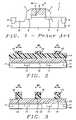
- a conventional MOSFET 1is pictured in FIG. 1 and is typically fabricated by first forming isolation regions 3 such as shallow trench isolation (STI) regions comprised of an insulating material in a substrate 2 .
- isolation regions 3such as shallow trench isolation (STI) regions comprised of an insulating material in a substrate 2 .
- a gate dielectric layer 4is formed on the substrate 2 and a gate layer which may be doped or undoped polysilicon is deposited on the gate dielectric layer 4 .
- the gate layer patternis etch transferred through the gate dielectric layer 4 . Ion implantation is used to form shallow source/drain regions 6 and deep source/drain regions 8 . Sidewall spacers 7 are added adjacent to the gate electrode 5 and gate dielectric layer 4 .
- a silicide layer(not shown) may be formed over the gate electrode 5 and deep source/drain regions 8 and contacts (not shown) may be formed to the silicide layer.
- the gate pattern which defines the gate length dis initially formed by patternwise exposing a photoresist layer (not shown) on the gate layer and developing with an aqueous base to selectively remove exposed or unexposed portions of the photoresist layer depending upon the tone of the photoresist.
- a positive tone photoresistundergoes a reaction in exposed regions that renders them soluble in an aqueous base developer solution while unexposed portions of the photoresist film remain insoluble in the developer.
- exposed regionsare typically crosslinked to become insoluble in a developer while the unexposed portions are washed away in the developer.
- a photoresistmay be applied as a single layer or as the top layer of a bilayer system.
- a single layer photoresistis usually coated over an anti-reflective coating (ARC) that helps to control a subsequent imaging process.
- ARCanti-reflective coating
- a patternis formed in a thin photoresist layer and is etch transferred through a thicker underlayer that is used for its planarization and anti-reflective properties.
- a single layer or bilayer photoresistis selected in which the photoresist (imaging) layer is very opaque to the incident exposing radiation such that only a top portion near the surface absorbs energy and undergoes a chemical change.
- Top surface imaging techniquesare frequently combined with a silylation process which forms O—Si bonds selectively in either the exposed or unexposed regions.
- a silicon containing gasmay react with a phenol group in the polymer component of a photoresist layer to yield O—Si bonds.
- a subsequent plasma etch that includes oxygen chemistryremoves portions of the photoresist that are not protected by the O—Si bonds and thereby produces a pattern without the need of a developer solution.
- the lithography process that is used to pattern the photoresist above the gate layergenerally involves exposure tools which use wavelengths that are selected from a range of about 450 nm (near UV) to approximately 13 nm for extreme UV (EUV) exposures.
- Exposure toolswhich use wavelengths that are selected from a range of about 450 nm (near UV) to approximately 13 nm for extreme UV (EUV) exposures.
- High throughput projection electron beam toolsthat have the capability of imaging 50 to 70 nm resist features may be used in manufacturing in the near future.
- the minimum feature size that can be reliably printed in a photoresist layeris not small enough to meet the demand for sub-100 nm gate lengths for most new devices.
- the industryhas resorted to other methods that involve trimming the photoresist pattern such as an isotropic plasma etch process.
- a plasma etching processemploys the use of a photoresist mask to selectively allow an etchant to remove an underlying layer that has been exposed through openings in the mask pattern.
- the etchantIn an anisotropic etch, the etchant only removes the underlying layer uncovered by the photoresist pattern.
- an isotropic etchinvolves removing exposed portions of the underlying layer along with some of the photoresist along the sidewalls of the openings in the pattern.
- the photoresist layeris not distorted during the etch and should retain a majority of its thickness in order to avoid the formation of edge roughness and sidewall striations that may be transferred into the underlying layer.
- the polymers in photoresists developed for 193 nm or 157 nm lithography applications in new technologiesdo not contain aromatic groups which have an inherently high absorbance below about 240 nm. Therefore, the 193 nm and 157 nm photoresists based on acrylate and cyclic olefin based polymers are not as robust during a plasma etch process as their DUV (248 nm) or i-line (365 nm) predecessors which contain aromatic groups for high etch resistance.
- the thickness of the photoresistmust also decrease to maintain a good focus and exposure latitude.
- the height of a photoresist lineshould not be more than about four times its width in order to prevent a phenomenon called line collapse. Therefore, etching sub-100 nm features using a thin 193 nm or 157 nm based photoresist mask of about 3000 Angstroms or less that has minimal etch resistance is problematic for single layer imaging schemes.
- the 193 nm or 157 nm photoresisthave a lower etch resistance than DUV or i-line photoresists, but a thinner etch mask is used than in conventional DUV or i-line applications.
- the amount of trimming or CD reductionis limited to about 10 nm or less for 193 nm or 157 nm photoresist layers which does not satisfy the need for large scale trimming of about 30 nm or more in many technologies.
- One concept that has been practiced to overcome photoresist etching issuesis to etch a pattern in a photoresist layer into an underlying hard mask that has a much better selectivity towards the gate layer than the photoresist. Once the pattern is transferred, the photoresist layer is stripped and the hard mask serves as the template for the etch transfer step to define the gate length in the gate layer.
- this methodalso has drawbacks including a poor profile control of the hard mask and damage to the gate layer and a silicon substrate when a hardmask such as silicon nitride is removed by phosphoric acid, for example.
- a photoresistis patterned and trimmed on an optional cap layer on a dielectric layer.
- the patternis etched into the cap layer and the photoresist is removed.
- a hard maskis deposited on the cap layer and is planarized to leave a portion of the cap layer exposed.
- the exposed cap layer and underlying dielectric layerare selectively removed by an etch to generate openings above a substrate.
- a photoresist layeris patterned and trimmed above a second hard mask layer.
- the patternis anisotropically etched through the second hard mask which may be SiO 2 .
- a wet etch with H 3 PO 4isotropically transfers the pattern through an underlying first hard mask layer that is silicon nitride and laterally shrinks the first hard mask to a width less than that for the second hard mask.
- the patternis etched into a gate layer.
- a multilayer anti-reflective coating (ARC) processis described in U.S. Pat. No. 6,548,423 in which a photoresist layer is patterned and trimmed above a second ARC which is silicon nitride or SiON. The pattern is anisotropically transferred through the second ARC and a first ARC which is CVD deposited carbon. The photoresist layer is stripped and the pattern is etched into an underlying gate layer using the ARCs as a combined hard mask.
- ARCanti-reflective coating
- etching methodis described in U.S. Pat. No. 6,492,068 in which a photoresist layer is patterned over a bottom ARC (BARC).
- BARCbottom ARC
- the patternis anisotropically etched through the BARC by a gas mixture including Ar, O 2 , Cl 2 , and HBr and is then transferred into an underlying gate layer with a Cl 2 , O 2 , and HBr plasma.
- the photoresist layer, BARC, and gate layerare trimmed simultaneously with an O 2 and HBr plasma etch.
- a bilayer trim etch processis found in U.S. Pat. No. 6,541,360 where a photoresist layer is patterned above an organic layer.
- the patternis isotropically etched with a plasma through the bottom organic layer so that the organic layer has sloped sidewalls and a top that is smaller than its bottom.
- the patternis etched into a gate layer to give a gate length that is smaller than the width of the initial photoresist feature.
- a reproducible gate lengthmay be difficult since it depends on trimming a sloped sidewall in the bottom layer with a high degree of control.
- a new method of trimming a photoresist feature and transferring the resulting pattern into an underlying layeris needed that overcomes the limitations presented by a 157 nm or 193 nm single layer process, an isotropic etch, or a hard mask transfer step.
- One objective of the present inventionis to provide good gate profile control during a method to trim a gate layer to afford a gate length that is smaller than can be generated by a lithography method.
- a further objective of the present inventionis to provide a method of trimming a gate layer where the organic masking layer has sufficient thickness to allow large scale trimming and prevents sidewall striations from forming in the trimmed gate layer.
- a still further objective of the present inventionis to provide a method of trimming a gate layer that does not require a hard mask to be removed after the trimming step.
- Yet another objective of the present inventionis to provide a trimming method that is extendable to forming gate lengths below 100 nm.
- a bilayer resistconsisting of a lower non-photoimageable organic layer and a top photoresist layer is coated on the gate layer.
- the lower layeralso referred to as the underlayer serves as an anti-reflective layer and is also thicker than the photoresist layer since the underlayer will function as an etch mask during a subsequent pattern transfer into the gate layer.
- the underlayeris formed by coating and baking a commercially available BARC, i-line photoresist, or DUV photoresist. When an i-line or DUV photoresist is employed as the underlayer, the underlayer is hard baked to destroy the photosensitive component and prevent interaction with the top photoresist layer.
- the top photoresist layerhas a silicon-containing composition and is preferably a positive tone photoresist.
- the top photoresist layeris preferably patternwise exposed with 193 nm or 157 nm radiation to enable the lithography process to print sub-100 nm features.
- the top photoresist layeris imaged with a shorter wavelength than 157 nm such as 13 nm radiation from an EUV source.
- a key feature of the present inventionis that the photoresist pattern is anisotropically transferred through the underlayer with a plasma etch process based on N 2 /H 2 and SO 2 chemistry. It is important to achieve vertical sidewalls on the underlayer with no etch bias and no line collapse.
- a trimming processthat involves a plasma etch with Cl 2 , HBr, and O 2 gases.
- the bilayer resist profileretains vertical sidewalls while the width of the feature is reduced considerably to a size that cannot be achieved by a lithography method.
- the patternis then transferred through the underlying gate layer to produce a gate length that is equivalent to the width of the trimmed feature in the underlayer.
- the photoresist patternis typically consumed during the gate etch and the underlayer may be removed in a following step by oxygen ashing which results in a patterned gate layer or gate electrode in a partially formed MOSFET.
- a bilayer resist comprised of an upper photoresist layer on an underlayeris coated on a gate layer formed on a gate dielectric layer as in the first embodiment except that the photoresist layer does not contain silicon.
- the top photoresist layeris highly absorbing of the exposing wavelength so that a chemical reaction is induced only near the surface of exposed areas.
- the top surface imaging techniquecontinues with a silylation procedure to selectively silylate regions of photoresist layer above portions of gate layer where a gate electrode is to be subsequently formed.
- the exposed regionsare silylated.
- the exposed regionsare rendered inactive and the silylation occurs in unexposed regions of the top surface.
- a plasma etchis performed to selectively remove portions of the photoresist that are not protected by silylated surface regions.
- FIG. 1is a cross-sectional view of a conventional MOSFET.
- FIG. 2is a cross-sectional view showing the patterning of a top layer in a bilayer resist formed on a gate layer according to one embodiment of the present invention.
- FIG. 3is a cross-sectional view of the structure in FIG. 2 after the pattern is anisotropically etch transferred through the bottom layer (underlayer) of the bilayer resist.
- FIG. 4is a cross-sectional view of the structure in FIG. 3 after the pattern is trimmed by a plasma etch process according to the present invention.
- FIG. 5is a cross-sectional view of the structure in FIG. 4 after the top photoresist layer is removed and the pattern is anisotropically etched through the gate layer.
- FIG. 6is a cross-sectional view of the structure in FIG. 5 after the underlayer is removed by an oxygen ashing step according to the present invention.
- FIG. 7is a cross-sectional view of a bilayer resist in which portions of the top photoresist layer are silylated in exposed surface regions according to a second embodiment of the present invention.
- FIG. 8is a cross-sectional view of the bilayer resist in FIG. 7 that has been etched to remove non-silylated surface regions and underlying portions of the top photoresist layer and underlayer to form a pattern having a first width.
- FIG. 9is a cross-sectional view of a bilayer resist in which portions of the top photoresist layer are silylated in unexposed surface regions according to another embodiment of the present invention.
- FIG. 10is a cross-sectional view that shows silylated surface regions formed between exposed surface regions as a result of the silylation in FIG. 9 .
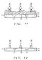
- FIG. 11is a cross-sectional view of the pattern in FIG. 8 that has been trimmed by a plasma etch process of the present invention to form a feature having a second width.
- FIG. 12is a cross-sectional view of the structure in FIG. 11 after the pattern is etched through the gate layer to form a gate electrode and the bottom layer of the bilayer resist is removed according to the present invention
- the present inventionis a method that involves a plasma etch process to reduce the width of a feature in a photoresist pattern in a controlled manner and is particularly useful during the formation of a gate electrode having a gate length that is substantially smaller than can be achieved by a lithography process.
- a plasma etch processto reduce the width of a feature in a photoresist pattern in a controlled manner and is particularly useful during the formation of a gate electrode having a gate length that is substantially smaller than can be achieved by a lithography process.
- a substrate 10is provided which is typically monocrystalline silicon but may be alternatively be based on silicon-germanium, silicon-on-insulator, or other semiconductor materials used in the art. Additionally, substrate 10 may be comprised of active and passive devices that are not shown in order to simplify the drawing. Isolation regions 11 which in the exemplary embodiment are STI regions are formed in the substrate 10 by conventional means and typically contain an insulating layer such as SiO 2 or a low k dielectric material. Between adjacent isolation regions 11 is a p-well or an n-well (not shown) depending on whether a NMOS or a PMOS transistor is to be formed on an overlying active area.
- Isolation regions 11which in the exemplary embodiment are STI regions are formed in the substrate 10 by conventional means and typically contain an insulating layer such as SiO 2 or a low k dielectric material. Between adjacent isolation regions 11 is a p-well or an n-well (not shown) depending on whether a NMOS or a PMOS transistor is to be formed on an over
- a gate stack that includes a gate layer 13 on a gate dielectric layer 12is formed on the substrate 10 .
- a gate dielectric layer 12 with a thickness of about 5 to 100 Angstromsis formed on the substrate 10 by an oxidation method, a chemical vapor deposition (CVD), or by a plasma enhanced CVD (PECVD) technique.
- the gate dielectric layer 12is silicon oxide.
- the gate dielectric layer 12may include a high k dielectric layer comprised of one or more of ZrO 2 , HfO 2 , TiO 2 , Ta 2 O 5 , Al 2 O 3 , Y 2 O 3 , and La 2 O 3 or a silicate, one or more of Zr, Hf, Ti, Ta, Al, Y, and La formed on a thin interfacial layer that is silicon nitride, silicon oxide, or silicon oxynitride.
- High k dielectric layersare formed by a CVD, metal organic CVD (MOCVD), or an atomic layer deposition (ALD) process.
- a gate layer 13 that is doped or undoped polysiliconis deposited by a CVD or PECVD method on the gate dielectric layer 12 and has a thickness between about 500 and 5000 Angstroms.
- the gate layer 13may be comprised of amorphous silicon, SiGe, or SiGeC.
- a bilayer stackcomprised of a top photoresist layer 15 and an organic underlayer hereafter referred to as underlayer 14 is formed on the gate layer 13 .
- An underlayer solutionthat is typically comprised of an organic polymer is commercially available. One source is Arch Chemicals, Inc. of E. Buffalo, R.I. The underlayer solution is spin coated and then baked at a temperature of up to 230° C. to remove organic solvent and form an underlayer 14 that is inactive toward a subsequently coated photoresist layer 15 .
- a commercially available i-line photoresist or Deep UV (DUV) photoresistis spin coated on the gate layer 13 and is baked at a temperature up to about 230° C.
- the resulting underlayer 14has a thickness from about 1000 to 10000 Angstroms and is preferably thicker than the photoresist layer 15 in order to prevent edge roughness and striations in the photoresist pattern from being etch transferred into the gate layer in a later pattern transfer step.
- the underlayer 14typically forms a crosslinked polymer network upon heating and is used to control reflectivity during a subsequent lithographic step in which a pattern is printed in the photoresist layer 15 . Therefore, an underlayer 14 is preferably selected that has a refractive index (n and k values) which minimizes reflectivity of the exposing radiation (not shown) off the underlayer and gate layer 13 into the photoresist layer 15 .
- the photoresist layer 15may have either a positive or a negative tone composition but is preferably a positive tone photoresist that contains silicon and has a thickness between about 100 to 3000 Angstroms.
- a silicon containing photoresist layer 15is employed to provide a high selectivity of the etchant to the thicker underlayer 14 during the etch transfer of the resulting photoresist pattern through the underlayer in a subsequent step. In other words, there should be a minimal thickness loss in the photoresist pattern 15 during a pattern transfer through the underlayer 14 .
- the photoresist layeris patternwise exposed with 193 nm or 157 nm radiation and is developed in an aqueous base solution to generate a photoresist pattern 15 with features (lines) having a width w 1 .
- the photoresist pattern 15is aligned so that a line formed therein is centered approximately midway between the isolation regions 11 .
- a 193 nm or 157 nm exposure wavelengthis necessary to print lines where w 1 is sub-100 nm for advanced technologies.
- a shorter wavelengthsuch as 13 nm radiation from an EUV source or a projection electron beam system may be used to generate a w 1 of less than 100 nm.
- the present inventionalso applies to printing and trimming feature sizes greater than 100 nm.
- the requirement for a controllable etch processis more demanding as w 1 shrinks and the present invention is more beneficial for sub-100 nm applications where prior art methods are limited.
- a key feature of the present inventionis the pattern transfer step through the underlayer 14 .
- a first plasma etch stepis selected for a pattern transfer that maintains vertical sidewalls on the features in the photoresist pattern 15 and forms vertical sidewalls on etched portions of the underlayer 14 .
- the etched underlayer 14has sidewalls with a retrograde profile in which the top of the underlayer has a width w 1 and the bottom has a width slightly less than w 1 .
- the etch conditions employedrepresent an anisotropic process in which feature size w 1 is maintained in the photoresist pattern 15 and is reproduced at least in the top portion of the underlayer 14 .
- the substrate 10 with the photoresist pattern 15 on unpatterned underlayer 14is loaded into a process chamber.
- the underlayer 14is etched with the following process conditions: a 10 to 500 standard cubic centimeter per minute (sccm) flow rate of H 2 , a 10 to 500 sccm N 2 flow rate, a 10 to 500 sccm SO 2 flow rate, a chamber temperature of about 0° C. to 100° C., a RF power from about 100 to 1000 Watts, and a chamber pressure between about 3 mTorr and 500 mTorr.
- the underlayer 14is removed at a rate of about 2000 Angstroms/minute. Etch rate selectivity of the underlayer 14 to the photoresist pattern 15 is about 5:1.
- another critical step in the method of the first embodimentis a trimming process in which the feature size w 1 in the photoresist pattern 15 and underlayer 14 is reduced to w 2 where (w 1 ⁇ w 2 ) may be 10 nm or more. It is important to maintain vertical sidewalls on the underlayer 14 with minimal roughness so that sidewall striations are not produced in the gate layer 13 in a subsequent pattern transfer step.
- a second plasma etch stepthat includes HBr, O 2 , and Cl 2 is performed for the trimming process.
- the second plasma stepis performed in the same process chamber as the first plasma etch step.
- the second plasma etchis performed in a different process chamber within the same mainframe (process tool) used for the first plasma etch.
- the second plasma etch for trimming the feature size from w 1 to w 2 in the photoresist pattern 15 and underlayer 14comprises the following conditions: a 10 to 500 sccm Cl 2 flow rate, a 1 to 50 sccm O 2 flow rate, a 10 to 500 sccm HBr flow rate, a chamber temperature of about 0° C. to 100° C., a RF power from about 100 to 1000 Watts, and a chamber pressure between about 3 and 500 mTorr for a period of about 5 to 200 seconds. Under these conditions, the trimming rate to reduce w 1 to w 2 is about 30 Angstroms per minute.
- the pattern with features having a width w 2 in the underlayer 14is now transferred through the gate layer 13 .
- the photoresist pattern 15may be removed during the second plasma etch step.
- the photoresist pattern 15is removed during a third plasma etch step which follows.
- a third plasma etch step involving an anisotropic etch processis preferred so that vertical sidewalls are formed in the etched gate layer 13 hereafter referred to as gate electrode 13 and in order to form a gate length w 2 with excellent process control.
- an exemplary process for generating a gate length w 2is a Cl 2 flow rate of from 10 to 500 sccm, a HBr flow rate of 10 to 500 sccm, an O 2 flow rate of about 1 to 10 sccm, a chamber temperature from about 0° C. to 100° C., a RF power of about 100 to 1000 Watts, and a chamber pressure from about 3 to 500 mTorr.
- the photoresist pattern 15is typically consumed.
- a small top portion of the underlayer 14may be consumed but a sufficient thickness of the underlayer 14 remains to serve as a stable etch mask during the third plasma etch through the gate layer 13 .
- the third plasma etchis preferably done in the same process chamber as the second plasma etch step.
- the third plasma etch and second plasma etchesare performed in different process chambers within the same process tool.
- the underlayer 14is removed by an oxygen ashing step known to those skilled in the art.
- a gate electrode 13 with a gate length w 2 of less than 100 nmis generated with excellent process control.
- This processis an advantage over a single layer photoresist mask which easily erodes during pattern transfer and yields poor quality profiles with a small process latitude.
- a larger trim (w 1 ⁇ w 2 )is possible with the present invention than in prior art because of improved profile control, especially for sub-100 nm gate lengths.
- the method of the first embodimentoffers better profile control than gate fabrication schemes that involve a hard mask.
- the present inventiondoes not rely on a hard mask, damage to the gate electrode or gate dielectric layer associated with a hard mask removal step is avoided.
- the thick underlayer that serves as a mask during the pattern transfer into the gate layeris an advantage over thinner etch masks since edge roughness in the photoresist layer is prevented from being transferred into the gate layer.
- FIGS. 7-8A second embodiment is illustrated in FIGS. 7-8 .
- a partially formed transistorthat includes a substrate 10 with isolation regions 11 , a gate dielectric layer 12 , a gate layer 13 , and an underlayer 14 is formed as described previously.
- a top photoresist layer 20is coated to a thickness of about 500 to 5000 Angstroms.
- the photoresist layer 20 and underlayer 14form a bilayer stack.
- the photoresist layer 20is preferably a positive tone non-silicon containing photoresist which highly absorbs 157 nm or 193 nm radiation so that during a typical patternwise exposure, only a small portion of the photoresist layer near the surface of an exposed region undergoes a photoinduced reaction.
- a post-exposure bakemay be necessary to increase the rate of the photoinduced reaction in order to decrease process time.
- a shorter wavelength than 157 nmmay be used such as a 13 nm wavelength from an EUV source to patternwise expose the photoresist layer 20 .
- a wavelength of less than 200 nmis preferred to enable the photoresist layer 20 to be selectively exposed in surface regions 21 having a width w 1 of below 100 nm.
- a longer exposure wavelength than 200 nmmay be used if a width w 1 of about 130 nm or larger is desired.
- the photoresist layer 20should not have any polar functionality such as alcohol groups that can be silylated.
- a gas phase treatment 30is preferably employed to silylate the regions 21 .
- the regions 21are comprised of hydroxyl groups which react with a silicon-containing reagent during the gas treatment 30 to form O—Si bonds.
- the gas treatment 30is performed in which a silylating reagent reacts with polar functionalities other than hydroxyl groups to incorporate silicon in regions 21 .
- an organometallic reagentmay be used in place of a silicon containing reagent to react with the regions 21 in the gas treatment 30 to forms regions 21 a which have a high resistance to an etch chemistry based on N 2 /H 2 and SO 2 .
- the resulting silylated regions 21 ahave a higher resistance to an oxygen based etch chemistry than the photoresist layer 20 and underlayer 14 . Therefore, following exposure and the gas treatment 30 , a pattern comprised of lines 23 , 24 , 25 may be developed by a first plasma etch step that includes an oxygen containing gas.
- the first plasma etch step involving N 2 /H 2 and SO 2 described in the first embodimentmay be performed here to form lines 23 , 24 , 25 comprised of a silylated region 21 a having a width w 1 and an underlying portion of the photoresist layer 20 and underlayer 14 .
- a pattern comprised of the lines 23 , 24 , 25is formed by performing a first etch step with an oxygen based etch process such as one including O 2 and Ar, for example.
- Lines 23 , 24 , 25 with a feature size w 1are generated which include a silylated region 21 a and an underlying portion of the photoresist layer 20 .
- the photoresist layer 20 that is not protected by an overlying silylated region 21 ais removed during the etch process. This development process stops on the underlayer 14 .
- a second plasma etch stepinvolving a 10 to 500 sccm flow rate of H 2 , a 10 to 500 sccm N 2 flow rate, a 10 to 500 sccm SO 2 flow rate, a chamber temperature of about 0° C. to 100° C., a RF power from about 100 to 1000 Watts, and a chamber pressure between about 3 mTorr and 500 mTorr may be used to transfer the pattern through the underlayer 14 .
- the etch process through the photoresist layer 20 and underlayer 14results in lines 23 , 24 , 25 that have straight sidewalls and a width w 1 which is a key step of this embodiment.
- the underlayer 14has sidewalls with a retrograde profile in which the top of the underlayer has a width w 1 and the bottom has a width slightly less than w 1 .
- the first and second plasma etch stepsmay be performed in the same process chamber. It is understood that the resulting pattern may include other features (not shown) besides the lines 23 , 24 , 25 as appreciated by those skilled in the art.
- an alternative embodiment for forming a silylated region 21 ainvolves a photoresist layer 20 that is highly absorbing of 157 nm or 193 nm wavelengths and has a polar functionality that can react with a silylation agent or organometallic reagent to form etch resistant regions.
- the photoresist 20is exposed by 157 nm or 193 nm radiation in surface regions 22 to induce a chemical reaction that renders the exposed surface regions inert toward a silylation or organometallic reagent.
- the width between the adjacent surface regions 22is w 1 .
- a gas treatment 30as described previously is carried out to selectively silylate the photoresist layer 20 between the surface regions 22 .
- an organometallic reagentmay be used in place of a silylating reagent in the gas treatment 30 .
- the thickness of the resulting silylated regions 21 ais preferably less than the thickness of the surface regions 22 in order to prevent diffusion of the silylation reagent into the photoresist layer 20 below the surface regions 22 .
- a silylated region 21 ais preferably aligned over the center of an underlying active area between isolation regions 11 .
- pattern comprised of the lines 23 , 24 , 25 having a width w 1 and comprised of a silylated region 21 a and underlying portions of photoresist layer 20 and underlayer 14is formed by either a first plasma etch step comprised of N 2 /H 2 /SO 2 as described previously or a first plasma etch step with an oxygen based plasma to etch through the surface regions 22 and underlying photoresist layer 20 and then a second plasma etch step with N 2 /H 2 /SO 2 to etch through exposed underlayer 14 .
- FIG. 11another critical step in the method of the second embodiment is now executed and is a trimming process in which the feature size w 1 is reduced to w 2 where (w 1 ⁇ w 2 ) may be 10 nm or more. It is important to maintain vertical sidewalls on the underlayer 14 with minimal roughness so that sidewall striations are not produced in the gate layer 13 in a subsequent pattern transfer step.
- a plasma etch stepthat is based on HBr, O 2 , and Cl 2 chemistry as described in the first embodiment is performed for the trimming process. In one embodiment, the plasma etch with HBr, O 2 and Cl 2 is performed in the same process chamber as the H 2 /N 2 /SO 2 plasma etch step.
- the HBr/O 2 /Cl 2 plasma etch and the H 2 /N 2 /SO 2 plasma etchare performed in two different process chambers within the same mainframe (process tool).
- the silylated regions 21 and underlying photoresist layer 20may be removed during the trimming process.
- the silylated regions 21 a and the photoresist layer 20are removed during a gate layer etch step which follows.
- the underlayer 14is used as an etch mask in the next plasma etch step to transfer the lines 23 , 24 , 25 having a width w 2 through the gate layer 13 .
- An anisotropic etch processis preferred so that vertical sidewalls are formed in the etched gate layer (gate electrode) 13 and in order to form a gate length w 2 with excellent process control.
- an exemplary process for generating a gate length w 2is a Cl 2 flow rate of from 10 to 500 sccm, a HBr flow rate of 10 to 500 sccm, an O 2 flow rate of about 1 to 10 sccm, a chamber temperature from about 0° C.
- the silylated layer 21 a and underlying photoresist layer 20are typically consumed and are completely removed. A small top portion of the underlayer 14 may be consumed but a sufficient thickness of the underlayer 14 remains to serve as a stable etch mask during the plasma etch through the gate layer 13 .
- the underlayer 14is removed by an oxygen ashing step to afford a partially formed transistor with a gate electrode 13 .
- a gate electrode 13 having a gate length w 2 of less than 100 nmis generated with excellent process control.
- the benefits of the second embodimentare the same as described previously for the first embodiment and encompass improved profile control on the etch mask and resulting gate electrode, a larger trim amount (w 1 ⁇ w 2 ) than achieved previously, and the avoidance of damage to the gate layer and gate dielectric layer by omitting a hard mask.
- the thick underlayer that serves as a mask during the pattern transfer into the gate layeris an advantage over thinner etch masks since edge roughness in the photoresist layer is prevented from being transferred into the gate electrode.
Landscapes
- Engineering & Computer Science (AREA)
- Physics & Mathematics (AREA)
- Microelectronics & Electronic Packaging (AREA)
- General Physics & Mathematics (AREA)
- Manufacturing & Machinery (AREA)
- Computer Hardware Design (AREA)
- Condensed Matter Physics & Semiconductors (AREA)
- Power Engineering (AREA)
- Chemical & Material Sciences (AREA)
- Chemical Kinetics & Catalysis (AREA)
- General Chemical & Material Sciences (AREA)
- Plasma & Fusion (AREA)
- Drying Of Semiconductors (AREA)
- Photosensitive Polymer And Photoresist Processing (AREA)
- Insulated Gate Type Field-Effect Transistor (AREA)
Abstract
Description
The invention relates to a method of fabricating an integrated circuit in a microelectronic device. More particularly, the present invention is directed to a method of trimming an organic layer in order to reduce a critical dimension below a feature size that can be achieved by lithographic methods.
One of the key steps in the manufacture of a Metal-Oxide-Semiconductor Field Effect Transistor (MOSFET) is formation of a gate electrode comprised of a conducing layer in which a gate length is typically one of the smallest dimensions in the device. To satisfy a constant demand for higher performance devices, the gate length is continually being reduced in each successive technology generation. For current technology, a gate length (LG) as small as 60 or 70 nm is required and LGwill continue to shrink as sub-100 nm technology nodes are implemented in manufacturing. One shortcoming of state of the art lithography processes is that they are incapable of controllably printing features such as a gate in a photoresist layer with a LGsmaller than about 100 nm. To overcome this limitation, many semiconductor fabs use a trimming process which laterally shrinks a photoresist feature such as a line with a plasma etch step.
Aconventional MOSFET 1 is pictured inFIG. 1 and is typically fabricated by first formingisolation regions 3 such as shallow trench isolation (STI) regions comprised of an insulating material in asubstrate 2. A gatedielectric layer 4 is formed on thesubstrate 2 and a gate layer which may be doped or undoped polysilicon is deposited on the gatedielectric layer 4. After the gate layer is patterned by conventional means to form agate electrode 5 having a gate length d, the gate layer pattern is etch transferred through the gatedielectric layer 4. Ion implantation is used to form shallow source/drain regions 6 and deep source/drain regions 8.Sidewall spacers 7 are added adjacent to thegate electrode 5 and gatedielectric layer 4. Subsequently, a silicide layer (not shown) may be formed over thegate electrode 5 and deep source/drain regions 8 and contacts (not shown) may be formed to the silicide layer.
The gate pattern which defines the gate length d is initially formed by patternwise exposing a photoresist layer (not shown) on the gate layer and developing with an aqueous base to selectively remove exposed or unexposed portions of the photoresist layer depending upon the tone of the photoresist. A positive tone photoresist undergoes a reaction in exposed regions that renders them soluble in an aqueous base developer solution while unexposed portions of the photoresist film remain insoluble in the developer. In a negative tone photoresist, exposed regions are typically crosslinked to become insoluble in a developer while the unexposed portions are washed away in the developer.
A photoresist may be applied as a single layer or as the top layer of a bilayer system. A single layer photoresist is usually coated over an anti-reflective coating (ARC) that helps to control a subsequent imaging process. In bilayer applications, a pattern is formed in a thin photoresist layer and is etch transferred through a thicker underlayer that is used for its planarization and anti-reflective properties.
In some cases, a single layer or bilayer photoresist is selected in which the photoresist (imaging) layer is very opaque to the incident exposing radiation such that only a top portion near the surface absorbs energy and undergoes a chemical change. Top surface imaging techniques are frequently combined with a silylation process which forms O—Si bonds selectively in either the exposed or unexposed regions. For example, a silicon containing gas may react with a phenol group in the polymer component of a photoresist layer to yield O—Si bonds. A subsequent plasma etch that includes oxygen chemistry removes portions of the photoresist that are not protected by the O—Si bonds and thereby produces a pattern without the need of a developer solution.
The lithography process that is used to pattern the photoresist above the gate layer generally involves exposure tools which use wavelengths that are selected from a range of about 450 nm (near UV) to approximately 13 nm for extreme UV (EUV) exposures. High throughput projection electron beam tools that have the capability of imaging 50 to 70 nm resist features may be used in manufacturing in the near future. Even with the most advanced exposures tools, phase shifted masks, and other resolution enhancement techniques, the minimum feature size that can be reliably printed in a photoresist layer is not small enough to meet the demand for sub-100 nm gate lengths for most new devices. As a result, the industry has resorted to other methods that involve trimming the photoresist pattern such as an isotropic plasma etch process.
A plasma etching process employs the use of a photoresist mask to selectively allow an etchant to remove an underlying layer that has been exposed through openings in the mask pattern. In an anisotropic etch, the etchant only removes the underlying layer uncovered by the photoresist pattern. On the other hand, an isotropic etch involves removing exposed portions of the underlying layer along with some of the photoresist along the sidewalls of the openings in the pattern. Ideally, the photoresist layer is not distorted during the etch and should retain a majority of its thickness in order to avoid the formation of edge roughness and sidewall striations that may be transferred into the underlying layer. However, the polymers in photoresists developed for 193 nm or 157 nm lithography applications in new technologies do not contain aromatic groups which have an inherently high absorbance below about 240 nm. Therefore, the 193 nm and 157 nm photoresists based on acrylate and cyclic olefin based polymers are not as robust during a plasma etch process as their DUV (248 nm) or i-line (365 nm) predecessors which contain aromatic groups for high etch resistance.
Additionally, as the exposure wavelength shrinks to print smaller features in a photoresist layer, the thickness of the photoresist must also decrease to maintain a good focus and exposure latitude. Generally, the height of a photoresist line should not be more than about four times its width in order to prevent a phenomenon called line collapse. Therefore, etching sub-100 nm features using a thin 193 nm or 157 nm based photoresist mask of about 3000 Angstroms or less that has minimal etch resistance is problematic for single layer imaging schemes. Not only does the 193 nm or 157 nm photoresist have a lower etch resistance than DUV or i-line photoresists, but a thinner etch mask is used than in conventional DUV or i-line applications. At best, the amount of trimming or CD reduction is limited to about 10 nm or less for 193 nm or 157 nm photoresist layers which does not satisfy the need for large scale trimming of about 30 nm or more in many technologies.
One concept that has been practiced to overcome photoresist etching issues is to etch a pattern in a photoresist layer into an underlying hard mask that has a much better selectivity towards the gate layer than the photoresist. Once the pattern is transferred, the photoresist layer is stripped and the hard mask serves as the template for the etch transfer step to define the gate length in the gate layer. However, this method also has drawbacks including a poor profile control of the hard mask and damage to the gate layer and a silicon substrate when a hardmask such as silicon nitride is removed by phosphoric acid, for example.
In U.S. Pat. No. 6,500,755, a photoresist is patterned and trimmed on an optional cap layer on a dielectric layer. The pattern is etched into the cap layer and the photoresist is removed. A hard mask is deposited on the cap layer and is planarized to leave a portion of the cap layer exposed. The exposed cap layer and underlying dielectric layer are selectively removed by an etch to generate openings above a substrate.
In U.S. Pat. No. 6,482,726, a photoresist layer is patterned and trimmed above a second hard mask layer. The pattern is anisotropically etched through the second hard mask which may be SiO2. Once the photoresist layer is removed, a wet etch with H3PO4isotropically transfers the pattern through an underlying first hard mask layer that is silicon nitride and laterally shrinks the first hard mask to a width less than that for the second hard mask. After the second hard mask is removed, the pattern is etched into a gate layer.
A multilayer anti-reflective coating (ARC) process is described in U.S. Pat. No. 6,548,423 in which a photoresist layer is patterned and trimmed above a second ARC which is silicon nitride or SiON. The pattern is anisotropically transferred through the second ARC and a first ARC which is CVD deposited carbon. The photoresist layer is stripped and the pattern is etched into an underlying gate layer using the ARCs as a combined hard mask.
An etching method is described in U.S. Pat. No. 6,492,068 in which a photoresist layer is patterned over a bottom ARC (BARC). The pattern is anisotropically etched through the BARC by a gas mixture including Ar, O2, Cl2, and HBr and is then transferred into an underlying gate layer with a Cl2, O2, and HBr plasma. The photoresist layer, BARC, and gate layer are trimmed simultaneously with an O2and HBr plasma etch.
A bilayer trim etch process is found in U.S. Pat. No. 6,541,360 where a photoresist layer is patterned above an organic layer. The pattern is isotropically etched with a plasma through the bottom organic layer so that the organic layer has sloped sidewalls and a top that is smaller than its bottom. After the top layer is removed, the pattern is etched into a gate layer to give a gate length that is smaller than the width of the initial photoresist feature. However, a reproducible gate length may be difficult since it depends on trimming a sloped sidewall in the bottom layer with a high degree of control.
In U.S. Patent Application Publication US2002/0164543A1, a bilayer photolithography process is described in which an imaging layer is patterned over an underlayer and the pattern is transferred through the underlayer with an O2/HBr plasma process. The method prevents residue from forming on the sidewalls of the etched pattern that normally occurs with an O2/SO2based plasma.
Thus, a new method of trimming a photoresist feature and transferring the resulting pattern into an underlying layer is needed that overcomes the limitations presented by a 157 nm or 193 nm single layer process, an isotropic etch, or a hard mask transfer step.
One objective of the present invention is to provide good gate profile control during a method to trim a gate layer to afford a gate length that is smaller than can be generated by a lithography method.
A further objective of the present invention is to provide a method of trimming a gate layer where the organic masking layer has sufficient thickness to allow large scale trimming and prevents sidewall striations from forming in the trimmed gate layer.
A still further objective of the present invention is to provide a method of trimming a gate layer that does not require a hard mask to be removed after the trimming step.
Yet another objective of the present invention is to provide a trimming method that is extendable to forming gate lengths below 100 nm.
These objectives are achieved by providing a substrate on which a gate dielectric layer and gate layer have been sequentially formed. A bilayer resist consisting of a lower non-photoimageable organic layer and a top photoresist layer is coated on the gate layer. The lower layer also referred to as the underlayer serves as an anti-reflective layer and is also thicker than the photoresist layer since the underlayer will function as an etch mask during a subsequent pattern transfer into the gate layer. The underlayer is formed by coating and baking a commercially available BARC, i-line photoresist, or DUV photoresist. When an i-line or DUV photoresist is employed as the underlayer, the underlayer is hard baked to destroy the photosensitive component and prevent interaction with the top photoresist layer. The top photoresist layer has a silicon-containing composition and is preferably a positive tone photoresist. The top photoresist layer is preferably patternwise exposed with 193 nm or 157 nm radiation to enable the lithography process to print sub-100 nm features. Optionally, the top photoresist layer is imaged with a shorter wavelength than 157 nm such as 13 nm radiation from an EUV source.
A key feature of the present invention is that the photoresist pattern is anisotropically transferred through the underlayer with a plasma etch process based on N2/H2and SO2chemistry. It is important to achieve vertical sidewalls on the underlayer with no etch bias and no line collapse. Next, another crucial step is a trimming process that involves a plasma etch with Cl2, HBr, and O2gases. The bilayer resist profile retains vertical sidewalls while the width of the feature is reduced considerably to a size that cannot be achieved by a lithography method. The pattern is then transferred through the underlying gate layer to produce a gate length that is equivalent to the width of the trimmed feature in the underlayer. The photoresist pattern is typically consumed during the gate etch and the underlayer may be removed in a following step by oxygen ashing which results in a patterned gate layer or gate electrode in a partially formed MOSFET.
In a second embodiment, a bilayer resist comprised of an upper photoresist layer on an underlayer is coated on a gate layer formed on a gate dielectric layer as in the first embodiment except that the photoresist layer does not contain silicon. The top photoresist layer is highly absorbing of the exposing wavelength so that a chemical reaction is induced only near the surface of exposed areas. The top surface imaging technique continues with a silylation procedure to selectively silylate regions of photoresist layer above portions of gate layer where a gate electrode is to be subsequently formed. In one embodiment, the exposed regions are silylated. Alternatively, the exposed regions are rendered inactive and the silylation occurs in unexposed regions of the top surface. Instead of a wet development to form a photoresist pattern as in the first embodiment, a plasma etch is performed to selectively remove portions of the photoresist that are not protected by silylated surface regions.
The remaining steps in the second embodiment including the anisotropic pattern transfer through the underlayer with N2/H2and SO2chemistry and the trim etch with HBr, Cl2and O2gases are the same as described previously in the first embodiment.
The present invention is a method that involves a plasma etch process to reduce the width of a feature in a photoresist pattern in a controlled manner and is particularly useful during the formation of a gate electrode having a gate length that is substantially smaller than can be achieved by a lithography process. Those skilled in the art will appreciate that the invention is not limited to the specific examples described herein and may be applied to trimming photoresist features in other applications. Furthermore, the relative sizes of the various elements shown in the drawings may be different than those in an actual device.
The first embodiment is depicted inFIGS. 2-6 . Referring toFIG. 2 , asubstrate 10 is provided which is typically monocrystalline silicon but may be alternatively be based on silicon-germanium, silicon-on-insulator, or other semiconductor materials used in the art. Additionally,substrate 10 may be comprised of active and passive devices that are not shown in order to simplify the drawing.Isolation regions 11 which in the exemplary embodiment are STI regions are formed in thesubstrate 10 by conventional means and typically contain an insulating layer such as SiO2or a low k dielectric material. Betweenadjacent isolation regions 11 is a p-well or an n-well (not shown) depending on whether a NMOS or a PMOS transistor is to be formed on an overlying active area.
A gate stack that includes agate layer 13 on agate dielectric layer 12 is formed on thesubstrate 10. First, agate dielectric layer 12 with a thickness of about 5 to 100 Angstroms is formed on thesubstrate 10 by an oxidation method, a chemical vapor deposition (CVD), or by a plasma enhanced CVD (PECVD) technique. In one embodiment, thegate dielectric layer 12 is silicon oxide. Alternatively, thegate dielectric layer 12 may include a high k dielectric layer comprised of one or more of ZrO2, HfO2, TiO2, Ta2O5, Al2O3, Y2O3, and La2O3or a silicate, one or more of Zr, Hf, Ti, Ta, Al, Y, and La formed on a thin interfacial layer that is silicon nitride, silicon oxide, or silicon oxynitride. High k dielectric layers are formed by a CVD, metal organic CVD (MOCVD), or an atomic layer deposition (ALD) process.
In one embodiment, agate layer 13 that is doped or undoped polysilicon is deposited by a CVD or PECVD method on thegate dielectric layer 12 and has a thickness between about 500 and 5000 Angstroms. Optionally, thegate layer 13 may be comprised of amorphous silicon, SiGe, or SiGeC.
Next, a bilayer stack comprised of atop photoresist layer 15 and an organic underlayer hereafter referred to asunderlayer 14 is formed on thegate layer 13. An underlayer solution that is typically comprised of an organic polymer is commercially available. One source is Arch Chemicals, Inc. of E. Providence, R.I. The underlayer solution is spin coated and then baked at a temperature of up to 230° C. to remove organic solvent and form anunderlayer 14 that is inactive toward a subsequentlycoated photoresist layer 15. Optionally, a commercially available i-line photoresist or Deep UV (DUV) photoresist is spin coated on thegate layer 13 and is baked at a temperature up to about 230° C. to remove organic solvents and to render the photosensitive components inactive. The resultingunderlayer 14 has a thickness from about 1000 to 10000 Angstroms and is preferably thicker than thephotoresist layer 15 in order to prevent edge roughness and striations in the photoresist pattern from being etch transferred into the gate layer in a later pattern transfer step. Theunderlayer 14 typically forms a crosslinked polymer network upon heating and is used to control reflectivity during a subsequent lithographic step in which a pattern is printed in thephotoresist layer 15. Therefore, anunderlayer 14 is preferably selected that has a refractive index (n and k values) which minimizes reflectivity of the exposing radiation (not shown) off the underlayer andgate layer 13 into thephotoresist layer 15.
Thephotoresist layer 15 may have either a positive or a negative tone composition but is preferably a positive tone photoresist that contains silicon and has a thickness between about 100 to 3000 Angstroms. A silicon containingphotoresist layer 15 is employed to provide a high selectivity of the etchant to thethicker underlayer 14 during the etch transfer of the resulting photoresist pattern through the underlayer in a subsequent step. In other words, there should be a minimal thickness loss in thephotoresist pattern 15 during a pattern transfer through theunderlayer 14. Preferably, the photoresist layer is patternwise exposed with 193 nm or 157 nm radiation and is developed in an aqueous base solution to generate aphotoresist pattern 15 with features (lines) having a width w1. Note that thephotoresist pattern 15 is aligned so that a line formed therein is centered approximately midway between theisolation regions 11. A 193 nm or 157 nm exposure wavelength is necessary to print lines where w1is sub-100 nm for advanced technologies. Optionally, a shorter wavelength such as 13 nm radiation from an EUV source or a projection electron beam system may be used to generate a w1of less than 100 nm. It should be understood that the present invention also applies to printing and trimming feature sizes greater than 100 nm. However, the requirement for a controllable etch process is more demanding as w1shrinks and the present invention is more beneficial for sub-100 nm applications where prior art methods are limited.
Referring toFIG. 3 , a key feature of the present invention is the pattern transfer step through theunderlayer 14. A first plasma etch step is selected for a pattern transfer that maintains vertical sidewalls on the features in thephotoresist pattern 15 and forms vertical sidewalls on etched portions of theunderlayer 14. Alternatively, the etchedunderlayer 14 has sidewalls with a retrograde profile in which the top of the underlayer has a width w1and the bottom has a width slightly less than w1. The etch conditions employed represent an anisotropic process in which feature size w1is maintained in thephotoresist pattern 15 and is reproduced at least in the top portion of theunderlayer 14. The inventors have discovered that an etch chemistry based on H2, N2, and SO2provides the required results. In a preferred embodiment, thesubstrate 10 with thephotoresist pattern 15 onunpatterned underlayer 14 is loaded into a process chamber. Theunderlayer 14 is etched with the following process conditions: a 10 to 500 standard cubic centimeter per minute (sccm) flow rate of H2, a 10 to 500 sccm N2flow rate, a 10 to 500 sccm SO2flow rate, a chamber temperature of about 0° C. to 100° C., a RF power from about 100 to 1000 Watts, and a chamber pressure between about 3 mTorr and 500 mTorr. Theunderlayer 14 is removed at a rate of about 2000 Angstroms/minute. Etch rate selectivity of theunderlayer 14 to thephotoresist pattern 15 is about 5:1.
Referring toFIG. 4 , another critical step in the method of the first embodiment is a trimming process in which the feature size w1in thephotoresist pattern 15 andunderlayer 14 is reduced to w2where (w1−w2) may be 10 nm or more. It is important to maintain vertical sidewalls on theunderlayer 14 with minimal roughness so that sidewall striations are not produced in thegate layer 13 in a subsequent pattern transfer step. A second plasma etch step that includes HBr, O2, and Cl2is performed for the trimming process. In one embodiment, the second plasma step is performed in the same process chamber as the first plasma etch step. Optionally, the second plasma etch is performed in a different process chamber within the same mainframe (process tool) used for the first plasma etch.
The second plasma etch for trimming the feature size from w1to w2in thephotoresist pattern 15 andunderlayer 14 comprises the following conditions: a 10 to 500 sccm Cl2flow rate, a 1 to 50 sccm O2flow rate, a 10 to 500 sccm HBr flow rate, a chamber temperature of about 0° C. to 100° C., a RF power from about 100 to 1000 Watts, and a chamber pressure between about 3 and 500 mTorr for a period of about 5 to 200 seconds. Under these conditions, the trimming rate to reduce w1to w2is about 30 Angstroms per minute.
Referring toFIG. 5 , the pattern with features having a width w2in theunderlayer 14 is now transferred through thegate layer 13. Note that thephotoresist pattern 15 may be removed during the second plasma etch step. Optionally, thephotoresist pattern 15 is removed during a third plasma etch step which follows. A third plasma etch step involving an anisotropic etch process is preferred so that vertical sidewalls are formed in the etchedgate layer 13 hereafter referred to asgate electrode 13 and in order to form a gate length w2with excellent process control. When thegate layer 13 is polysilicon, an exemplary process for generating a gate length w2is a Cl2flow rate of from 10 to 500 sccm, a HBr flow rate of 10 to 500 sccm, an O2flow rate of about 1 to 10 sccm, a chamber temperature from about 0° C. to 100° C., a RF power of about 100 to 1000 Watts, and a chamber pressure from about 3 to 500 mTorr. Under these conditions, thephotoresist pattern 15 is typically consumed. A small top portion of theunderlayer 14 may be consumed but a sufficient thickness of theunderlayer 14 remains to serve as a stable etch mask during the third plasma etch through thegate layer 13. The third plasma etch is preferably done in the same process chamber as the second plasma etch step. Optionally, the third plasma etch and second plasma etches are performed in different process chambers within the same process tool.
Referring toFIG. 6 , theunderlayer 14 is removed by an oxygen ashing step known to those skilled in the art. As a result, agate electrode 13 with a gate length w2of less than 100 nm is generated with excellent process control. This process is an advantage over a single layer photoresist mask which easily erodes during pattern transfer and yields poor quality profiles with a small process latitude. A larger trim (w1−w2) is possible with the present invention than in prior art because of improved profile control, especially for sub-100 nm gate lengths. Likewise, the method of the first embodiment offers better profile control than gate fabrication schemes that involve a hard mask. Since the present invention does not rely on a hard mask, damage to the gate electrode or gate dielectric layer associated with a hard mask removal step is avoided. The thick underlayer that serves as a mask during the pattern transfer into the gate layer is an advantage over thinner etch masks since edge roughness in the photoresist layer is prevented from being transferred into the gate layer.
A second embodiment is illustrated inFIGS. 7-8 . Referring toFIG. 7 , a partially formed transistor that includes asubstrate 10 withisolation regions 11, agate dielectric layer 12, agate layer 13, and anunderlayer 14 is formed as described previously. Atop photoresist layer 20 is coated to a thickness of about 500 to 5000 Angstroms. Thephotoresist layer 20 andunderlayer 14 form a bilayer stack. Thephotoresist layer 20 is preferably a positive tone non-silicon containing photoresist which highly absorbs 157 nm or 193 nm radiation so that during a typical patternwise exposure, only a small portion of the photoresist layer near the surface of an exposed region undergoes a photoinduced reaction. It is understood that a post-exposure bake may be necessary to increase the rate of the photoinduced reaction in order to decrease process time. Alternatively, a shorter wavelength than 157 nm may be used such as a 13 nm wavelength from an EUV source to patternwise expose thephotoresist layer 20. A wavelength of less than 200 nm is preferred to enable thephotoresist layer 20 to be selectively exposed insurface regions 21 having a width w1of below 100 nm. In an alternative embodiment, a longer exposure wavelength than 200 nm may be used if a width w1of about 130 nm or larger is desired.
The exposure chemically alters theregions 21 of thephotoresist layer 20 so that theregions 21 may be selectively silylated by a conventional method known to those skilled in the art. Therefore, thephotoresist layer 20 should not have any polar functionality such as alcohol groups that can be silylated. Both gas phase and liquid phase silylations are practiced in the art but in the exemplary embodiment agas phase treatment 30 is preferably employed to silylate theregions 21. In one embodiment, theregions 21 are comprised of hydroxyl groups which react with a silicon-containing reagent during thegas treatment 30 to form O—Si bonds. Optionally, thegas treatment 30 is performed in which a silylating reagent reacts with polar functionalities other than hydroxyl groups to incorporate silicon inregions 21. In another embodiment, an organometallic reagent may be used in place of a silicon containing reagent to react with theregions 21 in thegas treatment 30 toforms regions 21awhich have a high resistance to an etch chemistry based on N2/H2and SO2.
Referring toFIG. 8 , the resultingsilylated regions 21ahave a higher resistance to an oxygen based etch chemistry than thephotoresist layer 20 andunderlayer 14. Therefore, following exposure and thegas treatment 30, a pattern comprised oflines lines silylated region 21ahaving a width w1and an underlying portion of thephotoresist layer 20 andunderlayer 14.
In another embodiment, a pattern comprised of thelines Lines silylated region 21aand an underlying portion of thephotoresist layer 20. Thephotoresist layer 20 that is not protected by an overlyingsilylated region 21ais removed during the etch process. This development process stops on theunderlayer 14. Next, a second plasma etch step involving a 10 to 500 sccm flow rate of H2, a 10 to 500 sccm N2flow rate, a 10 to 500 sccm SO2flow rate, a chamber temperature of about 0° C. to 100° C., a RF power from about 100 to 1000 Watts, and a chamber pressure between about 3 mTorr and 500 mTorr may be used to transfer the pattern through theunderlayer 14. The etch process through thephotoresist layer 20 andunderlayer 14 results inlines underlayer 14 has sidewalls with a retrograde profile in which the top of the underlayer has a width w1and the bottom has a width slightly less than w1. The first and second plasma etch steps may be performed in the same process chamber. It is understood that the resulting pattern may include other features (not shown) besides thelines
Referring toFIG. 9 , an alternative embodiment for forming asilylated region 21ainvolves aphotoresist layer 20 that is highly absorbing of 157 nm or 193 nm wavelengths and has a polar functionality that can react with a silylation agent or organometallic reagent to form etch resistant regions. Thephotoresist 20 is exposed by 157 nm or 193 nm radiation insurface regions 22 to induce a chemical reaction that renders the exposed surface regions inert toward a silylation or organometallic reagent. The width between theadjacent surface regions 22 is w1. Then agas treatment 30 as described previously is carried out to selectively silylate thephotoresist layer 20 between thesurface regions 22. Alternatively, an organometallic reagent may be used in place of a silylating reagent in thegas treatment 30.
Referring toFIG. 10 , the thickness of the resultingsilylated regions 21ais preferably less than the thickness of thesurface regions 22 in order to prevent diffusion of the silylation reagent into thephotoresist layer 20 below thesurface regions 22. Note that asilylated region 21ais preferably aligned over the center of an underlying active area betweenisolation regions 11.
Referring again toFIG. 8 , pattern comprised of thelines silylated region 21aand underlying portions ofphotoresist layer 20 andunderlayer 14 is formed by either a first plasma etch step comprised of N2/H2/SO2as described previously or a first plasma etch step with an oxygen based plasma to etch through thesurface regions 22 andunderlying photoresist layer 20 and then a second plasma etch step with N2/H2/SO2to etch through exposedunderlayer 14.
Referring toFIG. 11 , another critical step in the method of the second embodiment is now executed and is a trimming process in which the feature size w1is reduced to w2where (w1−w2) may be 10 nm or more. It is important to maintain vertical sidewalls on theunderlayer 14 with minimal roughness so that sidewall striations are not produced in thegate layer 13 in a subsequent pattern transfer step. A plasma etch step that is based on HBr, O2, and Cl2chemistry as described in the first embodiment is performed for the trimming process. In one embodiment, the plasma etch with HBr, O2and Cl2is performed in the same process chamber as the H2/N2/SO2plasma etch step. Optionally, the HBr/O2/Cl2plasma etch and the H2/N2/SO2plasma etch are performed in two different process chambers within the same mainframe (process tool). Note that thesilylated regions 21 andunderlying photoresist layer 20 may be removed during the trimming process. Optionally, thesilylated regions 21aand thephotoresist layer 20 are removed during a gate layer etch step which follows.
Theunderlayer 14 is used as an etch mask in the next plasma etch step to transfer thelines gate layer 13. An anisotropic etch process is preferred so that vertical sidewalls are formed in the etched gate layer (gate electrode)13 and in order to form a gate length w2with excellent process control. When thegate layer 13 is polysilicon, an exemplary process for generating a gate length w2is a Cl2flow rate of from 10 to 500 sccm, a HBr flow rate of 10 to 500 sccm, an O2flow rate of about 1 to 10 sccm, a chamber temperature from about 0° C. to 100° C., a RF power of about 100 to 1000 Watts, and a chamber pressure from about 3 to 500 mTorr. Under these conditions, thesilylated layer 21aandunderlying photoresist layer 20 are typically consumed and are completely removed. A small top portion of theunderlayer 14 may be consumed but a sufficient thickness of theunderlayer 14 remains to serve as a stable etch mask during the plasma etch through thegate layer 13.
Referring toFIG. 12 , theunderlayer 14 is removed by an oxygen ashing step to afford a partially formed transistor with agate electrode 13. As a result, agate electrode 13 having a gate length w2of less than 100 nm is generated with excellent process control. The benefits of the second embodiment are the same as described previously for the first embodiment and encompass improved profile control on the etch mask and resulting gate electrode, a larger trim amount (w1−w2) than achieved previously, and the avoidance of damage to the gate layer and gate dielectric layer by omitting a hard mask. Furthermore, the thick underlayer that serves as a mask during the pattern transfer into the gate layer is an advantage over thinner etch masks since edge roughness in the photoresist layer is prevented from being transferred into the gate electrode.
While this invention has been particularly shown and described with reference to, the preferred embodiments thereof, it will be understood by those skilled in the art that various changes in form and details may be made without departing from the spirit and scope of this invention.
Claims (37)
1. A method of trimming a feature in a pattern formed in a photoresist layer on a substrate, comprising:
providing a substrate;
forming a bilayer stack comprised of a top photoresist layer and an organic underlayer on said substrate, said organic underlayer is thicker than said top photoresist layer;
forming a pattern having a feature with a first width in said top photoresist layer;
transferring said pattern through the organic underlayer with a first plasma etch step to produce a pattern that has a feature with a first width and sidewalls; and
trimming said pattern with a second plasma etch step to give a pattern in the bilayer stack having a feature with a second width and sidewalls, said second width is smaller than said first width.
2. The method ofclaim 1 wherein the top photoresist layer is a silicon containing positive tone photoresist that is patterned by exposing with 193 nm, 157 nm, or EUV radiation and developing in an aqueous base solution.
3. The method ofclaim 1 wherein the organic underlayer has a thickness of about 1000 to 10000 Angstroms and does not react with the top photoresist layer during the photoresist coating and patterning steps.
4. The method ofclaim 1 wherein said first width in said top photoresist layer is less than 100 nm.
5. The method ofclaim 1 wherein the first plasma etch step comprises the following conditions: a 10 to 500 standard cubic centimeter per minute (sccm) flow rate of H2; a 10 to 500 sccm flow rate of N2; a 10 to 500 sccm flow rate of SO2; a chamber temperature of about 0° C. to 100° C.; a RF power from about 100 to 1000 Watts; and a chamber pressure between about 3 and 500 mTorr.
6. The method ofclaim 1 wherein the second plasma etch step comprises the following conditions: a 10 to 500 sccm Cl2 flow rate; a 1 to 50 sccm O2 flow rate; a 10 to 50 sccm HBr flow rate; a chamber temperature of about 0° C. to 100° C.; a RF power from about 100 to 1000 Watts; and a chamber pressure between about 3 and 500 mTorr for a period of about 5 to 200 seconds.
7. The method ofclaim 1 wherein the first and second plasma etch steps are performed in the same process chamber.
8. The method ofclaim 1 wherein the second width is more than about 10 nm smaller than the first width.
9. The method ofclaim 1 further comprised of transferring the pattern into said substrate with a third plasma etch step in the same process chamber as used for the second plasma etch step.
10. The method ofclaim 1 wherein the sidewalls formed on the organic underlayer portion of said feature are vertical or have a retrograde profile.
11. The method ofclaim 1 wherein the substrate includes isolation regions formed therein and a gate stack comprised of a gate layer on a gate dielectric layer formed on said substrate between said isolation regions.
12. The method ofclaim 11 further comprising:
selectively silylating portions of the top photoresist layer to give silylated portions having the first width; and
wherein the step of forming a pattern includes removing non-silylated portions in the surface region and the underlying top photoresist layer.
13. A method of forming a gate electrode in a MOSFET, comprising:
providing a substrate with isolation regions formed therein and with a gate stack comprised of a gate layer on a gate dielectric layer formed on said substrate between said isolation regions;
forming a bilayer stack comprised of a top photoresist layer and an organic underlayer on said gate layer, said organic underlayer is thicker than said top photoresist layer;
forming a pattern having a feature with a first width in said top photoresist layer;
transferring said pattern through the organic underlayer with a first plasma etch step to produce a pattern that has a feature with a first width and sidewalls;
trimming said pattern in said top photoresist and organic underlayer with a second plasma etch step to give a pattern in the bilayer stack having a feature with a second width and sidewalls, said second width is smaller than said first width; and
transferring said trimmed pattern with said second width through said gate layer with a third plasma etch step to form a gate electrode.
14. The method ofclaim 13 wherein the gate layer is polysilicon with a thickness between about 500 and 5000 Angstroms.
15. The method ofclaim 13 wherein the top photoresist is a silicon containing positive tone photoresist that is patterned by exposing with 193 nm, 157 nm, or EUV radiation and developing in an aqueous base solution.
16. The method ofclaim 13 wherein the organic underlayer has a thickness of about 1000 to 10000 Angstroms and does not react with the top photoresist layer during the photoresist coating and patterning steps.
17. The method ofclaim 13 wherein said first width in said top photoresist layer is less than about 100 nm.
18. The method ofclaim 13 wherein the first plasma etch step comprises a 10 to 500 sccm flow rate of H2, a 10 to 500 sccm flow rate of N2, a 10 to 500 sccm flow rate of SO2, a chamber temperature of about 0° C. to 100° C., a RF power from about 100 to 1000 Watts, and a chamber pressure between about 3 and 500 mTorr.
19. The method ofclaim 13 wherein the second plasma etch step comprises a 10 to 500 sccm Cl2 flow rate, a 1 to 50 sccm O2 flow rate, a 10 to 50 sccm HBr flow rate, a chamber temperature of about 0° C. to 100° C., a RF power from about 100 to 1000 Watts, and a chamber pressure between about 3 and 500 mTorr for a period of about 5 to 200 seconds.
20. The method ofclaim 13 wherein the second width is more than about 10 nm smaller than the first width.
21. The method ofclaim 13 wherein the sidewalls formed on the organic underlayer portion of said feature are vertical or have a retrograde profile.
22. The method ofclaim 13 wherein the third plasma etch step comprises a 10 to 500 sccm flow rate of Cl2, a 10 to 500 sccm flow rate of HBr, a 1 to 10 sccm flow rate of O2, a chamber temperature of about 0° C. to 100° C., a RF power from about 100 to 1000 Watts, and a chamber pressure between about 3 and 500 mTorr.
23. The method ofclaim 13 wherein the third plasma etch step is performed in the same process chamber as the second plasma etch step and removes the top photoresist layer.
24. The method ofclaim 23 further comprised of removing the underlayer after the third plasma etch step by an oxygen ashing process.
25. A method of forming a gate electrode in a MOSFET, comprising:
providing a substrate with isolation regions formed therein and with a gate stack comprised of a gate layer on a gate dielectric layer formed on said substrate between said isolation regions;
forming a bilayer stack comprised of a top photoresist layer with a surface region and an organic underlayer on said gate layer, said organic underlayer is thicker than said top photoresist layer;
patternwise exposing a surface region of the top photoresist layer;
selectively silylating portions of the top photoresist layer to give silylated portions having a first width;
forming a pattern having a feature with a first width in said top photoresist layer by a first plasma etch step that removes non-silylated portions in the surface region and the underlying top photoresist layer;
transferring said pattern through the organic underlayer with a second plasma etch step, said pattern has a feature with sidewalls and a first width;
trimming said pattern in said top photoresist layer and organic underlayer with a third plasma etch step to give a pattern in the bilayer stack having a feature with sidewalls and a second width, said second width is smaller than said first width;
transferring said trimmed pattern with said second width through said gatelayer with a fourth plasma etch step to form a gate electrode having a second width.
26. The method ofclaim 25 wherein the gate layer is polysilicon with a thickness between about 500 and 5000 Angstroms.
27. The method ofclaim 25 wherein the top photoresist is patternwise exposed with 193 nm, 157 nm, or EUV (13 nm) wavelengths that chemically alter only the exposed surface region of said top photoresist.
28. The method ofclaim 25 wherein the underlayer has a thickness of about 1000 to 10000 Angstroms and does not react with the photoresist layer during the photoresist coating and patterning steps.
29. The method ofclaim 25 wherein the first plasma etch comprises an oxygen containing plasma.
30. The method ofclaim 25 wherein the second plasma etch step comprises a 10 to 500 sccm flow rate of H2, a 10 to 500 sccm flow rate of N2, a 10 to 500 sccm flow rate of SO2, a chamber temperature of about 0° C. to 100° C., a RF power from about 100 to 1000 Watts, and a chamber pressure between about 3 and 500 mTorr.
31. The method ofclaim 25 wherein the third plasma etch step comprises a 10 to 500 sccm Cl2 flow rate, a 1 to 50 sccm O2 flow rate, a 10 to 50 sccm HBr flow rate, a chamber temperature of about 0° C. to 100° C., a RF power from about 100 to 1000 Watts, and a chamber pressure between about 3 and 500 mTorr for a period of about 5 to 200 seconds.
32. The method ofclaim 25 wherein the second width is more than about 10 nm smaller than the first width.
33. The method ofclaim 25 wherein the fourth plasma etch step is performed in the same chamber as the third plasma etch step and removes the top photoresist layer.
34. The method ofclaim 25 wherein the fourth plasma etch step comprises a 10 to 500 sccm flow rate of Cl2, a 10 to 500 sccm flow rate of HBr, a 1 to 10 sccm flow rate of O2, a chamber temperature of about 0° C. to 100° C., a RF power from about 100 to 1000 Watts, and a chamber pressure between about 3 and 500 mTorr.
35. The method ofclaim 25 further comprised of removing the underlayer after the fourth plasma etch step by an oxygen ashing process.
36. The method ofclaim 25 wherein said exposed surface regions of the top photoresist layer are selectively silylated.
37. The method ofclaim 25 wherein portions of the top photoresist layer between said exposed surface regions are selectively silylated.
Priority Applications (2)
| Application Number | Priority Date | Filing Date | Title |
|---|---|---|---|
| US10/764,913US7354847B2 (en) | 2004-01-26 | 2004-01-26 | Method of trimming technology |
| TW093124469ATWI236051B (en) | 2004-01-26 | 2004-08-13 | A novel method of trimming technology |
Applications Claiming Priority (1)
| Application Number | Priority Date | Filing Date | Title |
|---|---|---|---|
| US10/764,913US7354847B2 (en) | 2004-01-26 | 2004-01-26 | Method of trimming technology |
Publications (2)
| Publication Number | Publication Date |
|---|---|
| US20050164478A1 US20050164478A1 (en) | 2005-07-28 |
| US7354847B2true US7354847B2 (en) | 2008-04-08 |
Family
ID=34795376
Family Applications (1)
| Application Number | Title | Priority Date | Filing Date |
|---|---|---|---|
| US10/764,913Expired - LifetimeUS7354847B2 (en) | 2004-01-26 | 2004-01-26 | Method of trimming technology |
Country Status (2)
| Country | Link |
|---|---|
| US (1) | US7354847B2 (en) |
| TW (1) | TWI236051B (en) |
Cited By (394)
| Publication number | Priority date | Publication date | Assignee | Title |
|---|---|---|---|---|
| US20100105207A1 (en)* | 2008-10-23 | 2010-04-29 | Ki-Jun Yun | Method for forming fine pattern of semiconductor device |
| US20110151655A1 (en)* | 2009-12-18 | 2011-06-23 | Bor-Wen Chan | Metal gate fill and method of making |
| US8334083B2 (en) | 2011-03-22 | 2012-12-18 | Tokyo Electron Limited | Etch process for controlling pattern CD and integrity in multi-layer masks |
| US20140273479A1 (en)* | 2013-03-15 | 2014-09-18 | Wafertech, Llc | Plasma pre-treatment for improved uniformity in semiconductor manufacturing |
| US20150118846A1 (en)* | 2013-10-28 | 2015-04-30 | Asm Ip Holding B.V. | Method For Trimming Carbon-Containing Film At Reduced Trimming Rate |
| US9105587B2 (en) | 2012-11-08 | 2015-08-11 | Micron Technology, Inc. | Methods of forming semiconductor structures with sulfur dioxide etch chemistries |
| US9324811B2 (en) | 2012-09-26 | 2016-04-26 | Asm Ip Holding B.V. | Structures and devices including a tensile-stressed silicon arsenic layer and methods of forming same |
| US9384987B2 (en) | 2012-04-04 | 2016-07-05 | Asm Ip Holding B.V. | Metal oxide protective layer for a semiconductor device |
| US9394608B2 (en) | 2009-04-06 | 2016-07-19 | Asm America, Inc. | Semiconductor processing reactor and components thereof |
| US9404587B2 (en) | 2014-04-24 | 2016-08-02 | ASM IP Holding B.V | Lockout tagout for semiconductor vacuum valve |
| US9412564B2 (en) | 2013-07-22 | 2016-08-09 | Asm Ip Holding B.V. | Semiconductor reaction chamber with plasma capabilities |
| US9447498B2 (en) | 2014-03-18 | 2016-09-20 | Asm Ip Holding B.V. | Method for performing uniform processing in gas system-sharing multiple reaction chambers |
| US9455138B1 (en) | 2015-11-10 | 2016-09-27 | Asm Ip Holding B.V. | Method for forming dielectric film in trenches by PEALD using H-containing gas |
| US9478415B2 (en) | 2015-02-13 | 2016-10-25 | Asm Ip Holding B.V. | Method for forming film having low resistance and shallow junction depth |
| US9484191B2 (en) | 2013-03-08 | 2016-11-01 | Asm Ip Holding B.V. | Pulsed remote plasma method and system |
| US9543180B2 (en) | 2014-08-01 | 2017-01-10 | Asm Ip Holding B.V. | Apparatus and method for transporting wafers between wafer carrier and process tool under vacuum |
| US9556516B2 (en) | 2013-10-09 | 2017-01-31 | ASM IP Holding B.V | Method for forming Ti-containing film by PEALD using TDMAT or TDEAT |
| US9558931B2 (en) | 2012-07-27 | 2017-01-31 | Asm Ip Holding B.V. | System and method for gas-phase sulfur passivation of a semiconductor surface |
| US9589770B2 (en) | 2013-03-08 | 2017-03-07 | Asm Ip Holding B.V. | Method and systems for in-situ formation of intermediate reactive species |
| US9605342B2 (en) | 2012-09-12 | 2017-03-28 | Asm Ip Holding B.V. | Process gas management for an inductively-coupled plasma deposition reactor |
| US9607837B1 (en) | 2015-12-21 | 2017-03-28 | Asm Ip Holding B.V. | Method for forming silicon oxide cap layer for solid state diffusion process |
| US9627221B1 (en) | 2015-12-28 | 2017-04-18 | Asm Ip Holding B.V. | Continuous process incorporating atomic layer etching |
| US9640416B2 (en) | 2012-12-26 | 2017-05-02 | Asm Ip Holding B.V. | Single-and dual-chamber module-attachable wafer-handling chamber |
| US9647114B2 (en) | 2015-08-14 | 2017-05-09 | Asm Ip Holding B.V. | Methods of forming highly p-type doped germanium tin films and structures and devices including the films |
| US9657845B2 (en) | 2014-10-07 | 2017-05-23 | Asm Ip Holding B.V. | Variable conductance gas distribution apparatus and method |
| US9659799B2 (en) | 2012-08-28 | 2017-05-23 | Asm Ip Holding B.V. | Systems and methods for dynamic semiconductor process scheduling |
| US9711345B2 (en) | 2015-08-25 | 2017-07-18 | Asm Ip Holding B.V. | Method for forming aluminum nitride-based film by PEALD |
| US9735024B2 (en) | 2015-12-28 | 2017-08-15 | Asm Ip Holding B.V. | Method of atomic layer etching using functional group-containing fluorocarbon |
| US9754779B1 (en) | 2016-02-19 | 2017-09-05 | Asm Ip Holding B.V. | Method for forming silicon nitride film selectively on sidewalls or flat surfaces of trenches |
| US9793115B2 (en) | 2013-08-14 | 2017-10-17 | Asm Ip Holding B.V. | Structures and devices including germanium-tin films and methods of forming same |
| US9793148B2 (en) | 2011-06-22 | 2017-10-17 | Asm Japan K.K. | Method for positioning wafers in multiple wafer transport |
| US9790595B2 (en) | 2013-07-12 | 2017-10-17 | Asm Ip Holding B.V. | Method and system to reduce outgassing in a reaction chamber |
| US9793135B1 (en) | 2016-07-14 | 2017-10-17 | ASM IP Holding B.V | Method of cyclic dry etching using etchant film |
| US9812320B1 (en) | 2016-07-28 | 2017-11-07 | Asm Ip Holding B.V. | Method and apparatus for filling a gap |
| US9859151B1 (en) | 2016-07-08 | 2018-01-02 | Asm Ip Holding B.V. | Selective film deposition method to form air gaps |
| US9887082B1 (en) | 2016-07-28 | 2018-02-06 | Asm Ip Holding B.V. | Method and apparatus for filling a gap |
| US9891521B2 (en) | 2014-11-19 | 2018-02-13 | Asm Ip Holding B.V. | Method for depositing thin film |
| US9890456B2 (en) | 2014-08-21 | 2018-02-13 | Asm Ip Holding B.V. | Method and system for in situ formation of gas-phase compounds |
| US9892908B2 (en) | 2011-10-28 | 2018-02-13 | Asm America, Inc. | Process feed management for semiconductor substrate processing |
| US9899291B2 (en) | 2015-07-13 | 2018-02-20 | Asm Ip Holding B.V. | Method for protecting layer by forming hydrocarbon-based extremely thin film |
| US9899405B2 (en) | 2014-12-22 | 2018-02-20 | Asm Ip Holding B.V. | Semiconductor device and manufacturing method thereof |
| US9905420B2 (en) | 2015-12-01 | 2018-02-27 | Asm Ip Holding B.V. | Methods of forming silicon germanium tin films and structures and devices including the films |
| US9909214B2 (en) | 2015-10-15 | 2018-03-06 | Asm Ip Holding B.V. | Method for depositing dielectric film in trenches by PEALD |
| US9916980B1 (en) | 2016-12-15 | 2018-03-13 | Asm Ip Holding B.V. | Method of forming a structure on a substrate |
| US9960072B2 (en) | 2015-09-29 | 2018-05-01 | Asm Ip Holding B.V. | Variable adjustment for precise matching of multiple chamber cavity housings |
| US10032628B2 (en) | 2016-05-02 | 2018-07-24 | Asm Ip Holding B.V. | Source/drain performance through conformal solid state doping |
| US10043661B2 (en) | 2015-07-13 | 2018-08-07 | Asm Ip Holding B.V. | Method for protecting layer by forming hydrocarbon-based extremely thin film |
| US10083836B2 (en) | 2015-07-24 | 2018-09-25 | Asm Ip Holding B.V. | Formation of boron-doped titanium metal films with high work function |
| US10087522B2 (en) | 2016-04-21 | 2018-10-02 | Asm Ip Holding B.V. | Deposition of metal borides |
| US10087525B2 (en) | 2015-08-04 | 2018-10-02 | Asm Ip Holding B.V. | Variable gap hard stop design |
| US10090316B2 (en) | 2016-09-01 | 2018-10-02 | Asm Ip Holding B.V. | 3D stacked multilayer semiconductor memory using doped select transistor channel |
| US10103040B1 (en) | 2017-03-31 | 2018-10-16 | Asm Ip Holding B.V. | Apparatus and method for manufacturing a semiconductor device |
| USD830981S1 (en) | 2017-04-07 | 2018-10-16 | Asm Ip Holding B.V. | Susceptor for semiconductor substrate processing apparatus |
| US10134757B2 (en) | 2016-11-07 | 2018-11-20 | Asm Ip Holding B.V. | Method of processing a substrate and a device manufactured by using the method |
| US10167557B2 (en) | 2014-03-18 | 2019-01-01 | Asm Ip Holding B.V. | Gas distribution system, reactor including the system, and methods of using the same |
| US10177025B2 (en) | 2016-07-28 | 2019-01-08 | Asm Ip Holding B.V. | Method and apparatus for filling a gap |
| US10179947B2 (en) | 2013-11-26 | 2019-01-15 | Asm Ip Holding B.V. | Method for forming conformal nitrided, oxidized, or carbonized dielectric film by atomic layer deposition |
| US10190213B2 (en) | 2016-04-21 | 2019-01-29 | Asm Ip Holding B.V. | Deposition of metal borides |
| US10211308B2 (en) | 2015-10-21 | 2019-02-19 | Asm Ip Holding B.V. | NbMC layers |
| US10229833B2 (en) | 2016-11-01 | 2019-03-12 | Asm Ip Holding B.V. | Methods for forming a transition metal nitride film on a substrate by atomic layer deposition and related semiconductor device structures |
| US10236177B1 (en) | 2017-08-22 | 2019-03-19 | ASM IP Holding B.V.. | Methods for depositing a doped germanium tin semiconductor and related semiconductor device structures |
| US10249524B2 (en) | 2017-08-09 | 2019-04-02 | Asm Ip Holding B.V. | Cassette holder assembly for a substrate cassette and holding member for use in such assembly |
| US10249577B2 (en) | 2016-05-17 | 2019-04-02 | Asm Ip Holding B.V. | Method of forming metal interconnection and method of fabricating semiconductor apparatus using the method |
| US10262859B2 (en) | 2016-03-24 | 2019-04-16 | Asm Ip Holding B.V. | Process for forming a film on a substrate using multi-port injection assemblies |
| US10269558B2 (en) | 2016-12-22 | 2019-04-23 | Asm Ip Holding B.V. | Method of forming a structure on a substrate |
| US10276355B2 (en) | 2015-03-12 | 2019-04-30 | Asm Ip Holding B.V. | Multi-zone reactor, system including the reactor, and method of using the same |
| US10283353B2 (en) | 2017-03-29 | 2019-05-07 | Asm Ip Holding B.V. | Method of reforming insulating film deposited on substrate with recess pattern |
| US10290508B1 (en) | 2017-12-05 | 2019-05-14 | Asm Ip Holding B.V. | Method for forming vertical spacers for spacer-defined patterning |
| US10312055B2 (en) | 2017-07-26 | 2019-06-04 | Asm Ip Holding B.V. | Method of depositing film by PEALD using negative bias |
| US10319588B2 (en) | 2017-10-10 | 2019-06-11 | Asm Ip Holding B.V. | Method for depositing a metal chalcogenide on a substrate by cyclical deposition |
| US10322384B2 (en) | 2015-11-09 | 2019-06-18 | Asm Ip Holding B.V. | Counter flow mixer for process chamber |
| US10340135B2 (en) | 2016-11-28 | 2019-07-02 | Asm Ip Holding B.V. | Method of topologically restricted plasma-enhanced cyclic deposition of silicon or metal nitride |
| US10343920B2 (en) | 2016-03-18 | 2019-07-09 | Asm Ip Holding B.V. | Aligned carbon nanotubes |
| US10361201B2 (en) | 2013-09-27 | 2019-07-23 | Asm Ip Holding B.V. | Semiconductor structure and device formed using selective epitaxial process |
| US10367080B2 (en) | 2016-05-02 | 2019-07-30 | Asm Ip Holding B.V. | Method of forming a germanium oxynitride film |
| US10364496B2 (en) | 2011-06-27 | 2019-07-30 | Asm Ip Holding B.V. | Dual section module having shared and unshared mass flow controllers |
| US10381226B2 (en) | 2016-07-27 | 2019-08-13 | Asm Ip Holding B.V. | Method of processing substrate |
| US10378106B2 (en) | 2008-11-14 | 2019-08-13 | Asm Ip Holding B.V. | Method of forming insulation film by modified PEALD |
| US10381219B1 (en) | 2018-10-25 | 2019-08-13 | Asm Ip Holding B.V. | Methods for forming a silicon nitride film |
| US10388513B1 (en) | 2018-07-03 | 2019-08-20 | Asm Ip Holding B.V. | Method for depositing silicon-free carbon-containing film as gap-fill layer by pulse plasma-assisted deposition |
| US10388509B2 (en) | 2016-06-28 | 2019-08-20 | Asm Ip Holding B.V. | Formation of epitaxial layers via dislocation filtering |
| US10395919B2 (en) | 2016-07-28 | 2019-08-27 | Asm Ip Holding B.V. | Method and apparatus for filling a gap |
| US10403504B2 (en) | 2017-10-05 | 2019-09-03 | Asm Ip Holding B.V. | Method for selectively depositing a metallic film on a substrate |
| US10410943B2 (en) | 2016-10-13 | 2019-09-10 | Asm Ip Holding B.V. | Method for passivating a surface of a semiconductor and related systems |
| US10435790B2 (en) | 2016-11-01 | 2019-10-08 | Asm Ip Holding B.V. | Method of subatmospheric plasma-enhanced ALD using capacitively coupled electrodes with narrow gap |
| US10446393B2 (en) | 2017-05-08 | 2019-10-15 | Asm Ip Holding B.V. | Methods for forming silicon-containing epitaxial layers and related semiconductor device structures |
| US10458018B2 (en) | 2015-06-26 | 2019-10-29 | Asm Ip Holding B.V. | Structures including metal carbide material, devices including the structures, and methods of forming same |
| US10468261B2 (en) | 2017-02-15 | 2019-11-05 | Asm Ip Holding B.V. | Methods for forming a metallic film on a substrate by cyclical deposition and related semiconductor device structures |
| US10468251B2 (en) | 2016-02-19 | 2019-11-05 | Asm Ip Holding B.V. | Method for forming spacers using silicon nitride film for spacer-defined multiple patterning |
| US10483099B1 (en) | 2018-07-26 | 2019-11-19 | Asm Ip Holding B.V. | Method for forming thermally stable organosilicon polymer film |
| US10501866B2 (en) | 2016-03-09 | 2019-12-10 | Asm Ip Holding B.V. | Gas distribution apparatus for improved film uniformity in an epitaxial system |
| US10504742B2 (en) | 2017-05-31 | 2019-12-10 | Asm Ip Holding B.V. | Method of atomic layer etching using hydrogen plasma |
| US10510536B2 (en) | 2018-03-29 | 2019-12-17 | Asm Ip Holding B.V. | Method of depositing a co-doped polysilicon film on a surface of a substrate within a reaction chamber |
| US10529554B2 (en) | 2016-02-19 | 2020-01-07 | Asm Ip Holding B.V. | Method for forming silicon nitride film selectively on sidewalls or flat surfaces of trenches |
| US10529542B2 (en) | 2015-03-11 | 2020-01-07 | Asm Ip Holdings B.V. | Cross-flow reactor and method |
| US10529563B2 (en) | 2017-03-29 | 2020-01-07 | Asm Ip Holdings B.V. | Method for forming doped metal oxide films on a substrate by cyclical deposition and related semiconductor device structures |
| US10535516B2 (en) | 2018-02-01 | 2020-01-14 | Asm Ip Holdings B.V. | Method for depositing a semiconductor structure on a surface of a substrate and related semiconductor structures |
| US10541333B2 (en) | 2017-07-19 | 2020-01-21 | Asm Ip Holding B.V. | Method for depositing a group IV semiconductor and related semiconductor device structures |
| US10559458B1 (en) | 2018-11-26 | 2020-02-11 | Asm Ip Holding B.V. | Method of forming oxynitride film |
| US10590535B2 (en) | 2017-07-26 | 2020-03-17 | Asm Ip Holdings B.V. | Chemical treatment, deposition and/or infiltration apparatus and method for using the same |
| US10600673B2 (en) | 2015-07-07 | 2020-03-24 | Asm Ip Holding B.V. | Magnetic susceptor to baseplate seal |
| US10605530B2 (en) | 2017-07-26 | 2020-03-31 | Asm Ip Holding B.V. | Assembly of a liner and a flange for a vertical furnace as well as the liner and the vertical furnace |
| US10607895B2 (en) | 2017-09-18 | 2020-03-31 | Asm Ip Holdings B.V. | Method for forming a semiconductor device structure comprising a gate fill metal |
| US10612137B2 (en) | 2016-07-08 | 2020-04-07 | Asm Ip Holdings B.V. | Organic reactants for atomic layer deposition |
| US10612136B2 (en) | 2018-06-29 | 2020-04-07 | ASM IP Holding, B.V. | Temperature-controlled flange and reactor system including same |
| USD880437S1 (en) | 2018-02-01 | 2020-04-07 | Asm Ip Holding B.V. | Gas supply plate for semiconductor manufacturing apparatus |
| US10643904B2 (en) | 2016-11-01 | 2020-05-05 | Asm Ip Holdings B.V. | Methods for forming a semiconductor device and related semiconductor device structures |
| US10643826B2 (en) | 2016-10-26 | 2020-05-05 | Asm Ip Holdings B.V. | Methods for thermally calibrating reaction chambers |
| US10655221B2 (en) | 2017-02-09 | 2020-05-19 | Asm Ip Holding B.V. | Method for depositing oxide film by thermal ALD and PEALD |
| US10658181B2 (en) | 2018-02-20 | 2020-05-19 | Asm Ip Holding B.V. | Method of spacer-defined direct patterning in semiconductor fabrication |
| US10658205B2 (en) | 2017-09-28 | 2020-05-19 | Asm Ip Holdings B.V. | Chemical dispensing apparatus and methods for dispensing a chemical to a reaction chamber |
| US10685834B2 (en) | 2017-07-05 | 2020-06-16 | Asm Ip Holdings B.V. | Methods for forming a silicon germanium tin layer and related semiconductor device structures |
| US10683571B2 (en) | 2014-02-25 | 2020-06-16 | Asm Ip Holding B.V. | Gas supply manifold and method of supplying gases to chamber using same |
| US10692741B2 (en) | 2017-08-08 | 2020-06-23 | Asm Ip Holdings B.V. | Radiation shield |
| US10707106B2 (en) | 2011-06-06 | 2020-07-07 | Asm Ip Holding B.V. | High-throughput semiconductor-processing apparatus equipped with multiple dual-chamber modules |
| US10714335B2 (en) | 2017-04-25 | 2020-07-14 | Asm Ip Holding B.V. | Method of depositing thin film and method of manufacturing semiconductor device |
| US10714350B2 (en) | 2016-11-01 | 2020-07-14 | ASM IP Holdings, B.V. | Methods for forming a transition metal niobium nitride film on a substrate by atomic layer deposition and related semiconductor device structures |
| US10714315B2 (en) | 2012-10-12 | 2020-07-14 | Asm Ip Holdings B.V. | Semiconductor reaction chamber showerhead |
| US10714385B2 (en) | 2016-07-19 | 2020-07-14 | Asm Ip Holding B.V. | Selective deposition of tungsten |
| US10731249B2 (en) | 2018-02-15 | 2020-08-04 | Asm Ip Holding B.V. | Method of forming a transition metal containing film on a substrate by a cyclical deposition process, a method for supplying a transition metal halide compound to a reaction chamber, and related vapor deposition apparatus |
| US10734244B2 (en) | 2017-11-16 | 2020-08-04 | Asm Ip Holding B.V. | Method of processing a substrate and a device manufactured by the same |
| US10734497B2 (en) | 2017-07-18 | 2020-08-04 | Asm Ip Holding B.V. | Methods for forming a semiconductor device structure and related semiconductor device structures |
| US10755922B2 (en) | 2018-07-03 | 2020-08-25 | Asm Ip Holding B.V. | Method for depositing silicon-free carbon-containing film as gap-fill layer by pulse plasma-assisted deposition |
| US10767789B2 (en) | 2018-07-16 | 2020-09-08 | Asm Ip Holding B.V. | Diaphragm valves, valve components, and methods for forming valve components |
| US10770336B2 (en) | 2017-08-08 | 2020-09-08 | Asm Ip Holding B.V. | Substrate lift mechanism and reactor including same |
| US10770286B2 (en) | 2017-05-08 | 2020-09-08 | Asm Ip Holdings B.V. | Methods for selectively forming a silicon nitride film on a substrate and related semiconductor device structures |
| US10797133B2 (en) | 2018-06-21 | 2020-10-06 | Asm Ip Holding B.V. | Method for depositing a phosphorus doped silicon arsenide film and related semiconductor device structures |
| US10804098B2 (en) | 2009-08-14 | 2020-10-13 | Asm Ip Holding B.V. | Systems and methods for thin-film deposition of metal oxides using excited nitrogen-oxygen species |
| US10811256B2 (en) | 2018-10-16 | 2020-10-20 | Asm Ip Holding B.V. | Method for etching a carbon-containing feature |
| US10818758B2 (en) | 2018-11-16 | 2020-10-27 | Asm Ip Holding B.V. | Methods for forming a metal silicate film on a substrate in a reaction chamber and related semiconductor device structures |
| USD900036S1 (en) | 2017-08-24 | 2020-10-27 | Asm Ip Holding B.V. | Heater electrical connector and adapter |
| US10829852B2 (en) | 2018-08-16 | 2020-11-10 | Asm Ip Holding B.V. | Gas distribution device for a wafer processing apparatus |
| US10847371B2 (en) | 2018-03-27 | 2020-11-24 | Asm Ip Holding B.V. | Method of forming an electrode on a substrate and a semiconductor device structure including an electrode |
| US10847366B2 (en) | 2018-11-16 | 2020-11-24 | Asm Ip Holding B.V. | Methods for depositing a transition metal chalcogenide film on a substrate by a cyclical deposition process |
| US10844484B2 (en) | 2017-09-22 | 2020-11-24 | Asm Ip Holding B.V. | Apparatus for dispensing a vapor phase reactant to a reaction chamber and related methods |
| US10847365B2 (en) | 2018-10-11 | 2020-11-24 | Asm Ip Holding B.V. | Method of forming conformal silicon carbide film by cyclic CVD |
| USD903477S1 (en) | 2018-01-24 | 2020-12-01 | Asm Ip Holdings B.V. | Metal clamp |
| US10854498B2 (en) | 2011-07-15 | 2020-12-01 | Asm Ip Holding B.V. | Wafer-supporting device and method for producing same |
| US10858737B2 (en) | 2014-07-28 | 2020-12-08 | Asm Ip Holding B.V. | Showerhead assembly and components thereof |
| US10867788B2 (en) | 2016-12-28 | 2020-12-15 | Asm Ip Holding B.V. | Method of forming a structure on a substrate |
| US10867786B2 (en) | 2018-03-30 | 2020-12-15 | Asm Ip Holding B.V. | Substrate processing method |
| US10865475B2 (en) | 2016-04-21 | 2020-12-15 | Asm Ip Holding B.V. | Deposition of metal borides and silicides |
| US10872771B2 (en) | 2018-01-16 | 2020-12-22 | Asm Ip Holding B. V. | Method for depositing a material film on a substrate within a reaction chamber by a cyclical deposition process and related device structures |
| US10886123B2 (en) | 2017-06-02 | 2021-01-05 | Asm Ip Holding B.V. | Methods for forming low temperature semiconductor layers and related semiconductor device structures |
| US10883175B2 (en) | 2018-08-09 | 2021-01-05 | Asm Ip Holding B.V. | Vertical furnace for processing substrates and a liner for use therein |
| US10892156B2 (en) | 2017-05-08 | 2021-01-12 | Asm Ip Holding B.V. | Methods for forming a silicon nitride film on a substrate and related semiconductor device structures |
| US10896820B2 (en) | 2018-02-14 | 2021-01-19 | Asm Ip Holding B.V. | Method for depositing a ruthenium-containing film on a substrate by a cyclical deposition process |
| US10910262B2 (en) | 2017-11-16 | 2021-02-02 | Asm Ip Holding B.V. | Method of selectively depositing a capping layer structure on a semiconductor device structure |
| US10914004B2 (en) | 2018-06-29 | 2021-02-09 | Asm Ip Holding B.V. | Thin-film deposition method and manufacturing method of semiconductor device |
| US10923344B2 (en) | 2017-10-30 | 2021-02-16 | Asm Ip Holding B.V. | Methods for forming a semiconductor structure and related semiconductor structures |
| US10928731B2 (en) | 2017-09-21 | 2021-02-23 | Asm Ip Holding B.V. | Method of sequential infiltration synthesis treatment of infiltrateable material and structures and devices formed using same |
| US10934619B2 (en) | 2016-11-15 | 2021-03-02 | Asm Ip Holding B.V. | Gas supply unit and substrate processing apparatus including the gas supply unit |
| US10941490B2 (en) | 2014-10-07 | 2021-03-09 | Asm Ip Holding B.V. | Multiple temperature range susceptor, assembly, reactor and system including the susceptor, and methods of using the same |
| US10975470B2 (en) | 2018-02-23 | 2021-04-13 | Asm Ip Holding B.V. | Apparatus for detecting or monitoring for a chemical precursor in a high temperature environment |
| US11001925B2 (en) | 2016-12-19 | 2021-05-11 | Asm Ip Holding B.V. | Substrate processing apparatus |
| US11018047B2 (en) | 2018-01-25 | 2021-05-25 | Asm Ip Holding B.V. | Hybrid lift pin |
| US11015245B2 (en) | 2014-03-19 | 2021-05-25 | Asm Ip Holding B.V. | Gas-phase reactor and system having exhaust plenum and components thereof |
| US11018002B2 (en) | 2017-07-19 | 2021-05-25 | Asm Ip Holding B.V. | Method for selectively depositing a Group IV semiconductor and related semiconductor device structures |
| US11022879B2 (en) | 2017-11-24 | 2021-06-01 | Asm Ip Holding B.V. | Method of forming an enhanced unexposed photoresist layer |
| US11024523B2 (en) | 2018-09-11 | 2021-06-01 | Asm Ip Holding B.V. | Substrate processing apparatus and method |
| US11031242B2 (en) | 2018-11-07 | 2021-06-08 | Asm Ip Holding B.V. | Methods for depositing a boron doped silicon germanium film |
| USD922229S1 (en) | 2019-06-05 | 2021-06-15 | Asm Ip Holding B.V. | Device for controlling a temperature of a gas supply unit |
| US11049751B2 (en) | 2018-09-14 | 2021-06-29 | Asm Ip Holding B.V. | Cassette supply system to store and handle cassettes and processing apparatus equipped therewith |
| US11053591B2 (en) | 2018-08-06 | 2021-07-06 | Asm Ip Holding B.V. | Multi-port gas injection system and reactor system including same |
| US11056567B2 (en) | 2018-05-11 | 2021-07-06 | Asm Ip Holding B.V. | Method of forming a doped metal carbide film on a substrate and related semiconductor device structures |
| US11056344B2 (en) | 2017-08-30 | 2021-07-06 | Asm Ip Holding B.V. | Layer forming method |
| US11069510B2 (en) | 2017-08-30 | 2021-07-20 | Asm Ip Holding B.V. | Substrate processing apparatus |
| US11081345B2 (en) | 2018-02-06 | 2021-08-03 | Asm Ip Holding B.V. | Method of post-deposition treatment for silicon oxide film |
| US11088002B2 (en) | 2018-03-29 | 2021-08-10 | Asm Ip Holding B.V. | Substrate rack and a substrate processing system and method |
| US11087997B2 (en) | 2018-10-31 | 2021-08-10 | Asm Ip Holding B.V. | Substrate processing apparatus for processing substrates |
| US11114283B2 (en) | 2018-03-16 | 2021-09-07 | Asm Ip Holding B.V. | Reactor, system including the reactor, and methods of manufacturing and using same |
| US11114294B2 (en) | 2019-03-08 | 2021-09-07 | Asm Ip Holding B.V. | Structure including SiOC layer and method of forming same |
| USD930782S1 (en) | 2019-08-22 | 2021-09-14 | Asm Ip Holding B.V. | Gas distributor |
| US11127589B2 (en) | 2019-02-01 | 2021-09-21 | Asm Ip Holding B.V. | Method of topology-selective film formation of silicon oxide |
| US11127617B2 (en) | 2017-11-27 | 2021-09-21 | Asm Ip Holding B.V. | Storage device for storing wafer cassettes for use with a batch furnace |
| USD931978S1 (en) | 2019-06-27 | 2021-09-28 | Asm Ip Holding B.V. | Showerhead vacuum transport |
| US11139308B2 (en) | 2015-12-29 | 2021-10-05 | Asm Ip Holding B.V. | Atomic layer deposition of III-V compounds to form V-NAND devices |
| US11139191B2 (en) | 2017-08-09 | 2021-10-05 | Asm Ip Holding B.V. | Storage apparatus for storing cassettes for substrates and processing apparatus equipped therewith |
| US11158513B2 (en) | 2018-12-13 | 2021-10-26 | Asm Ip Holding B.V. | Methods for forming a rhenium-containing film on a substrate by a cyclical deposition process and related semiconductor device structures |
| USD935572S1 (en) | 2019-05-24 | 2021-11-09 | Asm Ip Holding B.V. | Gas channel plate |
| US11171025B2 (en) | 2019-01-22 | 2021-11-09 | Asm Ip Holding B.V. | Substrate processing device |
| US11205585B2 (en) | 2016-07-28 | 2021-12-21 | Asm Ip Holding B.V. | Substrate processing apparatus and method of operating the same |
| US11217444B2 (en) | 2018-11-30 | 2022-01-04 | Asm Ip Holding B.V. | Method for forming an ultraviolet radiation responsive metal oxide-containing film |
| USD940837S1 (en) | 2019-08-22 | 2022-01-11 | Asm Ip Holding B.V. | Electrode |
| US11222772B2 (en) | 2016-12-14 | 2022-01-11 | Asm Ip Holding B.V. | Substrate processing apparatus |
| US11227782B2 (en) | 2019-07-31 | 2022-01-18 | Asm Ip Holding B.V. | Vertical batch furnace assembly |
| US11227789B2 (en) | 2019-02-20 | 2022-01-18 | Asm Ip Holding B.V. | Method and apparatus for filling a recess formed within a substrate surface |
| US11232963B2 (en) | 2018-10-03 | 2022-01-25 | Asm Ip Holding B.V. | Substrate processing apparatus and method |
| US11230766B2 (en) | 2018-03-29 | 2022-01-25 | Asm Ip Holding B.V. | Substrate processing apparatus and method |
| US11251040B2 (en) | 2019-02-20 | 2022-02-15 | Asm Ip Holding B.V. | Cyclical deposition method including treatment step and apparatus for same |
| US11251068B2 (en) | 2018-10-19 | 2022-02-15 | Asm Ip Holding B.V. | Substrate processing apparatus and substrate processing method |
| USD944946S1 (en) | 2019-06-14 | 2022-03-01 | Asm Ip Holding B.V. | Shower plate |
| US11270899B2 (en) | 2018-06-04 | 2022-03-08 | Asm Ip Holding B.V. | Wafer handling chamber with moisture reduction |
| US11274369B2 (en) | 2018-09-11 | 2022-03-15 | Asm Ip Holding B.V. | Thin film deposition method |
| US11282698B2 (en) | 2019-07-19 | 2022-03-22 | Asm Ip Holding B.V. | Method of forming topology-controlled amorphous carbon polymer film |
| US11286562B2 (en) | 2018-06-08 | 2022-03-29 | Asm Ip Holding B.V. | Gas-phase chemical reactor and method of using same |
| US11286558B2 (en) | 2019-08-23 | 2022-03-29 | Asm Ip Holding B.V. | Methods for depositing a molybdenum nitride film on a surface of a substrate by a cyclical deposition process and related semiconductor device structures including a molybdenum nitride film |
| US11289326B2 (en) | 2019-05-07 | 2022-03-29 | Asm Ip Holding B.V. | Method for reforming amorphous carbon polymer film |
| USD947913S1 (en) | 2019-05-17 | 2022-04-05 | Asm Ip Holding B.V. | Susceptor shaft |
| US11295980B2 (en) | 2017-08-30 | 2022-04-05 | Asm Ip Holding B.V. | Methods for depositing a molybdenum metal film over a dielectric surface of a substrate by a cyclical deposition process and related semiconductor device structures |
| USD948463S1 (en) | 2018-10-24 | 2022-04-12 | Asm Ip Holding B.V. | Susceptor for semiconductor substrate supporting apparatus |
| USD949319S1 (en) | 2019-08-22 | 2022-04-19 | Asm Ip Holding B.V. | Exhaust duct |
| US11306395B2 (en) | 2017-06-28 | 2022-04-19 | Asm Ip Holding B.V. | Methods for depositing a transition metal nitride film on a substrate by atomic layer deposition and related deposition apparatus |
| US11315794B2 (en) | 2019-10-21 | 2022-04-26 | Asm Ip Holding B.V. | Apparatus and methods for selectively etching films |
| US11342216B2 (en) | 2019-02-20 | 2022-05-24 | Asm Ip Holding B.V. | Cyclical deposition method and apparatus for filling a recess formed within a substrate surface |
| US11339476B2 (en) | 2019-10-08 | 2022-05-24 | Asm Ip Holding B.V. | Substrate processing device having connection plates, substrate processing method |
| US11345999B2 (en) | 2019-06-06 | 2022-05-31 | Asm Ip Holding B.V. | Method of using a gas-phase reactor system including analyzing exhausted gas |
| US11355338B2 (en) | 2019-05-10 | 2022-06-07 | Asm Ip Holding B.V. | Method of depositing material onto a surface and structure formed according to the method |
| US11361990B2 (en) | 2018-05-28 | 2022-06-14 | Asm Ip Holding B.V. | Substrate processing method and device manufactured by using the same |
| US11374112B2 (en) | 2017-07-19 | 2022-06-28 | Asm Ip Holding B.V. | Method for depositing a group IV semiconductor and related semiconductor device structures |
| US11378337B2 (en) | 2019-03-28 | 2022-07-05 | Asm Ip Holding B.V. | Door opener and substrate processing apparatus provided therewith |
| US11390946B2 (en) | 2019-01-17 | 2022-07-19 | Asm Ip Holding B.V. | Methods of forming a transition metal containing film on a substrate by a cyclical deposition process |
| US11390950B2 (en) | 2017-01-10 | 2022-07-19 | Asm Ip Holding B.V. | Reactor system and method to reduce residue buildup during a film deposition process |
| US11393690B2 (en) | 2018-01-19 | 2022-07-19 | Asm Ip Holding B.V. | Deposition method |
| US11390945B2 (en) | 2019-07-03 | 2022-07-19 | Asm Ip Holding B.V. | Temperature control assembly for substrate processing apparatus and method of using same |
| US11401605B2 (en) | 2019-11-26 | 2022-08-02 | Asm Ip Holding B.V. | Substrate processing apparatus |
| US11414760B2 (en) | 2018-10-08 | 2022-08-16 | Asm Ip Holding B.V. | Substrate support unit, thin film deposition apparatus including the same, and substrate processing apparatus including the same |
| US11424119B2 (en) | 2019-03-08 | 2022-08-23 | Asm Ip Holding B.V. | Method for selective deposition of silicon nitride layer and structure including selectively-deposited silicon nitride layer |
| US11430674B2 (en) | 2018-08-22 | 2022-08-30 | Asm Ip Holding B.V. | Sensor array, apparatus for dispensing a vapor phase reactant to a reaction chamber and related methods |
| US11430640B2 (en) | 2019-07-30 | 2022-08-30 | Asm Ip Holding B.V. | Substrate processing apparatus |
| US11437241B2 (en) | 2020-04-08 | 2022-09-06 | Asm Ip Holding B.V. | Apparatus and methods for selectively etching silicon oxide films |
| US11443926B2 (en) | 2019-07-30 | 2022-09-13 | Asm Ip Holding B.V. | Substrate processing apparatus |
| US11447861B2 (en) | 2016-12-15 | 2022-09-20 | Asm Ip Holding B.V. | Sequential infiltration synthesis apparatus and a method of forming a patterned structure |
| US11447864B2 (en) | 2019-04-19 | 2022-09-20 | Asm Ip Holding B.V. | Layer forming method and apparatus |
| USD965044S1 (en) | 2019-08-19 | 2022-09-27 | Asm Ip Holding B.V. | Susceptor shaft |
| US11453943B2 (en) | 2016-05-25 | 2022-09-27 | Asm Ip Holding B.V. | Method for forming carbon-containing silicon/metal oxide or nitride film by ALD using silicon precursor and hydrocarbon precursor |
| USD965524S1 (en) | 2019-08-19 | 2022-10-04 | Asm Ip Holding B.V. | Susceptor support |
| US11469098B2 (en) | 2018-05-08 | 2022-10-11 | Asm Ip Holding B.V. | Methods for depositing an oxide film on a substrate by a cyclical deposition process and related device structures |
| US11476109B2 (en) | 2019-06-11 | 2022-10-18 | Asm Ip Holding B.V. | Method of forming an electronic structure using reforming gas, system for performing the method, and structure formed using the method |
| US11473195B2 (en) | 2018-03-01 | 2022-10-18 | Asm Ip Holding B.V. | Semiconductor processing apparatus and a method for processing a substrate |
| US11482418B2 (en) | 2018-02-20 | 2022-10-25 | Asm Ip Holding B.V. | Substrate processing method and apparatus |
| US11482412B2 (en) | 2018-01-19 | 2022-10-25 | Asm Ip Holding B.V. | Method for depositing a gap-fill layer by plasma-assisted deposition |
| US11482533B2 (en) | 2019-02-20 | 2022-10-25 | Asm Ip Holding B.V. | Apparatus and methods for plug fill deposition in 3-D NAND applications |
| US11488854B2 (en) | 2020-03-11 | 2022-11-01 | Asm Ip Holding B.V. | Substrate handling device with adjustable joints |
| US11488819B2 (en) | 2018-12-04 | 2022-11-01 | Asm Ip Holding B.V. | Method of cleaning substrate processing apparatus |
| US11492703B2 (en) | 2018-06-27 | 2022-11-08 | Asm Ip Holding B.V. | Cyclic deposition methods for forming metal-containing material and films and structures including the metal-containing material |
| US11495459B2 (en) | 2019-09-04 | 2022-11-08 | Asm Ip Holding B.V. | Methods for selective deposition using a sacrificial capping layer |
| US11501968B2 (en) | 2019-11-15 | 2022-11-15 | Asm Ip Holding B.V. | Method for providing a semiconductor device with silicon filled gaps |
| US11499222B2 (en) | 2018-06-27 | 2022-11-15 | Asm Ip Holding B.V. | Cyclic deposition methods for forming metal-containing material and films and structures including the metal-containing material |
| US11499226B2 (en) | 2018-11-02 | 2022-11-15 | Asm Ip Holding B.V. | Substrate supporting unit and a substrate processing device including the same |
| US11515187B2 (en) | 2020-05-01 | 2022-11-29 | Asm Ip Holding B.V. | Fast FOUP swapping with a FOUP handler |
| US11515188B2 (en) | 2019-05-16 | 2022-11-29 | Asm Ip Holding B.V. | Wafer boat handling device, vertical batch furnace and method |
| US11521851B2 (en) | 2020-02-03 | 2022-12-06 | Asm Ip Holding B.V. | Method of forming structures including a vanadium or indium layer |
| US11527400B2 (en) | 2019-08-23 | 2022-12-13 | Asm Ip Holding B.V. | Method for depositing silicon oxide film having improved quality by peald using bis(diethylamino)silane |
| US11527403B2 (en) | 2019-12-19 | 2022-12-13 | Asm Ip Holding B.V. | Methods for filling a gap feature on a substrate surface and related semiconductor structures |
| US11532757B2 (en) | 2016-10-27 | 2022-12-20 | Asm Ip Holding B.V. | Deposition of charge trapping layers |
| US11530483B2 (en) | 2018-06-21 | 2022-12-20 | Asm Ip Holding B.V. | Substrate processing system |
| US11530876B2 (en) | 2020-04-24 | 2022-12-20 | Asm Ip Holding B.V. | Vertical batch furnace assembly comprising a cooling gas supply |
| US11551912B2 (en) | 2020-01-20 | 2023-01-10 | Asm Ip Holding B.V. | Method of forming thin film and method of modifying surface of thin film |
| US11551925B2 (en) | 2019-04-01 | 2023-01-10 | Asm Ip Holding B.V. | Method for manufacturing a semiconductor device |
| USD975665S1 (en) | 2019-05-17 | 2023-01-17 | Asm Ip Holding B.V. | Susceptor shaft |
| US11557474B2 (en) | 2019-07-29 | 2023-01-17 | Asm Ip Holding B.V. | Methods for selective deposition utilizing n-type dopants and/or alternative dopants to achieve high dopant incorporation |
| US11562901B2 (en) | 2019-09-25 | 2023-01-24 | Asm Ip Holding B.V. | Substrate processing method |
| US11572620B2 (en) | 2018-11-06 | 2023-02-07 | Asm Ip Holding B.V. | Methods for selectively depositing an amorphous silicon film on a substrate |
| US11581186B2 (en) | 2016-12-15 | 2023-02-14 | Asm Ip Holding B.V. | Sequential infiltration synthesis apparatus |
| US11587815B2 (en) | 2019-07-31 | 2023-02-21 | Asm Ip Holding B.V. | Vertical batch furnace assembly |
| US11587814B2 (en) | 2019-07-31 | 2023-02-21 | Asm Ip Holding B.V. | Vertical batch furnace assembly |
| USD979506S1 (en) | 2019-08-22 | 2023-02-28 | Asm Ip Holding B.V. | Insulator |
| US11594450B2 (en) | 2019-08-22 | 2023-02-28 | Asm Ip Holding B.V. | Method for forming a structure with a hole |
| US11594600B2 (en) | 2019-11-05 | 2023-02-28 | Asm Ip Holding B.V. | Structures with doped semiconductor layers and methods and systems for forming same |
| USD980814S1 (en) | 2021-05-11 | 2023-03-14 | Asm Ip Holding B.V. | Gas distributor for substrate processing apparatus |
| US11605528B2 (en) | 2019-07-09 | 2023-03-14 | Asm Ip Holding B.V. | Plasma device using coaxial waveguide, and substrate treatment method |
| USD980813S1 (en) | 2021-05-11 | 2023-03-14 | Asm Ip Holding B.V. | Gas flow control plate for substrate processing apparatus |
| US11610774B2 (en) | 2019-10-02 | 2023-03-21 | Asm Ip Holding B.V. | Methods for forming a topographically selective silicon oxide film by a cyclical plasma-enhanced deposition process |
| USD981973S1 (en) | 2021-05-11 | 2023-03-28 | Asm Ip Holding B.V. | Reactor wall for substrate processing apparatus |
| US11615970B2 (en) | 2019-07-17 | 2023-03-28 | Asm Ip Holding B.V. | Radical assist ignition plasma system and method |
| US11626308B2 (en) | 2020-05-13 | 2023-04-11 | Asm Ip Holding B.V. | Laser alignment fixture for a reactor system |
| US11626316B2 (en) | 2019-11-20 | 2023-04-11 | Asm Ip Holding B.V. | Method of depositing carbon-containing material on a surface of a substrate, structure formed using the method, and system for forming the structure |
| US11629406B2 (en) | 2018-03-09 | 2023-04-18 | Asm Ip Holding B.V. | Semiconductor processing apparatus comprising one or more pyrometers for measuring a temperature of a substrate during transfer of the substrate |
| US11629407B2 (en) | 2019-02-22 | 2023-04-18 | Asm Ip Holding B.V. | Substrate processing apparatus and method for processing substrates |
| US11637011B2 (en) | 2019-10-16 | 2023-04-25 | Asm Ip Holding B.V. | Method of topology-selective film formation of silicon oxide |
| US11637014B2 (en) | 2019-10-17 | 2023-04-25 | Asm Ip Holding B.V. | Methods for selective deposition of doped semiconductor material |
| US11639811B2 (en) | 2017-11-27 | 2023-05-02 | Asm Ip Holding B.V. | Apparatus including a clean mini environment |
| US11639548B2 (en) | 2019-08-21 | 2023-05-02 | Asm Ip Holding B.V. | Film-forming material mixed-gas forming device and film forming device |
| US11646184B2 (en) | 2019-11-29 | 2023-05-09 | Asm Ip Holding B.V. | Substrate processing apparatus |
| US11646204B2 (en) | 2020-06-24 | 2023-05-09 | Asm Ip Holding B.V. | Method for forming a layer provided with silicon |
| US11646205B2 (en) | 2019-10-29 | 2023-05-09 | Asm Ip Holding B.V. | Methods of selectively forming n-type doped material on a surface, systems for selectively forming n-type doped material, and structures formed using same |
| US11643724B2 (en) | 2019-07-18 | 2023-05-09 | Asm Ip Holding B.V. | Method of forming structures using a neutral beam |
| US11644758B2 (en) | 2020-07-17 | 2023-05-09 | Asm Ip Holding B.V. | Structures and methods for use in photolithography |
| US11658029B2 (en) | 2018-12-14 | 2023-05-23 | Asm Ip Holding B.V. | Method of forming a device structure using selective deposition of gallium nitride and system for same |
| US11658035B2 (en) | 2020-06-30 | 2023-05-23 | Asm Ip Holding B.V. | Substrate processing method |
| US11664245B2 (en) | 2019-07-16 | 2023-05-30 | Asm Ip Holding B.V. | Substrate processing device |
| US11664199B2 (en) | 2018-10-19 | 2023-05-30 | Asm Ip Holding B.V. | Substrate processing apparatus and substrate processing method |
| US11664267B2 (en) | 2019-07-10 | 2023-05-30 | Asm Ip Holding B.V. | Substrate support assembly and substrate processing device including the same |
| US11674220B2 (en) | 2020-07-20 | 2023-06-13 | Asm Ip Holding B.V. | Method for depositing molybdenum layers using an underlayer |
| US11680839B2 (en) | 2019-08-05 | 2023-06-20 | Asm Ip Holding B.V. | Liquid level sensor for a chemical source vessel |
| US11685991B2 (en) | 2018-02-14 | 2023-06-27 | Asm Ip Holding B.V. | Method for depositing a ruthenium-containing film on a substrate by a cyclical deposition process |
| USD990534S1 (en) | 2020-09-11 | 2023-06-27 | Asm Ip Holding B.V. | Weighted lift pin |
| US11688603B2 (en) | 2019-07-17 | 2023-06-27 | Asm Ip Holding B.V. | Methods of forming silicon germanium structures |
| USD990441S1 (en) | 2021-09-07 | 2023-06-27 | Asm Ip Holding B.V. | Gas flow control plate |
| US11705333B2 (en) | 2020-05-21 | 2023-07-18 | Asm Ip Holding B.V. | Structures including multiple carbon layers and methods of forming and using same |
| US11718913B2 (en) | 2018-06-04 | 2023-08-08 | Asm Ip Holding B.V. | Gas distribution system and reactor system including same |
| US11725277B2 (en) | 2011-07-20 | 2023-08-15 | Asm Ip Holding B.V. | Pressure transmitter for a semiconductor processing environment |
| US11725280B2 (en) | 2020-08-26 | 2023-08-15 | Asm Ip Holding B.V. | Method for forming metal silicon oxide and metal silicon oxynitride layers |
| US11735422B2 (en) | 2019-10-10 | 2023-08-22 | Asm Ip Holding B.V. | Method of forming a photoresist underlayer and structure including same |
| US11742198B2 (en) | 2019-03-08 | 2023-08-29 | Asm Ip Holding B.V. | Structure including SiOCN layer and method of forming same |
| US11767589B2 (en) | 2020-05-29 | 2023-09-26 | Asm Ip Holding B.V. | Substrate processing device |
| US11769682B2 (en) | 2017-08-09 | 2023-09-26 | Asm Ip Holding B.V. | Storage apparatus for storing cassettes for substrates and processing apparatus equipped therewith |
| US11776846B2 (en) | 2020-02-07 | 2023-10-03 | Asm Ip Holding B.V. | Methods for depositing gap filling fluids and related systems and devices |
| US11781243B2 (en) | 2020-02-17 | 2023-10-10 | Asm Ip Holding B.V. | Method for depositing low temperature phosphorous-doped silicon |
| US11781221B2 (en) | 2019-05-07 | 2023-10-10 | Asm Ip Holding B.V. | Chemical source vessel with dip tube |
| US11804364B2 (en) | 2020-05-19 | 2023-10-31 | Asm Ip Holding B.V. | Substrate processing apparatus |
| US11814747B2 (en) | 2019-04-24 | 2023-11-14 | Asm Ip Holding B.V. | Gas-phase reactor system-with a reaction chamber, a solid precursor source vessel, a gas distribution system, and a flange assembly |
| US11823866B2 (en) | 2020-04-02 | 2023-11-21 | Asm Ip Holding B.V. | Thin film forming method |
| US11821078B2 (en) | 2020-04-15 | 2023-11-21 | Asm Ip Holding B.V. | Method for forming precoat film and method for forming silicon-containing film |
| US11823876B2 (en) | 2019-09-05 | 2023-11-21 | Asm Ip Holding B.V. | Substrate processing apparatus |
| US11828707B2 (en) | 2020-02-04 | 2023-11-28 | Asm Ip Holding B.V. | Method and apparatus for transmittance measurements of large articles |
| US11830738B2 (en) | 2020-04-03 | 2023-11-28 | Asm Ip Holding B.V. | Method for forming barrier layer and method for manufacturing semiconductor device |
| US11827981B2 (en) | 2020-10-14 | 2023-11-28 | Asm Ip Holding B.V. | Method of depositing material on stepped structure |
| US11830730B2 (en) | 2017-08-29 | 2023-11-28 | Asm Ip Holding B.V. | Layer forming method and apparatus |
| US11840761B2 (en) | 2019-12-04 | 2023-12-12 | Asm Ip Holding B.V. | Substrate processing apparatus |
| US11876356B2 (en) | 2020-03-11 | 2024-01-16 | Asm Ip Holding B.V. | Lockout tagout assembly and system and method of using same |
| US11873557B2 (en) | 2020-10-22 | 2024-01-16 | Asm Ip Holding B.V. | Method of depositing vanadium metal |
| USD1012873S1 (en) | 2020-09-24 | 2024-01-30 | Asm Ip Holding B.V. | Electrode for semiconductor processing apparatus |
| US11885023B2 (en) | 2018-10-01 | 2024-01-30 | Asm Ip Holding B.V. | Substrate retaining apparatus, system including the apparatus, and method of using same |
| US11887857B2 (en) | 2020-04-24 | 2024-01-30 | Asm Ip Holding B.V. | Methods and systems for depositing a layer comprising vanadium, nitrogen, and a further element |
| US11885020B2 (en) | 2020-12-22 | 2024-01-30 | Asm Ip Holding B.V. | Transition metal deposition method |
| US11885013B2 (en) | 2019-12-17 | 2024-01-30 | Asm Ip Holding B.V. | Method of forming vanadium nitride layer and structure including the vanadium nitride layer |
| US11891696B2 (en) | 2020-11-30 | 2024-02-06 | Asm Ip Holding B.V. | Injector configured for arrangement within a reaction chamber of a substrate processing apparatus |
| US11901179B2 (en) | 2020-10-28 | 2024-02-13 | Asm Ip Holding B.V. | Method and device for depositing silicon onto substrates |
| US11898243B2 (en) | 2020-04-24 | 2024-02-13 | Asm Ip Holding B.V. | Method of forming vanadium nitride-containing layer |
| US11915929B2 (en) | 2019-11-26 | 2024-02-27 | Asm Ip Holding B.V. | Methods for selectively forming a target film on a substrate comprising a first dielectric surface and a second metallic surface |
| US11923181B2 (en) | 2019-11-29 | 2024-03-05 | Asm Ip Holding B.V. | Substrate processing apparatus for minimizing the effect of a filling gas during substrate processing |
| US11929251B2 (en) | 2019-12-02 | 2024-03-12 | Asm Ip Holding B.V. | Substrate processing apparatus having electrostatic chuck and substrate processing method |
| US11946137B2 (en) | 2020-12-16 | 2024-04-02 | Asm Ip Holding B.V. | Runout and wobble measurement fixtures |
| US11959168B2 (en) | 2020-04-29 | 2024-04-16 | Asm Ip Holding B.V. | Solid source precursor vessel |
| US11961741B2 (en) | 2020-03-12 | 2024-04-16 | Asm Ip Holding B.V. | Method for fabricating layer structure having target topological profile |
| USD1023959S1 (en) | 2021-05-11 | 2024-04-23 | Asm Ip Holding B.V. | Electrode for substrate processing apparatus |
| US11967488B2 (en) | 2013-02-01 | 2024-04-23 | Asm Ip Holding B.V. | Method for treatment of deposition reactor |
| US11976359B2 (en) | 2020-01-06 | 2024-05-07 | Asm Ip Holding B.V. | Gas supply assembly, components thereof, and reactor system including same |
| TWI841853B (en)* | 2020-07-02 | 2024-05-11 | 美商應用材料股份有限公司 | Selective deposition of carbon on photoresist layer for lithography applications |
| US11986868B2 (en) | 2020-02-28 | 2024-05-21 | Asm Ip Holding B.V. | System dedicated for parts cleaning |
| US11987881B2 (en) | 2020-05-22 | 2024-05-21 | Asm Ip Holding B.V. | Apparatus for depositing thin films using hydrogen peroxide |
| US11996292B2 (en) | 2019-10-25 | 2024-05-28 | Asm Ip Holding B.V. | Methods for filling a gap feature on a substrate surface and related semiconductor structures |
| US11993847B2 (en) | 2020-01-08 | 2024-05-28 | Asm Ip Holding B.V. | Injector |
| US11993843B2 (en) | 2017-08-31 | 2024-05-28 | Asm Ip Holding B.V. | Substrate processing apparatus |
| US11996289B2 (en) | 2020-04-16 | 2024-05-28 | Asm Ip Holding B.V. | Methods of forming structures including silicon germanium and silicon layers, devices formed using the methods, and systems for performing the methods |
| US11996309B2 (en) | 2019-05-16 | 2024-05-28 | Asm Ip Holding B.V. | Wafer boat handling device, vertical batch furnace and method |
| US12009241B2 (en) | 2019-10-14 | 2024-06-11 | Asm Ip Holding B.V. | Vertical batch furnace assembly with detector to detect cassette |
| US12009224B2 (en) | 2020-09-29 | 2024-06-11 | Asm Ip Holding B.V. | Apparatus and method for etching metal nitrides |
| US12006572B2 (en) | 2019-10-08 | 2024-06-11 | Asm Ip Holding B.V. | Reactor system including a gas distribution assembly for use with activated species and method of using same |
| US12020934B2 (en) | 2020-07-08 | 2024-06-25 | Asm Ip Holding B.V. | Substrate processing method |
| US12025484B2 (en) | 2018-05-08 | 2024-07-02 | Asm Ip Holding B.V. | Thin film forming method |
| US12027365B2 (en) | 2020-11-24 | 2024-07-02 | Asm Ip Holding B.V. | Methods for filling a gap and related systems and devices |
| US12033885B2 (en) | 2020-01-06 | 2024-07-09 | Asm Ip Holding B.V. | Channeled lift pin |
| US12040200B2 (en) | 2017-06-20 | 2024-07-16 | Asm Ip Holding B.V. | Semiconductor processing apparatus and methods for calibrating a semiconductor processing apparatus |
| US12040199B2 (en) | 2018-11-28 | 2024-07-16 | Asm Ip Holding B.V. | Substrate processing apparatus for processing substrates |
| US12040177B2 (en) | 2020-08-18 | 2024-07-16 | Asm Ip Holding B.V. | Methods for forming a laminate film by cyclical plasma-enhanced deposition processes |
| US12051567B2 (en) | 2020-10-07 | 2024-07-30 | Asm Ip Holding B.V. | Gas supply unit and substrate processing apparatus including gas supply unit |
| US12051602B2 (en) | 2020-05-04 | 2024-07-30 | Asm Ip Holding B.V. | Substrate processing system for processing substrates with an electronics module located behind a door in a front wall of the substrate processing system |
| US12057314B2 (en) | 2020-05-15 | 2024-08-06 | Asm Ip Holding B.V. | Methods for silicon germanium uniformity control using multiple precursors |
| US12074022B2 (en) | 2020-08-27 | 2024-08-27 | Asm Ip Holding B.V. | Method and system for forming patterned structures using multiple patterning process |
| US12087586B2 (en) | 2020-04-15 | 2024-09-10 | Asm Ip Holding B.V. | Method of forming chromium nitride layer and structure including the chromium nitride layer |
| US12106944B2 (en) | 2020-06-02 | 2024-10-01 | Asm Ip Holding B.V. | Rotating substrate support |
| US12107005B2 (en) | 2020-10-06 | 2024-10-01 | Asm Ip Holding B.V. | Deposition method and an apparatus for depositing a silicon-containing material |
| US12112940B2 (en) | 2019-07-19 | 2024-10-08 | Asm Ip Holding B.V. | Method of forming topology-controlled amorphous carbon polymer film |
| US12125700B2 (en) | 2020-01-16 | 2024-10-22 | Asm Ip Holding B.V. | Method of forming high aspect ratio features |
| US12129545B2 (en) | 2020-12-22 | 2024-10-29 | Asm Ip Holding B.V. | Precursor capsule, a vessel and a method |
| US12131885B2 (en) | 2020-12-22 | 2024-10-29 | Asm Ip Holding B.V. | Plasma treatment device having matching box |
| US12148609B2 (en) | 2020-09-16 | 2024-11-19 | Asm Ip Holding B.V. | Silicon oxide deposition method |
| US12154824B2 (en) | 2020-08-14 | 2024-11-26 | Asm Ip Holding B.V. | Substrate processing method |
| US12159788B2 (en) | 2020-12-14 | 2024-12-03 | Asm Ip Holding B.V. | Method of forming structures for threshold voltage control |
| US12169361B2 (en) | 2019-07-30 | 2024-12-17 | Asm Ip Holding B.V. | Substrate processing apparatus and method |
| US12173404B2 (en) | 2020-03-17 | 2024-12-24 | Asm Ip Holding B.V. | Method of depositing epitaxial material, structure formed using the method, and system for performing the method |
| US12195852B2 (en) | 2020-11-23 | 2025-01-14 | Asm Ip Holding B.V. | Substrate processing apparatus with an injector |
| US12211742B2 (en) | 2020-09-10 | 2025-01-28 | Asm Ip Holding B.V. | Methods for depositing gap filling fluid |
| US12209308B2 (en) | 2020-11-12 | 2025-01-28 | Asm Ip Holding B.V. | Reactor and related methods |
| US12218269B2 (en) | 2020-02-13 | 2025-02-04 | Asm Ip Holding B.V. | Substrate processing apparatus including light receiving device and calibration method of light receiving device |
| US12217946B2 (en) | 2020-10-15 | 2025-02-04 | Asm Ip Holding B.V. | Method of manufacturing semiconductor device, and substrate treatment apparatus using ether-CAT |
| US12217954B2 (en) | 2020-08-25 | 2025-02-04 | Asm Ip Holding B.V. | Method of cleaning a surface |
| US12218000B2 (en) | 2020-09-25 | 2025-02-04 | Asm Ip Holding B.V. | Semiconductor processing method |
| USD1060598S1 (en) | 2021-12-03 | 2025-02-04 | Asm Ip Holding B.V. | Split showerhead cover |
| US12221357B2 (en) | 2020-04-24 | 2025-02-11 | Asm Ip Holding B.V. | Methods and apparatus for stabilizing vanadium compounds |
| US12230531B2 (en) | 2018-04-09 | 2025-02-18 | Asm Ip Holding B.V. | Substrate supporting apparatus, substrate processing apparatus including the same, and substrate processing method |
| US12243742B2 (en) | 2020-04-21 | 2025-03-04 | Asm Ip Holding B.V. | Method for processing a substrate |
| US12241158B2 (en) | 2020-07-20 | 2025-03-04 | Asm Ip Holding B.V. | Method for forming structures including transition metal layers |
| US12243747B2 (en) | 2020-04-24 | 2025-03-04 | Asm Ip Holding B.V. | Methods of forming structures including vanadium boride and vanadium phosphide layers |
| US12243757B2 (en) | 2020-05-21 | 2025-03-04 | Asm Ip Holding B.V. | Flange and apparatus for processing substrates |
| US12247286B2 (en) | 2019-08-09 | 2025-03-11 | Asm Ip Holding B.V. | Heater assembly including cooling apparatus and method of using same |
| US12255053B2 (en) | 2020-12-10 | 2025-03-18 | Asm Ip Holding B.V. | Methods and systems for depositing a layer |
| US12252785B2 (en) | 2019-06-10 | 2025-03-18 | Asm Ip Holding B.V. | Method for cleaning quartz epitaxial chambers |
| US12266524B2 (en) | 2020-06-16 | 2025-04-01 | Asm Ip Holding B.V. | Method for depositing boron containing silicon germanium layers |
| US12272527B2 (en) | 2018-05-09 | 2025-04-08 | Asm Ip Holding B.V. | Apparatus for use with hydrogen radicals and method of using same |
| US12278129B2 (en) | 2020-03-04 | 2025-04-15 | Asm Ip Holding B.V. | Alignment fixture for a reactor system |
| US12276023B2 (en) | 2017-08-04 | 2025-04-15 | Asm Ip Holding B.V. | Showerhead assembly for distributing a gas within a reaction chamber |
| US12288710B2 (en) | 2020-12-18 | 2025-04-29 | Asm Ip Holding B.V. | Wafer processing apparatus with a rotatable table |
| US12322591B2 (en) | 2020-07-27 | 2025-06-03 | Asm Ip Holding B.V. | Thin film deposition process |
| US12378665B2 (en) | 2018-10-26 | 2025-08-05 | Asm Ip Holding B.V. | High temperature coatings for a preclean and etch apparatus and related methods |
| US12406846B2 (en) | 2020-05-26 | 2025-09-02 | Asm Ip Holding B.V. | Method for depositing boron and gallium containing silicon germanium layers |
| US12410515B2 (en) | 2020-01-29 | 2025-09-09 | Asm Ip Holding B.V. | Contaminant trap system for a reactor system |
| US12431354B2 (en) | 2020-07-01 | 2025-09-30 | Asm Ip Holding B.V. | Silicon nitride and silicon oxide deposition methods using fluorine inhibitor |
| US12431334B2 (en) | 2020-02-13 | 2025-09-30 | Asm Ip Holding B.V. | Gas distribution assembly |
| US12428726B2 (en) | 2019-10-08 | 2025-09-30 | Asm Ip Holding B.V. | Gas injection system and reactor system including same |
| US12444599B2 (en) | 2021-12-08 | 2025-10-14 | Asm Ip Holding B.V. | Method for forming an ultraviolet radiation responsive metal oxide-containing film |
Families Citing this family (40)
| Publication number | Priority date | Publication date | Assignee | Title |
|---|---|---|---|---|
| US6794230B2 (en)* | 2002-10-31 | 2004-09-21 | Taiwan Semiconductor Manufacturing Company, Ltd. | Approach to improve line end shortening |
| KR100598103B1 (en)* | 2004-05-27 | 2006-07-10 | 삼성전자주식회사 | Pattern Formation Method |
| KR100598105B1 (en)* | 2004-06-17 | 2006-07-07 | 삼성전자주식회사 | Semiconductor Pattern Formation Method |
| US7384569B1 (en)* | 2004-08-02 | 2008-06-10 | Advanced Micro Devices, Inc. | Imprint lithography mask trimming for imprint mask using etch |
| US7271106B2 (en)* | 2004-08-31 | 2007-09-18 | Micron Technology, Inc. | Critical dimension control for integrated circuits |
| US7087532B2 (en)* | 2004-09-30 | 2006-08-08 | International Business Machines Corporation | Formation of controlled sublithographic structures |
| US7608503B2 (en)* | 2004-11-22 | 2009-10-27 | Macronix International Co., Ltd. | Side wall active pin memory and manufacturing method |
| US20070170147A1 (en)* | 2006-01-26 | 2007-07-26 | Yi-Hsiung Lin | Etching method and method of fabricating opening |
| US7662718B2 (en)* | 2006-03-09 | 2010-02-16 | Micron Technology, Inc. | Trim process for critical dimension control for integrated circuits |
| DE102006030262B4 (en)* | 2006-06-30 | 2011-04-28 | Advanced Micro Devices, Inc., Sunnyvale | A method of patterning gate electrodes by reducing sidewall angles of a masking layer |
| US8852851B2 (en)* | 2006-07-10 | 2014-10-07 | Micron Technology, Inc. | Pitch reduction technology using alternating spacer depositions during the formation of a semiconductor device and systems including same |
| US8367303B2 (en) | 2006-07-14 | 2013-02-05 | Micron Technology, Inc. | Semiconductor device fabrication and dry develop process suitable for critical dimension tunability and profile control |
| US7517804B2 (en) | 2006-08-31 | 2009-04-14 | Micron Technologies, Inc. | Selective etch chemistries for forming high aspect ratio features and associated structures |
| US7767365B2 (en)* | 2006-08-31 | 2010-08-03 | Micron Technology, Inc. | Methods for forming and cleaning photolithography reticles |
| US7592265B2 (en)* | 2007-01-04 | 2009-09-22 | United Microelectronics Corp. | Method of trimming a hard mask layer, method for fabricating a gate in a MOS transistor, and a stack for fabricating a gate in a MOS transistor |
| US7648806B2 (en)* | 2007-02-02 | 2010-01-19 | Micron Technology, Inc. | Phase shift mask with two-phase clear feature |
| US7989307B2 (en) | 2008-05-05 | 2011-08-02 | Micron Technology, Inc. | Methods of forming isolated active areas, trenches, and conductive lines in semiconductor structures and semiconductor structures including the same |
| US10151981B2 (en) | 2008-05-22 | 2018-12-11 | Micron Technology, Inc. | Methods of forming structures supported by semiconductor substrates |
| US8409457B2 (en)* | 2008-08-29 | 2013-04-02 | Micron Technology, Inc. | Methods of forming a photoresist-comprising pattern on a substrate |
| JP2010118501A (en)* | 2008-11-13 | 2010-05-27 | Toshiba Corp | Method for manufacturing semiconductor device |
| US8273634B2 (en) | 2008-12-04 | 2012-09-25 | Micron Technology, Inc. | Methods of fabricating substrates |
| US8247302B2 (en) | 2008-12-04 | 2012-08-21 | Micron Technology, Inc. | Methods of fabricating substrates |
| US8796155B2 (en) | 2008-12-04 | 2014-08-05 | Micron Technology, Inc. | Methods of fabricating substrates |
| US8268543B2 (en) | 2009-03-23 | 2012-09-18 | Micron Technology, Inc. | Methods of forming patterns on substrates |
| US9330934B2 (en) | 2009-05-18 | 2016-05-03 | Micron Technology, Inc. | Methods of forming patterns on substrates |
| US8048764B2 (en)* | 2009-09-30 | 2011-11-01 | Taiwan Semiconductor Manufacturing Co., Ltd. | Dual etch method of defining active area in semiconductor device |
| TWI392031B (en)* | 2009-11-17 | 2013-04-01 | Excelliance Mos Corp | Method of forming power mosfet |
| US20110129991A1 (en)* | 2009-12-02 | 2011-06-02 | Kyle Armstrong | Methods Of Patterning Materials, And Methods Of Forming Memory Cells |
| US8518788B2 (en) | 2010-08-11 | 2013-08-27 | Micron Technology, Inc. | Methods of forming a plurality of capacitors |
| US8455341B2 (en) | 2010-09-02 | 2013-06-04 | Micron Technology, Inc. | Methods of forming features of integrated circuitry |
| US8420947B2 (en)* | 2010-12-30 | 2013-04-16 | Globalfoundries Singapore Pte. Ltd. | Integrated circuit system with ultra-low k dielectric and method of manufacture thereof |
| US8575032B2 (en) | 2011-05-05 | 2013-11-05 | Micron Technology, Inc. | Methods of forming a pattern on a substrate |
| US9076680B2 (en) | 2011-10-18 | 2015-07-07 | Micron Technology, Inc. | Integrated circuitry, methods of forming capacitors, and methods of forming integrated circuitry comprising an array of capacitors and circuitry peripheral to the array |
| US9177794B2 (en) | 2012-01-13 | 2015-11-03 | Micron Technology, Inc. | Methods of patterning substrates |
| US8629048B1 (en) | 2012-07-06 | 2014-01-14 | Micron Technology, Inc. | Methods of forming a pattern on a substrate |
| JP5913191B2 (en)* | 2013-05-08 | 2016-04-27 | 信越化学工業株式会社 | Resist underlayer film forming method and pattern forming method |
| TWI676863B (en)* | 2014-10-06 | 2019-11-11 | 日商東京應化工業股份有限公司 | Method of trimming resist pattern |
| US10847368B2 (en)* | 2017-04-07 | 2020-11-24 | Applied Materials, Inc. | EUV resist patterning using pulsed plasma |
| US11715640B2 (en)* | 2020-09-30 | 2023-08-01 | Taiwan Semiconductor Manufacturing Company, Ltd. | Patterning material including silicon-containing layer and method for semiconductor device fabrication |
| JP2023002466A (en)* | 2021-06-22 | 2023-01-10 | 東京エレクトロン株式会社 | Plasma processing method, plasma processing apparatus and plasma processing system |
Citations (12)
| Publication number | Priority date | Publication date | Assignee | Title |
|---|---|---|---|---|
| US20020164543A1 (en) | 2001-05-07 | 2002-11-07 | United Microelectronics Corp. | Bi-layer photolithographic process |
| US6482726B1 (en) | 2000-10-17 | 2002-11-19 | Advanced Micro Devices, Inc. | Control trimming of hard mask for sub-100 nanometer transistor gate |
| US6492068B1 (en) | 1999-01-12 | 2002-12-10 | Kawasaki Steel Corporation | Etching method for production of semiconductor devices |
| US6500755B2 (en) | 2000-12-06 | 2002-12-31 | Advanced Micro Devices, Inc. | Resist trim process to define small openings in dielectric layers |
| US6541360B1 (en) | 2001-04-30 | 2003-04-01 | Advanced Micro Devices, Inc. | Bi-layer trim etch process to form integrated circuit gate structures |
| US6548423B1 (en) | 2002-01-16 | 2003-04-15 | Advanced Micro Devices, Inc. | Multilayer anti-reflective coating process for integrated circuit fabrication |
| US20040063261A1 (en)* | 2002-09-27 | 2004-04-01 | Akira Takahashi | Etching method, gate etching method, and method of manufacturing semiconductor devices |
| US20050215039A1 (en)* | 2004-03-24 | 2005-09-29 | Hill Ervin T | Method and apparatus for self-aligned MOS patterning |
| US20060063364A1 (en)* | 2004-09-17 | 2006-03-23 | Stephens Tab A | Method of forming a semiconductor device having a metal layer |
| US20060172498A1 (en)* | 2005-01-28 | 2006-08-03 | Fujitsu Limited | Semiconductor device having high dielectric constant gate insulating layer and its manufacture method |
| US7122455B1 (en)* | 2004-03-01 | 2006-10-17 | Advanced Micro Devices, Inc. | Patterning with rigid organic under-layer |
| US20060273415A1 (en)* | 2005-06-01 | 2006-12-07 | Hyun Jung Kim | Transistor for memory device and method for manufacturing the same |
- 2004
- 2004-01-26USUS10/764,913patent/US7354847B2/ennot_activeExpired - Lifetime
- 2004-08-13TWTW093124469Apatent/TWI236051B/ennot_activeIP Right Cessation
Patent Citations (12)
| Publication number | Priority date | Publication date | Assignee | Title |
|---|---|---|---|---|
| US6492068B1 (en) | 1999-01-12 | 2002-12-10 | Kawasaki Steel Corporation | Etching method for production of semiconductor devices |
| US6482726B1 (en) | 2000-10-17 | 2002-11-19 | Advanced Micro Devices, Inc. | Control trimming of hard mask for sub-100 nanometer transistor gate |
| US6500755B2 (en) | 2000-12-06 | 2002-12-31 | Advanced Micro Devices, Inc. | Resist trim process to define small openings in dielectric layers |
| US6541360B1 (en) | 2001-04-30 | 2003-04-01 | Advanced Micro Devices, Inc. | Bi-layer trim etch process to form integrated circuit gate structures |
| US20020164543A1 (en) | 2001-05-07 | 2002-11-07 | United Microelectronics Corp. | Bi-layer photolithographic process |
| US6548423B1 (en) | 2002-01-16 | 2003-04-15 | Advanced Micro Devices, Inc. | Multilayer anti-reflective coating process for integrated circuit fabrication |
| US20040063261A1 (en)* | 2002-09-27 | 2004-04-01 | Akira Takahashi | Etching method, gate etching method, and method of manufacturing semiconductor devices |
| US7122455B1 (en)* | 2004-03-01 | 2006-10-17 | Advanced Micro Devices, Inc. | Patterning with rigid organic under-layer |
| US20050215039A1 (en)* | 2004-03-24 | 2005-09-29 | Hill Ervin T | Method and apparatus for self-aligned MOS patterning |
| US20060063364A1 (en)* | 2004-09-17 | 2006-03-23 | Stephens Tab A | Method of forming a semiconductor device having a metal layer |
| US20060172498A1 (en)* | 2005-01-28 | 2006-08-03 | Fujitsu Limited | Semiconductor device having high dielectric constant gate insulating layer and its manufacture method |
| US20060273415A1 (en)* | 2005-06-01 | 2006-12-07 | Hyun Jung Kim | Transistor for memory device and method for manufacturing the same |
Cited By (516)
| Publication number | Priority date | Publication date | Assignee | Title |
|---|---|---|---|---|
| US20100105207A1 (en)* | 2008-10-23 | 2010-04-29 | Ki-Jun Yun | Method for forming fine pattern of semiconductor device |
| US10378106B2 (en) | 2008-11-14 | 2019-08-13 | Asm Ip Holding B.V. | Method of forming insulation film by modified PEALD |
| US9394608B2 (en) | 2009-04-06 | 2016-07-19 | Asm America, Inc. | Semiconductor processing reactor and components thereof |
| US10844486B2 (en) | 2009-04-06 | 2020-11-24 | Asm Ip Holding B.V. | Semiconductor processing reactor and components thereof |
| US10480072B2 (en) | 2009-04-06 | 2019-11-19 | Asm Ip Holding B.V. | Semiconductor processing reactor and components thereof |
| US10804098B2 (en) | 2009-08-14 | 2020-10-13 | Asm Ip Holding B.V. | Systems and methods for thin-film deposition of metal oxides using excited nitrogen-oxygen species |
| US8357603B2 (en) | 2009-12-18 | 2013-01-22 | Taiwan Semiconductor Manufacturing Company, Ltd. | Metal gate fill and method of making |
| US20110151655A1 (en)* | 2009-12-18 | 2011-06-23 | Bor-Wen Chan | Metal gate fill and method of making |
| US8334083B2 (en) | 2011-03-22 | 2012-12-18 | Tokyo Electron Limited | Etch process for controlling pattern CD and integrity in multi-layer masks |
| US10707106B2 (en) | 2011-06-06 | 2020-07-07 | Asm Ip Holding B.V. | High-throughput semiconductor-processing apparatus equipped with multiple dual-chamber modules |
| US9793148B2 (en) | 2011-06-22 | 2017-10-17 | Asm Japan K.K. | Method for positioning wafers in multiple wafer transport |
| US10364496B2 (en) | 2011-06-27 | 2019-07-30 | Asm Ip Holding B.V. | Dual section module having shared and unshared mass flow controllers |
| US10854498B2 (en) | 2011-07-15 | 2020-12-01 | Asm Ip Holding B.V. | Wafer-supporting device and method for producing same |
| US11725277B2 (en) | 2011-07-20 | 2023-08-15 | Asm Ip Holding B.V. | Pressure transmitter for a semiconductor processing environment |
| US10832903B2 (en) | 2011-10-28 | 2020-11-10 | Asm Ip Holding B.V. | Process feed management for semiconductor substrate processing |
| US9892908B2 (en) | 2011-10-28 | 2018-02-13 | Asm America, Inc. | Process feed management for semiconductor substrate processing |
| US9384987B2 (en) | 2012-04-04 | 2016-07-05 | Asm Ip Holding B.V. | Metal oxide protective layer for a semiconductor device |
| US9558931B2 (en) | 2012-07-27 | 2017-01-31 | Asm Ip Holding B.V. | System and method for gas-phase sulfur passivation of a semiconductor surface |
| US9659799B2 (en) | 2012-08-28 | 2017-05-23 | Asm Ip Holding B.V. | Systems and methods for dynamic semiconductor process scheduling |
| US10566223B2 (en) | 2012-08-28 | 2020-02-18 | Asm Ip Holdings B.V. | Systems and methods for dynamic semiconductor process scheduling |
| US10023960B2 (en) | 2012-09-12 | 2018-07-17 | Asm Ip Holdings B.V. | Process gas management for an inductively-coupled plasma deposition reactor |
| US9605342B2 (en) | 2012-09-12 | 2017-03-28 | Asm Ip Holding B.V. | Process gas management for an inductively-coupled plasma deposition reactor |
| US9324811B2 (en) | 2012-09-26 | 2016-04-26 | Asm Ip Holding B.V. | Structures and devices including a tensile-stressed silicon arsenic layer and methods of forming same |
| US11501956B2 (en) | 2012-10-12 | 2022-11-15 | Asm Ip Holding B.V. | Semiconductor reaction chamber showerhead |
| US10714315B2 (en) | 2012-10-12 | 2020-07-14 | Asm Ip Holdings B.V. | Semiconductor reaction chamber showerhead |
| US9105587B2 (en) | 2012-11-08 | 2015-08-11 | Micron Technology, Inc. | Methods of forming semiconductor structures with sulfur dioxide etch chemistries |
| US9640416B2 (en) | 2012-12-26 | 2017-05-02 | Asm Ip Holding B.V. | Single-and dual-chamber module-attachable wafer-handling chamber |
| US11967488B2 (en) | 2013-02-01 | 2024-04-23 | Asm Ip Holding B.V. | Method for treatment of deposition reactor |
| US10340125B2 (en) | 2013-03-08 | 2019-07-02 | Asm Ip Holding B.V. | Pulsed remote plasma method and system |
| US9589770B2 (en) | 2013-03-08 | 2017-03-07 | Asm Ip Holding B.V. | Method and systems for in-situ formation of intermediate reactive species |
| US10366864B2 (en) | 2013-03-08 | 2019-07-30 | Asm Ip Holding B.V. | Method and system for in-situ formation of intermediate reactive species |
| US9484191B2 (en) | 2013-03-08 | 2016-11-01 | Asm Ip Holding B.V. | Pulsed remote plasma method and system |
| US9378954B2 (en)* | 2013-03-15 | 2016-06-28 | Wafertech, Llc | Plasma pre-treatment for improved uniformity in semiconductor manufacturing |
| US20140273479A1 (en)* | 2013-03-15 | 2014-09-18 | Wafertech, Llc | Plasma pre-treatment for improved uniformity in semiconductor manufacturing |
| US9790595B2 (en) | 2013-07-12 | 2017-10-17 | Asm Ip Holding B.V. | Method and system to reduce outgassing in a reaction chamber |
| US9412564B2 (en) | 2013-07-22 | 2016-08-09 | Asm Ip Holding B.V. | Semiconductor reaction chamber with plasma capabilities |
| US9793115B2 (en) | 2013-08-14 | 2017-10-17 | Asm Ip Holding B.V. | Structures and devices including germanium-tin films and methods of forming same |
| US10361201B2 (en) | 2013-09-27 | 2019-07-23 | Asm Ip Holding B.V. | Semiconductor structure and device formed using selective epitaxial process |
| US9556516B2 (en) | 2013-10-09 | 2017-01-31 | ASM IP Holding B.V | Method for forming Ti-containing film by PEALD using TDMAT or TDEAT |
| US20150118846A1 (en)* | 2013-10-28 | 2015-04-30 | Asm Ip Holding B.V. | Method For Trimming Carbon-Containing Film At Reduced Trimming Rate |
| US9343308B2 (en)* | 2013-10-28 | 2016-05-17 | Asm Ip Holding B.V. | Method for trimming carbon-containing film at reduced trimming rate |
| US10179947B2 (en) | 2013-11-26 | 2019-01-15 | Asm Ip Holding B.V. | Method for forming conformal nitrided, oxidized, or carbonized dielectric film by atomic layer deposition |
| US10683571B2 (en) | 2014-02-25 | 2020-06-16 | Asm Ip Holding B.V. | Gas supply manifold and method of supplying gases to chamber using same |
| US10604847B2 (en) | 2014-03-18 | 2020-03-31 | Asm Ip Holding B.V. | Gas distribution system, reactor including the system, and methods of using the same |
| US9447498B2 (en) | 2014-03-18 | 2016-09-20 | Asm Ip Holding B.V. | Method for performing uniform processing in gas system-sharing multiple reaction chambers |
| US10167557B2 (en) | 2014-03-18 | 2019-01-01 | Asm Ip Holding B.V. | Gas distribution system, reactor including the system, and methods of using the same |
| US11015245B2 (en) | 2014-03-19 | 2021-05-25 | Asm Ip Holding B.V. | Gas-phase reactor and system having exhaust plenum and components thereof |
| US9404587B2 (en) | 2014-04-24 | 2016-08-02 | ASM IP Holding B.V | Lockout tagout for semiconductor vacuum valve |
| US10858737B2 (en) | 2014-07-28 | 2020-12-08 | Asm Ip Holding B.V. | Showerhead assembly and components thereof |
| US9543180B2 (en) | 2014-08-01 | 2017-01-10 | Asm Ip Holding B.V. | Apparatus and method for transporting wafers between wafer carrier and process tool under vacuum |
| US10787741B2 (en) | 2014-08-21 | 2020-09-29 | Asm Ip Holding B.V. | Method and system for in situ formation of gas-phase compounds |
| US9890456B2 (en) | 2014-08-21 | 2018-02-13 | Asm Ip Holding B.V. | Method and system for in situ formation of gas-phase compounds |
| US9657845B2 (en) | 2014-10-07 | 2017-05-23 | Asm Ip Holding B.V. | Variable conductance gas distribution apparatus and method |
| US10561975B2 (en) | 2014-10-07 | 2020-02-18 | Asm Ip Holdings B.V. | Variable conductance gas distribution apparatus and method |
| US11795545B2 (en) | 2014-10-07 | 2023-10-24 | Asm Ip Holding B.V. | Multiple temperature range susceptor, assembly, reactor and system including the susceptor, and methods of using the same |
| US10941490B2 (en) | 2014-10-07 | 2021-03-09 | Asm Ip Holding B.V. | Multiple temperature range susceptor, assembly, reactor and system including the susceptor, and methods of using the same |
| US9891521B2 (en) | 2014-11-19 | 2018-02-13 | Asm Ip Holding B.V. | Method for depositing thin film |
| US9899405B2 (en) | 2014-12-22 | 2018-02-20 | Asm Ip Holding B.V. | Semiconductor device and manufacturing method thereof |
| US10438965B2 (en) | 2014-12-22 | 2019-10-08 | Asm Ip Holding B.V. | Semiconductor device and manufacturing method thereof |
| US9478415B2 (en) | 2015-02-13 | 2016-10-25 | Asm Ip Holding B.V. | Method for forming film having low resistance and shallow junction depth |
| US10529542B2 (en) | 2015-03-11 | 2020-01-07 | Asm Ip Holdings B.V. | Cross-flow reactor and method |
| US11742189B2 (en) | 2015-03-12 | 2023-08-29 | Asm Ip Holding B.V. | Multi-zone reactor, system including the reactor, and method of using the same |
| US10276355B2 (en) | 2015-03-12 | 2019-04-30 | Asm Ip Holding B.V. | Multi-zone reactor, system including the reactor, and method of using the same |
| US11242598B2 (en) | 2015-06-26 | 2022-02-08 | Asm Ip Holding B.V. | Structures including metal carbide material, devices including the structures, and methods of forming same |
| US10458018B2 (en) | 2015-06-26 | 2019-10-29 | Asm Ip Holding B.V. | Structures including metal carbide material, devices including the structures, and methods of forming same |
| US10600673B2 (en) | 2015-07-07 | 2020-03-24 | Asm Ip Holding B.V. | Magnetic susceptor to baseplate seal |
| US9899291B2 (en) | 2015-07-13 | 2018-02-20 | Asm Ip Holding B.V. | Method for protecting layer by forming hydrocarbon-based extremely thin film |
| US10043661B2 (en) | 2015-07-13 | 2018-08-07 | Asm Ip Holding B.V. | Method for protecting layer by forming hydrocarbon-based extremely thin film |
| US10083836B2 (en) | 2015-07-24 | 2018-09-25 | Asm Ip Holding B.V. | Formation of boron-doped titanium metal films with high work function |
| US10087525B2 (en) | 2015-08-04 | 2018-10-02 | Asm Ip Holding B.V. | Variable gap hard stop design |
| US9647114B2 (en) | 2015-08-14 | 2017-05-09 | Asm Ip Holding B.V. | Methods of forming highly p-type doped germanium tin films and structures and devices including the films |
| US9711345B2 (en) | 2015-08-25 | 2017-07-18 | Asm Ip Holding B.V. | Method for forming aluminum nitride-based film by PEALD |
| US9960072B2 (en) | 2015-09-29 | 2018-05-01 | Asm Ip Holding B.V. | Variable adjustment for precise matching of multiple chamber cavity housings |
| US10312129B2 (en) | 2015-09-29 | 2019-06-04 | Asm Ip Holding B.V. | Variable adjustment for precise matching of multiple chamber cavity housings |
| US9909214B2 (en) | 2015-10-15 | 2018-03-06 | Asm Ip Holding B.V. | Method for depositing dielectric film in trenches by PEALD |
| US10211308B2 (en) | 2015-10-21 | 2019-02-19 | Asm Ip Holding B.V. | NbMC layers |
| US11233133B2 (en) | 2015-10-21 | 2022-01-25 | Asm Ip Holding B.V. | NbMC layers |
| US10322384B2 (en) | 2015-11-09 | 2019-06-18 | Asm Ip Holding B.V. | Counter flow mixer for process chamber |
| US9455138B1 (en) | 2015-11-10 | 2016-09-27 | Asm Ip Holding B.V. | Method for forming dielectric film in trenches by PEALD using H-containing gas |
| US9905420B2 (en) | 2015-12-01 | 2018-02-27 | Asm Ip Holding B.V. | Methods of forming silicon germanium tin films and structures and devices including the films |
| US9607837B1 (en) | 2015-12-21 | 2017-03-28 | Asm Ip Holding B.V. | Method for forming silicon oxide cap layer for solid state diffusion process |
| US9627221B1 (en) | 2015-12-28 | 2017-04-18 | Asm Ip Holding B.V. | Continuous process incorporating atomic layer etching |
| US9735024B2 (en) | 2015-12-28 | 2017-08-15 | Asm Ip Holding B.V. | Method of atomic layer etching using functional group-containing fluorocarbon |
| US11139308B2 (en) | 2015-12-29 | 2021-10-05 | Asm Ip Holding B.V. | Atomic layer deposition of III-V compounds to form V-NAND devices |
| US11956977B2 (en) | 2015-12-29 | 2024-04-09 | Asm Ip Holding B.V. | Atomic layer deposition of III-V compounds to form V-NAND devices |
| US9754779B1 (en) | 2016-02-19 | 2017-09-05 | Asm Ip Holding B.V. | Method for forming silicon nitride film selectively on sidewalls or flat surfaces of trenches |
| US10468251B2 (en) | 2016-02-19 | 2019-11-05 | Asm Ip Holding B.V. | Method for forming spacers using silicon nitride film for spacer-defined multiple patterning |
| US10529554B2 (en) | 2016-02-19 | 2020-01-07 | Asm Ip Holding B.V. | Method for forming silicon nitride film selectively on sidewalls or flat surfaces of trenches |
| US10720322B2 (en) | 2016-02-19 | 2020-07-21 | Asm Ip Holding B.V. | Method for forming silicon nitride film selectively on top surface |
| US11676812B2 (en) | 2016-02-19 | 2023-06-13 | Asm Ip Holding B.V. | Method for forming silicon nitride film selectively on top/bottom portions |
| US10501866B2 (en) | 2016-03-09 | 2019-12-10 | Asm Ip Holding B.V. | Gas distribution apparatus for improved film uniformity in an epitaxial system |
| US10343920B2 (en) | 2016-03-18 | 2019-07-09 | Asm Ip Holding B.V. | Aligned carbon nanotubes |
| US12240760B2 (en) | 2016-03-18 | 2025-03-04 | Asm Ip Holding B.V. | Aligned carbon nanotubes |
| US10262859B2 (en) | 2016-03-24 | 2019-04-16 | Asm Ip Holding B.V. | Process for forming a film on a substrate using multi-port injection assemblies |
| US10865475B2 (en) | 2016-04-21 | 2020-12-15 | Asm Ip Holding B.V. | Deposition of metal borides and silicides |
| US10851456B2 (en) | 2016-04-21 | 2020-12-01 | Asm Ip Holding B.V. | Deposition of metal borides |
| US10190213B2 (en) | 2016-04-21 | 2019-01-29 | Asm Ip Holding B.V. | Deposition of metal borides |
| US10087522B2 (en) | 2016-04-21 | 2018-10-02 | Asm Ip Holding B.V. | Deposition of metal borides |
| US10665452B2 (en) | 2016-05-02 | 2020-05-26 | Asm Ip Holdings B.V. | Source/drain performance through conformal solid state doping |
| US11101370B2 (en) | 2016-05-02 | 2021-08-24 | Asm Ip Holding B.V. | Method of forming a germanium oxynitride film |
| US10367080B2 (en) | 2016-05-02 | 2019-07-30 | Asm Ip Holding B.V. | Method of forming a germanium oxynitride film |
| US10032628B2 (en) | 2016-05-02 | 2018-07-24 | Asm Ip Holding B.V. | Source/drain performance through conformal solid state doping |
| US10249577B2 (en) | 2016-05-17 | 2019-04-02 | Asm Ip Holding B.V. | Method of forming metal interconnection and method of fabricating semiconductor apparatus using the method |
| US11453943B2 (en) | 2016-05-25 | 2022-09-27 | Asm Ip Holding B.V. | Method for forming carbon-containing silicon/metal oxide or nitride film by ALD using silicon precursor and hydrocarbon precursor |
| US10388509B2 (en) | 2016-06-28 | 2019-08-20 | Asm Ip Holding B.V. | Formation of epitaxial layers via dislocation filtering |
| US11749562B2 (en) | 2016-07-08 | 2023-09-05 | Asm Ip Holding B.V. | Selective deposition method to form air gaps |
| US9859151B1 (en) | 2016-07-08 | 2018-01-02 | Asm Ip Holding B.V. | Selective film deposition method to form air gaps |
| US10541173B2 (en) | 2016-07-08 | 2020-01-21 | Asm Ip Holding B.V. | Selective deposition method to form air gaps |
| US11094582B2 (en) | 2016-07-08 | 2021-08-17 | Asm Ip Holding B.V. | Selective deposition method to form air gaps |
| US11649546B2 (en) | 2016-07-08 | 2023-05-16 | Asm Ip Holding B.V. | Organic reactants for atomic layer deposition |
| US10612137B2 (en) | 2016-07-08 | 2020-04-07 | Asm Ip Holdings B.V. | Organic reactants for atomic layer deposition |
| US9793135B1 (en) | 2016-07-14 | 2017-10-17 | ASM IP Holding B.V | Method of cyclic dry etching using etchant film |
| US10714385B2 (en) | 2016-07-19 | 2020-07-14 | Asm Ip Holding B.V. | Selective deposition of tungsten |
| US10381226B2 (en) | 2016-07-27 | 2019-08-13 | Asm Ip Holding B.V. | Method of processing substrate |
| US11205585B2 (en) | 2016-07-28 | 2021-12-21 | Asm Ip Holding B.V. | Substrate processing apparatus and method of operating the same |
| US9887082B1 (en) | 2016-07-28 | 2018-02-06 | Asm Ip Holding B.V. | Method and apparatus for filling a gap |
| US10741385B2 (en) | 2016-07-28 | 2020-08-11 | Asm Ip Holding B.V. | Method and apparatus for filling a gap |
| US11107676B2 (en) | 2016-07-28 | 2021-08-31 | Asm Ip Holding B.V. | Method and apparatus for filling a gap |
| US10177025B2 (en) | 2016-07-28 | 2019-01-08 | Asm Ip Holding B.V. | Method and apparatus for filling a gap |
| US9812320B1 (en) | 2016-07-28 | 2017-11-07 | Asm Ip Holding B.V. | Method and apparatus for filling a gap |
| US11610775B2 (en) | 2016-07-28 | 2023-03-21 | Asm Ip Holding B.V. | Method and apparatus for filling a gap |
| US10395919B2 (en) | 2016-07-28 | 2019-08-27 | Asm Ip Holding B.V. | Method and apparatus for filling a gap |
| US11694892B2 (en) | 2016-07-28 | 2023-07-04 | Asm Ip Holding B.V. | Method and apparatus for filling a gap |
| US10090316B2 (en) | 2016-09-01 | 2018-10-02 | Asm Ip Holding B.V. | 3D stacked multilayer semiconductor memory using doped select transistor channel |
| US10410943B2 (en) | 2016-10-13 | 2019-09-10 | Asm Ip Holding B.V. | Method for passivating a surface of a semiconductor and related systems |
| US10943771B2 (en) | 2016-10-26 | 2021-03-09 | Asm Ip Holding B.V. | Methods for thermally calibrating reaction chambers |
| US10643826B2 (en) | 2016-10-26 | 2020-05-05 | Asm Ip Holdings B.V. | Methods for thermally calibrating reaction chambers |
| US11532757B2 (en) | 2016-10-27 | 2022-12-20 | Asm Ip Holding B.V. | Deposition of charge trapping layers |
| US10720331B2 (en) | 2016-11-01 | 2020-07-21 | ASM IP Holdings, B.V. | Methods for forming a transition metal nitride film on a substrate by atomic layer deposition and related semiconductor device structures |
| US10643904B2 (en) | 2016-11-01 | 2020-05-05 | Asm Ip Holdings B.V. | Methods for forming a semiconductor device and related semiconductor device structures |
| US10435790B2 (en) | 2016-11-01 | 2019-10-08 | Asm Ip Holding B.V. | Method of subatmospheric plasma-enhanced ALD using capacitively coupled electrodes with narrow gap |
| US10714350B2 (en) | 2016-11-01 | 2020-07-14 | ASM IP Holdings, B.V. | Methods for forming a transition metal niobium nitride film on a substrate by atomic layer deposition and related semiconductor device structures |
| US10229833B2 (en) | 2016-11-01 | 2019-03-12 | Asm Ip Holding B.V. | Methods for forming a transition metal nitride film on a substrate by atomic layer deposition and related semiconductor device structures |
| US11810788B2 (en) | 2016-11-01 | 2023-11-07 | Asm Ip Holding B.V. | Methods for forming a transition metal niobium nitride film on a substrate by atomic layer deposition and related semiconductor device structures |
| US10644025B2 (en) | 2016-11-07 | 2020-05-05 | Asm Ip Holding B.V. | Method of processing a substrate and a device manufactured by using the method |
| US10622375B2 (en) | 2016-11-07 | 2020-04-14 | Asm Ip Holding B.V. | Method of processing a substrate and a device manufactured by using the method |
| US10134757B2 (en) | 2016-11-07 | 2018-11-20 | Asm Ip Holding B.V. | Method of processing a substrate and a device manufactured by using the method |
| US10934619B2 (en) | 2016-11-15 | 2021-03-02 | Asm Ip Holding B.V. | Gas supply unit and substrate processing apparatus including the gas supply unit |
| US11396702B2 (en) | 2016-11-15 | 2022-07-26 | Asm Ip Holding B.V. | Gas supply unit and substrate processing apparatus including the gas supply unit |
| US10340135B2 (en) | 2016-11-28 | 2019-07-02 | Asm Ip Holding B.V. | Method of topologically restricted plasma-enhanced cyclic deposition of silicon or metal nitride |
| US11222772B2 (en) | 2016-12-14 | 2022-01-11 | Asm Ip Holding B.V. | Substrate processing apparatus |
| US11581186B2 (en) | 2016-12-15 | 2023-02-14 | Asm Ip Holding B.V. | Sequential infiltration synthesis apparatus |
| US12000042B2 (en) | 2016-12-15 | 2024-06-04 | Asm Ip Holding B.V. | Sequential infiltration synthesis apparatus and a method of forming a patterned structure |
| US9916980B1 (en) | 2016-12-15 | 2018-03-13 | Asm Ip Holding B.V. | Method of forming a structure on a substrate |
| US11447861B2 (en) | 2016-12-15 | 2022-09-20 | Asm Ip Holding B.V. | Sequential infiltration synthesis apparatus and a method of forming a patterned structure |
| US11970766B2 (en) | 2016-12-15 | 2024-04-30 | Asm Ip Holding B.V. | Sequential infiltration synthesis apparatus |
| US11851755B2 (en) | 2016-12-15 | 2023-12-26 | Asm Ip Holding B.V. | Sequential infiltration synthesis apparatus and a method of forming a patterned structure |
| US11001925B2 (en) | 2016-12-19 | 2021-05-11 | Asm Ip Holding B.V. | Substrate processing apparatus |
| US10269558B2 (en) | 2016-12-22 | 2019-04-23 | Asm Ip Holding B.V. | Method of forming a structure on a substrate |
| US10784102B2 (en) | 2016-12-22 | 2020-09-22 | Asm Ip Holding B.V. | Method of forming a structure on a substrate |
| US11251035B2 (en) | 2016-12-22 | 2022-02-15 | Asm Ip Holding B.V. | Method of forming a structure on a substrate |
| US10867788B2 (en) | 2016-12-28 | 2020-12-15 | Asm Ip Holding B.V. | Method of forming a structure on a substrate |
| US11390950B2 (en) | 2017-01-10 | 2022-07-19 | Asm Ip Holding B.V. | Reactor system and method to reduce residue buildup during a film deposition process |
| US12043899B2 (en) | 2017-01-10 | 2024-07-23 | Asm Ip Holding B.V. | Reactor system and method to reduce residue buildup during a film deposition process |
| US10655221B2 (en) | 2017-02-09 | 2020-05-19 | Asm Ip Holding B.V. | Method for depositing oxide film by thermal ALD and PEALD |
| US10468261B2 (en) | 2017-02-15 | 2019-11-05 | Asm Ip Holding B.V. | Methods for forming a metallic film on a substrate by cyclical deposition and related semiconductor device structures |
| US10468262B2 (en) | 2017-02-15 | 2019-11-05 | Asm Ip Holding B.V. | Methods for forming a metallic film on a substrate by a cyclical deposition and related semiconductor device structures |
| US12106965B2 (en) | 2017-02-15 | 2024-10-01 | Asm Ip Holding B.V. | Methods for forming a metallic film on a substrate by cyclical deposition and related semiconductor device structures |
| US11410851B2 (en) | 2017-02-15 | 2022-08-09 | Asm Ip Holding B.V. | Methods for forming a metallic film on a substrate by cyclical deposition and related semiconductor device structures |
| US10529563B2 (en) | 2017-03-29 | 2020-01-07 | Asm Ip Holdings B.V. | Method for forming doped metal oxide films on a substrate by cyclical deposition and related semiconductor device structures |
| US11658030B2 (en) | 2017-03-29 | 2023-05-23 | Asm Ip Holding B.V. | Method for forming doped metal oxide films on a substrate by cyclical deposition and related semiconductor device structures |
| US10283353B2 (en) | 2017-03-29 | 2019-05-07 | Asm Ip Holding B.V. | Method of reforming insulating film deposited on substrate with recess pattern |
| US10103040B1 (en) | 2017-03-31 | 2018-10-16 | Asm Ip Holding B.V. | Apparatus and method for manufacturing a semiconductor device |
| USD830981S1 (en) | 2017-04-07 | 2018-10-16 | Asm Ip Holding B.V. | Susceptor for semiconductor substrate processing apparatus |
| US10714335B2 (en) | 2017-04-25 | 2020-07-14 | Asm Ip Holding B.V. | Method of depositing thin film and method of manufacturing semiconductor device |
| US10950432B2 (en) | 2017-04-25 | 2021-03-16 | Asm Ip Holding B.V. | Method of depositing thin film and method of manufacturing semiconductor device |
| US10446393B2 (en) | 2017-05-08 | 2019-10-15 | Asm Ip Holding B.V. | Methods for forming silicon-containing epitaxial layers and related semiconductor device structures |
| US10892156B2 (en) | 2017-05-08 | 2021-01-12 | Asm Ip Holding B.V. | Methods for forming a silicon nitride film on a substrate and related semiconductor device structures |
| US10770286B2 (en) | 2017-05-08 | 2020-09-08 | Asm Ip Holdings B.V. | Methods for selectively forming a silicon nitride film on a substrate and related semiconductor device structures |
| US11848200B2 (en) | 2017-05-08 | 2023-12-19 | Asm Ip Holding B.V. | Methods for selectively forming a silicon nitride film on a substrate and related semiconductor device structures |
| US10504742B2 (en) | 2017-05-31 | 2019-12-10 | Asm Ip Holding B.V. | Method of atomic layer etching using hydrogen plasma |
| US10886123B2 (en) | 2017-06-02 | 2021-01-05 | Asm Ip Holding B.V. | Methods for forming low temperature semiconductor layers and related semiconductor device structures |
| US12040200B2 (en) | 2017-06-20 | 2024-07-16 | Asm Ip Holding B.V. | Semiconductor processing apparatus and methods for calibrating a semiconductor processing apparatus |
| US11976361B2 (en) | 2017-06-28 | 2024-05-07 | Asm Ip Holding B.V. | Methods for depositing a transition metal nitride film on a substrate by atomic layer deposition and related deposition apparatus |
| US11306395B2 (en) | 2017-06-28 | 2022-04-19 | Asm Ip Holding B.V. | Methods for depositing a transition metal nitride film on a substrate by atomic layer deposition and related deposition apparatus |
| US10685834B2 (en) | 2017-07-05 | 2020-06-16 | Asm Ip Holdings B.V. | Methods for forming a silicon germanium tin layer and related semiconductor device structures |
| US10734497B2 (en) | 2017-07-18 | 2020-08-04 | Asm Ip Holding B.V. | Methods for forming a semiconductor device structure and related semiconductor device structures |
| US11164955B2 (en) | 2017-07-18 | 2021-11-02 | Asm Ip Holding B.V. | Methods for forming a semiconductor device structure and related semiconductor device structures |
| US11695054B2 (en) | 2017-07-18 | 2023-07-04 | Asm Ip Holding B.V. | Methods for forming a semiconductor device structure and related semiconductor device structures |
| US11018002B2 (en) | 2017-07-19 | 2021-05-25 | Asm Ip Holding B.V. | Method for selectively depositing a Group IV semiconductor and related semiconductor device structures |
| US12363960B2 (en) | 2017-07-19 | 2025-07-15 | Asm Ip Holding B.V. | Method for depositing a Group IV semiconductor and related semiconductor device structures |
| US11374112B2 (en) | 2017-07-19 | 2022-06-28 | Asm Ip Holding B.V. | Method for depositing a group IV semiconductor and related semiconductor device structures |
| US11004977B2 (en) | 2017-07-19 | 2021-05-11 | Asm Ip Holding B.V. | Method for depositing a group IV semiconductor and related semiconductor device structures |
| US10541333B2 (en) | 2017-07-19 | 2020-01-21 | Asm Ip Holding B.V. | Method for depositing a group IV semiconductor and related semiconductor device structures |
| US10590535B2 (en) | 2017-07-26 | 2020-03-17 | Asm Ip Holdings B.V. | Chemical treatment, deposition and/or infiltration apparatus and method for using the same |
| US10605530B2 (en) | 2017-07-26 | 2020-03-31 | Asm Ip Holding B.V. | Assembly of a liner and a flange for a vertical furnace as well as the liner and the vertical furnace |
| US10312055B2 (en) | 2017-07-26 | 2019-06-04 | Asm Ip Holding B.V. | Method of depositing film by PEALD using negative bias |
| US11802338B2 (en) | 2017-07-26 | 2023-10-31 | Asm Ip Holding B.V. | Chemical treatment, deposition and/or infiltration apparatus and method for using the same |
| US12276023B2 (en) | 2017-08-04 | 2025-04-15 | Asm Ip Holding B.V. | Showerhead assembly for distributing a gas within a reaction chamber |
| US10692741B2 (en) | 2017-08-08 | 2020-06-23 | Asm Ip Holdings B.V. | Radiation shield |
| US11417545B2 (en) | 2017-08-08 | 2022-08-16 | Asm Ip Holding B.V. | Radiation shield |
| US10770336B2 (en) | 2017-08-08 | 2020-09-08 | Asm Ip Holding B.V. | Substrate lift mechanism and reactor including same |
| US11587821B2 (en) | 2017-08-08 | 2023-02-21 | Asm Ip Holding B.V. | Substrate lift mechanism and reactor including same |
| US11139191B2 (en) | 2017-08-09 | 2021-10-05 | Asm Ip Holding B.V. | Storage apparatus for storing cassettes for substrates and processing apparatus equipped therewith |
| US10672636B2 (en) | 2017-08-09 | 2020-06-02 | Asm Ip Holding B.V. | Cassette holder assembly for a substrate cassette and holding member for use in such assembly |
| US10249524B2 (en) | 2017-08-09 | 2019-04-02 | Asm Ip Holding B.V. | Cassette holder assembly for a substrate cassette and holding member for use in such assembly |
| US11769682B2 (en) | 2017-08-09 | 2023-09-26 | Asm Ip Holding B.V. | Storage apparatus for storing cassettes for substrates and processing apparatus equipped therewith |
| US10236177B1 (en) | 2017-08-22 | 2019-03-19 | ASM IP Holding B.V.. | Methods for depositing a doped germanium tin semiconductor and related semiconductor device structures |
| USD900036S1 (en) | 2017-08-24 | 2020-10-27 | Asm Ip Holding B.V. | Heater electrical connector and adapter |
| US11830730B2 (en) | 2017-08-29 | 2023-11-28 | Asm Ip Holding B.V. | Layer forming method and apparatus |
| US11056344B2 (en) | 2017-08-30 | 2021-07-06 | Asm Ip Holding B.V. | Layer forming method |
| US11581220B2 (en) | 2017-08-30 | 2023-02-14 | Asm Ip Holding B.V. | Methods for depositing a molybdenum metal film over a dielectric surface of a substrate by a cyclical deposition process and related semiconductor device structures |
| US11069510B2 (en) | 2017-08-30 | 2021-07-20 | Asm Ip Holding B.V. | Substrate processing apparatus |
| US11295980B2 (en) | 2017-08-30 | 2022-04-05 | Asm Ip Holding B.V. | Methods for depositing a molybdenum metal film over a dielectric surface of a substrate by a cyclical deposition process and related semiconductor device structures |
| US11993843B2 (en) | 2017-08-31 | 2024-05-28 | Asm Ip Holding B.V. | Substrate processing apparatus |
| US10607895B2 (en) | 2017-09-18 | 2020-03-31 | Asm Ip Holdings B.V. | Method for forming a semiconductor device structure comprising a gate fill metal |
| US10928731B2 (en) | 2017-09-21 | 2021-02-23 | Asm Ip Holding B.V. | Method of sequential infiltration synthesis treatment of infiltrateable material and structures and devices formed using same |
| US10844484B2 (en) | 2017-09-22 | 2020-11-24 | Asm Ip Holding B.V. | Apparatus for dispensing a vapor phase reactant to a reaction chamber and related methods |
| US10658205B2 (en) | 2017-09-28 | 2020-05-19 | Asm Ip Holdings B.V. | Chemical dispensing apparatus and methods for dispensing a chemical to a reaction chamber |
| US11387120B2 (en) | 2017-09-28 | 2022-07-12 | Asm Ip Holding B.V. | Chemical dispensing apparatus and methods for dispensing a chemical to a reaction chamber |
| US11094546B2 (en) | 2017-10-05 | 2021-08-17 | Asm Ip Holding B.V. | Method for selectively depositing a metallic film on a substrate |
| US10403504B2 (en) | 2017-10-05 | 2019-09-03 | Asm Ip Holding B.V. | Method for selectively depositing a metallic film on a substrate |
| US12033861B2 (en) | 2017-10-05 | 2024-07-09 | Asm Ip Holding B.V. | Method for selectively depositing a metallic film on a substrate |
| US10734223B2 (en) | 2017-10-10 | 2020-08-04 | Asm Ip Holding B.V. | Method for depositing a metal chalcogenide on a substrate by cyclical deposition |
| US10319588B2 (en) | 2017-10-10 | 2019-06-11 | Asm Ip Holding B.V. | Method for depositing a metal chalcogenide on a substrate by cyclical deposition |
| US12040184B2 (en) | 2017-10-30 | 2024-07-16 | Asm Ip Holding B.V. | Methods for forming a semiconductor structure and related semiconductor structures |
| US10923344B2 (en) | 2017-10-30 | 2021-02-16 | Asm Ip Holding B.V. | Methods for forming a semiconductor structure and related semiconductor structures |
| US10734244B2 (en) | 2017-11-16 | 2020-08-04 | Asm Ip Holding B.V. | Method of processing a substrate and a device manufactured by the same |
| US10910262B2 (en) | 2017-11-16 | 2021-02-02 | Asm Ip Holding B.V. | Method of selectively depositing a capping layer structure on a semiconductor device structure |
| US11022879B2 (en) | 2017-11-24 | 2021-06-01 | Asm Ip Holding B.V. | Method of forming an enhanced unexposed photoresist layer |
| US11127617B2 (en) | 2017-11-27 | 2021-09-21 | Asm Ip Holding B.V. | Storage device for storing wafer cassettes for use with a batch furnace |
| US11682572B2 (en) | 2017-11-27 | 2023-06-20 | Asm Ip Holdings B.V. | Storage device for storing wafer cassettes for use with a batch furnace |
| US11639811B2 (en) | 2017-11-27 | 2023-05-02 | Asm Ip Holding B.V. | Apparatus including a clean mini environment |
| US10290508B1 (en) | 2017-12-05 | 2019-05-14 | Asm Ip Holding B.V. | Method for forming vertical spacers for spacer-defined patterning |
| US10872771B2 (en) | 2018-01-16 | 2020-12-22 | Asm Ip Holding B. V. | Method for depositing a material film on a substrate within a reaction chamber by a cyclical deposition process and related device structures |
| US11501973B2 (en) | 2018-01-16 | 2022-11-15 | Asm Ip Holding B.V. | Method for depositing a material film on a substrate within a reaction chamber by a cyclical deposition process and related device structures |
| US11393690B2 (en) | 2018-01-19 | 2022-07-19 | Asm Ip Holding B.V. | Deposition method |
| US11972944B2 (en) | 2018-01-19 | 2024-04-30 | Asm Ip Holding B.V. | Method for depositing a gap-fill layer by plasma-assisted deposition |
| US11482412B2 (en) | 2018-01-19 | 2022-10-25 | Asm Ip Holding B.V. | Method for depositing a gap-fill layer by plasma-assisted deposition |
| US12119228B2 (en) | 2018-01-19 | 2024-10-15 | Asm Ip Holding B.V. | Deposition method |
| USD903477S1 (en) | 2018-01-24 | 2020-12-01 | Asm Ip Holdings B.V. | Metal clamp |
| US11018047B2 (en) | 2018-01-25 | 2021-05-25 | Asm Ip Holding B.V. | Hybrid lift pin |
| USD913980S1 (en) | 2018-02-01 | 2021-03-23 | Asm Ip Holding B.V. | Gas supply plate for semiconductor manufacturing apparatus |
| US10535516B2 (en) | 2018-02-01 | 2020-01-14 | Asm Ip Holdings B.V. | Method for depositing a semiconductor structure on a surface of a substrate and related semiconductor structures |
| USD880437S1 (en) | 2018-02-01 | 2020-04-07 | Asm Ip Holding B.V. | Gas supply plate for semiconductor manufacturing apparatus |
| US11735414B2 (en) | 2018-02-06 | 2023-08-22 | Asm Ip Holding B.V. | Method of post-deposition treatment for silicon oxide film |
| US11081345B2 (en) | 2018-02-06 | 2021-08-03 | Asm Ip Holding B.V. | Method of post-deposition treatment for silicon oxide film |
| US11685991B2 (en) | 2018-02-14 | 2023-06-27 | Asm Ip Holding B.V. | Method for depositing a ruthenium-containing film on a substrate by a cyclical deposition process |
| US11387106B2 (en) | 2018-02-14 | 2022-07-12 | Asm Ip Holding B.V. | Method for depositing a ruthenium-containing film on a substrate by a cyclical deposition process |
| US10896820B2 (en) | 2018-02-14 | 2021-01-19 | Asm Ip Holding B.V. | Method for depositing a ruthenium-containing film on a substrate by a cyclical deposition process |
| US10731249B2 (en) | 2018-02-15 | 2020-08-04 | Asm Ip Holding B.V. | Method of forming a transition metal containing film on a substrate by a cyclical deposition process, a method for supplying a transition metal halide compound to a reaction chamber, and related vapor deposition apparatus |
| US12173402B2 (en) | 2018-02-15 | 2024-12-24 | Asm Ip Holding B.V. | Method of forming a transition metal containing film on a substrate by a cyclical deposition process, a method for supplying a transition metal halide compound to a reaction chamber, and related vapor deposition apparatus |
| US11482418B2 (en) | 2018-02-20 | 2022-10-25 | Asm Ip Holding B.V. | Substrate processing method and apparatus |
| US10658181B2 (en) | 2018-02-20 | 2020-05-19 | Asm Ip Holding B.V. | Method of spacer-defined direct patterning in semiconductor fabrication |
| US11939673B2 (en) | 2018-02-23 | 2024-03-26 | Asm Ip Holding B.V. | Apparatus for detecting or monitoring for a chemical precursor in a high temperature environment |
| US10975470B2 (en) | 2018-02-23 | 2021-04-13 | Asm Ip Holding B.V. | Apparatus for detecting or monitoring for a chemical precursor in a high temperature environment |
| US11473195B2 (en) | 2018-03-01 | 2022-10-18 | Asm Ip Holding B.V. | Semiconductor processing apparatus and a method for processing a substrate |
| US11629406B2 (en) | 2018-03-09 | 2023-04-18 | Asm Ip Holding B.V. | Semiconductor processing apparatus comprising one or more pyrometers for measuring a temperature of a substrate during transfer of the substrate |
| US11114283B2 (en) | 2018-03-16 | 2021-09-07 | Asm Ip Holding B.V. | Reactor, system including the reactor, and methods of manufacturing and using same |
| US10847371B2 (en) | 2018-03-27 | 2020-11-24 | Asm Ip Holding B.V. | Method of forming an electrode on a substrate and a semiconductor device structure including an electrode |
| US11398382B2 (en) | 2018-03-27 | 2022-07-26 | Asm Ip Holding B.V. | Method of forming an electrode on a substrate and a semiconductor device structure including an electrode |
| US12020938B2 (en) | 2018-03-27 | 2024-06-25 | Asm Ip Holding B.V. | Method of forming an electrode on a substrate and a semiconductor device structure including an electrode |
| US11230766B2 (en) | 2018-03-29 | 2022-01-25 | Asm Ip Holding B.V. | Substrate processing apparatus and method |
| US11088002B2 (en) | 2018-03-29 | 2021-08-10 | Asm Ip Holding B.V. | Substrate rack and a substrate processing system and method |
| US10510536B2 (en) | 2018-03-29 | 2019-12-17 | Asm Ip Holding B.V. | Method of depositing a co-doped polysilicon film on a surface of a substrate within a reaction chamber |
| US10867786B2 (en) | 2018-03-30 | 2020-12-15 | Asm Ip Holding B.V. | Substrate processing method |
| US12230531B2 (en) | 2018-04-09 | 2025-02-18 | Asm Ip Holding B.V. | Substrate supporting apparatus, substrate processing apparatus including the same, and substrate processing method |
| US11469098B2 (en) | 2018-05-08 | 2022-10-11 | Asm Ip Holding B.V. | Methods for depositing an oxide film on a substrate by a cyclical deposition process and related device structures |
| US12025484B2 (en) | 2018-05-08 | 2024-07-02 | Asm Ip Holding B.V. | Thin film forming method |
| US12272527B2 (en) | 2018-05-09 | 2025-04-08 | Asm Ip Holding B.V. | Apparatus for use with hydrogen radicals and method of using same |
| US11056567B2 (en) | 2018-05-11 | 2021-07-06 | Asm Ip Holding B.V. | Method of forming a doped metal carbide film on a substrate and related semiconductor device structures |
| US11361990B2 (en) | 2018-05-28 | 2022-06-14 | Asm Ip Holding B.V. | Substrate processing method and device manufactured by using the same |
| US11908733B2 (en) | 2018-05-28 | 2024-02-20 | Asm Ip Holding B.V. | Substrate processing method and device manufactured by using the same |
| US11718913B2 (en) | 2018-06-04 | 2023-08-08 | Asm Ip Holding B.V. | Gas distribution system and reactor system including same |
| US11837483B2 (en) | 2018-06-04 | 2023-12-05 | Asm Ip Holding B.V. | Wafer handling chamber with moisture reduction |
| US11270899B2 (en) | 2018-06-04 | 2022-03-08 | Asm Ip Holding B.V. | Wafer handling chamber with moisture reduction |
| US11286562B2 (en) | 2018-06-08 | 2022-03-29 | Asm Ip Holding B.V. | Gas-phase chemical reactor and method of using same |
| US11530483B2 (en) | 2018-06-21 | 2022-12-20 | Asm Ip Holding B.V. | Substrate processing system |
| US10797133B2 (en) | 2018-06-21 | 2020-10-06 | Asm Ip Holding B.V. | Method for depositing a phosphorus doped silicon arsenide film and related semiconductor device structures |
| US11296189B2 (en) | 2018-06-21 | 2022-04-05 | Asm Ip Holding B.V. | Method for depositing a phosphorus doped silicon arsenide film and related semiconductor device structures |
| US11492703B2 (en) | 2018-06-27 | 2022-11-08 | Asm Ip Holding B.V. | Cyclic deposition methods for forming metal-containing material and films and structures including the metal-containing material |
| US11952658B2 (en) | 2018-06-27 | 2024-04-09 | Asm Ip Holding B.V. | Cyclic deposition methods for forming metal-containing material and films and structures including the metal-containing material |
| US11499222B2 (en) | 2018-06-27 | 2022-11-15 | Asm Ip Holding B.V. | Cyclic deposition methods for forming metal-containing material and films and structures including the metal-containing material |
| US11814715B2 (en) | 2018-06-27 | 2023-11-14 | Asm Ip Holding B.V. | Cyclic deposition methods for forming metal-containing material and films and structures including the metal-containing material |
| US10914004B2 (en) | 2018-06-29 | 2021-02-09 | Asm Ip Holding B.V. | Thin-film deposition method and manufacturing method of semiconductor device |
| US11168395B2 (en) | 2018-06-29 | 2021-11-09 | Asm Ip Holding B.V. | Temperature-controlled flange and reactor system including same |
| US10612136B2 (en) | 2018-06-29 | 2020-04-07 | ASM IP Holding, B.V. | Temperature-controlled flange and reactor system including same |
| US11646197B2 (en) | 2018-07-03 | 2023-05-09 | Asm Ip Holding B.V. | Method for depositing silicon-free carbon-containing film as gap-fill layer by pulse plasma-assisted deposition |
| US11923190B2 (en) | 2018-07-03 | 2024-03-05 | Asm Ip Holding B.V. | Method for depositing silicon-free carbon-containing film as gap-fill layer by pulse plasma-assisted deposition |
| US10755922B2 (en) | 2018-07-03 | 2020-08-25 | Asm Ip Holding B.V. | Method for depositing silicon-free carbon-containing film as gap-fill layer by pulse plasma-assisted deposition |
| US10755923B2 (en) | 2018-07-03 | 2020-08-25 | Asm Ip Holding B.V. | Method for depositing silicon-free carbon-containing film as gap-fill layer by pulse plasma-assisted deposition |
| US10388513B1 (en) | 2018-07-03 | 2019-08-20 | Asm Ip Holding B.V. | Method for depositing silicon-free carbon-containing film as gap-fill layer by pulse plasma-assisted deposition |
| US10767789B2 (en) | 2018-07-16 | 2020-09-08 | Asm Ip Holding B.V. | Diaphragm valves, valve components, and methods for forming valve components |
| US10483099B1 (en) | 2018-07-26 | 2019-11-19 | Asm Ip Holding B.V. | Method for forming thermally stable organosilicon polymer film |
| US11053591B2 (en) | 2018-08-06 | 2021-07-06 | Asm Ip Holding B.V. | Multi-port gas injection system and reactor system including same |
| US10883175B2 (en) | 2018-08-09 | 2021-01-05 | Asm Ip Holding B.V. | Vertical furnace for processing substrates and a liner for use therein |
| US10829852B2 (en) | 2018-08-16 | 2020-11-10 | Asm Ip Holding B.V. | Gas distribution device for a wafer processing apparatus |
| US11430674B2 (en) | 2018-08-22 | 2022-08-30 | Asm Ip Holding B.V. | Sensor array, apparatus for dispensing a vapor phase reactant to a reaction chamber and related methods |
| US11274369B2 (en) | 2018-09-11 | 2022-03-15 | Asm Ip Holding B.V. | Thin film deposition method |
| US11804388B2 (en) | 2018-09-11 | 2023-10-31 | Asm Ip Holding B.V. | Substrate processing apparatus and method |
| US11024523B2 (en) | 2018-09-11 | 2021-06-01 | Asm Ip Holding B.V. | Substrate processing apparatus and method |
| US11049751B2 (en) | 2018-09-14 | 2021-06-29 | Asm Ip Holding B.V. | Cassette supply system to store and handle cassettes and processing apparatus equipped therewith |
| US11885023B2 (en) | 2018-10-01 | 2024-01-30 | Asm Ip Holding B.V. | Substrate retaining apparatus, system including the apparatus, and method of using same |
| US11232963B2 (en) | 2018-10-03 | 2022-01-25 | Asm Ip Holding B.V. | Substrate processing apparatus and method |
| US11414760B2 (en) | 2018-10-08 | 2022-08-16 | Asm Ip Holding B.V. | Substrate support unit, thin film deposition apparatus including the same, and substrate processing apparatus including the same |
| US10847365B2 (en) | 2018-10-11 | 2020-11-24 | Asm Ip Holding B.V. | Method of forming conformal silicon carbide film by cyclic CVD |
| US10811256B2 (en) | 2018-10-16 | 2020-10-20 | Asm Ip Holding B.V. | Method for etching a carbon-containing feature |
| US11251068B2 (en) | 2018-10-19 | 2022-02-15 | Asm Ip Holding B.V. | Substrate processing apparatus and substrate processing method |
| US11664199B2 (en) | 2018-10-19 | 2023-05-30 | Asm Ip Holding B.V. | Substrate processing apparatus and substrate processing method |
| USD948463S1 (en) | 2018-10-24 | 2022-04-12 | Asm Ip Holding B.V. | Susceptor for semiconductor substrate supporting apparatus |
| US10381219B1 (en) | 2018-10-25 | 2019-08-13 | Asm Ip Holding B.V. | Methods for forming a silicon nitride film |
| US12378665B2 (en) | 2018-10-26 | 2025-08-05 | Asm Ip Holding B.V. | High temperature coatings for a preclean and etch apparatus and related methods |
| US11735445B2 (en) | 2018-10-31 | 2023-08-22 | Asm Ip Holding B.V. | Substrate processing apparatus for processing substrates |
| US11087997B2 (en) | 2018-10-31 | 2021-08-10 | Asm Ip Holding B.V. | Substrate processing apparatus for processing substrates |
| US11499226B2 (en) | 2018-11-02 | 2022-11-15 | Asm Ip Holding B.V. | Substrate supporting unit and a substrate processing device including the same |
| US11866823B2 (en) | 2018-11-02 | 2024-01-09 | Asm Ip Holding B.V. | Substrate supporting unit and a substrate processing device including the same |
| US11572620B2 (en) | 2018-11-06 | 2023-02-07 | Asm Ip Holding B.V. | Methods for selectively depositing an amorphous silicon film on a substrate |
| US11031242B2 (en) | 2018-11-07 | 2021-06-08 | Asm Ip Holding B.V. | Methods for depositing a boron doped silicon germanium film |
| US11411088B2 (en) | 2018-11-16 | 2022-08-09 | Asm Ip Holding B.V. | Methods for forming a metal silicate film on a substrate in a reaction chamber and related semiconductor device structures |
| US11244825B2 (en) | 2018-11-16 | 2022-02-08 | Asm Ip Holding B.V. | Methods for depositing a transition metal chalcogenide film on a substrate by a cyclical deposition process |
| US11798999B2 (en) | 2018-11-16 | 2023-10-24 | Asm Ip Holding B.V. | Methods for forming a metal silicate film on a substrate in a reaction chamber and related semiconductor device structures |
| US10847366B2 (en) | 2018-11-16 | 2020-11-24 | Asm Ip Holding B.V. | Methods for depositing a transition metal chalcogenide film on a substrate by a cyclical deposition process |
| US10818758B2 (en) | 2018-11-16 | 2020-10-27 | Asm Ip Holding B.V. | Methods for forming a metal silicate film on a substrate in a reaction chamber and related semiconductor device structures |
| US10559458B1 (en) | 2018-11-26 | 2020-02-11 | Asm Ip Holding B.V. | Method of forming oxynitride film |
| US12040199B2 (en) | 2018-11-28 | 2024-07-16 | Asm Ip Holding B.V. | Substrate processing apparatus for processing substrates |
| US11217444B2 (en) | 2018-11-30 | 2022-01-04 | Asm Ip Holding B.V. | Method for forming an ultraviolet radiation responsive metal oxide-containing film |
| US11488819B2 (en) | 2018-12-04 | 2022-11-01 | Asm Ip Holding B.V. | Method of cleaning substrate processing apparatus |
| US11769670B2 (en) | 2018-12-13 | 2023-09-26 | Asm Ip Holding B.V. | Methods for forming a rhenium-containing film on a substrate by a cyclical deposition process and related semiconductor device structures |
| US11158513B2 (en) | 2018-12-13 | 2021-10-26 | Asm Ip Holding B.V. | Methods for forming a rhenium-containing film on a substrate by a cyclical deposition process and related semiconductor device structures |
| US11658029B2 (en) | 2018-12-14 | 2023-05-23 | Asm Ip Holding B.V. | Method of forming a device structure using selective deposition of gallium nitride and system for same |
| US11390946B2 (en) | 2019-01-17 | 2022-07-19 | Asm Ip Holding B.V. | Methods of forming a transition metal containing film on a substrate by a cyclical deposition process |
| US11959171B2 (en) | 2019-01-17 | 2024-04-16 | Asm Ip Holding B.V. | Methods of forming a transition metal containing film on a substrate by a cyclical deposition process |
| US11171025B2 (en) | 2019-01-22 | 2021-11-09 | Asm Ip Holding B.V. | Substrate processing device |
| US11127589B2 (en) | 2019-02-01 | 2021-09-21 | Asm Ip Holding B.V. | Method of topology-selective film formation of silicon oxide |
| US11482533B2 (en) | 2019-02-20 | 2022-10-25 | Asm Ip Holding B.V. | Apparatus and methods for plug fill deposition in 3-D NAND applications |
| US11251040B2 (en) | 2019-02-20 | 2022-02-15 | Asm Ip Holding B.V. | Cyclical deposition method including treatment step and apparatus for same |
| US11342216B2 (en) | 2019-02-20 | 2022-05-24 | Asm Ip Holding B.V. | Cyclical deposition method and apparatus for filling a recess formed within a substrate surface |
| US12176243B2 (en) | 2019-02-20 | 2024-12-24 | Asm Ip Holding B.V. | Method and apparatus for filling a recess formed within a substrate surface |
| US11227789B2 (en) | 2019-02-20 | 2022-01-18 | Asm Ip Holding B.V. | Method and apparatus for filling a recess formed within a substrate surface |
| US11615980B2 (en) | 2019-02-20 | 2023-03-28 | Asm Ip Holding B.V. | Method and apparatus for filling a recess formed within a substrate surface |
| US11798834B2 (en) | 2019-02-20 | 2023-10-24 | Asm Ip Holding B.V. | Cyclical deposition method and apparatus for filling a recess formed within a substrate surface |
| US11629407B2 (en) | 2019-02-22 | 2023-04-18 | Asm Ip Holding B.V. | Substrate processing apparatus and method for processing substrates |
| US12410522B2 (en) | 2019-02-22 | 2025-09-09 | Asm Ip Holding B.V. | Substrate processing apparatus and method for processing substrates |
| US11424119B2 (en) | 2019-03-08 | 2022-08-23 | Asm Ip Holding B.V. | Method for selective deposition of silicon nitride layer and structure including selectively-deposited silicon nitride layer |
| US11742198B2 (en) | 2019-03-08 | 2023-08-29 | Asm Ip Holding B.V. | Structure including SiOCN layer and method of forming same |
| US11114294B2 (en) | 2019-03-08 | 2021-09-07 | Asm Ip Holding B.V. | Structure including SiOC layer and method of forming same |
| US11901175B2 (en) | 2019-03-08 | 2024-02-13 | Asm Ip Holding B.V. | Method for selective deposition of silicon nitride layer and structure including selectively-deposited silicon nitride layer |
| US11378337B2 (en) | 2019-03-28 | 2022-07-05 | Asm Ip Holding B.V. | Door opener and substrate processing apparatus provided therewith |
| US11551925B2 (en) | 2019-04-01 | 2023-01-10 | Asm Ip Holding B.V. | Method for manufacturing a semiconductor device |
| US11447864B2 (en) | 2019-04-19 | 2022-09-20 | Asm Ip Holding B.V. | Layer forming method and apparatus |
| US11814747B2 (en) | 2019-04-24 | 2023-11-14 | Asm Ip Holding B.V. | Gas-phase reactor system-with a reaction chamber, a solid precursor source vessel, a gas distribution system, and a flange assembly |
| US11289326B2 (en) | 2019-05-07 | 2022-03-29 | Asm Ip Holding B.V. | Method for reforming amorphous carbon polymer film |
| US11781221B2 (en) | 2019-05-07 | 2023-10-10 | Asm Ip Holding B.V. | Chemical source vessel with dip tube |
| US11355338B2 (en) | 2019-05-10 | 2022-06-07 | Asm Ip Holding B.V. | Method of depositing material onto a surface and structure formed according to the method |
| US11515188B2 (en) | 2019-05-16 | 2022-11-29 | Asm Ip Holding B.V. | Wafer boat handling device, vertical batch furnace and method |
| US11996309B2 (en) | 2019-05-16 | 2024-05-28 | Asm Ip Holding B.V. | Wafer boat handling device, vertical batch furnace and method |
| USD975665S1 (en) | 2019-05-17 | 2023-01-17 | Asm Ip Holding B.V. | Susceptor shaft |
| USD947913S1 (en) | 2019-05-17 | 2022-04-05 | Asm Ip Holding B.V. | Susceptor shaft |
| USD935572S1 (en) | 2019-05-24 | 2021-11-09 | Asm Ip Holding B.V. | Gas channel plate |
| USD922229S1 (en) | 2019-06-05 | 2021-06-15 | Asm Ip Holding B.V. | Device for controlling a temperature of a gas supply unit |
| US11453946B2 (en) | 2019-06-06 | 2022-09-27 | Asm Ip Holding B.V. | Gas-phase reactor system including a gas detector |
| US12195855B2 (en) | 2019-06-06 | 2025-01-14 | Asm Ip Holding B.V. | Gas-phase reactor system including a gas detector |
| US11345999B2 (en) | 2019-06-06 | 2022-05-31 | Asm Ip Holding B.V. | Method of using a gas-phase reactor system including analyzing exhausted gas |
| US12252785B2 (en) | 2019-06-10 | 2025-03-18 | Asm Ip Holding B.V. | Method for cleaning quartz epitaxial chambers |
| US11476109B2 (en) | 2019-06-11 | 2022-10-18 | Asm Ip Holding B.V. | Method of forming an electronic structure using reforming gas, system for performing the method, and structure formed using the method |
| US11908684B2 (en) | 2019-06-11 | 2024-02-20 | Asm Ip Holding B.V. | Method of forming an electronic structure using reforming gas, system for performing the method, and structure formed using the method |
| USD944946S1 (en) | 2019-06-14 | 2022-03-01 | Asm Ip Holding B.V. | Shower plate |
| USD931978S1 (en) | 2019-06-27 | 2021-09-28 | Asm Ip Holding B.V. | Showerhead vacuum transport |
| US11390945B2 (en) | 2019-07-03 | 2022-07-19 | Asm Ip Holding B.V. | Temperature control assembly for substrate processing apparatus and method of using same |
| US11746414B2 (en) | 2019-07-03 | 2023-09-05 | Asm Ip Holding B.V. | Temperature control assembly for substrate processing apparatus and method of using same |
| US11605528B2 (en) | 2019-07-09 | 2023-03-14 | Asm Ip Holding B.V. | Plasma device using coaxial waveguide, and substrate treatment method |
| US11664267B2 (en) | 2019-07-10 | 2023-05-30 | Asm Ip Holding B.V. | Substrate support assembly and substrate processing device including the same |
| US12107000B2 (en) | 2019-07-10 | 2024-10-01 | Asm Ip Holding B.V. | Substrate support assembly and substrate processing device including the same |
| US11664245B2 (en) | 2019-07-16 | 2023-05-30 | Asm Ip Holding B.V. | Substrate processing device |
| US11996304B2 (en) | 2019-07-16 | 2024-05-28 | Asm Ip Holding B.V. | Substrate processing device |
| US11615970B2 (en) | 2019-07-17 | 2023-03-28 | Asm Ip Holding B.V. | Radical assist ignition plasma system and method |
| US11688603B2 (en) | 2019-07-17 | 2023-06-27 | Asm Ip Holding B.V. | Methods of forming silicon germanium structures |
| US12129548B2 (en) | 2019-07-18 | 2024-10-29 | Asm Ip Holding B.V. | Method of forming structures using a neutral beam |
| US11643724B2 (en) | 2019-07-18 | 2023-05-09 | Asm Ip Holding B.V. | Method of forming structures using a neutral beam |
| US12112940B2 (en) | 2019-07-19 | 2024-10-08 | Asm Ip Holding B.V. | Method of forming topology-controlled amorphous carbon polymer film |
| US11282698B2 (en) | 2019-07-19 | 2022-03-22 | Asm Ip Holding B.V. | Method of forming topology-controlled amorphous carbon polymer film |
| US11557474B2 (en) | 2019-07-29 | 2023-01-17 | Asm Ip Holding B.V. | Methods for selective deposition utilizing n-type dopants and/or alternative dopants to achieve high dopant incorporation |
| US12169361B2 (en) | 2019-07-30 | 2024-12-17 | Asm Ip Holding B.V. | Substrate processing apparatus and method |
| US11443926B2 (en) | 2019-07-30 | 2022-09-13 | Asm Ip Holding B.V. | Substrate processing apparatus |
| US11430640B2 (en) | 2019-07-30 | 2022-08-30 | Asm Ip Holding B.V. | Substrate processing apparatus |
| US11587815B2 (en) | 2019-07-31 | 2023-02-21 | Asm Ip Holding B.V. | Vertical batch furnace assembly |
| US11876008B2 (en) | 2019-07-31 | 2024-01-16 | Asm Ip Holding B.V. | Vertical batch furnace assembly |
| US11587814B2 (en) | 2019-07-31 | 2023-02-21 | Asm Ip Holding B.V. | Vertical batch furnace assembly |
| US11227782B2 (en) | 2019-07-31 | 2022-01-18 | Asm Ip Holding B.V. | Vertical batch furnace assembly |
| US11680839B2 (en) | 2019-08-05 | 2023-06-20 | Asm Ip Holding B.V. | Liquid level sensor for a chemical source vessel |
| US12247286B2 (en) | 2019-08-09 | 2025-03-11 | Asm Ip Holding B.V. | Heater assembly including cooling apparatus and method of using same |
| USD965524S1 (en) | 2019-08-19 | 2022-10-04 | Asm Ip Holding B.V. | Susceptor support |
| USD965044S1 (en) | 2019-08-19 | 2022-09-27 | Asm Ip Holding B.V. | Susceptor shaft |
| US11639548B2 (en) | 2019-08-21 | 2023-05-02 | Asm Ip Holding B.V. | Film-forming material mixed-gas forming device and film forming device |
| US12040229B2 (en) | 2019-08-22 | 2024-07-16 | Asm Ip Holding B.V. | Method for forming a structure with a hole |
| USD930782S1 (en) | 2019-08-22 | 2021-09-14 | Asm Ip Holding B.V. | Gas distributor |
| USD949319S1 (en) | 2019-08-22 | 2022-04-19 | Asm Ip Holding B.V. | Exhaust duct |
| US11594450B2 (en) | 2019-08-22 | 2023-02-28 | Asm Ip Holding B.V. | Method for forming a structure with a hole |
| USD979506S1 (en) | 2019-08-22 | 2023-02-28 | Asm Ip Holding B.V. | Insulator |
| USD940837S1 (en) | 2019-08-22 | 2022-01-11 | Asm Ip Holding B.V. | Electrode |
| US11527400B2 (en) | 2019-08-23 | 2022-12-13 | Asm Ip Holding B.V. | Method for depositing silicon oxide film having improved quality by peald using bis(diethylamino)silane |
| US11827978B2 (en) | 2019-08-23 | 2023-11-28 | Asm Ip Holding B.V. | Methods for depositing a molybdenum nitride film on a surface of a substrate by a cyclical deposition process and related semiconductor device structures including a molybdenum nitride film |
| US11898242B2 (en) | 2019-08-23 | 2024-02-13 | Asm Ip Holding B.V. | Methods for forming a polycrystalline molybdenum film over a surface of a substrate and related structures including a polycrystalline molybdenum film |
| US12033849B2 (en) | 2019-08-23 | 2024-07-09 | Asm Ip Holding B.V. | Method for depositing silicon oxide film having improved quality by PEALD using bis(diethylamino)silane |
| US11286558B2 (en) | 2019-08-23 | 2022-03-29 | Asm Ip Holding B.V. | Methods for depositing a molybdenum nitride film on a surface of a substrate by a cyclical deposition process and related semiconductor device structures including a molybdenum nitride film |
| US11495459B2 (en) | 2019-09-04 | 2022-11-08 | Asm Ip Holding B.V. | Methods for selective deposition using a sacrificial capping layer |
| US11823876B2 (en) | 2019-09-05 | 2023-11-21 | Asm Ip Holding B.V. | Substrate processing apparatus |
| US11562901B2 (en) | 2019-09-25 | 2023-01-24 | Asm Ip Holding B.V. | Substrate processing method |
| US11610774B2 (en) | 2019-10-02 | 2023-03-21 | Asm Ip Holding B.V. | Methods for forming a topographically selective silicon oxide film by a cyclical plasma-enhanced deposition process |
| US12230497B2 (en) | 2019-10-02 | 2025-02-18 | Asm Ip Holding B.V. | Methods for forming a topographically selective silicon oxide film by a cyclical plasma-enhanced deposition process |
| US12006572B2 (en) | 2019-10-08 | 2024-06-11 | Asm Ip Holding B.V. | Reactor system including a gas distribution assembly for use with activated species and method of using same |
| US12428726B2 (en) | 2019-10-08 | 2025-09-30 | Asm Ip Holding B.V. | Gas injection system and reactor system including same |
| US11339476B2 (en) | 2019-10-08 | 2022-05-24 | Asm Ip Holding B.V. | Substrate processing device having connection plates, substrate processing method |
| US11735422B2 (en) | 2019-10-10 | 2023-08-22 | Asm Ip Holding B.V. | Method of forming a photoresist underlayer and structure including same |
| US12009241B2 (en) | 2019-10-14 | 2024-06-11 | Asm Ip Holding B.V. | Vertical batch furnace assembly with detector to detect cassette |
| US11637011B2 (en) | 2019-10-16 | 2023-04-25 | Asm Ip Holding B.V. | Method of topology-selective film formation of silicon oxide |
| US11637014B2 (en) | 2019-10-17 | 2023-04-25 | Asm Ip Holding B.V. | Methods for selective deposition of doped semiconductor material |
| US11315794B2 (en) | 2019-10-21 | 2022-04-26 | Asm Ip Holding B.V. | Apparatus and methods for selectively etching films |
| US11996292B2 (en) | 2019-10-25 | 2024-05-28 | Asm Ip Holding B.V. | Methods for filling a gap feature on a substrate surface and related semiconductor structures |
| US11646205B2 (en) | 2019-10-29 | 2023-05-09 | Asm Ip Holding B.V. | Methods of selectively forming n-type doped material on a surface, systems for selectively forming n-type doped material, and structures formed using same |
| US12266695B2 (en) | 2019-11-05 | 2025-04-01 | Asm Ip Holding B.V. | Structures with doped semiconductor layers and methods and systems for forming same |
| US11594600B2 (en) | 2019-11-05 | 2023-02-28 | Asm Ip Holding B.V. | Structures with doped semiconductor layers and methods and systems for forming same |
| US11501968B2 (en) | 2019-11-15 | 2022-11-15 | Asm Ip Holding B.V. | Method for providing a semiconductor device with silicon filled gaps |
| US11626316B2 (en) | 2019-11-20 | 2023-04-11 | Asm Ip Holding B.V. | Method of depositing carbon-containing material on a surface of a substrate, structure formed using the method, and system for forming the structure |
| US11915929B2 (en) | 2019-11-26 | 2024-02-27 | Asm Ip Holding B.V. | Methods for selectively forming a target film on a substrate comprising a first dielectric surface and a second metallic surface |
| US11401605B2 (en) | 2019-11-26 | 2022-08-02 | Asm Ip Holding B.V. | Substrate processing apparatus |
| US11923181B2 (en) | 2019-11-29 | 2024-03-05 | Asm Ip Holding B.V. | Substrate processing apparatus for minimizing the effect of a filling gas during substrate processing |
| US11646184B2 (en) | 2019-11-29 | 2023-05-09 | Asm Ip Holding B.V. | Substrate processing apparatus |
| US11929251B2 (en) | 2019-12-02 | 2024-03-12 | Asm Ip Holding B.V. | Substrate processing apparatus having electrostatic chuck and substrate processing method |
| US11840761B2 (en) | 2019-12-04 | 2023-12-12 | Asm Ip Holding B.V. | Substrate processing apparatus |
| US11885013B2 (en) | 2019-12-17 | 2024-01-30 | Asm Ip Holding B.V. | Method of forming vanadium nitride layer and structure including the vanadium nitride layer |
| US12119220B2 (en) | 2019-12-19 | 2024-10-15 | Asm Ip Holding B.V. | Methods for filling a gap feature on a substrate surface and related semiconductor structures |
| US11527403B2 (en) | 2019-12-19 | 2022-12-13 | Asm Ip Holding B.V. | Methods for filling a gap feature on a substrate surface and related semiconductor structures |
| US11976359B2 (en) | 2020-01-06 | 2024-05-07 | Asm Ip Holding B.V. | Gas supply assembly, components thereof, and reactor system including same |
| US12033885B2 (en) | 2020-01-06 | 2024-07-09 | Asm Ip Holding B.V. | Channeled lift pin |
| US11993847B2 (en) | 2020-01-08 | 2024-05-28 | Asm Ip Holding B.V. | Injector |
| US12125700B2 (en) | 2020-01-16 | 2024-10-22 | Asm Ip Holding B.V. | Method of forming high aspect ratio features |
| US11551912B2 (en) | 2020-01-20 | 2023-01-10 | Asm Ip Holding B.V. | Method of forming thin film and method of modifying surface of thin film |
| US12410515B2 (en) | 2020-01-29 | 2025-09-09 | Asm Ip Holding B.V. | Contaminant trap system for a reactor system |
| US11521851B2 (en) | 2020-02-03 | 2022-12-06 | Asm Ip Holding B.V. | Method of forming structures including a vanadium or indium layer |
| US11828707B2 (en) | 2020-02-04 | 2023-11-28 | Asm Ip Holding B.V. | Method and apparatus for transmittance measurements of large articles |
| US11776846B2 (en) | 2020-02-07 | 2023-10-03 | Asm Ip Holding B.V. | Methods for depositing gap filling fluids and related systems and devices |
| US12431334B2 (en) | 2020-02-13 | 2025-09-30 | Asm Ip Holding B.V. | Gas distribution assembly |
| US12218269B2 (en) | 2020-02-13 | 2025-02-04 | Asm Ip Holding B.V. | Substrate processing apparatus including light receiving device and calibration method of light receiving device |
| US11781243B2 (en) | 2020-02-17 | 2023-10-10 | Asm Ip Holding B.V. | Method for depositing low temperature phosphorous-doped silicon |
| US11986868B2 (en) | 2020-02-28 | 2024-05-21 | Asm Ip Holding B.V. | System dedicated for parts cleaning |
| US12278129B2 (en) | 2020-03-04 | 2025-04-15 | Asm Ip Holding B.V. | Alignment fixture for a reactor system |
| US11876356B2 (en) | 2020-03-11 | 2024-01-16 | Asm Ip Holding B.V. | Lockout tagout assembly and system and method of using same |
| US11488854B2 (en) | 2020-03-11 | 2022-11-01 | Asm Ip Holding B.V. | Substrate handling device with adjustable joints |
| US11837494B2 (en) | 2020-03-11 | 2023-12-05 | Asm Ip Holding B.V. | Substrate handling device with adjustable joints |
| US11961741B2 (en) | 2020-03-12 | 2024-04-16 | Asm Ip Holding B.V. | Method for fabricating layer structure having target topological profile |
| US12173404B2 (en) | 2020-03-17 | 2024-12-24 | Asm Ip Holding B.V. | Method of depositing epitaxial material, structure formed using the method, and system for performing the method |
| US11823866B2 (en) | 2020-04-02 | 2023-11-21 | Asm Ip Holding B.V. | Thin film forming method |
| US11830738B2 (en) | 2020-04-03 | 2023-11-28 | Asm Ip Holding B.V. | Method for forming barrier layer and method for manufacturing semiconductor device |
| US11437241B2 (en) | 2020-04-08 | 2022-09-06 | Asm Ip Holding B.V. | Apparatus and methods for selectively etching silicon oxide films |
| US11821078B2 (en) | 2020-04-15 | 2023-11-21 | Asm Ip Holding B.V. | Method for forming precoat film and method for forming silicon-containing film |
| US12087586B2 (en) | 2020-04-15 | 2024-09-10 | Asm Ip Holding B.V. | Method of forming chromium nitride layer and structure including the chromium nitride layer |
| US11996289B2 (en) | 2020-04-16 | 2024-05-28 | Asm Ip Holding B.V. | Methods of forming structures including silicon germanium and silicon layers, devices formed using the methods, and systems for performing the methods |
| US12243742B2 (en) | 2020-04-21 | 2025-03-04 | Asm Ip Holding B.V. | Method for processing a substrate |
| US11530876B2 (en) | 2020-04-24 | 2022-12-20 | Asm Ip Holding B.V. | Vertical batch furnace assembly comprising a cooling gas supply |
| US11898243B2 (en) | 2020-04-24 | 2024-02-13 | Asm Ip Holding B.V. | Method of forming vanadium nitride-containing layer |
| US12130084B2 (en) | 2020-04-24 | 2024-10-29 | Asm Ip Holding B.V. | Vertical batch furnace assembly comprising a cooling gas supply |
| US11887857B2 (en) | 2020-04-24 | 2024-01-30 | Asm Ip Holding B.V. | Methods and systems for depositing a layer comprising vanadium, nitrogen, and a further element |
| US12243747B2 (en) | 2020-04-24 | 2025-03-04 | Asm Ip Holding B.V. | Methods of forming structures including vanadium boride and vanadium phosphide layers |
| US12221357B2 (en) | 2020-04-24 | 2025-02-11 | Asm Ip Holding B.V. | Methods and apparatus for stabilizing vanadium compounds |
| US11959168B2 (en) | 2020-04-29 | 2024-04-16 | Asm Ip Holding B.V. | Solid source precursor vessel |
| US11798830B2 (en) | 2020-05-01 | 2023-10-24 | Asm Ip Holding B.V. | Fast FOUP swapping with a FOUP handler |
| US11515187B2 (en) | 2020-05-01 | 2022-11-29 | Asm Ip Holding B.V. | Fast FOUP swapping with a FOUP handler |
| US12051602B2 (en) | 2020-05-04 | 2024-07-30 | Asm Ip Holding B.V. | Substrate processing system for processing substrates with an electronics module located behind a door in a front wall of the substrate processing system |
| US11626308B2 (en) | 2020-05-13 | 2023-04-11 | Asm Ip Holding B.V. | Laser alignment fixture for a reactor system |
| US12057314B2 (en) | 2020-05-15 | 2024-08-06 | Asm Ip Holding B.V. | Methods for silicon germanium uniformity control using multiple precursors |
| US11804364B2 (en) | 2020-05-19 | 2023-10-31 | Asm Ip Holding B.V. | Substrate processing apparatus |
| US11705333B2 (en) | 2020-05-21 | 2023-07-18 | Asm Ip Holding B.V. | Structures including multiple carbon layers and methods of forming and using same |
| US12243757B2 (en) | 2020-05-21 | 2025-03-04 | Asm Ip Holding B.V. | Flange and apparatus for processing substrates |
| US11987881B2 (en) | 2020-05-22 | 2024-05-21 | Asm Ip Holding B.V. | Apparatus for depositing thin films using hydrogen peroxide |
| US12406846B2 (en) | 2020-05-26 | 2025-09-02 | Asm Ip Holding B.V. | Method for depositing boron and gallium containing silicon germanium layers |
| US11767589B2 (en) | 2020-05-29 | 2023-09-26 | Asm Ip Holding B.V. | Substrate processing device |
| US12106944B2 (en) | 2020-06-02 | 2024-10-01 | Asm Ip Holding B.V. | Rotating substrate support |
| US12266524B2 (en) | 2020-06-16 | 2025-04-01 | Asm Ip Holding B.V. | Method for depositing boron containing silicon germanium layers |
| US11646204B2 (en) | 2020-06-24 | 2023-05-09 | Asm Ip Holding B.V. | Method for forming a layer provided with silicon |
| US11658035B2 (en) | 2020-06-30 | 2023-05-23 | Asm Ip Holding B.V. | Substrate processing method |
| US12431354B2 (en) | 2020-07-01 | 2025-09-30 | Asm Ip Holding B.V. | Silicon nitride and silicon oxide deposition methods using fluorine inhibitor |
| US12283484B2 (en) | 2020-07-02 | 2025-04-22 | Applied Materials, Inc. | Selective deposition of carbon on photoresist layer for lithography applications |
| TWI841853B (en)* | 2020-07-02 | 2024-05-11 | 美商應用材料股份有限公司 | Selective deposition of carbon on photoresist layer for lithography applications |
| US12020934B2 (en) | 2020-07-08 | 2024-06-25 | Asm Ip Holding B.V. | Substrate processing method |
| US11644758B2 (en) | 2020-07-17 | 2023-05-09 | Asm Ip Holding B.V. | Structures and methods for use in photolithography |
| US12055863B2 (en) | 2020-07-17 | 2024-08-06 | Asm Ip Holding B.V. | Structures and methods for use in photolithography |
| US11674220B2 (en) | 2020-07-20 | 2023-06-13 | Asm Ip Holding B.V. | Method for depositing molybdenum layers using an underlayer |
| US12241158B2 (en) | 2020-07-20 | 2025-03-04 | Asm Ip Holding B.V. | Method for forming structures including transition metal layers |
| US12322591B2 (en) | 2020-07-27 | 2025-06-03 | Asm Ip Holding B.V. | Thin film deposition process |
| US12154824B2 (en) | 2020-08-14 | 2024-11-26 | Asm Ip Holding B.V. | Substrate processing method |
| US12040177B2 (en) | 2020-08-18 | 2024-07-16 | Asm Ip Holding B.V. | Methods for forming a laminate film by cyclical plasma-enhanced deposition processes |
| US12217954B2 (en) | 2020-08-25 | 2025-02-04 | Asm Ip Holding B.V. | Method of cleaning a surface |
| US11725280B2 (en) | 2020-08-26 | 2023-08-15 | Asm Ip Holding B.V. | Method for forming metal silicon oxide and metal silicon oxynitride layers |
| US12074022B2 (en) | 2020-08-27 | 2024-08-27 | Asm Ip Holding B.V. | Method and system for forming patterned structures using multiple patterning process |
| US12211742B2 (en) | 2020-09-10 | 2025-01-28 | Asm Ip Holding B.V. | Methods for depositing gap filling fluid |
| USD990534S1 (en) | 2020-09-11 | 2023-06-27 | Asm Ip Holding B.V. | Weighted lift pin |
| US12148609B2 (en) | 2020-09-16 | 2024-11-19 | Asm Ip Holding B.V. | Silicon oxide deposition method |
| USD1012873S1 (en) | 2020-09-24 | 2024-01-30 | Asm Ip Holding B.V. | Electrode for semiconductor processing apparatus |
| US12218000B2 (en) | 2020-09-25 | 2025-02-04 | Asm Ip Holding B.V. | Semiconductor processing method |
| US12009224B2 (en) | 2020-09-29 | 2024-06-11 | Asm Ip Holding B.V. | Apparatus and method for etching metal nitrides |
| US12107005B2 (en) | 2020-10-06 | 2024-10-01 | Asm Ip Holding B.V. | Deposition method and an apparatus for depositing a silicon-containing material |
| US12051567B2 (en) | 2020-10-07 | 2024-07-30 | Asm Ip Holding B.V. | Gas supply unit and substrate processing apparatus including gas supply unit |
| US11827981B2 (en) | 2020-10-14 | 2023-11-28 | Asm Ip Holding B.V. | Method of depositing material on stepped structure |
| US12217946B2 (en) | 2020-10-15 | 2025-02-04 | Asm Ip Holding B.V. | Method of manufacturing semiconductor device, and substrate treatment apparatus using ether-CAT |
| US11873557B2 (en) | 2020-10-22 | 2024-01-16 | Asm Ip Holding B.V. | Method of depositing vanadium metal |
| US11901179B2 (en) | 2020-10-28 | 2024-02-13 | Asm Ip Holding B.V. | Method and device for depositing silicon onto substrates |
| US12209308B2 (en) | 2020-11-12 | 2025-01-28 | Asm Ip Holding B.V. | Reactor and related methods |
| US12195852B2 (en) | 2020-11-23 | 2025-01-14 | Asm Ip Holding B.V. | Substrate processing apparatus with an injector |
| US12027365B2 (en) | 2020-11-24 | 2024-07-02 | Asm Ip Holding B.V. | Methods for filling a gap and related systems and devices |
| US11891696B2 (en) | 2020-11-30 | 2024-02-06 | Asm Ip Holding B.V. | Injector configured for arrangement within a reaction chamber of a substrate processing apparatus |
| US12255053B2 (en) | 2020-12-10 | 2025-03-18 | Asm Ip Holding B.V. | Methods and systems for depositing a layer |
| US12159788B2 (en) | 2020-12-14 | 2024-12-03 | Asm Ip Holding B.V. | Method of forming structures for threshold voltage control |
| US11946137B2 (en) | 2020-12-16 | 2024-04-02 | Asm Ip Holding B.V. | Runout and wobble measurement fixtures |
| US12288710B2 (en) | 2020-12-18 | 2025-04-29 | Asm Ip Holding B.V. | Wafer processing apparatus with a rotatable table |
| US11885020B2 (en) | 2020-12-22 | 2024-01-30 | Asm Ip Holding B.V. | Transition metal deposition method |
| US12129545B2 (en) | 2020-12-22 | 2024-10-29 | Asm Ip Holding B.V. | Precursor capsule, a vessel and a method |
| US12131885B2 (en) | 2020-12-22 | 2024-10-29 | Asm Ip Holding B.V. | Plasma treatment device having matching box |
| US12442082B2 (en) | 2021-05-04 | 2025-10-14 | Asm Ip Holding B.V. | Reactor system comprising a tuning circuit |
| USD1023959S1 (en) | 2021-05-11 | 2024-04-23 | Asm Ip Holding B.V. | Electrode for substrate processing apparatus |
| USD981973S1 (en) | 2021-05-11 | 2023-03-28 | Asm Ip Holding B.V. | Reactor wall for substrate processing apparatus |
| USD980813S1 (en) | 2021-05-11 | 2023-03-14 | Asm Ip Holding B.V. | Gas flow control plate for substrate processing apparatus |
| USD980814S1 (en) | 2021-05-11 | 2023-03-14 | Asm Ip Holding B.V. | Gas distributor for substrate processing apparatus |
| USD990441S1 (en) | 2021-09-07 | 2023-06-27 | Asm Ip Holding B.V. | Gas flow control plate |
| USD1060598S1 (en) | 2021-12-03 | 2025-02-04 | Asm Ip Holding B.V. | Split showerhead cover |
| US12444599B2 (en) | 2021-12-08 | 2025-10-14 | Asm Ip Holding B.V. | Method for forming an ultraviolet radiation responsive metal oxide-containing film |
Also Published As
| Publication number | Publication date |
|---|---|
| TW200525604A (en) | 2005-08-01 |
| TWI236051B (en) | 2005-07-11 |
| US20050164478A1 (en) | 2005-07-28 |
Similar Documents
| Publication | Publication Date | Title |
|---|---|---|
| US7354847B2 (en) | Method of trimming technology | |
| US7482280B2 (en) | Method for forming a lithography pattern | |
| US6716570B2 (en) | Low temperature resist trimming process | |
| US7846843B2 (en) | Method for manufacturing a semiconductor device using a spacer as an etch mask for forming a fine pattern | |
| US6740566B2 (en) | Ultra-thin resist shallow trench process using high selectivity nitride etch | |
| US6720256B1 (en) | Method of dual damascene patterning | |
| KR101004691B1 (en) | Method of forming fine pattern of semiconductor device | |
| KR100655536B1 (en) | Silylation method to reduce minimum linewidth loss and resist loss | |
| US20010038972A1 (en) | Ultra-thin resist shallow trench process using metal hard mask | |
| WO2006073871A1 (en) | Line edge roughness reduction compatible with trimming | |
| KR20080005716A (en) | Pattern formation method of semiconductor device | |
| US6878646B1 (en) | Method to control critical dimension of a hard masked pattern | |
| CN112017946B (en) | Method for forming semiconductor structure and transistor | |
| JP2009071306A (en) | Method for forming micropattern in semiconductor device | |
| US8524604B2 (en) | Method for forming fine pattern of semiconductor device | |
| US6787455B2 (en) | Bi-layer photoresist method for forming high resolution semiconductor features | |
| US8071487B2 (en) | Patterning method using stacked structure | |
| KR100843899B1 (en) | Manufacturing method of semiconductor device | |
| US5922516A (en) | Bi-layer silylation process | |
| JPWO2009054413A1 (en) | Method for manufacturing semiconductor device | |
| US6133128A (en) | Method for patterning polysilicon gate layer based on a photodefinable hard mask process | |
| US20070290292A1 (en) | Use of teos oxides in integrated circuit fabrication processes | |
| CN101188188A (en) | patterning method | |
| US7387869B2 (en) | Method of forming pattern for semiconductor device | |
| KR100831978B1 (en) | Bit line contact hole formation method using anti-reflection film |
Legal Events
| Date | Code | Title | Description |
|---|---|---|---|
| AS | Assignment | Owner name:TAIWAN SEMICONDUCTOR MANUFACTURING COMPANY, TAIWAN Free format text:ASSIGNMENT OF ASSIGNORS INTEREST;ASSIGNORS:CHAN, BOR-WEN;HUANG, YI-CHUN;PERNG, BAW-CHING;AND OTHERS;REEL/FRAME:014942/0946 Effective date:20031223 | |
| STCF | Information on status: patent grant | Free format text:PATENTED CASE | |
| FPAY | Fee payment | Year of fee payment:4 | |
| FPAY | Fee payment | Year of fee payment:8 | |
| MAFP | Maintenance fee payment | Free format text:PAYMENT OF MAINTENANCE FEE, 12TH YEAR, LARGE ENTITY (ORIGINAL EVENT CODE: M1553); ENTITY STATUS OF PATENT OWNER: LARGE ENTITY Year of fee payment:12 |