US7354332B2 - Technique for process-qualifying a semiconductor manufacturing tool using metrology data - Google Patents
Technique for process-qualifying a semiconductor manufacturing tool using metrology dataDownload PDFInfo
- Publication number
- US7354332B2 US7354332B2US10/809,906US80990604AUS7354332B2US 7354332 B2US7354332 B2US 7354332B2US 80990604 AUS80990604 AUS 80990604AUS 7354332 B2US7354332 B2US 7354332B2
- Authority
- US
- United States
- Prior art keywords
- platen
- tool
- wafer
- platens
- qualification
- Prior art date
- Legal status (The legal status is an assumption and is not a legal conclusion. Google has not performed a legal analysis and makes no representation as to the accuracy of the status listed.)
- Expired - Fee Related, expires
Links
Images


Classifications
- B—PERFORMING OPERATIONS; TRANSPORTING
- B24—GRINDING; POLISHING
- B24B—MACHINES, DEVICES, OR PROCESSES FOR GRINDING OR POLISHING; DRESSING OR CONDITIONING OF ABRADING SURFACES; FEEDING OF GRINDING, POLISHING, OR LAPPING AGENTS
- B24B49/00—Measuring or gauging equipment for controlling the feed movement of the grinding tool or work; Arrangements of indicating or measuring equipment, e.g. for indicating the start of the grinding operation
- B24B49/10—Measuring or gauging equipment for controlling the feed movement of the grinding tool or work; Arrangements of indicating or measuring equipment, e.g. for indicating the start of the grinding operation involving electrical means
- B—PERFORMING OPERATIONS; TRANSPORTING
- B24—GRINDING; POLISHING
- B24B—MACHINES, DEVICES, OR PROCESSES FOR GRINDING OR POLISHING; DRESSING OR CONDITIONING OF ABRADING SURFACES; FEEDING OF GRINDING, POLISHING, OR LAPPING AGENTS
- B24B37/00—Lapping machines or devices; Accessories
- B24B37/11—Lapping tools
- B24B37/12—Lapping plates for working plane surfaces
- B24B37/16—Lapping plates for working plane surfaces characterised by the shape of the lapping plate surface, e.g. grooved
- B—PERFORMING OPERATIONS; TRANSPORTING
- B24—GRINDING; POLISHING
- B24B—MACHINES, DEVICES, OR PROCESSES FOR GRINDING OR POLISHING; DRESSING OR CONDITIONING OF ABRADING SURFACES; FEEDING OF GRINDING, POLISHING, OR LAPPING AGENTS
- B24B49/00—Measuring or gauging equipment for controlling the feed movement of the grinding tool or work; Arrangements of indicating or measuring equipment, e.g. for indicating the start of the grinding operation
- B24B49/12—Measuring or gauging equipment for controlling the feed movement of the grinding tool or work; Arrangements of indicating or measuring equipment, e.g. for indicating the start of the grinding operation involving optical means
Definitions
- the present inventionrelates generally to semiconductor manufacture. More particularly, the present invention relates to techniques for qualifying semiconductor manufacturing tools. Even more specifically, one or more embodiments of the present invention relate to techniques for qualifying a CMP tool using metrology data measured from a single wafer.
- a surface of the semiconductor wafercan be polished to remove high topography, surface defects such as crystal lattice damage, scratches, roughness, or embedded particles of dirt or dust.
- This polishing processis often referred to as mechanical planarization (MP) and is utilized to improve the quality and reliability of semiconductor stations. In typical situations, these processes are usually performed during the formation of various devices and integrated circuits on the wafer.
- the polishing processmay also involve the introduction of a chemical slurry (e.g., an alkaline or acidic solution).
- a chemical slurrye.g., an alkaline or acidic solution
- This polishing processis often referred to as chemical mechanical planarization (CMP).
- CMPchemical mechanical planarization
- chemical mechanical polishingis widely used in semiconductor processing operations as a process for planarizing various process layers, e.g., silicon dioxide, which is formed upon a wafer comprised of a semiconducting material, such as silicon.
- Chemical mechanical polishing operationstypically employ an abrasive or abrasive-free slurry distributed to assist in planarizing the surface of a process layer through a combination of mechanical and chemical actions (i.e., the slurry facilitates higher removal rates and selectivity between films of the semiconductor surface).
- qualification proceduresconstitute the process steps required to calibrate and otherwise prepare a tool for production or service (e.g., so that the devices produced by the tool meet minimum predetermined specification requirements, as dictated by the demands of the individual fabs and/or product lines). For example, due to normal wear, a polishing pad may no longer be fit for service, and may need to be replaced by a new pad.
- the qualification procedurecollects a number of qualification characteristics (e.g., using the metrology data) measured during initial use of the new pad on sets of blanket or “test” wafers (i.e., wafers having only a thin film of unpatterned material). The qualification procedure then makes appropriate modifications to the tool recipe based on the measured qualification characteristics to ensure that future production runs comport with, for example, a number of minimum specification requirements.
- a new toole.g., a tool beginning production of a new semiconductor product line
- the convention methodsmay use one wafer to qualify a first chamber or first tool component, a second wafer to qualify a second chamber or second tool component, and a third wafer to qualify a third chamber or third tool component.
- conventional in situ metrology deviceshave been able to eliminate the time required by stand-alone sensors to transfer wafers back and forth between the tools and the metrology devices.
- these conventional devicesdid not necessarily collect the qualification characteristics used to properly qualify a tool.
- conventional in situ metrology devicesdid not measure film thickness, which is used to qualify tools for, for example, nonuniformity and polishing rate. Consequently, conventional techniques were still required to qualify tools (such as polishing tools) requiring such measurements.
- the present inventionaddresses the needs and the problems described above by providing a technique for process qualifying a semiconductor manufacturing tool using qualification characteristics measured from a reduced number of wafers (e.g., in at least some embodiments, a single wafer).
- the techniquecommences during the processing of a wafer with the manufacturing tool.
- the techniqueinvolves using an in situ metrology device able to measure from the wafer one or more qualification characteristics required to properly qualify the tool (e.g., wafer thickness information).
- wafersneed not be transferred from the tool in order to collect qualification characteristics.
- the manufacturing toolis qualified by adjusting one or more parameters of a recipe in accordance with the qualification characteristics measured from the wafer to target one or more manufacturing tool specifications.
- the tool to be qualifiedincludes a bulk removal polishing platen, a copper clearing platen and a barrier removal polishing platen.
- the techniqueinvolves transferring a wafer to each of the bulk removal polishing, copper clearing and barrier removal polishing platens, where qualification characteristics are measured during wafer processing. These platens are subsequently qualified by adjusting one or more parameters of a recipe associated with each platen in accordance with the qualification characteristics measured from the wafer, to target one or more platen specifications.
- the techniqueinvolves measuring a defectivity from the wafer during processing. Subsequently, the technique qualifies the tool for detectivity by adjusting one or more parameters of the recipe in accordance with the defectivity measured during processing to target a defectivity specification.
- FIG. 1is a perspective view of at least one example of a chemical mechanical planarization (CMP) apparatus
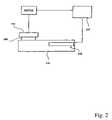
- FIG. 2depicts a block diagram of a metrology system that can be used in conjunction with the apparatus FIG. 1 ;
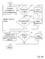
- FIG. 3illustrates at least one example of the operation of the apparatus of FIG. 1 , during which the qualification or requalification process of at least some embodiments of the present invention may be utilized;
- FIG. 4illustrates at least one example of a polishing process for controlling the apparatus of FIG. 1 ;
- FIG. 5illustrates at least one example of a process utilizable for collecting the qualification characteristics required for use with the qualification process of the present invention
- FIGS. 6 a and 6 billustrate at least one example of a process which utilizes the qualification characteristics from a single wafer to properly qualify a polishing tool
- FIG. 7is a high-level block diagram depicting at least some of the aspects of computing devices contemplated as part of and for use with at least some embodiments of the present invention.
- FIG. 8illustrates one example of a memory medium which may be used for storing a computer implemented process of at least some embodiments of the present invention.
- a techniquefor process-qualifying a semiconductor manufacturing tool using the qualification characteristics from a reduced number of wafers (e.g., in at least some embodiments, a single wafer).
- the present inventioncontemplates measuring one or more qualification characteristics from the wafer using an in situ sensor or metrology device necessary for properly qualifying the tool.
- the manufacturing toolis qualified by adjusting one or more parameters of a recipe in accordance with the qualification characteristics measured from the wafer to target one or more manufacturing tool specifications.
- FIG. 1depicts at least one example of a chemical mechanical planarization (CMP) apparatus 120 utilizable for implementing at least some of the aspects of the present invention.
- Apparatus 120includes a lower machine base 122 with a tabletop 128 mounted thereon and a removable outer cover (not shown).
- the tabletop 128supports a series of polishing stations, including a first polishing station 125 a , a second polishing station 125 b , a third polishing station 125 c , and a transfer station 127 .
- the transfer station 127serves multiple functions, including, for example, receiving individual wafers or substrates 110 from a loading apparatus (not shown), washing the wafers, loading the wafers into carrier heads 180 , receiving the wafers 110 from the carrier heads 180 , washing the wafers 110 again, and transferring the wafers 110 back to the loading apparatus.
- a computer based controller 190is connected to the polishing system or apparatus 120 for instructing the system to perform one or more processing steps on the system, such as polishing or qualification process on apparatus 120 .
- the inventionmay be implemented as a computer program-product for use with a computer system or computer based controller 190 .
- Controller 190may include a CPU 192 , which may be one of any form of computer processors that can be used in an industrial setting for controlling various chambers and subprocessors.
- a memory 194is coupled to the CPU 192 for storing information and instructions to be executed by the CPU 192 .
- Memory 194may take the form of any computer-readable medium, such as, for example, any one or more of readily available memory such as random access memory (RAM), read only memory (ROM), floppy disk, hard disk, or any other form of digital storage, local or remote.
- support circuits 196are coupled to the CPU 192 for supporting the processor in a conventional manner. As will be discussed in greater detail below in conjunction with FIG. 7 , these circuits may include cache, power supplies, clock circuits, input/output circuitry and subsystems, and can include input devices used with controller 190 , such as keyboards, trackballs, a mouse, and display devices, such as computer monitors, printers, and plotters.
- a processfor example the qualification process described below, is generally stored in memory 194 , typically as a software routine.
- the software routinemay also be stored and/or executed by a second CPU (not shown) that is remotely located from the hardware being controlled by the CPU 192 .
- Each polishing stationincludes a rotatable platen 130 on which is placed a polishing pad 100 a , 100 b , and 100 c . If wafer 110 is an eight-inch (200 millimeter) or twelve-inch (300 millimeter) diameter disk, then platen 130 and polishing pad 100 will be about twenty or thirty inches in diameter, respectively. Platen 130 may be connected to a platen drive motor (not shown) located inside machine base 122 . For most polishing processes, the platen drive motor rotates platen 130 at thirty to two hundred revolutions per minute, although lower or higher rotational speeds may be used.
- the polishing stations 125 a - 125 cmay include a pad conditioner apparatus 140 .
- Each pad conditioner apparatus 140has a rotatable arm 142 holding an independently rotating conditioner head 144 and an associated washing basin 146 .
- the pad conditioner apparatus 140maintains the condition of the polishing pad so that it will effectively polish the wafers.
- Each polishing stationmay include a conditioning station if the CMP apparatus is used with other pad configurations.
- a slurry 150 containing a reactive agent (e.g., deionized water for oxide polishing) and a chemically-reactive catalyzer (e.g., potassium hydroxide for oxide polishing)may be supplied to the surface of polishing pad 100 by a combined slurry/rinse arm 152 .
- a reactive agente.g., deionized water for oxide polishing
- a chemically-reactive catalyzere.g., potassium hydroxide for oxide polishing
- Slurry/rinse arm 152includes several spray nozzles (not shown) which provide a high-pressure rinse of polishing pad 100 at the end of each polishing and conditioning cycle.
- several intermediate washing stations 155 a , 155 b , and 155 cmay be positioned between adjacent polishing stations 125 a , 125 b , and 125 c to clean wafers as they pass from one station to another.
- the first polishing station 125 ahas a first pad 100 a disposed on platen 130 for removing bulk copper-containing material disposed on the wafer (i.e., a bulk removal polishing platen).
- the second polishing station 125 bhas a second pad 100 b disposed on a platen 130 for polishing a wafer to remove residual copper-containing material disposed on the wafer (i.e., a copper clearing platen).
- a third polishing station 125 c having a third polishing pad 100 cmay be used for a barrier removal polishing process following the two-step copper removal process (i.e., a barrier removal polishing platen).
- a rotatable multi-head carousel 160is positioned above the lower machine base 122 .
- Carousel 160includes four carrier head systems 170 a , 170 b , 170 c , and 170 d .
- Three of the carrier head systemsreceive or hold the wafers 110 by pressing them against the polishing pads 100 a , 100 b , and 100 c , disposed on the polishing stations 125 a - 125 c .
- One of the carrier head systems 170 a - 170 dreceives a wafer 110 from and delivers a wafer 110 to the transfer station 127 .
- the carousel 160is supported by a center post 162 and is rotated about a carousel axis 164 by a motor assembly (not shown) located within the machine base 122 .
- the center post 162also supports a carousel support plate 166 and a cover 188 .
- the four carrier head systems 170 a - 170 dare mounted on the carousel support plate 166 at equal angular intervals about the carousel axis 164 .
- the center post 162allows the carousel motor to rotate the carousel support plate 166 and orbit the carrier head systems 170 a - 170 d about the carousel axis 164 .
- Each carrier head system 170 a - 170 dincludes one carrier head 180 .
- a carrier drive shaft 178connects a carrier head rotation motor 176 to the carrier head 180 so that the carrier head 180 can independently rotate about its own axis.
- each carrier head 180independently oscillates laterally in a radial slot 172 formed in the carousel support plate 166 .
- the carrier head 180performs several mechanical functions. Generally, the carrier head 180 holds the wafer 110 against the polishing pads 100 a , 100 b , and 100 c , evenly distributes a downward pressure across the back surface of the wafer 110 , transfers torque from the drive shaft 178 to the wafer 110 , and ensures that the wafer 110 does not slip out from beneath the carrier head 80 during polishing operations.
- a description of a similar apparatusmay be found in U.S. Pat. No. 6,159,079, the entire disclosure of which is incorporated herein by reference.
- a commercial embodiment of a CMP apparatuscould be, for example, any of a number of processing stations or devices offered by Applied Materials, Inc. of Santa Clara, Calif. including, for example, any number of the MirramesaTM and ReflexionTM line of CMP devices.
- the device depicted in FIG. 1is implemented to perform polishing processes and includes any polishing stations, it is to be understood that the concepts of the present invention may be utilized in conjunction with various other types of semiconductor manufacturing processes and processing resources including for example non-CMP devices, etching tools, deposition tools, plating tools, etc.
- Other examples of processing resourcesinclude polishing stations, chambers, and/or plating cells, and the like.
- FIG. 2depicts a block diagram of a metrology system of a single polishing station (e.g., any one or combination of stations 125 a - 125 c ) of FIG. 1 that may be used in conjunction with the qualification process of the present invention.
- the metrology systemincludes an in situ sensor 210 and a control system 215 .
- In situ sensor 210may be utilized in real time to measure one or more qualification characteristics during execution of the polishing steps of a qualification process, as well as during the polishing steps of an actual production process. As a result, wafers are not required to be removed from the polishing station in order to collect metrology data.
- These qualification characteristicsin turn may be used to qualify a polishing station (e.g., stations 125 a - 125 c ) of the apparatus of FIG. 1 .
- In situ sensor 210may include a wafer thickness measuring device for measuring a topography of the wafer face during polishing. By being able to measure thickness in real-time, in situ sensor 210 is capable of providing a number of qualification characteristics used to properly qualify a semiconductor manufacturing tool. Specific types of in Situ sensors include laser interferometer measuring devices, which employ interference of light waves for purposes of measurement. One example of such an in situ sensor suitable for use with the present invention includes the In Situ Removal Monitor (ISRM) offered by Applied Materials, Inc. of Santa Clara, Calif. Similarly, in situ sensor 210 may include devices for measuring capacitance changes or eddy currents (such as the iScan monitor, also offered by Applied Materials, Inc.
- ISRMIn Situ Removal Monitor
- At least some embodiments of the present inventioncontemplate implementing an in situ sensor capable of measuring both oxide and copper layers.
- Other examples of wafer property measuring devices contemplated by at least some embodiments of the present inventioninclude integrated CD (critical dimension) measurement tools, and tools capable of performing measurements for dishing, erosion and residues, and/or particle monitoring, etc.
- a capacitance or eddy current measuring sensormay be utilized in conjunction with bulk removal polishing station 125 a
- a light wave measuring sensormay be utilized in conjunction with copper clearing station 125 b
- an optical sensormay be utilized in conjunction with barrier removal polishing station 125 c.
- control system 215implements a qualification process for controlling each of the steps required to attain a number of predetermined manufacturing specifications. Specifically, as will be discussed in greater detail below, during the qualification process of the present invention, control system 215 initially directs in situ sensor 210 to gather each of the qualification characteristics required to qualify apparatus 120 from a single wafer. Control system 215 subsequently modifies any number of recipe parameters in order to attain a number of manufacturing specifications (determined according to fab or product demands) associated with apparatus 120 . Thus, control system 215 is operatively coupled to, in addition to in situ sensor 210 , components of apparatus 120 to monitor and control a number of qualification and manufacturing processes.
- in situ sensor 210may be used to obtain various qualification characteristics, for example during qualification procedures, which may be compared against tool specifications to measure the efficiency of the process.
- characteristicsare the removal rate of the film material to be removed from the wafer, the uniformity or nonuniformity in the material removal, the defectivity, and other similar and analogous metrics. These and other characteristics are indicators of the quality of the polishing process.
- the removal rateis mainly used to determine the polishing time of product wafers.
- the nonuniformitydirectly affects the global planarity across the wafer surface, which becomes more important as larger wafers are used in the fabrication of devices.
- the defectivityindicates the number of defects occurring due to for example scratches in the wafer.
- parameterssuch as the applied pressure or downward force, the speed of the polishing table, the speed of the wafer carrier, the slurry composition, the slurry flow, and others, may be modified to adjust the characteristics, in an attempt to satisfy minimum tool specification levels.
- the toolmay require routine forms of maintenance. For example, the polishing pads and other components of the tool may need to be replaced due to normal wear.
- the tooldetermines whether maintenance is necessary by identifying process results that are no longer within minimum specifications (e.g., process drifts). In other cases, the tools may be serviced periodically. In any case, once it is determined that maintenance is necessary (STEP 330 ), the required maintenance is performed (STEP 340 ). For example, the worn polishing pads or other parts may be replaced.
- a new tool recipe for controlling the toolmay be implemented (STEP 350 ).
- the toolmay be directed to produce another product.
- different wafers and substrates, with different characteristics,may be delivered for processing by the tool. Both of these cases (and others) require the implementation of a new recipe.
- the new recipeis downloaded onto the tool (STEP 360 ).
- a first polishing compositionis used with a first polishing pad to remove bulk copper containing material from the wafer surface to substantially planarize the bulk copper containing material (STEP 412 ).
- Bulk removal polishingcontinues until a predetermined amount of copper is removed from the wafer as determined by, for example, an eddy current or capacitance endpoint sensor (or any other analogous or suitable sensor) (STEP 416 ).
- feedback datamay be collected by the sensor for use in optimizing future runs (STEP 414 ). From there, the wafer is delivered to a second or copper clearing polishing platen (e.g., platen 125 b ).
- a second polishing compositionis used with a second polishing pad to remove remaining residual copper containing material (STEP 420 ).
- the residual copper containing material removal processterminates when the underlying barrier layer has been reached (STEP 424 ).
- Thiscan be determined by, for example, an optical or light-sensing metrology device.
- the metrology devicemay be used to collect feedback data for use in optimizing future runs (STEP 422 ).
- the waferis transported to a third or barrier removal polishing platen (e.g., platen 125 c ).
- a third polishing compositionis used with a third polishing pad to remove the barrier layer (STEP 428 ).
- This layeris typically formed on the wafer surface above a dielectric layer. Polishing continues until, for example, the barrier layer, and in some cases a portion of the underlying dielectric, has been removed (STEP 432 ). This can be determined by, for example, an optical sensor and the like. Afterwards, the wafer may be transferred to a cleaning module or subjected to an in situ cleaning process to remove surface defects, or to some other downstream tool for further processing (STEP 436 ).
- the in situ metrology devicesi.e., in situ sensors
- the in situ metrology devicesdescribed above for collecting endpoint and feedback data may be utilized to collect substantially all of the qualification characteristics, during a qualification procedure, required to properly qualify any or all of the platens of the polishing tool, from a single wafer.
- the embodiments of the present inventioncontemplate using a single patterned or production wafer as the source of substantially all of the metrology wafer data required to properly qualify a tool.
- other waferssuch as a single blanket wafer may be used. This is the case because use of the in situ metrology devices or sensors allows measuring of the qualification techniques without removal of the wafer from the tool. As a result, the present invention greatly reduces the time and costs associated with qualifying a polishing tool.
- the qualification characteristics collected from the processing of a single waferis sufficient to properly qualify the polishing tool.
- the waferis premeasured for defects (STEP 504 ).
- the number of defects existing on the wafermay be measured using an optical metrology device or the like.
- the Compass laser-sensing device offered by Applied Materialsmay be utilized.
- a sensor or other metrology devicecollects metrology data from the wafer (STEP 516 ).
- the sensormay be implemented to collect, for example, the thickness of the bulk copper material before and after polishing, as well as a polishing time and the level of current in the material during processing.
- the data measured by the metrology devicealso dictates when to terminate the bulk removal polishing process.
- processingterminates when the measured current drops below or rises above a predetermined level.
- this metrology datais collected and analyzed for purposes of qualifying bulk removal polishing platen 125 a of polishing tool 120 .
- the waferis positioned on copper clearing platen 125 b (STEP 520 ).
- the waferis positioned on copper clearing platen 125 b (STEP 520 ).
- the sensorcollects metrology data from the wafer (STEP 528 ).
- the sensormay be implemented to collect, for example, the polishing time required to clear the copper from the wafer and the level of light intensity in the material during polishing.
- the data measured by this metrology devicealso dictates when to terminate the copper clearing process.
- processingterminates when the intensity of the measured light drops below or rises above a predetermined level.
- this metrology datais collected and analyzed for purposes of qualifying copper clearing platen 125 b of polishing tool 120 .
- the waferis positioned on a barrier removal polishing platen (STEP 532 ).
- barrier layer materialsare removed by polishing the surface of the wafer (STEP 536 ).
- a sensorsuch as an optical sensor or the like, collects metrology data from the wafer (STEP 540 ).
- the sensormay be implemented to collect, for example, the polishing time required to clear the copper from the wafer and the level of light intensity in the material during polishing.
- the data measured by this metrology devicealso dictates when to terminate the barrier removal polishing process.
- processingterminates when the intensity of the measured light drops below or rises above a predetermined level.
- this metrology datais collected and analyzed for purposes of qualifying barrier removal polishing platen 125 c of polishing tool 120 .
- the waferis delivered to a wafer defectivity sensor, where the wafer is measured for defects (STEP 544 ).
- the wafermay be measured for its total number of detects using the metrology device utilized in STEP 504 , as described above.
- the metrology data gathered from a single wafer during the process described in FIG. 5constitutes substantially all of the qualification characteristics required to properly qualify a polishing tool.
- FIGS. 6 a and 6 bOne example of a process that utilizes this data to properly qualify a polishing tool is depicted in FIGS. 6 a and 6 b.
- processingcommences with the calculation of each of the qualification characteristics required to properly qualify bulk removal polishing platen 125 a .
- the raw metrology data measured during processing of the test wafer at the bulk removal polishing platenconstitutes the required qualification data.
- a step of processingmust be performed to convert the raw metrology data into usable form. For example, thickness data at several points may need to be averaged before use.
- the qualification characteristicsmay include a polishing rate and a nonuniformity (although other qualification characteristics are possible).
- the processcalculates the polishing rate and nonuniformity of the platen (STEP 604 ) using the metrology data measured during processing of the test wafer at bulk removal polishing platen 125 a (e.g., STEP 516 ).
- the processutilizes the starting thickness of a bulk material, the ending thickness of the material, and the time required to reach the ending thickness to obtain the polishing rate of the platen.
- the measured metrology datai.e., the film thickness at a number of predetermined points across the wafer
- This profilemay be used to obtain the nonuniformity of the wafer resulting from the bulk removal polishing process.
- the processcompares the qualification characteristics against the minimum tool specifications.
- the processfirst compares the polishing rate against a polishing rate specification for bulk removal polishing platen 125 a (STEP 608 ). If the polishing rate is not within specification, appropriate adjustments are made to the tool recipe so that future runs (i.e., actual production runs) are within specification limits (STEP 612 ). For example if the polishing rate exceeds the specification rate, the bulk removal polishing platen pressure may be reduced.
- the processnext compares the nonuniformity against a specification nonuniformity for the bulk removal polishing platen (STEP 616 ).
- the qualification characteristicsmay take the form of either raw or processed data.
- the qualification characteristicsmay include a polishing rate and a nonuniformity (although other qualification characteristics are possible).
- the processuses the metrology data measured during processing of the test wafer at copper clearing platen 125 b (e.g., STEP 528 ) to calculate the polishing rate and nonuniformity of the platen (STEP 624 ).
- the processutilizes the starting thickness of the copper residue material (as measured, e.g., at the end of the bulk removal qualification process) and the time required to clear the remaining material to determine polishing rate of the platen.
- the change in light intensity taken as a function of timemay be utilized to determine the nonuniformity of the wafer resulting from processing by copper clearing platen 125 b.
- the processcompares the qualification characteristics against minimum tool specifications.
- the processcompares the polishing rate against a polishing rate specification for the copper clearing platen 125 b (STEP 628 ) and the nonuniformity against the nonuniformity specification for the copper clearing platen 125 b (STEP 636 ). If either of these qualification characteristics is not within specification, appropriate adjustments may be made to the tool recipe so that future runs (i.e., actual production runs) are within specification limits (STEP 632 and STEP 640 ). After qualifying copper clearing platen 125 b , qualification shifts to barrier removal polishing platen 125 c.
- the qualification characteristicsmay take the form of either raw or processed data.
- the qualification characteristicsmay include a polishing rate and a nonuniformity (although other qualification characteristics are possible).
- the processuses the metrology data measured during processing of the test wafer at barrier removal polishing platen 125 c (e.g., STEP 540 ) to calculate the polishing rate and nonuniformity of the platen (STEP 644 ).
- the processutilizes the starting thickness of the barrier material (as measured, e.g., at the end of the copper clearing qualification process), the remaining thickness of a dielectric layer (i.e., the layer underlying the barrier layer), and the total polishing time to determine the polishing rate of the platen.
- the processmeasures the thickness of the wafer at a predetermined number of points (e.g., 15-20 points) to determine the nonuniformity of the wafer resulting from barrier removal polishing platen 125 c.
- the processcompares the qualification characteristics against minimum tool specifications.
- the processcompares the polishing rate against a polishing rate specification for barrier removal polishing platen 125 c (STEP 648 ) and the nonuniformity against the nonuniformity specification for barrier removal polishing platen 125 c (STEP 656 ). If either of these qualification characteristics is not within specification, appropriate adjustments may be made to the tool recipe so that future runs (i.e., actual production runs) are within specification limits (STEP 652 and STEP 660 ). After qualifying barrier removal polishing platen 125 c , qualification shifts to defectivity.
- the processcompares the number of defects measured before the polishing (e.g., STEP 504 ) against the number of defects after polishing (e.g., STEP 544 ) (STEP 664 ), and determines whether the change in the number of defects is within specification (STEP 668 ). If the change in the number of defects is within specification, processing ends. However, if the change in the number of defects is not within specification, appropriate adjustments may be made to the tool recipe so that future runs (i.e., actual production runs) are within specification limits (STEP 672 ). For example, the chemical composition of the slurry used in one of the polishing processes may be adjusted. In other embodiments, to qualify the polishing tool for defectivity, instead of analyzing the change in the number of defects, the number of defects measured after polishing (e.g., STEP 544 ) is compared against a specification limit or other requirement.
- FIG. 7illustrates a block diagram of one example of the internal hardware of control system 215 of FIG. 2 , examples of which include any of a number of different types of computers such as those having PentiumTM based processors as manufactured by Intel Corporation of Santa Clara, Calif.
- a bus 756serves as the main information link interconnecting the other components of system 215 .
- CPU 758is the central processing unit of the system, performing calculations and logic operations required to execute the processes of the instant invention as well as other programs.
- Read only memory (ROM) 760 and random access memory (RAM) 762constitute the main memory of the system.
- Disk controller 764interfaces one or more disk drives to the system bus 756 .
- These disk drivesare, for example, floppy disk drives 770 , or CD ROM or DVD (digital video disks) drives 766 , or internal or external hard drives 768 .
- CPU 758can be any number of different types of processors, including those manufactured by Intel Corporation or Motorola of Schaumberg, Ill.
- the memory/storage devicescan be any number of different types of memory devices such as DRAM and SRAM as well as various types of storage devices, including magnetic and optical media. Furthermore, the memory/storage devices can also take the form of a transmission.
- a display interface 772interfaces display 748 and permits information from the bus 756 to be displayed on display 748 .
- Display 748is also an optional accessory.
- Communications with external devicessuch as the other components of the system described above, occur utilizing, for example, communication port 774 .
- port 774may be interfaced with a bus/network linked to CMP device 20 .
- Optical fibers and/or electrical cables and/or conductors and/or optical communicatione.g., infrared, and the like
- wireless communicatione.g., radio frequency (RF), and the like
- Peripheral interface 754interfaces the keyboard 750 and mouse 752 , permitting input data to be transmitted to bus 756 .
- the control systemalso optionally includes an infrared transmitter 778 and/or infrared receiver 776 .
- Infrared transmittersare optionally utilized when the computer system is used in conjunction with one or more of the processing components/stations that transmits/receives data via infrared signal transmission.
- the control systemmay also optionally use a low power radio transmitter 780 and/or a low power radio receiver 782 .
- the low power radio transmittertransmits the signal for reception by components of the production process, and receives signals from the components via the low power radio receiver.
- FIG. 8is an illustration of an exemplary computer readable memory medium 884 utilizable for storing computer readable code or instructions including the model(s), recipe(s), etc).
- medium 884may be used with disk drives illustrated in FIG. 7 .
- memory mediasuch as floppy disks, or a CD ROM, or a digital video disk will contain, for example, a multi-byte locale for a single byte language and the program information for controlling the above system to enable the computer to perform the functions described herein.
- ROM 760 and/or RAM 762can also be used to store the program information that is used to instruct the central processing unit 758 to perform the operations associated with the instant processes.
- suitable computer readable media for storing informationinclude magnetic, electronic, or optical (including holographic) storage, some combination thereof, etc.
- the computer readable mediumcan be a transmission.
- Embodiments of the present inventioncontemplate that various portions of software for implementing the various aspects of the present invention as previously described can reside in the memory/storage devices.
Landscapes
- Engineering & Computer Science (AREA)
- Mechanical Engineering (AREA)
- Mechanical Treatment Of Semiconductor (AREA)
- Finish Polishing, Edge Sharpening, And Grinding By Specific Grinding Devices (AREA)
Abstract
Description
This application is related to and claims the priority of U.S. Provisional Application Ser. No. 60/491,974, filed Aug. 4, 2003, which is incorporated herein by reference.
The present invention relates generally to semiconductor manufacture. More particularly, the present invention relates to techniques for qualifying semiconductor manufacturing tools. Even more specifically, one or more embodiments of the present invention relate to techniques for qualifying a CMP tool using metrology data measured from a single wafer.
In the fabrication of integrated circuits, numerous integrated circuits are typically constructed simultaneously on a single semiconductor wafer. The wafer is then later subjected to a singulation process in which individual integrated circuits are singulated (i.e., extracted) from the wafer.
At certain stages of this fabrication process, it is often necessary to polish a surface of the semiconductor wafer. In general, a semiconductor wafer can be polished to remove high topography, surface defects such as crystal lattice damage, scratches, roughness, or embedded particles of dirt or dust. This polishing process is often referred to as mechanical planarization (MP) and is utilized to improve the quality and reliability of semiconductor stations. In typical situations, these processes are usually performed during the formation of various devices and integrated circuits on the wafer.
The polishing process may also involve the introduction of a chemical slurry (e.g., an alkaline or acidic solution). This polishing process is often referred to as chemical mechanical planarization (CMP). Much like mechanical planarization processes, chemical mechanical polishing is widely used in semiconductor processing operations as a process for planarizing various process layers, e.g., silicon dioxide, which is formed upon a wafer comprised of a semiconducting material, such as silicon. Chemical mechanical polishing operations typically employ an abrasive or abrasive-free slurry distributed to assist in planarizing the surface of a process layer through a combination of mechanical and chemical actions (i.e., the slurry facilitates higher removal rates and selectivity between films of the semiconductor surface).
During the normal course of operation, any number of reasons may necessitate the qualification or re-qualification of these mechanical and chemical mechanical polishing tools. Generally speaking, qualification procedures constitute the process steps required to calibrate and otherwise prepare a tool for production or service (e.g., so that the devices produced by the tool meet minimum predetermined specification requirements, as dictated by the demands of the individual fabs and/or product lines). For example, due to normal wear, a polishing pad may no longer be fit for service, and may need to be replaced by a new pad. In these instances, the qualification procedure collects a number of qualification characteristics (e.g., using the metrology data) measured during initial use of the new pad on sets of blanket or “test” wafers (i.e., wafers having only a thin film of unpatterned material). The qualification procedure then makes appropriate modifications to the tool recipe based on the measured qualification characteristics to ensure that future production runs comport with, for example, a number of minimum specification requirements. In a similar manner, a new tool (e.g., a tool beginning production of a new semiconductor product line) must also be qualified before it can be put into production.
Conventional methods for process-qualifying the above-described tools consume a large numbers of test wafers (approximately 10 to 15 test wafers) and require lengthy amounts of time. With regard to the large amount of time required, this is due to the nature of the stand-alone sensors and metrology devices (i.e., metrology devices that are separate from the tools) used to collect the required qualification characteristics. In particular, because the sensors are separate from the processing tools, in order to collect the qualification characteristics, a typical process first requires measuring preprocessing characteristics followed by physically moving a wafer into the processing tool, where the wafer is processed. After processing, the wafer is removed from the tool and returned to the metrology device, where post-processing characteristics are measured and used in conjunction with the preprocessing characteristics to obtain the characteristics used in qualifying the tool (i.e., the qualification characteristics).
With these conventional methods, the amount of time required to move the wafers back and forth between the tools and the metrology devices is significant. Furthermore, with tools having multiple components or chambers with each requiring qualification, it was more efficient to qualify the chambers in parallel, thus resulting in the consumption of additional wafers. To illustrate, the convention methods may use one wafer to qualify a first chamber or first tool component, a second wafer to qualify a second chamber or second tool component, and a third wafer to qualify a third chamber or third tool component.
In addition to the test wafers, conventional methods often require the testing of a “look-ahead” or patterned production wafer. The testing of these look ahead-wafers was used to ensure that the polishing process met specifications under actual production circumstances.
Recently, conventional in situ metrology devices have been able to eliminate the time required by stand-alone sensors to transfer wafers back and forth between the tools and the metrology devices. However, these conventional devices did not necessarily collect the qualification characteristics used to properly qualify a tool. For instance, conventional in situ metrology devices did not measure film thickness, which is used to qualify tools for, for example, nonuniformity and polishing rate. Consequently, conventional techniques were still required to qualify tools (such as polishing tools) requiring such measurements.
One of the disadvantages of conventional qualification procedures is the cost associated with the testing of these large amounts of blanket and test wafers. In addition to the cost of the test wafers, there is a significant time penalty associated with the qualification procedures. That is, the tools cannot be used to produce products during the qualification process. Furthermore, the processing of test wafers subtracts from the useful life of the polishing pads, since they have only a finite amount of polishing cycles before requiring a change.
Accordingly, increasingly efficient techniques for qualifying such polishing processes are needed. Specifically, what is required is a technique that greatly reduces the number of wafers required for properly qualifying a polishing process. In this manner, the cost and time associated with obtaining a production-ready polishing process may be minimized.
The present invention addresses the needs and the problems described above by providing a technique for process qualifying a semiconductor manufacturing tool using qualification characteristics measured from a reduced number of wafers (e.g., in at least some embodiments, a single wafer). In at least some embodiments, the technique commences during the processing of a wafer with the manufacturing tool. During processing, the technique involves using an in situ metrology device able to measure from the wafer one or more qualification characteristics required to properly qualify the tool (e.g., wafer thickness information). Thus, wafers need not be transferred from the tool in order to collect qualification characteristics. Subsequently, the manufacturing tool is qualified by adjusting one or more parameters of a recipe in accordance with the qualification characteristics measured from the wafer to target one or more manufacturing tool specifications.
In one or more parallel and at least somewhat overlapping embodiments, the tool to be qualified includes a bulk removal polishing platen, a copper clearing platen and a barrier removal polishing platen. In these cases, the technique involves transferring a wafer to each of the bulk removal polishing, copper clearing and barrier removal polishing platens, where qualification characteristics are measured during wafer processing. These platens are subsequently qualified by adjusting one or more parameters of a recipe associated with each platen in accordance with the qualification characteristics measured from the wafer, to target one or more platen specifications.
In one or more other parallel and at least somewhat overlapping embodiments, the technique involves measuring a defectivity from the wafer during processing. Subsequently, the technique qualifies the tool for detectivity by adjusting one or more parameters of the recipe in accordance with the defectivity measured during processing to target a defectivity specification.
Various objects, features, and advantages of the present invention can be more fully appreciated as the same become better understood with reference to the following detailed description of the present invention when considered in connection with the accompanying drawings, in which:
In accordance with at least some embodiments of the present invention, a technique is provided for process-qualifying a semiconductor manufacturing tool using the qualification characteristics from a reduced number of wafers (e.g., in at least some embodiments, a single wafer). Specifically, during processing of a wafer by the tool, the present invention contemplates measuring one or more qualification characteristics from the wafer using an in situ sensor or metrology device necessary for properly qualifying the tool. Subsequently, the manufacturing tool is qualified by adjusting one or more parameters of a recipe in accordance with the qualification characteristics measured from the wafer to target one or more manufacturing tool specifications.
A computer basedcontroller 190 is connected to the polishing system orapparatus 120 for instructing the system to perform one or more processing steps on the system, such as polishing or qualification process onapparatus 120. The invention may be implemented as a computer program-product for use with a computer system or computer basedcontroller 190.Controller 190 may include aCPU 192, which may be one of any form of computer processors that can be used in an industrial setting for controlling various chambers and subprocessors. Amemory 194 is coupled to theCPU 192 for storing information and instructions to be executed by theCPU 192.Memory 194, may take the form of any computer-readable medium, such as, for example, any one or more of readily available memory such as random access memory (RAM), read only memory (ROM), floppy disk, hard disk, or any other form of digital storage, local or remote. In addition, support circuits196 are coupled to theCPU 192 for supporting the processor in a conventional manner. As will be discussed in greater detail below in conjunction withFIG. 7 , these circuits may include cache, power supplies, clock circuits, input/output circuitry and subsystems, and can include input devices used withcontroller 190, such as keyboards, trackballs, a mouse, and display devices, such as computer monitors, printers, and plotters.
A process, for example the qualification process described below, is generally stored inmemory 194, typically as a software routine. The software routine may also be stored and/or executed by a second CPU (not shown) that is remotely located from the hardware being controlled by theCPU 192.
Each polishing station includes arotatable platen 130 on which is placed apolishing pad wafer 110 is an eight-inch (200 millimeter) or twelve-inch (300 millimeter) diameter disk, then platen130 and polishingpad 100 will be about twenty or thirty inches in diameter, respectively.Platen 130 may be connected to a platen drive motor (not shown) located insidemachine base 122. For most polishing processes, the platen drive motor rotatesplaten 130 at thirty to two hundred revolutions per minute, although lower or higher rotational speeds may be used.
The polishing stations125a-125cmay include apad conditioner apparatus 140. Eachpad conditioner apparatus 140 has arotatable arm 142 holding an independently rotatingconditioner head 144 and an associatedwashing basin 146. Thepad conditioner apparatus 140 maintains the condition of the polishing pad so that it will effectively polish the wafers. Each polishing station may include a conditioning station if the CMP apparatus is used with other pad configurations.
Aslurry 150 containing a reactive agent (e.g., deionized water for oxide polishing) and a chemically-reactive catalyzer (e.g., potassium hydroxide for oxide polishing) may be supplied to the surface of polishingpad 100 by a combined slurry/rinsearm 152. If polishingpad 100 is a standard pad,slurry 150 may also include abrasive particles (e.g., silicon dioxide for oxide polishing). Typically, sufficient slurry is provided to cover and wet theentire polishing pad 100. Slurry/rinsearm 152 includes several spray nozzles (not shown) which provide a high-pressure rinse ofpolishing pad 100 at the end of each polishing and conditioning cycle. Furthermore, severalintermediate washing stations stations
In at least one embodiment of the present invention, thefirst polishing station 125ahas afirst pad 100adisposed onplaten 130 for removing bulk copper-containing material disposed on the wafer (i.e., a bulk removal polishing platen). Thesecond polishing station 125bhas a second pad100bdisposed on aplaten 130 for polishing a wafer to remove residual copper-containing material disposed on the wafer (i.e., a copper clearing platen). Athird polishing station 125chaving athird polishing pad 100cmay be used for a barrier removal polishing process following the two-step copper removal process (i.e., a barrier removal polishing platen).
A rotatablemulti-head carousel 160 is positioned above thelower machine base 122.Carousel 160 includes fourcarrier head systems wafers 110 by pressing them against the polishingpads carrier head systems 170a-170dreceives awafer 110 from and delivers awafer 110 to thetransfer station 127. Thecarousel 160 is supported by acenter post 162 and is rotated about acarousel axis 164 by a motor assembly (not shown) located within themachine base 122. Thecenter post 162 also supports acarousel support plate 166 and acover 188.
The fourcarrier head systems 170a-170dare mounted on thecarousel support plate 166 at equal angular intervals about thecarousel axis 164. Thecenter post 162 allows the carousel motor to rotate thecarousel support plate 166 and orbit thecarrier head systems 170a-170dabout thecarousel axis 164. Eachcarrier head system 170a-170dincludes onecarrier head 180. Acarrier drive shaft 178 connects a carrierhead rotation motor 176 to thecarrier head 180 so that thecarrier head 180 can independently rotate about its own axis. There is onecarrier drive shaft 178 andmotor 176 for eachhead 180. In addition, eachcarrier head 180 independently oscillates laterally in aradial slot 172 formed in thecarousel support plate 166.
Thecarrier head 180 performs several mechanical functions. Generally, thecarrier head 180 holds thewafer 110 against the polishingpads wafer 110, transfers torque from thedrive shaft 178 to thewafer 110, and ensures that thewafer 110 does not slip out from beneath the carrier head80 during polishing operations.
A description of a similar apparatus may be found in U.S. Pat. No. 6,159,079, the entire disclosure of which is incorporated herein by reference. A commercial embodiment of a CMP apparatus could be, for example, any of a number of processing stations or devices offered by Applied Materials, Inc. of Santa Clara, Calif. including, for example, any number of the Mirramesa™ and Reflexion™ line of CMP devices. Also, while the device depicted inFIG. 1 is implemented to perform polishing processes and includes any polishing stations, it is to be understood that the concepts of the present invention may be utilized in conjunction with various other types of semiconductor manufacturing processes and processing resources including for example non-CMP devices, etching tools, deposition tools, plating tools, etc. Other examples of processing resources include polishing stations, chambers, and/or plating cells, and the like.
Insitu sensor 210 may include a wafer thickness measuring device for measuring a topography of the wafer face during polishing. By being able to measure thickness in real-time, insitu sensor 210 is capable of providing a number of qualification characteristics used to properly qualify a semiconductor manufacturing tool. Specific types of in Situ sensors include laser interferometer measuring devices, which employ interference of light waves for purposes of measurement. One example of such an in situ sensor suitable for use with the present invention includes the In Situ Removal Monitor (ISRM) offered by Applied Materials, Inc. of Santa Clara, Calif. Similarly, insitu sensor 210 may include devices for measuring capacitance changes or eddy currents (such as the iScan monitor, also offered by Applied Materials, Inc. of Santa Clara, Calif.), optical sensors (such as the Nanospec series of metrology devices offered by Nanometrics of Milpitas, Calif. or Nova 2020 offered by Nova Measuring Instruments, Ltd. of Rehovot, Israel), devices for measuring frictional changes, and acoustic mechanisms for measuring wave propagation (as films and layers are removed during polishing), all of which may be used to detect thickness in real time. Furthermore, it should be noted that at least some embodiments of the present invention contemplate implementing an in situ sensor capable of measuring both oxide and copper layers. Other examples of wafer property measuring devices contemplated by at least some embodiments of the present invention include integrated CD (critical dimension) measurement tools, and tools capable of performing measurements for dishing, erosion and residues, and/or particle monitoring, etc.
Any combination of the above sensors may be utilized with the present invention. For instance, in the example ofFIG. 1 , a capacitance or eddy current measuring sensor may be utilized in conjunction with bulkremoval polishing station 125a, a light wave measuring sensor may be utilized in conjunction withcopper clearing station 125b, and an optical sensor may be utilized in conjunction with barrierremoval polishing station 125c.
Referring back toFIG. 2 , in accordance with at least some of the embodiments of the present invention,control system 215 implements a qualification process for controlling each of the steps required to attain a number of predetermined manufacturing specifications. Specifically, as will be discussed in greater detail below, during the qualification process of the present invention,control system 215 initially directs insitu sensor 210 to gather each of the qualification characteristics required to qualifyapparatus 120 from a single wafer.Control system 215 subsequently modifies any number of recipe parameters in order to attain a number of manufacturing specifications (determined according to fab or product demands) associated withapparatus 120. Thus,control system 215 is operatively coupled to, in addition to insitu sensor 210, components ofapparatus 120 to monitor and control a number of qualification and manufacturing processes.
As mentioned above, insitu sensor 210 may be used to obtain various qualification characteristics, for example during qualification procedures, which may be compared against tool specifications to measure the efficiency of the process. Examples of such characteristics are the removal rate of the film material to be removed from the wafer, the uniformity or nonuniformity in the material removal, the defectivity, and other similar and analogous metrics. These and other characteristics are indicators of the quality of the polishing process. The removal rate is mainly used to determine the polishing time of product wafers. The nonuniformity directly affects the global planarity across the wafer surface, which becomes more important as larger wafers are used in the fabrication of devices. The defectivity indicates the number of defects occurring due to for example scratches in the wafer. Each of the above depends on and may be affected by the polishing parameters of the process recipe. Thus, parameters such as the applied pressure or downward force, the speed of the polishing table, the speed of the wafer carrier, the slurry composition, the slurry flow, and others, may be modified to adjust the characteristics, in an attempt to satisfy minimum tool specification levels.
During the normal course of operation, the tool may require routine forms of maintenance. For example, the polishing pads and other components of the tool may need to be replaced due to normal wear. In some cases, the tool determines whether maintenance is necessary by identifying process results that are no longer within minimum specifications (e.g., process drifts). In other cases, the tools may be serviced periodically. In any case, once it is determined that maintenance is necessary (STEP330), the required maintenance is performed (STEP340). For example, the worn polishing pads or other parts may be replaced.
In other instances, a new tool recipe for controlling the tool may be implemented (STEP350). For example, the tool may be directed to produce another product. Similarly, different wafers and substrates, with different characteristics, may be delivered for processing by the tool. Both of these cases (and others) require the implementation of a new recipe. Whatever the case, the new recipe is downloaded onto the tool (STEP360).
In each of the above (and other) situations, the tool must be requalified before production can recommence (STEP310). As discussed, the qualification procedure ensures that the results of processing by the tool meet a number of minimum specification levels. Once qualified, the tool recommences the processing of wafers (STEP320).
As discussed, the qualification procedure of the present invention is utilizable with a multi-step polishing process for removing conductive materials and conductive material residues from a wafer or substrate surface using one or more polishing pads. One example of such a polishing processes is described with reference toFIG. 4 . Initially, a wafer is transferred from an upstream tool to the polishing tool (STEP404). In the example ofFIG. 1 , the wafer may be transferred from an electrochemical plating (ECP) tool to bulkremoval polishing platen 125aoftool 120. Subsequently, a tool recipe for controlling the polishing tool is downloaded and implemented on the tool (STEP408).
At the bulk removal polishing platen, a first polishing composition is used with a first polishing pad to remove bulk copper containing material from the wafer surface to substantially planarize the bulk copper containing material (STEP412). Bulk removal polishing continues until a predetermined amount of copper is removed from the wafer as determined by, for example, an eddy current or capacitance endpoint sensor (or any other analogous or suitable sensor) (STEP416). In addition, feedback data may be collected by the sensor for use in optimizing future runs (STEP414). From there, the wafer is delivered to a second or copper clearing polishing platen (e.g.,platen 125b).
At the copper clearing platen, a second polishing composition is used with a second polishing pad to remove remaining residual copper containing material (STEP420). The residual copper containing material removal process terminates when the underlying barrier layer has been reached (STEP424). This can be determined by, for example, an optical or light-sensing metrology device. In addition, the metrology device may be used to collect feedback data for use in optimizing future runs (STEP422). Subsequently, the wafer is transported to a third or barrier removal polishing platen (e.g.,platen 125c).
At the barrier removal polishing platen, a third polishing composition is used with a third polishing pad to remove the barrier layer (STEP428). This layer is typically formed on the wafer surface above a dielectric layer. Polishing continues until, for example, the barrier layer, and in some cases a portion of the underlying dielectric, has been removed (STEP432). This can be determined by, for example, an optical sensor and the like. Afterwards, the wafer may be transferred to a cleaning module or subjected to an in situ cleaning process to remove surface defects, or to some other downstream tool for further processing (STEP436).
As discussed above, maintenance (e.g., pad replacement at any or all of the above-described platens) requires the requalification of the polishing tool. In accordance with at least some of the concepts of the present invention, and as will be discussed in greater detail below, the in situ metrology devices (i.e., in situ sensors) described above for collecting endpoint and feedback data may be utilized to collect substantially all of the qualification characteristics, during a qualification procedure, required to properly qualify any or all of the platens of the polishing tool, from a single wafer. Specifically, at least some of the embodiments of the present invention contemplate using a single patterned or production wafer as the source of substantially all of the metrology wafer data required to properly qualify a tool. In other embodiments, other wafers, such as a single blanket wafer may be used. This is the case because use of the in situ metrology devices or sensors allows measuring of the qualification techniques without removal of the wafer from the tool. As a result, the present invention greatly reduces the time and costs associated with qualifying a polishing tool.
Referring now toFIG. 5 , at least one example of a process utilizable for collecting the necessary qualification characteristics is described. As discussed, the qualification characteristics collected from the processing of a single wafer is sufficient to properly qualify the polishing tool. Initially, after receiving the wafer attool 120, the wafer is premeasured for defects (STEP504). Specifically, the number of defects existing on the wafer may be measured using an optical metrology device or the like. For example, the Compass laser-sensing device offered by Applied Materials may be utilized.
Subsequently, the wafer is positioned on bulkremoval polishing platen 125a(STEP508). Bulk copper containing materials are then removed by polishing the surface of the wafer (STEP512). In conjunction with the bulk removal polishing procedure, a sensor or other metrology device (e.g., in situ sensor210) collects metrology data from the wafer (STEP516). In particular, the sensor may be implemented to collect, for example, the thickness of the bulk copper material before and after polishing, as well as a polishing time and the level of current in the material during processing. In addition, the data measured by the metrology device also dictates when to terminate the bulk removal polishing process. For example, in the case of an eddy current sensor, which is capable of using current changes to detect changes in film characteristics (e.g., changes in film characteristics, such as thickness, directly affect a current), processing terminates when the measured current drops below or rises above a predetermined level. As will be discussed in greater detail below, this metrology data is collected and analyzed for purposes of qualifying bulkremoval polishing platen 125aof polishingtool 120.
After the bulk removal polishing process has been completed, the wafer is positioned oncopper clearing platen 125b(STEP520). At the copper clearing platen, residual copper containing materials are removed by polishing the surface of the wafer (STEP520). In conjunction with the copper clearing procedure, a sensor such as the ISRM collects metrology data from the wafer (STEP528). In particular, the sensor may be implemented to collect, for example, the polishing time required to clear the copper from the wafer and the level of light intensity in the material during polishing. As with the bulk removal polishing platen, the data measured by this metrology device also dictates when to terminate the copper clearing process. For example, in the case of an optical sensor, which is capable of detecting changes in light intensity (e.g., a change from copper film to a barrier material directly affects light intensity), processing terminates when the intensity of the measured light drops below or rises above a predetermined level. As will be discussed in greater detail below, this metrology data is collected and analyzed for purposes of qualifyingcopper clearing platen 125bof polishingtool 120.
After the copper clearing process has been completed, the wafer is positioned on a barrier removal polishing platen (STEP532). At the barrier removal polishing platen, barrier layer materials are removed by polishing the surface of the wafer (STEP536). In conjunction with this procedure, a sensor, such as an optical sensor or the like, collects metrology data from the wafer (STEP540). In particular, the sensor may be implemented to collect, for example, the polishing time required to clear the copper from the wafer and the level of light intensity in the material during polishing. As with the previous platens, the data measured by this metrology device also dictates when to terminate the barrier removal polishing process. For example, in the case of an optical sensor, which is capable of detecting a change in light intensity (e.g., a change from barrier material to a dielectric material directly affects light intensity), processing terminates when the intensity of the measured light drops below or rises above a predetermined level. As will be discussed in greater detail below, this metrology data is collected and analyzed for purposes of qualifying barrierremoval polishing platen 125cof polishingtool 120.
After wafer polishing has been completed, the wafer is delivered to a wafer defectivity sensor, where the wafer is measured for defects (STEP544). For example, the wafer may be measured for its total number of detects using the metrology device utilized inSTEP 504, as described above.
In accordance with at least some of the concepts of the present invention, the metrology data gathered from a single wafer during the process described inFIG. 5 (STEPS FIGS. 6 aand6b.
Referring toFIGS. 6 aand6b, processing commences with the calculation of each of the qualification characteristics required to properly qualify bulkremoval polishing platen 125a. In at least some embodiments, the raw metrology data measured during processing of the test wafer at the bulk removal polishing platen constitutes the required qualification data. In other cases, a step of processing must be performed to convert the raw metrology data into usable form. For example, thickness data at several points may need to be averaged before use. In at least some embodiments of the present invention, the qualification characteristics may include a polishing rate and a nonuniformity (although other qualification characteristics are possible). In these cases, the process calculates the polishing rate and nonuniformity of the platen (STEP604) using the metrology data measured during processing of the test wafer at bulkremoval polishing platen 125a(e.g., STEP516). Specifically, the process utilizes the starting thickness of a bulk material, the ending thickness of the material, and the time required to reach the ending thickness to obtain the polishing rate of the platen. Similarly, the measured metrology data (i.e., the film thickness at a number of predetermined points across the wafer) may be utilized to generate a wafer profile. This profile, in turn may be used to obtain the nonuniformity of the wafer resulting from the bulk removal polishing process.
From there, the process compares the qualification characteristics against the minimum tool specifications. Thus, the process first compares the polishing rate against a polishing rate specification for bulkremoval polishing platen 125a(STEP608). If the polishing rate is not within specification, appropriate adjustments are made to the tool recipe so that future runs (i.e., actual production runs) are within specification limits (STEP612). For example if the polishing rate exceeds the specification rate, the bulk removal polishing platen pressure may be reduced. After qualifying bulkremoval polishing platen 125afor its polishing rate, the process next compares the nonuniformity against a specification nonuniformity for the bulk removal polishing platen (STEP616). If the nonuniformity is not within specification, appropriate adjustments are made to the tool recipe so that future runs (i.e., actual production runs) are within specification limits (STEP620). For example, the polishing pressures applied by various zones in a polishing head to the wafer may be adjusted. Similarly, the slurry composition used in the bulk removal polishing process may be adjusted. As known by those of ordinary skill in the art, the exact adjustments made by the process to comport with tool specifications may be determined in view of, for example, design of experiments (DOE) information and other similar data. After qualifying bulkremoval polishing platen 125afor nonuniformity, qualification shifts tocopper clearing platen 125b.
Processing continues with the calculation of each of the qualification characteristics necessary to properly qualifycopper clearing platen 125b. As with the bulk removal polishing qualification procedure, the qualification characteristics may take the form of either raw or processed data. In at least some embodiments of the present invention, the qualification characteristics may include a polishing rate and a nonuniformity (although other qualification characteristics are possible). In these cases, the process uses the metrology data measured during processing of the test wafer atcopper clearing platen 125b(e.g., STEP528) to calculate the polishing rate and nonuniformity of the platen (STEP624). Specifically, the process utilizes the starting thickness of the copper residue material (as measured, e.g., at the end of the bulk removal qualification process) and the time required to clear the remaining material to determine polishing rate of the platen. The change in light intensity taken as a function of time (measured by the copper clearing platen metrology device) may be utilized to determine the nonuniformity of the wafer resulting from processing bycopper clearing platen 125b.
Subsequently, the process compares the qualification characteristics against minimum tool specifications. Thus, the process compares the polishing rate against a polishing rate specification for thecopper clearing platen 125b(STEP628) and the nonuniformity against the nonuniformity specification for thecopper clearing platen 125b(STEP636). If either of these qualification characteristics is not within specification, appropriate adjustments may be made to the tool recipe so that future runs (i.e., actual production runs) are within specification limits (STEP 632 and STEP640). After qualifyingcopper clearing platen 125b, qualification shifts to barrierremoval polishing platen 125c.
Processing continues with the calculation of each of the qualification characteristics necessary to properly qualify barrierremoval polishing platen 125c. As with the above, the qualification characteristics may take the form of either raw or processed data. In at least some embodiments of the present invention, the qualification characteristics may include a polishing rate and a nonuniformity (although other qualification characteristics are possible). In these cases, the process uses the metrology data measured during processing of the test wafer at barrierremoval polishing platen 125c(e.g., STEP540) to calculate the polishing rate and nonuniformity of the platen (STEP644). Specifically, the process utilizes the starting thickness of the barrier material (as measured, e.g., at the end of the copper clearing qualification process), the remaining thickness of a dielectric layer (i.e., the layer underlying the barrier layer), and the total polishing time to determine the polishing rate of the platen. Similarly, the process measures the thickness of the wafer at a predetermined number of points (e.g., 15-20 points) to determine the nonuniformity of the wafer resulting from barrierremoval polishing platen 125c.
Subsequently, the process compares the qualification characteristics against minimum tool specifications. Thus, the process compares the polishing rate against a polishing rate specification for barrierremoval polishing platen 125c(STEP648) and the nonuniformity against the nonuniformity specification for barrierremoval polishing platen 125c(STEP656). If either of these qualification characteristics is not within specification, appropriate adjustments may be made to the tool recipe so that future runs (i.e., actual production runs) are within specification limits (STEP 652 and STEP660). After qualifying barrierremoval polishing platen 125c, qualification shifts to defectivity.
To qualify the polishing tool for defectivity, the process compares the number of defects measured before the polishing (e.g., STEP504) against the number of defects after polishing (e.g., STEP544) (STEP664), and determines whether the change in the number of defects is within specification (STEP668). If the change in the number of defects is within specification, processing ends. However, if the change in the number of defects is not within specification, appropriate adjustments may be made to the tool recipe so that future runs (i.e., actual production runs) are within specification limits (STEP672). For example, the chemical composition of the slurry used in one of the polishing processes may be adjusted. In other embodiments, to qualify the polishing tool for defectivity, instead of analyzing the change in the number of defects, the number of defects measured after polishing (e.g., STEP544) is compared against a specification limit or other requirement.
As discussed above, the qualification process of the present invention may be implemented in any computer system or computer-based controller. One example of such a system is described in greater detail below with reference toFIG. 7 . Specifically,FIG. 7 illustrates a block diagram of one example of the internal hardware ofcontrol system 215 ofFIG. 2 , examples of which include any of a number of different types of computers such as those having Pentium™ based processors as manufactured by Intel Corporation of Santa Clara, Calif. Abus 756 serves as the main information link interconnecting the other components ofsystem 215.CPU 758 is the central processing unit of the system, performing calculations and logic operations required to execute the processes of the instant invention as well as other programs. Read only memory (ROM)760 and random access memory (RAM)762 constitute the main memory of the system.Disk controller 764 interfaces one or more disk drives to thesystem bus 756. These disk drives are, for example,floppy disk drives 770, or CD ROM or DVD (digital video disks) drives766, or internal or externalhard drives 768.CPU 758 can be any number of different types of processors, including those manufactured by Intel Corporation or Motorola of Schaumberg, Ill. The memory/storage devices can be any number of different types of memory devices such as DRAM and SRAM as well as various types of storage devices, including magnetic and optical media. Furthermore, the memory/storage devices can also take the form of a transmission.
Adisplay interface 772interfaces display 748 and permits information from thebus 756 to be displayed ondisplay 748.Display 748 is also an optional accessory. Communications with external devices such as the other components of the system described above, occur utilizing, for example,communication port 774. For example,port 774 may be interfaced with a bus/network linked to CMP device20. Optical fibers and/or electrical cables and/or conductors and/or optical communication (e.g., infrared, and the like) and/or wireless communication (e.g., radio frequency (RF), and the like) can be used as the transport medium between the external devices andcommunication port 774.Peripheral interface 754 interfaces thekeyboard 750 andmouse 752, permitting input data to be transmitted tobus 756. In addition to these components, the control system also optionally includes an infrared transmitter778 and/or infrared receiver776. Infrared transmitters are optionally utilized when the computer system is used in conjunction with one or more of the processing components/stations that transmits/receives data via infrared signal transmission. Instead of utilizing an infrared transmitter or infrared receiver, the control system may also optionally use a lowpower radio transmitter 780 and/or a lowpower radio receiver 782. The low power radio transmitter transmits the signal for reception by components of the production process, and receives signals from the components via the low power radio receiver.
Embodiments of the present invention contemplate that various portions of software for implementing the various aspects of the present invention as previously described can reside in the memory/storage devices.
In general, it should be emphasized that the various components of embodiments of the present invention can be implemented in hardware, software, or a combination thereof. In such embodiments, the various components and steps would be implemented in hardware and/or software to perform the functions of the present invention. Any presently available or future developed computer software language and/or hardware components can be employed in such embodiments of the present invention. For example, at least some of the functionality mentioned above could be implemented using C or C++ programming languages.
It is also to be appreciated and understood that the specific embodiments of the invention described hereinbefore are merely illustrative of the general principles of the invention. Various modifications may be made by those skilled in the art consistent with the principles set forth hereinbefore.
Claims (39)
1. A method for qualifying a semiconductor manufacturing tool comprising a bulk removal polishing platen, a copper clearing platen and a barrier removal polishing platen, said method comprising:
(a) transferring a wafer to said bulk removal polishing platen;
(b) measuring, in situ, bulk removal polishing platen qualification characteristics from said wafer during processing by said bulk removal polishing platen;
(c) qualifying said bulk removal polishing platen by adjusting one or more parameters of a process recipe in accordance with said one or more bulk removal polishing platen qualification characteristics measured from said wafer to target one or more bulk removal polishing platen specifications;
(d) transferring a wafer to said copper clearing platen;
(e) measuring, in situ, copper clearing platen qualification characteristics from said wafer during processing by said copper clearing platen;
(f) qualifying said copper clearing platen by adjusting one or more parameters of said recipe revised in (c) in accordance with said one or more copper clearing platen qualification characteristics measured from said wafer to target one or more copper clearing platen specifications;
(g) transferring a wafer to said barrier removal polishing platen;
(h) measuring, in situ, barrier removal polishing platen qualification characteristics from said wafer during processing by said barrier removal polishing platen;
(i) qualifying said barrier removal polishing platen by adjusting one or more parameters of said recipe revised in (f) in accordance with said one or more barrier removal polishing platen qualification characteristics to target one or more barrier removal polishing platen specifications;
(j) using said recipe revised in (i) in the processing of one or more subsequent wafers by each of said bulk removal polishing platen, said copper clearing platen, and said barrier removal polishing platen;
(k) measuring, in situ, a defectivity from said wafer; and
(l) qualifying said tool for defectivity by adjusting one or more parameters of said recipe in accordance with said defectivity to target a defectivity specification.
2. The method ofclaim 1 ,
wherein said bulk removal polishing platen is qualified by adjusting one or more parameters of a first recipe;
wherein said copper clearing platen is qualified by adjusting one or more parameters of a second recipe;
wherein said barrier removal polishing platen, is qualified by adjusting one or more parameters of a third recipe; and
wherein said first, second, and third recipes are distinct.
3. The method ofclaim 1 , wherein steps (a)-(j) are performed periodically.
4. A method for qualifying a semiconductor manufacturing tool comprising a set of polishing and clearing platens, said method comprising:
(a) processing a wafer with the set of platens of said manufacturing tool;
(b) measuring, in situ, from said wafer, during processing by each of the set of platens of said manufacturing tool, one or more qualification characteristics of each of the set of platens, wherein said one or more qualification characteristics include a defectivity;
(c) after measuring qualification characteristics of one of the set of platens, qualifying the one of the set of platens of said manufacturing tool by adjusting one or more parameters of a process recipe in accordance with said one or more qualification characteristics measured from said wafer to target one or more specifications of the one of the set of platens;
(d) repeating the adjustment of parameters of the recipe while qualifying each other of the set of platens, to provide a final recipe; and
(e) using said final recipe in the processing of one or more subsequent wafers by each of the set of platens of said manufacturing tool.
5. The method ofclaim 4 , wherein said manufacturing tool comprises a chemical planarization tool, which further comprises a bulk copper removal polishing platen, and wherein said one or more qualification parameters are measured during processing by said bulk copper removal polishing platen.
6. The method ofclaim 4 , wherein said manufacturing tool comprises a chemical planarization tool, which further comprises a copper clearing platen, and wherein said one or more qualification parameters are measured during processing by said copper clearing platen.
7. The method ofclaim 4 , wherein said manufacturing tool comprises a chemical planarization tool, which further comprises a barrier removal polishing platen, and wherein said one or more qualification parameters are measured during processing by said barrier removal polishing platen.
8. The method ofclaim 4 , wherein said manufacturing tool comprises a chemical planarization tool, which further comprises a bulk copper removal polishing platen and a copper clearing platen, and wherein said one or more qualification parameters are measured during processing by said bulk copper removal polishing platen and said copper clearing platen.
9. The method ofclaim 4 , wherein said manufacturing tool comprises a chemical planarization tool, which further comprises a copper clearing platen and a barrier removal polishing platen, and wherein said one or more qualification parameters are measured during processing by said copper clearing platen and said barrier removal polishing platen.
10. The method ofclaim 4 , wherein said manufacturing tool comprises a chemical planarization tool, which further comprises a bulk copper removal polishing platen, a copper clearing platen, and a barrier removal polishing platen, and wherein said one or more qualification parameters are measured during processing by said bulk copper removal polishing platen, said copper clearing platen, and said barrier removal polishing platen.
11. The method ofclaim 4 , wherein said measuring comprises measuring using an in situ eddy current measuring sensor implemented at a bulk removal polishing platen of said manufacturing tool.
12. The method ofclaim 4 , wherein said measuring comprises measuring using an in situ laser interferometer implemented at a copper clearing platen of said manufacturing tool.
13. The method ofclaim 4 , wherein said measuring comprises measuring using an in situ optical sensor implemented at a barrier removal polishing platen of said manufacturing tool.
14. The method ofclaim 4 , where said one or more qualification characteristics comprises a polishing rate.
15. The method ofclaim 4 , where said one or more qualification characteristics comprises a nonuniformity.
16. The method ofclaim 4 , wherein said wafer comprises a single patterned wafer.
17. The method ofclaim 16 , wherein all of said one or more qualification characteristics required to properly qualify said tool are measured from said single patterned wafer.
18. The method ofclaim 4 , wherein said tool is properly qualified using qualification characteristics measured only from said wafer.
19. A semiconductor manufacturing tool including a set of polishing and clearing platens, the tool comprising:
a processing module at each of the set of platens capable of processing a wafer;
an in situ metrology device at each of the set of platens capable of measuring from said wafer, during processing by each of the set of platens, one or more qualification characteristics of each of the set of platens, wherein said one or more qualification characteristics include a defectivity; and
a controller at each of the set of platens capable of qualifying said each of the set of platens by adjusting one or more parameters of a process recipe in accordance with said one or more qualification characteristics measured from said wafer to target one or more specifications of corresponding platens, wherein a resulting recipe is used in the processing of one or more subsequent wafers by each of the set of platens of said manufacturing tool.
20. The tool ofclaim 19 , wherein said manufacturing tool comprises a chemical planarization tool, wherein said processing module comprises a bulk copper removal polishing platen, and wherein said one or more qualification parameters are measured during processing by said bulk copper removal polishing platen.
21. The tool ofclaim 19 , wherein said manufacturing tool comprises a chemical planarization tool, wherein said processing module comprises a copper clearing platen, and wherein said one or more qualification parameters are measured during processing by said copper clearing platen.
22. The tool ofclaim 19 , wherein said manufacturing tool comprises a chemical planarization tool, wherein said processing module comprises a barrier removal polishing platen, and wherein said one or more qualification parameters are measured during processing by said barrier removal polishing platen.
23. The tool ofclaim 19 , wherein said in situ metrology device comprises an in situ eddy current measuring sensor implemented at a bulk removal polishing platen of said manufacturing tool.
24. The tool ofclaim 19 , wherein said in situ metrology device comprises an in situ laser interferometer implemented at a copper clearing platen of said manufacturing tool.
25. The tool ofclaim 19 , wherein said in situ metrology device comprises an in situ optical sensor implemented at a barrier removal polishing platen of said manufacturing tool.
26. The tool ofclaim 19 , where said one or more qualification characteristics comprises a polishing rate.
27. The tool ofclaim 19 , where said one or more qualification characteristics comprises a nonuniformity.
28. A system for qualifying a semiconductor manufacturing tool comprising a set of polishing and clearing platens, said system comprising:
means for processing a wafer with the set of platens of said manufacturing tool;
means for measuring, in situ, from said wafer, during processing by each of the set of platens of said manufacturing tool, one or more qualification characteristics of each of the set of platens, wherein said one or more qualification characteristics include a defectivity;
means for, after measuring qualification characteristics of one of the set of platens, qualifying the one of the set of platens of said manufacturing tool by adjusting one or more parameters of a process recipe in accordance with said one or more qualification characteristics measured from said wafer to target one or more specifications of the one of the set of platens; and
means for repeating the adjustment of parameters of the recipe while qualifying each other of the set of platens, to provide a final recipe, wherein said final recipe is used in the processing of one or more subsequent wafers by each of the set of platens of said manufacturing tool.
29. The system ofclaim 28 , wherein said means for measuring comprises means for measuring using an in situ eddy current measuring sensor implemented at a bulk removal polishing platen of said manufacturing tool.
30. The system ofclaim 28 , wherein said means for measuring comprises means for measuring using an in situ laser interferometer implemented at a copper clearing platen of said manufacturing tool.
31. The system ofclaim 28 , wherein said means for measuring comprises means for measuring using an in situ optical sensor implemented at a barrier removal polishing platen of said manufacturing tool.
32. The system ofclaim 28 , where said one or more qualification characteristics comprises a polishing rate.
33. The system ofclaim 28 , where said one or more qualification characteristics comprises a nonuniformity.
34. A computer readable medium for qualifying a semiconductor manufacturing tool comprising a set of polishing and clearing platens, said computer readable medium comprising:
computer readable instructions for processing a wafer with the set of platens of said manufacturing tool;
computer readable instructions for measuring, in situ, from said wafer, during processing by each of the set of platens of said manufacturing tool, one or more qualification characteristics of each of the set of platens, wherein said one or more qualification characteristics include a defectivity;
computer readable instructions for, after measuring qualification characteristics of one of the set of platens, qualifying the one of the set of platens of said manufacturing tool by adjusting one or more parameters of a process recipe in accordance with said one or more qualification characteristics measured from said wafer to target one or more specifications of the one of the set of platens; and
computer readable instructions for repeating the adjustment of parameters of the recipe while qualifying each other of the set of platens, to provide a final recipe, wherein said final recipe is used in the processing of one or more subsequent wafers by each of the set of platens of said manufacturing tool.
35. The computer readable medium ofclaim 34 , wherein said computer readable instructions for measuring comprises computer readable instructions for measuring using an in situ eddy current measuring sensor implemented at a bulk removal polishing platen of said manufacturing tool.
36. The computer readable medium ofclaim 34 , wherein said computer readable instructions for measuring comprises computer readable instructions for measuring using an in situ laser interferometer implemented at a copper clearing platen of said manufacturing tool.
37. The computer readable medium ofclaim 34 , wherein said computer readable instructions for measuring comprises computer readable instructions for measuring using an in situ optical sensor implemented at a barrier removal polishing platen of said manufacturing tool.
38. The computer readable medium ofclaim 34 , where said one or more qualification characteristics comprises a polishing rate.
39. The computer readable medium ofclaim 36 , where said one or more qualification characteristics comprises a nonuniformity.
Priority Applications (1)
| Application Number | Priority Date | Filing Date | Title |
|---|---|---|---|
| US10/809,906US7354332B2 (en) | 2003-08-04 | 2004-03-26 | Technique for process-qualifying a semiconductor manufacturing tool using metrology data |
Applications Claiming Priority (2)
| Application Number | Priority Date | Filing Date | Title |
|---|---|---|---|
| US49197403P | 2003-08-04 | 2003-08-04 | |
| US10/809,906US7354332B2 (en) | 2003-08-04 | 2004-03-26 | Technique for process-qualifying a semiconductor manufacturing tool using metrology data |
Publications (2)
| Publication Number | Publication Date |
|---|---|
| US20050032459A1 US20050032459A1 (en) | 2005-02-10 |
| US7354332B2true US7354332B2 (en) | 2008-04-08 |
Family
ID=34118899
Family Applications (1)
| Application Number | Title | Priority Date | Filing Date |
|---|---|---|---|
| US10/809,906Expired - Fee RelatedUS7354332B2 (en) | 2003-08-04 | 2004-03-26 | Technique for process-qualifying a semiconductor manufacturing tool using metrology data |
Country Status (1)
| Country | Link |
|---|---|
| US (1) | US7354332B2 (en) |
Cited By (24)
| Publication number | Priority date | Publication date | Assignee | Title |
|---|---|---|---|---|
| US20080312090A1 (en)* | 2007-06-14 | 2008-12-18 | Zachary Fresco | Combinatorial Processing Including Stirring |
| US20090047881A1 (en)* | 2007-08-14 | 2009-02-19 | Peter Satitpunwaycha | Combinatorial processing including rotation and movement within a region |
| US20090138114A1 (en)* | 2005-05-11 | 2009-05-28 | Richard Gerard Burda | Method of release and product flow management for a manufacturing facility |
| US20100323585A1 (en)* | 2009-06-17 | 2010-12-23 | Siltronic Ag | Method For Chemically Grinding A Semiconductor Wafer On Both Sides |
| US20110190921A1 (en)* | 2010-02-02 | 2011-08-04 | Applied Materials, Inc. | Flexible process condition monitoring |
| US20120129431A1 (en)* | 2010-11-24 | 2012-05-24 | Taiwan Semiconductor Manufacturing Company, Ltd. | Apparatus and method for target thickness and surface profile uniformity control of multi-head chemical mechanical polishing process |
| US8420531B2 (en) | 2011-06-21 | 2013-04-16 | International Business Machines Corporation | Enhanced diffusion barrier for interconnect structures |
| US20150062746A1 (en)* | 2013-09-04 | 2015-03-05 | Seagate Technology Llc | In-situ lapping plate mapping device |
| US9721895B1 (en) | 2016-10-06 | 2017-08-01 | International Business Machines Corporation | Self-formed liner for interconnect structures |
| US9761484B1 (en) | 2016-07-25 | 2017-09-12 | International Business Machines Corporation | Interconnect structure and fabrication thereof |
| US9773735B1 (en) | 2016-08-16 | 2017-09-26 | International Business Machines Corporation | Geometry control in advanced interconnect structures |
| US9786603B1 (en) | 2016-09-22 | 2017-10-10 | International Business Machines Corporation | Surface nitridation in metal interconnects |
| US9859157B1 (en) | 2016-07-14 | 2018-01-02 | International Business Machines Corporation | Method for forming improved liner layer and semiconductor device including the same |
| US9953864B2 (en) | 2016-08-30 | 2018-04-24 | International Business Machines Corporation | Interconnect structure |
| US10177091B2 (en) | 2016-02-19 | 2019-01-08 | Globalfoundries Inc. | Interconnect structure and method of forming |
| US10714382B2 (en) | 2018-10-11 | 2020-07-14 | International Business Machines Corporation | Controlling performance and reliability of conductive regions in a metallization network |
| US20200262023A1 (en)* | 2019-02-19 | 2020-08-20 | Panasonic Intellectual Property Management Co., Ltd. | Polishing system, learning device, and learning method of learning device |
| US10916503B2 (en) | 2018-09-11 | 2021-02-09 | International Business Machines Corporation | Back end of line metallization structure |
| US11133216B2 (en) | 2018-06-01 | 2021-09-28 | International Business Machines Corporation | Interconnect structure |
| US20210379722A1 (en)* | 2020-06-08 | 2021-12-09 | Applied Materials, Inc. | Profile control with multiple instances of contol algorithm during polishing |
| US20210394338A1 (en)* | 2020-06-17 | 2021-12-23 | Ebara Corporation | Polishing apparatus and program |
| KR20220005620A (en)* | 2013-10-14 | 2022-01-13 | 어플라이드 머티어리얼스, 인코포레이티드 | Matching process controllers for improved matching of process |
| TWI775569B (en)* | 2016-10-18 | 2022-08-21 | 日商荏原製作所股份有限公司 | Grinding device, grinding method, and computer program product |
| US12416083B2 (en) | 2022-08-02 | 2025-09-16 | Asm Ip Holding B.V. | Substrate processing apparatus |
Families Citing this family (16)
| Publication number | Priority date | Publication date | Assignee | Title |
|---|---|---|---|---|
| US7131891B2 (en)* | 2003-04-28 | 2006-11-07 | Micron Technology, Inc. | Systems and methods for mechanical and/or chemical-mechanical polishing of microfeature workpieces |
| JP4163145B2 (en)* | 2004-04-30 | 2008-10-08 | 株式会社ルネサステクノロジ | Wafer polishing method |
| US20060211157A1 (en)* | 2005-03-17 | 2006-09-21 | Texas Instruments Inc. | Novel CMP endpoint detection process |
| US7195537B1 (en)* | 2005-10-07 | 2007-03-27 | Taiwan Semiconductor Manufacturing Co., Ltd. | Systems and methods for detecting device-under-test dependency |
| US7454312B2 (en)* | 2006-03-15 | 2008-11-18 | Applied Materials, Inc. | Tool health information monitoring and tool performance analysis in semiconductor processing |
| US7991499B2 (en)* | 2006-12-27 | 2011-08-02 | Molnar Charles J | Advanced finishing control |
| DE102007030052B4 (en)* | 2007-06-29 | 2015-10-01 | Advanced Micro Devices, Inc. | Automatic deposition profile target control |
| BRPI0817076A2 (en)* | 2007-09-06 | 2015-03-24 | Deka Products Lp | System and processing method |
| TWI381904B (en)* | 2009-12-03 | 2013-01-11 | Nat Univ Chung Cheng | The method of detecting the grinding characteristics and service life of the polishing pad |
| US10643853B2 (en)* | 2012-02-10 | 2020-05-05 | Taiwan Semiconductor Manufacturing Company, Ltd. | Wafer thinning apparatus having feedback control and method of using |
| US9952100B2 (en)* | 2013-01-21 | 2018-04-24 | Sciaps, Inc. | Handheld LIBS spectrometer |
| US9651424B2 (en) | 2015-02-26 | 2017-05-16 | Sciaps, Inc. | LIBS analyzer sample presence detection system and method |
| US10209196B2 (en) | 2015-10-05 | 2019-02-19 | Sciaps, Inc. | LIBS analysis system and method for liquids |
| US9939383B2 (en) | 2016-02-05 | 2018-04-10 | Sciaps, Inc. | Analyzer alignment, sample detection, localization, and focusing method and system |
| US10438860B2 (en)* | 2016-04-22 | 2019-10-08 | Applied Materials, Inc. | Dynamic wafer leveling/tilting/swiveling steps for use during a chemical vapor deposition process |
| CN109698147B (en)* | 2018-12-24 | 2021-06-15 | 上海华力微电子有限公司 | Wafer etching system and wafer etching method |
Citations (404)
| Publication number | Priority date | Publication date | Assignee | Title |
|---|---|---|---|---|
| US3205485A (en) | 1960-10-21 | 1965-09-07 | Ti Group Services Ltd | Screening vane electro-mechanical transducer |
| US3229198A (en) | 1962-09-28 | 1966-01-11 | Hugo L Libby | Eddy current nondestructive testing device for measuring multiple parameter variables of a metal sample |
| US3767900A (en) | 1971-06-23 | 1973-10-23 | Cons Paper Inc | Adaptive controller having optimal filtering |
| US3920965A (en) | 1973-10-03 | 1975-11-18 | Siemens Ag | Method and apparatus for predictive control |
| US4000458A (en) | 1975-08-21 | 1976-12-28 | Bell Telephone Laboratories, Incorporated | Method for the noncontacting measurement of the electrical conductivity of a lamella |
| US4207520A (en) | 1978-04-06 | 1980-06-10 | The United States Of America As Represented By The Secretary Of The Air Force | Multiple frequency digital eddy current inspection system |
| US4209744A (en) | 1976-04-29 | 1980-06-24 | Fedosenko Jury K | Eddy current device for automatically testing the quality of elongated electrically conductive objects by non-destructive techniques |
| US4302721A (en) | 1978-05-08 | 1981-11-24 | Tencor Instruments | Non-contacting resistivity instrument with structurally related conductance and distance measuring transducers |
| US4368510A (en) | 1980-10-20 | 1983-01-11 | Leeds & Northrup Company | Automatic identification system for self tuning process controller |
| JPS6166104U (en) | 1984-10-03 | 1986-05-07 | ||
| JPS61171147A (en) | 1985-01-25 | 1986-08-01 | Fujitsu Ltd | How to check the coordinates of a wafer ham tup |
| US4609870A (en) | 1981-03-27 | 1986-09-02 | Hocking Electronics Limited | Lift off compensation of eddy current crack detection system by controlling damping resistance of oscillator |
| US4616308A (en) | 1983-11-15 | 1986-10-07 | Shell Oil Company | Dynamic process control |
| US4663703A (en) | 1985-10-02 | 1987-05-05 | Westinghouse Electric Corp. | Predictive model reference adaptive controller |
| US4698766A (en) | 1984-05-19 | 1987-10-06 | British Aerospace Plc | Industrial processing and manufacturing systems |
| US4750141A (en) | 1985-11-26 | 1988-06-07 | Ade Corporation | Method and apparatus for separating fixture-induced error from measured object characteristics and for compensating the measured object characteristic with the error, and a bow/warp station implementing same |
| US4755753A (en) | 1986-07-23 | 1988-07-05 | General Electric Company | Eddy current surface mapping system for flaw detection |
| US4757259A (en) | 1985-11-06 | 1988-07-12 | Cegedur Societe De Transformation De L'aluminium Pechiney | Method for measuring the thickness and temperature of a moving metal sheet by means of eddy currents |
| US4796194A (en) | 1986-08-20 | 1989-01-03 | Atherton Robert W | Real world modeling and control process |
| JPH01283934A (en) | 1988-05-11 | 1989-11-15 | Tokyo Electron Ltd | Etching apparatus |
| US4901218A (en) | 1987-08-12 | 1990-02-13 | Renishaw Controls Limited | Communications adaptor for automated factory system |
| US4938600A (en) | 1989-02-09 | 1990-07-03 | Interactive Video Systems, Inc. | Method and apparatus for measuring registration between layers of a semiconductor wafer |
| US4957605A (en) | 1989-04-17 | 1990-09-18 | Materials Research Corporation | Method and apparatus for sputter coating stepped wafers |
| US4967381A (en) | 1985-04-30 | 1990-10-30 | Prometrix Corporation | Process control interface system for managing measurement data |
| EP0397924A1 (en) | 1989-05-17 | 1990-11-22 | Koninklijke Philips Electronics N.V. | Work station controller module |
| JPH03202710A (en) | 1989-06-12 | 1991-09-04 | Tzn Forschungs & Entwicklungszentrum Unterluess Gmbh | Method and device for measuring layer thickness in non-contact state |
| US5089970A (en) | 1989-10-05 | 1992-02-18 | Combustion Engineering, Inc. | Integrated manufacturing system |
| CA2194855A1 (en) | 1990-08-31 | 1992-03-01 | Dennis A. Sierk | Process gas distribution system and method |
| US5108570A (en) | 1990-03-30 | 1992-04-28 | Applied Materials, Inc. | Multistep sputtering process for forming aluminum layer over stepped semiconductor wafer |
| US5208765A (en) | 1990-07-20 | 1993-05-04 | Advanced Micro Devices, Inc. | Computer-based method and system for product development |
| US5220517A (en) | 1990-08-31 | 1993-06-15 | Sci Systems, Inc. | Process gas distribution system and method with supervisory control |
| JPH05151231A (en) | 1990-08-14 | 1993-06-18 | Toshiba Corp | Manufacturing process management system |
| US5226118A (en) | 1991-01-29 | 1993-07-06 | Prometrix Corporation | Data analysis system and method for industrial process control systems |
| US5231585A (en) | 1989-06-22 | 1993-07-27 | Hitachi Ltd. | Computer-integrated manufacturing system and method |
| US5236868A (en) | 1990-04-20 | 1993-08-17 | Applied Materials, Inc. | Formation of titanium nitride on semiconductor wafer by reaction of titanium with nitrogen-bearing gas in an integrated processing system |
| JPH05216896A (en) | 1991-11-14 | 1993-08-27 | Toshiba Corp | Manufacturing process management system |
| US5240552A (en) | 1991-12-11 | 1993-08-31 | Micron Technology, Inc. | Chemical mechanical planarization (CMP) of a semiconductor wafer using acoustical waves for in-situ end point detection |
| JPH05266029A (en) | 1992-03-16 | 1993-10-15 | Toshiba Corp | Process flow preparing device |
| US5260868A (en) | 1986-08-11 | 1993-11-09 | Texas Instruments Incorporate | Method for calendaring future events in real-time |
| US5270222A (en) | 1990-12-31 | 1993-12-14 | Texas Instruments Incorporated | Method and apparatus for semiconductor device fabrication diagnosis and prognosis |
| US5283141A (en) | 1992-03-05 | 1994-02-01 | National Semiconductor | Photolithography control system and method using latent image measurements |
| US5295242A (en) | 1990-11-02 | 1994-03-15 | Consilium, Inc. | Apparatus and method for viewing relationships in a factory management system |
| JPH06110894A (en) | 1992-09-29 | 1994-04-22 | Toshiba Corp | Data verification system |
| US5309221A (en) | 1991-12-31 | 1994-05-03 | Corning Incorporated | Measurement of fiber diameters with high precision |
| JPH06176994A (en) | 1992-10-08 | 1994-06-24 | Toshiba Corp | Manufacturing rule check system |
| JPH06184434A (en) | 1992-12-16 | 1994-07-05 | Tonen Corp | Thermoplastic resin composition |
| JPH06252236A (en) | 1993-02-24 | 1994-09-09 | Toshiba Corp | Apparatus for checking and simulation of process flow |
| US5347446A (en) | 1991-02-08 | 1994-09-13 | Kabushiki Kaisha Toshiba | Model predictive control apparatus |
| JPH06260380A (en) | 1993-03-04 | 1994-09-16 | Toshiba Corp | Semiconductor production system |
| EP0621522A2 (en) | 1993-04-20 | 1994-10-26 | Praxair Inc. | Facility and gas management system |
| US5367624A (en) | 1993-06-11 | 1994-11-22 | Consilium, Inc. | Interface for controlling transactions in a manufacturing execution system |
| US5369544A (en) | 1993-04-05 | 1994-11-29 | Ford Motor Company | Silicon-on-insulator capacitive surface micromachined absolute pressure sensor |
| US5375064A (en) | 1993-12-02 | 1994-12-20 | Hughes Aircraft Company | Method and apparatus for moving a material removal tool with low tool accelerations |
| US5398336A (en) | 1990-10-16 | 1995-03-14 | Consilium, Inc. | Object-oriented architecture for factory floor management |
| US5402367A (en) | 1993-07-19 | 1995-03-28 | Texas Instruments, Incorporated | Apparatus and method for model based process control |
| US5408405A (en) | 1993-09-20 | 1995-04-18 | Texas Instruments Incorporated | Multi-variable statistical process controller for discrete manufacturing |
| US5410473A (en) | 1992-01-07 | 1995-04-25 | Fukuda Denshi Kabushiki Kaisha | Method and apparatus for recording electrocardiogram information |
| US5420796A (en) | 1993-12-23 | 1995-05-30 | Vlsi Technology, Inc. | Method of inspecting planarity of wafer surface after etchback step in integrated circuit fabrication |
| US5427878A (en) | 1991-06-26 | 1995-06-27 | Digital Equipment Corporation | Semiconductor wafer processing with across-wafer critical dimension monitoring using optical endpoint detection |
| US5444837A (en) | 1993-01-12 | 1995-08-22 | Sextant Avionique | Method for structuring information used in an industrial process and its application to aircraft piloting assistance |
| US5469361A (en) | 1991-08-08 | 1995-11-21 | The Board Of Regents Acting For And On Behalf Of The University Of Michigan | Generic cell controlling method and apparatus for computer integrated manufacturing system |
| WO1995034866A1 (en) | 1994-06-14 | 1995-12-21 | Telefonaktiebolaget Lm Ericsson | A method and system for manipulating intelligent representations of real equipment within a graphical computer system |
| US5485082A (en) | 1990-04-11 | 1996-01-16 | Micro-Epsilon Messtechnik Gmbh & Co. Kg | Method of calibrating a thickness measuring device and device for measuring or monitoring the thickness of layers, tapes, foils, and the like |
| US5490097A (en) | 1993-03-22 | 1996-02-06 | Fujitsu Limited | System and method for modeling, analyzing and executing work process plans |
| JPH0850161A (en) | 1994-08-05 | 1996-02-20 | Matsushita Electron Corp | Measuring method of semiconductor device |
| US5495417A (en) | 1990-08-14 | 1996-02-27 | Kabushiki Kaisha Toshiba | System for automatically producing different semiconductor products in different quantities through a plurality of processes along a production line |
| US5497381A (en) | 1993-10-15 | 1996-03-05 | Analog Devices, Inc. | Bitstream defect analysis method for integrated circuits |
| JPH0823166B2 (en) | 1993-04-05 | 1996-03-06 | 西武ポリマ化成株式会社 | Construction method of culvert joint |
| US5503707A (en) | 1993-09-22 | 1996-04-02 | Texas Instruments Incorporated | Method and apparatus for process endpoint prediction based on actual thickness measurements |
| US5511005A (en) | 1994-02-16 | 1996-04-23 | Ade Corporation | Wafer handling and processing system |
| US5519605A (en) | 1994-10-24 | 1996-05-21 | Olin Corporation | Model predictive control apparatus and method |
| JPH08149583A (en) | 1994-11-21 | 1996-06-07 | Mitsubishi Electric Corp | Process controller and data monitoring method |
| US5526293A (en) | 1993-12-17 | 1996-06-11 | Texas Instruments Inc. | System and method for controlling semiconductor wafer processing |
| US5525808A (en) | 1992-01-23 | 1996-06-11 | Nikon Corporaton | Alignment method and alignment apparatus with a statistic calculation using a plurality of weighted coordinate positions |
| US5534289A (en) | 1995-01-03 | 1996-07-09 | Competitive Technologies Inc. | Structural crack monitoring technique |
| US5541510A (en) | 1995-04-06 | 1996-07-30 | Kaman Instrumentation Corporation | Multi-Parameter eddy current measuring system with parameter compensation technical field |
| US5546312A (en) | 1993-09-20 | 1996-08-13 | Texas Instruments Incorporated | Use of spatial models for simultaneous control of various non-uniformity metrics |
| US5553195A (en) | 1993-09-30 | 1996-09-03 | U.S. Philips Corporation | Dynamic neural net |
| JPH08304023A (en) | 1995-04-28 | 1996-11-22 | Dainippon Screen Mfg Co Ltd | Measuring-point mapping device and measuring apparatus for semiconductor wafer utilizing the device |
| EP0747795A2 (en) | 1995-06-07 | 1996-12-11 | Xerox Corporation | A system for generically describing and scheduling operation of a modular printing machine |
| US5586039A (en) | 1993-03-29 | 1996-12-17 | Texas Instruments Incorporated | Computer-aided manufacturing support method and system for specifying relationships and dependencies between process type components |
| US5599423A (en) | 1995-06-30 | 1997-02-04 | Applied Materials, Inc. | Apparatus and method for simulating and optimizing a chemical mechanical polishing system |
| JPH0934535A (en) | 1995-07-13 | 1997-02-07 | Mitsubishi Electric Corp | Maintenance notification method |
| US5602492A (en) | 1992-03-13 | 1997-02-11 | The United States Of America As Represented By The Secretary Of Commerce | Electrical test structure and method for measuring the relative locations of conducting features on an insulating substrate |
| US5603707A (en) | 1995-11-28 | 1997-02-18 | The Procter & Gamble Company | Absorbent article having a rewet barrier |
| US5617023A (en) | 1995-02-02 | 1997-04-01 | Otis Elevator Company | Industrial contactless position sensor |
| US5627083A (en) | 1993-08-03 | 1997-05-06 | Nec Corporation | Method of fabricating semiconductor device including step of forming superposition error measuring patterns |
| US5629216A (en) | 1994-06-30 | 1997-05-13 | Seh America, Inc. | Method for producing semiconductor wafers with low light scattering anomalies |
| US5642296A (en) | 1993-07-29 | 1997-06-24 | Texas Instruments Incorporated | Method of diagnosing malfunctions in semiconductor manufacturing equipment |
| US5646870A (en) | 1995-02-13 | 1997-07-08 | Advanced Micro Devices, Inc. | Method for setting and adjusting process parameters to maintain acceptable critical dimensions across each die of mass-produced semiconductor wafers |
| US5649169A (en) | 1995-06-20 | 1997-07-15 | Advanced Micro Devices, Inc. | Method and system for declustering semiconductor defect data |
| US5654903A (en) | 1995-11-07 | 1997-08-05 | Lucent Technologies Inc. | Method and apparatus for real time monitoring of wafer attributes in a plasma etch process |
| US5655951A (en) | 1995-09-29 | 1997-08-12 | Micron Technology, Inc. | Method for selectively reconditioning a polishing pad used in chemical-mechanical planarization of semiconductor wafers |
| US5663797A (en) | 1996-05-16 | 1997-09-02 | Micron Technology, Inc. | Method and apparatus for detecting the endpoint in chemical-mechanical polishing of semiconductor wafers |
| US5665214A (en) | 1995-05-03 | 1997-09-09 | Sony Corporation | Automatic film deposition control method and system |
| US5666297A (en) | 1994-05-13 | 1997-09-09 | Aspen Technology, Inc. | Plant simulation and optimization software apparatus and method using dual execution models |
| US5665199A (en) | 1995-06-23 | 1997-09-09 | Advanced Micro Devices, Inc. | Methodology for developing product-specific interlayer dielectric polish processes |
| US5664987A (en) | 1994-01-31 | 1997-09-09 | National Semiconductor Corporation | Methods and apparatus for control of polishing pad conditioning for wafer planarization |
| US5667424A (en) | 1996-09-25 | 1997-09-16 | Chartered Semiconductor Manufacturing Pte Ltd. | New chemical mechanical planarization (CMP) end point detection apparatus |
| JPH09246547A (en) | 1996-03-11 | 1997-09-19 | Fujitsu Ltd | Semiconductor device and manufacturing method thereof |
| US5674787A (en) | 1996-01-16 | 1997-10-07 | Sematech, Inc. | Selective electroless copper deposited interconnect plugs for ULSI applications |
| US5695810A (en) | 1996-11-20 | 1997-12-09 | Cornell Research Foundation, Inc. | Use of cobalt tungsten phosphide as a barrier material for copper metallization |
| US5698989A (en) | 1994-10-06 | 1997-12-16 | Applied Materilas, Inc. | Film sheet resistance measurement |
| JPH1034522A (en) | 1996-07-17 | 1998-02-10 | Nikon Corp | Polishing apparatus for CMP and apparatus system for CMP |
| US5719796A (en) | 1995-12-04 | 1998-02-17 | Advanced Micro Devices, Inc. | System for monitoring and analyzing manufacturing processes using statistical simulation with single step feedback |
| WO1998005066A3 (en) | 1996-07-26 | 1998-03-05 | Speedfam Corp | Methods and apparatus for the in-process detection and measurement of thin film layers |
| US5735055A (en) | 1996-04-23 | 1998-04-07 | Aluminum Company Of America | Method and apparatus for measuring the thickness of an article at a plurality of points |
| US5740429A (en) | 1995-07-07 | 1998-04-14 | Advanced Micro Devices, Inc. | E10 reporting tool |
| US5751582A (en) | 1995-09-25 | 1998-05-12 | Texas Instruments Incorporated | Controlling process modules using site models and monitor wafer control |
| US5754297A (en) | 1994-01-28 | 1998-05-19 | Applied Materials, Inc. | Method and apparatus for monitoring the deposition rate of films during physical vapor deposition |
| US5761064A (en) | 1995-10-06 | 1998-06-02 | Advanced Micro Devices, Inc. | Defect management system for productivity and yield improvement |
| US5761065A (en) | 1995-03-30 | 1998-06-02 | Advanced Micro Devices, Inc. | Arrangement and method for detecting sequential processing effects in manufacturing |
| US5764543A (en) | 1995-06-16 | 1998-06-09 | I2 Technologies, Inc. | Extensible model network representation system for process planning |
| JPH10173029A (en) | 1996-12-13 | 1998-06-26 | Dainippon Screen Mfg Co Ltd | Method of determining measuring positions of wafer |
| US5777901A (en) | 1995-09-29 | 1998-07-07 | Advanced Micro Devices, Inc. | Method and system for automated die yield prediction in semiconductor manufacturing |
| US5787021A (en) | 1994-12-28 | 1998-07-28 | Detusche Itt Industries Gmbh | Information system for production control |
| US5787269A (en) | 1994-09-20 | 1998-07-28 | Ricoh Company, Ltd. | Process simulation apparatus and method for selecting an optimum simulation model for a semiconductor manufacturing process |
| US5808303A (en) | 1997-01-29 | 1998-09-15 | Art Aerospace Research Technologies Inc. | Infrared screening and inspection system |
| US5812407A (en) | 1996-08-13 | 1998-09-22 | Sony Corporation | Apparatus for correcting and holding front surface of sheet |
| EP0869652A2 (en) | 1997-04-01 | 1998-10-07 | Tumbleweed Software Corporation | Document delivery system |
| WO1998045090A1 (en) | 1997-04-04 | 1998-10-15 | Obsidian, Inc. | Polishing media magazine for improved polishing |
| US5823854A (en) | 1996-05-28 | 1998-10-20 | Industrial Technology Research Institute | Chemical-mechanical polish (CMP) pad conditioner |
| US5825913A (en) | 1995-07-18 | 1998-10-20 | Cognex Corporation | System for finding the orientation of a wafer |
| US5825356A (en) | 1996-03-18 | 1998-10-20 | Wall Data Incorporated | Help system with semitransparent window for disabling controls |
| US5824599A (en) | 1996-01-16 | 1998-10-20 | Cornell Research Foundation, Inc. | Protected encapsulation of catalytic layer for electroless copper interconnect |
| US5828778A (en) | 1995-07-13 | 1998-10-27 | Matsushita Electric Industrial Co., Ltd. | Method and apparatus for analyzing failure of semiconductor wafer |
| US5832224A (en) | 1988-09-14 | 1998-11-03 | Digital Equipment Corporation | Entity management system |
| US5831851A (en) | 1995-03-21 | 1998-11-03 | Seagate Technology, Inc. | Apparatus and method for controlling high throughput sputtering |
| EP0877308A2 (en) | 1997-05-06 | 1998-11-11 | Tokyo Electron Limited | Control apparatus and control method |
| US5838951A (en) | 1996-02-29 | 1998-11-17 | Anam Industrial Co., Ltd | Wafer map conversion method |
| US5844554A (en) | 1996-09-17 | 1998-12-01 | Bt Squared Technologies, Inc. | Methods and systems for user interfaces and constraint handling configurations software |
| EP0881040A2 (en) | 1997-05-28 | 1998-12-02 | LAM Research Corporation | Method and apparatus for in-situ monitoring of thickness using a multi-wavelength spectrometer during chemical-mechanical polishing |
| US5859975A (en) | 1993-12-15 | 1999-01-12 | Hewlett-Packard, Co. | Parallel processing computer system having shared coherent memory and interconnections utilizing separate undirectional request and response lines for direct communication or using crossbar switching device |
| US5857258A (en) | 1992-03-13 | 1999-01-12 | The United States Of America As Represented By The Secretary Of Commerce | Electrical test structure and method for measuring the relative locations of conductive features on an insulating substrate |
| US5859964A (en) | 1996-10-25 | 1999-01-12 | Advanced Micro Devices, Inc. | System and method for performing real time data acquisition, process modeling and fault detection of wafer fabrication processes |
| US5859777A (en) | 1996-05-14 | 1999-01-12 | Toshiba Kikai Kabushiki Kaisha | Casting control support system for die casting machines |
| US5862054A (en) | 1997-02-20 | 1999-01-19 | Taiwan Semiconductor Manufacturing Company, Ltd. | Process monitoring system for real time statistical process control |
| US5863807A (en) | 1995-09-20 | 1999-01-26 | Samsung Electronics Co., Ltd. | Manufacturing method of a semiconductor integrated circuit |
| US5867389A (en) | 1995-11-29 | 1999-02-02 | Dainippon Screen Mfg. Co., Ltd. | Substrate processing management system with recipe copying functions |
| EP0895145A1 (en) | 1997-08-01 | 1999-02-03 | Hewlett-Packard Company | Process control device |
| US5870306A (en) | 1996-06-13 | 1999-02-09 | Mitsubishi Denki Kabushiki Kaisha | Automatic programming method and device for multi-system machine tool |
| US5871805A (en) | 1996-04-08 | 1999-02-16 | Lemelson; Jerome | Computer controlled vapor deposition processes |
| WO1999009371A1 (en) | 1997-08-19 | 1999-02-25 | Micron Technology, Inc. | Method and apparatus for detecting the endpoint in chemical-mechanical polishing of semiconductor wafers |
| JPH1167853A (en) | 1997-08-26 | 1999-03-09 | Mitsubishi Electric Corp | Wafer map analysis auxiliary system and wafer map analysis method |
| US5883437A (en) | 1994-12-28 | 1999-03-16 | Hitachi, Ltd. | Method and apparatus for inspection and correction of wiring of electronic circuit and for manufacture thereof |
| US5889991A (en) | 1996-12-06 | 1999-03-30 | International Business Machines Corp. | Method and system for customizing a palette using any java class |
| EP0910123A1 (en) | 1996-03-19 | 1999-04-21 | Hitachi, Ltd. | Process control system |
| US5901313A (en) | 1991-03-01 | 1999-05-04 | Ast Research, Inc. | Application management system |
| US5903455A (en) | 1996-02-06 | 1999-05-11 | Fisher-Rosemount Systems, Inc. | Interface controls for use in a field device management system |
| JPH11126816A (en) | 1997-10-23 | 1999-05-11 | Dainippon Screen Mfg Co Ltd | Method for correcting and deciding coordinates of objective point on wafer |
| JPH11135601A (en) | 1997-10-29 | 1999-05-21 | Dainippon Screen Mfg Co Ltd | Method for creating measurement information and measurement position of wafer |
| WO1999025520A1 (en) | 1997-11-18 | 1999-05-27 | Speedfam-Ipec Corporation | Method and apparatus for modeling a chemical mechanical polishing process |
| US5910011A (en) | 1997-05-12 | 1999-06-08 | Applied Materials, Inc. | Method and apparatus for monitoring processes using multiple parameters of a semiconductor wafer processing system |
| US5912678A (en) | 1997-04-14 | 1999-06-15 | Texas Instruments Incorporated | Process flow design at the module effects level through the use of acceptability regions |
| US5916016A (en) | 1997-10-23 | 1999-06-29 | Vlsi Technology, Inc. | Methods and apparatus for polishing wafers |
| US5923553A (en) | 1995-12-21 | 1999-07-13 | Samsung Electronics Co., Ltd. | Method for controlling a semiconductor manufacturing process by failure analysis feedback |
| US5926690A (en) | 1997-05-28 | 1999-07-20 | Advanced Micro Devices, Inc. | Run-to-run control process for controlling critical dimensions |
| US5930138A (en) | 1995-08-22 | 1999-07-27 | Advanced Micro Devices, Inc. | Arrangement and method for detecting sequential processing effects in manufacturing using predetermined sequences within runs |
| EP0932194A1 (en) | 1997-12-30 | 1999-07-28 | International Business Machines Corporation | Method and system for semiconductor wafer fabrication process real-time in-situ interactive supervision |
| EP0932195A1 (en) | 1997-12-30 | 1999-07-28 | International Business Machines Corporation | Method and system for semiconductor wafer fabrication process real-time in-situ supervision |
| US5940300A (en) | 1996-12-12 | 1999-08-17 | Mitsubishi Denki Kabushiki Kaisha | Method and apparatus for analyzing a fabrication line |
| US5943550A (en) | 1996-03-29 | 1999-08-24 | Advanced Micro Devices, Inc. | Method of processing a semiconductor wafer for controlling drive current |
| US5943237A (en) | 1996-10-21 | 1999-08-24 | U.S. Philips Corporation | Method and system for assessing a measurement procedure and measurement-induced uncertainties on a batchwise manufacturing process of discrete products |
| US5960185A (en) | 1996-06-24 | 1999-09-28 | International Business Machines Corporation | Method and apparatus for wafer disposition based on systematic error modeling |
| US5963881A (en) | 1995-09-22 | 1999-10-05 | Texas Instruments Incorporated | Method and system for enhancing the identification of causes of variations in the performance of manufactured articles |
| US5961369A (en) | 1996-07-18 | 1999-10-05 | Speedfam-Ipec Corp. | Methods for the in-process detection of workpieces with a monochromatic light source |
| US5978751A (en) | 1997-02-25 | 1999-11-02 | International Business Machines Corporation | Variegated manufacturing process test method and apparatus |
| US5975994A (en) | 1997-06-11 | 1999-11-02 | Micron Technology, Inc. | Method and apparatus for selectively conditioning a polished pad used in planarizng substrates |
| US5982920A (en) | 1997-01-08 | 1999-11-09 | Lockheed Martin Energy Research Corp. Oak Ridge National Laboratory | Automated defect spatial signature analysis for semiconductor manufacturing process |
| WO1999059200A1 (en) | 1998-05-11 | 1999-11-18 | Applied Materials, Inc. | Fab yield enhancement system |
| US6002989A (en) | 1996-04-02 | 1999-12-14 | Hitachi, Ltd. | System for quality control where inspection frequency of inspection apparatus is reset to minimize expected total loss based on derived frequency function and loss value |
| US6012048A (en) | 1997-05-30 | 2000-01-04 | Capital Security Systems, Inc. | Automated banking system for dispensing money orders, wire transfer and bill payment |
| WO2000000874A1 (en) | 1998-06-26 | 2000-01-06 | Advanced Micro Devices, Inc. | System and method for controlling the manufacture of discrete parts in semiconductor fabrication using model predictive control |
| US6017771A (en) | 1998-04-27 | 2000-01-25 | Taiwan Semiconductor Manufacturing Company, Ltd. | Method and system for yield loss analysis by yield management system |
| WO2000005759A1 (en) | 1998-07-20 | 2000-02-03 | Isemicon, Inc | Method for measuring number of yield loss chips and number of poor chips by type due to defect of semiconductor chips |
| US6036349A (en) | 1995-07-27 | 2000-03-14 | Health Designs, Inc. | Method and apparatus for validation of model-based predictions |
| US6037664A (en) | 1997-08-20 | 2000-03-14 | Sematech Inc | Dual damascene interconnect structure using low dielectric constant material for an inter-level dielectric layer |
| US6041263A (en) | 1996-10-01 | 2000-03-21 | Aspen Technology, Inc. | Method and apparatus for simulating and optimizing a plant model |
| US6041270A (en) | 1997-12-05 | 2000-03-21 | Advanced Micro Devices, Inc. | Automatic recipe adjust and download based on process control window |
| US6054379A (en) | 1998-02-11 | 2000-04-25 | Applied Materials, Inc. | Method of depositing a low k dielectric with organo silane |
| US6059636A (en) | 1997-07-11 | 2000-05-09 | Tokyo Seimitsu Co., Ltd. | Wafer polishing apparatus |
| US6064759A (en) | 1996-11-08 | 2000-05-16 | Buckley; B. Shawn | Computer aided inspection machine |
| US6072313A (en) | 1995-04-10 | 2000-06-06 | International Business Machines Corporation | In-situ monitoring and control of conductive films by detecting changes in induced eddy currents |
| US6074443A (en) | 1996-10-21 | 2000-06-13 | Applied Materials, Inc. | Method and apparatus for scheduling wafer processing within a multiple chamber semiconductor wafer processing tool having a multiple blade robot |
| WO2000035063A1 (en) | 1998-12-07 | 2000-06-15 | Abb Power T & D Company Inc. | Architecture layer interfacing devices and applications |
| US6078845A (en) | 1996-11-25 | 2000-06-20 | Schlumberger Technologies, Inc. | Apparatus for carrying semiconductor devices |
| US6077412A (en) | 1997-08-22 | 2000-06-20 | Cutek Research, Inc. | Rotating anode for a wafer processing chamber |
| JP2000183001A (en) | 1998-12-10 | 2000-06-30 | Okamoto Machine Tool Works Ltd | Polish end-point detecting method for wafer and chemical-mechanical polishing device used for the same |
| US6094688A (en) | 1997-01-08 | 2000-07-25 | Crossworlds Software, Inc. | Modular application collaboration including filtering at the source and proxy execution of compensating transactions to conserve server resources |
| US6096649A (en) | 1999-10-25 | 2000-08-01 | Taiwan Semiconductor Manufacturing Company | Top metal and passivation procedures for copper damascene structures |
| US6097887A (en) | 1997-10-27 | 2000-08-01 | Kla-Tencor Corporation | Software system and method for graphically building customized recipe flowcharts |
| US6100195A (en) | 1998-12-28 | 2000-08-08 | Chartered Semiconductor Manu. Ltd. | Passivation of copper interconnect surfaces with a passivating metal layer |
| US6112130A (en) | 1996-10-02 | 2000-08-29 | Kabushiki Kaisha Toshiba | Semiconductor product manufacturing execution system and semiconductor product manufacturing method |
| US6114238A (en) | 1998-01-26 | 2000-09-05 | United Silicon Incorporated | Self-aligned metal nitride for copper passivation |
| US6113462A (en) | 1997-12-18 | 2000-09-05 | Advanced Micro Devices, Inc. | Feedback loop for selective conditioning of chemical mechanical polishing pad |
| WO2000054325A1 (en) | 1999-03-10 | 2000-09-14 | Nova Measuring Instruments Ltd. | Method and apparatus for monitoring a chemical mechanical planarization process applied to metal-based patterned objects |
| GB2347885A (en) | 1998-10-15 | 2000-09-20 | Nec Corp | Control of pad dresser in chemical-mechanical polishing appararus |
| US6127263A (en) | 1998-07-10 | 2000-10-03 | Applied Materials, Inc. | Misalignment tolerant techniques for dual damascene fabrication |
| US6128016A (en) | 1996-12-20 | 2000-10-03 | Nec Corporation | Graphic user interface for managing a server system |
| US6136163A (en) | 1999-03-05 | 2000-10-24 | Applied Materials, Inc. | Apparatus for electro-chemical deposition with thermal anneal chamber |
| US6141660A (en) | 1998-07-16 | 2000-10-31 | International Business Machines Corporation | Command line interface for creating business objects for accessing a hierarchical database |
| US6143646A (en) | 1997-06-03 | 2000-11-07 | Motorola Inc. | Dual in-laid integrated circuit structure with selectively positioned low-K dielectric isolation and method of formation |
| US6148246A (en) | 1997-06-13 | 2000-11-14 | Canon Kabushiki Kaisha | Semiconductor process system, its control method, computer readable memory, and device manufacturing method |
| US6148099A (en) | 1997-07-03 | 2000-11-14 | Neopath, Inc. | Method and apparatus for incremental concurrent learning in automatic semiconductor wafer and liquid crystal display defect classification |
| US6148239A (en) | 1997-12-12 | 2000-11-14 | Advanced Micro Devices, Inc. | Process control system using feed forward control threads based on material groups |
| US6150270A (en) | 1998-01-07 | 2000-11-21 | Kabushiki Kaisha Toshiba | Method for forming barrier layer for copper metallization |
| US6157864A (en) | 1998-05-08 | 2000-12-05 | Rockwell Technologies, Llc | System, method and article of manufacture for displaying an animated, realtime updated control sequence chart |
| US6159644A (en) | 1996-03-06 | 2000-12-12 | Hitachi, Ltd. | Method of fabricating semiconductor circuit devices utilizing multiple exposures |
| US6161054A (en) | 1997-09-22 | 2000-12-12 | On-Line Technologies, Inc. | Cell control method and apparatus |
| US6159075A (en) | 1999-10-13 | 2000-12-12 | Vlsi Technology, Inc. | Method and system for in-situ optimization for semiconductor wafers in a chemical mechanical polishing process |
| WO2000079355A1 (en) | 1999-06-22 | 2000-12-28 | Brooks Automation, Inc. | Run-to-run controller for use in microelectronic fabrication |
| US6169931B1 (en) | 1998-07-29 | 2001-01-02 | Southwest Research Institute | Method and system for modeling, predicting and optimizing chemical mechanical polishing pad wear and extending pad life |
| US6173240B1 (en) | 1998-11-02 | 2001-01-09 | Ise Integrated Systems Engineering Ag | Multidimensional uncertainty analysis |
| US6172756B1 (en) | 1998-12-11 | 2001-01-09 | Filmetrics, Inc. | Rapid and accurate end point detection in a noisy environment |
| EP1067757A1 (en) | 1999-07-09 | 2001-01-10 | Hewlett-Packard Company | Curled surface imaging system |
| EP1066925A2 (en) | 1999-07-09 | 2001-01-10 | Applied Materials, Inc. | Closed loop control of wafer polishing in a chemical mechanical polishing system |
| US6175777B1 (en) | 1997-04-17 | 2001-01-16 | Samsung Electronics Co., Ltd. | Method for transferring wafer cassettes after checking whether process equipment is in a suitable mode |
| US6178390B1 (en) | 1997-12-26 | 2001-01-23 | Samsung Electronics Co., Ltd. | Method for controlling thicknesses of layers formed by deposition equipment for fabricating semiconductor devices |
| EP1071128A2 (en) | 1999-07-21 | 2001-01-24 | Applied Materials, Inc. | Real time defect source identification on a semiconductor substrate |
| US6181013B1 (en) | 1999-06-25 | 2001-01-30 | Taiwan Semiconductor Manufacturing Company | Method for selective growth of Cu3Ge or Cu5Si for passivation of damascene copper structures and device manufactured thereby |
| US6183345B1 (en) | 1997-03-24 | 2001-02-06 | Canon Kabushiki Kaisha | Polishing apparatus and method |
| US6185324B1 (en) | 1989-07-12 | 2001-02-06 | Hitachi, Ltd. | Semiconductor failure analysis system |
| WO2001011679A1 (en) | 1999-08-10 | 2001-02-15 | Advanced Micro Devices, Inc. | Method and apparatus for performing run-to-run control in a batch manufacturing environment |
| US6192291B1 (en) | 1998-01-14 | 2001-02-20 | Samsung Electronics Co., Ltd. | Method of controlling semiconductor fabricating equipment to process wafers of a single lot individually |
| US6197604B1 (en) | 1998-10-01 | 2001-03-06 | Advanced Micro Devices, Inc. | Method for providing cooperative run-to-run control for multi-product and multi-process semiconductor fabrication |
| WO2001015865A1 (en) | 1999-08-31 | 2001-03-08 | Micron Technology, Inc. | Apparatus and method for conditioning and monitoring media used for chemical-mechanical planarization |
| EP1083470A2 (en) | 1999-09-10 | 2001-03-14 | Applied Materials, Inc. | Multi-computer chamber control system, method and medium |
| WO2001018623A1 (en) | 1999-09-09 | 2001-03-15 | Advanced Micro Devices, Inc. | Real-time fault detection |
| US6204165B1 (en) | 1999-06-24 | 2001-03-20 | International Business Machines Corporation | Practical air dielectric interconnections by post-processing standard CMOS wafers |
| JP2001076982A (en) | 1999-06-28 | 2001-03-23 | Hyundai Electronics Ind Co Ltd | System and method for automating semiconductor factory for controlling measurement equipment measuring semiconductor wafer |
| US6211094B1 (en) | 1998-09-15 | 2001-04-03 | Samsung Electronics Co., Ltd. | Thickness control method in fabrication of thin-film layers in semiconductor devices |
| US6210983B1 (en) | 1998-10-21 | 2001-04-03 | Texas Instruments Incorporated | Method for analyzing probe yield sensitivities to IC design |
| US6212961B1 (en) | 1999-02-11 | 2001-04-10 | Nova Measuring Instruments Ltd. | Buffer system for a wafer handling system |
| US6214734B1 (en) | 1998-11-20 | 2001-04-10 | Vlsi Technology, Inc. | Method of using films having optimized optical properties for chemical mechanical polishing endpoint detection |
| WO2001025865A1 (en) | 1999-10-05 | 2001-04-12 | Advanced Micro Devices, Inc. | Method and apparatus for monitoring controller performance using statistical process control |
| US6217412B1 (en) | 1999-08-11 | 2001-04-17 | Advanced Micro Devices, Inc. | Method for characterizing polish pad lots to eliminate or reduce tool requalification after changing a polishing pad |
| US6219711B1 (en) | 1997-05-13 | 2001-04-17 | Micron Electronics, Inc. | Synchronous communication interface |
| EP1092505A2 (en) | 1999-10-12 | 2001-04-18 | Applied Materials, Inc. | Method of controlling a polishing machine |
| US6222936B1 (en) | 1998-02-03 | 2001-04-24 | Advanced Micro Devices, Inc. | Apparatus and method for reducing defects in a semiconductor lithographic process |
| US6226563B1 (en) | 1998-01-14 | 2001-05-01 | Samsung Electronics Co., Ltd. | Method for controlling unit process conditions of semiconductor fabricating equipment arranged in a processing line |
| US6226792B1 (en) | 1998-10-14 | 2001-05-01 | Unisys Corporation | Object management system supporting the use of application domain knowledge mapped to technology domain knowledge |
| US6228280B1 (en) | 1998-05-06 | 2001-05-08 | International Business Machines Corporation | Endpoint detection by chemical reaction and reagent |
| WO2001033277A1 (en) | 1999-10-31 | 2001-05-10 | Insyst Ltd. | Strategic method for process control |
| WO2001033501A1 (en) | 1999-10-31 | 2001-05-10 | Insyst Ltd. | A knowledge-engineering protocol-suite |
| TW434103B (en) | 1998-10-23 | 2001-05-16 | Taiwan Semiconductor Mfg | Chemical mechanical polishing device with terminal point detection functions |
| US6237050B1 (en) | 1997-12-26 | 2001-05-22 | Samsung Electronics Co., Ltd. | Method for controlling components of semiconductor fabricating equipment arranged in a processing line |
| US6236903B1 (en) | 1997-09-29 | 2001-05-22 | Samsung Electronics Co., Ltd. | Multiple reaction chamber system having wafer recognition system and method for processing wafer using same |
| US20010001755A1 (en) | 1993-08-25 | 2001-05-24 | Sandhu Gurtej S. | System for real-time control of semiconductor wafer polishing |
| TW436383B (en) | 2000-03-16 | 2001-05-28 | Taiwan Semiconductor Mfg | The end-point detection method of CMP polishing using the principle of optical confocal feedback |
| US6240330B1 (en) | 1997-05-28 | 2001-05-29 | International Business Machines Corporation | Method for feedforward corrections for off-specification conditions |
| US6240331B1 (en) | 1998-02-03 | 2001-05-29 | Samsung Electronics Co., Ltd. | Integrated management of semiconductor process data |
| US20010003084A1 (en) | 1999-12-06 | 2001-06-07 | Moshe Finarov | Method and system for endpoint detection |
| US6246972B1 (en) | 1996-08-23 | 2001-06-12 | Aspen Technology, Inc. | Analyzer for modeling and optimizing maintenance operations |
| US6245581B1 (en) | 2000-04-19 | 2001-06-12 | Advanced Micro Devices, Inc. | Method and apparatus for control of critical dimension using feedback etch control |
| US6248602B1 (en) | 1999-11-01 | 2001-06-19 | Amd, Inc. | Method and apparatus for automated rework within run-to-run control semiconductor manufacturing |
| US6249712B1 (en) | 1995-09-26 | 2001-06-19 | William J. N-O. Boiquaye | Adaptive control process and system |
| US6252412B1 (en) | 1999-01-08 | 2001-06-26 | Schlumberger Technologies, Inc. | Method of detecting defects in patterned substrates |
| US6253366B1 (en) | 1999-03-31 | 2001-06-26 | Unisys Corp. | Method and system for generating a compact document type definition for data interchange among software tools |
| US6259160B1 (en) | 1999-04-21 | 2001-07-10 | Advanced Micro Devices, Inc. | Apparatus and method of encapsulated copper (Cu) Interconnect formation |
| US6263255B1 (en) | 1998-05-18 | 2001-07-17 | Advanced Micro Devices, Inc. | Advanced process control for semiconductor manufacturing |
| WO2001052319A1 (en) | 2000-01-07 | 2001-07-19 | Advanced Micro Devices, Inc. | Method and apparatus for determining measurement frequency based on hardware age and usage |
| US6268270B1 (en) | 1999-04-30 | 2001-07-31 | Advanced Micro Devices, Inc. | Lot-to-lot rapid thermal processing (RTP) chamber preheat optimization |
| US6271670B1 (en) | 1998-02-09 | 2001-08-07 | Sandia Corporation | Method and apparatus for detecting external cracks from within a metal tube |
| WO2001057823A2 (en) | 2000-02-01 | 2001-08-09 | Domain Logix Corporation | Apparatus and method for web-based tool management |
| US6276989B1 (en) | 1999-08-11 | 2001-08-21 | Advanced Micro Devices, Inc. | Method and apparatus for controlling within-wafer uniformity in chemical mechanical polishing |
| US6277014B1 (en) | 1998-10-09 | 2001-08-21 | Applied Materials, Inc. | Carrier head with a flexible membrane for chemical mechanical polishing |
| US6278899B1 (en) | 1996-05-06 | 2001-08-21 | Pavilion Technologies, Inc. | Method for on-line optimization of a plant |
| US6281127B1 (en) | 1999-04-15 | 2001-08-28 | Taiwan Semiconductor Manufacturing Company | Self-passivation procedure for a copper damascene structure |
| US6280289B1 (en) | 1998-11-02 | 2001-08-28 | Applied Materials, Inc. | Method and apparatus for detecting an end-point in chemical mechanical polishing of metal layers |
| US6284622B1 (en) | 1999-10-25 | 2001-09-04 | Advanced Micro Devices, Inc. | Method for filling trenches |
| US6287879B1 (en) | 1999-08-11 | 2001-09-11 | Micron Technology, Inc. | Endpoint stabilization for polishing process |
| US6290572B1 (en) | 2000-03-23 | 2001-09-18 | Micron Technology, Inc. | Devices and methods for in-situ control of mechanical or chemical-mechanical planarization of microelectronic-device substrate assemblies |
| US6291367B1 (en) | 2000-06-01 | 2001-09-18 | Atmel Corporation | Method for depositing a selected thickness of an interlevel dielectric material to achieve optimum global planarity on a semiconductor wafer |
| US6292708B1 (en) | 1998-06-11 | 2001-09-18 | Speedfam-Ipec Corporation | Distributed control system for a semiconductor wafer processing machine |
| TW455976B (en) | 2000-08-11 | 2001-09-21 | Taiwan Semiconductor Mfg | Endpoint detection method of chemical mechanical polishing process |
| TW455938B (en) | 1998-12-10 | 2001-09-21 | Nippon Kogaku Kk | Wafer polishing stop detection method and polishing stop detection device |
| US6298274B1 (en) | 1998-11-19 | 2001-10-02 | Oki Electric Industry Co., Ltd. | Conveyance system in a semiconductor manufacturing process and method for processing semiconductor wafer therein |
| US6298470B1 (en) | 1999-04-15 | 2001-10-02 | Micron Technology, Inc. | Method for efficient manufacturing of integrated circuits |
| JP2001284299A (en) | 2000-01-25 | 2001-10-12 | Nikon Corp | MONITOR DEVICE, MONITOR METHOD, POLISHING APPARATUS HAVING THE MONITOR DEVICE, AND POLISHING METHOD |
| US6304999B1 (en) | 2000-10-23 | 2001-10-16 | Advanced Micro Devices, Inc. | Method and apparatus for embedded process control framework in tool systems |
| US6303395B1 (en) | 1999-06-01 | 2001-10-16 | Applied Materials, Inc. | Semiconductor processing techniques |
| US20010030366A1 (en) | 2000-03-08 | 2001-10-18 | Hiroshi Nakano | Semiconducting system and production method |
| US6307628B1 (en) | 2000-08-18 | 2001-10-23 | Taiwan Semiconductor Manufacturing Company, Ltd | Method and apparatus for CMP end point detection using confocal optics |
| WO2001080306A2 (en) | 2000-04-13 | 2001-10-25 | Advanced Micro Devices, Inc. | Automated process monitoring and analysis system for semiconductor processing |
| JP2001305108A (en) | 2000-04-21 | 2001-10-31 | Daido Steel Co Ltd | Eddy current flaw detector |
| US6314379B1 (en) | 1997-05-26 | 2001-11-06 | Taiwan Semiconductor Manufacturing Company, Ltd. | Integrated defect yield management and query system |
| US20010039462A1 (en) | 2000-04-03 | 2001-11-08 | Rafael Mendez | System and method for predicting software models using material-centric process instrumentation |
| US6317643B1 (en) | 1999-03-31 | 2001-11-13 | Agere Systems Guardian Corp. | Manufacturing and engineering data base |
| US20010040997A1 (en) | 1999-05-28 | 2001-11-15 | Tsap Leonid V. | Computer vision-based technique for objective assessment of material properties in non-rigid objects |
| US6320655B1 (en) | 1999-03-16 | 2001-11-20 | Kabushiki Kaisha Toshiba | Defect-position identifying method for semiconductor substrate |
| EP1072967A3 (en) | 1999-07-29 | 2001-11-21 | Applied Materials, Inc. | Computer integrated manufacturing techniques |
| US20010044667A1 (en) | 2000-05-16 | 2001-11-22 | Nec Corporation | System of manufacturing semiconductor intergrated circuit |
| US20010042690A1 (en) | 1998-11-03 | 2001-11-22 | Nutool, Inc. | Method and apparatus for electroplating and electropolishing |
| US6324481B1 (en) | 1998-10-21 | 2001-11-27 | Texas Instruments Incorporated | Method for the calculation of wafer probe yield limits from in-line defect monitor data |
| US6334807B1 (en) | 1999-04-30 | 2002-01-01 | International Business Machines Corporation | Chemical mechanical polishing in-situ end point system |
| US6336841B1 (en) | 2001-03-29 | 2002-01-08 | Macronix International Co. Ltd. | Method of CMP endpoint detection |
| JP2002009030A (en) | 2000-06-16 | 2002-01-11 | Nec Corp | Method and device for detecting polishing end point of semiconductor wafer |
| US6339727B1 (en) | 1998-12-21 | 2002-01-15 | Recot, Inc. | Apparatus and method for controlling distribution of product in manufacturing process |
| US6340602B1 (en) | 1999-12-10 | 2002-01-22 | Sensys Instruments | Method of measuring meso-scale structures on wafers |
| US6345288B1 (en) | 1989-08-31 | 2002-02-05 | Onename Corporation | Computer-based communication system and method using metadata defining a control-structure |
| US6345315B1 (en) | 1997-08-13 | 2002-02-05 | Sudhindra N. Mishra | Method for platform and protocol independent communication between client-server pairs |
| US6346426B1 (en) | 2000-11-17 | 2002-02-12 | Advanced Micro Devices, Inc. | Method and apparatus for characterizing semiconductor device performance variations based on independent critical dimension measurements |
| GB2365215A (en) | 2000-03-23 | 2002-02-13 | Ibm | Composite diffusion barrier for protecting copper interconnects in low dielectric constant materials from oxidation |
| WO2001052055A3 (en) | 2000-01-10 | 2002-02-21 | Wind River Systems Inc | System and method for implementing a flexible data-driven target object model |
| EP1182526A2 (en) | 2000-08-15 | 2002-02-27 | Applied Materials, Inc. | Run-to-run control over semiconductor processing tool based upon mirror image |
| WO2002017150A1 (en) | 2000-08-23 | 2002-02-28 | Pri Automation, Inc. | Web based tool control in a semiconductor fabrication facility |
| US6355559B1 (en) | 1999-11-18 | 2002-03-12 | Texas Instruments Incorporated | Passivation of inlaid metallization |
| US20020032499A1 (en) | 1999-04-13 | 2002-03-14 | Wilson Gregory J. | Tuning electrodes used in a reactor for electrochemically processing a microelectronic workpiece |
| US6360184B1 (en) | 1996-03-28 | 2002-03-19 | Bio-Analytics, Inc. D/B/A Biomedware, Inc. | Method for measuring a degree of association for dimensionally referenced data |
| US6360133B1 (en) | 1999-06-17 | 2002-03-19 | Advanced Micro Devices, Inc. | Method and apparatus for automatic routing for reentrant process |
| US6366934B1 (en) | 1998-10-08 | 2002-04-02 | International Business Machines Corporation | Method and apparatus for querying structured documents using a database extender |
| US6368883B1 (en) | 1999-08-10 | 2002-04-09 | Advanced Micro Devices, Inc. | Method for identifying and controlling impact of ambient conditions on photolithography processes |
| US6368884B1 (en) | 2000-04-13 | 2002-04-09 | Advanced Micro Devices, Inc. | Die-based in-fab process monitoring and analysis system for semiconductor processing |
| US6368879B1 (en) | 1999-09-22 | 2002-04-09 | Advanced Micro Devices, Inc. | Process control with control signal derived from metrology of a repetitive critical dimension feature of a test structure on the work piece |
| WO2002031613A2 (en) | 2000-10-13 | 2002-04-18 | Insyst Ltd. | System and method for monitoring process quality control |
| WO2002033737A2 (en) | 2000-10-17 | 2002-04-25 | Speedfam-Ipec Corporation | Multiprobe detection system for chemical-mechanical planarization tool |
| US6379980B1 (en) | 2000-07-26 | 2002-04-30 | Advanced Micro Devices, Inc. | Method and apparatus for monitoring material removal tool performance using endpoint time removal rate determination |
| US6381564B1 (en) | 1998-05-28 | 2002-04-30 | Texas Instruments Incorporated | Method and system for using response-surface methodologies to determine optimal tuning parameters for complex simulators |
| US6389491B1 (en) | 1999-03-23 | 2002-05-14 | Agilent Technologies, Inc. | Test instrumentation I/O communication interface and method |
| US6388253B1 (en) | 1999-06-29 | 2002-05-14 | Applied Materials, Inc. | Integrated critical dimension control for semiconductor device manufacturing |
| US20020058460A1 (en) | 2000-09-20 | 2002-05-16 | Lee Jae-Dong | Method of controlling wafer polishing time using sample-skip algorithm and wafer polishing using the same |
| US6391780B1 (en) | 1999-08-23 | 2002-05-21 | Taiwan Semiconductor Manufacturing Company | Method to prevent copper CMP dishing |
| US6395152B1 (en) | 1998-07-09 | 2002-05-28 | Acm Research, Inc. | Methods and apparatus for electropolishing metal interconnections on semiconductor devices |
| US6397114B1 (en) | 1996-03-28 | 2002-05-28 | Rosemount Inc. | Device in a process system for detecting events |
| US6400162B1 (en) | 2000-07-21 | 2002-06-04 | Ade Corporation | Capacitive displacement sensor for measuring thin targets |
| US6405144B1 (en) | 2000-01-18 | 2002-06-11 | Advanced Micro Devices, Inc. | Method and apparatus for programmed latency for improving wafer-to-wafer uniformity |
| US6405096B1 (en) | 1999-08-10 | 2002-06-11 | Advanced Micro Devices, Inc. | Method and apparatus for run-to-run controlling of overlay registration |
| US20020070126A1 (en) | 2000-09-19 | 2002-06-13 | Shuzo Sato | Polishing method, polishing apparatus, plating method, and plating apparatus |
| US20020077031A1 (en) | 2000-07-10 | 2002-06-20 | Nils Johansson | Combined eddy current sensing and optical monitoring for chemical mechanical polishing |
| US20020081951A1 (en) | 2000-06-30 | 2002-06-27 | Lam Research Corporation | Apparatus and method for qualifying a chemical mechanical planarization process |
| US6417014B1 (en) | 1999-10-19 | 2002-07-09 | Advanced Micro Devices, Inc. | Method and apparatus for reducing wafer to wafer deposition variation |
| US20020089676A1 (en) | 1997-05-28 | 2002-07-11 | Jiri Pecen | Method and apparatus for in-situ monitoring of thickness during chemical -mechanical polishing |
| US6427093B1 (en) | 1999-10-07 | 2002-07-30 | Advanced Micro Devices, Inc. | Method and apparatus for optimal wafer-by-wafer processing |
| US20020102853A1 (en) | 2000-12-22 | 2002-08-01 | Applied Materials, Inc. | Articles for polishing semiconductor substrates |
| US20020107604A1 (en) | 2000-12-06 | 2002-08-08 | Riley Terrence J. | Run-to-run control method for proportional-integral-derivative (PID) controller tuning for rapid thermal processing (RTP) |
| US20020107599A1 (en) | 2000-02-02 | 2002-08-08 | Patel Nital S. | Method and system for dispatching semiconductor lots to manufacturing equipment for fabrication |
| US6432728B1 (en) | 2000-10-16 | 2002-08-13 | Promos Technologies, Inc. | Method for integration optimization by chemical mechanical planarization end-pointing technique |
| US6438438B1 (en) | 1993-12-28 | 2002-08-20 | Hitachi, Ltd. | Method and system for manufacturing semiconductor devices, and method and system for inspecting semiconductor devices |
| US20020113039A1 (en) | 1999-07-09 | 2002-08-22 | Mok Yeuk-Fai Edwin | Integrated semiconductor substrate bevel cleaning apparatus and method |
| US6442496B1 (en) | 2000-08-08 | 2002-08-27 | Advanced Micro Devices, Inc. | Method and apparatus for dynamic sampling of a production line |
| US6449524B1 (en) | 2000-01-04 | 2002-09-10 | Advanced Micro Devices, Inc. | Method and apparatus for using equipment state data for run-to-run control of manufacturing tools |
| US20020128805A1 (en) | 2000-12-26 | 2002-09-12 | Insyst Intelligent Systems Ltd. | Model predictive control (MPC) system using DOE based model |
| US20020127950A1 (en) | 2000-10-18 | 2002-09-12 | Takenori Hirose | Method of detecting and measuring endpoint of polishing processing and its apparatus and method of manufacturing semiconductor device using the same |
| US6455937B1 (en) | 1998-03-20 | 2002-09-24 | James A. Cunningham | Arrangement and method for improved downward scaling of higher conductivity metal-based interconnects |
| WO2002074491A1 (en) | 2001-03-19 | 2002-09-26 | Lam Research Corporation | In situ detection of a thin metal-interface using optical interference during a cmp process |
| US6465263B1 (en) | 2000-01-04 | 2002-10-15 | Advanced Micro Devices, Inc. | Method and apparatus for implementing corrected species by monitoring specific state parameters |
| US20020149359A1 (en) | 2000-08-24 | 2002-10-17 | Crouzen Paulus Carolus Nicolaas | Method for measuring the wall thickness of an electrically conductive object |
| US6470230B1 (en) | 2000-01-04 | 2002-10-22 | Advanced Micro Devices, Inc. | Supervisory method for determining optimal process targets based on product performance in microelectronic fabrication |
| US20020165636A1 (en) | 2001-05-04 | 2002-11-07 | Hasan Talat Fatima | Systems and methods for metrology recipe and model generation |
| US6479990B2 (en) | 1998-12-18 | 2002-11-12 | Micro-Epsilon Messtechnik Gmbh & Co. Kg | Eddy current sensor for analyzing a test object and method of operating same |
| US6479902B1 (en) | 2000-06-29 | 2002-11-12 | Advanced Micro Devices, Inc. | Semiconductor catalytic layer and atomic layer deposition thereof |
| US6484064B1 (en) | 1999-10-05 | 2002-11-19 | Advanced Micro Devices, Inc. | Method and apparatus for running metrology standard wafer routes for cross-fab metrology calibration |
| US6482660B2 (en) | 2001-03-19 | 2002-11-19 | International Business Machines Corporation | Effective channel length control using ion implant feed forward |
| JP2002343754A (en) | 2001-05-15 | 2002-11-29 | Nikon Corp | Polishing apparatus, polishing method and semiconductor device manufacturing method using this polishing apparatus |
| US20020183986A1 (en) | 2001-05-30 | 2002-12-05 | Stewart Paul Joseph | System and method for design of experiments using direct surface manipulation of a mesh model |
| US6492281B1 (en) | 2000-09-22 | 2002-12-10 | Advanced Micro Devices, Inc. | Method of fabricating conductor structures with metal comb bridging avoidance |
| US20020185658A1 (en) | 2001-06-01 | 2002-12-12 | Hiroaki Inoue | Electroless plating liquid and semiconductor device |
| US6495452B1 (en) | 1999-08-18 | 2002-12-17 | Taiwan Semiconductor Manufacturing Company | Method to reduce capacitance for copper interconnect structures |
| US20020193902A1 (en) | 2001-06-19 | 2002-12-19 | Applied Materials, Inc. | Integrating tool, module, and fab level control |
| US20020193899A1 (en) | 2001-06-19 | 2002-12-19 | Applied Materials, Inc. | Dynamic metrology schemes and sampling schemes for advanced process control in semiconductor processing |
| US20020199082A1 (en) | 2001-06-19 | 2002-12-26 | Applied Materials, Inc. | Method, system and medium for process control for the matching of tools, chambers and/or other semiconductor-related entities |
| US20020197934A1 (en) | 2001-06-19 | 2002-12-26 | Paik Young Joseph | Control of chemical mechanical polishing pad conditioner directional velocity to improve pad life |
| US20020197745A1 (en) | 2001-06-19 | 2002-12-26 | Shanmugasundram Arulkumar P. | Feedback control of a chemical mechanical polishing device providing manipulation of removal rate profiles |
| US20030017256A1 (en) | 2001-06-14 | 2003-01-23 | Takashi Shimane | Applying apparatus and method of controlling film thickness for enabling uniform thickness |
| US20030020909A1 (en) | 2001-04-09 | 2003-01-30 | Speedfam-Ipec Corporation | Method and apparatus for optical endpoint calibration in CMP |
| US20030020928A1 (en) | 2000-07-08 | 2003-01-30 | Ritzdorf Thomas L. | Methods and apparatus for processing microelectronic workpieces using metrology |
| US6515368B1 (en) | 2001-12-07 | 2003-02-04 | Advanced Micro Devices, Inc. | Semiconductor device with copper-filled via includes a copper-zinc/alloy film for reduced electromigration of copper |
| US6517413B1 (en) | 2000-10-25 | 2003-02-11 | Taiwan Semiconductor Manufacturing Company | Method for a copper CMP endpoint detection system |
| US6517414B1 (en) | 2000-03-10 | 2003-02-11 | Appied Materials, Inc. | Method and apparatus for controlling a pad conditioning process of a chemical-mechanical polishing apparatus |
| US6528409B1 (en) | 2002-04-29 | 2003-03-04 | Advanced Micro Devices, Inc. | Interconnect structure formed in porous dielectric material with minimized degradation and electromigration |
| US6532555B1 (en) | 1999-10-29 | 2003-03-11 | Advanced Micro Devices, Inc. | Method and apparatus for integration of real-time tool data and in-line metrology for fault detection in an advanced process control (APC) framework |
| US6535783B1 (en) | 2001-03-05 | 2003-03-18 | Advanced Micro Devices, Inc. | Method and apparatus for the integration of sensor data from a process tool in an advanced process control (APC) framework |
| US6534328B1 (en)* | 2001-07-19 | 2003-03-18 | Advanced Micro Devices, Inc. | Method of modeling and controlling the endpoint of chemical mechanical polishing operations performed on a process layer, and system for accomplishing same |
| US6537912B1 (en) | 2000-08-25 | 2003-03-25 | Micron Technology Inc. | Method of forming an encapsulated conductive pillar |
| US6540591B1 (en) | 2001-04-18 | 2003-04-01 | Alexander J. Pasadyn | Method and apparatus for post-polish thickness and uniformity control |
| US6541401B1 (en) | 2000-07-31 | 2003-04-01 | Applied Materials, Inc. | Wafer pretreatment to decrease rate of silicon dioxide deposition on silicon nitride compared to silicon substrate |
| US6546508B1 (en) | 1999-10-29 | 2003-04-08 | Advanced Micro Devices, Inc. | Method and apparatus for fault detection of a processing tool in an advanced process control (APC) framework |
| US6560504B1 (en) | 1999-09-29 | 2003-05-06 | Advanced Micro Devices, Inc. | Use of contamination-free manufacturing data in fault detection and classification as well as in run-to-run control |
| US6563308B2 (en) | 2000-03-28 | 2003-05-13 | Kabushiki Kaisha Toshiba | Eddy current loss measuring sensor, thickness measuring system, thickness measuring method, and recorded medium |
| US6567717B2 (en) | 2000-01-19 | 2003-05-20 | Advanced Micro Devices, Inc. | Feed-forward control of TCI doping for improving mass-production-wise, statistical distribution of critical performance parameters in semiconductor devices |
| US6580958B1 (en) | 1998-11-25 | 2003-06-17 | Canon Kabushiki Kaisha | Semiconductor manufacturing apparatus and device manufacturing method |
| US6590179B2 (en) | 2000-09-22 | 2003-07-08 | Hitachi, Ltd. | Plasma processing apparatus and method |
| US6604012B1 (en) | 1999-10-23 | 2003-08-05 | Samsung Electronics Co., Ltd. | Lots dispatching method for variably arranging processing equipment and/or processing conditions in a succeeding process according to the results of a preceding process and apparatus for the same |
| US6605549B2 (en) | 2001-09-29 | 2003-08-12 | Intel Corporation | Method for improving nucleation and adhesion of CVD and ALD films deposited onto low-dielectric-constant dielectrics |
| US20030154062A1 (en) | 2001-10-15 | 2003-08-14 | General Electric Company | System and method for statistical design of ultrasound probe and imaging system |
| US6607976B2 (en) | 2001-09-25 | 2003-08-19 | Applied Materials, Inc. | Copper interconnect barrier layer structure and formation method |
| US6609946B1 (en) | 2000-07-14 | 2003-08-26 | Advanced Micro Devices, Inc. | Method and system for polishing a semiconductor wafer |
| US6616513B1 (en) | 2000-04-07 | 2003-09-09 | Applied Materials, Inc. | Grid relief in CMP polishing pad to accurately measure pad wear, pad profile and pad wear profile |
| US6618692B2 (en) | 2000-09-20 | 2003-09-09 | Hitachi, Ltd. | Remote diagnostic system and method for semiconductor manufacturing equipment |
| US6625497B2 (en) | 2000-11-20 | 2003-09-23 | Applied Materials Inc. | Semiconductor processing module with integrated feedback/feed forward metrology |
| US6630741B1 (en) | 2001-12-07 | 2003-10-07 | Advanced Micro Devices, Inc. | Method of reducing electromigration by ordering zinc-doping in an electroplated copper-zinc interconnect and a semiconductor device thereby formed |
| US6629879B1 (en)* | 2001-05-08 | 2003-10-07 | Advanced Micro Devices, Inc. | Method of controlling barrier metal polishing processes based upon X-ray fluorescence measurements |
| US6640151B1 (en) | 1999-12-22 | 2003-10-28 | Applied Materials, Inc. | Multi-tool control system, method and medium |
| US6660633B1 (en) | 2002-02-26 | 2003-12-09 | Advanced Micro Devices, Inc. | Method of reducing electromigration in a copper line by electroplating an interim copper-zinc alloy thin film on a copper surface and a semiconductor device thereby formed |
| US6678570B1 (en) | 2001-06-26 | 2004-01-13 | Advanced Micro Devices, Inc. | Method and apparatus for determining output characteristics using tool state data |
| US6708075B2 (en) | 2001-11-16 | 2004-03-16 | Advanced Micro Devices | Method and apparatus for utilizing integrated metrology data as feed-forward data |
| US6708074B1 (en) | 2000-08-11 | 2004-03-16 | Applied Materials, Inc. | Generic interface builder |
| US6725402B1 (en) | 2000-07-31 | 2004-04-20 | Advanced Micro Devices, Inc. | Method and apparatus for fault detection of a processing tool and control thereof using an advanced process control (APC) framework |
| US6728587B2 (en) | 2000-12-27 | 2004-04-27 | Insyst Ltd. | Method for global automated process control |
| US6735492B2 (en) | 2002-07-19 | 2004-05-11 | International Business Machines Corporation | Feedback method utilizing lithographic exposure field dimensions to predict process tool overlay settings |
| US6751518B1 (en) | 2002-04-29 | 2004-06-15 | Advanced Micro Devices, Inc. | Dynamic process state adjustment of a processing tool to reduce non-uniformity |
| US6774998B1 (en) | 2001-12-27 | 2004-08-10 | Advanced Micro Devices, Inc. | Method and apparatus for identifying misregistration in a complimentary phase shift mask process |
| US6830504B1 (en)* | 2003-07-25 | 2004-12-14 | Taiwan Semiconductor Manufacturing Company | Barrier-slurry-free copper CMP process |
| US6869332B2 (en)* | 2000-07-27 | 2005-03-22 | Applied Materials, Inc. | Chemical mechanical polishing of a metal layer with polishing rate monitoring |
Family Cites Families (3)
| Publication number | Priority date | Publication date | Assignee | Title |
|---|---|---|---|---|
| US623903A (en)* | 1899-04-25 | hereof | ||
| US5884554A (en)* | 1995-05-06 | 1999-03-23 | Sprick; Hermann-Josef | Barbecue |
| IL130541A (en)* | 1999-06-17 | 2002-09-12 | Rafael Armament Dev Authority | Method and apparatus for storing and supplying fuel to laser generators |
- 2004
- 2004-03-26USUS10/809,906patent/US7354332B2/ennot_activeExpired - Fee Related
Patent Citations (434)
| Publication number | Priority date | Publication date | Assignee | Title |
|---|---|---|---|---|
| US3205485A (en) | 1960-10-21 | 1965-09-07 | Ti Group Services Ltd | Screening vane electro-mechanical transducer |
| US3229198A (en) | 1962-09-28 | 1966-01-11 | Hugo L Libby | Eddy current nondestructive testing device for measuring multiple parameter variables of a metal sample |
| US3767900A (en) | 1971-06-23 | 1973-10-23 | Cons Paper Inc | Adaptive controller having optimal filtering |
| US3920965A (en) | 1973-10-03 | 1975-11-18 | Siemens Ag | Method and apparatus for predictive control |
| US4000458A (en) | 1975-08-21 | 1976-12-28 | Bell Telephone Laboratories, Incorporated | Method for the noncontacting measurement of the electrical conductivity of a lamella |
| US4209744A (en) | 1976-04-29 | 1980-06-24 | Fedosenko Jury K | Eddy current device for automatically testing the quality of elongated electrically conductive objects by non-destructive techniques |
| US4207520A (en) | 1978-04-06 | 1980-06-10 | The United States Of America As Represented By The Secretary Of The Air Force | Multiple frequency digital eddy current inspection system |
| US4302721A (en) | 1978-05-08 | 1981-11-24 | Tencor Instruments | Non-contacting resistivity instrument with structurally related conductance and distance measuring transducers |
| US4368510A (en) | 1980-10-20 | 1983-01-11 | Leeds & Northrup Company | Automatic identification system for self tuning process controller |
| US4609870A (en) | 1981-03-27 | 1986-09-02 | Hocking Electronics Limited | Lift off compensation of eddy current crack detection system by controlling damping resistance of oscillator |
| US4616308A (en) | 1983-11-15 | 1986-10-07 | Shell Oil Company | Dynamic process control |
| US4698766A (en) | 1984-05-19 | 1987-10-06 | British Aerospace Plc | Industrial processing and manufacturing systems |
| JPS6166104U (en) | 1984-10-03 | 1986-05-07 | ||
| JPS61171147A (en) | 1985-01-25 | 1986-08-01 | Fujitsu Ltd | How to check the coordinates of a wafer ham tup |
| US4967381A (en) | 1985-04-30 | 1990-10-30 | Prometrix Corporation | Process control interface system for managing measurement data |
| US4663703A (en) | 1985-10-02 | 1987-05-05 | Westinghouse Electric Corp. | Predictive model reference adaptive controller |
| US4757259A (en) | 1985-11-06 | 1988-07-12 | Cegedur Societe De Transformation De L'aluminium Pechiney | Method for measuring the thickness and temperature of a moving metal sheet by means of eddy currents |
| US4750141A (en) | 1985-11-26 | 1988-06-07 | Ade Corporation | Method and apparatus for separating fixture-induced error from measured object characteristics and for compensating the measured object characteristic with the error, and a bow/warp station implementing same |
| US4755753A (en) | 1986-07-23 | 1988-07-05 | General Electric Company | Eddy current surface mapping system for flaw detection |
| US5260868A (en) | 1986-08-11 | 1993-11-09 | Texas Instruments Incorporate | Method for calendaring future events in real-time |
| US4796194A (en) | 1986-08-20 | 1989-01-03 | Atherton Robert W | Real world modeling and control process |
| US4901218A (en) | 1987-08-12 | 1990-02-13 | Renishaw Controls Limited | Communications adaptor for automated factory system |
| JPH01283934A (en) | 1988-05-11 | 1989-11-15 | Tokyo Electron Ltd | Etching apparatus |
| US5832224A (en) | 1988-09-14 | 1998-11-03 | Digital Equipment Corporation | Entity management system |
| US4938600A (en) | 1989-02-09 | 1990-07-03 | Interactive Video Systems, Inc. | Method and apparatus for measuring registration between layers of a semiconductor wafer |
| US4957605A (en) | 1989-04-17 | 1990-09-18 | Materials Research Corporation | Method and apparatus for sputter coating stepped wafers |
| EP0397924A1 (en) | 1989-05-17 | 1990-11-22 | Koninklijke Philips Electronics N.V. | Work station controller module |
| JPH03202710A (en) | 1989-06-12 | 1991-09-04 | Tzn Forschungs & Entwicklungszentrum Unterluess Gmbh | Method and device for measuring layer thickness in non-contact state |
| US5231585A (en) | 1989-06-22 | 1993-07-27 | Hitachi Ltd. | Computer-integrated manufacturing system and method |
| US6185324B1 (en) | 1989-07-12 | 2001-02-06 | Hitachi, Ltd. | Semiconductor failure analysis system |
| US6345288B1 (en) | 1989-08-31 | 2002-02-05 | Onename Corporation | Computer-based communication system and method using metadata defining a control-structure |
| US5089970A (en) | 1989-10-05 | 1992-02-18 | Combustion Engineering, Inc. | Integrated manufacturing system |
| US5108570A (en) | 1990-03-30 | 1992-04-28 | Applied Materials, Inc. | Multistep sputtering process for forming aluminum layer over stepped semiconductor wafer |
| US5485082A (en) | 1990-04-11 | 1996-01-16 | Micro-Epsilon Messtechnik Gmbh & Co. Kg | Method of calibrating a thickness measuring device and device for measuring or monitoring the thickness of layers, tapes, foils, and the like |
| US5236868A (en) | 1990-04-20 | 1993-08-17 | Applied Materials, Inc. | Formation of titanium nitride on semiconductor wafer by reaction of titanium with nitrogen-bearing gas in an integrated processing system |
| US5208765A (en) | 1990-07-20 | 1993-05-04 | Advanced Micro Devices, Inc. | Computer-based method and system for product development |
| US5694325A (en) | 1990-08-14 | 1997-12-02 | Kabushiki Kaisha Toshiba | Semiconductor production system |
| JPH05151231A (en) | 1990-08-14 | 1993-06-18 | Toshiba Corp | Manufacturing process management system |
| US5495417A (en) | 1990-08-14 | 1996-02-27 | Kabushiki Kaisha Toshiba | System for automatically producing different semiconductor products in different quantities through a plurality of processes along a production line |
| CA2050247C (en) | 1990-08-31 | 1997-01-07 | Dennis A. Sierk | Process gas distribution system and method |
| US5657254A (en) | 1990-08-31 | 1997-08-12 | Sci Systems, Inc. | Process gas distribution system and method with automatic transducer zero calibration |
| CA2194855A1 (en) | 1990-08-31 | 1992-03-01 | Dennis A. Sierk | Process gas distribution system and method |
| US5508947A (en) | 1990-08-31 | 1996-04-16 | Sci Systems, Inc. | Process gas distribution system and method with automatic transducer zero calibration |
| US5220517A (en) | 1990-08-31 | 1993-06-15 | Sci Systems, Inc. | Process gas distribution system and method with supervisory control |
| US5497316A (en) | 1990-08-31 | 1996-03-05 | Sci Systems, Inc. | Process gas distribution system and method |
| CA2165847C (en) | 1990-08-31 | 1998-11-17 | Dennis A. Sierk | Process gas distribution system and method with automatic transducer zero calibration |
| US5329463A (en) | 1990-08-31 | 1994-07-12 | Sci Systems, Inc. | Process gas distribution system and method with gas cabinet exhaust flow control |
| US5398336A (en) | 1990-10-16 | 1995-03-14 | Consilium, Inc. | Object-oriented architecture for factory floor management |
| US5295242A (en) | 1990-11-02 | 1994-03-15 | Consilium, Inc. | Apparatus and method for viewing relationships in a factory management system |
| US5270222A (en) | 1990-12-31 | 1993-12-14 | Texas Instruments Incorporated | Method and apparatus for semiconductor device fabrication diagnosis and prognosis |
| US5719495A (en) | 1990-12-31 | 1998-02-17 | Texas Instruments Incorporated | Apparatus for semiconductor device fabrication diagnosis and prognosis |
| US5226118A (en) | 1991-01-29 | 1993-07-06 | Prometrix Corporation | Data analysis system and method for industrial process control systems |
| US5347446A (en) | 1991-02-08 | 1994-09-13 | Kabushiki Kaisha Toshiba | Model predictive control apparatus |
| US5901313A (en) | 1991-03-01 | 1999-05-04 | Ast Research, Inc. | Application management system |
| US5427878A (en) | 1991-06-26 | 1995-06-27 | Digital Equipment Corporation | Semiconductor wafer processing with across-wafer critical dimension monitoring using optical endpoint detection |
| US5469361A (en) | 1991-08-08 | 1995-11-21 | The Board Of Regents Acting For And On Behalf Of The University Of Michigan | Generic cell controlling method and apparatus for computer integrated manufacturing system |
| JPH05216896A (en) | 1991-11-14 | 1993-08-27 | Toshiba Corp | Manufacturing process management system |
| US5240552A (en) | 1991-12-11 | 1993-08-31 | Micron Technology, Inc. | Chemical mechanical planarization (CMP) of a semiconductor wafer using acoustical waves for in-situ end point detection |
| US5309221A (en) | 1991-12-31 | 1994-05-03 | Corning Incorporated | Measurement of fiber diameters with high precision |
| US5410473A (en) | 1992-01-07 | 1995-04-25 | Fukuda Denshi Kabushiki Kaisha | Method and apparatus for recording electrocardiogram information |
| US5525808A (en) | 1992-01-23 | 1996-06-11 | Nikon Corporaton | Alignment method and alignment apparatus with a statistic calculation using a plurality of weighted coordinate positions |
| US5338630A (en) | 1992-03-05 | 1994-08-16 | National Semiconductor Corporation | Photolithography control system and method using latent image measurements |
| US5283141A (en) | 1992-03-05 | 1994-02-01 | National Semiconductor | Photolithography control system and method using latent image measurements |
| US5602492A (en) | 1992-03-13 | 1997-02-11 | The United States Of America As Represented By The Secretary Of Commerce | Electrical test structure and method for measuring the relative locations of conducting features on an insulating substrate |
| US5857258A (en) | 1992-03-13 | 1999-01-12 | The United States Of America As Represented By The Secretary Of Commerce | Electrical test structure and method for measuring the relative locations of conductive features on an insulating substrate |
| JPH05266029A (en) | 1992-03-16 | 1993-10-15 | Toshiba Corp | Process flow preparing device |
| JPH06110894A (en) | 1992-09-29 | 1994-04-22 | Toshiba Corp | Data verification system |
| JPH06176994A (en) | 1992-10-08 | 1994-06-24 | Toshiba Corp | Manufacturing rule check system |
| JPH06184434A (en) | 1992-12-16 | 1994-07-05 | Tonen Corp | Thermoplastic resin composition |
| US5444837A (en) | 1993-01-12 | 1995-08-22 | Sextant Avionique | Method for structuring information used in an industrial process and its application to aircraft piloting assistance |
| JPH06252236A (en) | 1993-02-24 | 1994-09-09 | Toshiba Corp | Apparatus for checking and simulation of process flow |
| JPH06260380A (en) | 1993-03-04 | 1994-09-16 | Toshiba Corp | Semiconductor production system |
| US5490097A (en) | 1993-03-22 | 1996-02-06 | Fujitsu Limited | System and method for modeling, analyzing and executing work process plans |
| US5586039A (en) | 1993-03-29 | 1996-12-17 | Texas Instruments Incorporated | Computer-aided manufacturing support method and system for specifying relationships and dependencies between process type components |
| JPH0823166B2 (en) | 1993-04-05 | 1996-03-06 | 西武ポリマ化成株式会社 | Construction method of culvert joint |
| US5369544A (en) | 1993-04-05 | 1994-11-29 | Ford Motor Company | Silicon-on-insulator capacitive surface micromachined absolute pressure sensor |
| EP0621522A2 (en) | 1993-04-20 | 1994-10-26 | Praxair Inc. | Facility and gas management system |
| US5367624A (en) | 1993-06-11 | 1994-11-22 | Consilium, Inc. | Interface for controlling transactions in a manufacturing execution system |
| US5838595A (en) | 1993-07-19 | 1998-11-17 | Texas Instruments, Inc. | Apparatus and method for model based process control |
| US5402367A (en) | 1993-07-19 | 1995-03-28 | Texas Instruments, Incorporated | Apparatus and method for model based process control |
| US5642296A (en) | 1993-07-29 | 1997-06-24 | Texas Instruments Incorporated | Method of diagnosing malfunctions in semiconductor manufacturing equipment |
| US5627083A (en) | 1993-08-03 | 1997-05-06 | Nec Corporation | Method of fabricating semiconductor device including step of forming superposition error measuring patterns |
| US20010001755A1 (en) | 1993-08-25 | 2001-05-24 | Sandhu Gurtej S. | System for real-time control of semiconductor wafer polishing |
| US5408405A (en) | 1993-09-20 | 1995-04-18 | Texas Instruments Incorporated | Multi-variable statistical process controller for discrete manufacturing |
| US5546312A (en) | 1993-09-20 | 1996-08-13 | Texas Instruments Incorporated | Use of spatial models for simultaneous control of various non-uniformity metrics |
| US5503707A (en) | 1993-09-22 | 1996-04-02 | Texas Instruments Incorporated | Method and apparatus for process endpoint prediction based on actual thickness measurements |
| US5553195A (en) | 1993-09-30 | 1996-09-03 | U.S. Philips Corporation | Dynamic neural net |
| US5497381A (en) | 1993-10-15 | 1996-03-05 | Analog Devices, Inc. | Bitstream defect analysis method for integrated circuits |
| US5375064A (en) | 1993-12-02 | 1994-12-20 | Hughes Aircraft Company | Method and apparatus for moving a material removal tool with low tool accelerations |
| US5859975A (en) | 1993-12-15 | 1999-01-12 | Hewlett-Packard, Co. | Parallel processing computer system having shared coherent memory and interconnections utilizing separate undirectional request and response lines for direct communication or using crossbar switching device |
| US5661669A (en) | 1993-12-17 | 1997-08-26 | Texas Instruments Incorporated | Method for controlling semiconductor wafer processing |
| US5526293A (en) | 1993-12-17 | 1996-06-11 | Texas Instruments Inc. | System and method for controlling semiconductor wafer processing |
| US5420796A (en) | 1993-12-23 | 1995-05-30 | Vlsi Technology, Inc. | Method of inspecting planarity of wafer surface after etchback step in integrated circuit fabrication |
| US6438438B1 (en) | 1993-12-28 | 2002-08-20 | Hitachi, Ltd. | Method and system for manufacturing semiconductor devices, and method and system for inspecting semiconductor devices |
| US5754297A (en) | 1994-01-28 | 1998-05-19 | Applied Materials, Inc. | Method and apparatus for monitoring the deposition rate of films during physical vapor deposition |
| US5664987A (en) | 1994-01-31 | 1997-09-09 | National Semiconductor Corporation | Methods and apparatus for control of polishing pad conditioning for wafer planarization |
| US5511005A (en) | 1994-02-16 | 1996-04-23 | Ade Corporation | Wafer handling and processing system |
| US5666297A (en) | 1994-05-13 | 1997-09-09 | Aspen Technology, Inc. | Plant simulation and optimization software apparatus and method using dual execution models |
| WO1995034866A1 (en) | 1994-06-14 | 1995-12-21 | Telefonaktiebolaget Lm Ericsson | A method and system for manipulating intelligent representations of real equipment within a graphical computer system |
| US5629216A (en) | 1994-06-30 | 1997-05-13 | Seh America, Inc. | Method for producing semiconductor wafers with low light scattering anomalies |
| JPH0850161A (en) | 1994-08-05 | 1996-02-20 | Matsushita Electron Corp | Measuring method of semiconductor device |
| US5787269A (en) | 1994-09-20 | 1998-07-28 | Ricoh Company, Ltd. | Process simulation apparatus and method for selecting an optimum simulation model for a semiconductor manufacturing process |
| US5698989A (en) | 1994-10-06 | 1997-12-16 | Applied Materilas, Inc. | Film sheet resistance measurement |
| US5519605A (en) | 1994-10-24 | 1996-05-21 | Olin Corporation | Model predictive control apparatus and method |
| JPH08149583A (en) | 1994-11-21 | 1996-06-07 | Mitsubishi Electric Corp | Process controller and data monitoring method |
| US5883437A (en) | 1994-12-28 | 1999-03-16 | Hitachi, Ltd. | Method and apparatus for inspection and correction of wiring of electronic circuit and for manufacture thereof |
| US5787021A (en) | 1994-12-28 | 1998-07-28 | Detusche Itt Industries Gmbh | Information system for production control |
| US5534289A (en) | 1995-01-03 | 1996-07-09 | Competitive Technologies Inc. | Structural crack monitoring technique |
| US5617023A (en) | 1995-02-02 | 1997-04-01 | Otis Elevator Company | Industrial contactless position sensor |
| US5646870A (en) | 1995-02-13 | 1997-07-08 | Advanced Micro Devices, Inc. | Method for setting and adjusting process parameters to maintain acceptable critical dimensions across each die of mass-produced semiconductor wafers |
| US5831851A (en) | 1995-03-21 | 1998-11-03 | Seagate Technology, Inc. | Apparatus and method for controlling high throughput sputtering |
| US5761065A (en) | 1995-03-30 | 1998-06-02 | Advanced Micro Devices, Inc. | Arrangement and method for detecting sequential processing effects in manufacturing |
| US5541510A (en) | 1995-04-06 | 1996-07-30 | Kaman Instrumentation Corporation | Multi-Parameter eddy current measuring system with parameter compensation technical field |
| US6072313A (en) | 1995-04-10 | 2000-06-06 | International Business Machines Corporation | In-situ monitoring and control of conductive films by detecting changes in induced eddy currents |
| JPH08304023A (en) | 1995-04-28 | 1996-11-22 | Dainippon Screen Mfg Co Ltd | Measuring-point mapping device and measuring apparatus for semiconductor wafer utilizing the device |
| US5665214A (en) | 1995-05-03 | 1997-09-09 | Sony Corporation | Automatic film deposition control method and system |
| EP0747795A2 (en) | 1995-06-07 | 1996-12-11 | Xerox Corporation | A system for generically describing and scheduling operation of a modular printing machine |
| US5764543A (en) | 1995-06-16 | 1998-06-09 | I2 Technologies, Inc. | Extensible model network representation system for process planning |
| US5649169A (en) | 1995-06-20 | 1997-07-15 | Advanced Micro Devices, Inc. | Method and system for declustering semiconductor defect data |
| US5665199A (en) | 1995-06-23 | 1997-09-09 | Advanced Micro Devices, Inc. | Methodology for developing product-specific interlayer dielectric polish processes |
| US5599423A (en) | 1995-06-30 | 1997-02-04 | Applied Materials, Inc. | Apparatus and method for simulating and optimizing a chemical mechanical polishing system |
| US5740429A (en) | 1995-07-07 | 1998-04-14 | Advanced Micro Devices, Inc. | E10 reporting tool |
| US5828778A (en) | 1995-07-13 | 1998-10-27 | Matsushita Electric Industrial Co., Ltd. | Method and apparatus for analyzing failure of semiconductor wafer |
| JPH0934535A (en) | 1995-07-13 | 1997-02-07 | Mitsubishi Electric Corp | Maintenance notification method |
| US5825913A (en) | 1995-07-18 | 1998-10-20 | Cognex Corporation | System for finding the orientation of a wafer |
| US6036349A (en) | 1995-07-27 | 2000-03-14 | Health Designs, Inc. | Method and apparatus for validation of model-based predictions |
| US5930138A (en) | 1995-08-22 | 1999-07-27 | Advanced Micro Devices, Inc. | Arrangement and method for detecting sequential processing effects in manufacturing using predetermined sequences within runs |
| US5863807A (en) | 1995-09-20 | 1999-01-26 | Samsung Electronics Co., Ltd. | Manufacturing method of a semiconductor integrated circuit |
| US5963881A (en) | 1995-09-22 | 1999-10-05 | Texas Instruments Incorporated | Method and system for enhancing the identification of causes of variations in the performance of manufactured articles |
| US5751582A (en) | 1995-09-25 | 1998-05-12 | Texas Instruments Incorporated | Controlling process modules using site models and monitor wafer control |
| US6249712B1 (en) | 1995-09-26 | 2001-06-19 | William J. N-O. Boiquaye | Adaptive control process and system |
| US5777901A (en) | 1995-09-29 | 1998-07-07 | Advanced Micro Devices, Inc. | Method and system for automated die yield prediction in semiconductor manufacturing |
| US5655951A (en) | 1995-09-29 | 1997-08-12 | Micron Technology, Inc. | Method for selectively reconditioning a polishing pad used in chemical-mechanical planarization of semiconductor wafers |
| US5761064A (en) | 1995-10-06 | 1998-06-02 | Advanced Micro Devices, Inc. | Defect management system for productivity and yield improvement |
| US5654903A (en) | 1995-11-07 | 1997-08-05 | Lucent Technologies Inc. | Method and apparatus for real time monitoring of wafer attributes in a plasma etch process |
| US5603707A (en) | 1995-11-28 | 1997-02-18 | The Procter & Gamble Company | Absorbent article having a rewet barrier |
| US5867389A (en) | 1995-11-29 | 1999-02-02 | Dainippon Screen Mfg. Co., Ltd. | Substrate processing management system with recipe copying functions |
| US5719796A (en) | 1995-12-04 | 1998-02-17 | Advanced Micro Devices, Inc. | System for monitoring and analyzing manufacturing processes using statistical simulation with single step feedback |
| US5923553A (en) | 1995-12-21 | 1999-07-13 | Samsung Electronics Co., Ltd. | Method for controlling a semiconductor manufacturing process by failure analysis feedback |
| US5674787A (en) | 1996-01-16 | 1997-10-07 | Sematech, Inc. | Selective electroless copper deposited interconnect plugs for ULSI applications |
| US5824599A (en) | 1996-01-16 | 1998-10-20 | Cornell Research Foundation, Inc. | Protected encapsulation of catalytic layer for electroless copper interconnect |
| US5903455A (en) | 1996-02-06 | 1999-05-11 | Fisher-Rosemount Systems, Inc. | Interface controls for use in a field device management system |
| US5960214A (en) | 1996-02-06 | 1999-09-28 | Fisher-Rosemount Systems, Inc. | Integrated communication network for use in a field device management system |
| US5838951A (en) | 1996-02-29 | 1998-11-17 | Anam Industrial Co., Ltd | Wafer map conversion method |
| US6159644A (en) | 1996-03-06 | 2000-12-12 | Hitachi, Ltd. | Method of fabricating semiconductor circuit devices utilizing multiple exposures |
| JPH09246547A (en) | 1996-03-11 | 1997-09-19 | Fujitsu Ltd | Semiconductor device and manufacturing method thereof |
| US5825356A (en) | 1996-03-18 | 1998-10-20 | Wall Data Incorporated | Help system with semitransparent window for disabling controls |
| EP0910123A1 (en) | 1996-03-19 | 1999-04-21 | Hitachi, Ltd. | Process control system |
| US6397114B1 (en) | 1996-03-28 | 2002-05-28 | Rosemount Inc. | Device in a process system for detecting events |
| US6360184B1 (en) | 1996-03-28 | 2002-03-19 | Bio-Analytics, Inc. D/B/A Biomedware, Inc. | Method for measuring a degree of association for dimensionally referenced data |
| US5943550A (en) | 1996-03-29 | 1999-08-24 | Advanced Micro Devices, Inc. | Method of processing a semiconductor wafer for controlling drive current |
| US6002989A (en) | 1996-04-02 | 1999-12-14 | Hitachi, Ltd. | System for quality control where inspection frequency of inspection apparatus is reset to minimize expected total loss based on derived frequency function and loss value |
| US5871805A (en) | 1996-04-08 | 1999-02-16 | Lemelson; Jerome | Computer controlled vapor deposition processes |
| US5735055A (en) | 1996-04-23 | 1998-04-07 | Aluminum Company Of America | Method and apparatus for measuring the thickness of an article at a plurality of points |
| US6278899B1 (en) | 1996-05-06 | 2001-08-21 | Pavilion Technologies, Inc. | Method for on-line optimization of a plant |
| US5859777A (en) | 1996-05-14 | 1999-01-12 | Toshiba Kikai Kabushiki Kaisha | Casting control support system for die casting machines |
| US6191864B1 (en) | 1996-05-16 | 2001-02-20 | Micron Technology, Inc. | Method and apparatus for detecting the endpoint in chemical-mechanical polishing of semiconductor wafers |
| US5663797A (en) | 1996-05-16 | 1997-09-02 | Micron Technology, Inc. | Method and apparatus for detecting the endpoint in chemical-mechanical polishing of semiconductor wafers |
| US6108092A (en) | 1996-05-16 | 2000-08-22 | Micron Technology, Inc. | Method and apparatus for detecting the endpoint in chemical-mechanical polishing of semiconductor wafers |
| US5910846A (en) | 1996-05-16 | 1999-06-08 | Micron Technology, Inc. | Method and apparatus for detecting the endpoint in chemical-mechanical polishing of semiconductor wafers |
| US5823854A (en) | 1996-05-28 | 1998-10-20 | Industrial Technology Research Institute | Chemical-mechanical polish (CMP) pad conditioner |
| US5870306A (en) | 1996-06-13 | 1999-02-09 | Mitsubishi Denki Kabushiki Kaisha | Automatic programming method and device for multi-system machine tool |
| US5960185A (en) | 1996-06-24 | 1999-09-28 | International Business Machines Corporation | Method and apparatus for wafer disposition based on systematic error modeling |
| JPH1034522A (en) | 1996-07-17 | 1998-02-10 | Nikon Corp | Polishing apparatus for CMP and apparatus system for CMP |
| US5961369A (en) | 1996-07-18 | 1999-10-05 | Speedfam-Ipec Corp. | Methods for the in-process detection of workpieces with a monochromatic light source |
| WO1998005066A3 (en) | 1996-07-26 | 1998-03-05 | Speedfam Corp | Methods and apparatus for the in-process detection and measurement of thin film layers |
| US5812407A (en) | 1996-08-13 | 1998-09-22 | Sony Corporation | Apparatus for correcting and holding front surface of sheet |
| US6246972B1 (en) | 1996-08-23 | 2001-06-12 | Aspen Technology, Inc. | Analyzer for modeling and optimizing maintenance operations |
| US5844554A (en) | 1996-09-17 | 1998-12-01 | Bt Squared Technologies, Inc. | Methods and systems for user interfaces and constraint handling configurations software |
| US5667424A (en) | 1996-09-25 | 1997-09-16 | Chartered Semiconductor Manufacturing Pte Ltd. | New chemical mechanical planarization (CMP) end point detection apparatus |
| US6041263A (en) | 1996-10-01 | 2000-03-21 | Aspen Technology, Inc. | Method and apparatus for simulating and optimizing a plant model |
| US6112130A (en) | 1996-10-02 | 2000-08-29 | Kabushiki Kaisha Toshiba | Semiconductor product manufacturing execution system and semiconductor product manufacturing method |
| US6074443A (en) | 1996-10-21 | 2000-06-13 | Applied Materials, Inc. | Method and apparatus for scheduling wafer processing within a multiple chamber semiconductor wafer processing tool having a multiple blade robot |
| US5943237A (en) | 1996-10-21 | 1999-08-24 | U.S. Philips Corporation | Method and system for assessing a measurement procedure and measurement-induced uncertainties on a batchwise manufacturing process of discrete products |
| US5859964A (en) | 1996-10-25 | 1999-01-12 | Advanced Micro Devices, Inc. | System and method for performing real time data acquisition, process modeling and fault detection of wafer fabrication processes |
| US6064759A (en) | 1996-11-08 | 2000-05-16 | Buckley; B. Shawn | Computer aided inspection machine |
| US5695810A (en) | 1996-11-20 | 1997-12-09 | Cornell Research Foundation, Inc. | Use of cobalt tungsten phosphide as a barrier material for copper metallization |
| US6078845A (en) | 1996-11-25 | 2000-06-20 | Schlumberger Technologies, Inc. | Apparatus for carrying semiconductor devices |
| US5889991A (en) | 1996-12-06 | 1999-03-30 | International Business Machines Corp. | Method and system for customizing a palette using any java class |
| US5940300A (en) | 1996-12-12 | 1999-08-17 | Mitsubishi Denki Kabushiki Kaisha | Method and apparatus for analyzing a fabrication line |
| JPH10173029A (en) | 1996-12-13 | 1998-06-26 | Dainippon Screen Mfg Co Ltd | Method of determining measuring positions of wafer |
| US6128016A (en) | 1996-12-20 | 2000-10-03 | Nec Corporation | Graphic user interface for managing a server system |
| US5982920A (en) | 1997-01-08 | 1999-11-09 | Lockheed Martin Energy Research Corp. Oak Ridge National Laboratory | Automated defect spatial signature analysis for semiconductor manufacturing process |
| US6094688A (en) | 1997-01-08 | 2000-07-25 | Crossworlds Software, Inc. | Modular application collaboration including filtering at the source and proxy execution of compensating transactions to conserve server resources |
| US5808303A (en) | 1997-01-29 | 1998-09-15 | Art Aerospace Research Technologies Inc. | Infrared screening and inspection system |
| US5862054A (en) | 1997-02-20 | 1999-01-19 | Taiwan Semiconductor Manufacturing Company, Ltd. | Process monitoring system for real time statistical process control |
| US5978751A (en) | 1997-02-25 | 1999-11-02 | International Business Machines Corporation | Variegated manufacturing process test method and apparatus |
| US6183345B1 (en) | 1997-03-24 | 2001-02-06 | Canon Kabushiki Kaisha | Polishing apparatus and method |
| EP0869652A2 (en) | 1997-04-01 | 1998-10-07 | Tumbleweed Software Corporation | Document delivery system |
| WO1998045090A1 (en) | 1997-04-04 | 1998-10-15 | Obsidian, Inc. | Polishing media magazine for improved polishing |
| US5912678A (en) | 1997-04-14 | 1999-06-15 | Texas Instruments Incorporated | Process flow design at the module effects level through the use of acceptability regions |
| US6175777B1 (en) | 1997-04-17 | 2001-01-16 | Samsung Electronics Co., Ltd. | Method for transferring wafer cassettes after checking whether process equipment is in a suitable mode |
| EP0877308A2 (en) | 1997-05-06 | 1998-11-11 | Tokyo Electron Limited | Control apparatus and control method |
| US5910011A (en) | 1997-05-12 | 1999-06-08 | Applied Materials, Inc. | Method and apparatus for monitoring processes using multiple parameters of a semiconductor wafer processing system |
| US6219711B1 (en) | 1997-05-13 | 2001-04-17 | Micron Electronics, Inc. | Synchronous communication interface |
| US6314379B1 (en) | 1997-05-26 | 2001-11-06 | Taiwan Semiconductor Manufacturing Company, Ltd. | Integrated defect yield management and query system |
| EP0881040A2 (en) | 1997-05-28 | 1998-12-02 | LAM Research Corporation | Method and apparatus for in-situ monitoring of thickness using a multi-wavelength spectrometer during chemical-mechanical polishing |
| US5926690A (en) | 1997-05-28 | 1999-07-20 | Advanced Micro Devices, Inc. | Run-to-run control process for controlling critical dimensions |
| US20020089676A1 (en) | 1997-05-28 | 2002-07-11 | Jiri Pecen | Method and apparatus for in-situ monitoring of thickness during chemical -mechanical polishing |
| US6240330B1 (en) | 1997-05-28 | 2001-05-29 | International Business Machines Corporation | Method for feedforward corrections for off-specification conditions |
| US6111634A (en) | 1997-05-28 | 2000-08-29 | Lam Research Corporation | Method and apparatus for in-situ monitoring of thickness using a multi-wavelength spectrometer during chemical-mechanical polishing |
| US6012048A (en) | 1997-05-30 | 2000-01-04 | Capital Security Systems, Inc. | Automated banking system for dispensing money orders, wire transfer and bill payment |
| US6143646A (en) | 1997-06-03 | 2000-11-07 | Motorola Inc. | Dual in-laid integrated circuit structure with selectively positioned low-K dielectric isolation and method of formation |
| US5975994A (en) | 1997-06-11 | 1999-11-02 | Micron Technology, Inc. | Method and apparatus for selectively conditioning a polished pad used in planarizng substrates |
| US6148246A (en) | 1997-06-13 | 2000-11-14 | Canon Kabushiki Kaisha | Semiconductor process system, its control method, computer readable memory, and device manufacturing method |
| US6148099A (en) | 1997-07-03 | 2000-11-14 | Neopath, Inc. | Method and apparatus for incremental concurrent learning in automatic semiconductor wafer and liquid crystal display defect classification |
| US6059636A (en) | 1997-07-11 | 2000-05-09 | Tokyo Seimitsu Co., Ltd. | Wafer polishing apparatus |
| EP0895145A1 (en) | 1997-08-01 | 1999-02-03 | Hewlett-Packard Company | Process control device |
| US6345315B1 (en) | 1997-08-13 | 2002-02-05 | Sudhindra N. Mishra | Method for platform and protocol independent communication between client-server pairs |
| WO1999009371A1 (en) | 1997-08-19 | 1999-02-25 | Micron Technology, Inc. | Method and apparatus for detecting the endpoint in chemical-mechanical polishing of semiconductor wafers |
| US6037664A (en) | 1997-08-20 | 2000-03-14 | Sematech Inc | Dual damascene interconnect structure using low dielectric constant material for an inter-level dielectric layer |
| US6077412A (en) | 1997-08-22 | 2000-06-20 | Cutek Research, Inc. | Rotating anode for a wafer processing chamber |
| JPH1167853A (en) | 1997-08-26 | 1999-03-09 | Mitsubishi Electric Corp | Wafer map analysis auxiliary system and wafer map analysis method |
| US6161054A (en) | 1997-09-22 | 2000-12-12 | On-Line Technologies, Inc. | Cell control method and apparatus |
| US6236903B1 (en) | 1997-09-29 | 2001-05-22 | Samsung Electronics Co., Ltd. | Multiple reaction chamber system having wafer recognition system and method for processing wafer using same |
| US5916016A (en) | 1997-10-23 | 1999-06-29 | Vlsi Technology, Inc. | Methods and apparatus for polishing wafers |
| JPH11126816A (en) | 1997-10-23 | 1999-05-11 | Dainippon Screen Mfg Co Ltd | Method for correcting and deciding coordinates of objective point on wafer |
| US6097887A (en) | 1997-10-27 | 2000-08-01 | Kla-Tencor Corporation | Software system and method for graphically building customized recipe flowcharts |
| JPH11135601A (en) | 1997-10-29 | 1999-05-21 | Dainippon Screen Mfg Co Ltd | Method for creating measurement information and measurement position of wafer |
| WO1999025520A1 (en) | 1997-11-18 | 1999-05-27 | Speedfam-Ipec Corporation | Method and apparatus for modeling a chemical mechanical polishing process |
| US6041270A (en) | 1997-12-05 | 2000-03-21 | Advanced Micro Devices, Inc. | Automatic recipe adjust and download based on process control window |
| US6148239A (en) | 1997-12-12 | 2000-11-14 | Advanced Micro Devices, Inc. | Process control system using feed forward control threads based on material groups |
| US6113462A (en) | 1997-12-18 | 2000-09-05 | Advanced Micro Devices, Inc. | Feedback loop for selective conditioning of chemical mechanical polishing pad |
| US6178390B1 (en) | 1997-12-26 | 2001-01-23 | Samsung Electronics Co., Ltd. | Method for controlling thicknesses of layers formed by deposition equipment for fabricating semiconductor devices |
| US6237050B1 (en) | 1997-12-26 | 2001-05-22 | Samsung Electronics Co., Ltd. | Method for controlling components of semiconductor fabricating equipment arranged in a processing line |
| US6363294B1 (en) | 1997-12-30 | 2002-03-26 | International Business Machines Corporation | Method and system for semiconductor wafer fabrication process real-time in-situ interactive supervision |
| EP0932195A1 (en) | 1997-12-30 | 1999-07-28 | International Business Machines Corporation | Method and system for semiconductor wafer fabrication process real-time in-situ supervision |
| EP0932194A1 (en) | 1997-12-30 | 1999-07-28 | International Business Machines Corporation | Method and system for semiconductor wafer fabrication process real-time in-situ interactive supervision |
| US6150270A (en) | 1998-01-07 | 2000-11-21 | Kabushiki Kaisha Toshiba | Method for forming barrier layer for copper metallization |
| US6226563B1 (en) | 1998-01-14 | 2001-05-01 | Samsung Electronics Co., Ltd. | Method for controlling unit process conditions of semiconductor fabricating equipment arranged in a processing line |
| US6192291B1 (en) | 1998-01-14 | 2001-02-20 | Samsung Electronics Co., Ltd. | Method of controlling semiconductor fabricating equipment to process wafers of a single lot individually |
| US6114238A (en) | 1998-01-26 | 2000-09-05 | United Silicon Incorporated | Self-aligned metal nitride for copper passivation |
| US6240331B1 (en) | 1998-02-03 | 2001-05-29 | Samsung Electronics Co., Ltd. | Integrated management of semiconductor process data |
| US6222936B1 (en) | 1998-02-03 | 2001-04-24 | Advanced Micro Devices, Inc. | Apparatus and method for reducing defects in a semiconductor lithographic process |
| US6271670B1 (en) | 1998-02-09 | 2001-08-07 | Sandia Corporation | Method and apparatus for detecting external cracks from within a metal tube |
| US6054379A (en) | 1998-02-11 | 2000-04-25 | Applied Materials, Inc. | Method of depositing a low k dielectric with organo silane |
| US6455937B1 (en) | 1998-03-20 | 2002-09-24 | James A. Cunningham | Arrangement and method for improved downward scaling of higher conductivity metal-based interconnects |
| US6017771A (en) | 1998-04-27 | 2000-01-25 | Taiwan Semiconductor Manufacturing Company, Ltd. | Method and system for yield loss analysis by yield management system |
| US6228280B1 (en) | 1998-05-06 | 2001-05-08 | International Business Machines Corporation | Endpoint detection by chemical reaction and reagent |
| US6157864A (en) | 1998-05-08 | 2000-12-05 | Rockwell Technologies, Llc | System, method and article of manufacture for displaying an animated, realtime updated control sequence chart |
| WO1999059200A1 (en) | 1998-05-11 | 1999-11-18 | Applied Materials, Inc. | Fab yield enhancement system |
| US6263255B1 (en) | 1998-05-18 | 2001-07-17 | Advanced Micro Devices, Inc. | Advanced process control for semiconductor manufacturing |
| US6381564B1 (en) | 1998-05-28 | 2002-04-30 | Texas Instruments Incorporated | Method and system for using response-surface methodologies to determine optimal tuning parameters for complex simulators |
| US6292708B1 (en) | 1998-06-11 | 2001-09-18 | Speedfam-Ipec Corporation | Distributed control system for a semiconductor wafer processing machine |
| WO2000000874A1 (en) | 1998-06-26 | 2000-01-06 | Advanced Micro Devices, Inc. | System and method for controlling the manufacture of discrete parts in semiconductor fabrication using model predictive control |
| US6230069B1 (en) | 1998-06-26 | 2001-05-08 | Advanced Micro Devices, Inc. | System and method for controlling the manufacture of discrete parts in semiconductor fabrication using model predictive control |
| US6440295B1 (en) | 1998-07-09 | 2002-08-27 | Acm Research, Inc. | Method for electropolishing metal on semiconductor devices |
| US6395152B1 (en) | 1998-07-09 | 2002-05-28 | Acm Research, Inc. | Methods and apparatus for electropolishing metal interconnections on semiconductor devices |
| US6127263A (en) | 1998-07-10 | 2000-10-03 | Applied Materials, Inc. | Misalignment tolerant techniques for dual damascene fabrication |
| US6141660A (en) | 1998-07-16 | 2000-10-31 | International Business Machines Corporation | Command line interface for creating business objects for accessing a hierarchical database |
| WO2000005759A1 (en) | 1998-07-20 | 2000-02-03 | Isemicon, Inc | Method for measuring number of yield loss chips and number of poor chips by type due to defect of semiconductor chips |
| US6169931B1 (en) | 1998-07-29 | 2001-01-02 | Southwest Research Institute | Method and system for modeling, predicting and optimizing chemical mechanical polishing pad wear and extending pad life |
| US6211094B1 (en) | 1998-09-15 | 2001-04-03 | Samsung Electronics Co., Ltd. | Thickness control method in fabrication of thin-film layers in semiconductor devices |
| US6197604B1 (en) | 1998-10-01 | 2001-03-06 | Advanced Micro Devices, Inc. | Method for providing cooperative run-to-run control for multi-product and multi-process semiconductor fabrication |
| US6366934B1 (en) | 1998-10-08 | 2002-04-02 | International Business Machines Corporation | Method and apparatus for querying structured documents using a database extender |
| US6277014B1 (en) | 1998-10-09 | 2001-08-21 | Applied Materials, Inc. | Carrier head with a flexible membrane for chemical mechanical polishing |
| US6226792B1 (en) | 1998-10-14 | 2001-05-01 | Unisys Corporation | Object management system supporting the use of application domain knowledge mapped to technology domain knowledge |
| GB2347885A (en) | 1998-10-15 | 2000-09-20 | Nec Corp | Control of pad dresser in chemical-mechanical polishing appararus |
| US6210983B1 (en) | 1998-10-21 | 2001-04-03 | Texas Instruments Incorporated | Method for analyzing probe yield sensitivities to IC design |
| US6324481B1 (en) | 1998-10-21 | 2001-11-27 | Texas Instruments Incorporated | Method for the calculation of wafer probe yield limits from in-line defect monitor data |
| TW434103B (en) | 1998-10-23 | 2001-05-16 | Taiwan Semiconductor Mfg | Chemical mechanical polishing device with terminal point detection functions |
| US6280289B1 (en) | 1998-11-02 | 2001-08-28 | Applied Materials, Inc. | Method and apparatus for detecting an end-point in chemical mechanical polishing of metal layers |
| US6652355B2 (en) | 1998-11-02 | 2003-11-25 | Applied Materials, Inc. | Method and apparatus for detecting an end-point in chemical mechanical polishing of metal layers |
| US6173240B1 (en) | 1998-11-02 | 2001-01-09 | Ise Integrated Systems Engineering Ag | Multidimensional uncertainty analysis |
| US20010042690A1 (en) | 1998-11-03 | 2001-11-22 | Nutool, Inc. | Method and apparatus for electroplating and electropolishing |
| US6298274B1 (en) | 1998-11-19 | 2001-10-02 | Oki Electric Industry Co., Ltd. | Conveyance system in a semiconductor manufacturing process and method for processing semiconductor wafer therein |
| US6214734B1 (en) | 1998-11-20 | 2001-04-10 | Vlsi Technology, Inc. | Method of using films having optimized optical properties for chemical mechanical polishing endpoint detection |
| US6580958B1 (en) | 1998-11-25 | 2003-06-17 | Canon Kabushiki Kaisha | Semiconductor manufacturing apparatus and device manufacturing method |
| WO2000035063A1 (en) | 1998-12-07 | 2000-06-15 | Abb Power T & D Company Inc. | Architecture layer interfacing devices and applications |
| TW455938B (en) | 1998-12-10 | 2001-09-21 | Nippon Kogaku Kk | Wafer polishing stop detection method and polishing stop detection device |
| JP2000183001A (en) | 1998-12-10 | 2000-06-30 | Okamoto Machine Tool Works Ltd | Polish end-point detecting method for wafer and chemical-mechanical polishing device used for the same |
| US6172756B1 (en) | 1998-12-11 | 2001-01-09 | Filmetrics, Inc. | Rapid and accurate end point detection in a noisy environment |
| US6479990B2 (en) | 1998-12-18 | 2002-11-12 | Micro-Epsilon Messtechnik Gmbh & Co. Kg | Eddy current sensor for analyzing a test object and method of operating same |
| US6339727B1 (en) | 1998-12-21 | 2002-01-15 | Recot, Inc. | Apparatus and method for controlling distribution of product in manufacturing process |
| US6100195A (en) | 1998-12-28 | 2000-08-08 | Chartered Semiconductor Manu. Ltd. | Passivation of copper interconnect surfaces with a passivating metal layer |
| US6252412B1 (en) | 1999-01-08 | 2001-06-26 | Schlumberger Technologies, Inc. | Method of detecting defects in patterned substrates |
| US6212961B1 (en) | 1999-02-11 | 2001-04-10 | Nova Measuring Instruments Ltd. | Buffer system for a wafer handling system |
| US6136163A (en) | 1999-03-05 | 2000-10-24 | Applied Materials, Inc. | Apparatus for electro-chemical deposition with thermal anneal chamber |
| WO2000054325A1 (en) | 1999-03-10 | 2000-09-14 | Nova Measuring Instruments Ltd. | Method and apparatus for monitoring a chemical mechanical planarization process applied to metal-based patterned objects |
| US6320655B1 (en) | 1999-03-16 | 2001-11-20 | Kabushiki Kaisha Toshiba | Defect-position identifying method for semiconductor substrate |
| US6389491B1 (en) | 1999-03-23 | 2002-05-14 | Agilent Technologies, Inc. | Test instrumentation I/O communication interface and method |
| US6317643B1 (en) | 1999-03-31 | 2001-11-13 | Agere Systems Guardian Corp. | Manufacturing and engineering data base |
| US6253366B1 (en) | 1999-03-31 | 2001-06-26 | Unisys Corp. | Method and system for generating a compact document type definition for data interchange among software tools |
| US20020032499A1 (en) | 1999-04-13 | 2002-03-14 | Wilson Gregory J. | Tuning electrodes used in a reactor for electrochemically processing a microelectronic workpiece |
| US6298470B1 (en) | 1999-04-15 | 2001-10-02 | Micron Technology, Inc. | Method for efficient manufacturing of integrated circuits |
| US6281127B1 (en) | 1999-04-15 | 2001-08-28 | Taiwan Semiconductor Manufacturing Company | Self-passivation procedure for a copper damascene structure |
| US6259160B1 (en) | 1999-04-21 | 2001-07-10 | Advanced Micro Devices, Inc. | Apparatus and method of encapsulated copper (Cu) Interconnect formation |
| US6455415B1 (en) | 1999-04-21 | 2002-09-24 | Advanced Micro Devices, Inc. | Method of encapsulated copper (Cu) interconnect formation |
| US6268270B1 (en) | 1999-04-30 | 2001-07-31 | Advanced Micro Devices, Inc. | Lot-to-lot rapid thermal processing (RTP) chamber preheat optimization |
| US6334807B1 (en) | 1999-04-30 | 2002-01-01 | International Business Machines Corporation | Chemical mechanical polishing in-situ end point system |
| US20010040997A1 (en) | 1999-05-28 | 2001-11-15 | Tsap Leonid V. | Computer vision-based technique for objective assessment of material properties in non-rigid objects |
| US6303395B1 (en) | 1999-06-01 | 2001-10-16 | Applied Materials, Inc. | Semiconductor processing techniques |
| US6360133B1 (en) | 1999-06-17 | 2002-03-19 | Advanced Micro Devices, Inc. | Method and apparatus for automatic routing for reentrant process |
| US6529789B1 (en) | 1999-06-17 | 2003-03-04 | Advanced Micro Devices, Inc. | Method and apparatus for automatic routing for reentrant processes |
| US6587744B1 (en) | 1999-06-22 | 2003-07-01 | Brooks Automation, Inc. | Run-to-run controller for use in microelectronic fabrication |
| WO2000079355A1 (en) | 1999-06-22 | 2000-12-28 | Brooks Automation, Inc. | Run-to-run controller for use in microelectronic fabrication |
| US6204165B1 (en) | 1999-06-24 | 2001-03-20 | International Business Machines Corporation | Practical air dielectric interconnections by post-processing standard CMOS wafers |
| US6181013B1 (en) | 1999-06-25 | 2001-01-30 | Taiwan Semiconductor Manufacturing Company | Method for selective growth of Cu3Ge or Cu5Si for passivation of damascene copper structures and device manufactured thereby |
| JP2001076982A (en) | 1999-06-28 | 2001-03-23 | Hyundai Electronics Ind Co Ltd | System and method for automating semiconductor factory for controlling measurement equipment measuring semiconductor wafer |
| US6388253B1 (en) | 1999-06-29 | 2002-05-14 | Applied Materials, Inc. | Integrated critical dimension control for semiconductor device manufacturing |
| US6486492B1 (en) | 1999-06-29 | 2002-11-26 | Applied Materials, Inc. | Integrated critical dimension control for semiconductor device manufacturing |
| EP1066925A2 (en) | 1999-07-09 | 2001-01-10 | Applied Materials, Inc. | Closed loop control of wafer polishing in a chemical mechanical polishing system |
| US20020113039A1 (en) | 1999-07-09 | 2002-08-22 | Mok Yeuk-Fai Edwin | Integrated semiconductor substrate bevel cleaning apparatus and method |
| EP1067757A1 (en) | 1999-07-09 | 2001-01-10 | Hewlett-Packard Company | Curled surface imaging system |
| EP1071128A2 (en) | 1999-07-21 | 2001-01-24 | Applied Materials, Inc. | Real time defect source identification on a semiconductor substrate |
| EP1072967A3 (en) | 1999-07-29 | 2001-11-21 | Applied Materials, Inc. | Computer integrated manufacturing techniques |
| US6368883B1 (en) | 1999-08-10 | 2002-04-09 | Advanced Micro Devices, Inc. | Method for identifying and controlling impact of ambient conditions on photolithography processes |
| US6405096B1 (en) | 1999-08-10 | 2002-06-11 | Advanced Micro Devices, Inc. | Method and apparatus for run-to-run controlling of overlay registration |
| WO2001011679A1 (en) | 1999-08-10 | 2001-02-15 | Advanced Micro Devices, Inc. | Method and apparatus for performing run-to-run control in a batch manufacturing environment |
| US6287879B1 (en) | 1999-08-11 | 2001-09-11 | Micron Technology, Inc. | Endpoint stabilization for polishing process |
| US6276989B1 (en) | 1999-08-11 | 2001-08-21 | Advanced Micro Devices, Inc. | Method and apparatus for controlling within-wafer uniformity in chemical mechanical polishing |
| US6217412B1 (en) | 1999-08-11 | 2001-04-17 | Advanced Micro Devices, Inc. | Method for characterizing polish pad lots to eliminate or reduce tool requalification after changing a polishing pad |
| US6503839B2 (en) | 1999-08-11 | 2003-01-07 | Micron Technology, Inc. | Endpoint stabilization for polishing process |
| US6495452B1 (en) | 1999-08-18 | 2002-12-17 | Taiwan Semiconductor Manufacturing Company | Method to reduce capacitance for copper interconnect structures |
| US6391780B1 (en) | 1999-08-23 | 2002-05-21 | Taiwan Semiconductor Manufacturing Company | Method to prevent copper CMP dishing |
| WO2001015865A1 (en) | 1999-08-31 | 2001-03-08 | Micron Technology, Inc. | Apparatus and method for conditioning and monitoring media used for chemical-mechanical planarization |
| US20010006873A1 (en) | 1999-08-31 | 2001-07-05 | Moore Scott E. | Apparatus and method for conditioning and monitoring media used for chemical-mechanical planarization |
| US6556881B1 (en) | 1999-09-09 | 2003-04-29 | Advanced Micro Devices, Inc. | Method and apparatus for integrating near real-time fault detection in an APC framework |
| WO2001018623A1 (en) | 1999-09-09 | 2001-03-15 | Advanced Micro Devices, Inc. | Real-time fault detection |
| EP1083470A2 (en) | 1999-09-10 | 2001-03-14 | Applied Materials, Inc. | Multi-computer chamber control system, method and medium |
| US6368879B1 (en) | 1999-09-22 | 2002-04-09 | Advanced Micro Devices, Inc. | Process control with control signal derived from metrology of a repetitive critical dimension feature of a test structure on the work piece |
| US6560504B1 (en) | 1999-09-29 | 2003-05-06 | Advanced Micro Devices, Inc. | Use of contamination-free manufacturing data in fault detection and classification as well as in run-to-run control |
| WO2001025865A1 (en) | 1999-10-05 | 2001-04-12 | Advanced Micro Devices, Inc. | Method and apparatus for monitoring controller performance using statistical process control |
| US6484064B1 (en) | 1999-10-05 | 2002-11-19 | Advanced Micro Devices, Inc. | Method and apparatus for running metrology standard wafer routes for cross-fab metrology calibration |
| US6427093B1 (en) | 1999-10-07 | 2002-07-30 | Advanced Micro Devices, Inc. | Method and apparatus for optimal wafer-by-wafer processing |
| EP1092505A2 (en) | 1999-10-12 | 2001-04-18 | Applied Materials, Inc. | Method of controlling a polishing machine |
| US6159075A (en) | 1999-10-13 | 2000-12-12 | Vlsi Technology, Inc. | Method and system for in-situ optimization for semiconductor wafers in a chemical mechanical polishing process |
| US6417014B1 (en) | 1999-10-19 | 2002-07-09 | Advanced Micro Devices, Inc. | Method and apparatus for reducing wafer to wafer deposition variation |
| US6604012B1 (en) | 1999-10-23 | 2003-08-05 | Samsung Electronics Co., Ltd. | Lots dispatching method for variably arranging processing equipment and/or processing conditions in a succeeding process according to the results of a preceding process and apparatus for the same |
| US6096649A (en) | 1999-10-25 | 2000-08-01 | Taiwan Semiconductor Manufacturing Company | Top metal and passivation procedures for copper damascene structures |
| US6284622B1 (en) | 1999-10-25 | 2001-09-04 | Advanced Micro Devices, Inc. | Method for filling trenches |
| US6532555B1 (en) | 1999-10-29 | 2003-03-11 | Advanced Micro Devices, Inc. | Method and apparatus for integration of real-time tool data and in-line metrology for fault detection in an advanced process control (APC) framework |
| US6546508B1 (en) | 1999-10-29 | 2003-04-08 | Advanced Micro Devices, Inc. | Method and apparatus for fault detection of a processing tool in an advanced process control (APC) framework |
| WO2001033501A1 (en) | 1999-10-31 | 2001-05-10 | Insyst Ltd. | A knowledge-engineering protocol-suite |
| WO2001033277A1 (en) | 1999-10-31 | 2001-05-10 | Insyst Ltd. | Strategic method for process control |
| US6248602B1 (en) | 1999-11-01 | 2001-06-19 | Amd, Inc. | Method and apparatus for automated rework within run-to-run control semiconductor manufacturing |
| US6355559B1 (en) | 1999-11-18 | 2002-03-12 | Texas Instruments Incorporated | Passivation of inlaid metallization |
| US20010003084A1 (en) | 1999-12-06 | 2001-06-07 | Moshe Finarov | Method and system for endpoint detection |
| US6340602B1 (en) | 1999-12-10 | 2002-01-22 | Sensys Instruments | Method of measuring meso-scale structures on wafers |
| US6640151B1 (en) | 1999-12-22 | 2003-10-28 | Applied Materials, Inc. | Multi-tool control system, method and medium |
| US6449524B1 (en) | 2000-01-04 | 2002-09-10 | Advanced Micro Devices, Inc. | Method and apparatus for using equipment state data for run-to-run control of manufacturing tools |
| US6470230B1 (en) | 2000-01-04 | 2002-10-22 | Advanced Micro Devices, Inc. | Supervisory method for determining optimal process targets based on product performance in microelectronic fabrication |
| US6465263B1 (en) | 2000-01-04 | 2002-10-15 | Advanced Micro Devices, Inc. | Method and apparatus for implementing corrected species by monitoring specific state parameters |
| WO2001052319A1 (en) | 2000-01-07 | 2001-07-19 | Advanced Micro Devices, Inc. | Method and apparatus for determining measurement frequency based on hardware age and usage |
| WO2001052055A3 (en) | 2000-01-10 | 2002-02-21 | Wind River Systems Inc | System and method for implementing a flexible data-driven target object model |
| US6405144B1 (en) | 2000-01-18 | 2002-06-11 | Advanced Micro Devices, Inc. | Method and apparatus for programmed latency for improving wafer-to-wafer uniformity |
| US6567717B2 (en) | 2000-01-19 | 2003-05-20 | Advanced Micro Devices, Inc. | Feed-forward control of TCI doping for improving mass-production-wise, statistical distribution of critical performance parameters in semiconductor devices |
| JP2001284299A (en) | 2000-01-25 | 2001-10-12 | Nikon Corp | MONITOR DEVICE, MONITOR METHOD, POLISHING APPARATUS HAVING THE MONITOR DEVICE, AND POLISHING METHOD |
| WO2001057823A2 (en) | 2000-02-01 | 2001-08-09 | Domain Logix Corporation | Apparatus and method for web-based tool management |
| US20020107599A1 (en) | 2000-02-02 | 2002-08-08 | Patel Nital S. | Method and system for dispatching semiconductor lots to manufacturing equipment for fabrication |
| US20010030366A1 (en) | 2000-03-08 | 2001-10-18 | Hiroshi Nakano | Semiconducting system and production method |
| US6517414B1 (en) | 2000-03-10 | 2003-02-11 | Appied Materials, Inc. | Method and apparatus for controlling a pad conditioning process of a chemical-mechanical polishing apparatus |
| TW436383B (en) | 2000-03-16 | 2001-05-28 | Taiwan Semiconductor Mfg | The end-point detection method of CMP polishing using the principle of optical confocal feedback |
| GB2365215A (en) | 2000-03-23 | 2002-02-13 | Ibm | Composite diffusion barrier for protecting copper interconnects in low dielectric constant materials from oxidation |
| US6290572B1 (en) | 2000-03-23 | 2001-09-18 | Micron Technology, Inc. | Devices and methods for in-situ control of mechanical or chemical-mechanical planarization of microelectronic-device substrate assemblies |
| US6563308B2 (en) | 2000-03-28 | 2003-05-13 | Kabushiki Kaisha Toshiba | Eddy current loss measuring sensor, thickness measuring system, thickness measuring method, and recorded medium |
| US20010039462A1 (en) | 2000-04-03 | 2001-11-08 | Rafael Mendez | System and method for predicting software models using material-centric process instrumentation |
| US6616513B1 (en) | 2000-04-07 | 2003-09-09 | Applied Materials, Inc. | Grid relief in CMP polishing pad to accurately measure pad wear, pad profile and pad wear profile |
| US6368884B1 (en) | 2000-04-13 | 2002-04-09 | Advanced Micro Devices, Inc. | Die-based in-fab process monitoring and analysis system for semiconductor processing |
| WO2001080306A2 (en) | 2000-04-13 | 2001-10-25 | Advanced Micro Devices, Inc. | Automated process monitoring and analysis system for semiconductor processing |
| US6245581B1 (en) | 2000-04-19 | 2001-06-12 | Advanced Micro Devices, Inc. | Method and apparatus for control of critical dimension using feedback etch control |
| JP2001305108A (en) | 2000-04-21 | 2001-10-31 | Daido Steel Co Ltd | Eddy current flaw detector |
| US20010044667A1 (en) | 2000-05-16 | 2001-11-22 | Nec Corporation | System of manufacturing semiconductor intergrated circuit |
| US6291367B1 (en) | 2000-06-01 | 2001-09-18 | Atmel Corporation | Method for depositing a selected thickness of an interlevel dielectric material to achieve optimum global planarity on a semiconductor wafer |
| JP2002009030A (en) | 2000-06-16 | 2002-01-11 | Nec Corp | Method and device for detecting polishing end point of semiconductor wafer |
| US6479902B1 (en) | 2000-06-29 | 2002-11-12 | Advanced Micro Devices, Inc. | Semiconductor catalytic layer and atomic layer deposition thereof |
| US20020081951A1 (en) | 2000-06-30 | 2002-06-27 | Lam Research Corporation | Apparatus and method for qualifying a chemical mechanical planarization process |
| US6435952B1 (en) | 2000-06-30 | 2002-08-20 | Lam Research Corporation | Apparatus and method for qualifying a chemical mechanical planarization process |
| US20030020928A1 (en) | 2000-07-08 | 2003-01-30 | Ritzdorf Thomas L. | Methods and apparatus for processing microelectronic workpieces using metrology |
| US20020077031A1 (en) | 2000-07-10 | 2002-06-20 | Nils Johansson | Combined eddy current sensing and optical monitoring for chemical mechanical polishing |
| US6609946B1 (en) | 2000-07-14 | 2003-08-26 | Advanced Micro Devices, Inc. | Method and system for polishing a semiconductor wafer |
| US6400162B1 (en) | 2000-07-21 | 2002-06-04 | Ade Corporation | Capacitive displacement sensor for measuring thin targets |
| US6379980B1 (en) | 2000-07-26 | 2002-04-30 | Advanced Micro Devices, Inc. | Method and apparatus for monitoring material removal tool performance using endpoint time removal rate determination |
| US6869332B2 (en)* | 2000-07-27 | 2005-03-22 | Applied Materials, Inc. | Chemical mechanical polishing of a metal layer with polishing rate monitoring |
| US6725402B1 (en) | 2000-07-31 | 2004-04-20 | Advanced Micro Devices, Inc. | Method and apparatus for fault detection of a processing tool and control thereof using an advanced process control (APC) framework |
| US6541401B1 (en) | 2000-07-31 | 2003-04-01 | Applied Materials, Inc. | Wafer pretreatment to decrease rate of silicon dioxide deposition on silicon nitride compared to silicon substrate |
| US6442496B1 (en) | 2000-08-08 | 2002-08-27 | Advanced Micro Devices, Inc. | Method and apparatus for dynamic sampling of a production line |
| US6708074B1 (en) | 2000-08-11 | 2004-03-16 | Applied Materials, Inc. | Generic interface builder |
| TW455976B (en) | 2000-08-11 | 2001-09-21 | Taiwan Semiconductor Mfg | Endpoint detection method of chemical mechanical polishing process |
| EP1182526A2 (en) | 2000-08-15 | 2002-02-27 | Applied Materials, Inc. | Run-to-run control over semiconductor processing tool based upon mirror image |
| US6307628B1 (en) | 2000-08-18 | 2001-10-23 | Taiwan Semiconductor Manufacturing Company, Ltd | Method and apparatus for CMP end point detection using confocal optics |
| WO2002017150A1 (en) | 2000-08-23 | 2002-02-28 | Pri Automation, Inc. | Web based tool control in a semiconductor fabrication facility |
| US20020149359A1 (en) | 2000-08-24 | 2002-10-17 | Crouzen Paulus Carolus Nicolaas | Method for measuring the wall thickness of an electrically conductive object |
| US6537912B1 (en) | 2000-08-25 | 2003-03-25 | Micron Technology Inc. | Method of forming an encapsulated conductive pillar |
| US20020070126A1 (en) | 2000-09-19 | 2002-06-13 | Shuzo Sato | Polishing method, polishing apparatus, plating method, and plating apparatus |
| US6618692B2 (en) | 2000-09-20 | 2003-09-09 | Hitachi, Ltd. | Remote diagnostic system and method for semiconductor manufacturing equipment |
| US20020058460A1 (en) | 2000-09-20 | 2002-05-16 | Lee Jae-Dong | Method of controlling wafer polishing time using sample-skip algorithm and wafer polishing using the same |
| US6590179B2 (en) | 2000-09-22 | 2003-07-08 | Hitachi, Ltd. | Plasma processing apparatus and method |
| US6492281B1 (en) | 2000-09-22 | 2002-12-10 | Advanced Micro Devices, Inc. | Method of fabricating conductor structures with metal comb bridging avoidance |
| WO2002031613A2 (en) | 2000-10-13 | 2002-04-18 | Insyst Ltd. | System and method for monitoring process quality control |
| WO2002031613A3 (en) | 2000-10-13 | 2002-10-17 | Insyst Ltd | System and method for monitoring process quality control |
| US6432728B1 (en) | 2000-10-16 | 2002-08-13 | Promos Technologies, Inc. | Method for integration optimization by chemical mechanical planarization end-pointing technique |
| WO2002033737A2 (en) | 2000-10-17 | 2002-04-25 | Speedfam-Ipec Corporation | Multiprobe detection system for chemical-mechanical planarization tool |
| US20020127950A1 (en) | 2000-10-18 | 2002-09-12 | Takenori Hirose | Method of detecting and measuring endpoint of polishing processing and its apparatus and method of manufacturing semiconductor device using the same |
| US6304999B1 (en) | 2000-10-23 | 2001-10-16 | Advanced Micro Devices, Inc. | Method and apparatus for embedded process control framework in tool systems |
| US6517413B1 (en) | 2000-10-25 | 2003-02-11 | Taiwan Semiconductor Manufacturing Company | Method for a copper CMP endpoint detection system |
| US6346426B1 (en) | 2000-11-17 | 2002-02-12 | Advanced Micro Devices, Inc. | Method and apparatus for characterizing semiconductor device performance variations based on independent critical dimension measurements |
| US6625497B2 (en) | 2000-11-20 | 2003-09-23 | Applied Materials Inc. | Semiconductor processing module with integrated feedback/feed forward metrology |
| US20020107604A1 (en) | 2000-12-06 | 2002-08-08 | Riley Terrence J. | Run-to-run control method for proportional-integral-derivative (PID) controller tuning for rapid thermal processing (RTP) |
| US20020102853A1 (en) | 2000-12-22 | 2002-08-01 | Applied Materials, Inc. | Articles for polishing semiconductor substrates |
| US20020128805A1 (en) | 2000-12-26 | 2002-09-12 | Insyst Intelligent Systems Ltd. | Model predictive control (MPC) system using DOE based model |
| US6728587B2 (en) | 2000-12-27 | 2004-04-27 | Insyst Ltd. | Method for global automated process control |
| US6535783B1 (en) | 2001-03-05 | 2003-03-18 | Advanced Micro Devices, Inc. | Method and apparatus for the integration of sensor data from a process tool in an advanced process control (APC) framework |
| US6482660B2 (en) | 2001-03-19 | 2002-11-19 | International Business Machines Corporation | Effective channel length control using ion implant feed forward |
| WO2002074491A1 (en) | 2001-03-19 | 2002-09-26 | Lam Research Corporation | In situ detection of a thin metal-interface using optical interference during a cmp process |
| US6336841B1 (en) | 2001-03-29 | 2002-01-08 | Macronix International Co. Ltd. | Method of CMP endpoint detection |
| US20030020909A1 (en) | 2001-04-09 | 2003-01-30 | Speedfam-Ipec Corporation | Method and apparatus for optical endpoint calibration in CMP |
| US6540591B1 (en) | 2001-04-18 | 2003-04-01 | Alexander J. Pasadyn | Method and apparatus for post-polish thickness and uniformity control |
| US20020165636A1 (en) | 2001-05-04 | 2002-11-07 | Hasan Talat Fatima | Systems and methods for metrology recipe and model generation |
| US6629879B1 (en)* | 2001-05-08 | 2003-10-07 | Advanced Micro Devices, Inc. | Method of controlling barrier metal polishing processes based upon X-ray fluorescence measurements |
| JP2002343754A (en) | 2001-05-15 | 2002-11-29 | Nikon Corp | Polishing apparatus, polishing method and semiconductor device manufacturing method using this polishing apparatus |
| US20020183986A1 (en) | 2001-05-30 | 2002-12-05 | Stewart Paul Joseph | System and method for design of experiments using direct surface manipulation of a mesh model |
| US20020185658A1 (en) | 2001-06-01 | 2002-12-12 | Hiroaki Inoue | Electroless plating liquid and semiconductor device |
| US20030017256A1 (en) | 2001-06-14 | 2003-01-23 | Takashi Shimane | Applying apparatus and method of controlling film thickness for enabling uniform thickness |
| US20020199082A1 (en) | 2001-06-19 | 2002-12-26 | Applied Materials, Inc. | Method, system and medium for process control for the matching of tools, chambers and/or other semiconductor-related entities |
| US20020193902A1 (en) | 2001-06-19 | 2002-12-19 | Applied Materials, Inc. | Integrating tool, module, and fab level control |
| US20020197934A1 (en) | 2001-06-19 | 2002-12-26 | Paik Young Joseph | Control of chemical mechanical polishing pad conditioner directional velocity to improve pad life |
| US20020193899A1 (en) | 2001-06-19 | 2002-12-19 | Applied Materials, Inc. | Dynamic metrology schemes and sampling schemes for advanced process control in semiconductor processing |
| US20020197745A1 (en) | 2001-06-19 | 2002-12-26 | Shanmugasundram Arulkumar P. | Feedback control of a chemical mechanical polishing device providing manipulation of removal rate profiles |
| US6678570B1 (en) | 2001-06-26 | 2004-01-13 | Advanced Micro Devices, Inc. | Method and apparatus for determining output characteristics using tool state data |
| US6534328B1 (en)* | 2001-07-19 | 2003-03-18 | Advanced Micro Devices, Inc. | Method of modeling and controlling the endpoint of chemical mechanical polishing operations performed on a process layer, and system for accomplishing same |
| US6607976B2 (en) | 2001-09-25 | 2003-08-19 | Applied Materials, Inc. | Copper interconnect barrier layer structure and formation method |
| US6605549B2 (en) | 2001-09-29 | 2003-08-12 | Intel Corporation | Method for improving nucleation and adhesion of CVD and ALD films deposited onto low-dielectric-constant dielectrics |
| US20030154062A1 (en) | 2001-10-15 | 2003-08-14 | General Electric Company | System and method for statistical design of ultrasound probe and imaging system |
| US6708075B2 (en) | 2001-11-16 | 2004-03-16 | Advanced Micro Devices | Method and apparatus for utilizing integrated metrology data as feed-forward data |
| US6515368B1 (en) | 2001-12-07 | 2003-02-04 | Advanced Micro Devices, Inc. | Semiconductor device with copper-filled via includes a copper-zinc/alloy film for reduced electromigration of copper |
| US6630741B1 (en) | 2001-12-07 | 2003-10-07 | Advanced Micro Devices, Inc. | Method of reducing electromigration by ordering zinc-doping in an electroplated copper-zinc interconnect and a semiconductor device thereby formed |
| US6624075B1 (en) | 2001-12-07 | 2003-09-23 | Advanced Micro Devices, Inc. | Method of reducing electromigration in a copper line by Zinc-Doping of a copper surface from an electroplated copper-zinc alloy thin film and a semiconductor device thereby formed |
| US6774998B1 (en) | 2001-12-27 | 2004-08-10 | Advanced Micro Devices, Inc. | Method and apparatus for identifying misregistration in a complimentary phase shift mask process |
| US6660633B1 (en) | 2002-02-26 | 2003-12-09 | Advanced Micro Devices, Inc. | Method of reducing electromigration in a copper line by electroplating an interim copper-zinc alloy thin film on a copper surface and a semiconductor device thereby formed |
| US6528409B1 (en) | 2002-04-29 | 2003-03-04 | Advanced Micro Devices, Inc. | Interconnect structure formed in porous dielectric material with minimized degradation and electromigration |
| US6751518B1 (en) | 2002-04-29 | 2004-06-15 | Advanced Micro Devices, Inc. | Dynamic process state adjustment of a processing tool to reduce non-uniformity |
| US6735492B2 (en) | 2002-07-19 | 2004-05-11 | International Business Machines Corporation | Feedback method utilizing lithographic exposure field dimensions to predict process tool overlay settings |
| US6830504B1 (en)* | 2003-07-25 | 2004-12-14 | Taiwan Semiconductor Manufacturing Company | Barrier-slurry-free copper CMP process |
Non-Patent Citations (259)
| Title |
|---|
| "3D optical profilometer MicroXAM by ADE Phase Shift." Printed Dec. 9, 2003. http://www.phase-shift.com/microxam.shtml. |
| "ADE Technologies, Inc.—6360." Printed Dec. 9, 2003. http://www.adetech.com/6360.shtml. |
| "NanoMapper FA factory automation wafer nanotopography measurement." Printed Dec. 9, 2003. http://www.phase-shift.com/nanomapperfa.shtml. |
| "NanoMapper wafer nanotopography measurement by ADE Phase Shift." Printed Dec. 9, 2003. http://www.phase-shift.com/nanomap.shtml. |
| "Semiconductor Manufacturing: An Overview." <http://users.ece.gatech.edu/˜gmay/overview.html>. |
| "Wafer flatness measurement of advanced wafers." Printed Dec. 9, 2003. http://www.phase-shift.com/wafer-flatness.shtml. |
| 1999. "Contactless Bulk Resistivity/Sheet Resistance Measurement and Mapping Systems." www.Lehighton.com/fabtechl/index.html. |
| 2000. "Microsense II Capacitance Gaging System." www.adetech.com. |
| 2002. "Microsense II—5810: Non-Contact Capacitance Gaging Module." www.adetech.com. |
| ACM Research Inc. 2000. "Advanced Copper Metallization for 0.13 to 0.05 μm & Beyond." <http://acmrc.com/press/ACM-ECP-brochure.pdf>. |
| ACM Research, Inc. 2002. "ACM Ultra ECP® System: Electro-Copper Plating (ECP) Deposition." www.acmrc.com/ecp.html. |
| Adams, Bret W., Bogdan Swedek, Rajeev Bajaj, Fritz Redeker, Manush Birang, and Gregory Amico. "Full-Wafer Endpoint Detection Improves Process Control in Copper CMP." Semiconductor Fabtech—12th Edition. Applied Materials, Inc., Santa Clara, CA. |
| Applied Materials, Inc. 2002. "Applied Materials: Information for Everyone: Copper Electrochemical Plating." www.appliedmaterials.com/products/copper—electrochemical—plating.html. |
| Apr. 22, 2004. Office Action for U.S. Appl. No. 09/998,372, filed Nov. 30, 2001. |
| Apr. 28, 2004. Written Opinion for PCT/US02/19117. |
| Apr. 29, 2004. Written Opinion for PCT/US02/19061. |
| Apr. 9, 2003. Office Action for U.S. Appl. No. 09/928,474, filed Aug. 14, 2001. |
| Apr. 9, 2004. Written Opinion for PCT/US02/19116. |
| Aug. 1, 2003. Written Opinion for PCT/US01/27406. |
| Aug. 18, 2004. International Preliminary Examination Report for PCT Serial No. PCT/US02/19116. |
| Aug. 2, 2004. Office Action for U.S. Appl. No. 10/174,377, filed Jun. 18, 2002. |
| Aug. 20, 2003. Written Opinion for PCT/US01/22833. |
| Aug. 24, 2004. Office Action for U.S. Appl. No. 10/135,405, filed May 1, 2002. |
| Aug. 25, 2003. Office Action for U.S. Appl. No. 10/100,184, filed Mar. 19, 2002. |
| Aug. 25, 2004. Office Action for U.S. Appl. No. 09/998,384, filed Nov. 30, 2001. |
| Aug. 8, 2003. PCT International Search Report from PCT/US03/08513. |
| Aug. 9, 2004. Written Opinion for PCT Serial No. PCT/US02/19063. |
| Baliga, John. Jul. 1999. "Advanced Process Control: Soon to be a Must." Cahners Semiconductor International. www.semiconductor.net/semiconductor/issues/issues/1999/jul99/docs/feature1.asp. |
| Berman, Mike, Thomas Bibby, and Alan Smith. "Review of In Situ & In-line Detection for CMP Applications." Semiconductor Fabtech, 8th Edition, pp. 267-274. |
| Boning, Duane et al. "Run by Run Control of Chemical-Mechanical Polishing." IEEE Trans. Oct. 1996. vol. 19, No. 4. pp. 307-314. |
| Boning, Duane S., Jerry Stefani, and Stephanie W. Butler. Feb. 1999. "Statistical Methods for Semiconductor Manufacturing." Encyclopedia of Electrical Engineering, J. G. Webster, Ed. |
| Boning, Duane S., William P. Moyne, Taber H. Smith, James Moyne, Ronald Telfeyan, Arnon Hurwitz, Scott Shellman, and John Taylor. Oct. 1996. "Run by Run Control of Chemical-Mechanical Polishing." IEEE Transactions on Components, Packaging, and Manufacturing Technology-Part C, vol. 19, No. 4, pp. 307-314. |
| Burke, Peter A. Jun. 1991. "Semi-Empirical Modelling of SiO2 Chemical-Mechanical Polishing Planarization." VMIC Conference, 1991 IEEE, pp. 379-384. IEEE. |
| Campbell, W. J., S. K. Firth, A. J. Toprac, and T. F. Edgar. May 2002. "A Comparison of Run-to-Run Control Algorithms (Abstract)." Proceedings of 2002 American Control Conference, vol. 3, pp. 2150-2155. |
| Campbell, W. Jarrett, and Anthony J. Toprac. Feb. 11-12, 1998. "Run-to-Run Control in Microelectronics Manufacturing." Advanced Micro Devises, TWMCC. |
| Chang, E., B. Stine, T. Maung, R. Divecha, D. Boning, J. Chung, K. Chang, G. Ray, D. Bradbury, O. S. Nakagawa, S. Oh, and D. Bartelink. Dec. 1995. "Using a Statistical Metrology Framework to Identify Systematic and Random Sources of Die- and Wafer-level ILD Thickness Variation in CMP Processes." Washington, D.C.: International Electron Devices Meeting. |
| Chang, Norman H. and Costas J. Spanos. Feb. 1991. "Continuous Equipment Diagnosis Using Evidence Integration: An LPCVD Application." IEEE Transactions on Semiconductor Manufacturing, v. 4, n. 1, pp. 43-51. |
| Chaudhry, Nauman A. et al. "A Design Methodology for Databases with Uncertain Data." University of Michigan. pp. 1-14. |
| Chaudhry, Nauman et al. "Active Controller: Utilizing Active Databases for Implementing Multi-Step Control of Semiconductor Manufacturing." Universitiy of Michigan. pp 1-24. |
| Chaudhry, Nauman et al. "Designing Databases with Fuzzy Data and Rules for Application to Discrete Control." University of Michigan. pp. 1-21. |
| Chemali, Chadi El, James Moyne, Kareemullah Khan, Rock Nadeau, Paul Smith, John Colt, Jonathan Chapple-Sokol, and Tarun Parikh. Jul./Aug. 2000. "Multizone Uniformity Control of a Chemical Mechanical Polishing Process Utilizing a Pre- and Postmeasurement Strategy." J. Vac. Sci. Technol. A, vol. 18(4). pp. 1287-1296. American Vacuum Society. |
| Chemali, Chadi El, James Moyne, Kareemullah Khan, Rock Nadeau, Paul Smith, John Colt, Jonathan Chapple-Sokol, and Tarun Parikh. Nov. 1998. "Multizone Uniformity Control of a CMP Process Utilizing a Pre and Post-Measurement Strategy." Seattle, Washington: SEMETECH Symposium. |
| Chen, Argon and Ruey-Shan Guo. Feb. 2001. "Age-Based Double EWMA Controller and Its Application to CMP Processes." IEEE Transactions on Semiconductor Manufacturing, vol. 14, No. 1, pp. 11-19. |
| Cheung, Robin. Oct. 18, 2000. "Copper Interconnect Technology." AVS/CMP User Group Meeting, Santa Clara, CA. |
| Consilium Corporate Brochure. Oct. 1999. www.consilium.com. |
| Consilium. 1998. FAB300(TM). Mountain View, California: Consilium, Inc. |
| Consilium. 1998. FAB300™. Mountain View, California: Consilium, Inc. |
| Consilium. Aug. 1998. Quality Management Component: QMC(TM) and QMC-Link(TM) Overview. Mountain View, California: Consilium, Inc. |
| Consilium. Aug. 1998. Quality Management Component: QMC™ and QMC-Link™ Overview. Mountain View, California: Consilium, Inc. |
| Consilium. Jan. 1999. "FAB300(TM): Consilium's Next Generation MES Solution of Software and Services which Control and Automate Real-Time FAB Operations." www.consilium.com/products/fab300<SUB>-</SUB>page.htm#FAB300 Introduction. |
| Consilium. Jan. 1999. "FAB300™: Consilium's Next Generation MES Solution of Software and Services which Control and Automate Real-Time FAB Operations." www.consilium.com/products/fab300—page.htm#FAB300 Introduction. |
| Consilium. Jul. 1999. "Increasing Overall Equipment Effectiveness (OEE) in Fab Manufacturing by Implementing Consilium's Next-Generation Manufacturing Execution System—MES II." Semiconductor Fabtech Edition 10. |
| Consilium. Nov. 1999. FAB300™ Update. |
| Cunningham, James A. 2003. "Using Electrochemistry to Improve Copper Interconnects." <http://www.e-insite.net/semiconductor/index.asp?layout=article&articleid=CA47465>. |
| Dec. 1, 2003. Office Action for U.S. Appl. No. 10/173,108, filed Jun. 18, 2002. |
| Dec. 11, 2003. Office Action for U.S. Appl. No. 09/943,383, filed Aug. 31, 2001. |
| Dec. 16, 2003. International Search Report for PCT/US03/23964. |
| Dec. 17, 2002. Office Action for U.S. Appl. No. 09/363,966, filed Jul. 29, 1999. |
| Dishon, G., D. Eylon, M. Finarov, and A. Shulman. "Dielectric CMP Advanced Process Control Based on Integrated Monitoring." Ltd. Rehoveth, Israel: Nova Measuring Instruments. |
| Dishon, G., M. Finarov, R. Kipper, J.W. Curry, T. Schraub, D. Trojan, 4<SUP>th </SUP>Stambaugh, Y. Li and J. Ben-Jacob. Feb. 1996. "On-Line Integrated Metrology for CMP Processing." Santa Clara, California: VMIC Speciality Conferences, 1<SUP>st </SUP>International CMP Planarization Conference. |
| Dishon, G., M. Finarov, R. Kipper, J.W. Curry, T. Schraub, D. Trojan, 4th Stambaugh, Y. Li and J. Ben-Jacob. Feb. 1996. "On-Line Integrated Metrology for CMP Processing." Santa Clara, California: VMIC Speciality Conferences, 1st International CMP Planarization Conference. |
| Durham, Jim and Myriam Roussel. 1997. "A Statistical Method for Correlating In-Line Defectivity to Probe Yield." IEEE/SEMI Advanced Semiconductor Manufacturing Conference, pp. 76-77. |
| Edgar, T. F., W. J. Campbell, and C. Bode. Dec. 1999. "Model-Based Control in Microelectronics Manufacturing." Proceedings of the 38th IEEE Conference on Decision and Control, Phoenix, Arizona, vol. 4, pp. 4185-4191. |
| Edgar, Thomas F., Stephanie W. Butler, Jarrett Campbell, Carlos Pfeiffer, Chris Bode, Sung Bo Hwang, and K.S. Balakrishnan. May 1998. "Automatic Control in Microelectronics Manufacturing: Practices, Challenges, and Possibilities." Automatica, vol. 36, pp. 1567-1603, 2000. |
| Edgar, Thomas F., Stephanie W. Butler, W. Jarrett Campbell, Carlos Pfeiffer, Christopher Bode, Sung Bo Hwang, K. S. Balakrishnan, and J. Hahn. Nov. 2000. "Automatic Control in Microelectronics Manufacturing: Practices, Challenges, and Possibilities (Abstract)." Automatica, v. 36, n. 11. |
| Eisenbraun, Eric, Oscar van der Straten, Yu Zhu, Katharine Dovidenko, and Alain Kaloyeros. 2001. "Atomic Layer Deposition (ALD) of Tantalum-Based Materials for Zero Thickness Copper Barrier Applications" (Abstract). IEEE. pp. 207-209. |
| Elers, Kai-Erik, Ville Saanila, Pekka J. Soininen, Wei-Min Li, Juhana T. Kostamo, Suvi Haukka, Jyrki Juhanoja, and Wim F.A. Besling. 2002. "Diffusion Barrier Deposition on a Copper Surface by Atomic Layer Deposition" (Abstract). Advanced Materials. vol. 14, No. 13-14, pp. 149-153. |
| Fan, Jr-Min, Ruey-Shan Guo, Shi-Chung Chang, and Kian-Huei Lee. 1996. "Abnormal Trend Detection of Sequence-Disordered Data Using EWMA Method." IEEE/SEMI Advanced Semiconductor Manufacturing Conference, pp. 169-174. |
| Fang, S. J., A. Barda, T. Janecko, W. Little, D. Outley, G. Hempel, S. Joshi, B. Morrison, G. B. Shinn, and M. Birang. 1998. "Control of Dielectric Chemical Mechanical Polishing (CMP) Using and Interferometry Based Endpoint Sensor." International Proceedings of the IEEE Interconnect Technology Conference, pp. 76-78. |
| Feb. 10, 2003. Office Action for U.S. Appl. No. 09/619,044, filed Jul. 19, 2000. |
| Feb. 1984. "Method and Apparatus of in Situ Measurement and Overlay Error Analysis for Correcting Step and Repeat Lithographic Cameras." IBM Technical Disclosure Bulletin, pp. 4855-4859. |
| Feb. 1984. "Substrate Screening Process." IBM Technical Disclosure Bulletin, pp. 4824-4825. |
| Feb. 1993. "Electroless Plating Scheme to Hermetically Seal Copper Features." IBM Technical Disclosure Bulletin, pp. 405-406. |
| Feb. 2, 2004. Office Action for U.S. Appl. No. 09/363,966, filed Jul. 29, 1999. |
| Good, Richard and S. Joe Qin. May 2002. "Stability Analysis of Double EWMA Run-to-Run Control with Metrology Delay." IEEE/CPMT International Electronics Manufacturing Technology Symposium, pp. 355-363. |
| Guo, R.S, A. Chen, C.L. Tseng, I.K. Fong, A. Yang, C.L. Lee, C.H. Wu, S. Lin, S.J. Huang, Y.C. Lee, S.G. Chang, and M.Y. Lee. Jun. 16-17, 1998. "A Real-Time Equipment Monitoring and Fault Detection System." Semiconductor Manufacturing Technology Workshop, pp. 111-121. |
| Guo, Ruey-Shan, Li-Shia Huang, Argon Chen, and Jin-Jung Chen. Oct. 1997. "A Cost-Effective Methodology for a Run-by-Run EWMA Controller." 6<SUP>th </SUP>International Symposium on Semiconductor Manufacturing, pp. 61-64. |
| Guo, Ruey-Shan, Li-Shia Huang, Argon Chen, and Jin-Jung Chen. Oct. 1997. "A Cost-Effective Methodology for a Run-by-Run EWMA Controller." 6th International Symposium on Semiconductor Manufacturing, pp. 61-64. |
| Herrmann, D. 1988. "Temperature Errors and Ways of Elimination for Contactless Measurement of Shaft Vibrations (Abstract)." Technisches Messen(TM), vol. 55, No. 1, pp. 27-30. West Germany. |
| Herrmann, D. 1988. "Temperature Errors and Ways of Elimination for Contactless Measurement of Shaft Vibrations (Abstract)." Technisches Messen™, vol. 55, No. 1, pp. 27-30. West Germany. |
| Heuberger, U. Sep. 2001. "Coating Thickness Measurement with Dual-Function Eddy-Current & Magnetic Inductance Instrument (Abstract)." Galvanotechnik, vol. 92, No. 9, pp. 2354-2366+IV. |
| Hu, Albert, He Du, Steve Wong, Peter Renteln, and Emmanuel Sachs. 1994. "Application of Run by Run Controller to the Chemical-Mechanical Planarization Process." IEEE/CMPT International Electronics Manufacturing Technology Symposium, pp. 371-378. |
| Hu, Albert, Kevin Nguyen, Steve Wong, Xiuhua Zhang, Emanuel Sachs, and Peter Renteln. 1993. "Concurrent Deployment of Run by Run Controller Using SCC Framework." IEEE/SEMI International Semiconductor Manufacturing Science Symposium. pp. 126-132. |
| IslamRaja, M. M., C. Chang, J. P. McVittie, M. A. Cappelli, and K. C. Saraswat. May/Jun. 1993. "Two Precursor Model for Low-Pressure Chemical Vapor Deposition of Silicon Dioxide from Tetraethylorthosilicate." J. Vac. Sci. Technol. B, vol. 11, No. 3, pp. 720-726. |
| Itabashi, Takeyuki, Hiroshi Nakano, and Haruo Akahoshi. Jun. 2002. "Electroless Deposited CoWB for Copper Diffusion Barrier Metal." IEEE International Interconnect Technology Conference, pp. 285-287. |
| Jan. 20, 2004. Office Action for U.S. Appl. No. 09/927,444, filed Aug. 13, 2001. |
| Jan. 23, 2004. International Search Report for PCT/US02/24860. |
| Jensen, Alan, Peter Renteln, Stephen Jew, Chris Raeder, and Patrick Cheung. Jun. 2001. "Empirical-Based Modeling for Control of CMP Removal Uniformity." Solid State Technology, vol. 44, No. 6, pp. 101-102, 104, 106. Cowan Publ. Corp.: Washington, D.C. |
| Johnson, Bob. Jun. 10, 2002. "Advanced Process Control Key to Moore's Law." Gartner, Inc. |
| Jul. 12, 2004. Office Action for U.S. Appl. No. 10/173,108, filed Jun. 8, 2002. |
| Jul. 15, 2004. Office Action for U.S. Appl. No. 10/172,977, filed Jun. 18, 2002. |
| Jul. 1998. "Active Controller: Utilizing Active Databases for Implementing Multistep Control of Semiconductor Manufacturing (Abstract)." IEEE Transactions on Components, Packaging and Manufacturing Technology-Part C, vol. 21, No. 3, pp. 217-224. |
| Jul. 23, 2002. Communication Pursuant to Article 96(2) EPC for European Patent Application No. 00 115 577.9. |
| Jul. 23, 2003. Invitation to Pay Additional Fees and Communication Relating to the Results of the Partial International Search for PCT/US02/19116. |
| Jul. 25, 2003. International Search Report for PCT/US02/24858. |
| Jul. 29, 2002. International Search Report for PCT/US01/27407. |
| Jul. 5, 2001. "Motorola and Advanced Micro Devices Buy ObjectSpace Catalyst Advanced Process Control Product for Five Wafer Fabs." Semiconductor FABTECH. www.semiconductorfabtech.com/industry.news/9907/20.07.shtml. |
| Jul. 9, 2002. International Search Report for PCT/US01/24910. |
| Jun. 18, 2003. Office Action for U.S. Appl. No. 09/655,542, filed Sep. 6, 2000. |
| Jun. 20, 2002. Office Action for U.S. Appl. No. 09/619,044, filed Jul. 19, 2000. |
| Jun. 23, 2004. Office Action for U.S. Appl. No. 10/686,589, filed Oct. 17, 2003. |
| Jun. 3, 2004. Office Action for U.S. Appl. No. 09/928,474, filed Aug. 14, 2001. |
| Jun. 30, 2004. Office Action for U.S. Appl. No. 09/800,980, filed Mar. 8, 2001. |
| Khan, K., C. El Chemali, J. Moyne, J. Chapple-Sokol, R. Nadeau, P. Smith, C., and T. Parikh. Oct. 1999. "Yield Improvement at the Contact Process Through Run-to-Run Control (Abstract)." 24th IEEE/CPMT Electronics Manufacturing Technology Symposium, pp. 258-263. |
| Khan, Kareemullah et al. "Run-to-Run Control of ITO Deposition Process." University of Michigan. pp. 1-6. |
| Khan, Kareemullah, Victor Solakhain, Anthony Ricci, Tier Gu, and James Moyne. 1998. "Run-to-Run Control of ITO Deposition Process." Ann Arbor, Michigan. |
| Khan, S., M. Musavi, and H. Ressom. Nov. 2000. "Critical Dimension Control in Semiconductor Manufacturing (Abstract)." ANNIE 2000. Smart Engineering Systems Design Conference, pp. 995-1000. St. Louis, Missouri. |
| Kim, Eui Jung and William N. Gill. Jul. 1994. "Analytical Model for Chemical Vapor Deposition of SiO2 Films Using Tetraethoxysliane and Ozone" (Abstract). Journal of Crystal Growth, vol. 140, Issues 3-4, pp. 315-326. |
| Kim, Jiyoun et al. "Gradient and Radial Uniformity Control of a CMP Process Utilizing a Pre- and Post-Measurement Strategy." University of Michigan. |
| Kim, Y.T. and H. Sim. 2002. "Characteristics of Pulse Plasma Enhanced Atomic Layer Deposition of Tungsten Nitride Diffusion Barrier for Copper Interconnect" (Abstract). IEIC Technical Report. vol. 102, No. 178, pp. 115-118. |
| KLA-Tencor Corporation. 2002. "KLA Tencor: Press Release: KLA-Tencor Introduces First Production-Worthy Copper CMP In-Situ Film Thickness and End-point Control System: Multi-Million Dollar Order Shipped to Major CMP Tool Manufacturer." www.kla-tencor.com/news—events/press—releases2001/984086002.html. |
| Klein, Bruce. Jun. 1999. "Application Development: XML Makes Object Models More Useful." Informationweek. pp. 1A-6A. |
| Kurtzberg, Jerome M. and Menachem Levanoni. Jan. 1994. "ABC: A Better Control for Manufacturing." IBM Journal of Research and Development, v. 38, n. 1, pp. 11-30. |
| Lantz, Mikkel. 1999. "Equipment and APC Integration at AMD with Workstream." IEEE , pp. 325-327. |
| Larrabee, G. B. May 1991. "The Intelligent Microelectronics Factory of the Future (Abstract)." IEEE/SEMI International Semiconductor Manufacturing Science Symposium, pp. 30-34. Burlingame, CA. |
| Lee, Brian, Duane S. Boning, Winthrop Baylies, Noel Poduje, Pat Hester, Yong Xia, John Valley, Chris Koliopoulus, Dale Hetherington, HongJiang Sun, and Michael Lacy. Apr. 2001. "Wafer Nanotopography Effects on CMP: Experimental Validation of Modeling Methods." San Francisco, California: Materials Research Society Spring Meeting. |
| Leong, Sovarong, Shang-Yi Ma, John Thomson, Bart John Bombay, and Costas J. Spanos. May 1996. "A Control System for Photolithographic Sequences." IEEE Transactions on Semiconductor Manufacturing, vol. 9, No. 2. |
| Levine, Martin D. 1985. Vision in Man and Machine. New York: McGraw-Hill, Inc. pp. ix-xii, 1-58. |
| Lin, Kuang-Kuo and Costas J. Spanos. Nov. 1990. "Statistical Equipment Modeling for VLSI Manufacturing: An Application for LPCVD." IEEE Transactions on Semiconductor Manufacturing, v. 3, n. 4, pp. 216-229. |
| Mar. 15, 2002. Office Action for U.S. Appl. No. 09/469,227, filed Dec. 22, 1999. |
| Mar. 25, 2003. International Search Report for PCT/US02/24859. |
| Mar. 29, 2002. Office Action for U.S. Appl. No. 09/363,966, filed Jul. 29, 1999. |
| Mar. 30, 2004. Written Opinion for PCT/US02/19062. |
| Mar. 5, 2001. "KLA-Tencor Introduces First Production-worthy Copper CMP In-situ Film Thickness and End-point Control System." http://www.kla-tencor.com/j/servlet/NewsItem?newsItemID=74. |
| Matsuyama, Akira and Jessi Niou. 1993. "A State-of-the-Art Automation System of an ASIC Wafer Fab in Japan." IEEE/SEMI International Semiconductor Manufacturing Science Syposium, pp. 42-47. |
| May 1992. "Laser Ablation Endpoint Detector." IBM Technical Disclosure Bulletin, pp. 333-334. |
| May 23, 2003. Written Opinion for PCT/US01/24910. |
| May 28, 2004. Office Action for U.S. Appl. No. 09/943,383, filed Aug. 31, 2001. |
| May 5, 2004. International Preliminary Examination Report for PCT/US01/27406. |
| May 5, 2004. Office Action for U.S. Appl. No. 09/943,955, filed Aug. 31, 2001. |
| May 8, 2003. Office Action for U.S. Appl. No. 09/637,620, filed Aug. 11, 2000. |
| McIntosh, John. Mar. 1999. "Using CD-SEM Metrology in the Manufacture of Semiconductors (Abstract)." JOM, vol. 51, No. 3, pp. 38-39. |
| Meckl, P. H. and K. Umemoto. Apr. 2000. "Achieving Fast Motions by Using Shaped Reference Inputs [Semiconductor Manufacturing Machine] (Abstract)." NEC Research and Development, vol. 41, No. 2, pp. 232-237. |
| Meckl, P. H. and K. Umemoto. Aug. 1999. "Achieving Fast Motions in Semiconductor Manufacturing Machinery (Abstract)." Proceedings of the 1999 IEEE International Conference on Control Applications, vol. 1, pp. 725-729. Kohala Coast, HI. |
| Miller, G. L., D. A. H. Robinson, and J. D. Wiley. Jul. 1976. "Contactless measurement of semiconductor conductivity by radio frequency-free-carrier power absorption." Rev. Sci. Instrum., vol. 47, No. 7. pp. 799-805. |
| Moyne, J., V. Solakhian, A. Yershov, M. Anderson, and D. Mockler-Hebert. Apr.-May 2002. "Development and Deployment of a Multi-Component Advanced Process Control System for an Epitaxy Tool (Abstract)." 2002 IEEE Advanced Semiconductor Manufacturing Conference and Workshop, pp. 125-130. |
| Moyne, James et al. "A Process-Independent Run-to-Run Controller and Its Application to Chemical-Mechanical Planarization." SEMI/IEEE Adv. Semiconductor Manufacturing Conference. Aug. 15, 1995. |
| Moyne, James et al. "A Run-to-Run Control Framework for VLSI Manufacturing." Microelectronic Processing '93 Conference Proceedings. Sep. 1993. |
| Moyne, James et al. "Adaptive Extensions to be a Multi-Branch Run-to-Run Controller for Plasma Etching." Journal of Vacuum Science and Technology. 1995. |
| Moyne, James et al. "Yield Improvement @ Contact Through Run-to-Run Control." |
| Moyne, James R., Nauman Chaudhry, and Roland Telfeyan. 1995. "Adaptive Extensions to a Multi-Branch Run-to-Run Controller for Plasma Etching." Journal of Vacuum Science and Technology. Ann Arbor, Michigan: University of Michigan Display Technology Manufacturing Center. |
| Moyne, James, and John Curry. Jun. 1998. "A Fully Automated Chemical-Mechanical Planarization Process." Santa Clara, California: VLSI Multilevel Interconnection (V-MIC) Conference. |
| Moyne, James, Roland Telfeyan, Arnon Hurwitz, and John Taylor. Aug. 1995. "A Process-Independent Run-to-Run Controller and Its Application to Chemical-Mechanical Planarization." SEMI/IEEE Advanced Semiconductor Manufacturing Conference and Workshop. Ann Arbor, Michigan: The University of Michigan, Electrical Engineering & Computer Science Center for Display Technology & Manufacturing. |
| Moyne, James. Oct. 1999. "Advancements in CMP Process Automation and Control." Hawaii: (Invited paper and presentation to) Third International Symposium on Chemical Mechanical Polishing in IC Device Manufacturing: 196th Meeting of the Electrochemical Society. |
| Mozumder, Purnendu K. and Gabriel G. Barna. Feb. 1994. "Statistical Feedback Control of a Plasma Etch Process." IEEE Transactions on Semiconductor Manufacturing, v. 7, n. 1, pp. 1-11. |
| Muller-Heinzerling, Thomas, Ulrich Neu, Hans Georg Nurnberg, and Wolfgang May. Mar. 1994. "Recipe-Controlled Operation of Batch Processes with Batch X." ATP Automatisierungstechnische Praxis, vol. 36, No. 3, pp. 43-51. |
| Mullins, J. A., W. J. Campbell, and A. D. Stock. Oct. 1997. "An Evaluation of Model Predictive Control in Run-to-Run Processing in Semiconductor Manufacturing (Abstract)." Proceedings of the SPIE-The International Society for Optical Engineering Conference, vol. 3213, pp. 182-189. |
| Nov. 11, 2002. International Search Report for PCT/US02/19117. |
| Nov. 12, 2002. International Search Report for PCT/US02/19063. |
| Nov. 17, 2004. Written Opinion for PCT/US01/27407. |
| Nov. 1999. "How to Use EWMA to Achieve SPC and EPC Control." International Symposium on NDT Contribution to the Infrastructure Safety Systems, Tores, Brazil. <http://www.ndt.net/abstract/ndtiss99/data/35.htm>. |
| Nov. 5, 2003. Office Action for U.S. Appl. No. 10/172,977, filed Jun. 18, 2002. |
| Nov. 7, 2002. International Search Report for PCT/US02/19061. |
| NovaScan 2020. Feb. 2002. "Superior Integrated Process Control for Emerging CMP High-End Applications." |
| Oct. 1, 2004. International Preliminary Examination Report for PCT Serial No. PCT/US03/23964. |
| Oct. 12, 2004. International Preliminary Examination Report for PCT Serial No. PCT/US02/19061. |
| Oct. 14, 2003. PCT International Search Report from PCT/US02/21942. |
| Oct. 15, 2001. Search Report prepared by the Austrian Patent Office for Singapore Patent Application No. 200004286-1. |
| Oct. 15, 2002. International Search Report for PCT/US02/19062. |
| Oct. 1984. "Method to Characterize the Stability of a Step and Repeat Lithographic System." IBM Technical Disclosure Bulletin, pp. 2857-2860. |
| Oct. 20, 2003. PCT International Search Report from PCT/US02/19116. |
| Oct. 23, 2002. International Search Report for PCT/US01/27406. |
| Oct. 23, 2002. Office Action for U.S. Appl. No. 09/469,227, filed Dec. 22, 1999. |
| Oct. 23, 2003. PCT International Preliminary Examination Report from PCT/US01/24910. |
| Oct. 4, 2002. International Search Report for PCT/US01/22833. |
| Oct. 6, 2004. Office Action for U.S. Appl. No. 10/759,108, filed Jan. 20, 2004. |
| Oechsner, R., T. Tschaftary, S. Sommer, L. Pfitzner, H. Ryssel, H. Gerath, C. Baier, and M. Hafner. Sep. 2000. "Feed-forward Control for a Lithography/Etch Sequence (Abstract)." Proceedings of the SPIE—The International Society for Optical Engineering Conference, vol. 4182, pp. 31-39. |
| Ostanin, Yu.Ya. Oct. 1981. "Optimization of Thickness Inspection of Electrically Conductive Single-Layer Coatings with Laid-on Eddy-Current Transducers (Abstract)." Defektoskopiya, vol. 17, No. 10, pp. 45-52. Moscow, USSR. |
| Ouma, Dennis, Duane Boning, James Chung, Greg Shinn, Leif Olsen, and John Clark. 1998. "An Integrated Characterization and Modeling Methodology for CMP Dielectric Planarization." Proceedings of the IEEE 1998 International Interconnect Technology Conference, pp. 67-69. |
| Pan, J. Tony, Ping Li, Kapila Wijekoon, Stan Tsai, and Fritz Redeker. May 1999. "Copper CMP Integration and Time Dependent Pattern Effect." IEEE 1999 International Interconnect Technology Conference, pp. 164-166. |
| Peng, C.H., C.H. Hsieh, C.L. Huang, J.C. Lin, M.H. Tsai, M.W. Lin, C.L. Chang, Winston S. Shue, and M.S. Liang. 2002. "A 90nm Generation Copper Dual Damascene Technology with ALD TaN Barrier." IEEE. pp. 603-606. |
| Pilu, Maurizio. Sep. 2001. "Undoing Page Curl Distortion Using Applicable Surfaces." IEEE International Conference on Image Processing. Thessalonica, Greece. |
| Rampalli, Prasad, Arakere Ramesh, and Nimish Shah. 1991. CEPT-A Computer-Aided Manufacturing Application for Managing Equipment Reliability and Availability in the Semiconductor Industry. New York, New York: IEEE. |
| Ravid, Avi, Avner Sharon, Amit Weingarten, Vladimir Machavariani, and David Scheiner. 2000. "Copper CMP Planarity Control Using ITM." IEEE/SEMI Advanced Semiconductor Manufacturing Conference, pp. 437-443. |
| Reitman, E. A., D. J. Friedman, and E. R. Lory. Nov. 1997. "Pre-Production Results Demonstrating Multiple-System Models for Yield Analysis (Abstract)." IEEE Transactions on Semiconductor Manufacturing, vol. 10, No. 4, pp. 469-481. |
| Rocha, Joao and Carlos Ramos. Sep. 12, 1994. "Task Planning for Flexible and Agile Manufacturing Systems." Intelligent Robots and Systems '94. Advanced Robotic Systems and the Real World, IROS '94. Proceedings of the IEEE/RSJ/GI International Conference on Munich, Germany Sep. 12-16, 1994. New York, New York: IEEE. pp.105-112. |
| Ruegsegger, Steven, Aaron Wagner, James S. Freudenberg, and Dennis S. Grimard. Nov. 1999. "Feedforward Control for Reduced Run-to-Run Variation in Microelectronics Manufacturing." IEEE Transactions on Semiconductor Manufacturing, vol. 12, No. 4. |
| Runyan, W. R., and K. E. Bean. 1990. "Semiconductor Integrated Circuit Processing Technology." p. 48. Reading, Massachusetts: Addison-Wesley Publishing Company. |
| Sachs, Emanuel et al. "Process Control System for VLSI Fabrication." |
| Sarfaty, Moshe, Arulkumar Shanmugasundram, Alexander Schwarm, Joseph Paik, Jimin Zhang, Rong Pan, Martin J. Seamons, Howard Li, Raymond Hung, and Suketu Parikh. Apr.-May 2002. "Advance Process Control Solutions for Semiconductor Manufacturing." Boston, Massachusetts: 13th Annual IEEE/SEMI Advanced Semiconductor Manufacturing Conference. Advancing the Science and Technology of Semiconductor Manufacturing. ASMC 2002, pp. 101-106. |
| Scarr, J. M. and J. K. Zelisse. Apr. 1993. "New Topology for Thickness Monitoring Eddy Current Sensors (Abstract)." Proceedings of the 36<SUP>th </SUP>Annual Technical Conference, Dallas, Texas. |
| Scarr, J. M. and J. K. Zelisse. Apr. 1993. "New Topology for Thickness Monitoring Eddy Current Sensors (Abstract)." Proceedings of the 36th Annual Technical Conference, Dallas, Texas. |
| Schaper, C. D., M. M. Moslehi, K. C. Saraswat, and T. Kailath. Nov. 1994. "Modeling, Identification, and Control of Rapid Thermal Processing Systems (Abstract)." Journal of the Electrochemical Society, vol. 141, No. 11, pp. 3200-3209. |
| Schmid, Hans Albrecht. 1995. "Creating the Architecture of a Manufacturing Framework by Design Patterns." Austin, Texas: OOPSLA. |
| SEMI. [1986] 1996. "Standard for Definition and Measurement of Equipment Reliability, Availability, and Maintainability (RAM)." SEMI E10-96. |
| SEMI. 2000. "Provisional Specification for CIM Framework Scheduling Component." San Jose, California. SEMI E105-1000. |
| SEMI. Jul. 1998. New Standard: Provisional Specification for CIM Framework Domain Architecture. Mountain View, California: SEMI Standards. SEMI Draft Doc. 2817. |
| Sep. 15, 2003. Office Action for U.S. Appl. No. 09/928,474, filed Aug. 14, 2001. |
| Sep. 15, 2004. Office Action for U.S. Appl. No. 10/632,107, filed Aug. 1, 2003. |
| Sep. 16, 2004. International Preliminary Examination Report for PCT Serial No. PCT/US02/24859. |
| Sep. 26, 2002. Office Action for U.S. Appl. No. 09/637,620, filed Aug. 11, 2000. |
| Sep. 29, 2004. Office Action for U.S. Appl. No. 09/363,966, filed Jul. 29, 1999. |
| Sep. 9, 2004. Written Opinion for PCT Serial No. PCT/US02/21942. |
| Shindo, Wataru, Eric H. Wang, Ram Akella, and Andrzej J. Strojwas. 1997. "Excursion Detection and Source Isolation in Defect Inspection and Classification." 2<SUP>nd </SUP>International Workshop on Statistical Metrology, pp. 90-93. |
| Shindo, Wataru, Eric H. Wang, Ram Akella, and Andrzej J. Strojwas. 1997. "Excursion Detection and Source Isolation in Defect Inspection and Classification." 2nd International Workshop on Statistical Metrology, pp. 90-93. |
| Smith, S.R., K.E. Elers, T. Jacobs, V. Blaschke, and K. Pfeifer. 2001. "Physical and Electrical Characterization of ALD Tin Used as a Copper Diffusion Barrier in 0.25 mum, Dual Damascene Backend Structures" (Abstract). Advanced Metallization Conference 2001. Montreal, Quebec. |
| Smith, Stewart, Anthony J. Walton, Alan W. S. Ross, Georg K. H. Bodammer, and J. T. M. Stevenson. May 2002. "Evaluation of Sheet Resistance and Electrical Linewidth Measurement Techniques for Copper Damascene Interconnect." IEEE Transactions on Semiconductor Manufacturing, vol. 15, No. 2, pp. 214-222. |
| Smith, Taber and Duane Boning. 1996. "A Self-Tuning EWMA Controller Utilizing Artificial Neural Network Function Approximation Techniques." IEEE/CPMT International Electronics Manufacturing Technology Symposium, pp. 355-363. |
| Smith, Taber, Duane Boning, James Moyne, Arnon Hurwitz, and John Curry. Jun. 1996. "Compensating for CMP Pad Wear Using Run by Run Feedback Control." Santa Clara, California: Proceedings of the Thirteenth International VLSI Multilevel Interconnection Conference. pp. 437-439. |
| Sonderman, Thomas. 2002. "APC as a Competitive Manufacturing Technology: AMD' s Vision for 300mm." AEC/APC. |
| Spanos, C. J., S. Leang, S.-Y. Ma, J. Thomson, B. Bombay, and X. Niu. May 1995. "A Multistep Supervisory Controller for Photolithographic Operations (Abstract)." Proceedings of the Symposium on Process Control, Diagnostics, and Modeling in Semiconductor Manufacturing, pp. 3-17. |
| Spanos, Costas J., Hai-Fang Guo, Alan Miller, and Joanne Levine-Parrill. Nov. 1992. "Real-Time Statistical Process Control Using Tool Data." IEEE Transactions on Semiconductor Manufacturing, v. 5, n. 4, pp. 308-318. |
| Stoddard, K., P. Crouch, M. Kozicki, and K. Tsakalis. Jun.-Jul. 1994. "Application of Feedforward and Adaptive Feedback Control to Semiconductor Device Manufacturing (Abstract)." Proceedings of 1994 American Control Conference-ACC '94, vol. 1, pp. 892-896. Baltimore, Maryland. |
| Sun, S.C. 1998. "CVD and PVD Transition Metal Nitrides as Diffusion Barriers for Cu Metallization." IEEE. pp. 243-246. |
| Suzuki, Junichi and Yoshikazu Yamamoto. 1998. "Toward the Interoperable Software Design Models: Quartet of UML, XML, DOM and CORBA." Proceedings IEEE International Software Engineering Standards Symposium. pp. 1-10. |
| Tagami, M., A. Furuya, T. Onodera, and Y. Hayashi. 1999. "Layered Ta-nitrides (LTN) Barrier Film by Power Swing Sputtering (PSS) Technique for MOCVD-Cu Damascene Interconnects." IEEE. pp. 635-638. |
| Takahashi, Shingo, Kaori Tai, Hiizu Ohtorii, Naoki Komai, Yuji Segawa, Hiroshi Horikoshi, Zenya Yasuda, Hiroshi Yamada, Masao Ishihara, and Takeshi Nogami. 2002. "Fragile Porous Low-k/Copper Integration by Using Electro-Chemical Polishing." 2002 Symposium on VLSI Technology Digest of Technical Papers, pp. 32-33. |
| Tan, K. K., H. F. Dou, and K. Z. Tang. May-Jun. 2001. "Precision Motion Control System for Ultra-Precision Semiconductor and Electronic Components Manufacturing (Abstract)." 51st Electronic Components and Technology Conference 2001. Proceedings, pp. 1372-1379. Orlando, Florida. |
| Tao, K. M., R. L. Kosut, M. Ekblad, and G. Aral. Dec. 1994. "Feedforward Learning Applied to RTP of Semiconductor Wafers (Abstract)." Proceedings of the 33<SUP>rd </SUP>IEEE Conference on Decision and Control , vol. 1, pp. 67-72. Lake Buena Vista, Florida. |
| Tao, K. M., R. L. Kosut, M. Ekblad, and G. Aral. Dec. 1994. "Feedforward Learning Applied to RTP of Semiconductor Wafers (Abstract)." Proceedings of the 33rd IEEE Conference on Decision and Control , vol. 1, pp. 67-72. Lake Buena Vista, Florida. |
| Telfeyan, Roland et al. "Demonstration of a Process-Independent Run-to-Run Controller." 187th Meeting of the Electrochemical Society. May 1995. |
| Telfeyan, Roland, James Moyne, Nauman Chaudhry, James Pugmire, Scott Shellman, Duane Boning, William Moyne, Arnon Hurwitz, and John Taylor. Oct. 1995. "A Multi-Level Approach to the Control of a Chemical-Mechanical Planarization Process." Minneapolis, Minnesota: 42<SUP>nd </SUP>National Symposium of the American Vacuum Society. |
| Telfeyan, Roland, James Moyne, Nauman Chaudhry, James Pugmire, Scott Shellman, Duane Boning, William Moyne, Arnon Hurwitz, and John Taylor. Oct. 1995. "A Multi-Level Approach to the Control of a Chemical-Mechanical Planarization Process." Minneapolis, Minnesota: 42nd National Symposium of the American Vacuum Society. |
| Tobin, K. W., T. P. Karnowski, L. F. Arrowood, and F. Lakhani. Apr. 2001. "Field Test Results of an Automated Image Retrieval System (Abstract)." Advanced Semiconductor Manufacturing Conference, 2001 IEEE/SEMI, Munich, Germany. |
| U.S. Appl. No. 09/363,966, filed Jul. 29, 1999, Arackaparambil et al., Computer Integrated Manufacturing Techniques. |
| U.S. Appl. No. 09/469,227, filed Dec. 22, 1999, Somekh et al., Multi-Tool Control System, Method and Medium. |
| U.S. Appl. No. 09/619,044, filed Jul. 19, 2000, Yuan, System and Method of Exporting or Importing Object Data in a Manufacturing Execution System. |
| U.S. Appl. No. 09/637,620, filed Aug. 11, 2000, Chi et al., Generic Interface Builder. |
| U.S. Appl. No. 09/655,542, filed Sep. 6, 2000, Yuan, System, Method and Medium for Defining Palettes to Transform an Application Program Interface for a Service. |
| U.S. Appl. No. 09/656,031, filed Sep. 6, 2000, Chi et al., Dispatching Component for Associating Manufacturing Facility Service Requestors with Service Providers. |
| U.S. Appl. No. 09/725,908, filed Nov. 30, 2000, Chi et al., Dynamic Subject Information Generation in Message Services of Distributed Object Systems. |
| U.S. Appl. No. 09/800,980, filed Mar. 8, 2001, Hawkins et al., Dynamic and Extensible Task Guide. |
| U.S. Appl. No. 09/811,667, filed Mar. 20, 2001, Yuan et al., Fault Tolerant and Automated Computer Software Workflow. |
| U.S. Appl. No. 09/927,444, filed Aug. 13, 2001, Ward et al., Dynamic Control of Wafer Processing Paths in Semiconductor Manufacturing Processes. |
| U.S. Appl. No. 09/928,473, filed Aug. 14, 2001, Koh, Tool Services Layer for Providing Tool Service Functions in Conjunction with Tool Functions. |
| U.S. Appl. No. 09/928,474, filed Aug. 14, 2001, Krishnamurthy et al., Experiment Management System, Method and Medium. |
| U.S. Appl. No. 09/943,383, filed Aug. 31, 2001, Shanmugasundram et al., In Situ Sensor Based Control of Semiconductor Processing Procedure. |
| U.S. Appl. No. 09/943,955, filed Aug. 31, 2001, Shanmugasundram et al., Feedback Control of a Chemical Mechanical Polishing Device Providing Manipulation of Removal Rate Profiles. |
| U.S. Appl. No. 09/998,372, filed Nov. 30, 2001, Paik, Control of Chemical Mechanical Polishing Pad Conditioner Directional Velocity to Improve Pad Life. |
| U.S. Appl. No. 09/998,384, filed Nov. 30, 2001, Paik, Feedforward and Feedback Control for Conditioning of Chemical Mechanical Polishing Pad. |
| U.S. Appl. No. 10/084,092, filed Feb. 28, 2002, Arackaparambil et al., Computer Integrated Manufacturing Techniques. |
| U.S. Appl. No. 10/100,184, filed Mar. 19, 2002, Al-Bayati et al., Method, System and Medium for Controlling Semiconductor Wafer Processes Using Critical Dimension Measurements. |
| U.S. Appl. No. 10/135,405, filed May 1, 2002, Reiss et al., Integration of Fault Detection with Run-to-Run Control. |
| U.S. Appl. No. 10/135,451, filed May 1, 2002, Shanmugasundram et al., Dynamic Metrology Schemes and Sampling Schemes for Advanced Process Control in Semiconductor Processing. |
| U.S. Appl. No. 10/172,977, filed Jun. 18, 2002, Shanmugasundram et al., Method, System and Medium for Process Control for the Matching of Tools, Chambers and/or Other Semiconductor-Related Entities. |
| U.S. Appl. No. 10/173,108, filed Jun. 18, 2002, Shanmugasundram et al., Integrating Tool, Module, and Fab Level Control. |
| U.S. Appl. No. 10/174,370, filed Jun. 18, 2002, Shanmugasundram et al., Feedback Control of Plasma-Enhanced Chemical Vapor Deposition Processes. |
| U.S. Appl. No. 10/174,377, filed Jun. 18, 2002, Schwarm et al., Feedback Control of Sub-Atmospheric Chemical Vapor Deposition Processes. |
| U.S. Appl. No. 10/377,654, filed Mar. 4, 2003, Kokotov et al., Method, System and Medium for Controlling Manufacturing Process Using Adaptive Models Based on Empirical Data. |
| U.S. Appl. No. 10/393,531, filed Mar. 21, 2003, Shanmugasundram et al., Copper Wiring Module Control. |
| U.S. Appl. No. 10/632,107, filed Aug. 1, 2003, Schwarm et al., Method, System, and Medium for Handling Misrepresentative Metrology Data Within an Advanced Process Control System. |
| U.S. Appl. No. 10/665,165, filed Sep. 18, 2003, Paik, Feedback Control of a Chemical Mechanical Polishing Process for Multi-Layered Films. |
| U.S. Appl. No. 10/712,273, filed Nov. 14, 2003, Kokotov, Method, System and Medium for Controlling Manufacture Process Having Multivariate Input Parameters. |
| U.S. Appl. No. 10/759,108, filed Jan. 20, 2004, Schwarm, Automated Design and Execution of Experiments with Integrated Model Creation for Semiconductor Manufacturing Tools. |
| U.S. Appl. No. 10/765,921, filed Jan. 29, 2004, Schwarm, System, Method, and Medium for Monitoring Performance of an Advanced Process Control System. |
| U.S. Appl. No. 10/809,908, filed Mar. 26, 2004, Yang et al., Improved Control of Metal Resistance in Semiconductor Products via Integrated Metrology. |
| US 6,150,664, 11/2000, Su (withdrawn) |
| Van der Straten, O., Y. Zhu, E. Eisenbraun, and A. Kaloyeros. 2002. "Thermal and Electrical Barrier Performance Testing of Ultrathin Atomic Layer Deposition Tantalum-Based Materials for Nanoscale Copper Metallization." IEEE. pp. 188-190. |
| Van Zant, Peter. 1997. Microchip Fabrication: A Practical Guide to Semiconductor Processing. Third Edition, pp. 472-478. New York, New York: McGraw-Hill. |
| Wang, LiRen and Hefin Rowlands. 2001. "A Novel NN-Fuzzy-SPC Feedback Control System." 8th IEEE International Conference on Emerging Technologies and Factory Automation, pp. 417-423. |
| Williams, Randy, Dadi Gudmundsson, Kevin Monahan, Raman Nurani, Meryl Stoller and J. George Shanthikumar. Oct. 1999. "Optimized Sample Planning for Wafer Defect Inspection," Semiconductor Manufacturing Conference Proceedings, 1999 IEEE International Symposium on Santa Clara, CA. Piscataway, NJ. pp. 43-46. |
| Wu, Z.C., Y.C. Lu, C.C. Chiang, M.C. Chen, B.T. Chen, G.J. Wang, Y.T. Chen, J.L. Huang, S.M. Jang, and M.S. Liang. 2002. "Advanced Metal Barrier Free Cu Damascene Interconnects with PECVD Silicon Carbide Barriers for 90/65-nm BEOL Technology." IEEE. pp. 595-598. |
| Yamagishi, H., Z. Tokei, G.P. Beyer, R. Donaton, H. Bender, T. Nogami, and K. Maex. 2000. "TEM/SEM Investigation and Electrical Evaluation of a Bottomless I-PVD TA(N) Barrier in Dual Damascene" (Abstract). Advanced Metallization Conference 2000. San Diego, CA. |
| Yasuda, M., T. Osaka, and M. Ikeda. Dec. 1996. "Feedforward Control of a Vibration Isolation System for Disturbance Suppression (Abstract)." Proceeding of the 35<SUP>th </SUP>IEEE Conference on Decision and Control, vol. 2, pp. 1229-1233. Kobe, Japan. |
| Yasuda, M., T. Osaka, and M. Ikeda. Dec. 1996. "Feedforward Control of a Vibration Isolation System for Disturbance Suppression (Abstract)." Proceeding of the 35th IEEE Conference on Decision and Control, vol. 2, pp. 1229-1233. Kobe, Japan. |
| Yeh, C. Eugene, John C. Cheng, and Kwan Wong. 1993. "Implementation Challenges of a Feedback Control System for Wafer Fabrication." IEEE/CHMT International Electronics Manufacturing Technology Symposium, pp. 438-442. |
| Zhe, Ning, J. R. Moyne, T. Smith, D. Boning, E. Del Castillo, Yeh Jinn-Yi, and Hurwitz. Nov. 1996. "A Comparative Analysis of Run-to-Run Control Algorithms in Semiconductor Manufacturing Industry (Abstract)." IEEE/SEMI 1996 Advanced Semiconductor Manufacturing Conference Workshop, pp. 375-381. |
| Zhou, Zhen-Hong and Rafael Reif. Aug. 1995. "Epi-Film Thickness Measurements Using Emission Fourier Transform Infrared Spectroscopy-Part II: Real-Time in Situ Process Monitoring and Control." IEEE Transactions on Semiconductor Manufacturing, vol. 8, No. 3. |
| Zorich, Robert. 1991. Handbook of Quality Integrated Circuit Manufacturing. pp. 464-498 San Diego, California: Academic Press, Inc. |
Cited By (50)
| Publication number | Priority date | Publication date | Assignee | Title |
|---|---|---|---|---|
| US20090138114A1 (en)* | 2005-05-11 | 2009-05-28 | Richard Gerard Burda | Method of release and product flow management for a manufacturing facility |
| US8165704B2 (en)* | 2005-05-11 | 2012-04-24 | International Business Machines Corporation | Method of release and product flow management for a manufacturing facility |
| US7960313B2 (en) | 2007-06-14 | 2011-06-14 | Intermolecular, Inc. | Combinatorial processing including stirring |
| US20080312090A1 (en)* | 2007-06-14 | 2008-12-18 | Zachary Fresco | Combinatorial Processing Including Stirring |
| US20090047881A1 (en)* | 2007-08-14 | 2009-02-19 | Peter Satitpunwaycha | Combinatorial processing including rotation and movement within a region |
| US7785172B2 (en) | 2007-08-14 | 2010-08-31 | Intermolecular, Inc. | Combinatorial processing including rotation and movement within a region |
| US20100323585A1 (en)* | 2009-06-17 | 2010-12-23 | Siltronic Ag | Method For Chemically Grinding A Semiconductor Wafer On Both Sides |
| US8376810B2 (en)* | 2009-06-17 | 2013-02-19 | Siltronic Ag | Method for chemically grinding a semiconductor wafer on both sides |
| US8670857B2 (en) | 2010-02-02 | 2014-03-11 | Applied Materials, Inc. | Flexible process condition monitoring |
| US20110190921A1 (en)* | 2010-02-02 | 2011-08-04 | Applied Materials, Inc. | Flexible process condition monitoring |
| US20150348797A1 (en)* | 2010-11-24 | 2015-12-03 | Taiwan Semiconductor Manufacturing Company, Ltd. | Apparatus and Method for Chemical Mechanical Polishing Process Control |
| US9102033B2 (en)* | 2010-11-24 | 2015-08-11 | Taiwan Semiconductor Manufacturing Company, Ltd. | Apparatus and method for target thickness and surface profile uniformity control of multi-head chemical mechanical polishing process |
| US10096482B2 (en)* | 2010-11-24 | 2018-10-09 | Taiwan Semiconductor Manufacturing Company, Ltd. | Apparatus and method for chemical mechanical polishing process control |
| US20120129431A1 (en)* | 2010-11-24 | 2012-05-24 | Taiwan Semiconductor Manufacturing Company, Ltd. | Apparatus and method for target thickness and surface profile uniformity control of multi-head chemical mechanical polishing process |
| US8420531B2 (en) | 2011-06-21 | 2013-04-16 | International Business Machines Corporation | Enhanced diffusion barrier for interconnect structures |
| US8742581B2 (en) | 2011-06-21 | 2014-06-03 | International Business Machines Corporation | Enhanced diffusion barrier for interconnect structures |
| US20150062746A1 (en)* | 2013-09-04 | 2015-03-05 | Seagate Technology Llc | In-situ lapping plate mapping device |
| US9286930B2 (en)* | 2013-09-04 | 2016-03-15 | Seagate Technology Llc | In-situ lapping plate mapping device |
| US12265380B2 (en) | 2013-10-14 | 2025-04-01 | Applied Materials, Inc. | Matching process controllers for improved matching of process |
| KR20220005620A (en)* | 2013-10-14 | 2022-01-13 | 어플라이드 머티어리얼스, 인코포레이티드 | Matching process controllers for improved matching of process |
| US10177091B2 (en) | 2016-02-19 | 2019-01-08 | Globalfoundries Inc. | Interconnect structure and method of forming |
| US9859157B1 (en) | 2016-07-14 | 2018-01-02 | International Business Machines Corporation | Method for forming improved liner layer and semiconductor device including the same |
| US10424504B2 (en) | 2016-07-14 | 2019-09-24 | International Business Machines Corporation | Method for forming improved liner layer and semiconductor device including the same |
| US9761484B1 (en) | 2016-07-25 | 2017-09-12 | International Business Machines Corporation | Interconnect structure and fabrication thereof |
| US10468269B2 (en) | 2016-07-25 | 2019-11-05 | International Business Machines Corporation | Interconnect structure and fabrication thereof |
| US9773735B1 (en) | 2016-08-16 | 2017-09-26 | International Business Machines Corporation | Geometry control in advanced interconnect structures |
| US9953864B2 (en) | 2016-08-30 | 2018-04-24 | International Business Machines Corporation | Interconnect structure |
| US10068846B2 (en) | 2016-09-22 | 2018-09-04 | International Business Machines Corporation | Surface nitridation in metal interconnects |
| US9786603B1 (en) | 2016-09-22 | 2017-10-10 | International Business Machines Corporation | Surface nitridation in metal interconnects |
| US10361153B2 (en) | 2016-09-22 | 2019-07-23 | International Business Machines Corporation | Surface nitridation in metal interconnects |
| US10615116B2 (en) | 2016-09-22 | 2020-04-07 | International Business Machines Corporation | Surface nitridation in metal interconnects |
| US10930520B2 (en) | 2016-10-06 | 2021-02-23 | International Business Machines Corporation | Self-formed liner for interconnect structures |
| US10304695B2 (en) | 2016-10-06 | 2019-05-28 | International Business Machines Corporation | Self-formed liner for interconnect structures |
| US9721895B1 (en) | 2016-10-06 | 2017-08-01 | International Business Machines Corporation | Self-formed liner for interconnect structures |
| TWI775569B (en)* | 2016-10-18 | 2022-08-21 | 日商荏原製作所股份有限公司 | Grinding device, grinding method, and computer program product |
| US11133216B2 (en) | 2018-06-01 | 2021-09-28 | International Business Machines Corporation | Interconnect structure |
| US10916503B2 (en) | 2018-09-11 | 2021-02-09 | International Business Machines Corporation | Back end of line metallization structure |
| US10896846B2 (en) | 2018-10-11 | 2021-01-19 | International Business Machines Corporation | Controlling performance and reliability of conductive regions in a metallization network |
| US10714382B2 (en) | 2018-10-11 | 2020-07-14 | International Business Machines Corporation | Controlling performance and reliability of conductive regions in a metallization network |
| US11833635B2 (en)* | 2019-02-19 | 2023-12-05 | Panasonic Intellectual Property Management Co., Ltd. | Polishing system, learning device, and learning method of learning device |
| US20200262023A1 (en)* | 2019-02-19 | 2020-08-20 | Panasonic Intellectual Property Management Co., Ltd. | Polishing system, learning device, and learning method of learning device |
| US20210379721A1 (en)* | 2020-06-08 | 2021-12-09 | Applied Materials, Inc. | Profile control during polishing of a stack of adjacent conductive layers |
| US20210379724A1 (en)* | 2020-06-08 | 2021-12-09 | Applied Materials, Inc. | Switching control algorithms on detection of exposure of underlying layer during polishing |
| CN115175785A (en)* | 2020-06-08 | 2022-10-11 | 应用材料公司 | Profile control during polishing of a stack of adjacent conductive layers |
| US11850699B2 (en)* | 2020-06-08 | 2023-12-26 | Applied Materials, Inc. | Switching control algorithms on detection of exposure of underlying layer during polishing |
| US11865664B2 (en)* | 2020-06-08 | 2024-01-09 | Applied Materials, Inc. | Profile control with multiple instances of contol algorithm during polishing |
| CN115175785B (en)* | 2020-06-08 | 2024-05-07 | 应用材料公司 | Profile control during polishing of a stack of adjacent conductive layers |
| US20210379722A1 (en)* | 2020-06-08 | 2021-12-09 | Applied Materials, Inc. | Profile control with multiple instances of contol algorithm during polishing |
| US20210394338A1 (en)* | 2020-06-17 | 2021-12-23 | Ebara Corporation | Polishing apparatus and program |
| US12416083B2 (en) | 2022-08-02 | 2025-09-16 | Asm Ip Holding B.V. | Substrate processing apparatus |
Also Published As
| Publication number | Publication date |
|---|---|
| US20050032459A1 (en) | 2005-02-10 |
Similar Documents
| Publication | Publication Date | Title |
|---|---|---|
| US7354332B2 (en) | Technique for process-qualifying a semiconductor manufacturing tool using metrology data | |
| US20020192966A1 (en) | In situ sensor based control of semiconductor processing procedure | |
| JP5583137B2 (en) | Using optical metrology for feedback and feedforward process control | |
| US7175505B1 (en) | Method for adjusting substrate processing times in a substrate polishing system | |
| US9132523B2 (en) | Chemical mechanical polish process control for improvement in within-wafer thickness uniformity | |
| US8460057B2 (en) | Computer-implemented process control in chemical mechanical polishing | |
| US8292691B2 (en) | Use of pad conditioning in temperature controlled CMP | |
| CN1329960C (en) | Chemical mechanical polishing device and polishing method | |
| TW201813770A (en) | Grinding device and grinding method | |
| TWI780114B (en) | Spiral and concentric movement designed for cmp location specific polish (lsp) | |
| US7400934B2 (en) | Methods and apparatus for polishing control | |
| US20120021671A1 (en) | Real-time monitoring of retaining ring thickness and lifetime | |
| US20060113036A1 (en) | Computer integrated manufacturing control system for oxide chemical mechanical polishing | |
| WO2023035247A1 (en) | Chemical-mechanical polishing device and control method therefor | |
| TW201536477A (en) | Polishing method and polishing apparatus | |
| Hocheng et al. | A comprehensive review of endpoint detection in chemical mechanical planarisation for deep-submicron integrated circuits manufacturing | |
| US20070123046A1 (en) | Continuous in-line monitoring and qualification of polishing rates | |
| US20140024293A1 (en) | Control Of Overpolishing Of Multiple Substrates On the Same Platen In Chemical Mechanical Polishing | |
| US6858449B2 (en) | Process and device for the abrasive machining of surfaces, in particular semiconductor wafers | |
| JP2009033105A (en) | Manufacturing method of semiconductor device |
Legal Events
| Date | Code | Title | Description |
|---|---|---|---|
| AS | Assignment | Owner name:APPLIED MATERIALS, INC., CALIFORNIA Free format text:ASSIGNMENT OF ASSIGNORS INTEREST;ASSIGNORS:SURANA, RAHUL;ZUTSHI, AJOY;REEL/FRAME:015150/0957;SIGNING DATES FROM 20040301 TO 20040315 | |
| FPAY | Fee payment | Year of fee payment:4 | |
| REMI | Maintenance fee reminder mailed | ||
| LAPS | Lapse for failure to pay maintenance fees | ||
| STCH | Information on status: patent discontinuation | Free format text:PATENT EXPIRED DUE TO NONPAYMENT OF MAINTENANCE FEES UNDER 37 CFR 1.362 | |
| FP | Lapsed due to failure to pay maintenance fee | Effective date:20160408 |