US7354167B2 - Beam focusing and scanning system using micromirror array lens - Google Patents
Beam focusing and scanning system using micromirror array lensDownload PDFInfo
- Publication number
- US7354167B2 US7354167B2US10/979,568US97956804AUS7354167B2US 7354167 B2US7354167 B2US 7354167B2US 97956804 AUS97956804 AUS 97956804AUS 7354167 B2US7354167 B2US 7354167B2
- Authority
- US
- United States
- Prior art keywords
- micromirror
- light
- micromirror array
- lens
- array lens
- Prior art date
- Legal status (The legal status is an assumption and is not a legal conclusion. Google has not performed a legal analysis and makes no representation as to the accuracy of the status listed.)
- Expired - Lifetime, expires
Links
- 230000003287optical effectEffects0.000claimsabstractdescription131
- 230000033001locomotionEffects0.000claimsdescription51
- 238000000034methodMethods0.000claimsdescription37
- 230000004044responseEffects0.000claimsdescription25
- 230000004075alterationEffects0.000claimsdescription23
- 238000013519translationMethods0.000claimsdescription15
- 238000004377microelectronicMethods0.000claimsdescription10
- 239000004065semiconductorSubstances0.000claimsdescription6
- 230000008901benefitEffects0.000abstractdescription5
- 238000010586diagramMethods0.000description12
- 230000014616translationEffects0.000description12
- 238000012545processingMethods0.000description9
- 238000003384imaging methodMethods0.000description8
- 230000008569processEffects0.000description8
- 230000008859changeEffects0.000description6
- 238000002310reflectometryMethods0.000description6
- 238000012360testing methodMethods0.000description6
- 238000010276constructionMethods0.000description5
- 238000005516engineering processMethods0.000description5
- 230000003044adaptive effectEffects0.000description4
- 238000006073displacement reactionMethods0.000description4
- 230000006870functionEffects0.000description4
- 238000012937correctionMethods0.000description3
- 239000000463materialSubstances0.000description3
- 230000007246mechanismEffects0.000description3
- 239000002184metalSubstances0.000description3
- 150000002736metal compoundsChemical class0.000description3
- 238000004092self-diagnosisMethods0.000description3
- 238000004458analytical methodMethods0.000description2
- 238000013459approachMethods0.000description2
- 238000003491arrayMethods0.000description2
- 230000007547defectEffects0.000description2
- 239000004973liquid crystal related substanceSubstances0.000description2
- 238000005457optimizationMethods0.000description2
- 238000003860storageMethods0.000description2
- 230000001360synchronised effectEffects0.000description2
- KEZYHIPQRGTUDU-UHFFFAOYSA-N2-[dithiocarboxy(methyl)amino]acetic acidChemical compoundSC(=S)N(C)CC(O)=OKEZYHIPQRGTUDU-UHFFFAOYSA-N0.000description1
- 230000001427coherent effectEffects0.000description1
- 230000006378damageEffects0.000description1
- 238000013500data storageMethods0.000description1
- 239000003989dielectric materialSubstances0.000description1
- 230000000694effectsEffects0.000description1
- 230000007613environmental effectEffects0.000description1
- 230000010354integrationEffects0.000description1
- 239000007788liquidSubstances0.000description1
- 238000004519manufacturing processMethods0.000description1
- 229910001507metal halideInorganic materials0.000description1
- 150000005309metal halidesChemical class0.000description1
- 239000000203mixtureSubstances0.000description1
- 230000000737periodic effectEffects0.000description1
- 229920001690polydopaminePolymers0.000description1
- 108700041121sarcosine dithiocarbamateProteins0.000description1
Images


Classifications
- G—PHYSICS
- G02—OPTICS
- G02B—OPTICAL ELEMENTS, SYSTEMS OR APPARATUS
- G02B26/00—Optical devices or arrangements for the control of light using movable or deformable optical elements
- G02B26/08—Optical devices or arrangements for the control of light using movable or deformable optical elements for controlling the direction of light
- G—PHYSICS
- G02—OPTICS
- G02B—OPTICAL ELEMENTS, SYSTEMS OR APPARATUS
- G02B7/00—Mountings, adjusting means, or light-tight connections, for optical elements
- G02B7/28—Systems for automatic generation of focusing signals
- G02B7/30—Systems for automatic generation of focusing signals using parallactic triangle with a base line
- G02B7/32—Systems for automatic generation of focusing signals using parallactic triangle with a base line using active means, e.g. light emitter
- G—PHYSICS
- G02—OPTICS
- G02B—OPTICAL ELEMENTS, SYSTEMS OR APPARATUS
- G02B26/00—Optical devices or arrangements for the control of light using movable or deformable optical elements
- G02B26/08—Optical devices or arrangements for the control of light using movable or deformable optical elements for controlling the direction of light
- G02B26/0816—Optical devices or arrangements for the control of light using movable or deformable optical elements for controlling the direction of light by means of one or more reflecting elements
- G02B26/0825—Optical devices or arrangements for the control of light using movable or deformable optical elements for controlling the direction of light by means of one or more reflecting elements the reflecting element being a flexible sheet or membrane, e.g. for varying the focus
- G—PHYSICS
- G02—OPTICS
- G02B—OPTICAL ELEMENTS, SYSTEMS OR APPARATUS
- G02B26/00—Optical devices or arrangements for the control of light using movable or deformable optical elements
- G02B26/08—Optical devices or arrangements for the control of light using movable or deformable optical elements for controlling the direction of light
- G02B26/0816—Optical devices or arrangements for the control of light using movable or deformable optical elements for controlling the direction of light by means of one or more reflecting elements
- G02B26/0833—Optical devices or arrangements for the control of light using movable or deformable optical elements for controlling the direction of light by means of one or more reflecting elements the reflecting element being a micromechanical device, e.g. a MEMS mirror, DMD
- G02B26/0841—Optical devices or arrangements for the control of light using movable or deformable optical elements for controlling the direction of light by means of one or more reflecting elements the reflecting element being a micromechanical device, e.g. a MEMS mirror, DMD the reflecting element being moved or deformed by electrostatic means
- G—PHYSICS
- G02—OPTICS
- G02B—OPTICAL ELEMENTS, SYSTEMS OR APPARATUS
- G02B26/00—Optical devices or arrangements for the control of light using movable or deformable optical elements
- G02B26/08—Optical devices or arrangements for the control of light using movable or deformable optical elements for controlling the direction of light
- G02B26/0816—Optical devices or arrangements for the control of light using movable or deformable optical elements for controlling the direction of light by means of one or more reflecting elements
- G02B26/0833—Optical devices or arrangements for the control of light using movable or deformable optical elements for controlling the direction of light by means of one or more reflecting elements the reflecting element being a micromechanical device, e.g. a MEMS mirror, DMD
- G02B26/085—Optical devices or arrangements for the control of light using movable or deformable optical elements for controlling the direction of light by means of one or more reflecting elements the reflecting element being a micromechanical device, e.g. a MEMS mirror, DMD the reflecting means being moved or deformed by electromagnetic means
- G—PHYSICS
- G02—OPTICS
- G02B—OPTICAL ELEMENTS, SYSTEMS OR APPARATUS
- G02B26/00—Optical devices or arrangements for the control of light using movable or deformable optical elements
- G02B26/08—Optical devices or arrangements for the control of light using movable or deformable optical elements for controlling the direction of light
- G02B26/10—Scanning systems
- G02B26/105—Scanning systems with one or more pivoting mirrors or galvano-mirrors
- G—PHYSICS
- G02—OPTICS
- G02B—OPTICAL ELEMENTS, SYSTEMS OR APPARATUS
- G02B27/00—Optical systems or apparatus not provided for by any of the groups G02B1/00 - G02B26/00, G02B30/00
- G02B27/40—Optical focusing aids
- G—PHYSICS
- G02—OPTICS
- G02B—OPTICAL ELEMENTS, SYSTEMS OR APPARATUS
- G02B5/00—Optical elements other than lenses
- G02B5/08—Mirrors
- G02B5/09—Multifaceted or polygonal mirrors, e.g. polygonal scanning mirrors; Fresnel mirrors
- G—PHYSICS
- G02—OPTICS
- G02F—OPTICAL DEVICES OR ARRANGEMENTS FOR THE CONTROL OF LIGHT BY MODIFICATION OF THE OPTICAL PROPERTIES OF THE MEDIA OF THE ELEMENTS INVOLVED THEREIN; NON-LINEAR OPTICS; FREQUENCY-CHANGING OF LIGHT; OPTICAL LOGIC ELEMENTS; OPTICAL ANALOGUE/DIGITAL CONVERTERS
- G02F1/00—Devices or arrangements for the control of the intensity, colour, phase, polarisation or direction of light arriving from an independent light source, e.g. switching, gating or modulating; Non-linear optics
- G02F1/29—Devices or arrangements for the control of the intensity, colour, phase, polarisation or direction of light arriving from an independent light source, e.g. switching, gating or modulating; Non-linear optics for the control of the position or the direction of light beams, i.e. deflection
Definitions
- the present inventionrelates to optical systems in general and more specifically to variable focal length lens systems.
- An exemplary conventional variable focal length lens systemuses two refractive lenses. Such a system requires complex driving mechanisms to control the relative positions of the refractive lenses by macroscopic movements and therefore has a slow response time.
- variable focal length lensis made by changing the shape of the lens; similar to what is found in the human eye by using isotropic liquids.
- Other approachesinclude lenses made of an electrically variable refractive index media, enabling creation of either a conventional lens or a gradient index lens by means of a voltage gradient.
- An electrically variable refractive indexallows the focal length of the lenses to be controlled by adjustments to the voltage.
- One lens of this typeis a liquid crystal variable focal length lens, which requires a complex mechanism to control the focal length by modulating the refractive index. This type of lens also has a slow response time, typically on the order of hundreds of milliseconds. Some liquid crystal lenses have response times of tens of milliseconds, but allow for only small focal length variation and yield low focusing efficiency.
- variable focal length lensesalso consume large amounts of power, and suffer problems with vibration durability and environmental reliability.
- variable focal length lens systemthat allows for more efficient focusing and scanning.
- the present inventionaddresses the problems of the prior art and provides a beam focusing and scanning system using a micromirror array lens (optical system).
- an optical systemincludes a light source configured to emit light and a micromirror array lens, including at least one micromirror, optically coupled to the light source, configured to focus the light onto a projection medium (projection plane).
- the projection mediumis optically coupled to the at least one micromirror of the micromirror array lens, and is configured to receive the light reflected by the at least one micromirror.
- the optical systemalso includes at least one actuating component coupled to the at least one micromirror, configured to move the at least one micromirror to enable the at least one micromirror to focus the light on the projection medium.
- movement of the at least one micromirror by the at least one actuating componentincludes translation in one degree of freedom and rotation in two degrees of freedom.
- movement of the at least one micromirror by the at least one actuating componentis configured to scan the projection medium by traversing the light focused by the micromirror array lens across the projection medium.
- the scan of the projection mediummay be configured to allow data to be recorded from the projection medium.
- movement of the at least one micromirror by the at least one actuating componentis configured to compensate for light phase aberrations.
- the optical systemalso includes a control circuitry coupled to the at least one actuating component, configured to control movement of the at least one micromirror by the at least one actuating component.
- the control circuitrymay include, for example, semiconductor microelectronics.
- movement of the at least one micromirror by the at least one actuating componentis controlled by electrostatic force, electromagnetic force, or a combination of electrostatic and electromagnetic forces.
- the optical systemalso includes a read sensor coupled to the micromirror array lens, configured to read data from the projection medium in response to a scan of the projection medium by traversing the light focused by the micromirror array lens across the projection medium.
- a read sensorcoupled to the micromirror array lens, configured to read data from the projection medium in response to a scan of the projection medium by traversing the light focused by the micromirror array lens across the projection medium.
- a method in an optical systemincludes emitting light from a light source onto a micromirror and adjusting the position of the micromirror to focus the light onto a projection medium.
- the methodalso includes adjusting the position of the micromirror to compensate for light phase aberrations.
- the methodalso includes scanning the projection medium by traversing the focused light across the projection medium.
- the methodalso includes recording data from the projection medium in response to the scanning of the projection medium.
- the methodalso includes sensing light reflected from the projection medium in response to the focused light and reading data from the projection medium in response to the sensing of the light reflected from the projection medium.
- beam focusing and scanning systemoptical system
- Possible applications of the beam focusing and scanning system (optical system) described hereinare two-dimensional image projection devices, printers, optical pick-ups, and scanners. These applications are exemplary only. Other applications are also possible.
- the advantages of the present inventioninclude high speed variable focusing and scanning, large focal length variation, phase compensation, high reliability and optical efficiency, low power consumption and low cost.
- FIG. 1is a schematic diagram showing a cut-away side view of a micromirror array lens and a conventional reflective lens;
- FIG. 2is an in-plane schematic view showing a micromirror array lens that includes micromirrors and actuating components, according to one embodiment of the present invention
- FIG. 3is a schematic diagram showing a micromirror array in operation as a lens, according to one embodiment of the present invention
- FIG. 4is a perspective view showing the degrees of freedom of movement of a micromirror, according to one embodiment of the present invention.
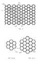
- FIGS. 5 a - 5 bare schematic diagrams showing a cylindrical micromirror array lens including hexagonal micromirrors, and a circular micromirror array lens including hexagonal mirrors, respectively, according to one embodiment of the present invention
- FIG. 6is a schematic diagram showing a cylindrical micromirror array lens including rectangular micromirrors, according to one embodiment of the present invention.
- FIG. 7is a schematic diagram showing a circular micromirror array lens including triangular micromirrors, according to one embodiment of the present invention.
- FIGS. 8( a )- 8 ( b )are schematic views of a beam focusing and scanning system using a micromirror array lens, according to two embodiments of the invention.
- FIGS. 8( c )- 8 ( d )are flow diagrams of methods in a beam focusing and scanning system using a micromirror array lens, according to various embodiments of the invention.
- FIG. 9is a partial top view of a lens array, according to one embodiment of the present invention.
- FIGS. 10( a )- 10 ( b )are top views of micromirror array lenses included in the lens array of FIG. 9 , according to one embodiment of the present invention.
- FIG. 11is a top view of a lens array including a micromirror array lens at a first point in time, according to one embodiment of the present invention.
- FIG. 12is a top view of a lens array including a micromirror array lens at another point in time, according to one embodiment of the present invention.
- FIG. 13is a schematic side view of a micromirror array lens, according to one embodiment of the present invention.
- FIG. 14is a schematic view illustrating operation of a two-dimensional projection device, according to one embodiment of the present invention.
- FIG. 15is a block diagram showing a random scanning technique in a two-dimensional image projection device, according to one embodiment of the present invention.
- FIG. 16is block diagram showing a self diagnosis and correction process in a two-dimensional image projection device, according to one embodiment of the present invention.
- FIG. 17is a schematic diagram showing a portable electronic device including a lens array, according to one embodiment of the present invention.
- FIG. 18is a schematic view of an optical pick-up device in accordance, according to one embodiment of the present invention.
- FIGS. 19( a )- 19 ( b )are schematic side views illustrating an analogy between a concave mirror and a micromirror array lens (Frensel reflective lens), according to one embodiment of the present invention
- FIGS. 20( a )- 20 ( b )are schematic side views illustrating an example of the operation of a micromirror array lens to perform phase compensation in compensating for the tilt of an optical disc, according to one embodiment of the present invention
- FIG. 21is a schematic side view illustrating operation of a micromirror array lens to record data on or read data from a multi-layered optical disk, according to one embodiment of the present invention.
- FIG. 22a schematic top view of an micromirror array including multiple micromirror array lenses, according to one embodiment of the present invention.
- FIG. 23is a schematic side view of a portion of an optical pick-up device including a lens array having multiple micromirror array lenses, according to one embodiment of the present invention.
- FIG. 24is a schematic side view of a high-speed optical pick-up device including a lens array having multiple micromirror array lenses, according to one embodiment of the present invention.
- micromirror array lensincludes micromirrors and actuating components, and uses a simpler mechanism to control focusing system than in prior art approaches.
- the focal lengthis varied by displacement of each micromirror.
- FIG. 1illustrates the principle of the micromirror array lens 111 .
- two conditionsmust be satisfied. First, light scattered by one point of an object should converge into one point on the image plane. Second, converging light should have the same phase at the image plane. To satisfy these conditions, the surface shape of a conventional reflective lens 112 is formed to have all lights scattered by one point of an objective to converge into one point on the image plane and have the optical path length of all converging light to be same.
- a micromirror array arranged in flat planecan also satisfy these two conditions.
- Each of the micromirrors 113rotates to converge the scattered light.
- all micromirrors 113 of the micromirror array lens 111are arranged in a flat plane as shown in FIG. 1 , the optical path length of lights converged by rotation of the micromirrors is different. Even though the optical path length of converging light is different, the same phase condition can be satisfied by adjusting the phase because the phase of light is periodic.
- FIG. 2illustrates the in-plane view of the micromirror array lens 221 .
- the micromirror 222has the same function as a mirror. Therefore, the reflective surface of the micromirror 222 is made of metal, metal compound, multi-layered dielectric material, or other materials with high reflectivity. Many known microfabrication processes can make the surface with high reflectivity.
- Each micromirror 222is electrostatically and/or electromagnetically controlled by the actuating components 223 as known.
- the micromirror array lens 221has a polar array of the micromirrors 222 .
- Each of the micromirrors 222has a fan shape to increase an effective reflective area, which increases optical efficiency.
- micromirrorsare arranged to form one or more concentric circles to form the axisymmetric lens and the micromirrors on the same concentric circle can be controlled by the same electrodes or independently controlled by known semiconductor microelectronics technologies such as MOS or CMOS.
- each reflective micromirror 222 and the actuating components 223are located under the micromirrors 222 to increase the effective reflective area.
- electric circuits to operate the micromirrorscan be replaced with known semiconductor microelectronics technologies such as MOS and CMOS. Applying the microelectronics circuits under micromirror array, the effective reflective area can be increased by removing necessary area for electrode pads and wires used to supply actuating power.
- FIG. 3illustrates how the micromirror array lens 331 images.
- Arbitrary scattered lights 332 , 333are converged into one point P of the image plane by controlling the positions of the micromirrors 334 .
- the phases of arbitrary light 332 , 333can be adjusted to be same by translating the micromirrors 34 .
- the required translational displacementis at least half of the wavelength of light.
- each of the micromirrors 334has a curvature because the ideal shape of a conventional reflective lens 112 has a curvature. If the size of the flat micromirror is small enough, the aberration of the lens comprising flat micromirrors 334 is also small enough. In this case, the micromirror does not need a curvature.
- the focal length f of the micromirror array lens 331is changed by controlling the rotation and the translation of each micromirror 334 .
- FIG. 4shows two degree of freedom rotations and one degree of freedom translation of the micromirror 441 .
- the arraycomprising micromirrors 441 with two degree of freedom rotations 442 , 443 and one degree of freedom translation 444 , which are controlled independently can make a lens with arbitrary shape and/or size.
- Incident lightscan be modulated arbitrarily by forming an arbitrary shape and/or size lens. To do this, it is required that incident lights are deflected to an arbitrary direction by controls of two degree of freedom rotations 442 , 443 .
- Independent translation 444 of each micromirroris also required to satisfy the phase condition.
- FIGS. 5 a, 5 b, 6 and 7the rotational amount of a micromirror is represented by length of arrow 552 and the profile gradient direction to represent a rotational direction of a micromirror is represented by direction of arrow 552 .
- FIG. 5 ashows a variable focal length cylindrical lens comprising hexagonal micromirrors 551 .
- FIG. 5 bshows a variable focal length circular lens 553 comprising hexagonal micromirrors 551 . Shape, position and size of the variable focal length circular lens 553 can be changed by independent control of micromirrors 551 with two DOF rotations and one DOF translation.
- micromirrors 555which are not elements of the lens are controlled to make lights reflected by the micromirrors 555 not have influence on imaging or focusing.
- FIGS. 5 a - 5 bshow hexagonal micromirrors 551 , fan shape, rectangle, square, and triangle micromirrors array can be used.
- An array comprising fan shape micromirrorsis appropriate to an axisymmetric lens.
- FIG. 6shows a variable focal length cylindrical lens 661 comprising rectangular micromirrors 662 .
- An array comprising square or rectangle micromirrors 662is appropriate to a symmetric lens about one in-plane axis such as cylindrical lens 661 .
- the micromirrors with same rotationare controlled by the same electrode or controlled by known semiconductor microelectronics technologies such as MOS or CMOS independently.
- FIG. 7shows a variable focal length circular lens 771 comprising triangular micromirrors 772 .
- An array comprising triangular micromirrors 772is appropriate to a lens with arbitrary shape and/or size lens like an array comprising hexagonal micromirrors.
- the micromirror array lensis an adaptive optical component because the phase of light can be changed by controlling the translations 444 and rotations 442 , 443 of micromirrors independently, referring again to FIG. 4 .
- adaptive optical micromirror array lensrequires two-dimensional arrays of individually addressable micromirrors. To achieve this, it is necessary to combine the micromirrors with on-chip electronics. In order to do this, wafer-level integration of micromirrors with the known microelectronics circuits is necessary.
- the micromirror array lenscan correct the phase errors since an adaptive optical component can correct the phase errors of light due to the medium between the object and its image, and/or correct the defects of a lens system that cause its image to deviate from the rules of paraxial imagery.
- the micromirror array lenscan correct the phase error due to optical tilt by adjusting the translations 444 and rotations 442 , 443 of micromirrors.
- the same phase condition satisfied by the micromirror array lenscontains an assumption of monochromatic light. Therefore, to get a color image, the micromirror array lens is controlled to satisfy the same phase condition for each wavelength of Red, Green, and Blue (RGB), respectively, and the imaging system can use bandpass filters to make monochromatic lights with wavelengths of Red, Green, and Blue (RGB).
- RGBRed, Green, and Blue
- a color imagecan be obtained by processing electrical signals from Red, Green, and Blue (RGB) imaging sensors with or without bandpass filters, which should be synchronized with the control of micromirror array lens.
- RGBRed, Green, and Blue
- the micromirror array lensis controlled to satisfy the phase condition for Red light.
- Red, Green, and Blue imaging sensorsmeasure the intensity of each Red, Green, and Blue light scattered from an object. Among them, only the intensity of Red light is stored as image data because only Red light is imaged properly.
- the micromirror array lens and each imaging sensorworks in the same manner as the process for the Red light.
- the micromirror array lensis synchronized with Red, Green, and Blue imaging sensors.
- the same phase condition for a color imageis satisfied by using the least common multiple of wavelengths of Red, Green, and Blue lights as an effective wavelength for the phase condition.
- the micromirror array lensis not necessary to be controlled to satisfy the phase condition for each Red, Green, and Blue light individually. Instead, the phase condition for the least common multiple of the wavelengths should be satisfied.
- each micromirroris only controlled to satisfy the phase condition for one light among Red, Green, and Blue lights or is not controlled to satisfy the phase condition for any other lights of Red, Green, and Blue.
- the micromirror array lenscannot satisfy the phase condition due to phase error of lights with multi-wavelength, still the lens can be used as a variable focal length lens with low quality.
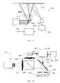
- FIGS. 8( a )- 8 ( b )are schematic views of a beam focusing and scanning system using a micromirror array lens (optical system).
- an optical system 820includes a light source 822 configured to emit light 821 .
- the optical system 820also includes a micromirror array lens 830 , including at least one micromirror (see element 222 in FIG. 2) , optically coupled to the light source 822 , configured to focus the light onto a projection medium 825 (projection plane).
- the projection medium 825may be, for example, paper, a television screen, a movie screen, or any other type of projection medium.
- the projection medium 825is optically coupled to the micromirror array lens 830 , and is configured to receive the light focused by the micromirror array lens 830 .
- the optical system 820also includes at least one actuating component (see element 223 in FIG. 2 ) coupled to the at least one micromirror of the micromirror array lens 830 , configured to move the at least one micromirror to enable the at least one micromirror to focus the light on the projection medium 825 .
- movement of the at least one micromirror by the at least one actuating componentincludes translation in one degree of freedom and rotation in two degrees of freedom, as described further with reference to FIG. 4 .
- movement of the at least one micromirror by the at least one actuating componentis configured to scan the projection medium by traversing the light focused by the micromirror array lens across the projection medium 825 .
- the scan of the projection medium 825may be configured to allow data to be recorded to the projection medium 825 .
- movement of the at least one micromirror by the at least one actuating componentis configured to compensate for light phase aberrations, as described further with reference to FIGS. 20( a )- 20 ( b ).
- the optical system 820also includes a control circuitry coupled to the at least one actuating component, configured to control movement of the at least one micromirror by the at least one actuating component.
- the control circuitrymay include, for example, semiconductor microelectronics. (refer to FIG. 2 )
- movement of the at least one micromirror by the at least one actuating componentis controlled by electrostatic force, electromagnetic force, or a combination of electrostatic and electromagnetic forces (refer to FIG. 2 ).
- the optical system 840also includes a beam splitter 826 (refer to 1826 in FIG. 18) , optically coupled to the light source 822 configured to split the light rays 821 .
- the light source 822emits light that passes through a first optical lens 824 (refer to 1824 in FIG. 18 ).
- the first optical lenscreates a collimated light beam which is passed to the beam splitter 1826 .
- a second optical lens 828(refer to 1828 in FIG. 18 ) receives portion of the light rays 821 from the beam splitter 826 and focuses the light rays onto a read sensor 875 .
- the read sensor 875is optically coupled to the micromirror array lens 830 and is configured to read data from the projection medium 825 in response to a scan of the projection medium by traversing the light focused by the micromirror array lens 830 across the projection medium 825 .
- movement of the at least one micromirror by the at least one actuating componentmay be configured to compensate for light phase aberrations, as described further with reference to FIGS. 20( a )- 20 ( b ).
- FIG. 8( c )is a flow diagram of a method in a beam focusing and scanning system using a micromirror array lens.
- step 880light is emitted from a light source onto a micromirror.
- step 885the position of the micromirror is adjusted to focus the light onto a projection medium.
- FIG. 8( d )is a flow diagram of a method in a beam focusing and scanning system using a micromirror array lens.
- step 890light is emitted from a light source onto a micromirror.
- step 895the position of the micromirror is adjusted to focus and scan the light onto a projection medium.
- the methodalso includes adjusting the position of the micromirror to compensate for light phase aberrations.
- the methodalso includes scanning the projection medium by traversing the light focused by the micromirror array lens across the projection medium.
- the methodalso includes recording data to the projection medium in response to the scanning of the projection medium.
- the methodalso includes sensing light reflected from the projection medium in response to the light focused by the micromirror array lens and reading data from the projection medium in response to the sensing of the light reflected from the projection medium.
- Possible applications of the beam focusing and scanning system described with reference to FIGS. 8( a )- 8 ( c )are two-dimensional image projection devices, printers, optical pick-ups, and scanners. These applications are exemplary only. Other applications are also possible.
- a two-dimensional image projection devicecomprising an array of micromirror array lenses.
- Each micromirror array lenscomprises a plurality of micromirrors, whose configurations may be adjusted to change the focal length, optical axis, lens size, the number of lenses, shape of lens, and others of the micromirror array lens.
- the array of micromirror array lensesgreatly improve the brightness of the projected image and the power consumption of the display device by increasing light efficiency.
- the optical system 820may be applied in a two-dimensional image projection device comprising a light source 822 , a lens array 830 , and a projection plane 825 .
- the light source 822may be any conventional light source, such as a metal halide with a color wheel, a light emitted diode, a three (Red, Green, Blue) laser diode, or any other suitable light source.
- the light sourcegenerates Red, Green, and Blue (“RGB”) light 821 , which is reflected by the lens array 830 according to the image data, and focused onto the projection plane 825 , where the resulting image is displayed.
- RGBRed, Green, and Blue
- the lens array 830comprises a planar array of micromirror array lenses 932 , 934 , and 936 .
- Each micromirror array lenscomprises a plurality of micromirrors 938 .
- the micromirrors 938have the same function as a mirror and comprise a reflective surface made of metal, metal compound, or other materials with reflectivity. Many known microfabrication processes can be used to fabricate a surface having high reflectivity.
- the micromirrorsare individually controlled by actuating components that rotate and translate the micromirrors.
- the micromirrorsare preferably parabolic in cross-section. This parabolic construction increases the focusing efficiency of the micromirror array lens, as discussed in further detail below.
- the lens array 830may comprise a series of micromirror array lenses 932 , 934 , and 936 arranged to form a substantially rectangular array.
- the basic configuration and operational principle of such a lens arrayis described in and U.S. patent application Ser. No. 10/857,714 (filed May, 28, 2004), the entire disclosure of which is incorporated herein by reference.
- each micromirror array lenscomprise an arbitrary number of micromirrors 938 that may vary in size and shape. However, it is preferred that the micromirrors comprise a hexagonal, rectangular, and/or square shape. These shapes enable the micromirrors to be easily fabricated and controlled.
- a cylindrical lens array or mixed lens arraycomprising cylindrical and/or circular lenses may be constructed.
- the relative positions of the micromirror array lens 932 , 934 , and 936are not fixed in the plane of the lens array 830 .
- Each micromirror array lensexists for a given time.
- many different micromirror array lensesare “constructed” and “destroyed” within the frame speed.
- one image framemay only require that the lens array 830 comprise only one micromirror array lens 932 , as shown in FIG. 11 .
- another image framemay require that the lens array comprise twelve micromirror array lenses 932 , as shown in FIG. 12 .
- the word “variable”means all optical parameters, focal length, optical axis, lens size, the number of lenses, shape of lens, and others are changed according to the processed image data.
- micromirror array lensso long as each micromirror has corresponding slant and the micromirrors are configured such that phases of the converging light are the same.
- FIG. 13illustrates how each micromirror array lens 932 , 934 , and 936 works.
- the micromirror array lens of the present inventionis very similar to the prior art micromirror array lens proposed by J. Boyd and G. Cho in their paper entitled, “Fast-response Variable Focusing Micromirror Array Lens”, Proc. SPIE, Vol. 5055, 278-286 (2003), the disclosure of which is hereby incorporated by reference as if set forth in full herein.
- the micromirror array lens 932comprises many micromirrors 938 .
- Each micromirrorcorresponds to a segment of a circle or a parabola.
- the micromirror array lenscan change its focal length and direction of optical axis by controlling the slant of each segmental micromirror.
- the micromirror array lens 932produces an in-focus image pixel by converging collimated light 1337 into one point M (see FIG. 8 ) on an image plane. This is accomplished by controlling the position of the micromirrors 938 .
- the phases of the arbitrary lightmay be adjusted to the same phase by translating each one of the micromirrors.
- the required translational displacement range of the micromirrorsis at least half of the wavelength of light.
- the focal length F of the micromirror array lens 932is changed by controlling the rotational and/or translational motion of each micromirror 938 .
- the micromirror array lenscan be a Spatial Light Modulator (SLM).
- SLMSpatial Light Modulator
- the micromirrorsretract or elevate to length or shorten the optical path length of light scattered from the image, to remove phase aberrations from the image.
- the mechanical structures upholding the micromirrors 938 and the actuating components that rotate and translate the micromirrorsare located under the micromirrors to enable the micromirrors to be positioned closer to one another. This increases the effective reflective area of the micromirror array lens 932 .
- electric circuits to operate the micromirrorscan be replaced with known microelectronic technologies, such as MOS or CMOS. Applying the circuits under the micromirror array, the effective area can be increased by removing necessary area for the electrode pads and wires used to supply actuating power. Since the micromirrors are small in mass and have small moments of inertia, their positions and attitudes may be changed at rate of approximately 10 kHz. Therefore, the micromirror array lens becomes a high speed variable focusing lens having a focusing response speed of approximately 10 kHz.
- each micromirror 938have a curvature because the ideal shape of a conventional reflective lens has a curvature.
- the aberration of the micromirror array lens 932 with flat micromirrorsis not much different from a conventional lens with curvature if the size of the micromirrors is small enough, there is not much need to control the curvature of the micromirrors.
- the present inventionprovides each micromirror 938 with three degrees-of-freedom motion, one translational motion 444 along the normal axis to the plane of each micromirror array lens, and two rotational motions 442 , 443 about two axes in the plane of each micromirror array lens.
- the translational motionis required to meet phase matching condition to compensate for aberrations.
- the two rotational motionsare required to deflect light arbitrary direction and are essential for versatility of the array of micromirror array lenses.
- An array of micromirror array lenses with only two-degree-of-freedom rotational motionis also possible but its image quality may be deteriorated.
- FIG. 14illustrates the operation of a two-dimensional image projection device 1450 , such as a beam projector or a projection television, comprising a lens array 1454 in accordance with principles of the present invention.
- a light source(not shown) generates collimated light 1451 that incidents from the light source to the lens array 1452 .
- the lightis reflected from the micromirror array lenses 1456 and focused onto a projection plane 1460 , wherein the resulting image is viewed.
- the center or optical axis of a micromirror array lensmay vary.
- the number of micromirrors comprising a micromirror array lens, or the focal length of a micromirror array lensmay vary. Since each micromirror array lens has the ability to scan the in-focused light along the projection plane, any two or more micromirror array lenses can simultaneously focus incident light onto different positions, or the same position along the projection plane. Because each micromirror array lens can scan the whole plane 1460 (i.e., focus the incident light at any position along the plane), the projected image can be generated.
- Two-dimensional image projection devices of the present inventionmay apply a random scanning technique (“RST”) to reduce the required number of micromirror array lenses comprising a lens array.
- FIG. 15schematically illustrates how the RST is applied to such image projection devices.
- the techniquebegins with an image signal 1510 that is received from an antenna and/or receiving means.
- the signalis then processed by an image processor that analyses the average brightness of a frame 1520 .
- the image processorthen analyses brightness of each pixels 1530 .
- the image processorcalculates the required light intensity and exposure time 1540 for each pixel.
- the image processorthen performs optimization 1550 .
- the most optimized set of micromirror array lens combinationswhich can minimize the movement, minimize construction and destruction of the micromirror array lens, and the minimize scanning length for a frame rate is generated.
- a control command for a frameis generated 1560 .
- the control signalis sent to lens array to generate images on the screen.
- a two-dimensional image projection system using array of micromirror array lenses and the random scanning techniquecan display much more pixels than the number of micromirror array lenses.
- the gray scalecan be expressed easily.
- the fact that the required number of micromirror array lens is much smaller than the number of pixelsmakes the array of micromirror array lenses very small in size.
- the display devicecan express fine images if the array of micromirrors comprise enough micromirrors.
- a self diagnosis & correction techniquemay also be applied to a two-dimensional image projection device.
- the image processoranalyzes the deviations of each spot from a predetermined position and correct the scale factor of the corresponding micromirror.
- FIG. 16A simplified schematic diagram of the SDCT as applied to a two-dimensional image projection device of the present invention is shown in FIG. 16 .
- the SDCT systemmainly consists of a light source 1610 , an image sensor 1650 , an image processor 1660 , read only memory (ROM) 1670 , a lens array 1620 , and controller 1640 .
- the controller 1640generates and sends a set of test signals to the lens array 1620 .
- Each of the micromirrors comprising the arrayis controlled by the test signal, and incident light from the light source 1610 is deflected to several predetermined positions 1635 along a projection plane 1630 by the controlled micromirrors.
- the image sensor 1650comprises a photo detector that detects the light spots along the projection plane.
- the image sensorthen sends an electrical signal comprising image data to the image processor 1660 .
- the image processoralso decides the pass or failure of each micromirror. This test will be done for all micromirrors in the lens array.
- the response speed of the micromirrorsare slightly less than 10 kHz, entire the test can be completed for all micromirrors within a few minutes. The test also can be done while viewers are watching the image device. The test results for all micromirrors in the array is written in the ROM 1670 and become reference data for the random signal processing. In the random scanning processing for two-dimensional image displaying, the failed micromirrors are excluded in construction of micromirror array lenses.
- the random signal processoroptimizes the control signals to exclude failed micromirrors in operation and to compensate by adjusting the micromirror array lens combination and scanning speed.
- the SDCTthe displayed image can be maintained with the same quality even if as many as ten to twenty percent (10 ⁇ 20%) of micromirrors are failed.
- the reliability and operating lifetime of display devicecan be much improved.
- the DMD arrayuses at most fifty percent (50%) of incident light because it has “on” and “off” positions. The light is dumped when the mirror is at “off” position.
- the array of micromirror array lensescan use most incident light by adopting the optimized Random Scanning Technique, discussed above.
- the most power consuming element in a two-dimensional display deviceis projection lamp, and light efficiency is directly related to power consumption.
- micromirror array lensesis incorporated into small electronic devices such as mobile phones, PDAs, camcorders, and other related devices.
- the micromirror array lensesmay be small in construction, which enables the array to be used with such devices.
- FIG. 17illustrates an example of a two-dimensional image projector of the present invention implemented within a small portable electronic device.
- a three (Red, Green, Blue) laser diode module 1710is used as a light source.
- a broad band laseris preferable.
- An image signal 1760 received from a broadcasting system, other outside device, or internal storage deviceis transmitted to a random scanning processing unit 1770 , which sends an optimized control signal to construct a lens array 1720 .
- the lens arraydeflects incident light from the laser diode to display an image.
- the imagecan be displayed on a screen, wall, or other suitable projection plane 1730 .
- An image sensor 1740 implemented into the portable electronic devicecomprises a photo detector that detects scattered light from the screen.
- the image sensorgenerates and sends to an automatic focusing image processor 1750 an electrical signal carrying image data.
- the image processorcontains an automatic focusing algorithm that analyzes the image data to determine the focusing status.
- the image processorthen sends the focusing status to a random scanning processing unit 1770 .
- Random scanning processing unitsends a control signal to the micromirror array lenses to adjust the focusing of each of the micromirror lenses in the lens array.
- the present inventionimproves the brightness and power consumption of conventional two-dimensional image projection systems.
- the present inventionmay be adapted to provide portable, pocked-sized, high quality two-dimensional image projection devices.
- Each of the micromirror array lenses comprising the lens array of the present inventionmay be controlled independently to have different focal lengths, different optical axes, lens sizes, and lens shapes. This enables the lens array to be applied in many applications. Further, each of the micromirror array lenses of the lens array may be controlled to scan a plane with different speeds, or a group of micromirror array lenses may be controlled to scan the same point on a plane simultaneously. This makes easy to control the light intensity on the screen.
- an optical pick-up devicefor use in an optical recording/reproducing system.
- the optical pick-up devicecomprises at least one variable focal length micromirror array lens.
- the micromirror array lensrecords and/or reads information on or from an optical disc.
- the present inventionprovides focusing, tracking, and tilt compensation of the optical pick-up with minimal macroscopic motion.
- the optical pick-up device 1820includes a laser diode 1822 , a first optical lens 1824 , a beam splitter 1826 , a second optical lens 1828 , a micromirror array lens 1830 , a sensor 1840 , a tilt detector 1851 and a signal processor 1850 .
- the foregoing componentsare preferable packaged as a single unit within the device. However, various components of the device, such as the signal processor, may be remote or detachable from the device.
- the first and second optical lenses 1824 and 1828are preferably conventional refractive lenses having fixed focal lengths. As illustrated in FIG. 18 , the laser diode 1822 emits a laser beam that passes through the first optical lens 1824 . The first optical lens created a collimated light beam which is passed to the beam splitter 1826 . The collimated beam passed to the beam splitter 1826 is then focused onto a signal recording surface of an optical disc 1860 by the micromirror array lens 1830 . The optical disc reflects a portion of the light beam back towards the micromirror array lens. The reflected light is collimated by the micromirror array lens and deflected substantially 90°, towards the beam splitter. The beam splitter deflects the reflected light substantially 90°, towards the second optical lens 1828 . The second optical lens focuses the reflected beam on the sensor 1840 .
- the micromirror array lens 1830is a variable focal length lens.
- Such a micromirror array lenswas proposed by James G. Boyd IV and Gyoungil Cho in their paper entitled, “Fast-response Variable Focusing Micromirror Array Lens”, Proc. SPIE , Vol. 5055, pp. 278-286 (2003), and improvements of the micromirror array lens are disclosed in U.S. patent application Ser. No. 10/806,299 (filed Mar. 23, 2004), Ser. No. 10/855,554 (filed May 27, 2004), Ser. No. 10/855,715 (filed May 27, 2004), Ser.
- the micromirror array lens 1830preferably comprises a plurality of micromirrors 222 concentrically arranged in a plane to form one or more concentric circles.
- the micromirrors 222have the same function as a mirror and comprise a reflective surface made of metal, metal compound, or other materials with high reflectivity. Many known microfabrication processes may be used to make the surface have high reflectivity.
- the micromirrorspreferably comprise a parabolic cross-section and have a fan shape. This fan-shaped construction with curvature increase the effective reflective area and focusing efficiency of the micromirror array lens.
- the reflective surface of the micromirrorsmay be flat.
- the micromirrors 222are individually controlled electrostatically and/or electromagnetically by actuating components that rotate and translate the micromirrors.
- the micromirrorsare controlled to change the focal length of a micromirror array lens 1830 by controlling their translational and/or rotational motions.
- the mechanical structures upholding the micromirrors 222 and the actuating components that rotate and translate the micromirrorsare located under the micromirrors to enable the micromirrors to be positioned closer to one another. The close positioning of the micromirrors increases the effective reflective area of the micromirror array lens.
- each micromirror 222has three degrees-of-freedom motion, one translational motion 444 along the normal axis to the plane of each micromirror array lens, and two rotational motions 442 and 443 about two axes in the plane of each micromirror array lens.
- the translational motionis required to meet phase matching condition to compensate for aberrations.
- the two rotational motionsare required to deflect light arbitrary direction and are essential for versatility of the array of micromirror array lenses.
- FIGS. 19( a )- 19 ( b )illustrate the principle of a micromirror array lens and the analogy between a micromirror array lens 1830 and a conventional concave mirror 1935 .
- a concave mirrorfunctions as a convex refractive lens.
- the micromirror array lensis effectively a type of reflective Frensel lens.
- a micromirror array lenscomprises a plurality of micromirrors 222 .
- the micromirror array lenscan change its focal length by controlling the rotational and/or translational motion of micromirrors.
- the micromirror array lensconverges arbitrarily scattered light 1934 onto a focal point F by controlling the positions of the micromirrors 222 (see FIG. 2 ).
- the phases of the arbitrary lightmay be adjusted to be the same by translating each one of the micromirrors.
- the required translational displacement range of the micromirrorsis at least half of the wavelength of light.
- the focal length of the micromirror array lens 1830is changed by controlling the rotational and/or translational motion of each micromirror.
- the lenscan correct defect and aberration which are caused by various optical effects such as optical tilt, mechanical deflection, and so on.
- the micromirrorscan correct the phase error of light scattered from the disc to remove phase aberration by controlling the amounts of their translations.
- the lensalso has a high optical focusing efficiency and can have a large size aperture without losing optical performance.
- the lenshas low production cost because of the advantages of its mass productivity typical of microfabrication methods.
- the lenscan also make the focusing system much simpler due to its simple structure.
- the senor 1840comprises a photo detector.
- the photo detectorconverts photon energy of the light reflected by the optical storage media 1860 into electric signal, in the form of an electrical data signal 1845 .
- the senorthen sends the generated data signal to the signal processor 1850 for processing.
- the sensormay be a coupled charge device (CCD), a CMOS image sensor, or any other suitable alternative.
- the senormay comprise one or more photo detectors for detecting focus error and tracking error signals.
- the signal processor 1850is preferably a processing unit comprised within or detachable from the optical pick-up device 1820 .
- the signal processoruses an algorithm to analyze the data signal from the sensor 1840 .
- One of various well-known conventional signal processing algorithmscan be used depending on the application.
- the tilt detector 1851measures the tilt of the optical disc. The measured tilt is sent to the signal processor 1850 .
- the signal processorprocesses the data signal received from the senor and the tilt detector and generates a reproduction or RF signal 1853 corresponding the recorded information on the optical disc, and controls signals 1855 which are sent to micromirror array lens to compensate for correct tracking error, focusing error, and tilt error.
- FIGS. 20( a )- 20 ( b )are schematic side views illustrating an example of the operation of a micromirror array lens to perform phase compensation in compensating for the tilt of an optical disc. It shall be understood that the movement of the micromirrors can compensate for differences in phase for any device application and compensating for tilt and deflection of the optical disc 1860 is only one example. Phase compensation may be performed for any focusing or scanning operation.
- the micromirror array lens 1830maintains the focus at the point P on the disc by changing its focal length and optical axis.
- the micromirror array lens 1830can also correct various aberrations because the lens is an adaptive optical lens.
- the lenscan compensate for a focusing error, a tracking error, and aberration by tilt and/or mechanical deflection.
- FIG. 18illustrates how optical pick-up devices of the present invention reads data from an optical disc 1860 .
- the laser diode 1822emits a laser beam which is passed through the first optical lens 1824 .
- the first optical lenscollimates the light beam.
- the light beamis then passed to the beam splitter 1826 .
- the lightis passed from the beam splitter to the micromirror array lens 1830 .
- the micromirror array lensdeflect the light beam substantially 90°, and focuses the light on a tracking location on a data layer of the optical disc 1860 .
- Light reflected from a reflective layer of the optical discis collimated by the micromirror array-lens 1830 , and deflected back towards the beam splitter 1826 .
- the beam splitterthen deflects the reflected light substantially 90°, towards the second optical lens 1828 .
- the second optical lenspasses the reflected light and focuses it on the sensor 1840 .
- the sensordetects the intensity of the reflected light from the reflective layer of the optical disc, and generates an electrical signal 1845 based on the intensity of light it receives.
- the reflected lightis more diffused, or has a weak intensity when it hits a pit 1863 in the data layer.
- the reflected lighthas a strong intensity when it strikes the smooth areas, or lands 1865 , in between the pits.
- the data signalis generated by pits and lands.
- the electrical signalis passed to the signal processor 1850 .
- the signal processorgenerates a reproduction signal 1853 .
- the signal processoralso generates control data 1855 which is sent to the micromirror array lens to adjust the micromirrors to compensate for tracking error, focusing error, and tilt error.
- optical pick-up devices of the present inventionare capable of writing data onto the optical disc 1860 .
- the intensity of the laser beam emitted by the laser diode 1822is varied according to a data signal transmitted to the laser diode via a data storage device (not shown) within the optical recording/reproducing system.
- the laser beamis passed through the first optical lens 1824 .
- the first optical lenscollimates the light beam.
- the light beamis then passed to the beam splitter 1826 .
- the lightis passed from the beam splitter to the micromirror array lens 1830 .
- the micromirror array lensdeflect the light beam substantially 90°, and focuses the light on the dye layer of the optical disc 1860 .
- the dye used to form the optical discreacts to the heat and light to create a series of recorded pits and lands corresponding the stored data.
- the optical pick-up devicemay comprise a tilt detector 1851 , as shown in FIG. 18 .
- the tile detectordetects the tilt of the optical disc and generates a tilt signal 1852 in response to the detected tilt.
- the tilt signalis transmitted to the signal processor 1850 .
- the signal processorprocesses the tilt signal and transmits a control signal 1855 to the micromirror array lens to compensate for tilt error.
- a magnetically driven conventional lenshas both focusing and tracking motions to record information on a disc or to read the recorded information from the disc.
- a conventional lensis moved macroscopically in one or more directions to compensate for the optical tilt, which results in comma aberration.
- the micromirror array lens 1830can cover the focusing, tracking, and tilt compensation operations of a conventional lens without macroscopic motions. This possible because the micromirror array lens is a variable focal length lens, capable of changing optical axis and compensating for aberrations by the microscopic three-degree-of-freedom motions of each micromirror.
- micromirror array lenses 1830 of the present inventionare capable of recording data on and reading data from a multi-layered optical disc 2170 .
- the micromirror array lensrecords and/or reads information at each layer of a multi-layered optical disk by changing its focal length to focus on the desired layer.
- the optical pick-up devicemay comprise a planar array 2230 of micromirror array lenses 2232 , 2233 , 2234 with different shapes, sizes, and numbers of micromirrors 2236 .
- a planar array 2230 of micromirror array lenses 2232 , 2233 , 2234 with different shapes, sizes, and numbers of micromirrors 2236is disclosed in U.S. patent application Ser. No. 10/857,714 (filed May 28, 2004), the disclosure of which is hereby incorporated by reference as if set forth in full herein.
- each micromirror array lensis not fixed in the plane and many different micromirror array lenses 2232 , 2233 , 2234 can be “created” and “deleted”.
- the total number of lenses comprising the arrayis variable according to the purpose of the array.
- the micromirror array lensesare not limited to the configuration shown in FIG. 22 .
- the micromirrorscan have arbitrary shapes and sizes, and form a lens with arbitrary shape and size or an array of micromirror array lenses. Even though only the hexagonal shape is shown in FIG. 22 , the micromirrors can have different shapes to form different types of lens arrays without losing their effective reflective area.
- the control circuitry of the lenscan be constructed by known microelectronics technology which is located under the mirrors.
- each micromirror array lens 2232can have a different optical axis, different number of micromirrors 2236 , and different focal length. Since each micromirror array lens 2232 also can freely change its optical axis and focal length with three-degree-of-freedom motions of its micromirrors, each micromirror array lens causes incident light 2340 to focus at any position in a plane 2350 or scan the whole plane.
- FIG. 24shows a high-speed optical pick-up device of the present invention with a planar array 2230 of micromirror array lenses 2232 .
- the micromirror array lenscan cover the focusing, tracking, and/or tilt compensation operational motions of a conventional optical pick-up device.
- macroscopic motionis only needed for the tracking operation of the device using the micromirror array lens.
- the array 2230is set to cover the whole radial region of a disc 2460 , even the tracking operation will be covered and then there will be no macroscopic motions in the optical pick-up device.
- each lens of the lens arraycan change its focal length and optical axis very fast by controlling each of their micromirrors 2234 , each lens is only required to scan its assigned region of the disc without any macroscopic motion and is much faster than a micromirror array lens with tracking operations.
- the systemcan be sped up as more lenses 2232 are added to the array in the radial direction.
- the optical recording/reproducing systemcan improve its reliability and reading/writing speed with high optical focusing efficiency by removing moving parts in the optical pick-up device.
- optical information recording mediathere exist many kinds of optical information recording media, and the standards of these optical information recording media are established. Because the optical information recording media have different recording densities, interchangeability between CD and DVD is required. These optical information recording media have different thicknesses of the transparent base board. In order to obtain the interchangeability, it is necessary to correct a spherical aberration generated by the difference of the thickness of the transparent base boards. The spherical aberration can be compensated by controlling the rotations and/or translations of micromirrors.
- a lens arrayis an array of lenses.
- a micromirror arrayis an array of micromirrors.
- a micromirror array lensis a lens composed of an array of micromirrors.
- a micromirror array lensis composed of at least one micromirror. Operation of at least one micromirror may be considered operation of a micromirror array lens.
- each micromirrormay be moved independently by its respective actuating component.
- the advantages of the present inventioninclude high speed variable focusing and scanning, large focal length variation, phase compensation, high reliability and optical efficiency, low power consumption and low cost.
Landscapes
- Physics & Mathematics (AREA)
- General Physics & Mathematics (AREA)
- Optics & Photonics (AREA)
- Electromagnetism (AREA)
- Nonlinear Science (AREA)
- Mechanical Light Control Or Optical Switches (AREA)
- Facsimile Scanning Arrangements (AREA)
- Optical Head (AREA)
Abstract
Description
Claims (16)
Priority Applications (5)
| Application Number | Priority Date | Filing Date | Title |
|---|---|---|---|
| US10/979,568US7354167B2 (en) | 2004-05-27 | 2004-11-02 | Beam focusing and scanning system using micromirror array lens |
| KR1020077012636AKR20070085760A (en) | 2004-11-02 | 2005-11-02 | Beam Focusing and Scanning System Using Micromirror Array Lenses |
| PCT/US2005/039655WO2006050431A2 (en) | 2004-11-02 | 2005-11-02 | Beam focusing and scanning system using micromirror array lens |
| TW094138500ATWI266893B (en) | 2004-11-02 | 2005-11-02 | Beam focusing and scanning system using micromirror array lens |
| US11/341,030US7667896B2 (en) | 2004-05-27 | 2006-01-28 | DVD recording and reproducing system |
Applications Claiming Priority (11)
| Application Number | Priority Date | Filing Date | Title |
|---|---|---|---|
| US10/855,287US6934072B1 (en) | 2004-05-27 | 2004-05-27 | Variable focal length lens comprising micromirrors with two degrees of freedom rotation and one degree of freedom translation |
| US10/855,554US6970284B1 (en) | 2004-05-27 | 2004-05-27 | Variable focusing lens comprising micromirrors with one degree of freedom rotation |
| US10/855,715US7031046B2 (en) | 2004-05-27 | 2004-05-27 | Variable focal length lens comprising micromirrors with two degrees of freedom rotation |
| US10/857,796US6934073B1 (en) | 2004-05-28 | 2004-05-28 | Variable focal length lens comprising micromirrors with one degrees of freedom rotation and one degree of freedom translation |
| US10/857,714US7161729B2 (en) | 2004-05-28 | 2004-05-28 | Array of micromirror array lenses |
| US10/857,280US6999226B2 (en) | 2004-05-28 | 2004-05-28 | Variable focal length lens comprising micromirrors with one degree of freedom translation |
| US10/872,241US7382516B2 (en) | 2004-06-18 | 2004-06-18 | Discretely controlled micromirror with multi-level positions |
| US10/893,039US7239438B2 (en) | 2004-07-16 | 2004-07-16 | Variable focal length lens and lens array comprising discretely controlled micromirrors |
| US10/914,474US7333260B2 (en) | 2004-08-09 | 2004-08-09 | Two-dimensional image projection system |
| US10/934,133US7315503B2 (en) | 2004-09-03 | 2004-09-03 | Optical pick-up device using micromirror array lens |
| US10/979,568US7354167B2 (en) | 2004-05-27 | 2004-11-02 | Beam focusing and scanning system using micromirror array lens |
Related Parent Applications (10)
| Application Number | Title | Priority Date | Filing Date |
|---|---|---|---|
| US10/855,287Continuation-In-PartUS6934072B1 (en) | 2004-02-13 | 2004-05-27 | Variable focal length lens comprising micromirrors with two degrees of freedom rotation and one degree of freedom translation |
| US10/855,554Continuation-In-PartUS6970284B1 (en) | 2004-02-13 | 2004-05-27 | Variable focusing lens comprising micromirrors with one degree of freedom rotation |
| US10/855,715Continuation-In-PartUS7031046B2 (en) | 2004-02-13 | 2004-05-27 | Variable focal length lens comprising micromirrors with two degrees of freedom rotation |
| US10/857,796Continuation-In-PartUS6934073B1 (en) | 2004-02-13 | 2004-05-28 | Variable focal length lens comprising micromirrors with one degrees of freedom rotation and one degree of freedom translation |
| US10/857,280Continuation-In-PartUS6999226B2 (en) | 2004-02-13 | 2004-05-28 | Variable focal length lens comprising micromirrors with one degree of freedom translation |
| US10/857,714Continuation-In-PartUS7161729B2 (en) | 2004-02-13 | 2004-05-28 | Array of micromirror array lenses |
| US10/872,241Continuation-In-PartUS7382516B2 (en) | 2004-02-13 | 2004-06-18 | Discretely controlled micromirror with multi-level positions |
| US10/893,039Continuation-In-PartUS7239438B2 (en) | 2004-02-13 | 2004-07-16 | Variable focal length lens and lens array comprising discretely controlled micromirrors |
| US10/914,474Continuation-In-PartUS7333260B2 (en) | 2004-02-13 | 2004-08-09 | Two-dimensional image projection system |
| US10/934,133Continuation-In-PartUS7315503B2 (en) | 2004-05-27 | 2004-09-03 | Optical pick-up device using micromirror array lens |
Related Child Applications (2)
| Application Number | Title | Priority Date | Filing Date |
|---|---|---|---|
| US10/983,353Continuation-In-PartUS7267447B2 (en) | 2004-02-13 | 2004-11-08 | Variable focal length lens comprising micromirrors |
| US11/341,030Continuation-In-PartUS7667896B2 (en) | 2004-05-27 | 2006-01-28 | DVD recording and reproducing system |
Publications (2)
| Publication Number | Publication Date |
|---|---|
| US20050264867A1 US20050264867A1 (en) | 2005-12-01 |
| US7354167B2true US7354167B2 (en) | 2008-04-08 |
Family
ID=36319802
Family Applications (1)
| Application Number | Title | Priority Date | Filing Date |
|---|---|---|---|
| US10/979,568Expired - LifetimeUS7354167B2 (en) | 2004-05-27 | 2004-11-02 | Beam focusing and scanning system using micromirror array lens |
Country Status (4)
| Country | Link |
|---|---|
| US (1) | US7354167B2 (en) |
| KR (1) | KR20070085760A (en) |
| TW (1) | TWI266893B (en) |
| WO (1) | WO2006050431A2 (en) |
Cited By (20)
| Publication number | Priority date | Publication date | Assignee | Title |
|---|---|---|---|---|
| US20070040921A1 (en)* | 2005-08-22 | 2007-02-22 | Texas Instruments Incorporated | Methods for combining camera and projector functions in a single device |
| US20080049291A1 (en)* | 2004-11-08 | 2008-02-28 | Stereo Display, Inc. | Micromirror arry lens with optical surface profiles |
| US20080309190A1 (en)* | 2007-06-13 | 2008-12-18 | Stereo Display, Inc. | Mems actuator with discretely controlled multiple motions |
| US20090027780A1 (en)* | 2007-07-23 | 2009-01-29 | Stereo Display, Inc. | Compact image taking lens system with a lens-surfaced prism |
| US7489434B2 (en) | 2007-05-02 | 2009-02-10 | Angstrom, Inc. | Hybrid micromirror array lens for reducing chromatic aberration |
| US20090040586A1 (en)* | 2007-08-10 | 2009-02-12 | Stereo Display, Inc. | Micromirror arry with iris function |
| US20090185067A1 (en)* | 2007-12-21 | 2009-07-23 | Stereo Display, Inc. | Compact automatic focusing camera |
| US20090237783A1 (en)* | 2008-03-18 | 2009-09-24 | Stereo Display, Inc. | Binoculars with micromirror array lenses |
| US20090290244A1 (en)* | 2008-05-20 | 2009-11-26 | Stereo Display, Inc. | Micromirror array lens with self-tilted micromirrors |
| US20090304035A1 (en)* | 2008-06-09 | 2009-12-10 | Trimble Navigation Limited | Laser transmitter and method |
| US20090303569A1 (en)* | 2008-05-20 | 2009-12-10 | Stereo Didplay, Inc. | Self-tilted micromirror device |
| US20090323169A1 (en)* | 2008-06-28 | 2009-12-31 | Bloom David M | Scanned, one-dimensional, phased-array display system |
| US20100108858A1 (en)* | 2008-11-03 | 2010-05-06 | Trimble Navigation Limited | Laser transmitter, laser receiver and method |
| US20100174507A1 (en)* | 2009-01-08 | 2010-07-08 | Trimble Navigation Limited | Method and system for measuring angles based on 360 degree images |
| US20110134280A1 (en)* | 2009-12-03 | 2011-06-09 | Industrial Technology Research Institute | System and method for constructing high dynamic range images |
| US20110194117A1 (en)* | 2009-01-27 | 2011-08-11 | University Of Florida Research Foundation, Inc. | Mirror-tilt-insensitive fourier transform spectrometer |
| US20140078383A1 (en)* | 2012-09-20 | 2014-03-20 | Palo Alto Research Center Incorporated | Steerable Illumination Source for Portable Devices |
| USD861233S1 (en)* | 2018-04-09 | 2019-09-24 | Robe Lighting S.R.O. | Luminaire output lens array |
| USD861970S1 (en)* | 2018-04-25 | 2019-10-01 | Chauvet & Sons, Llc | Lighting pod lens |
| DE102018215601B4 (en) | 2018-09-13 | 2023-10-12 | Zf Friedrichshafen Ag | Arrangement of micromirrors, micromirror device, use of a micromirror device, imaging system, method and computer program product for expanding a sharpness range of the imaging system and/or for generating a depth image |
Families Citing this family (56)
| Publication number | Priority date | Publication date | Assignee | Title |
|---|---|---|---|---|
| US7161729B2 (en)* | 2004-05-28 | 2007-01-09 | Angstrom Inc. | Array of micromirror array lenses |
| US7350922B2 (en) | 2004-02-13 | 2008-04-01 | Angstrom, Inc. | Three-dimensional display using variable focal length micromirror array lens |
| US7742232B2 (en) | 2004-04-12 | 2010-06-22 | Angstrom, Inc. | Three-dimensional imaging system |
| US7619614B2 (en) | 2004-04-12 | 2009-11-17 | Angstrom, Inc. | Three-dimensional optical mouse system |
| US7354167B2 (en) | 2004-05-27 | 2008-04-08 | Angstrom, Inc. | Beam focusing and scanning system using micromirror array lens |
| US7315503B2 (en)* | 2004-09-03 | 2008-01-01 | Angstrom, Inc. | Optical pick-up device using micromirror array lens |
| US7589885B2 (en) | 2006-09-22 | 2009-09-15 | Angstrom, Inc. | Micromirror array device comprising encapsulated reflective metal layer and method of making the same |
| JP5077724B2 (en)* | 2007-06-07 | 2012-11-21 | カール・ツァイス・エスエムティー・ゲーエムベーハー | Reflective illumination system for microlithography tools |
| IL187890A0 (en)* | 2007-12-04 | 2008-08-07 | Tomer Valach | A novel method of designing and producing reflectors for receiving/transmitting energy and reflectors produced by this method |
| US8908995B2 (en) | 2009-01-12 | 2014-12-09 | Intermec Ip Corp. | Semi-automatic dimensioning with imager on a portable device |
| TWI409449B (en)* | 2009-12-16 | 2013-09-21 | Univ Nat Formosa | Bio-detecting device with adjustable micro-concave mirror |
| US8687276B2 (en)* | 2010-01-22 | 2014-04-01 | Stereo Display, Inc | Optical system with optical image stabilization using a MEMS mirror |
| US9779546B2 (en) | 2012-05-04 | 2017-10-03 | Intermec Ip Corp. | Volume dimensioning systems and methods |
| US10007858B2 (en) | 2012-05-15 | 2018-06-26 | Honeywell International Inc. | Terminals and methods for dimensioning objects |
| US10321127B2 (en) | 2012-08-20 | 2019-06-11 | Intermec Ip Corp. | Volume dimensioning system calibration systems and methods |
| US9939259B2 (en) | 2012-10-04 | 2018-04-10 | Hand Held Products, Inc. | Measuring object dimensions using mobile computer |
| US20140104413A1 (en) | 2012-10-16 | 2014-04-17 | Hand Held Products, Inc. | Integrated dimensioning and weighing system |
| TWI508517B (en)* | 2012-10-18 | 2015-11-11 | Avision Inc | Scannin g apparatus for determining scanning image interfered by static electricity |
| US9080856B2 (en) | 2013-03-13 | 2015-07-14 | Intermec Ip Corp. | Systems and methods for enhancing dimensioning, for example volume dimensioning |
| US10228452B2 (en) | 2013-06-07 | 2019-03-12 | Hand Held Products, Inc. | Method of error correction for 3D imaging device |
| US9823059B2 (en) | 2014-08-06 | 2017-11-21 | Hand Held Products, Inc. | Dimensioning system with guided alignment |
| US10775165B2 (en) | 2014-10-10 | 2020-09-15 | Hand Held Products, Inc. | Methods for improving the accuracy of dimensioning-system measurements |
| US9779276B2 (en) | 2014-10-10 | 2017-10-03 | Hand Held Products, Inc. | Depth sensor based auto-focus system for an indicia scanner |
| US10810715B2 (en) | 2014-10-10 | 2020-10-20 | Hand Held Products, Inc | System and method for picking validation |
| US10060729B2 (en) | 2014-10-21 | 2018-08-28 | Hand Held Products, Inc. | Handheld dimensioner with data-quality indication |
| US9762793B2 (en) | 2014-10-21 | 2017-09-12 | Hand Held Products, Inc. | System and method for dimensioning |
| US9557166B2 (en) | 2014-10-21 | 2017-01-31 | Hand Held Products, Inc. | Dimensioning system with multipath interference mitigation |
| US9897434B2 (en) | 2014-10-21 | 2018-02-20 | Hand Held Products, Inc. | Handheld dimensioning system with measurement-conformance feedback |
| US9752864B2 (en) | 2014-10-21 | 2017-09-05 | Hand Held Products, Inc. | Handheld dimensioning system with feedback |
| DE102014119126B3 (en)* | 2014-12-19 | 2015-08-06 | Sick Ag | Strip projector to illuminate a scene with a variable stripe pattern |
| US9786101B2 (en) | 2015-05-19 | 2017-10-10 | Hand Held Products, Inc. | Evaluating image values |
| US10066982B2 (en) | 2015-06-16 | 2018-09-04 | Hand Held Products, Inc. | Calibrating a volume dimensioner |
| US9857167B2 (en) | 2015-06-23 | 2018-01-02 | Hand Held Products, Inc. | Dual-projector three-dimensional scanner |
| US20160377414A1 (en) | 2015-06-23 | 2016-12-29 | Hand Held Products, Inc. | Optical pattern projector |
| US9835486B2 (en) | 2015-07-07 | 2017-12-05 | Hand Held Products, Inc. | Mobile dimensioner apparatus for use in commerce |
| EP3118576B1 (en) | 2015-07-15 | 2018-09-12 | Hand Held Products, Inc. | Mobile dimensioning device with dynamic accuracy compatible with nist standard |
| US20170017301A1 (en) | 2015-07-16 | 2017-01-19 | Hand Held Products, Inc. | Adjusting dimensioning results using augmented reality |
| US10094650B2 (en) | 2015-07-16 | 2018-10-09 | Hand Held Products, Inc. | Dimensioning and imaging items |
| DE102015217908A1 (en)* | 2015-09-18 | 2017-03-23 | Robert Bosch Gmbh | lidar |
| EP3156825B1 (en)* | 2015-10-16 | 2018-08-29 | Hand Held Products, Inc. | Dimensioning system with multipath interference mitigation |
| US10249030B2 (en) | 2015-10-30 | 2019-04-02 | Hand Held Products, Inc. | Image transformation for indicia reading |
| US10225544B2 (en) | 2015-11-19 | 2019-03-05 | Hand Held Products, Inc. | High resolution dot pattern |
| US10025314B2 (en) | 2016-01-27 | 2018-07-17 | Hand Held Products, Inc. | Vehicle positioning and object avoidance |
| US10339352B2 (en) | 2016-06-03 | 2019-07-02 | Hand Held Products, Inc. | Wearable metrological apparatus |
| US9940721B2 (en) | 2016-06-10 | 2018-04-10 | Hand Held Products, Inc. | Scene change detection in a dimensioner |
| US10163216B2 (en) | 2016-06-15 | 2018-12-25 | Hand Held Products, Inc. | Automatic mode switching in a volume dimensioner |
| US10909708B2 (en) | 2016-12-09 | 2021-02-02 | Hand Held Products, Inc. | Calibrating a dimensioner using ratios of measurable parameters of optic ally-perceptible geometric elements |
| US11601638B2 (en)* | 2017-01-10 | 2023-03-07 | Intel Corporation | Head-mounted display device |
| US11047672B2 (en) | 2017-03-28 | 2021-06-29 | Hand Held Products, Inc. | System for optically dimensioning |
| CN110573917B (en)* | 2017-04-24 | 2022-08-23 | 奇跃公司 | Optical flow tracking backscattered laser speckle patterns |
| US10733748B2 (en) | 2017-07-24 | 2020-08-04 | Hand Held Products, Inc. | Dual-pattern optical 3D dimensioning |
| US10584962B2 (en) | 2018-05-01 | 2020-03-10 | Hand Held Products, Inc | System and method for validating physical-item security |
| US11639846B2 (en) | 2019-09-27 | 2023-05-02 | Honeywell International Inc. | Dual-pattern optical 3D dimensioning |
| CN111965664B (en)* | 2020-08-19 | 2024-01-23 | 深圳元戎启行科技有限公司 | Light emitting device, imaging system, and emission light modulation method |
| CN112034604A (en)* | 2020-09-08 | 2020-12-04 | 南京华群光电技术有限公司 | Telecentric lens suitable for industrial detection |
| DE102021212553A1 (en)* | 2021-11-08 | 2023-05-11 | Carl Zeiss Smt Gmbh | OPTICAL SYSTEM, LITHOGRAPHY EQUIPMENT AND PROCESS |
Citations (80)
| Publication number | Priority date | Publication date | Assignee | Title |
|---|---|---|---|---|
| US2002376A (en) | 1931-03-16 | 1935-05-21 | Mannheimer Manfred | Searchlight reflector |
| US4407567A (en) | 1978-05-05 | 1983-10-04 | Quantel S.A. | Objective having a variable focal length |
| US4834512A (en) | 1984-12-21 | 1989-05-30 | Hughes Aircraft Company | Three-dimensional display |
| US5004319A (en) | 1988-12-29 | 1991-04-02 | The United States Of America As Represented By The Department Of Energy | Crystal diffraction lens with variable focal length |
| US5212555A (en) | 1991-12-17 | 1993-05-18 | Texas Instruments Incorporated | Image capture with spatial light modulator and single-cell photosensor |
| US5369433A (en) | 1991-04-05 | 1994-11-29 | Rank Cintel Limited | Recording video signals on cinematographic film using a deformable mirror device |
| US5402407A (en)* | 1992-06-19 | 1995-03-28 | Sony Corporation | Optical pickup apparatus and method for adjusting optical axis thereof |
| US5467121A (en) | 1991-10-11 | 1995-11-14 | Coherent Hull, Ltd. | Method and apparatus for dot matrix writing using a continous wave laser |
| JPH0843881A (en) | 1994-07-29 | 1996-02-16 | Nikon Corp | camera |
| US5612736A (en) | 1995-06-07 | 1997-03-18 | Nview Corporation | Stylus position sensing and digital camera with a digital micromirror device |
| US5696619A (en) | 1995-02-27 | 1997-12-09 | Texas Instruments Incorporated | Micromechanical device having an improved beam |
| JPH1169209A (en) | 1997-08-22 | 1999-03-09 | Minolta Co Ltd | Image-pickup device |
| US5881034A (en) | 1996-08-20 | 1999-03-09 | Sony Corporation | Apparatus for driving objective lens |
| US5897195A (en) | 1997-12-09 | 1999-04-27 | Optical Gaging, Products, Inc. | Oblique led illuminator device |
| US5986811A (en) | 1995-06-07 | 1999-11-16 | Meso Scale Technologies Llp | Method of and apparatus for generating a 3-D image from a 2-D image having a changeable focusing micro-lens array |
| US6025951A (en) | 1996-11-27 | 2000-02-15 | National Optics Institute | Light modulating microdevice and method |
| US6028689A (en)* | 1997-01-24 | 2000-02-22 | The United States Of America As Represented By The Secretary Of The Air Force | Multi-motion micromirror |
| US6064423A (en) | 1998-02-12 | 2000-05-16 | Geng; Zheng Jason | Method and apparatus for high resolution three dimensional display |
| US6084843A (en) | 1997-03-19 | 2000-07-04 | Sony Corporation | Optical recording and reproducing apparatus and method |
| US6104425A (en) | 1996-02-29 | 2000-08-15 | Matsushita Electric Industrial Co., Ltd. | Method and apparatus for transmitting television signals, method and apparatus for receiving television signals, and method and apparatus for transmitting/receiving television signals |
| US6111900A (en) | 1997-03-13 | 2000-08-29 | Ricoh Company, Ltd. | Solid-state laser apparatus and method with second harmonic wave features |
| US6123985A (en) | 1998-10-28 | 2000-09-26 | Solus Micro Technologies, Inc. | Method of fabricating a membrane-actuated charge controlled mirror (CCM) |
| US6282213B1 (en)* | 1998-09-14 | 2001-08-28 | Interscience, Inc. | Tunable diode laser with fast digital line selection |
| US6315423B1 (en) | 1999-07-13 | 2001-11-13 | Input/Output, Inc. | Micro machined mirror |
| US6329737B1 (en) | 1998-12-15 | 2001-12-11 | Iolon, Inc. | Rotary electrostatic microactuator |
| US20020018407A1 (en) | 2000-08-02 | 2002-02-14 | Hiraku Komoto | Optical pickup device |
| US20020102102A1 (en) | 2001-01-30 | 2002-08-01 | Yoji Watanabe | Focal-length adjusting unit for photographing apparatuses |
| US20020135673A1 (en) | 2000-11-03 | 2002-09-26 | Favalora Gregg E. | Three-dimensional display systems |
| US6498673B1 (en) | 2000-01-19 | 2002-12-24 | At&T Corp. | Micro-machined tunable delay line |
| US6507366B1 (en) | 1998-04-16 | 2003-01-14 | Samsung Electronics Co., Ltd. | Method and apparatus for automatically tracking a moving object |
| US20030058520A1 (en) | 2001-02-09 | 2003-03-27 | Kyoungsik Yu | Reconfigurable wavelength multiplexers and filters employing micromirror array in a gires-tournois interferometer |
| US6549730B1 (en) | 1999-09-29 | 2003-04-15 | Minolta Co., Ltd. | Focal position changeable spatial modulation unit and focus detection device |
| US20030071125A1 (en)* | 2001-10-16 | 2003-04-17 | Samsung Electronics Co., Ltd. | Laser scanning unit |
| US20030174234A1 (en) | 2000-04-13 | 2003-09-18 | Tetsujiro Kondo | Imaging device and imaging method |
| US6625342B2 (en) | 2001-07-03 | 2003-09-23 | Network Photonics, Inc. | Systems and methods for overcoming stiction using a lever |
| US20030184843A1 (en) | 2001-04-03 | 2003-10-02 | Cidra Corporation | Optical blocking filter having an array of micro-mirrors |
| US6649852B2 (en) | 2001-08-14 | 2003-11-18 | Motorola, Inc. | Micro-electro mechanical system |
| US6650461B2 (en) | 1995-12-01 | 2003-11-18 | Seiko Epson Corporation | Method of manufacturing spatial light modulator and electronic device employing it |
| US20040009683A1 (en)* | 2002-07-04 | 2004-01-15 | Kabushiki Kaisha Toshiba | Method for connecting electronic device |
| US20040012460A1 (en) | 2002-07-16 | 2004-01-22 | Korea Advanced Institute Of Science And Technology | Electromagnetically actuated micromirror actuator and fabrication method thereof |
| US20040021802A1 (en) | 2002-01-23 | 2004-02-05 | Kazutora Yoshino | Color 3D image display |
| US20040052160A1 (en) | 2000-12-08 | 2004-03-18 | Michel Eyries | Naval-hull mounted sonar for naval ship |
| US6711319B2 (en) | 2001-09-07 | 2004-03-23 | Agilent Technologies, Inc. | Optical switch with converging optical element |
| US6741384B1 (en) | 2003-04-30 | 2004-05-25 | Hewlett-Packard Development Company, L.P. | Control of MEMS and light modulator arrays |
| US6784771B1 (en) | 2001-07-24 | 2004-08-31 | New Peregrine, Inc. | MEMS optical mirror array |
| US20040246362A1 (en) | 2003-05-12 | 2004-12-09 | Minolta Co., Ltd. | Taking lens apparatus |
| US20040252958A1 (en) | 2003-06-10 | 2004-12-16 | Abu-Ageel Nayef M. | Light guide array, fabrication methods and optical system employing same |
| US6833938B2 (en) | 2000-01-26 | 2004-12-21 | Olympus Corporation | Variable hologram element, and optical device using the same |
| US20050024736A1 (en) | 2003-01-29 | 2005-02-03 | Bakin Dmitry V. | Optical cross-connect switch with telecentric lens and multi-surface optical element |
| US20050057812A1 (en) | 2003-01-13 | 2005-03-17 | Raber Peter E. | Variable focus system |
| US6885819B2 (en) | 2002-02-19 | 2005-04-26 | Ricoh Company, Ltd. | Camera, device for capturing object image, automatic focus adjusting system and method for adjusting automatic focus for the same |
| US6900901B2 (en) | 2000-06-26 | 2005-05-31 | Fuji Photo Film Co., Ltd. | Image recording device |
| US6900922B2 (en) | 2003-02-24 | 2005-05-31 | Exajoule, Llc | Multi-tilt micromirror systems with concealed hinge structures |
| US6906849B1 (en) | 2004-05-14 | 2005-06-14 | Fujitsu Limited | Micro-mirror element |
| US6906848B2 (en) | 2003-02-24 | 2005-06-14 | Exajoule, Llc | Micromirror systems with concealed multi-piece hinge structures |
| US20050136663A1 (en) | 2003-12-19 | 2005-06-23 | Agency For Science, Technology And Research | Single-crystal-silicon 3D micromirror |
| US6914712B2 (en) | 2002-09-26 | 2005-07-05 | Seiko Epson Corporation | Mirror device, optical switch, electronic instrument and mirror device driving method |
| US6919982B2 (en) | 2002-04-17 | 2005-07-19 | Ricoh Company, Ltd. | Optical path deflecting element, optical path deflecting apparatus, image displaying apparatus, optical element and manufacturing method thereof |
| US20050174625A1 (en) | 1995-06-19 | 2005-08-11 | Huibers Andrew G. | Double substrate reflective spatial light modulator with self-limiting micro-mechanical elements |
| US20050180019A1 (en) | 2004-02-13 | 2005-08-18 | Cho Gyoung I. | Three-dimensional integral imaging and display system using variable focal length lens |
| US6934072B1 (en) | 2004-05-27 | 2005-08-23 | Angstrom Inc. | Variable focal length lens comprising micromirrors with two degrees of freedom rotation and one degree of freedom translation |
| US6934073B1 (en) | 2004-05-28 | 2005-08-23 | Angstrom Inc. | Variable focal length lens comprising micromirrors with one degrees of freedom rotation and one degree of freedom translation |
| US20050212856A1 (en) | 2002-02-20 | 2005-09-29 | Stephen Temple | Fluid pumping and droplet deposition apparatus |
| US20050224695A1 (en) | 2003-02-25 | 2005-10-13 | Yoshihiro Mushika | Optical sensor |
| US20050225884A1 (en) | 2004-04-12 | 2005-10-13 | Gim Dong W | Three-dimensional imaging device |
| US20050231792A1 (en) | 2004-04-14 | 2005-10-20 | Christine Alain | Light modulating microdevice |
| US6958777B1 (en) | 2000-09-29 | 2005-10-25 | Ess Technology, Inc. | Exposure control in electromechanical imaging devices |
| US6970284B1 (en) | 2004-05-27 | 2005-11-29 | Angstrom Inc. | Variable focusing lens comprising micromirrors with one degree of freedom rotation |
| US20050264867A1 (en) | 2004-05-27 | 2005-12-01 | Cho Gyoung I | Beam focusing and scanning system using micromirror array lens |
| US20050264870A1 (en) | 2004-05-27 | 2005-12-01 | Angstrom Inc. | Variable focal length lens comprising micromirrors |
| US20060012852A1 (en) | 2004-07-16 | 2006-01-19 | Angstrom Inc. & Stereo Display Inc. | Variable focal length lens and lens array comprising discretely controlled micromirrors |
| US20060012766A1 (en) | 2004-07-13 | 2006-01-19 | Klosner Marc A | Versatile maskless lithography system with multiple resolutions |
| US6995909B1 (en) | 1999-10-06 | 2006-02-07 | Matsushita Electric Industrial Co., Ltd. | Lens, optical head, optical information writing/reading apparatus and optical information recording medium writing/reading method |
| US20060028709A1 (en) | 2004-08-09 | 2006-02-09 | Stereo Display, Inc. | Two-dimensional image projection system |
| US6999226B2 (en) | 2004-05-28 | 2006-02-14 | Angstrom Inc. | Variable focal length lens comprising micromirrors with one degree of freedom translation |
| US7031046B2 (en) | 2004-05-27 | 2006-04-18 | Angstrom Inc. | Variable focal length lens comprising micromirrors with two degrees of freedom rotation |
| US7077523B2 (en) | 2004-02-13 | 2006-07-18 | Angstorm Inc. | Three-dimensional display using variable focusing lens |
| US20060187524A1 (en) | 1998-03-02 | 2006-08-24 | Micronic Laser Systems Ab | Pattern generator diffractive mirror methods and systems |
| US20060209439A1 (en) | 2004-04-12 | 2006-09-21 | Stereo Display, Inc. | Three-dimensional imaging system |
| US7161729B2 (en) | 2004-05-28 | 2007-01-09 | Angstrom Inc. | Array of micromirror array lenses |
- 2004
- 2004-11-02USUS10/979,568patent/US7354167B2/ennot_activeExpired - Lifetime
- 2005
- 2005-11-02KRKR1020077012636Apatent/KR20070085760A/ennot_activeCeased
- 2005-11-02TWTW094138500Apatent/TWI266893B/enactive
- 2005-11-02WOPCT/US2005/039655patent/WO2006050431A2/enactiveSearch and Examination
Patent Citations (84)
| Publication number | Priority date | Publication date | Assignee | Title |
|---|---|---|---|---|
| US2002376A (en) | 1931-03-16 | 1935-05-21 | Mannheimer Manfred | Searchlight reflector |
| US4407567A (en) | 1978-05-05 | 1983-10-04 | Quantel S.A. | Objective having a variable focal length |
| US4834512A (en) | 1984-12-21 | 1989-05-30 | Hughes Aircraft Company | Three-dimensional display |
| US5004319A (en) | 1988-12-29 | 1991-04-02 | The United States Of America As Represented By The Department Of Energy | Crystal diffraction lens with variable focal length |
| US5369433A (en) | 1991-04-05 | 1994-11-29 | Rank Cintel Limited | Recording video signals on cinematographic film using a deformable mirror device |
| US5467121A (en) | 1991-10-11 | 1995-11-14 | Coherent Hull, Ltd. | Method and apparatus for dot matrix writing using a continous wave laser |
| US5212555A (en) | 1991-12-17 | 1993-05-18 | Texas Instruments Incorporated | Image capture with spatial light modulator and single-cell photosensor |
| US5402407A (en)* | 1992-06-19 | 1995-03-28 | Sony Corporation | Optical pickup apparatus and method for adjusting optical axis thereof |
| JPH0843881A (en) | 1994-07-29 | 1996-02-16 | Nikon Corp | camera |
| US5696619A (en) | 1995-02-27 | 1997-12-09 | Texas Instruments Incorporated | Micromechanical device having an improved beam |
| US5612736A (en) | 1995-06-07 | 1997-03-18 | Nview Corporation | Stylus position sensing and digital camera with a digital micromirror device |
| US5986811A (en) | 1995-06-07 | 1999-11-16 | Meso Scale Technologies Llp | Method of and apparatus for generating a 3-D image from a 2-D image having a changeable focusing micro-lens array |
| US20050174625A1 (en) | 1995-06-19 | 2005-08-11 | Huibers Andrew G. | Double substrate reflective spatial light modulator with self-limiting micro-mechanical elements |
| US6650461B2 (en) | 1995-12-01 | 2003-11-18 | Seiko Epson Corporation | Method of manufacturing spatial light modulator and electronic device employing it |
| US6104425A (en) | 1996-02-29 | 2000-08-15 | Matsushita Electric Industrial Co., Ltd. | Method and apparatus for transmitting television signals, method and apparatus for receiving television signals, and method and apparatus for transmitting/receiving television signals |
| US5881034A (en) | 1996-08-20 | 1999-03-09 | Sony Corporation | Apparatus for driving objective lens |
| US6025951A (en) | 1996-11-27 | 2000-02-15 | National Optics Institute | Light modulating microdevice and method |
| US6028689A (en)* | 1997-01-24 | 2000-02-22 | The United States Of America As Represented By The Secretary Of The Air Force | Multi-motion micromirror |
| US6111900A (en) | 1997-03-13 | 2000-08-29 | Ricoh Company, Ltd. | Solid-state laser apparatus and method with second harmonic wave features |
| US6084843A (en) | 1997-03-19 | 2000-07-04 | Sony Corporation | Optical recording and reproducing apparatus and method |
| JPH1169209A (en) | 1997-08-22 | 1999-03-09 | Minolta Co Ltd | Image-pickup device |
| US5897195A (en) | 1997-12-09 | 1999-04-27 | Optical Gaging, Products, Inc. | Oblique led illuminator device |
| US6064423A (en) | 1998-02-12 | 2000-05-16 | Geng; Zheng Jason | Method and apparatus for high resolution three dimensional display |
| US20060187524A1 (en) | 1998-03-02 | 2006-08-24 | Micronic Laser Systems Ab | Pattern generator diffractive mirror methods and systems |
| US6507366B1 (en) | 1998-04-16 | 2003-01-14 | Samsung Electronics Co., Ltd. | Method and apparatus for automatically tracking a moving object |
| US6282213B1 (en)* | 1998-09-14 | 2001-08-28 | Interscience, Inc. | Tunable diode laser with fast digital line selection |
| US6123985A (en) | 1998-10-28 | 2000-09-26 | Solus Micro Technologies, Inc. | Method of fabricating a membrane-actuated charge controlled mirror (CCM) |
| US6329737B1 (en) | 1998-12-15 | 2001-12-11 | Iolon, Inc. | Rotary electrostatic microactuator |
| US6315423B1 (en) | 1999-07-13 | 2001-11-13 | Input/Output, Inc. | Micro machined mirror |
| US6549730B1 (en) | 1999-09-29 | 2003-04-15 | Minolta Co., Ltd. | Focal position changeable spatial modulation unit and focus detection device |
| US6995909B1 (en) | 1999-10-06 | 2006-02-07 | Matsushita Electric Industrial Co., Ltd. | Lens, optical head, optical information writing/reading apparatus and optical information recording medium writing/reading method |
| US6498673B1 (en) | 2000-01-19 | 2002-12-24 | At&T Corp. | Micro-machined tunable delay line |
| US6833938B2 (en) | 2000-01-26 | 2004-12-21 | Olympus Corporation | Variable hologram element, and optical device using the same |
| US20030174234A1 (en) | 2000-04-13 | 2003-09-18 | Tetsujiro Kondo | Imaging device and imaging method |
| US6900901B2 (en) | 2000-06-26 | 2005-05-31 | Fuji Photo Film Co., Ltd. | Image recording device |
| US20020018407A1 (en) | 2000-08-02 | 2002-02-14 | Hiraku Komoto | Optical pickup device |
| US6958777B1 (en) | 2000-09-29 | 2005-10-25 | Ess Technology, Inc. | Exposure control in electromechanical imaging devices |
| US7023466B2 (en) | 2000-11-03 | 2006-04-04 | Actuality Systems, Inc. | Three-dimensional display systems |
| US20020135673A1 (en) | 2000-11-03 | 2002-09-26 | Favalora Gregg E. | Three-dimensional display systems |
| US20040052160A1 (en) | 2000-12-08 | 2004-03-18 | Michel Eyries | Naval-hull mounted sonar for naval ship |
| US6658208B2 (en) | 2001-01-30 | 2003-12-02 | Olympus Optical Co., Ltd. | Focal-length adjusting unit for photographing apparatuses |
| US20020102102A1 (en) | 2001-01-30 | 2002-08-01 | Yoji Watanabe | Focal-length adjusting unit for photographing apparatuses |
| US20030058520A1 (en) | 2001-02-09 | 2003-03-27 | Kyoungsik Yu | Reconfigurable wavelength multiplexers and filters employing micromirror array in a gires-tournois interferometer |
| US20030184843A1 (en) | 2001-04-03 | 2003-10-02 | Cidra Corporation | Optical blocking filter having an array of micro-mirrors |
| US6625342B2 (en) | 2001-07-03 | 2003-09-23 | Network Photonics, Inc. | Systems and methods for overcoming stiction using a lever |
| US6784771B1 (en) | 2001-07-24 | 2004-08-31 | New Peregrine, Inc. | MEMS optical mirror array |
| US6649852B2 (en) | 2001-08-14 | 2003-11-18 | Motorola, Inc. | Micro-electro mechanical system |
| US6711319B2 (en) | 2001-09-07 | 2004-03-23 | Agilent Technologies, Inc. | Optical switch with converging optical element |
| US20030071125A1 (en)* | 2001-10-16 | 2003-04-17 | Samsung Electronics Co., Ltd. | Laser scanning unit |
| US20040021802A1 (en) | 2002-01-23 | 2004-02-05 | Kazutora Yoshino | Color 3D image display |
| US6885819B2 (en) | 2002-02-19 | 2005-04-26 | Ricoh Company, Ltd. | Camera, device for capturing object image, automatic focus adjusting system and method for adjusting automatic focus for the same |
| US20050212856A1 (en) | 2002-02-20 | 2005-09-29 | Stephen Temple | Fluid pumping and droplet deposition apparatus |
| US6919982B2 (en) | 2002-04-17 | 2005-07-19 | Ricoh Company, Ltd. | Optical path deflecting element, optical path deflecting apparatus, image displaying apparatus, optical element and manufacturing method thereof |
| US20040009683A1 (en)* | 2002-07-04 | 2004-01-15 | Kabushiki Kaisha Toshiba | Method for connecting electronic device |
| US20040012460A1 (en) | 2002-07-16 | 2004-01-22 | Korea Advanced Institute Of Science And Technology | Electromagnetically actuated micromirror actuator and fabrication method thereof |
| US6914712B2 (en) | 2002-09-26 | 2005-07-05 | Seiko Epson Corporation | Mirror device, optical switch, electronic instrument and mirror device driving method |
| US20050057812A1 (en) | 2003-01-13 | 2005-03-17 | Raber Peter E. | Variable focus system |
| US7046447B2 (en) | 2003-01-13 | 2006-05-16 | Pc Mirage, Llc | Variable focus system |
| US20050024736A1 (en) | 2003-01-29 | 2005-02-03 | Bakin Dmitry V. | Optical cross-connect switch with telecentric lens and multi-surface optical element |
| US6906848B2 (en) | 2003-02-24 | 2005-06-14 | Exajoule, Llc | Micromirror systems with concealed multi-piece hinge structures |
| US6900922B2 (en) | 2003-02-24 | 2005-05-31 | Exajoule, Llc | Multi-tilt micromirror systems with concealed hinge structures |
| US20050224695A1 (en) | 2003-02-25 | 2005-10-13 | Yoshihiro Mushika | Optical sensor |
| US6741384B1 (en) | 2003-04-30 | 2004-05-25 | Hewlett-Packard Development Company, L.P. | Control of MEMS and light modulator arrays |
| US20040246362A1 (en) | 2003-05-12 | 2004-12-09 | Minolta Co., Ltd. | Taking lens apparatus |
| US20040252958A1 (en) | 2003-06-10 | 2004-12-16 | Abu-Ageel Nayef M. | Light guide array, fabrication methods and optical system employing same |
| US20050136663A1 (en) | 2003-12-19 | 2005-06-23 | Agency For Science, Technology And Research | Single-crystal-silicon 3D micromirror |
| US7077523B2 (en) | 2004-02-13 | 2006-07-18 | Angstorm Inc. | Three-dimensional display using variable focusing lens |
| US20050180019A1 (en) | 2004-02-13 | 2005-08-18 | Cho Gyoung I. | Three-dimensional integral imaging and display system using variable focal length lens |
| US20050225884A1 (en) | 2004-04-12 | 2005-10-13 | Gim Dong W | Three-dimensional imaging device |
| US7068416B2 (en) | 2004-04-12 | 2006-06-27 | Angstrom Inc. | Three-dimensional imaging device |
| US20060209439A1 (en) | 2004-04-12 | 2006-09-21 | Stereo Display, Inc. | Three-dimensional imaging system |
| US20050231792A1 (en) | 2004-04-14 | 2005-10-20 | Christine Alain | Light modulating microdevice |
| US6906849B1 (en) | 2004-05-14 | 2005-06-14 | Fujitsu Limited | Micro-mirror element |
| US20050264870A1 (en) | 2004-05-27 | 2005-12-01 | Angstrom Inc. | Variable focal length lens comprising micromirrors |
| US7031046B2 (en) | 2004-05-27 | 2006-04-18 | Angstrom Inc. | Variable focal length lens comprising micromirrors with two degrees of freedom rotation |
| US20050264867A1 (en) | 2004-05-27 | 2005-12-01 | Cho Gyoung I | Beam focusing and scanning system using micromirror array lens |
| US6970284B1 (en) | 2004-05-27 | 2005-11-29 | Angstrom Inc. | Variable focusing lens comprising micromirrors with one degree of freedom rotation |
| US6934072B1 (en) | 2004-05-27 | 2005-08-23 | Angstrom Inc. | Variable focal length lens comprising micromirrors with two degrees of freedom rotation and one degree of freedom translation |
| US6999226B2 (en) | 2004-05-28 | 2006-02-14 | Angstrom Inc. | Variable focal length lens comprising micromirrors with one degree of freedom translation |
| US6934073B1 (en) | 2004-05-28 | 2005-08-23 | Angstrom Inc. | Variable focal length lens comprising micromirrors with one degrees of freedom rotation and one degree of freedom translation |
| US7161729B2 (en) | 2004-05-28 | 2007-01-09 | Angstrom Inc. | Array of micromirror array lenses |
| US20060012766A1 (en) | 2004-07-13 | 2006-01-19 | Klosner Marc A | Versatile maskless lithography system with multiple resolutions |
| US20060012852A1 (en) | 2004-07-16 | 2006-01-19 | Angstrom Inc. & Stereo Display Inc. | Variable focal length lens and lens array comprising discretely controlled micromirrors |
| US20060028709A1 (en) | 2004-08-09 | 2006-02-09 | Stereo Display, Inc. | Two-dimensional image projection system |
Non-Patent Citations (1)
| Title |
|---|
| 6/27/2002, filed Sep. 13, 2005, Lee. |
Cited By (37)
| Publication number | Priority date | Publication date | Assignee | Title |
|---|---|---|---|---|
| US20080049291A1 (en)* | 2004-11-08 | 2008-02-28 | Stereo Display, Inc. | Micromirror arry lens with optical surface profiles |
| US7619807B2 (en) | 2004-11-08 | 2009-11-17 | Angstrom, Inc. | Micromirror array lens with optical surface profiles |
| US8411194B2 (en)* | 2005-08-22 | 2013-04-02 | Texas Instruments Incorporated | Methods for combining camera and projector functions in a single device |
| US20070040921A1 (en)* | 2005-08-22 | 2007-02-22 | Texas Instruments Incorporated | Methods for combining camera and projector functions in a single device |
| US9179112B2 (en) | 2005-08-22 | 2015-11-03 | Texas Instruments Incorporated | Methods for combining camera and projector functions in a single device |
| US7489434B2 (en) | 2007-05-02 | 2009-02-10 | Angstrom, Inc. | Hybrid micromirror array lens for reducing chromatic aberration |
| US20080309190A1 (en)* | 2007-06-13 | 2008-12-18 | Stereo Display, Inc. | Mems actuator with discretely controlled multiple motions |
| US9505606B2 (en) | 2007-06-13 | 2016-11-29 | Angstrom, Inc. | MEMS actuator with discretely controlled multiple motions |
| US7605988B2 (en) | 2007-07-23 | 2009-10-20 | Angstrom, Inc. | Compact image taking lens system with a lens-surfaced prism |
| US20090027780A1 (en)* | 2007-07-23 | 2009-01-29 | Stereo Display, Inc. | Compact image taking lens system with a lens-surfaced prism |
| US7589916B2 (en) | 2007-08-10 | 2009-09-15 | Angstrom, Inc. | Micromirror array with iris function |
| US20090040586A1 (en)* | 2007-08-10 | 2009-02-12 | Stereo Display, Inc. | Micromirror arry with iris function |
| US20090185067A1 (en)* | 2007-12-21 | 2009-07-23 | Stereo Display, Inc. | Compact automatic focusing camera |
| US20090237783A1 (en)* | 2008-03-18 | 2009-09-24 | Stereo Display, Inc. | Binoculars with micromirror array lenses |
| US8810908B2 (en) | 2008-03-18 | 2014-08-19 | Stereo Display, Inc. | Binoculars with micromirror array lenses |
| US8622557B2 (en) | 2008-05-20 | 2014-01-07 | Stereo Display, Inc. | Micromirror array lens with self-tilted micromirrors |
| US20090290244A1 (en)* | 2008-05-20 | 2009-11-26 | Stereo Display, Inc. | Micromirror array lens with self-tilted micromirrors |
| US20090303569A1 (en)* | 2008-05-20 | 2009-12-10 | Stereo Didplay, Inc. | Self-tilted micromirror device |
| US8508825B2 (en) | 2008-06-09 | 2013-08-13 | Trimble Navigation Limited | Laser transmitter and method |
| US20090304035A1 (en)* | 2008-06-09 | 2009-12-10 | Trimble Navigation Limited | Laser transmitter and method |
| US8238008B2 (en) | 2008-06-09 | 2012-08-07 | Trimble Navigation Limited | Laser transmitter and method |
| US20090323169A1 (en)* | 2008-06-28 | 2009-12-31 | Bloom David M | Scanned, one-dimensional, phased-array display system |
| US8368994B2 (en)* | 2008-06-28 | 2013-02-05 | Alces Technology, Inc. | Scanned, one-dimensional, phased-array display system |
| US7947944B2 (en) | 2008-11-03 | 2011-05-24 | Trimble Navigation Limited | Laser transmitter, laser receiver and method |
| US20100108858A1 (en)* | 2008-11-03 | 2010-05-06 | Trimble Navigation Limited | Laser transmitter, laser receiver and method |
| US8600700B2 (en) | 2009-01-08 | 2013-12-03 | Trimble Navigation Limited | Method and system for measuring angles based on 360 degree images |
| US20100174507A1 (en)* | 2009-01-08 | 2010-07-08 | Trimble Navigation Limited | Method and system for measuring angles based on 360 degree images |
| US8285512B2 (en) | 2009-01-08 | 2012-10-09 | Trimble Navigation Limited | Method and system for measuring angles based on 360 degree images |
| US9175955B2 (en) | 2009-01-08 | 2015-11-03 | Trimble Navigation Limited | Method and system for measuring angles based on 360 degree images |
| US7991575B2 (en) | 2009-01-08 | 2011-08-02 | Trimble Navigation Limited | Method and system for measuring angles based on 360 degree images |
| US20110194117A1 (en)* | 2009-01-27 | 2011-08-11 | University Of Florida Research Foundation, Inc. | Mirror-tilt-insensitive fourier transform spectrometer |
| US20110134280A1 (en)* | 2009-12-03 | 2011-06-09 | Industrial Technology Research Institute | System and method for constructing high dynamic range images |
| US20140078383A1 (en)* | 2012-09-20 | 2014-03-20 | Palo Alto Research Center Incorporated | Steerable Illumination Source for Portable Devices |
| US9110354B2 (en)* | 2012-09-20 | 2015-08-18 | Palo Alto Research Center Incorporated | Steerable illumination source for a compact camera |
| USD861233S1 (en)* | 2018-04-09 | 2019-09-24 | Robe Lighting S.R.O. | Luminaire output lens array |
| USD861970S1 (en)* | 2018-04-25 | 2019-10-01 | Chauvet & Sons, Llc | Lighting pod lens |
| DE102018215601B4 (en) | 2018-09-13 | 2023-10-12 | Zf Friedrichshafen Ag | Arrangement of micromirrors, micromirror device, use of a micromirror device, imaging system, method and computer program product for expanding a sharpness range of the imaging system and/or for generating a depth image |
Also Published As
| Publication number | Publication date |
|---|---|
| WO2006050431A3 (en) | 2006-10-26 |
| WO2006050431A2 (en) | 2006-05-11 |
| US20050264867A1 (en) | 2005-12-01 |
| TWI266893B (en) | 2006-11-21 |
| WO2006050431B1 (en) | 2007-01-18 |
| KR20070085760A (en) | 2007-08-27 |
| TW200619678A (en) | 2006-06-16 |
Similar Documents
| Publication | Publication Date | Title |
|---|---|---|
| US7354167B2 (en) | Beam focusing and scanning system using micromirror array lens | |
| US7333260B2 (en) | Two-dimensional image projection system | |
| KR20080037059A (en) | Micromirror Array Lens with Free Surface | |
| US20030071125A1 (en) | Laser scanning unit | |
| JPH06203407A (en) | Apparatus and method for writing of data on optical medium | |
| JP2008501148A (en) | Micromirror array lens array | |
| KR20070104510A (en) | Optical pickup | |
| US7777937B2 (en) | Method and system to automatically correct projected image defects | |
| US6590632B2 (en) | Image recording method and image recording apparatus | |
| JP4250022B2 (en) | Exposure equipment | |
| JP2510370B2 (en) | System and method for creating a holographic projection screen | |
| US20060171037A1 (en) | DVD recording and reproducing system | |
| US7289191B2 (en) | Illumination optical system, and image display apparatus and image exposure apparatus using the same | |
| JPH07307880A (en) | Imaging system | |
| US20070041077A1 (en) | Pocket-sized two-dimensional image projection system | |
| JP2005294373A (en) | Multi-beam exposing apparatus | |
| RU2351965C1 (en) | Light-beam mechanism for digital video projector | |
| JP2005353254A (en) | Optical recording device using scanning mirror for two-dimensional beam control | |
| US7751105B2 (en) | Hologram recording apparatus and hologram recording/reproducing method | |
| US20070273889A1 (en) | Calibration method for optical modulator | |
| JP4017337B2 (en) | Image recording method and apparatus | |
| KR19990034630A (en) | Projection type image display device | |
| JPH02125767A (en) | Digital image output apparatus | |
| KR19990047454A (en) | Projection type image display device | |
| JP2005266218A (en) | Response characteristic adjusting method for optical modulating element, optical modulating element, optical modulating element array, and image forming apparatus |
Legal Events
| Date | Code | Title | Description |
|---|---|---|---|
| AS | Assignment | Owner name:STEREO DISPLAY, INC., CALIFORNIA Free format text:ASSIGNMENT OF ASSIGNORS INTEREST;ASSIGNORS:CHO, GYOUNG II;KIM, TAE HYEON;SEO, CHEONG SOO;REEL/FRAME:015948/0763 Effective date:20041102 Owner name:ANGSTROM, INC., KOREA, REPUBLIC OF Free format text:ASSIGNMENT OF ASSIGNORS INTEREST;ASSIGNORS:CHO, GYOUNG II;KIM, TAE HYEON;SEO, CHEONG SOO;REEL/FRAME:015948/0763 Effective date:20041102 | |
| STCF | Information on status: patent grant | Free format text:PATENTED CASE | |
| REMI | Maintenance fee reminder mailed | ||
| FPAY | Fee payment | Year of fee payment:4 | |
| SULP | Surcharge for late payment | ||
| REMI | Maintenance fee reminder mailed | ||
| FPAY | Fee payment | Year of fee payment:8 | |
| SULP | Surcharge for late payment | Year of fee payment:7 | |
| MAFP | Maintenance fee payment | Free format text:PAYMENT OF MAINTENANCE FEE, 12TH YR, SMALL ENTITY (ORIGINAL EVENT CODE: M2553); ENTITY STATUS OF PATENT OWNER: SMALL ENTITY Year of fee payment:12 | |
| AS | Assignment | Owner name:INC., STEREO D, INC., CALIFORNIA Free format text:ASSIGNMENT OF ASSIGNORS INTEREST;ASSIGNOR:ANGSTROM, INC.;REEL/FRAME:054680/0198 Effective date:20191212 | |
| AS | Assignment | Owner name:STEREO DISPLAY, INC., CALIFORNIA Free format text:CORRECTIVE ASSIGNMENT TO CORRECT THE THE ASSIGNEE NAME PREVIOUSLY RECORDED AT REEL: 054680 FRAME: 0198. ASSIGNOR(S) HEREBY CONFIRMS THE ASSIGNMENT;ASSIGNOR:ANGSTROM, INC.;REEL/FRAME:056846/0253 Effective date:20191212 |