US7352433B2 - Lithographic apparatus and device manufacturing method - Google Patents
Lithographic apparatus and device manufacturing methodDownload PDFInfo
- Publication number
- US7352433B2 US7352433B2US10/961,395US96139504AUS7352433B2US 7352433 B2US7352433 B2US 7352433B2US 96139504 AUS96139504 AUS 96139504AUS 7352433 B2US7352433 B2US 7352433B2
- Authority
- US
- United States
- Prior art keywords
- gas
- liquid
- projection system
- substrate
- space
- Prior art date
- Legal status (The legal status is an assumption and is not a legal conclusion. Google has not performed a legal analysis and makes no representation as to the accuracy of the status listed.)
- Expired - Lifetime
Links
Images


Classifications
- G—PHYSICS
- G03—PHOTOGRAPHY; CINEMATOGRAPHY; ANALOGOUS TECHNIQUES USING WAVES OTHER THAN OPTICAL WAVES; ELECTROGRAPHY; HOLOGRAPHY
- G03F—PHOTOMECHANICAL PRODUCTION OF TEXTURED OR PATTERNED SURFACES, e.g. FOR PRINTING, FOR PROCESSING OF SEMICONDUCTOR DEVICES; MATERIALS THEREFOR; ORIGINALS THEREFOR; APPARATUS SPECIALLY ADAPTED THEREFOR
- G03F7/00—Photomechanical, e.g. photolithographic, production of textured or patterned surfaces, e.g. printing surfaces; Materials therefor, e.g. comprising photoresists; Apparatus specially adapted therefor
- G03F7/70—Microphotolithographic exposure; Apparatus therefor
- G03F7/70216—Mask projection systems
- G03F7/70341—Details of immersion lithography aspects, e.g. exposure media or control of immersion liquid supply
- G—PHYSICS
- G03—PHOTOGRAPHY; CINEMATOGRAPHY; ANALOGOUS TECHNIQUES USING WAVES OTHER THAN OPTICAL WAVES; ELECTROGRAPHY; HOLOGRAPHY
- G03F—PHOTOMECHANICAL PRODUCTION OF TEXTURED OR PATTERNED SURFACES, e.g. FOR PRINTING, FOR PROCESSING OF SEMICONDUCTOR DEVICES; MATERIALS THEREFOR; ORIGINALS THEREFOR; APPARATUS SPECIALLY ADAPTED THEREFOR
- G03F7/00—Photomechanical, e.g. photolithographic, production of textured or patterned surfaces, e.g. printing surfaces; Materials therefor, e.g. comprising photoresists; Apparatus specially adapted therefor
- G03F7/20—Exposure; Apparatus therefor
- G03F7/2041—Exposure; Apparatus therefor in the presence of a fluid, e.g. immersion; using fluid cooling means
Definitions
- the present inventionrelates to a lithographic apparatus and a device manufacturing method.
- a lithographic apparatusis a machine that applies a desired pattern onto a target portion of a substrate.
- Lithographic apparatuscan be used, for example, in the manufacture of integrated circuits (ICs).
- a patterning devicesuch as a mask, may be used to generate a circuit pattern corresponding to an individual layer of the IC, and this pattern can be imaged onto a target portion (e.g. comprising part of, one or several dies) on a substrate (e.g. a silicon wafer) that has a layer of radiation-sensitive material (resist).
- a single substratewill contain a network of adjacent target portions that are successively exposed.
- lithographic apparatusinclude so-called steppers, in which each target portion is irradiated by exposing an entire pattern onto the target portion in one go, and so-called scanners, in which each target portion is irradiated by scanning the pattern through the projection beam in a given direction (the “scanning”-direction) while synchronously scanning the substrate parallel or anti-parallel to this direction.
- liquid supply systemto provide liquid on only a localized area of the substrate and in between the final element of the projection system and the substrate using a liquid confinement system (the substrate generally has a larger surface area than the final element of the projection system).
- a liquid confinement systemthe substrate generally has a larger surface area than the final element of the projection system.
- FIG. 2shows the arrangement schematically in which liquid is supplied via inlet IN and is taken up on the other side of the element by outlet OUT which is connected to a low pressure source.
- the liquidis supplied along the direction of movement of the substrate relative to the final element, though this does not need to be the case.
- FIG. 3Various orientations and numbers of in- and out-lets positioned around the final element are possible, one example is illustrated in FIG. 3 in which four sets of an inlet with an outlet on either side are provided in a regular pattern around the final element.
- the presence of liquid in a lithography apparatusresults in the surrounding gas (e.g., air) becoming very humid. Humidity levels of up to 100% are possible. Moisture in the gas can enter other parts of the lithography apparatus thus contaminating other machine parts and measurement components so the operation and accurate measurement of the lithography apparatus may become compromised. The moisture in the gas may cause rusting of machine parts and therefore may reduce the life span of the lithography apparatus.
- gase.g., air
- a lithographic apparatuscomprising:
- the humid gas above(where down is the direction of propagation of the projection beam) the liquid may thus be confined to or removed from a small volume relative to the projection apparatus.
- there may be no rigid connection between parts of the apparatusso relative movement between the parts of the apparatus may occur freely.
- the gas usedshould be clean and dry to avoid damage to the apparatus and to absorb the humidity.
- the gas flow portcomprises a vacuum inlet, which may also remove a contaminant from the system.
- the contaminant removedcan be solid particles (which could damage the apparatus by scratching it), liquid particles or gaseous particles other than the gas itself.
- the vacuum inletmay be annular shaped, the projection system being arranged at the center of the annulus.
- the gas flow portcomprises a passage through which the flow of gas flows.
- the passagebounds the volume of humid gas and the clean, dry gas flowing through the passage helps to prevent the humid gas from escaping.
- the passagemay be formed at least partly by a part of the projection system and the gas flow port.
- the lithographic apparatusmay further comprise a cover, the cover forming a part of the passage, the cover being joined to the projection system by a seal.
- the covermay thus provides a gastight cover to the projection system, helping to prevent humid gas from entering the projection system or the remainder of the lithographic apparatus.
- the sealshould be flexible and is, in an embodiment, a glue. Relative movement between parts of the lithographic apparatus may therefore not be compromised.
- the liquid supply systemmay comprise a liquid confinement structure extending along at least part of the boundary of a space between the projection system and the substrate.
- the gas flow portis arranged so that a flow of gas is provided at least partly between the liquid confinement structure and the projection system. Due to the presence of the gas flow port, relative movement between the liquid confinement structure and the projection system may take place.
- the lithographic apparatusis arranged so that the gas flow port is arranged between the projection system and the liquid confinement structure.
- the liquid confinement structureoptionally comprises a gas seal inlet configured to form a gas seal between the liquid confinement structure and a surface of the substrate. Humid gas is therefore confined by the substrate, the gas seal inlet, the liquid confinement structure, the gas flow port and the projection system.
- the liquid confinement structureis mounted onto a base frame of the lithographic projection apparatus.
- the liquid confinement structureis movable relative to the base frame in the Z, Rx and Ry directions (where the Z direction is the direction of propagation of the projection beam) but fixed in all other directions.
- a device manufacturing methodcomprising:
- FIGS. 2 and 3An embodiment of the invention easily may be used with the liquid supply system illustrated in FIGS. 2 and 3 . Additional inlets and outlets arranged in a space above the liquid in those Figures would generate a gas flow which could absorb the humid gas from or confine the humid gas in the gaseous space above the liquid.
- lithographic apparatusin the manufacture of ICs, it should be understood that the lithographic apparatus described herein may have other applications, such as the manufacture of integrated optical systems, guidance and detection patterns for magnetic domain memories, liquid-crystal displays (LCDs), thin-film magnetic heads, etc.
- LCDsliquid-crystal displays
- any use of the terms “wafer” or “die” hereinmay be considered as synonymous with the more general terms “substrate” or “target portion”, respectively.
- the substrate referred to hereinmay be processed, before or after exposure, in for example a track (a tool that typically applies a layer of resist to a substrate and develops the exposed resist) or a metrology or inspection tool.
- the disclosure hereinmay be applied to such and other substrate processing tools.
- the substratemay be processed more than once, for example in order to create a multi-layer IC, so that the term substrate used herein may also refer to a substrate that already contains multiple processed layers.
- UV radiatione.g. having a wavelength of 365, 248, 193, 157 or 126 nm.
- patterning deviceused herein should be broadly interpreted as referring to any device that can be used to impart a projection beam with a pattern in its cross-section such as to create a pattern in a target portion of the substrate. It should be noted that the pattern imparted to the projection beam may not exactly correspond to the desired pattern in the target portion of the substrate. Generally, the pattern imparted to the projection beam will correspond to a particular functional layer in a device being created in the target portion, such as an integrated circuit.
- a patterning devicemay be transmissive or reflective.
- Examples of patterning devicesinclude masks, programmable mirror arrays, and programmable LCD panels.
- Masksare well known in lithography, and include mask types such as binary, alternating phase-shift, and attenuated phase-shift, as well as various hybrid mask types.
- An example of a programmable mirror arrayemploys a matrix arrangement of small mirrors, each of which can be individually tilted so as to reflect an incoming radiation beam in different directions; in this manner, the reflected beam is patterned.
- the support structuremay be a frame or table, for example, which may be fixed or movable as required and which may ensure that the patterning device is at a desired position, for example with respect to the projection system. Any use of the terms “reticle” or “mask” herein may be considered synonymous with the more general term “patterning device”.
- projection systemused herein should be broadly interpreted as encompassing various types of projection system, including refractive optical systems, reflective optical systems, and catadioptric optical systems, as appropriate for example for the exposure radiation being used, or for other factors such as the use of an immersion fluid or the use of a vacuum. Any use of the term “projection lens” herein may be considered as synonymous with the more general term “projection system”.
- the illumination systemmay also encompass various types of optical components, including refractive, reflective, and catadioptric optical components for directing, shaping, or controlling the projection beam of radiation.
- the lithographic apparatusmay be of a type having two (dual stage) or more substrate tables (and/or two or more mask tables). In such “multiple stage” machines the additional tables may be used in parallel, or preparatory steps may be carried out on one or more tables while one or more other tables are being used for exposure.
- FIG. 1depicts a lithographic apparatus according to an embodiment of the invention
- FIG. 2depicts a liquid supply system according to an embodiment of the invention
- FIG. 3is an alternative view of the liquid supply system of FIG. 2 ;
- FIG. 4is a detail of a lithographic projection apparatus according to an embodiment of the invention.
- FIG. 1schematically depicts a lithographic apparatus according to a particular embodiment of the invention.
- the apparatuscomprises:
- the apparatusis of a transmissive type (e.g. employing a transmissive mask).
- the apparatusmay be of a reflective type (e.g. employing a programmable mirror array of a type as referred to above).
- the illuminator ILreceives a beam of radiation from a radiation source SO.
- the source and the lithographic apparatusmay be separate entities, for example when the source is an excimer laser. In such cases, the source is not considered to form part of the lithographic apparatus and the radiation beam is passed from the source SO to the illuminator IL with the aid of a beam delivery system BD comprising for example suitable directing mirrors and/or a beam expander. In other cases the source may be integral part of the apparatus, for example when the source is a mercury lamp.
- the source SO and the illuminator IL, together with the beam delivery system BD if required,may be referred to as a radiation system.
- the illuminator ILmay comprise adjusting means AM for adjusting the angular intensity distribution of the beam.
- adjusting means AMfor adjusting the angular intensity distribution of the beam.
- the illuminator ILgenerally comprises various other components, such as an integrator IN and a condenser CO.
- the illuminatorprovides a conditioned beam of radiation, referred to as the projection beam PB, having a desired uniformity and intensity distribution in its cross-section.
- the projection beam PBis incident on the mask MA, which is held on the mask table MT. Having traversed the mask MA, the projection beam PB passes through the projection system PL, which focuses the beam onto a target portion C of the substrate W.
- the substrate table WTcan be moved accurately, e.g. so as to position different target portions C in the path of the beam PB.
- the first positioner PM and another position sensorcan be used to accurately position the mask MA with respect to the path of the beam PB, e.g. after mechanical retrieval from a mask library, or during a scan.
- the mask table MTmay be connected to a short stroke actuator only, or may be fixed.
- Mask MA and substrate Wmay be aligned using mask alignment marks M 1 , M 2 and substrate alignment marks P 1 , P 2 .
- Another liquid supply system solutionis a liquid supply system with a seal member or a liquid confinement structure which extends along at least a part of a boundary of the space between the final element of the projection system and the substrate table.
- the seal memberis substantially stationary relative to the projection system in the XY plane though there may be some relative movement in the Z direction (in the direction of the optical axis).
- a sealis formed between the seal member and the surface of the substrate.
- the sealis a contactless seal such as a gas seal.
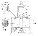
- a liquid reservoir 10 between the projection system and the substrateis bounded by a gas seal 16 forming an annulus around the projection system.
- the seal 16in an embodiment a gas seal, is formed by gas e.g. air, synthetic air, N 2 or an inert gas, provided under pressure via inlet 15 to the gap between seal member 12 and the substrate and extracted via first outlet 14 .
- gase.g. air, synthetic air, N 2 or an inert gas
- the over pressure on the gas inlet 15 , vacuum level on the first outlet 14 and geometry of the gapare arranged so that there is a high velocity gas flow inwards that confines the liquid.
- the distance between the gas inlet and outlet and substrate Wis small.
- the liquid reservoiris supplied with liquid by inlet 22 and extends above the bottom of the final element of the projection system PL. Excess liquid is removed via outlet 14 .
- metal membranesmay be used to confine the humid gas between the projection system and a liquid confinement structure used to at least partly contain the liquid between the projection system and the substrate.
- rubber-like Viton fluoroelastomer ringsmay be used to confine the gas. In such arrangements, however, it may be possible a vibration is transmitted between the projection system and the liquid confinement structure.
- the projection systemalso comprises a cover 35 attached to a main part of the projection system PL by a seal 40 .
- the seal 40should be flexible to accommodate small relative movement between the main part of the projection system PL and the cover 35 . Glues are likely to be particularly effective. An advantage of such an arrangement is transmission of vibration forces between the projection system and the liquid confinement structure may be reduced or avoided.
- a vacuum chamber 34 with an inlet 33is arranged in the volume above the reservoir 10 .
- the outside of the vacuum chamber 34 and cover 35form a passage 32 along which gas flows towards vacuum chamber 34 .
- gas from all surrounding areaswill flow towards the vacuum chamber 34 .
- the partial vapor pressure of the liquid in the gas above the reservoir 10is high, and the flow of gas along passage 32 prevents the humid gas from entering the projection system PL.
- the gas flowwill absorb humidity from surrounding gas so there is a gradient of humidity, the humidity of the gas decreasing away from the reservoir 10 .
- delicate parts of the apparatussuch as mirrors for the interferometer beams are arranged in a dry part of the apparatus so that the humidity doesn't affect measurements made using the interferometer beams.
- glueis used as seal 40 , dry, flowing gas will help to ensure that the glue remains dry and therefore a gastight seal is maintained. Keeping the glue 40 dry also helps prevent it from expanding and thus generating forces which may deform the projection system.
- the vacuum chamber 34can be independent of the projection system as in the example above, or can be part of the projection system PL, or part of the seal member 12 and in any of these circumstances may be actuatable in the Z direction.
- the example hereis of a vacuum chamber i.e. an underpressure generating a gas flow, the gas flow port could equally comprise an overpressure.
- a system as described abovemay be used in conjunction with the liquid supply system shown in FIGS. 2 and 3 , the vacuum chamber 34 and passage 32 being arranged above the inlets IN and outlets OUT.
Landscapes
- Physics & Mathematics (AREA)
- General Physics & Mathematics (AREA)
- Exposure And Positioning Against Photoresist Photosensitive Materials (AREA)
- Exposure Of Semiconductors, Excluding Electron Or Ion Beam Exposure (AREA)
Abstract
Description
- an illumination system configured to condition beam of radiation;
- a support structure configured to hold a patterning device, the patterning device configured to pattern the beam of radiation according to a desired pattern;
- a substrate table configured to hold a substrate;
- a projection system configured to project the patterned beam onto a target portion of the substrate;
- a liquid supply system configured to at least partly fill a space between the projection system and the substrate with a liquid; and
- a gas flow port configured to create a flow of gas to remove humid gas in a space above and in contact with the liquid, to confine the humid gas in the space, or both.
- providing a liquid to a space between a projection system and a substrate;
- flowing a gas in a space above and in contact the liquid to remove humid gas in the space, to confine the humid gas in the space, or both; and
- projecting a patterned beam of radiation using the projection system onto a target portion of the substrate through the liquid.
- an illumination system (illuminator) IL configured to provide a projection beam PB of radiation (e.g. UV radiation).
- a first support structure (e.g. a mask table) MT configured to hold a patterning device (e.g. a mask) MA and connected to a first positioner PM configured to accurately position the patterning device with respect to item PL;
- a substrate table (e.g. a wafer table) WT configured to hold a substrate (e.g. a resist-coated wafer) W and connected to a second positioner PW configured to accurately position the substrate with respect to item PL; and
- a projection system (e.g. a refractive projection lens) PL configured to image a pattern imparted to the projection beam PB by patterning device MA onto a target portion C (e.g. comprising one or more dies) of the substrate W.
- 1. In step mode, the mask table MT and the substrate table WT are kept essentially stationary, while an entire pattern imparted to the projection beam is projected onto a target portion C at one time (i.e. a single static exposure). The substrate table WT is then shifted in the X and/or Y direction so that a different target portion C can be exposed. In step mode, the maximum size of the exposure field limits the size of the target portion C imaged in a single static exposure.
- 2. In scan mode, the mask table MT and the substrate table WT are scanned synchronously while a pattern imparted to the projection beam is projected onto a target portion C (i.e. a single dynamic exposure). The velocity and direction of the substrate table WT relative to the mask table MT is determined by the (de-)magnification and image reversal characteristics of the projection system PL. In scan mode, the maximum size of the exposure field limits the width (in the non-scanning direction) of the target portion in a single dynamic exposure, whereas the length of the scanning motion determines the height (in the scanning direction) of the target portion.
- 3. In another mode, the mask table MT is kept essentially stationary holding a programmable patterning device, and the substrate table WT is moved or scanned while a pattern imparted to the projection beam is projected onto a target portion C. In this mode, generally a pulsed radiation source is employed and the programmable patterning device is updated as required after each movement of the substrate table WT or in between successive radiation pulses during a scan. This mode of operation can be readily applied to maskless lithography that utilizes a programmable patterning device, such as a programmable mirror array of a type as referred to above.
Claims (35)
Priority Applications (5)
| Application Number | Priority Date | Filing Date | Title |
|---|---|---|---|
| US12/010,705US7532304B2 (en) | 2003-10-28 | 2008-01-29 | Lithographic apparatus and device manufacturing method |
| US12/422,140US8102502B2 (en) | 2003-10-28 | 2009-04-10 | Lithographic apparatus and device manufacturing method |
| US13/323,404US8810771B2 (en) | 2003-10-28 | 2011-12-12 | Lithographic apparatus and device manufacturing method |
| US13/356,231US8860922B2 (en) | 2003-10-28 | 2012-01-23 | Lithographic apparatus and device manufacturing method |
| US14/504,191US9182679B2 (en) | 2003-10-28 | 2014-10-01 | Lithographic apparatus and device manufacturing method |
Applications Claiming Priority (3)
| Application Number | Priority Date | Filing Date | Title |
|---|---|---|---|
| EP03256809 | 2003-10-28 | ||
| EP03256809 | 2003-10-28 | ||
| EP03256809.9 | 2003-10-28 |
Related Child Applications (1)
| Application Number | Title | Priority Date | Filing Date |
|---|---|---|---|
| US12/010,705ContinuationUS7532304B2 (en) | 2003-10-28 | 2008-01-29 | Lithographic apparatus and device manufacturing method |
Publications (2)
| Publication Number | Publication Date |
|---|---|
| US20050128445A1 US20050128445A1 (en) | 2005-06-16 |
| US7352433B2true US7352433B2 (en) | 2008-04-01 |
Family
ID=34639339
Family Applications (6)
| Application Number | Title | Priority Date | Filing Date |
|---|---|---|---|
| US10/961,395Expired - LifetimeUS7352433B2 (en) | 2003-10-28 | 2004-10-12 | Lithographic apparatus and device manufacturing method |
| US12/010,705Expired - LifetimeUS7532304B2 (en) | 2003-10-28 | 2008-01-29 | Lithographic apparatus and device manufacturing method |
| US12/422,140Expired - Fee RelatedUS8102502B2 (en) | 2003-10-28 | 2009-04-10 | Lithographic apparatus and device manufacturing method |
| US13/323,404Expired - Fee RelatedUS8810771B2 (en) | 2003-10-28 | 2011-12-12 | Lithographic apparatus and device manufacturing method |
| US13/356,231Expired - Fee RelatedUS8860922B2 (en) | 2003-10-28 | 2012-01-23 | Lithographic apparatus and device manufacturing method |
| US14/504,191Expired - Fee RelatedUS9182679B2 (en) | 2003-10-28 | 2014-10-01 | Lithographic apparatus and device manufacturing method |
Family Applications After (5)
| Application Number | Title | Priority Date | Filing Date |
|---|---|---|---|
| US12/010,705Expired - LifetimeUS7532304B2 (en) | 2003-10-28 | 2008-01-29 | Lithographic apparatus and device manufacturing method |
| US12/422,140Expired - Fee RelatedUS8102502B2 (en) | 2003-10-28 | 2009-04-10 | Lithographic apparatus and device manufacturing method |
| US13/323,404Expired - Fee RelatedUS8810771B2 (en) | 2003-10-28 | 2011-12-12 | Lithographic apparatus and device manufacturing method |
| US13/356,231Expired - Fee RelatedUS8860922B2 (en) | 2003-10-28 | 2012-01-23 | Lithographic apparatus and device manufacturing method |
| US14/504,191Expired - Fee RelatedUS9182679B2 (en) | 2003-10-28 | 2014-10-01 | Lithographic apparatus and device manufacturing method |
Country Status (7)
| Country | Link |
|---|---|
| US (6) | US7352433B2 (en) |
| JP (1) | JP4146828B2 (en) |
| KR (1) | KR100632891B1 (en) |
| CN (1) | CN1612051B (en) |
| DE (1) | DE602004025893D1 (en) |
| SG (1) | SG111309A1 (en) |
| TW (1) | TWI263261B (en) |
Cited By (5)
| Publication number | Priority date | Publication date | Assignee | Title |
|---|---|---|---|---|
| US20050259234A1 (en)* | 2002-12-10 | 2005-11-24 | Nikon Corporation | Exposure apparatus and device manufacturing method |
| US20070220775A1 (en)* | 2006-03-22 | 2007-09-27 | Katsuhiko Miya | Substrate processing method and substrate processing apparatus |
| US20100259737A1 (en)* | 2004-02-19 | 2010-10-14 | Nikon Corporation | Exposure apparatus preventing gas from moving from exposure region to measurement region |
| US20120086926A1 (en)* | 2003-10-28 | 2012-04-12 | Carl Zeiss Smt Ag | Lithographic apparatus and device manufacturing method |
| US10095129B2 (en) | 2014-07-04 | 2018-10-09 | Asml Netherlands B.V. | Lithographic apparatus and a method of manufacturing a device using a lithographic apparatus |
Families Citing this family (27)
| Publication number | Priority date | Publication date | Assignee | Title |
|---|---|---|---|---|
| KR101225884B1 (en)* | 2003-04-11 | 2013-01-28 | 가부시키가이샤 니콘 | Apparatus and method for maintaining immersion fluid in the gap under the projection lens during wafer exchange in an immersion lithography machine |
| KR101242815B1 (en) | 2003-06-13 | 2013-03-12 | 가부시키가이샤 니콘 | Exposure method, substrate stage, exposure apparatus and method for manufacturing device |
| TW201721717A (en) | 2003-06-19 | 2017-06-16 | 尼康股份有限公司 | Exposure apparatus, exposure method, and device manufacturing method |
| TWI553701B (en) | 2003-10-09 | 2016-10-11 | 尼康股份有限公司 | Exposure apparatus and exposure method, component manufacturing method |
| KR101394764B1 (en) | 2003-12-03 | 2014-05-27 | 가부시키가이샤 니콘 | Exposure apparatus, exposure method, device producing method, and optical component |
| US20070081133A1 (en)* | 2004-12-14 | 2007-04-12 | Niikon Corporation | Projection exposure apparatus and stage unit, and exposure method |
| JP4720506B2 (en) | 2003-12-15 | 2011-07-13 | 株式会社ニコン | Stage apparatus, exposure apparatus, and exposure method |
| JPWO2005057635A1 (en)* | 2003-12-15 | 2007-07-05 | 株式会社ニコン | Projection exposure apparatus, stage apparatus, and exposure method |
| US7589822B2 (en) | 2004-02-02 | 2009-09-15 | Nikon Corporation | Stage drive method and stage unit, exposure apparatus, and device manufacturing method |
| KR101506100B1 (en)* | 2004-09-17 | 2015-03-26 | 가부시키가이샤 니콘 | Exposure apparatus, exposure method, and method for manufacturing device |
| JP4072543B2 (en)* | 2005-03-18 | 2008-04-09 | キヤノン株式会社 | Immersion exposure apparatus and device manufacturing method |
| USRE43576E1 (en) | 2005-04-08 | 2012-08-14 | Asml Netherlands B.V. | Dual stage lithographic apparatus and device manufacturing method |
| US7317507B2 (en)* | 2005-05-03 | 2008-01-08 | Asml Netherlands B.V. | Lithographic apparatus and device manufacturing method |
| US7834974B2 (en)* | 2005-06-28 | 2010-11-16 | Asml Netherlands B.V. | Lithographic apparatus and device manufacturing method |
| JP2007142366A (en) | 2005-10-18 | 2007-06-07 | Canon Inc | Exposure apparatus and device manufacturing method |
| US8125610B2 (en)* | 2005-12-02 | 2012-02-28 | ASML Metherlands B.V. | Method for preventing or reducing contamination of an immersion type projection apparatus and an immersion type lithographic apparatus |
| CN100590173C (en)* | 2006-03-24 | 2010-02-17 | 北京有色金属研究总院 | A kind of fluorescent powder and its manufacturing method and the made electric light source |
| US9477158B2 (en)* | 2006-04-14 | 2016-10-25 | Asml Netherlands B.V. | Lithographic apparatus and device manufacturing method |
| JP5182093B2 (en)* | 2006-09-06 | 2013-04-10 | 株式会社ニコン | Optical apparatus, exposure apparatus, and device manufacturing method |
| US8654305B2 (en)* | 2007-02-15 | 2014-02-18 | Asml Holding N.V. | Systems and methods for insitu lens cleaning in immersion lithography |
| NL1035908A1 (en)* | 2007-09-25 | 2009-03-26 | Asml Netherlands Bv | Lithographic apparatus and device manufacturing method. |
| US9176393B2 (en) | 2008-05-28 | 2015-11-03 | Asml Netherlands B.V. | Lithographic apparatus and a method of operating the apparatus |
| NL2003392A (en)* | 2008-09-17 | 2010-03-18 | Asml Netherlands Bv | Lithographic apparatus and a method of operating the apparatus. |
| TWI457714B (en)* | 2008-09-17 | 2014-10-21 | Asml Netherlands Bv | Lithographic apparatus and a method of operating the apparatus |
| US8953143B2 (en)* | 2009-04-24 | 2015-02-10 | Nikon Corporation | Liquid immersion member |
| NL2004497A (en) | 2009-05-01 | 2010-11-02 | Asml Netherlands Bv | Lithographic apparatus and a method of operating the apparatus. |
| CN108778927A (en)* | 2015-09-23 | 2018-11-09 | 沃尔玛阿波罗有限责任公司 | The system and method for delivering product with unmanned delivery aircraft |
Citations (139)
| Publication number | Priority date | Publication date | Assignee | Title |
|---|---|---|---|---|
| DE242880C (en) | ||||
| DE224448C (en) | ||||
| DE221563C (en) | ||||
| DE206607C (en) | ||||
| US3573975A (en) | 1968-07-10 | 1971-04-06 | Ibm | Photochemical fabrication process |
| US3648587A (en) | 1967-10-20 | 1972-03-14 | Eastman Kodak Co | Focus control for optical instruments |
| EP0023231A1 (en) | 1979-07-27 | 1981-02-04 | Tabarelli, Werner, Dr. | Optical lithographic method and apparatus for copying a pattern onto a semiconductor wafer |
| FR2474708A1 (en) | 1980-01-24 | 1981-07-31 | Dme | Micro:photo:lithographic process giving high line resolution - with application of immersion oil between mask and photosensitive layer before exposure |
| US4346164A (en) | 1980-10-06 | 1982-08-24 | Werner Tabarelli | Photolithographic method for the manufacture of integrated circuits |
| JPS57153433A (en) | 1981-03-18 | 1982-09-22 | Hitachi Ltd | Manufacturing device for semiconductor |
| US4390273A (en) | 1981-02-17 | 1983-06-28 | Censor Patent-Und Versuchsanstalt | Projection mask as well as a method and apparatus for the embedding thereof and projection printing system |
| US4396705A (en) | 1980-09-19 | 1983-08-02 | Hitachi, Ltd. | Pattern forming method and pattern forming apparatus using exposures in a liquid |
| JPS58202448A (en) | 1982-05-21 | 1983-11-25 | Hitachi Ltd | exposure equipment |
| JPS5919912A (en) | 1982-07-26 | 1984-02-01 | Hitachi Ltd | Immersion distance holding device |
| US4509852A (en) | 1980-10-06 | 1985-04-09 | Werner Tabarelli | Apparatus for the photolithographic manufacture of integrated circuit elements |
| JPS6265326A (en) | 1985-09-18 | 1987-03-24 | Hitachi Ltd | Exposure device |
| JPS62121417A (en) | 1985-11-22 | 1987-06-02 | Hitachi Ltd | Immersion objective lens device |
| JPS63157419A (en) | 1986-12-22 | 1988-06-30 | Toshiba Corp | Fine pattern transfer apparatus |
| EP0418427A2 (en) | 1989-09-06 | 1991-03-27 | Eiichi Miyake | Exposure process |
| US5040020A (en) | 1988-03-31 | 1991-08-13 | Cornell Research Foundation, Inc. | Self-aligned, high resolution resonant dielectric lithography |
| JPH04305915A (en) | 1991-04-02 | 1992-10-28 | Nikon Corp | Adhesion type exposure device |
| JPH04305917A (en) | 1991-04-02 | 1992-10-28 | Nikon Corp | Close-contact exposure equipment |
| JPH0562877A (en) | 1991-09-02 | 1993-03-12 | Yasuko Shinohara | Optical system for lsi manufacturing contraction projection aligner by light |
| JPH05304072A (en) | 1992-04-08 | 1993-11-16 | Nec Corp | Manufacture of semiconductor device |
| JPH06124873A (en) | 1992-10-09 | 1994-05-06 | Canon Inc | Immersion projection exposure system |
| JPH07132262A (en) | 1992-12-21 | 1995-05-23 | Tokyo Electron Ltd | Liquid treating device of immersion type |
| JPH07220990A (en) | 1994-01-28 | 1995-08-18 | Hitachi Ltd | Pattern forming method and exposure apparatus thereof |
| US5610683A (en) | 1992-11-27 | 1997-03-11 | Canon Kabushiki Kaisha | Immersion type projection exposure apparatus |
| US5715039A (en) | 1995-05-19 | 1998-02-03 | Hitachi, Ltd. | Projection exposure apparatus and method which uses multiple diffraction gratings in order to produce a solid state device with fine patterns |
| EP0834773A2 (en) | 1996-10-07 | 1998-04-08 | Nikon Corporation | Focusing and tilting adjustment system for lithography aligner, manufacturing apparatus or inspection apparatus |
| JPH10228661A (en) | 1997-02-14 | 1998-08-25 | Sony Corp | Master disk manufacturing aligner for optical recording medium |
| JPH10255319A (en) | 1997-03-12 | 1998-09-25 | Hitachi Maxell Ltd | Master exposure apparatus and method |
| JPH10303114A (en) | 1997-04-23 | 1998-11-13 | Nikon Corp | Immersion type exposure equipment |
| JPH10340846A (en) | 1997-06-10 | 1998-12-22 | Nikon Corp | Aligner, its manufacture, exposing method and device manufacturing method |
| US5900354A (en) | 1997-07-03 | 1999-05-04 | Batchelder; John Samuel | Method for optical inspection and lithography |
| JPH11176727A (en) | 1997-12-11 | 1999-07-02 | Nikon Corp | Projection exposure equipment |
| WO1999049504A1 (en) | 1998-03-26 | 1999-09-30 | Nikon Corporation | Projection exposure method and system |
| US5997963A (en)* | 1998-05-05 | 1999-12-07 | Ultratech Stepper, Inc. | Microchamber |
| JP2000058436A (en) | 1998-08-11 | 2000-02-25 | Nikon Corp | Projection exposure apparatus and exposure method |
| EP1039511A1 (en) | 1997-12-12 | 2000-09-27 | Nikon Corporation | Projection exposure method and projection aligner |
| JP2001091849A (en) | 1999-09-21 | 2001-04-06 | Olympus Optical Co Ltd | Immersion objective lens for microscope |
| US6236634B1 (en) | 1996-08-26 | 2001-05-22 | Digital Papyrus Corporation | Method and apparatus for coupling an optical lens to a disk through a coupling medium having a relatively high index of refraction |
| US20010038442A1 (en)* | 2000-05-03 | 2001-11-08 | Silicon Valley Group, Inc. | Method and apparatus for a non-contact scavenging seal |
| US20020020821A1 (en) | 2000-08-08 | 2002-02-21 | Koninklijke Philips Electronics N.V. | Method of manufacturing an optically scannable information carrier |
| US20020163629A1 (en) | 2001-05-07 | 2002-11-07 | Michael Switkes | Methods and apparatus employing an index matching medium |
| US20030030916A1 (en) | 2000-12-11 | 2003-02-13 | Nikon Corporation | Projection optical system and exposure apparatus having the projection optical system |
| US6560032B2 (en) | 2000-03-27 | 2003-05-06 | Olympus Optical Co., Ltd. | Liquid immersion lens system and optical apparatus using the same |
| US20030123040A1 (en) | 2001-11-07 | 2003-07-03 | Gilad Almogy | Optical spot grid array printer |
| US20030123042A1 (en)* | 2000-02-10 | 2003-07-03 | Joseph Laganza | Method and apparatus for a reticle with purged pellicle-to-reticle gap |
| US6600547B2 (en) | 2001-09-24 | 2003-07-29 | Nikon Corporation | Sliding seal |
| US6603130B1 (en) | 1999-04-19 | 2003-08-05 | Asml Netherlands B.V. | Gas bearings for use with vacuum chambers and their application in lithographic projection apparatuses |
| US20030146396A1 (en)* | 1999-11-05 | 2003-08-07 | Asml Netherlands B.V. | Gas flushing system with recovery system for use in lithographic apparatus |
| US20030174408A1 (en) | 2002-03-08 | 2003-09-18 | Carl Zeiss Smt Ag | Refractive projection objective for immersion lithography |
| WO2003077034A2 (en) | 2002-03-06 | 2003-09-18 | E.I. Du Pont De Nemours And Company | Fluorine-containing compounds with high transparency in the vacuum ultraviolet |
| WO2003085708A1 (en) | 2002-04-09 | 2003-10-16 | Nikon Corporation | Exposure method, exposure device, and device manufacturing method |
| US20040000627A1 (en) | 2002-06-28 | 2004-01-01 | Carl Zeiss Semiconductor Manufacturing Technologies Ag | Method for focus detection and an imaging system with a focus-detection system |
| US20040075895A1 (en) | 2002-10-22 | 2004-04-22 | Taiwan Semiconductor Manufacturing Co., Ltd. | Apparatus for method for immersion lithography |
| EP1420298A2 (en) | 2002-11-12 | 2004-05-19 | ASML Netherlands B.V. | Immersion lithographic apparatus and device manufacturing method |
| US20040109237A1 (en) | 2002-12-09 | 2004-06-10 | Carl Zeiss Smt Ag | Projection objective, especially for microlithography, and method for adjusting a projection objective |
| US20040114117A1 (en) | 2002-11-18 | 2004-06-17 | Asml Netherlands B.V. | Lithographic apparatus and device manufacturing method |
| US20040119954A1 (en) | 2002-12-10 | 2004-06-24 | Miyoko Kawashima | Exposure apparatus and method |
| WO2004053954A1 (en) | 2002-12-10 | 2004-06-24 | Nikon Corporation | Exposure apparatus and method for manufacturing device |
| WO2004053956A1 (en) | 2002-12-10 | 2004-06-24 | Nikon Corporation | Exposure apparatus, exposure method and method for manufacturing device |
| WO2004053955A1 (en) | 2002-12-10 | 2004-06-24 | Nikon Corporation | Exposure system and device producing method |
| WO2004053950A1 (en) | 2002-12-10 | 2004-06-24 | Nikon Corporation | Exposure apparatus and method for manufacturing device |
| WO2004053959A1 (en) | 2002-12-10 | 2004-06-24 | Nikon Corporation | Optical device and projection exposure apparatus using such optical device |
| WO2004053951A1 (en) | 2002-12-10 | 2004-06-24 | Nikon Corporation | Exposure method, exposure apparatus and method for manufacturing device |
| WO2004053958A1 (en) | 2002-12-10 | 2004-06-24 | Nikon Corporation | Exposure apparatus and method for manufacturing device |
| US20040118184A1 (en) | 2002-12-19 | 2004-06-24 | Asml Holding N.V. | Liquid flow proximity sensor for use in immersion lithography |
| WO2004053953A1 (en) | 2002-12-10 | 2004-06-24 | Nikon Corporation | Exposure apparatus and method for manufacturing device |
| WO2004053952A1 (en) | 2002-12-10 | 2004-06-24 | Nikon Corporation | Exposure apparatus and method for manufacturing device |
| WO2004053957A1 (en) | 2002-12-10 | 2004-06-24 | Nikon Corporation | Surface position detection apparatus, exposure method, and device porducing method |
| WO2004053596A2 (en) | 2002-12-10 | 2004-06-24 | Carl Zeiss Smt Ag | Method for adjusting a desired optical property of a positioning lens and microlithographic projection exposure system |
| WO2004055803A1 (en) | 2002-12-13 | 2004-07-01 | Koninklijke Philips Electronics N.V. | Liquid removal in a method and device for irradiating spots on a layer |
| US20040125351A1 (en) | 2002-12-30 | 2004-07-01 | Krautschik Christof Gabriel | Immersion lithography |
| WO2004057590A1 (en) | 2002-12-19 | 2004-07-08 | Koninklijke Philips Electronics N.V. | Method and device for irradiating spots on a layer |
| JP2004193252A (en) | 2002-12-10 | 2004-07-08 | Nikon Corp | Exposure method and device manufacturing method |
| WO2004057589A1 (en) | 2002-12-19 | 2004-07-08 | Koninklijke Philips Electronics N.V. | Method and device for irradiating spots on a layer |
| US20040136494A1 (en) | 2002-11-12 | 2004-07-15 | Asml Netherlands B.V. | Lithographic apparatus and device manufacturing method |
| US20040160582A1 (en) | 2002-11-12 | 2004-08-19 | Asml Netherlands B.V. | Lithographic apparatus and device manufacturing method |
| US20040165159A1 (en) | 2002-11-12 | 2004-08-26 | Asml Netherlands B.V. | Lithographic apparatus and device manufacturing method |
| US20040169924A1 (en) | 2003-02-27 | 2004-09-02 | Asml Netherlands, B.V. | Stationary and dynamic radial transverse electric polarizer for high numerical aperture systems |
| US20040169834A1 (en) | 2002-11-18 | 2004-09-02 | Infineon Technologies Ag | Optical device for use with a lithography method |
| WO2004077154A2 (en) | 2003-02-21 | 2004-09-10 | Asml Holding N.V. | Lithographic printing with polarized light |
| US20040180299A1 (en) | 2003-03-11 | 2004-09-16 | Rolland Jason P. | Immersion lithography methods using carbon dioxide |
| WO2004090577A2 (en) | 2003-04-11 | 2004-10-21 | Nikon Corporation | Maintaining immersion fluid under a lithographic projection lens |
| WO2004090633A2 (en) | 2003-04-10 | 2004-10-21 | Nikon Corporation | An electro-osmotic element for an immersion lithography apparatus |
| US20040207824A1 (en) | 2002-11-12 | 2004-10-21 | Asml Netherlands B.V. | Lithographic apparatus and device manufacturing method |
| WO2004090634A2 (en) | 2003-04-10 | 2004-10-21 | Nikon Corporation | Environmental system including vaccum scavange for an immersion lithography apparatus |
| WO2004019128A3 (en) | 2002-08-23 | 2004-10-28 | Nippon Kogaku Kk | Projection optical system and method for photolithography and exposure apparatus and method using same |
| US20040211920A1 (en) | 2002-11-12 | 2004-10-28 | Asml Netherlands B.V. | Lithographic apparatus and device manufacturing method |
| WO2004093160A2 (en) | 2003-04-10 | 2004-10-28 | Nikon Corporation | Run-off path to collect liquid for an immersion lithography apparatus |
| WO2004093159A2 (en) | 2003-04-09 | 2004-10-28 | Nikon Corporation | Immersion lithography fluid control system |
| WO2004092833A2 (en) | 2003-04-10 | 2004-10-28 | Nikon Corporation | Environmental system including a transport region for an immersion lithography apparatus |
| WO2004092830A2 (en) | 2003-04-11 | 2004-10-28 | Nikon Corporation | Liquid jet and recovery system for immersion lithography |
| WO2004093130A2 (en) | 2003-04-11 | 2004-10-28 | Nikon Corporation | Cleanup method for optics in immersion lithography |
| WO2004095135A2 (en) | 2003-04-17 | 2004-11-04 | Nikon Corporation | Optical arrangement of autofocus elements for use with immersion lithography |
| US20040224525A1 (en) | 2003-05-09 | 2004-11-11 | Matsushita Electric Industrial Co., Ltd. | Pattern formation method |
| US20040224265A1 (en) | 2003-05-09 | 2004-11-11 | Matsushita Electric Industrial Co., Ltd | Pattern formation method and exposure system |
| US20040227923A1 (en) | 2003-02-27 | 2004-11-18 | Flagello Donis George | Stationary and dynamic radial transverse electric polarizer for high numerical aperture systems |
| US20040253547A1 (en) | 2003-06-12 | 2004-12-16 | Matsushita Electric Industrial Co., Ltd. | Pattern formation method |
| US20040253548A1 (en) | 2003-06-12 | 2004-12-16 | Matsushita Electric Industrial Co., Ltd. | Pattern formation method |
| US20040259008A1 (en) | 2003-06-23 | 2004-12-23 | Matsushita Electric Industrial Co., Ltd. | Pattern formation method |
| US20040257544A1 (en)* | 2003-06-19 | 2004-12-23 | Asml Holding N.V. | Immersion photolithography system and method using microchannel nozzles |
| US20040259040A1 (en) | 2003-06-23 | 2004-12-23 | Matsushita Electric Industrial Co., Ltd. | Pattern formation method |
| US20040263808A1 (en) | 2003-06-27 | 2004-12-30 | Asml Holding N.V. | Immersion photolithography system and method using inverted wafer-projection optics interface |
| WO2005001432A2 (en) | 2003-03-24 | 2005-01-06 | Massachusetts Institute Of Technology | Optical fluids, and systems and methods of making and using the same |
| WO2005003864A2 (en) | 2003-06-24 | 2005-01-13 | Lam Research Corporation | Apparatus and method for providing a confined liquid for immersion lithography |
| WO2005006417A1 (en) | 2003-07-09 | 2005-01-20 | Nikon Corporation | Exposure apparatus and method for manufacturing device |
| WO2005006026A2 (en) | 2003-07-01 | 2005-01-20 | Nikon Corporation | Using isotopically specified fluids as optical elements |
| WO2005008339A2 (en) | 2003-07-21 | 2005-01-27 | Asml Netherlands B.V. | Lithographic projection apparatus, purge gas supply system and gas purging method |
| US20050018156A1 (en) | 2003-06-30 | 2005-01-27 | Asml Netherlands B.V. | Lithographic apparatus and device manufacturing method |
| WO2005013008A2 (en) | 2003-07-25 | 2005-02-10 | Advanced Micro Devices, Inc. | Method for monitoring and controlling imaging in immersion lithography systems |
| US20050030506A1 (en) | 2002-03-08 | 2005-02-10 | Carl Zeiss Smt Ag | Projection exposure method and projection exposure system |
| US20050036121A1 (en) | 2002-11-12 | 2005-02-17 | Asml Netherlands B.V. | Lithographic apparatus and device manufacturing method |
| US20050036213A1 (en) | 2003-08-12 | 2005-02-17 | Hans-Jurgen Mann | Projection objectives including a plurality of mirrors with lenses ahead of mirror M3 |
| US20050036184A1 (en) | 2003-08-11 | 2005-02-17 | Yee-Chia Yeo | Lithography apparatus for manufacture of integrated circuits |
| US20050036183A1 (en) | 2003-08-11 | 2005-02-17 | Yee-Chia Yeo | Immersion fluid for immersion Lithography, and method of performing immersion lithography |
| US20050037269A1 (en) | 2003-08-11 | 2005-02-17 | Levinson Harry J. | Method and apparatus for monitoring and controlling imaging in immersion lithography systems |
| US20050046934A1 (en) | 2003-08-29 | 2005-03-03 | Tokyo Electron Limited | Method and system for drying a substrate |
| WO2005019935A2 (en) | 2003-08-21 | 2005-03-03 | Advanced Micro Devices, Inc. | Refractive index system monitor and control for immersion lithography |
| US20050048223A1 (en) | 2003-09-02 | 2005-03-03 | Pawloski Adam R. | Method and apparatus for elimination of bubbles in immersion medium in immersion lithography systems |
| WO2005024517A2 (en) | 2003-09-03 | 2005-03-17 | Nikon Corporation | Apparatus and method for providing fluid for immersion lithography |
| US20050068639A1 (en) | 2003-09-26 | 2005-03-31 | Fortis Systems Inc. | Contact printing using a magnified mask image |
| US20050073670A1 (en) | 2003-10-03 | 2005-04-07 | Micronic Laser Systems Ab | Method and device for immersion lithography |
| US20050084794A1 (en) | 2003-10-16 | 2005-04-21 | Meagley Robert P. | Methods and compositions for providing photoresist with improved properties for contacting liquids |
| US20050094116A1 (en) | 2003-08-29 | 2005-05-05 | Asml Netherlands B.V. | Gradient immersion lithography |
| US20050100745A1 (en) | 2003-11-06 | 2005-05-12 | Taiwan Semiconductor Manufacturing Company, Ltd. | Anti-corrosion layer on objective lens for liquid immersion lithography applications |
| US20050110973A1 (en) | 2003-11-24 | 2005-05-26 | Asml Netherlands B.V. | Lithographic apparatus and device manufacturing method |
| US20050117224A1 (en) | 1999-12-29 | 2005-06-02 | Carl Zeiss Smt Ag | Catadioptric projection objective with geometric beam splitting |
| US20050122497A1 (en) | 2003-12-03 | 2005-06-09 | Lyons Christopher F. | Immersion lithographic process using a conforming immersion medium |
| WO2005054953A2 (en) | 2003-11-24 | 2005-06-16 | Carl-Zeiss Smt Ag | Holding device for an optical element in an objective |
| US20050128445A1 (en) | 2003-10-28 | 2005-06-16 | Asml Netherlands B.V. | Lithographic apparatus and device manufacturing method |
| US20050134817A1 (en) | 2003-06-25 | 2005-06-23 | Takashi Nakamura | Liquid immersion type exposure apparatus |
| US20050190455A1 (en) | 1999-12-29 | 2005-09-01 | Carl Zeiss Smt Ag | Refractive projection objective for immersion lithography |
| US20050217135A1 (en) | 2002-09-30 | 2005-10-06 | Lam Research Corp. | Phobic barrier meniscus separation and containment |
| US20050217137A1 (en) | 2002-09-30 | 2005-10-06 | Lam Research Corp. | Concentric proximity processing head |
| US20050217703A1 (en) | 2002-09-30 | 2005-10-06 | Lam Research Corp. | Apparatus and method for utilizing a meniscus in substrate processing |
| US20060114445A1 (en) | 2003-06-19 | 2006-06-01 | Nikon Corporation | Exposure apparatus, and device manufacturing method |
Family Cites Families (16)
| Publication number | Priority date | Publication date | Assignee | Title |
|---|---|---|---|---|
| JPS5919912Y2 (en) | 1978-08-21 | 1984-06-08 | 清水建設株式会社 | composite heat exchanger |
| DD160756A3 (en)* | 1981-04-24 | 1984-02-29 | Gudrun Dietz | ARRANGEMENT FOR IMPROVING PHOTOCHEMICAL IMPLEMENTATION PROCESSES IN PHOTORESIS LAYERS |
| DD206607A1 (en) | 1982-06-16 | 1984-02-01 | Mikroelektronik Zt Forsch Tech | METHOD AND DEVICE FOR ELIMINATING INTERFERENCE EFFECTS |
| DD242880A1 (en) | 1983-01-31 | 1987-02-11 | Kuch Karl Heinz | DEVICE FOR PHOTOLITHOGRAPHIC STRUCTURAL TRANSMISSION |
| DD221563A1 (en) | 1983-09-14 | 1985-04-24 | Mikroelektronik Zt Forsch Tech | IMMERSIONS OBJECTIVE FOR THE STEP-BY-STEP PROJECTION IMAGING OF A MASK STRUCTURE |
| DD224448A1 (en) | 1984-03-01 | 1985-07-03 | Zeiss Jena Veb Carl | DEVICE FOR PHOTOLITHOGRAPHIC STRUCTURAL TRANSMISSION |
| DE3447488A1 (en) | 1984-10-19 | 1986-05-07 | Canon K.K., Tokio/Tokyo | PROJECTION DEVICE |
| JPS6265326U (en) | 1985-10-16 | 1987-04-23 | ||
| JPS62121417U (en) | 1986-01-24 | 1987-08-01 | ||
| JPS63157419U (en) | 1987-03-31 | 1988-10-14 | ||
| JPH0678192B2 (en) | 1991-10-03 | 1994-10-05 | 工業技術院長 | Carbon-silicon carbide based composite material and method for producing the same |
| JP2004259786A (en) | 2003-02-24 | 2004-09-16 | Canon Inc | Exposure equipment |
| KR20050110033A (en) | 2003-03-25 | 2005-11-22 | 가부시키가이샤 니콘 | Exposure system and device production method |
| EP1498778A1 (en) | 2003-06-27 | 2005-01-19 | ASML Netherlands B.V. | Lithographic apparatus and device manufacturing method |
| EP1519231B1 (en) | 2003-09-29 | 2005-12-21 | ASML Netherlands B.V. | Lithographic apparatus and device manufacturing method |
| AU2004203138B2 (en) | 2004-07-13 | 2011-08-04 | Robert William Cox | Golf swing training apparatus |
- 2004
- 2004-10-12USUS10/961,395patent/US7352433B2/ennot_activeExpired - Lifetime
- 2004-10-15TWTW93131422Apatent/TWI263261B/ennot_activeIP Right Cessation
- 2004-10-22SGSG200406939Apatent/SG111309A1/enunknown
- 2004-10-26DEDE200460025893patent/DE602004025893D1/ennot_activeExpired - Lifetime
- 2004-10-27KRKR20040086237Apatent/KR100632891B1/ennot_activeExpired - Fee Related
- 2004-10-27CNCN 200410087957patent/CN1612051B/ennot_activeExpired - Lifetime
- 2004-10-27JPJP2004312062Apatent/JP4146828B2/ennot_activeExpired - Fee Related
- 2008
- 2008-01-29USUS12/010,705patent/US7532304B2/ennot_activeExpired - Lifetime
- 2009
- 2009-04-10USUS12/422,140patent/US8102502B2/ennot_activeExpired - Fee Related
- 2011
- 2011-12-12USUS13/323,404patent/US8810771B2/ennot_activeExpired - Fee Related
- 2012
- 2012-01-23USUS13/356,231patent/US8860922B2/ennot_activeExpired - Fee Related
- 2014
- 2014-10-01USUS14/504,191patent/US9182679B2/ennot_activeExpired - Fee Related
Patent Citations (160)
| Publication number | Priority date | Publication date | Assignee | Title |
|---|---|---|---|---|
| DE224448C (en) | ||||
| DE221563C (en) | ||||
| DE206607C (en) | ||||
| DE242880C (en) | ||||
| US3648587A (en) | 1967-10-20 | 1972-03-14 | Eastman Kodak Co | Focus control for optical instruments |
| US3573975A (en) | 1968-07-10 | 1971-04-06 | Ibm | Photochemical fabrication process |
| EP0023231A1 (en) | 1979-07-27 | 1981-02-04 | Tabarelli, Werner, Dr. | Optical lithographic method and apparatus for copying a pattern onto a semiconductor wafer |
| FR2474708A1 (en) | 1980-01-24 | 1981-07-31 | Dme | Micro:photo:lithographic process giving high line resolution - with application of immersion oil between mask and photosensitive layer before exposure |
| US4396705A (en) | 1980-09-19 | 1983-08-02 | Hitachi, Ltd. | Pattern forming method and pattern forming apparatus using exposures in a liquid |
| US4346164A (en) | 1980-10-06 | 1982-08-24 | Werner Tabarelli | Photolithographic method for the manufacture of integrated circuits |
| US4509852A (en) | 1980-10-06 | 1985-04-09 | Werner Tabarelli | Apparatus for the photolithographic manufacture of integrated circuit elements |
| US4390273A (en) | 1981-02-17 | 1983-06-28 | Censor Patent-Und Versuchsanstalt | Projection mask as well as a method and apparatus for the embedding thereof and projection printing system |
| JPS57153433A (en) | 1981-03-18 | 1982-09-22 | Hitachi Ltd | Manufacturing device for semiconductor |
| US4480910A (en) | 1981-03-18 | 1984-11-06 | Hitachi, Ltd. | Pattern forming apparatus |
| JPS58202448A (en) | 1982-05-21 | 1983-11-25 | Hitachi Ltd | exposure equipment |
| JPS5919912A (en) | 1982-07-26 | 1984-02-01 | Hitachi Ltd | Immersion distance holding device |
| JPS6265326A (en) | 1985-09-18 | 1987-03-24 | Hitachi Ltd | Exposure device |
| JPS62121417A (en) | 1985-11-22 | 1987-06-02 | Hitachi Ltd | Immersion objective lens device |
| JPS63157419A (en) | 1986-12-22 | 1988-06-30 | Toshiba Corp | Fine pattern transfer apparatus |
| US5040020A (en) | 1988-03-31 | 1991-08-13 | Cornell Research Foundation, Inc. | Self-aligned, high resolution resonant dielectric lithography |
| EP0418427A2 (en) | 1989-09-06 | 1991-03-27 | Eiichi Miyake | Exposure process |
| JPH04305915A (en) | 1991-04-02 | 1992-10-28 | Nikon Corp | Adhesion type exposure device |
| JPH04305917A (en) | 1991-04-02 | 1992-10-28 | Nikon Corp | Close-contact exposure equipment |
| JPH0562877A (en) | 1991-09-02 | 1993-03-12 | Yasuko Shinohara | Optical system for lsi manufacturing contraction projection aligner by light |
| JPH05304072A (en) | 1992-04-08 | 1993-11-16 | Nec Corp | Manufacture of semiconductor device |
| JPH06124873A (en) | 1992-10-09 | 1994-05-06 | Canon Inc | Immersion projection exposure system |
| US5610683A (en) | 1992-11-27 | 1997-03-11 | Canon Kabushiki Kaisha | Immersion type projection exposure apparatus |
| JPH07132262A (en) | 1992-12-21 | 1995-05-23 | Tokyo Electron Ltd | Liquid treating device of immersion type |
| JPH07220990A (en) | 1994-01-28 | 1995-08-18 | Hitachi Ltd | Pattern forming method and exposure apparatus thereof |
| US5715039A (en) | 1995-05-19 | 1998-02-03 | Hitachi, Ltd. | Projection exposure apparatus and method which uses multiple diffraction gratings in order to produce a solid state device with fine patterns |
| US6236634B1 (en) | 1996-08-26 | 2001-05-22 | Digital Papyrus Corporation | Method and apparatus for coupling an optical lens to a disk through a coupling medium having a relatively high index of refraction |
| EP0834773A2 (en) | 1996-10-07 | 1998-04-08 | Nikon Corporation | Focusing and tilting adjustment system for lithography aligner, manufacturing apparatus or inspection apparatus |
| US5825043A (en) | 1996-10-07 | 1998-10-20 | Nikon Precision Inc. | Focusing and tilting adjustment system for lithography aligner, manufacturing apparatus or inspection apparatus |
| US6191429B1 (en) | 1996-10-07 | 2001-02-20 | Nikon Precision Inc. | Projection exposure apparatus and method with workpiece area detection |
| JPH10228661A (en) | 1997-02-14 | 1998-08-25 | Sony Corp | Master disk manufacturing aligner for optical recording medium |
| JPH10255319A (en) | 1997-03-12 | 1998-09-25 | Hitachi Maxell Ltd | Master exposure apparatus and method |
| JPH10303114A (en) | 1997-04-23 | 1998-11-13 | Nikon Corp | Immersion type exposure equipment |
| JPH10340846A (en) | 1997-06-10 | 1998-12-22 | Nikon Corp | Aligner, its manufacture, exposing method and device manufacturing method |
| US5900354A (en) | 1997-07-03 | 1999-05-04 | Batchelder; John Samuel | Method for optical inspection and lithography |
| JPH11176727A (en) | 1997-12-11 | 1999-07-02 | Nikon Corp | Projection exposure equipment |
| EP1039511A1 (en) | 1997-12-12 | 2000-09-27 | Nikon Corporation | Projection exposure method and projection aligner |
| WO1999049504A1 (en) | 1998-03-26 | 1999-09-30 | Nikon Corporation | Projection exposure method and system |
| US5997963A (en)* | 1998-05-05 | 1999-12-07 | Ultratech Stepper, Inc. | Microchamber |
| JP2000058436A (en) | 1998-08-11 | 2000-02-25 | Nikon Corp | Projection exposure apparatus and exposure method |
| US6603130B1 (en) | 1999-04-19 | 2003-08-05 | Asml Netherlands B.V. | Gas bearings for use with vacuum chambers and their application in lithographic projection apparatuses |
| JP2001091849A (en) | 1999-09-21 | 2001-04-06 | Olympus Optical Co Ltd | Immersion objective lens for microscope |
| US20030146396A1 (en)* | 1999-11-05 | 2003-08-07 | Asml Netherlands B.V. | Gas flushing system with recovery system for use in lithographic apparatus |
| US20050117224A1 (en) | 1999-12-29 | 2005-06-02 | Carl Zeiss Smt Ag | Catadioptric projection objective with geometric beam splitting |
| US20050190455A1 (en) | 1999-12-29 | 2005-09-01 | Carl Zeiss Smt Ag | Refractive projection objective for immersion lithography |
| US20030123042A1 (en)* | 2000-02-10 | 2003-07-03 | Joseph Laganza | Method and apparatus for a reticle with purged pellicle-to-reticle gap |
| US6560032B2 (en) | 2000-03-27 | 2003-05-06 | Olympus Optical Co., Ltd. | Liquid immersion lens system and optical apparatus using the same |
| US20010038442A1 (en)* | 2000-05-03 | 2001-11-08 | Silicon Valley Group, Inc. | Method and apparatus for a non-contact scavenging seal |
| US20020020821A1 (en) | 2000-08-08 | 2002-02-21 | Koninklijke Philips Electronics N.V. | Method of manufacturing an optically scannable information carrier |
| US20040021844A1 (en) | 2000-12-11 | 2004-02-05 | Nikon Corporation | Projection optical system and exposure apparatus having the projection optical system |
| US20030030916A1 (en) | 2000-12-11 | 2003-02-13 | Nikon Corporation | Projection optical system and exposure apparatus having the projection optical system |
| US6633365B2 (en) | 2000-12-11 | 2003-10-14 | Nikon Corporation | Projection optical system and exposure apparatus having the projection optical system |
| US20020163629A1 (en) | 2001-05-07 | 2002-11-07 | Michael Switkes | Methods and apparatus employing an index matching medium |
| WO2002091078A1 (en) | 2001-05-07 | 2002-11-14 | Massachusetts Institute Of Technology | Methods and apparatus employing an index matching medium |
| US6600547B2 (en) | 2001-09-24 | 2003-07-29 | Nikon Corporation | Sliding seal |
| US20030123040A1 (en) | 2001-11-07 | 2003-07-03 | Gilad Almogy | Optical spot grid array printer |
| WO2003077034A2 (en) | 2002-03-06 | 2003-09-18 | E.I. Du Pont De Nemours And Company | Fluorine-containing compounds with high transparency in the vacuum ultraviolet |
| US20030174408A1 (en) | 2002-03-08 | 2003-09-18 | Carl Zeiss Smt Ag | Refractive projection objective for immersion lithography |
| WO2003077036A1 (en) | 2002-03-08 | 2003-09-18 | Carl Zeiss Smt Ag | High-aperture projection lens |
| WO2003077037A1 (en) | 2002-03-08 | 2003-09-18 | Carl Zeiss Smt Ag | Refractive projection objective for immersion lithography |
| US20050030506A1 (en) | 2002-03-08 | 2005-02-10 | Carl Zeiss Smt Ag | Projection exposure method and projection exposure system |
| US20050141098A1 (en) | 2002-03-08 | 2005-06-30 | Carl Zeiss Smt Ag | Very high-aperture projection objective |
| WO2003085708A1 (en) | 2002-04-09 | 2003-10-16 | Nikon Corporation | Exposure method, exposure device, and device manufacturing method |
| US7098991B2 (en) | 2002-04-09 | 2006-08-29 | Nikon Corporation | Exposure method, exposure apparatus, and method for manufacturing device |
| US20040000627A1 (en) | 2002-06-28 | 2004-01-01 | Carl Zeiss Semiconductor Manufacturing Technologies Ag | Method for focus detection and an imaging system with a focus-detection system |
| WO2004019128A3 (en) | 2002-08-23 | 2004-10-28 | Nippon Kogaku Kk | Projection optical system and method for photolithography and exposure apparatus and method using same |
| US20050217137A1 (en) | 2002-09-30 | 2005-10-06 | Lam Research Corp. | Concentric proximity processing head |
| US20050217135A1 (en) | 2002-09-30 | 2005-10-06 | Lam Research Corp. | Phobic barrier meniscus separation and containment |
| US20050217703A1 (en) | 2002-09-30 | 2005-10-06 | Lam Research Corp. | Apparatus and method for utilizing a meniscus in substrate processing |
| US20040075895A1 (en) | 2002-10-22 | 2004-04-22 | Taiwan Semiconductor Manufacturing Co., Ltd. | Apparatus for method for immersion lithography |
| US20040136494A1 (en) | 2002-11-12 | 2004-07-15 | Asml Netherlands B.V. | Lithographic apparatus and device manufacturing method |
| EP1420298A2 (en) | 2002-11-12 | 2004-05-19 | ASML Netherlands B.V. | Immersion lithographic apparatus and device manufacturing method |
| US20050036121A1 (en) | 2002-11-12 | 2005-02-17 | Asml Netherlands B.V. | Lithographic apparatus and device manufacturing method |
| US20040211920A1 (en) | 2002-11-12 | 2004-10-28 | Asml Netherlands B.V. | Lithographic apparatus and device manufacturing method |
| US7075616B2 (en) | 2002-11-12 | 2006-07-11 | Asml Netherlands B.V. | Lithographic apparatus and device manufacturing method |
| US20040207824A1 (en) | 2002-11-12 | 2004-10-21 | Asml Netherlands B.V. | Lithographic apparatus and device manufacturing method |
| US20040165159A1 (en) | 2002-11-12 | 2004-08-26 | Asml Netherlands B.V. | Lithographic apparatus and device manufacturing method |
| US20040160582A1 (en) | 2002-11-12 | 2004-08-19 | Asml Netherlands B.V. | Lithographic apparatus and device manufacturing method |
| US20040114117A1 (en) | 2002-11-18 | 2004-06-17 | Asml Netherlands B.V. | Lithographic apparatus and device manufacturing method |
| US20040169834A1 (en) | 2002-11-18 | 2004-09-02 | Infineon Technologies Ag | Optical device for use with a lithography method |
| US20040109237A1 (en) | 2002-12-09 | 2004-06-10 | Carl Zeiss Smt Ag | Projection objective, especially for microlithography, and method for adjusting a projection objective |
| WO2004053596A2 (en) | 2002-12-10 | 2004-06-24 | Carl Zeiss Smt Ag | Method for adjusting a desired optical property of a positioning lens and microlithographic projection exposure system |
| WO2004053957A1 (en) | 2002-12-10 | 2004-06-24 | Nikon Corporation | Surface position detection apparatus, exposure method, and device porducing method |
| JP2004193252A (en) | 2002-12-10 | 2004-07-08 | Nikon Corp | Exposure method and device manufacturing method |
| WO2004053951A1 (en) | 2002-12-10 | 2004-06-24 | Nikon Corporation | Exposure method, exposure apparatus and method for manufacturing device |
| WO2004053959A1 (en) | 2002-12-10 | 2004-06-24 | Nikon Corporation | Optical device and projection exposure apparatus using such optical device |
| WO2004053950A1 (en) | 2002-12-10 | 2004-06-24 | Nikon Corporation | Exposure apparatus and method for manufacturing device |
| WO2004053955A1 (en) | 2002-12-10 | 2004-06-24 | Nikon Corporation | Exposure system and device producing method |
| WO2004053956A1 (en) | 2002-12-10 | 2004-06-24 | Nikon Corporation | Exposure apparatus, exposure method and method for manufacturing device |
| WO2004053953A1 (en) | 2002-12-10 | 2004-06-24 | Nikon Corporation | Exposure apparatus and method for manufacturing device |
| WO2004053954A1 (en) | 2002-12-10 | 2004-06-24 | Nikon Corporation | Exposure apparatus and method for manufacturing device |
| US20040119954A1 (en) | 2002-12-10 | 2004-06-24 | Miyoko Kawashima | Exposure apparatus and method |
| WO2004053952A1 (en) | 2002-12-10 | 2004-06-24 | Nikon Corporation | Exposure apparatus and method for manufacturing device |
| WO2004053958A1 (en) | 2002-12-10 | 2004-06-24 | Nikon Corporation | Exposure apparatus and method for manufacturing device |
| WO2004055803A1 (en) | 2002-12-13 | 2004-07-01 | Koninklijke Philips Electronics N.V. | Liquid removal in a method and device for irradiating spots on a layer |
| WO2004057590A1 (en) | 2002-12-19 | 2004-07-08 | Koninklijke Philips Electronics N.V. | Method and device for irradiating spots on a layer |
| US20040118184A1 (en) | 2002-12-19 | 2004-06-24 | Asml Holding N.V. | Liquid flow proximity sensor for use in immersion lithography |
| WO2004057589A1 (en) | 2002-12-19 | 2004-07-08 | Koninklijke Philips Electronics N.V. | Method and device for irradiating spots on a layer |
| US20040125351A1 (en) | 2002-12-30 | 2004-07-01 | Krautschik Christof Gabriel | Immersion lithography |
| US20040180294A1 (en) | 2003-02-21 | 2004-09-16 | Asml Holding N.V. | Lithographic printing with polarized light |
| WO2004077154A2 (en) | 2003-02-21 | 2004-09-10 | Asml Holding N.V. | Lithographic printing with polarized light |
| US20040227923A1 (en) | 2003-02-27 | 2004-11-18 | Flagello Donis George | Stationary and dynamic radial transverse electric polarizer for high numerical aperture systems |
| US20040169924A1 (en) | 2003-02-27 | 2004-09-02 | Asml Netherlands, B.V. | Stationary and dynamic radial transverse electric polarizer for high numerical aperture systems |
| WO2004081666A1 (en) | 2003-03-11 | 2004-09-23 | University Of North Carolina At Chapel Hill | Immersion lithography methods using carbon dioxide |
| US20040180299A1 (en) | 2003-03-11 | 2004-09-16 | Rolland Jason P. | Immersion lithography methods using carbon dioxide |
| WO2005001432A2 (en) | 2003-03-24 | 2005-01-06 | Massachusetts Institute Of Technology | Optical fluids, and systems and methods of making and using the same |
| WO2004093159A2 (en) | 2003-04-09 | 2004-10-28 | Nikon Corporation | Immersion lithography fluid control system |
| WO2004092833A2 (en) | 2003-04-10 | 2004-10-28 | Nikon Corporation | Environmental system including a transport region for an immersion lithography apparatus |
| WO2004093160A2 (en) | 2003-04-10 | 2004-10-28 | Nikon Corporation | Run-off path to collect liquid for an immersion lithography apparatus |
| WO2004090633A2 (en) | 2003-04-10 | 2004-10-21 | Nikon Corporation | An electro-osmotic element for an immersion lithography apparatus |
| US20060028632A1 (en)* | 2003-04-10 | 2006-02-09 | Nikon Corporation | Environmental system including vacuum scavenge for an immersion lithography apparatus |
| WO2004090634A2 (en) | 2003-04-10 | 2004-10-21 | Nikon Corporation | Environmental system including vaccum scavange for an immersion lithography apparatus |
| WO2004092830A2 (en) | 2003-04-11 | 2004-10-28 | Nikon Corporation | Liquid jet and recovery system for immersion lithography |
| WO2004093130A2 (en) | 2003-04-11 | 2004-10-28 | Nikon Corporation | Cleanup method for optics in immersion lithography |
| WO2004090577A2 (en) | 2003-04-11 | 2004-10-21 | Nikon Corporation | Maintaining immersion fluid under a lithographic projection lens |
| WO2004095135A2 (en) | 2003-04-17 | 2004-11-04 | Nikon Corporation | Optical arrangement of autofocus elements for use with immersion lithography |
| US20040224525A1 (en) | 2003-05-09 | 2004-11-11 | Matsushita Electric Industrial Co., Ltd. | Pattern formation method |
| US20040224265A1 (en) | 2003-05-09 | 2004-11-11 | Matsushita Electric Industrial Co., Ltd | Pattern formation method and exposure system |
| US20040253548A1 (en) | 2003-06-12 | 2004-12-16 | Matsushita Electric Industrial Co., Ltd. | Pattern formation method |
| US20040253547A1 (en) | 2003-06-12 | 2004-12-16 | Matsushita Electric Industrial Co., Ltd. | Pattern formation method |
| US20060114445A1 (en) | 2003-06-19 | 2006-06-01 | Nikon Corporation | Exposure apparatus, and device manufacturing method |
| US20040257544A1 (en)* | 2003-06-19 | 2004-12-23 | Asml Holding N.V. | Immersion photolithography system and method using microchannel nozzles |
| US20040259040A1 (en) | 2003-06-23 | 2004-12-23 | Matsushita Electric Industrial Co., Ltd. | Pattern formation method |
| US20040259008A1 (en) | 2003-06-23 | 2004-12-23 | Matsushita Electric Industrial Co., Ltd. | Pattern formation method |
| WO2005003864A2 (en) | 2003-06-24 | 2005-01-13 | Lam Research Corporation | Apparatus and method for providing a confined liquid for immersion lithography |
| US20050134817A1 (en) | 2003-06-25 | 2005-06-23 | Takashi Nakamura | Liquid immersion type exposure apparatus |
| US20040263808A1 (en) | 2003-06-27 | 2004-12-30 | Asml Holding N.V. | Immersion photolithography system and method using inverted wafer-projection optics interface |
| US20050018156A1 (en) | 2003-06-30 | 2005-01-27 | Asml Netherlands B.V. | Lithographic apparatus and device manufacturing method |
| WO2005006026A2 (en) | 2003-07-01 | 2005-01-20 | Nikon Corporation | Using isotopically specified fluids as optical elements |
| WO2005006417A1 (en) | 2003-07-09 | 2005-01-20 | Nikon Corporation | Exposure apparatus and method for manufacturing device |
| WO2005008339A2 (en) | 2003-07-21 | 2005-01-27 | Asml Netherlands B.V. | Lithographic projection apparatus, purge gas supply system and gas purging method |
| WO2005013008A2 (en) | 2003-07-25 | 2005-02-10 | Advanced Micro Devices, Inc. | Method for monitoring and controlling imaging in immersion lithography systems |
| WO2005017625A2 (en) | 2003-08-11 | 2005-02-24 | Advanced Micro Devices, Inc. | Method and apparatus for monitoring and controlling imaging in immersion lithography systems |
| US20050036183A1 (en) | 2003-08-11 | 2005-02-17 | Yee-Chia Yeo | Immersion fluid for immersion Lithography, and method of performing immersion lithography |
| US20050037269A1 (en) | 2003-08-11 | 2005-02-17 | Levinson Harry J. | Method and apparatus for monitoring and controlling imaging in immersion lithography systems |
| US20050036184A1 (en) | 2003-08-11 | 2005-02-17 | Yee-Chia Yeo | Lithography apparatus for manufacture of integrated circuits |
| WO2005015283A1 (en) | 2003-08-12 | 2005-02-17 | Carl Zeiss Smt Ag | Projection objectives including a plurality of curved mirrors with lenses ahead of the last but one mirror |
| US20050036213A1 (en) | 2003-08-12 | 2005-02-17 | Hans-Jurgen Mann | Projection objectives including a plurality of mirrors with lenses ahead of mirror M3 |
| WO2005019935A2 (en) | 2003-08-21 | 2005-03-03 | Advanced Micro Devices, Inc. | Refractive index system monitor and control for immersion lithography |
| WO2005024325A2 (en) | 2003-08-29 | 2005-03-17 | Tokyo Electron Limited | Method and system for drying a substrate |
| US20050046934A1 (en) | 2003-08-29 | 2005-03-03 | Tokyo Electron Limited | Method and system for drying a substrate |
| US20050094116A1 (en) | 2003-08-29 | 2005-05-05 | Asml Netherlands B.V. | Gradient immersion lithography |
| WO2005022266A2 (en) | 2003-09-02 | 2005-03-10 | Advanced Micro Devices, Inc. | Immersion medium bubble elimination in immersion lithography |
| US20050048223A1 (en) | 2003-09-02 | 2005-03-03 | Pawloski Adam R. | Method and apparatus for elimination of bubbles in immersion medium in immersion lithography systems |
| WO2005024517A2 (en) | 2003-09-03 | 2005-03-17 | Nikon Corporation | Apparatus and method for providing fluid for immersion lithography |
| US20050068639A1 (en) | 2003-09-26 | 2005-03-31 | Fortis Systems Inc. | Contact printing using a magnified mask image |
| WO2005034174A2 (en) | 2003-10-03 | 2005-04-14 | Micronic Laser Systems Ab | Method and device for immersion lithography |
| US20050073670A1 (en) | 2003-10-03 | 2005-04-07 | Micronic Laser Systems Ab | Method and device for immersion lithography |
| US20050084794A1 (en) | 2003-10-16 | 2005-04-21 | Meagley Robert P. | Methods and compositions for providing photoresist with improved properties for contacting liquids |
| US20050128445A1 (en) | 2003-10-28 | 2005-06-16 | Asml Netherlands B.V. | Lithographic apparatus and device manufacturing method |
| US20050100745A1 (en) | 2003-11-06 | 2005-05-12 | Taiwan Semiconductor Manufacturing Company, Ltd. | Anti-corrosion layer on objective lens for liquid immersion lithography applications |
| WO2005054953A2 (en) | 2003-11-24 | 2005-06-16 | Carl-Zeiss Smt Ag | Holding device for an optical element in an objective |
| WO2005054955A2 (en) | 2003-11-24 | 2005-06-16 | Asml Netherlands B.V. | Lithographic apparatus and device manufacturing method |
| US20050110973A1 (en) | 2003-11-24 | 2005-05-26 | Asml Netherlands B.V. | Lithographic apparatus and device manufacturing method |
| WO2005062128A2 (en) | 2003-12-03 | 2005-07-07 | Advanced Micro Devices, Inc. | Immersion lithographic process using a conforming immersion medium |
| US20050122497A1 (en) | 2003-12-03 | 2005-06-09 | Lyons Christopher F. | Immersion lithographic process using a conforming immersion medium |
Non-Patent Citations (45)
| Title |
|---|
| "Depth-of-Focus Enhancement Using high Refractive Index Layer on the Imaging Layer", IBM Technical Disclosure Bulletin, vol. 27, No. 11, Apr. 1985, p. 6521. |
| A. Suzuki, "Lithography Advances on Multiple Fronts", EEdesign, EE Times, Jan. 5, 2004. |
| B. Lin, The k<SUB>3 </SUB>coefficient in nonparaxial lambda/NA scaling equations for resolution, depth of focus, and immersion lithography, J. Microlith., Microfab., Microsyst. 1(1):7-12 (2002). |
| B. Lin, The k3 coefficient in nonparaxial λ/NA scaling equations for resolution, depth of focus, and immersion lithography, J. Microlith., Microfab., Microsyst. 1(1):7-12 (2002). |
| B.J. Lin, "Drivers, Prospects and Challenges for Immersion Lithography", TSMC, Inc., Sep. 2002. |
| B.J. Lin, "Proximity Printing Through Liquid", IBM Technical Disclosure Bulletin, vol. 20, No. 11B, Apr. 1978, p. 4997. |
| B.J. Lin, "The Paths To Subhalf-Micrometer Optical Lithography", SPIE vol. 922, Optical/Laser Microlithography (1988), pp. 256-269. |
| B.W. Smith et al., "Immersion Optical Lithography at 193nm", Future FAB International, vol. 15, Jul. 11, 2003. |
| G. Owen et al., "1/8 mum Optical Lithography", J. Vac. Sci. Technol. B., vol. 10, No. 6, Nov./Dec. 1992, pp. 3032-3036. |
| G. Owen et al., "⅛ μm Optical Lithography", J. Vac. Sci. Technol. B., vol. 10, No. 6, Nov./Dec. 1992, pp. 3032-3036. |
| G.W.W. Stevens, "Reduction of Waste Resulting from Mask Defects", Solid State Technology, Aug. 1978, vol. 21, 008, pp. 68-72. |
| H. Hata, "The Development of Immersion Exposure Tools", Litho Forum, International SEMATECH, Los Angeles, Jan. 27-29, 2004, Slide Nos. 1-22. |
| H. Hogan, "New Semiconductor Lithography Makes a Splash", Photonics Spectra, Photonics TechnologyWorld, Oct. 2003 Edition, pp. 1-3. |
| H. Kawata et al., "Fabrication of 0.2 mum Fine Patterns Using Optical Projection Lithography with an Oil Immersion Lens", Jpn. J. Appl. Phys. vol. 31 (1992), pp. 4174-4177. |
| H. Kawata et al., "Optical Projection Lithography using Lenses with Numerical Apertures Greater than Unity", Microelectronic Engineering 9 (1989), pp. 31-36. |
| H. Kawata et al., "Fabrication of 0.2 μm Fine Patterns Using Optical Projection Lithography with an Oil Immersion Lens", Jpn. J. Appl. Phys. vol. 31 (1992), pp. 4174-4177. |
| J.A. Hoffnagle et al., "Liquid Immersion Deep-Ultraviolet Interferometric Lithography", J. Vac. Sci. Technol. B., vol. 17, No. 6, Nov./Dec. 1999, pp. 3306-3309. |
| Japanese Office Action issued for Japanese Patent Application No. 2004-312062, Dated Oct. 12, 2007. |
| M. Switkes et al., "Immersion Lithography at 157 nm", J. Vac. Sci. Technol. B., vol. 19, No. 6, Nov./Dec. 2001, pp. 2353-2356. |
| M. Switkes et al., "Immersion Lithography at 157 nm", MIT Lincoln Lab, Orlando Jan. 2001, Dec. 17, 2001. |
| M. Switkes et al., "Immersion Lithography: Optics for the 50 nm Node", 157 Anvers-1, Sep. 4, 2002. |
| Nikon Precision Europe GmbH, "Investor Relations-Nikon's Real Solutions", May 15, 2003. |
| Office Action dated Feb. 20, 2007 issued for U.S. Appl. No. 11/339,505. |
| Preliminary Amendment filed Jun. 15, 2006 for U.S. Appl. No. 11/339,505. |
| S. Owa and N. Nagasaka, "Potential Performance and Feasibility of Immersion Lithography", NGL Workshop 2003, Jul. 10, 2003, Slide Nos. 1-33. |
| S. Owa et al., "Advantage and Feasibility of Immersion Lithography", Proc. SPIE 5040 (2003). |
| S. Owa et al., "Immersion Lithography; its potential performance and issues", SPIE Microlithography 2003, 5040-186, Feb. 27, 2003. |
| S. Owa et al., "Update on 193nm immersion exposure tool", Litho Forum, International SEMATECH, Los Angeles, Jan. 27-29, 2004, Slide Nos. 1-51. |
| Search Report for European Application No. 03256809.9, dated Sep. 13, 2004. |
| Search Report for European Application No. 04256584.6 -1226, dated Feb. 14, 2006. |
| T. Matsuyama et al., "Nikon Projection Lens Update", SPIE Microlithography 2004, 5377-65, Mar. 2004. |
| U.S. Appl. No. 10/367,910, filed Feb. 19, 2003, Suwa et al. |
| U.S. Appl. No. 10/698,012, filed Oct. 31, 2003, Flagello et al. |
| U.S. Appl. No. 10/705,783, filed Nov. 12, 2003, Lof et al. |
| U.S. Appl. No. 10/705,785, filed Nov. 12, 2003, Derksen et al. |
| U.S. Appl. No. 10/705,804, filed Nov. 12, 2003, De Smit et al. |
| U.S. Appl. No. 10/705,805, filed Nov. 12, 2003, Lof et al. |
| U.S. Appl. No. 10/705,816, filed Nov. 12, 2003, Lof et al. |
| U.S. Appl. No. 10/715,116, filed Nov. 18, 2003, Bleeker. |
| U.S. Appl. No. 10/719,683, filed Nov. 24, 2003, Streefkerk et al. |
| U.S. Appl. No. 10/724,402, filed Dec. 1, 2003, Simon et al. |
| U.S. Appl. No. 10/743,266, filed Dec. 23, 2003, Mulkens et al. |
| U.S. Appl. No. 10/743,271, filed Dec. 23, 2003, Van Santen et al. |
| U.S. Appl. No. 10/773,461, filed Feb. 9, 2004, Duineveld et al. |
| U.S. Appl. No. 10/775,326, filed Feb. 11, 2004, Dierichs. |
Cited By (15)
| Publication number | Priority date | Publication date | Assignee | Title |
|---|---|---|---|---|
| US7911582B2 (en) | 2002-12-10 | 2011-03-22 | Nikon Corporation | Exposure apparatus and device manufacturing method |
| US8004650B2 (en) | 2002-12-10 | 2011-08-23 | Nikon Corporation | Exposure apparatus and device manufacturing method |
| US20070258064A1 (en)* | 2002-12-10 | 2007-11-08 | Nikon Corporation | Exposure apparatus and device manufacturing method |
| US20080151203A1 (en)* | 2002-12-10 | 2008-06-26 | Nikon Corporation | Exposure apparatus and device manufacturing method |
| US20050259234A1 (en)* | 2002-12-10 | 2005-11-24 | Nikon Corporation | Exposure apparatus and device manufacturing method |
| US20110051106A1 (en)* | 2002-12-10 | 2011-03-03 | Nikon Corporation | Exposure apparatus and device manufacturing method |
| US8294876B2 (en) | 2002-12-10 | 2012-10-23 | Nikon Corporation | Exposure apparatus and device manufacturing method |
| US20120120377A1 (en)* | 2003-10-28 | 2012-05-17 | Carl Zeiss Smt Ag | Lithographic apparatus and device manufacturing method |
| US20120086926A1 (en)* | 2003-10-28 | 2012-04-12 | Carl Zeiss Smt Ag | Lithographic apparatus and device manufacturing method |
| US8810771B2 (en)* | 2003-10-28 | 2014-08-19 | Asml Netherlands B.V. | Lithographic apparatus and device manufacturing method |
| US8860922B2 (en)* | 2003-10-28 | 2014-10-14 | Asml Netherlands B.V. | Lithographic apparatus and device manufacturing method |
| US9182679B2 (en) | 2003-10-28 | 2015-11-10 | Asml Netherlands B.V. | Lithographic apparatus and device manufacturing method |
| US20100259737A1 (en)* | 2004-02-19 | 2010-10-14 | Nikon Corporation | Exposure apparatus preventing gas from moving from exposure region to measurement region |
| US20070220775A1 (en)* | 2006-03-22 | 2007-09-27 | Katsuhiko Miya | Substrate processing method and substrate processing apparatus |
| US10095129B2 (en) | 2014-07-04 | 2018-10-09 | Asml Netherlands B.V. | Lithographic apparatus and a method of manufacturing a device using a lithographic apparatus |
Also Published As
| Publication number | Publication date |
|---|---|
| US20050128445A1 (en) | 2005-06-16 |
| TW200518189A (en) | 2005-06-01 |
| US20120120377A1 (en) | 2012-05-17 |
| US8860922B2 (en) | 2014-10-14 |
| SG111309A1 (en) | 2005-05-30 |
| US8102502B2 (en) | 2012-01-24 |
| US7532304B2 (en) | 2009-05-12 |
| JP2005136413A (en) | 2005-05-26 |
| DE602004025893D1 (en) | 2010-04-22 |
| CN1612051B (en) | 2010-10-27 |
| JP4146828B2 (en) | 2008-09-10 |
| US8810771B2 (en) | 2014-08-19 |
| US20080204679A1 (en) | 2008-08-28 |
| KR20050040765A (en) | 2005-05-03 |
| US20090197211A1 (en) | 2009-08-06 |
| US20120086926A1 (en) | 2012-04-12 |
| TWI263261B (en) | 2006-10-01 |
| CN1612051A (en) | 2005-05-04 |
| US9182679B2 (en) | 2015-11-10 |
| US20150015858A1 (en) | 2015-01-15 |
| KR100632891B1 (en) | 2006-10-11 |
Similar Documents
| Publication | Publication Date | Title |
|---|---|---|
| US9182679B2 (en) | Lithographic apparatus and device manufacturing method | |
| EP1582935B1 (en) | Lithographic apparatus and device manufacturing method | |
| US8860926B2 (en) | Lithographic apparatus and device manufacturing method | |
| US10495981B2 (en) | Lithographic apparatus and device manufacturing method | |
| US20170038695A1 (en) | Lithographic apparatus and device manufacturing method | |
| US8068210B2 (en) | Lithographic apparatus, device manufacturing method and computer program product | |
| US7133114B2 (en) | Lithographic apparatus and device manufacturing method | |
| EP1528432B1 (en) | Lithographic apparatus and device manufacturing method |
Legal Events
| Date | Code | Title | Description |
|---|---|---|---|
| AS | Assignment | Owner name:ASML NETHERLANDS B.V., NETHERLANDS Free format text:ASSIGNMENT OF ASSIGNORS INTEREST;ASSIGNORS:HOOGENDAM, CHRISTIAAN ALEXANDER;LOOPSTRA, ERIK ROELOF;STREEKERK, BOB;AND OTHERS;REEL/FRAME:016277/0379;SIGNING DATES FROM 20050117 TO 20050216 Owner name:CARL ZEISS SMT AG, GERMANY Free format text:ASSIGNMENT OF ASSIGNORS INTEREST;ASSIGNORS:HOOGENDAM, CHRISTIAAN ALEXANDER;LOOPSTRA, ERIK ROELOF;STREEKERK, BOB;AND OTHERS;REEL/FRAME:016277/0379;SIGNING DATES FROM 20050117 TO 20050216 | |
| FEPP | Fee payment procedure | Free format text:PAYOR NUMBER ASSIGNED (ORIGINAL EVENT CODE: ASPN); ENTITY STATUS OF PATENT OWNER: LARGE ENTITY | |
| STCF | Information on status: patent grant | Free format text:PATENTED CASE | |
| AS | Assignment | Owner name:CARL ZEISS SMT GMBH, GERMANY Free format text:A MODIFYING CONVERSION;ASSIGNOR:CARL ZEISS SMT AG;REEL/FRAME:025763/0367 Effective date:20101014 | |
| FPAY | Fee payment | Year of fee payment:4 | |
| FPAY | Fee payment | Year of fee payment:8 | |
| MAFP | Maintenance fee payment | Free format text:PAYMENT OF MAINTENANCE FEE, 12TH YEAR, LARGE ENTITY (ORIGINAL EVENT CODE: M1553); ENTITY STATUS OF PATENT OWNER: LARGE ENTITY Year of fee payment:12 |