US7349158B2 - Diffraction grating-based encoded micro-particles for multiplexed experiments - Google Patents
Diffraction grating-based encoded micro-particles for multiplexed experimentsDownload PDFInfo
- Publication number
- US7349158B2 US7349158B2US10/661,031US66103103AUS7349158B2US 7349158 B2US7349158 B2US 7349158B2US 66103103 AUS66103103 AUS 66103103AUS 7349158 B2US7349158 B2US 7349158B2
- Authority
- US
- United States
- Prior art keywords
- grating
- substrate
- refractive index
- code
- bit
- Prior art date
- Legal status (The legal status is an assumption and is not a legal conclusion. Google has not performed a legal analysis and makes no representation as to the accuracy of the status listed.)
- Expired - Fee Related
Links
- 238000002474experimental methodMethods0.000titleabstractdescription13
- 239000011859microparticleSubstances0.000titleabstractdescription7
- 239000000758substrateSubstances0.000claimsabstractdescription212
- 230000003287optical effectEffects0.000claimsabstractdescription138
- 239000011295pitchSubstances0.000claimsabstractdescription74
- 239000000463materialSubstances0.000claimsabstractdescription52
- 239000000126substanceSubstances0.000claimsabstractdescription34
- 238000000576coating methodMethods0.000claimsabstractdescription33
- 239000011248coating agentSubstances0.000claimsabstractdescription31
- 238000000034methodMethods0.000claimsdescription93
- 239000000523sampleSubstances0.000claimsdescription58
- 239000002245particleSubstances0.000claimsdescription47
- 238000003556assayMethods0.000claimsdescription42
- 239000011324beadSubstances0.000claimsdescription37
- 239000012491analyteSubstances0.000claimsdescription24
- 238000001514detection methodMethods0.000claimsdescription21
- VYPSYNLAJGMNEJ-UHFFFAOYSA-NSilicium dioxideChemical compoundO=[Si]=OVYPSYNLAJGMNEJ-UHFFFAOYSA-N0.000claimsdescription17
- 229920000642polymerPolymers0.000claimsdescription17
- 108090000623proteins and genesProteins0.000claimsdescription14
- 239000011521glassSubstances0.000claimsdescription11
- 108020004707nucleic acidsProteins0.000claimsdescription11
- 102000039446nucleic acidsHuman genes0.000claimsdescription11
- 150000007523nucleic acidsChemical class0.000claimsdescription11
- 239000004033plasticSubstances0.000claimsdescription10
- 229920003023plasticPolymers0.000claimsdescription10
- 239000002299complementary DNASubstances0.000claimsdescription9
- 108091034117OligonucleotideProteins0.000claimsdescription8
- -1antibodyProteins0.000claimsdescription8
- 108090000765processed proteins & peptidesProteins0.000claimsdescription8
- 102000004169proteins and genesHuman genes0.000claimsdescription8
- 239000000377silicon dioxideSubstances0.000claimsdescription7
- 150000001413amino acidsChemical class0.000claimsdescription6
- 229920001971elastomerPolymers0.000claimsdescription6
- 239000005060rubberSubstances0.000claimsdescription6
- 230000005291magnetic effectEffects0.000claimsdescription4
- 230000010287polarizationEffects0.000claimsdescription3
- 230000001902propagating effectEffects0.000claimsdescription3
- 238000001228spectrumMethods0.000abstractdescription7
- 238000012360testing methodMethods0.000abstractdescription3
- 238000009826distributionMethods0.000abstractdescription2
- 238000001311chemical methods and processMethods0.000abstract1
- 239000011325microbeadSubstances0.000description52
- 108020004414DNAProteins0.000description13
- 238000004458analytical methodMethods0.000description10
- 210000004027cellAnatomy0.000description9
- 238000006243chemical reactionMethods0.000description9
- 230000003595spectral effectEffects0.000description9
- 238000013459approachMethods0.000description8
- 108091028043Nucleic acid sequenceProteins0.000description7
- 230000027455bindingEffects0.000description6
- 238000005286illuminationMethods0.000description6
- 230000002285radioactive effectEffects0.000description6
- 239000013598vectorSubstances0.000description6
- 230000005540biological transmissionEffects0.000description5
- 239000002131composite materialSubstances0.000description5
- 239000002019doping agentSubstances0.000description5
- 238000002372labellingMethods0.000description5
- 238000004949mass spectrometryMethods0.000description5
- 150000001875compoundsChemical class0.000description4
- 239000003814drugSubstances0.000description4
- 229940079593drugDrugs0.000description4
- 230000005284excitationEffects0.000description4
- 239000007788liquidSubstances0.000description4
- 230000010363phase shiftEffects0.000description4
- 108090000790EnzymesProteins0.000description3
- 102000004190EnzymesHuman genes0.000description3
- 230000008901benefitEffects0.000description3
- 230000007423decreaseEffects0.000description3
- 238000013461designMethods0.000description3
- 230000000694effectsEffects0.000description3
- 239000012530fluidSubstances0.000description3
- 238000003018immunoassayMethods0.000description3
- 239000003446ligandSubstances0.000description3
- 238000004519manufacturing processMethods0.000description3
- 239000013307optical fiberSubstances0.000description3
- 230000000737periodic effectEffects0.000description3
- 238000003672processing methodMethods0.000description3
- 238000012216screeningMethods0.000description3
- 108020004635Complementary DNAProteins0.000description2
- 238000004435EPR spectroscopyMethods0.000description2
- 238000005033Fourier transform infrared spectroscopyMethods0.000description2
- 238000005481NMR spectroscopyMethods0.000description2
- 238000001069Raman spectroscopyMethods0.000description2
- 239000000427antigenSubstances0.000description2
- 108091007433antigensProteins0.000description2
- 102000036639antigensHuman genes0.000description2
- 238000000149argon plasma sinteringMethods0.000description2
- 238000003491arrayMethods0.000description2
- 238000004630atomic force microscopyMethods0.000description2
- 239000005667attractantSubstances0.000description2
- 238000010804cDNA synthesisMethods0.000description2
- 230000015556catabolic processEffects0.000description2
- 230000031902chemoattractant activityEffects0.000description2
- 238000005253claddingMethods0.000description2
- 230000000295complement effectEffects0.000description2
- 239000005289controlled pore glassSubstances0.000description2
- 238000006731degradation reactionMethods0.000description2
- 238000000151depositionMethods0.000description2
- 238000007876drug discoveryMethods0.000description2
- 239000000835fiberSubstances0.000description2
- 238000001914filtrationMethods0.000description2
- 238000003633gene expression assayMethods0.000description2
- 238000003205genotyping methodMethods0.000description2
- 238000009396hybridizationMethods0.000description2
- 238000003384imaging methodMethods0.000description2
- 230000000155isotopic effectEffects0.000description2
- 239000011159matrix materialSubstances0.000description2
- 238000002156mixingMethods0.000description2
- 239000012071phaseSubstances0.000description2
- 239000011148porous materialSubstances0.000description2
- 230000008569processEffects0.000description2
- 102000004196processed proteins & peptidesHuman genes0.000description2
- 238000000746purificationMethods0.000description2
- 229910052761rare earth metalInorganic materials0.000description2
- 150000002910rare earth metalsChemical class0.000description2
- 238000001525receptor binding assayMethods0.000description2
- 238000004574scanning tunneling microscopyMethods0.000description2
- 238000002821scintillation proximity assayMethods0.000description2
- 230000035945sensitivityEffects0.000description2
- 238000012163sequencing techniqueMethods0.000description2
- 239000007787solidSubstances0.000description2
- 238000004611spectroscopical analysisMethods0.000description2
- MYZAXBZLEILEBR-RVFOSREFSA-N(2S)-1-[(2S,3R)-2-[[(2R)-2-[[2-[[(2S)-2-[(2-aminoacetyl)amino]-5-(diaminomethylideneamino)pentanoyl]amino]acetyl]amino]-3-sulfopropanoyl]amino]-3-hydroxybutanoyl]pyrrolidine-2-carboxylic acidChemical compoundC[C@@H](O)[C@H](NC(=O)[C@H](CS(O)(=O)=O)NC(=O)CNC(=O)[C@H](CCCN=C(N)N)NC(=O)CN)C(=O)N1CCC[C@H]1C(O)=OMYZAXBZLEILEBR-RVFOSREFSA-N0.000description1
- NCGICGYLBXGBGN-UHFFFAOYSA-N3-morpholin-4-yl-1-oxa-3-azonia-2-azanidacyclopent-3-en-5-imine;hydrochlorideChemical compoundCl.[N-]1OC(=N)C=[N+]1N1CCOCC1NCGICGYLBXGBGN-UHFFFAOYSA-N0.000description1
- 241000972773AulopiformesSpecies0.000description1
- ZOXJGFHDIHLPTG-UHFFFAOYSA-NBoronChemical compound[B]ZOXJGFHDIHLPTG-UHFFFAOYSA-N0.000description1
- 229910052691ErbiumInorganic materials0.000description1
- 238000004971IR microspectroscopyMethods0.000description1
- 108090001090LectinsProteins0.000description1
- 102000004856LectinsHuman genes0.000description1
- 108020004711Nucleic Acid ProbesProteins0.000description1
- 239000004793PolystyreneSubstances0.000description1
- 238000012300Sequence AnalysisMethods0.000description1
- FAPWRFPIFSIZLT-UHFFFAOYSA-MSodium chlorideChemical compound[Na+].[Cl-]FAPWRFPIFSIZLT-UHFFFAOYSA-M0.000description1
- 108010090804StreptavidinProteins0.000description1
- 229910052770UraniumInorganic materials0.000description1
- 238000010521absorption reactionMethods0.000description1
- 238000007792additionMethods0.000description1
- 239000000853adhesiveSubstances0.000description1
- 230000001070adhesive effectEffects0.000description1
- 239000000556agonistSubstances0.000description1
- 150000001412aminesChemical class0.000description1
- 239000005557antagonistSubstances0.000description1
- 239000006117anti-reflective coatingSubstances0.000description1
- 230000000890antigenic effectEffects0.000description1
- 230000004323axial lengthEffects0.000description1
- 239000011230binding agentSubstances0.000description1
- 238000010256biochemical assayMethods0.000description1
- 230000036983biotransformationEffects0.000description1
- 229910052796boronInorganic materials0.000description1
- 239000005388borosilicate glassSubstances0.000description1
- 210000000170cell membraneAnatomy0.000description1
- 230000001413cellular effectEffects0.000description1
- 230000008859changeEffects0.000description1
- 238000004587chromatography analysisMethods0.000description1
- 229910052681coesiteInorganic materials0.000description1
- 230000001427coherent effectEffects0.000description1
- 238000004590computer programMethods0.000description1
- 239000004020conductorSubstances0.000description1
- 229910052906cristobaliteInorganic materials0.000description1
- 230000003247decreasing effectEffects0.000description1
- 238000011161developmentMethods0.000description1
- 230000018109developmental processEffects0.000description1
- 238000003745diagnosisMethods0.000description1
- 238000004043dyeingMethods0.000description1
- 230000005670electromagnetic radiationEffects0.000description1
- 238000001493electron microscopyMethods0.000description1
- 238000001962electrophoresisMethods0.000description1
- 238000005516engineering processMethods0.000description1
- 230000007613environmental effectEffects0.000description1
- UYAHIZSMUZPPFV-UHFFFAOYSA-NerbiumChemical compound[Er]UYAHIZSMUZPPFV-UHFFFAOYSA-N0.000description1
- 238000005530etchingMethods0.000description1
- 238000011156evaluationMethods0.000description1
- 238000010195expression analysisMethods0.000description1
- 238000000684flow cytometryMethods0.000description1
- 238000001917fluorescence detectionMethods0.000description1
- 239000007850fluorescent dyeSubstances0.000description1
- 125000002485formyl groupChemical class[H]C(*)=O0.000description1
- 230000014509gene expressionEffects0.000description1
- 229910052732germaniumInorganic materials0.000description1
- GNPVGFCGXDBREM-UHFFFAOYSA-Ngermanium atomChemical compound[Ge]GNPVGFCGXDBREM-UHFFFAOYSA-N0.000description1
- 229910001385heavy metalInorganic materials0.000description1
- CPBQJMYROZQQJC-UHFFFAOYSA-Nhelium neonChemical compound[He].[Ne]CPBQJMYROZQQJC-UHFFFAOYSA-N0.000description1
- 239000005556hormoneSubstances0.000description1
- 229940088597hormoneDrugs0.000description1
- 230000006872improvementEffects0.000description1
- 239000003112inhibitorSubstances0.000description1
- 230000003993interactionEffects0.000description1
- 238000002955isolationMethods0.000description1
- 239000004816latexSubstances0.000description1
- 229920000126latexPolymers0.000description1
- 239000002523lectinSubstances0.000description1
- 238000004020luminiscence typeMethods0.000description1
- 229920002521macromoleculePolymers0.000description1
- 239000006249magnetic particleSubstances0.000description1
- 239000012528membraneSubstances0.000description1
- 102000006240membrane receptorsHuman genes0.000description1
- 108020004084membrane receptorsProteins0.000description1
- 229910052751metalInorganic materials0.000description1
- 239000002184metalSubstances0.000description1
- 238000002493microarrayMethods0.000description1
- 239000000203mixtureSubstances0.000description1
- 238000012986modificationMethods0.000description1
- 230000004048modificationEffects0.000description1
- 230000009871nonspecific bindingEffects0.000description1
- 239000002853nucleic acid probeSubstances0.000description1
- 239000002773nucleotideSubstances0.000description1
- 125000003729nucleotide groupChemical group0.000description1
- 229940127240opiateDrugs0.000description1
- 210000003463organelleAnatomy0.000description1
- 230000001151other effectEffects0.000description1
- 238000012856packingMethods0.000description1
- 230000005298paramagnetic effectEffects0.000description1
- 239000005365phosphate glassSubstances0.000description1
- 150000008300phosphoramiditesChemical class0.000description1
- 229920002223polystyrenePolymers0.000description1
- 238000000159protein binding assayMethods0.000description1
- 239000002096quantum dotSubstances0.000description1
- 230000005855radiationEffects0.000description1
- 108020003175receptorsProteins0.000description1
- 102000005962receptorsHuman genes0.000description1
- 239000013558reference substanceSubstances0.000description1
- 238000012552reviewMethods0.000description1
- 108700002400risuteganibProteins0.000description1
- 235000019515salmonNutrition0.000description1
- 238000004626scanning electron microscopyMethods0.000description1
- 235000012239silicon dioxideNutrition0.000description1
- 239000007790solid phaseSubstances0.000description1
- 238000002764solid phase assayMethods0.000description1
- 230000009870specific bindingEffects0.000description1
- 150000003431steroidsChemical class0.000description1
- 229910052682stishoviteInorganic materials0.000description1
- 238000003860storageMethods0.000description1
- 235000000346sugarNutrition0.000description1
- 150000008163sugarsChemical class0.000description1
- 239000010409thin filmSubstances0.000description1
- 238000001269time-of-flight mass spectrometryMethods0.000description1
- 239000003053toxinSubstances0.000description1
- 231100000765toxinToxicity0.000description1
- 108700012359toxinsProteins0.000description1
- 238000012546transferMethods0.000description1
- 229910052905tridymiteInorganic materials0.000description1
- 231100000611venomToxicity0.000description1
- 239000002435venomSubstances0.000description1
- 210000001048venomAnatomy0.000description1
- 230000003612virological effectEffects0.000description1
- 238000012800visualizationMethods0.000description1
- 238000007704wet chemistry methodMethods0.000description1
Images


Classifications
- G—PHYSICS
- G03—PHOTOGRAPHY; CINEMATOGRAPHY; ANALOGOUS TECHNIQUES USING WAVES OTHER THAN OPTICAL WAVES; ELECTROGRAPHY; HOLOGRAPHY
- G03H—HOLOGRAPHIC PROCESSES OR APPARATUS
- G03H1/00—Holographic processes or apparatus using light, infrared or ultraviolet waves for obtaining holograms or for obtaining an image from them; Details peculiar thereto
- G03H1/02—Details of features involved during the holographic process; Replication of holograms without interference recording
- G03H1/0272—Substrate bearing the hologram
- B—PERFORMING OPERATIONS; TRANSPORTING
- B01—PHYSICAL OR CHEMICAL PROCESSES OR APPARATUS IN GENERAL
- B01L—CHEMICAL OR PHYSICAL LABORATORY APPARATUS FOR GENERAL USE
- B01L3/00—Containers or dishes for laboratory use, e.g. laboratory glassware; Droppers
- B01L3/50—Containers for the purpose of retaining a material to be analysed, e.g. test tubes
- B01L3/502—Containers for the purpose of retaining a material to be analysed, e.g. test tubes with fluid transport, e.g. in multi-compartment structures
- B01L3/5027—Containers for the purpose of retaining a material to be analysed, e.g. test tubes with fluid transport, e.g. in multi-compartment structures by integrated microfluidic structures, i.e. dimensions of channels and chambers are such that surface tension forces are important, e.g. lab-on-a-chip
- B01L3/502761—Containers for the purpose of retaining a material to be analysed, e.g. test tubes with fluid transport, e.g. in multi-compartment structures by integrated microfluidic structures, i.e. dimensions of channels and chambers are such that surface tension forces are important, e.g. lab-on-a-chip specially adapted for handling suspended solids or molecules independently from the bulk fluid flow, e.g. for trapping or sorting beads, for physically stretching molecules
- B—PERFORMING OPERATIONS; TRANSPORTING
- B01—PHYSICAL OR CHEMICAL PROCESSES OR APPARATUS IN GENERAL
- B01L—CHEMICAL OR PHYSICAL LABORATORY APPARATUS FOR GENERAL USE
- B01L3/00—Containers or dishes for laboratory use, e.g. laboratory glassware; Droppers
- B01L3/50—Containers for the purpose of retaining a material to be analysed, e.g. test tubes
- B01L3/508—Containers for the purpose of retaining a material to be analysed, e.g. test tubes rigid containers not provided for above
- B01L3/5085—Containers for the purpose of retaining a material to be analysed, e.g. test tubes rigid containers not provided for above for multiple samples, e.g. microtitration plates
- B—PERFORMING OPERATIONS; TRANSPORTING
- B01—PHYSICAL OR CHEMICAL PROCESSES OR APPARATUS IN GENERAL
- B01J—CHEMICAL OR PHYSICAL PROCESSES, e.g. CATALYSIS OR COLLOID CHEMISTRY; THEIR RELEVANT APPARATUS
- B01J2219/00—Chemical, physical or physico-chemical processes in general; Their relevant apparatus
- B01J2219/00274—Sequential or parallel reactions; Apparatus and devices for combinatorial chemistry or for making arrays; Chemical library technology
- B01J2219/00277—Apparatus
- B01J2219/00457—Dispensing or evacuation of the solid phase support
- B01J2219/00459—Beads
- B01J2219/00461—Beads and reaction vessel together
- B01J2219/00463—Directed sorting
- B—PERFORMING OPERATIONS; TRANSPORTING
- B01—PHYSICAL OR CHEMICAL PROCESSES OR APPARATUS IN GENERAL
- B01J—CHEMICAL OR PHYSICAL PROCESSES, e.g. CATALYSIS OR COLLOID CHEMISTRY; THEIR RELEVANT APPARATUS
- B01J2219/00—Chemical, physical or physico-chemical processes in general; Their relevant apparatus
- B01J2219/00274—Sequential or parallel reactions; Apparatus and devices for combinatorial chemistry or for making arrays; Chemical library technology
- B01J2219/00277—Apparatus
- B01J2219/00457—Dispensing or evacuation of the solid phase support
- B01J2219/0047—Pins
- B—PERFORMING OPERATIONS; TRANSPORTING
- B01—PHYSICAL OR CHEMICAL PROCESSES OR APPARATUS IN GENERAL
- B01J—CHEMICAL OR PHYSICAL PROCESSES, e.g. CATALYSIS OR COLLOID CHEMISTRY; THEIR RELEVANT APPARATUS
- B01J2219/00—Chemical, physical or physico-chemical processes in general; Their relevant apparatus
- B01J2219/00274—Sequential or parallel reactions; Apparatus and devices for combinatorial chemistry or for making arrays; Chemical library technology
- B01J2219/00277—Apparatus
- B01J2219/00497—Features relating to the solid phase supports
- B01J2219/005—Beads
- B—PERFORMING OPERATIONS; TRANSPORTING
- B01—PHYSICAL OR CHEMICAL PROCESSES OR APPARATUS IN GENERAL
- B01J—CHEMICAL OR PHYSICAL PROCESSES, e.g. CATALYSIS OR COLLOID CHEMISTRY; THEIR RELEVANT APPARATUS
- B01J2219/00—Chemical, physical or physico-chemical processes in general; Their relevant apparatus
- B01J2219/00274—Sequential or parallel reactions; Apparatus and devices for combinatorial chemistry or for making arrays; Chemical library technology
- B01J2219/00277—Apparatus
- B01J2219/0054—Means for coding or tagging the apparatus or the reagents
- B01J2219/00547—Bar codes
- B—PERFORMING OPERATIONS; TRANSPORTING
- B01—PHYSICAL OR CHEMICAL PROCESSES OR APPARATUS IN GENERAL
- B01J—CHEMICAL OR PHYSICAL PROCESSES, e.g. CATALYSIS OR COLLOID CHEMISTRY; THEIR RELEVANT APPARATUS
- B01J2219/00—Chemical, physical or physico-chemical processes in general; Their relevant apparatus
- B01J2219/00274—Sequential or parallel reactions; Apparatus and devices for combinatorial chemistry or for making arrays; Chemical library technology
- B01J2219/00277—Apparatus
- B01J2219/0054—Means for coding or tagging the apparatus or the reagents
- B01J2219/00572—Chemical means
- B01J2219/00576—Chemical means fluorophore
- B—PERFORMING OPERATIONS; TRANSPORTING
- B01—PHYSICAL OR CHEMICAL PROCESSES OR APPARATUS IN GENERAL
- B01J—CHEMICAL OR PHYSICAL PROCESSES, e.g. CATALYSIS OR COLLOID CHEMISTRY; THEIR RELEVANT APPARATUS
- B01J2219/00—Chemical, physical or physico-chemical processes in general; Their relevant apparatus
- B01J2219/00274—Sequential or parallel reactions; Apparatus and devices for combinatorial chemistry or for making arrays; Chemical library technology
- B01J2219/0068—Means for controlling the apparatus of the process
- B01J2219/00702—Processes involving means for analysing and characterising the products
- B—PERFORMING OPERATIONS; TRANSPORTING
- B01—PHYSICAL OR CHEMICAL PROCESSES OR APPARATUS IN GENERAL
- B01L—CHEMICAL OR PHYSICAL LABORATORY APPARATUS FOR GENERAL USE
- B01L2200/00—Solutions for specific problems relating to chemical or physical laboratory apparatus
- B01L2200/06—Fluid handling related problems
- B01L2200/0636—Focussing flows, e.g. to laminate flows
- B—PERFORMING OPERATIONS; TRANSPORTING
- B01—PHYSICAL OR CHEMICAL PROCESSES OR APPARATUS IN GENERAL
- B01L—CHEMICAL OR PHYSICAL LABORATORY APPARATUS FOR GENERAL USE
- B01L2200/00—Solutions for specific problems relating to chemical or physical laboratory apparatus
- B01L2200/06—Fluid handling related problems
- B01L2200/0647—Handling flowable solids, e.g. microscopic beads, cells, particles
- B01L2200/0668—Trapping microscopic beads
- B—PERFORMING OPERATIONS; TRANSPORTING
- B01—PHYSICAL OR CHEMICAL PROCESSES OR APPARATUS IN GENERAL
- B01L—CHEMICAL OR PHYSICAL LABORATORY APPARATUS FOR GENERAL USE
- B01L2300/00—Additional constructional details
- B01L2300/06—Auxiliary integrated devices, integrated components
- B01L2300/0627—Sensor or part of a sensor is integrated
- B01L2300/0654—Lenses; Optical fibres
- B—PERFORMING OPERATIONS; TRANSPORTING
- B01—PHYSICAL OR CHEMICAL PROCESSES OR APPARATUS IN GENERAL
- B01L—CHEMICAL OR PHYSICAL LABORATORY APPARATUS FOR GENERAL USE
- B01L2400/00—Moving or stopping fluids
- B01L2400/04—Moving fluids with specific forces or mechanical means
- B01L2400/0403—Moving fluids with specific forces or mechanical means specific forces
- B01L2400/0409—Moving fluids with specific forces or mechanical means specific forces centrifugal forces
- B—PERFORMING OPERATIONS; TRANSPORTING
- B01—PHYSICAL OR CHEMICAL PROCESSES OR APPARATUS IN GENERAL
- B01L—CHEMICAL OR PHYSICAL LABORATORY APPARATUS FOR GENERAL USE
- B01L2400/00—Moving or stopping fluids
- B01L2400/04—Moving fluids with specific forces or mechanical means
- B01L2400/0403—Moving fluids with specific forces or mechanical means specific forces
- B01L2400/0457—Moving fluids with specific forces or mechanical means specific forces passive flow or gravitation
- B—PERFORMING OPERATIONS; TRANSPORTING
- B01—PHYSICAL OR CHEMICAL PROCESSES OR APPARATUS IN GENERAL
- B01L—CHEMICAL OR PHYSICAL LABORATORY APPARATUS FOR GENERAL USE
- B01L2400/00—Moving or stopping fluids
- B01L2400/04—Moving fluids with specific forces or mechanical means
- B01L2400/0475—Moving fluids with specific forces or mechanical means specific mechanical means and fluid pressure
- B01L2400/0487—Moving fluids with specific forces or mechanical means specific mechanical means and fluid pressure fluid pressure, pneumatics
- G—PHYSICS
- G03—PHOTOGRAPHY; CINEMATOGRAPHY; ANALOGOUS TECHNIQUES USING WAVES OTHER THAN OPTICAL WAVES; ELECTROGRAPHY; HOLOGRAPHY
- G03H—HOLOGRAPHIC PROCESSES OR APPARATUS
- G03H2210/00—Object characteristics
- G03H2210/50—Nature of the object
- G03H2210/53—Coded object not directly interpretable, e.g. encrypted object, barcode
- G—PHYSICS
- G03—PHOTOGRAPHY; CINEMATOGRAPHY; ANALOGOUS TECHNIQUES USING WAVES OTHER THAN OPTICAL WAVES; ELECTROGRAPHY; HOLOGRAPHY
- G03H—HOLOGRAPHIC PROCESSES OR APPARATUS
- G03H2230/00—Form or shape of the hologram when not registered to the substrate
- G03H2230/10—Microhologram not registered to the substrate
- G—PHYSICS
- G03—PHOTOGRAPHY; CINEMATOGRAPHY; ANALOGOUS TECHNIQUES USING WAVES OTHER THAN OPTICAL WAVES; ELECTROGRAPHY; HOLOGRAPHY
- G03H—HOLOGRAPHIC PROCESSES OR APPARATUS
- G03H2270/00—Substrate bearing the hologram
- G03H2270/20—Shape
- G—PHYSICS
- G03—PHOTOGRAPHY; CINEMATOGRAPHY; ANALOGOUS TECHNIQUES USING WAVES OTHER THAN OPTICAL WAVES; ELECTROGRAPHY; HOLOGRAPHY
- G03H—HOLOGRAPHIC PROCESSES OR APPARATUS
- G03H2270/00—Substrate bearing the hologram
- G03H2270/20—Shape
- G03H2270/24—Having particular size, e.g. microscopic
Definitions
- This inventionrelates to optical identification, and more particularly to diffraction grating-based encoded optical elements/micro-particles for performing multiplexed experiments.
- a common class of experimentsknown as a multiplexed assay or multiplexed experiment, comprises mixing (or reacting) a labeled target analyte or sample (which may have known or unknown properties or sequences) with a set of “probe” or reference substances (which also may have known or unknown properties or sequences). Multiplexing allows many properties of the target analyte to be probed or evaluated simultaneously (i.e., in parallel). For example, in a gene expression assay, the “target” analyte, usually an unknown sequence of DNA, is labeled with a fluorescent molecule to form the labeled analyte.
- each probeconsists of known DNA sequences of a predetermined length, which are attached to a labeled (or encoded) bead to a known location or spot on a substrate.
- segments of the DNA sequence of the labeled target analytewill selectively bind to complementary segments of the DNA sequence of the known probe.
- the known probesare then spatially separated and examined for fluorescence.
- the probes that fluoresceindicate that the DNA sequence strands of the target analyte have attached or hybridized to the complementary DNA on that bead or spot.
- the DNA sequences in the target analytecan then be determined by knowing the complementary DNA (or cDNA) sequence of each known probe to which the labeled target is attached.
- the level of fluorescenceis indicative of how many of the target molecules hybridized to the probe molecules for a given probe.
- the probesare either spatially separated or otherwise labeled to identify the probe, and ultimately the “target” analyte, using one of two approaches.
- the first approachseparates the probes in a predetermined grid, where the probe's identity is linked to its position on the grid.
- One example of thisis a “chip” format, where DNA is attached to a 2-D substrate or microarray, where oligomer DNA sequences are selectively attached (either by spotting or grown) onto small sections or spots on the surface of the substrate in a predetermined spatial order and location on a substrate (usually a planar substrate, such as a glass microscope slide).
- a second or “bead based” approach, for identifying the probeallows the probes to mix without any specific spatial position, which is often called the “random bead assay” approach.
- the probesare attached to a bead instead of a larger substrate so they are free to move (usually in a liquid medium).
- This approachhas an advantage in that the analyte reaction can be performed in a liquid/solution by conventional wet-chemistry techniques, which gives the probes a better opportunity to interact with the analyte.
- this approachrequires that each bead or probe be individually identifiable.
- the methods of uniquely identifying the probesmay be large in size, have a limited number of identifiable codes, and/or formed of material not suitable to harsh environmental condition, such as high temperature and/or corrosive material.
- probesthat are very small, capable of providing a large number of unique codes (e.g., greater than 1 million codes), and/or have codes intrinsic to the probe which are resistant to harsh enviroments.
- Objects of the present inventioninclude encoded micro-particles that are coated with a substance for multiplexed experiments, which are very small, capable of providing a large number of unique codes, and/or are resistant to harsh environments.
- an optical identification element having a chemical attached theretocomprises a substrate; at least a portion of said substrate being made of a substantially single material and having at least one diffraction grating embedded therein, said grating having a resultant refractive index variation within the substantially single material at a grating location; and said grating providing an output optical signal indicative of a code when illuminated by an incident light signal propagating from outside the substrate, said output optical signal being a result of passive, non-resonant scattering from said grating when illuminated by said incident light signal; and the chemical being attached to at least a portion of said substrate.
- the inventionis a significant improvement over chip based assay and existing bead assay technology, as discussed above.
- the microbeadsare inexpensive to manufacture and the identification codes are easy and inexpensive to imprint into the microbeads.
- the codesare digitally readable and easily adapted to optical coding techniques. Thus, the optical readout is very simple and inexpensive to implement.
- the codeis not affected by spot imperfections, scratches, cracks or breaks.
- splitting or slicing an elementaxially produces more elements with the same code; therefore, when a bead is axially split-up, the code is not lost, but instead replicated in each piece.
- the elements of the present inventionare not affected by nuclear or electromagnetic radiation.
- the inventionmay be used in any assay or multiplexed experiment.
- the assaymay be reused or disposed upon completion of the assay.
- the present inventionmay be used with any known combinatorial chemistry or biochemistry assay process, and are especially adaptable to assays having solid phase immobilization.
- the inventionmay be used in many areas such as drug discovery, functionalized substrates, biology, proteomics, combinatorial chemistry, and any assays or multiplexed experiments.
- SNPsingle nucleotide polymorphism
- DNA/genomic sequence analysisgenotyping
- gene expression assaysproteomics assay
- peptide assaysantigen/antibody assays (immunoassay)
- ligand/receptor assaysDNA analysis/tracking/sorting/tagging, as well as tagging of molecules, biological particles, cell identification and sorting, matrix support materials, receptor binding assays, scintillation proximity assays, radioactive or non-radioactive proximity assays, and other assays, high throughput drug/genome screening, and/or massively parallel assay applications.
- the analytecan be labeled, detected or identified with any technique capable of being used in an assay with arrays or beads, including but not limited to fluorescent, luminescent, phosphorescent, quantum dot, light scattering colloidal particles, radioactive isotopes, mass spectroscopy, NMR (nuclear magnetic resonance), EPR (electro paramagnetic resonance), ESR (electron spin resonance), IR (infrared), FTIR (Fourier transform infra red), Raman spectroscopy, or other magenetic, vibrational, electromagnetic, or optical labeling or detection techniques.
- the inventionprovides uniquely identifiable beads with reaction supports by active coatings for reaction tracking to perform multiplexed experiments.
- the inventionmay also be used in any chemical and/or biochemical purification, isolation, or filtering-type process where bead or bead-like solid supports may be used (e.g., chromatographic techniques, such as affinity column purification). In that case, the above techniques for labeling, detection or identification may be used.
- FIG. 1is a side view of an optical identification element, in accordance with the present invention.
- FIG. 2is a top level optical schematic for reading a code in an optical identification element, in accordance with the present invention.
- FIG. 3is a flow chart of the method of attaching a substance to an optical identification element, performing an assay and analyzing the optical identification element, in accordance with the present invention.
- FIG. 4is a side view of an optical identification element having a substance attached to the outer surface thereof, in accordance with the present invention.
- FIG. 5is a side view of an optical identification element having a substance attached to the outer surface thereof, in accordance with the present invention.
- FIG. 6is a schematic view of a plurality of optical identification elements having different identification or codes and coated with different probe substances disposed in a cell with a plurality of test substances, in accordance with the present invention.
- FIG. 7is a schematic view of plurality of optical identification elements after the performance of an assay, aligned in a plurality of grooves, disposed on a substrate, and a bead detector that scans each optical identification element for determining the code and fluorescence of each optical identification element, in accordance with the present invention.
- FIG. 8is a side view of an optical identification element after the performance of an assay, and a bead detector that determines the code and fluorescence of the optical identification element, in accordance with the present invention.
- FIG. 9is a side view of an optical identification element after the performance of an assay, and a more detailed view of a bead detector that determines the code and fluorescence of the optical identification element, in accordance with the present invention.
- FIG. 10is an optical schematic for reading a code in an optical identification element, in accordance with the present invention.
- FIG. 11is an image of a code on a CCD camera from an optical identification element, in accordance with the present invention.
- FIG. 12is a graph showing an digital representation of bits in a code in an optical identification element, in accordance with the present invention.
- FIG. 13illustrations (a)-(c) show images of digital codes on a CCD camera, in accordance with the present invention.
- FIG. 14illustrations (a)-(d) show graphs of different refractive index pitches and a summation graph, in accordance with the present invention.
- FIG. 15is an alternative optical schematic for reading a code in an optical identification element, in accordance with the present invention.
- FIG. 16 illustrations (a)-(b)are graphs of reflection and transmission wavelength spectrum for an optical identification element, in accordance with the present invention.
- FIGS. 17-18are side views of a thin grating for an optical identification element, in accordance with the present invention.
- FIG. 19is a perspective view showing azimuthal multiplexing of a thin grating for an optical identification element, in accordance with the present invention.
- FIG. 20is side view of a blazed grating for an optical identification element, in accordance with the present invention.
- FIG. 21is a graph of a plurality of states for each bit in a code for an optical identification element, in accordance with the present invention.
- FIG. 22is a side view of an optical identification element where light is incident on an end face, in accordance with the present invention.
- FIGS. 23-24are side views of an optical identification element where light is incident on an end face, in accordance with the present invention.
- FIG. 25illustrations (a)-(c) are side views of an optical identification element having a blazed grating, in accordance with the present invention.
- FIG. 26is a side view of an optical identification element having a coating, in accordance with the present invention.
- FIG. 27is a side view of whole and partitioned optical identification element, in accordance with the present invention.
- FIG. 28is a side view of an optical identification element having a grating across an entire dimension, in accordance with the present invention.
- FIG. 29illustrations (a)-(c), are perspective views of alternative embodiments for an optical identification element, in accordance with the present invention.
- FIG. 30illustrations (a)-(b), are perspective views of an optical identification element having multiple grating locations, in accordance with the present invention.
- FIG. 31is a perspective view of an alternative embodiment for an optical identification element, in accordance with the present invention.
- FIG. 32is a view an optical identification element having a plurality of gratings located rotationally around the optical identification element, in accordance with the present invention.
- FIG. 33illustrations (a)-(e) show various geometries of an optical identification element that may have holes therein, in accordance with the present invention.
- FIG. 34 illustrations (a)-(c)show various geometries of an optical identification element that may have teeth thereon, in accordance with the present invention.
- FIG. 35 illustrations (a)-(c)show various geometries of an optical identification element, in accordance with the present invention.
- FIG. 36is a side view an optical identification element having a reflective coating thereon, in accordance with the present invention.
- FIG. 37 illustrations (a)-(b)are side views of an optical identification element polarized along an electric or magnetic field, in accordance with the present invention.
- a diffraction grating-based optical identification element 8(or encoded element or coded element) comprises a known optical substrate 10 , having an optical diffraction grating 12 disposed (or written, impressed, embedded, imprinted, etched, grown, deposited or otherwise formed) in the volume of or on a surface of a substrate 10 .
- the grating 12is a periodic or aperiodic variation in the effective refractive index and/or effective optical absorption of at least a portion of the substrate 10 .
- optical identification element 8 described hereinis the same as that described in aforementioned Copending patent application Ser. No. 10/661,234, filed contemporaneously herewith, which is incorporated herein by reference in its entirety.
- the substrate 10has an inner region 20 where the grating 12 is located.
- the inner region 20may be photosensitive to allow the writing or impressing of the grating 12 .
- the substrate 10has an outer region 18 , which does not have the grating 12 therein.
- the grating 12is a combination of one or more individual spatial periodic sinusoidal variations (or components) in the refractive index that are collocated at substantially the same location on the substrate 10 along the length of the grating region 20 , each having a spatial period (or pitch) ⁇ .
- the resultant combination of these individual pitchesis the grating 12 , comprising spatial periods ( ⁇ 1- ⁇ n) each representing a bit in the code.
- the grating 12represents a unique optically readable code, made up of bits, where a bit corresponds to a unique pitch ⁇ within the grating 12 .
- the codeis determined by which spatial periods ( ⁇ 1- ⁇ n) exist (or do not exist) in a given composite grating 12 .
- the code or bitsmay also be determined by additional parameters (or additional degrees of multiplexing), and other numerical bases for the code may be used, as discussed herein and/or in the aforementioned patent application.
- the grating 12may also be referred to herein as a composite or collocated grating. Also, the grating 12 may be referred to as a “hologram”, as the grating 12 transforms, translates, or filters an input optical signal to a predetermined desired optical output pattern or signal.
- the substrate 10has an outer diameter D 1 and comprises silica glass (SiO 2 ) having the appropriate chemical composition to allow the grating 12 to be disposed therein or thereon.
- silica glassSiO 2
- Other materials for the optical substrate 10may be used if desired.
- the substrate 10may be made of any glass, e.g., silica, phosphate glass, borosilicate glass, or other glasses, or made of glass and plastic, or solely plastic.
- the optical substrate 10 made of a glass materialis desirable. If a flexible substrate is needed, plastic, rubber or polymer-based substrate may be used.
- the optical substrate 10may be any material capable of having the grating 12 disposed in the grating region 20 and that allows light to pass through it to allow the code to be optically read.
- the optical substrate 10 with the grating 12has a length L and an outer diameter D 1 , and the inner region 20 diameter D.
- the length Lcan range from very small “microbeads” (or microelements, micro-particles, or encoded particles), about 1-1000 microns or smaller, to larger “macroelements” for larger applications (about 1.0-1000 mm or greater).
- the outer dimension D 1can range from small (less than 1000 microns) to large (1.0-1000 mm and greater). Other dimensions and lengths for the substrate 10 and the grating 12 may be used.
- the grating 12may have a length Lg of about the length L of the substrate 10 .
- the length Lg of the grating 12may be shorter than the total length L of the substrate 10 .
- the outer region 18is made of pure silica (SiO 2 ) and has a refractive index n 2 of about 1.458 (at a wavelength of about 1553 nm), and the inner grating region 20 of the substrate 10 has dopants, such as germanium and/or boron, to provide a refractive index n 1 of about 1.453, which is less than that of outer region 18 by about 0.005.
- dopantssuch as germanium and/or boron
- the grating region 20may have an index of refraction that is larger than that of the outer region 18 or grating region 20 may have the same index of refraction as the outer region 18 if desired.
- an incident light 24 of a wavelength ⁇e.g., 532 nm from a known frequency doubled Nd:YAG laser or 632 nm from a known Helium-Neon laser, is incident on the grating 12 in the substrate 10 .
- a wavelength ⁇e.g., 532 nm from a known frequency doubled Nd:YAG laser or 632 nm from a known Helium-Neon laser
- ⁇is within the optical transmission range of the substrate (discussed more herein and/or in the aforementioned patent application).
- a portion of the input light 24passes straight through the grating 12 , as indicated by a line 25 .
- the remainder of the input light 24is reflected by the grating 12 , as indicated by a line 27 and provided to a detector 29 .
- the output light 27may be a plurality of beams, each having the same wavelength ⁇ as the input wavelength ⁇ and each having a different output angle indicative of the pitches ( ⁇ 1- ⁇ n ) existing in the grating 12 .
- the input light 24may be a plurality of wavelengths and the output light 27 may have a plurality of wavelengths indicative of the pitches ( ⁇ 1- ⁇ n) existing in the grating 12 .
- the output lightmay be a combination of wavelengths and output angles.
- the detector 29has the necessary optics, electronics, software and/or firmware to perform the functions described herein.
- the detectorreads the optical signal 27 diffracted or reflected from the grating 12 and determines the code based on the pitches present or the optical pattern, as discussed more herein or in the aforementioned patent application.
- An output signal indicative of the codeis provided on a line 31 .
- the substrate 10 of the optical identification element (or microbead) 8may be functionalized by coating or attaching a desired probe 76 , such as a compound, chemical or molecule, which is then used in an assay as an attractant for certain complimentary compounds, chemicals or molecules, otherwise known as a “target” analyte 52 - 54 (see FIG. 6 ).
- a desired probe 76such as a compound, chemical or molecule
- This capability to uniquely encode a large number of microbeads 8 with a corresponding unique probe 76 attached theretoenables these functionalized microbeads 72 to be mixed with unknown “target” analytes 52 - 54 to perform a multiplexed experiment.
- the procedure 40 for performing such a multiplexed assay or experimentincludes the steps of producing (step 42 ) the microbead 8 , as described hereinbefore, and functionalizing (step 44 ) the substrate 10 of the microbead 8 by coating/depositing/growing it with a probe 76 that will react in a predetermined way with “target” analytes 52 - 54 .
- An assayis then performed (step 46 ) with a plurality of functionalized microbeads 72 with different identification codes 58 at the same time.
- step 48the fluorescence of the functionalized microbeads 72 is analyzed, and the functionalized microbead 72 is read to determine the code 58 thereof to thereby determine which “target” analytes 52 - 54 are present in the solution 60 .
- a functionalized microbead 72is shown, wherein the substrate 10 of the microbead 8 is coated with a probe 76 and used in an assay or as an attractant for certain “target” analytes 52 - 54 (see FIG. 6 ).
- the microbead 8is coated with a linker molecule or complex 62 as is known in the art.
- a molecular group 64is attached to the probe 76 to enable the probe to be bonded to the linker molecule or complex 62 , and thus to the microbead 8 to form the functionalized microbead 72 .
- the probe 76may include one of an Oligonucleitides (oligos), antibodies, peptides, amino acid strings, cDNA, RNA, chemicals, nucleic acid oliomers, polymers, biological cells, or proteins.
- oligosOligonucleitides
- the probe 76may comprise a single strand of DNA (or portion thereof) and the “target” analyte 52 - 54 comprises at least one unknown single strand of DNA, wherein each different “target” analyte has a different DNA sequence.
- the probe 76may be attached directly to the substrate 10 of the microbead 8 , or directly synthesized (or grown) thereon, such as via phosphoramidite chemistry.
- surface chemistry for the functionalized microbeads 72include Streptavidin/biotinylated oligos and Aldehyde/amine modified oligos.
- the microbeadmay be coated with a blocker of non-specific binding (e.g., salmon sperm DNA) to prevent bonding of analytes 52 - 54 (e.g. DNA) to the non-functionalized surface 66 of the functionalized microbeads 72 .
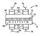
- an assayis performed by adding a solution 60 of different types of “target” analytes 52 - 54 into a cell or container 70 having a plurality of functionalized microbeads 72 - 74 disposed therein.
- the functionalized microbeads 72 - 74 placed in the cell 70have different identification codes 58 that correspond to unique probes 76 - 78 bonded thereto.
- all functionalized microbeads 72 disposed within the cell 70 having an identification code of 12345678is coated with a unique probe 76 .
- All functionalized microbeads 73 disposed within the cell 72 having an identification code of 34128913is coated with a unique probe 77 .
- All functionalized microbeads 77 disposed within the cell 70 having an identification code of 11778154is coated with a unique probe 78 .
- the “target” analytes 52 - 54 within the solution 60are then mixed with the functionalized microbeads 72 - 74 .
- the “target” analytesattach to the complementary probes 76 - 78 , as shown for functionalized microbeads 72 , 73 having codes 12345678 and 34128913. Specifically, as shown in FIG.
- targetanalytes 53 bonded with probes 76 of the functionalized microbeads 72 having the code 12345678, and “target” analytes 52 bonded with probes 77 of the functionalized microbeads 73 having the code 34128913.
- targetanalytes 54 did not bond with any probes, and no “target” analytes 52 - 54 in the solution 60 bonded with probes 78 of the functionalized microbeads 74 having the code 11778154.
- the results of the assaywould show that the unknown “target” analytes in the solution 60 includes “target” analytes 53 , 54 , as will be described in further detail.
- each coded functionalized microbead 72 - 74has a unique probe 76 - 78 , respectively bonded thereto, such as a portion of a single strand of DNA.
- the “target” analytes 52 - 54comprise a plurality of unknown and unique single strands of DNA.
- These “target” analytes 52 - 54are also processed with a fluorescent, such as dyeing, such that the test molecules illuminate.
- the fluorescence of the “target” analytesprovide the means to identify, which functionalized microbeads 72 - 74 have a “target” analyte attached thereto.
- the functionalized microbeads 72 - 74are rinsed off with a saline solution to clean off the uncombined “target” analytes 52 - 54 .
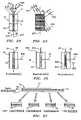
- the functionalized microbeads 72 - 74may be placed in a tray 84 with grooves 82 to allow the functionalized microbeads to be aligned in a predetermined direction, such as that described in U.S. patent application Ser. No. 10/661234, filed contemporaneously, which is incorporated herein by reference.
- the grooves 82may have holes (not shown) that provide suction to keep the functionalized microbeads in position.
- each functionalized microbead 72 - 74is detected for fluorescence and analyzed to determine the identification code 58 of the functionalized microbeads.
- a light source(not shown) may be provided to luminate the microbeads 72 - 74 .
- the bead detector 20determines which “target” analytes 52 - 54 were present in the solution 60 .
- the bead detector 20illuminates the functionalized microbeads 72 - 74 and focuses light 26 reflected by the diffraction grating 12 through a lens 28 onto a CCD array or camera 32 , whereby the code 58 of the functionalized microbead 72 - 74 is determined.
- the bead detector 20includes a fluorescence detector 86 for measuring the fluorescence emanating from “target” analytes 52 - 54 attached to the probes 76 - 78 .
- the fluorescence meter 86includes a lens 88 and optical fiber 90 for receiving and providing the fluorescence from the “target” analyte 52 - 54 to the fluorescence meter.
- the codes in the microbeads 8are detected when illuminated by incident light 24 which produces a diffracted or output light signal 27 to a reader 820 , which includes the optics and electronics necessary to read the codes in each bead 8 , as described herein and/or in the aforementioned copending patent application.
- the reader 820provides a signal on a line 822 indicative of the code in each of the bead 8 .
- the incident light 24may be directed transversely from the side of the tray 84 (or from an end or any other angle) with a narrow band (single wavelength) and/or multiple wavelength source, in which case the code is represented by a spatial distribution of light and/or a wavelength spectrum, respectively, as described hereinafter and in the aforementioned copending patent application.
- a narrow bandsingle wavelength
- multiple wavelength sourcein which case the code is represented by a spatial distribution of light and/or a wavelength spectrum, respectively, as described hereinafter and in the aforementioned copending patent application.
- Other illumination, readout techniques, types of gratings, geometries, materials, etc.may be used for the microbeads 8 , as discussed hereinafter and in the aforementioned patent application.
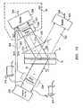
- an optical excitation signal 800is incident on the microbeads 8 through the tray 84 and a fluorescent optical output signal 802 emanates from the beads 8 that have the fluorescent molecule attached.
- the fluorescent optical output signal 802passes through a lens 804 , which provides focused light 806 to a known optical fluorescence detector 808 .
- other imaging opticsmay be used to provide the desired characteristics of the optical image/signal onto the fluorescence detector 808 .
- the detector 808provides an output signal on a line 810 indicative of the amount of fluorescence on a given bead 8 , which can then be interpreted to determine what type of chemical is attached to the bead 10 .
- the tray 84is made of glass or plastic or any material that is transparent to the code reading incident beam 24 and code reading output light beams 27 as well as the fluorescent excitation beam 800 and the output fluorescent optical signal 802 , and is properly suited for the desired application or experiment, e.g., temperature range, harsh chemicals, or other application specific requirements.
- the code signal 822 from the bead code reader 820 and the fluorescent signal 810 from the fluorescence detectorare provided to a known computer 812 .
- the computerreads the code associated with each bead and determines the chemical probe that was attached thereto from a predetermined table that correlates a predetermined relationship between the bead code and the attached probes.
- the computer 812reads the fluorescence associated with each bead and determines the sample or analyte that is attached to the bead from a predetermined table that correlates a predetermined relationship between the fluorescence tag and the analyte attached thereto.
- the computer 812determines information about the analyte and/or the probe as well as about the bonding of the analyte to the probe, and provides such information on a display, printout, storage medium or other interface to an operator, scientist or database for review and/or analysis.
- the sources 801 , 803 the code reader 820 , the fluorescence optics 804 and detector 808 and the computer 812may all be part of an assay reader 824 .
- the reader 24may have only one source beam which provides both the reflected optical signal 27 for determining the code and the fluorescence signal 802 for reading the tagged analyte attached to the beads 8 .
- the input optical signalis a common wavelength that performs both functions simultaneously, or sequentially, if desired.
- the assay of the present inventionmaybe used to carry out any binding assay or screen involving immobilization of one of the binding agents.
- Such solid-phase assays or screensare well known in the chemical and biochemical arts.
- screeningnay involve specific binding of cells to a molecule (e.g. an antibody or antigen) immobilized on a microbead in the assay stick followed by analysis to detect whether or to what extent binding occurs.
- the beadsmay subsequently removed from the assay stick for sorting and analysis via flow cytometry (see e.g. by Needels et al., Proc. Natl. Acad. Sci. USA. Vol. 90, pp. 10700-10704, Nov. 1993).
- biological compounds tatmay be assayed or screened using the assay stick of the present invention include, e.g. agonists and antagonists for cell membrane receptors, toxins, venoms, viral epitopes, hormones, sugars, cofactors, peptides, enzyme substrates, drugs inclusive of opiates and steroids, proteins including antibodies, monoclonal antibodies, antisera reactive with specific antigenic determinants, nucleic acids, lectins, polysacebarides, cellular membranes and organelles.
- the present inventionmay be used in any of a large number of well-known hybridization assays where nucleic acids are immobilized on a surface of a substrate, e.g. genotyping, polymorphism detection, gene expression analysis, fingerprinting, and other methods of DNA- or RNA-based sample analysis or diagnosis.
- spectroscopic methodswell-known in the art may be used to determine directly whether a molecule is bound to a surface coating in a desired configuration.
- Spectroscopic methodsinclude e.g., UV-VIS, NMR,EPR, IR, Raman, mass spectrometry and other methods well-known in the art.
- mass spectrometryalso is now widely employed for the analysis of biological macromolecules. The method typically involves immobilization of a protein on a surface of substrate where it is then exposed to a ligand binding interaction.
- the moleculeis desorbed from the surface and into a spectrometer using a laser (see, e.g. Merchant and Weinberger, “Recent advancements in surface-enhanced laser desorptionlionization-time of flight-mass spectrometry,” Electrophoresis 21: 1164-1177 (2000)).
- the microbeads in the assay of the present inventionmay be used as substrates in the mass spectrometry detection methods described above.
- Various aspects of the present inventionmay be conducted in an automated or semi-automated manner, generally with the assistance of well-known data processing methods.
- Computer programs and other data processing methods well known in the artmay be used to store information including e.g. microbead identifiers, probe sequence information, sample information, and binding signal intensities.
- Data processing methods well known in the artmay be used to read input data covering the desired characteristics.
- the inventionmay be used in many areas such as drug discovery, functionalized substrates, biology, proteomics, combinatorial chemistry, DNA analysis/tracking/sorting/tagging, as well as tagging of molecules, biological particles, matrix support materials, immunoassays, receptor binding assays, scintillation proximity assays, radioactive or non-radioactive proximity assays, and other assays, (including fluorescent, mass spectroscopy), high throughput drug/genome screening, and/or massively parallel assay applications.
- the inventionprovides uniquely identifiable beads with reaction supports by active coatings for reaction tracking to perform multiplexed experiments.
- the inventioncan be used in combinatorial chemistry, active coating and functionalized polymers, as well as immunoassays, and hybridization reactions.
- the inventionenables millions of parallel chemical reactions, enable large-scale repeated chemical reactions, increase productivity and reduce time-to-market for drug and other material development industries.
- a fluorescent labelis probably most convenient, other sorts of labels, e.g., radioactive, enzyme linked, optically detectable, or spectroscopic labels may be used.
- An appropriate detection method applicable to the selected labeling methodcan be selected.
- Suitable labelsinclude radionucleotides, enzymes, substrates, cofactors, inhibitors, magnetic particles, heavy metal atoms, and particularly fluorescers, chemiluminescers, and spectroscopic labels.
- Patents teaching the use of such labelsinclude U.S. Pat. Nos. 3,817,837; 3,850,752; 3,939,350; 3,996,345; 4,277,437; 4,275,149; and 4,366,241.
- the detection system best adapted for high resolution and high sensitivity detectionmay be selected.
- an optically detectable systeme.g., fluorescence or chemilumnescence would be preferred but is not required.
- Other detection systemsmay be adapted to the purpose, e.g., electron microscopy, scanning electron microscopy (SEM), scanning tunneling electron microscopy (STEM), infrared microscopy, atomic force microscopy (AFM), electrical conductance, and image plate transfer.
- the reflected light 27comprises a plurality of beams 26 - 36 that pass through a lens 37 , which provides focused light beams 46 - 56 , respectively, which are imaged onto a CCD camera 60 .
- the lens 37 and the camera 60and any other necessary electronics or optics for performing the functions described herein, make up the reader 29 .
- other imaging opticsmay be used to provide the desired characteristics of the optical image/signal onto the camera 60 (e.g., spots, lines, circles, ovals, etc.), depending on the shape of the substrate 10 and input optical signals.
- a CCD cameraother devices may be used to read/capture the output light.
- the image on the CCD camera 60is a series of illuminated stripes indicating ones and zeros of a digital pattern or code of the grating 12 in the element 8 .
- lines 68 on a graph 70are indicative of a digitized version of the image of FIG. 11 as indicated in spatial periods ( ⁇ 1- ⁇ n).
- Each of the individual spatial periods ( ⁇ 1- ⁇ n) in the grating 12is slightly different, thus producing an array of N unique diffraction conditions (or diffraction angles) discussed more hereinafter.
- the element 8is illuminated from the side, in the region of the grating 12 , at an appropriate input angle, e.g., about 30 degrees, with a single input wavelength ⁇ (monochromatic) source, the diffracted (or reflected) beams 26 - 36 are generated.
- Other input angles ⁇ imay be used if desired, depending on various design parameters as discussed herein and/or in the aforementioned patent application, and provided that a known diffraction equation (Eq.
- Eq. 1is diffraction (or reflection or scatter) relationship between input wavelength ⁇ , input incident angle ⁇ i, output incident angle ⁇ o, and the spatial period ⁇ of the grating 12 .
- mis the “order” of the reflection being observed
- nis the refractive index of the substrate 10 .
- Eq. 1applies to light incident on outer surfaces of the substrate 10 which are parallel to the longitudinal axis of the grating (or the k B vector). Because the angles ⁇ i, ⁇ o are defined outside the substrate 10 and because the effective refractive index of the substrate 10 is substantially a common value, the value of n in Eq. 1 cancels out of this equation.
- the angle ⁇ o of the reflected output lightmay be determined.
- ⁇ osin ⁇ 1 ( ⁇ / ⁇ sin( ⁇ i ))
- the output light 27should fall within an acceptable portion of the Bragg envelope (or normalized reflection efficiency envelope) curve 200 , as indicated by points 204 , 206 , also defined as a Bragg envelope angle ⁇ B, as also discussed herein and/or in the aforementioned patent application.
- the curve 200may be defined as:
- the reflection efficiency I(Eqs. 3 & 4) is maximized, which is at the center or peak of the Bragg envelope.
- the input light angleis referred to as the Bragg angle as is known.
- the efficiencydecreases for other input and output angles (i.e., ⁇ i ⁇ o ), as defined by Eqs. 3 & 4.
- the angle ⁇ i of the input light 24should be set so that the angle ⁇ o of the reflected output light equals the input angle ⁇ i.
- the width of the sin(x)/x functionincreases and, the coefficient to or amplitude of the sinc 2 (or (sin(x)/x) 2 function (and thus the efficiency level across the Bragg envelope) also increases, and vice versa.
- the half-width of the Bragg envelope as well as the efficiency level across the Bragg envelopeboth decrease.
- ⁇ nshould be made as large as possible to maximize the brightness, which allows D to be made smaller.
- ⁇ B⁇ ⁇ ⁇ ⁇ ⁇ ⁇ D ⁇ ⁇ sin ⁇ ( ⁇ i ) Eq. 5
- ⁇is a reflection efficiency factor which is the value for x in the sinc 2 (x) function where the value of sinc 2 (x) has decreased to a predetermined value from the maximum amplitude as indicated by points 204 , 206 on the curve 200 .
- the digital codemay be generated by selectively creating individual index variations (or individual gratings) with the desired spatial periods ⁇ 1- ⁇ n.
- Other illumination, readout techniques, types of gratings, geometries, materials, etc.may be used as discussed in the aforementioned patent application.
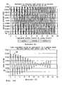
- a sample spectral 17 bit codei.e., 17 different pitches ⁇ 1- ⁇ 17
- CCDCharge Coupled Device
- the length of the substrate 10was 450 microns
- the outer diameter D 1was 65 microns
- the inner diameter Dwas 14 microns
- ⁇ n for the grating 12was about 10 ⁇ 4
- n 1 in portion 20was about 1.458 (at a wavelength of about 1550 nm)
- n 2 in portion 18was about 1.453
- the average pitch spacing ⁇ for the grating 12was about 0.542 microns
- the spacing between pitches ⁇was about 0.36% of the adjacent pitches ⁇ .
- the pitch ⁇ of an individual gratingis the axial spatial period of the sinusoidal variation in the refractive index n 1 in the region 20 of the substrate 10 along the axial length of the grating 12 as indicated by a curve 90 on a graph 91 .
- a sample composite grating 12comprises three individual gratings that are co-located on the substrate 10 , each individual grating having slightly different pitches, ⁇ 1, ⁇ 2, ⁇ 3, respectively, and the difference (or spacing) ⁇ between each pitch ⁇ being about 3.0% of the period of an adjacent pitch ⁇ as indicated by a series of curves 92 on a graph 94 .
- FIG. 14illustration (c), three individual gratings, each having slightly different pitches, ⁇ 1, ⁇ 2, ⁇ 3, respectively, are shown, the difference ⁇ between each pitch ⁇ being about 0.3% of the pitch ⁇ of the adjacent pitch as shown by a series of curves 95 on a graph 97 .
- the individual gratings in FIG. 14 , illustrations (b) and (c)are shown to all start at 0 for illustration purposes; however, it should be understood that, the separate gratings need not all start in phase with each other. Referring to FIG.
- the overlapping of the individual sinusoidal refractive index variation pitches ⁇ 1- ⁇ n in the grating region 20 of the substrate 10produces a combined resultant refractive index variation in the composite grating 12 shown as a curve 96 on a graph 98 representing the combination of the three pitches shown in FIG. 14 , illustration (b).
- the resultant refractive index variation in the grating region 20 of the substrate 10may not be sinusoidal and is a combination of the individual pitches ⁇ (or index variation).
- the maximum number of resolvable bits Nwhich is equal to the number of different grating pitches ⁇ (and hence the number of codes), that can be accurately read (or resolved) using side-illumination and side-reading of the grating 12 in the substrate 10 , is determined by numerous factors, including: the beam width w incident on the substrate (and the corresponding substrate length L and grating length Lg), the thickness or diameter D of the grating 12 , the wavelength ⁇ of incident light, the beam divergence angle ⁇ R , and the width of the Bragg envelope ⁇ B (discussed more in the aforementioned patent application), and may be determined by the equation:
- the bitsmay be read/detected by providing a plurality of wavelengths and reading the wavelength spectrum of the reflected output light signal. In this case, there would be one bit per wavelength, and thus, the code is contained in the wavelength information of the reflected output signal.
- each bit(or ⁇ ) is defined by whether its corresponding wavelength falls within the Bragg envelope, not by its angular position within the Bragg envelope 200 .
- itis not limited by the number of angles that can fit in the Bragg envelope 200 for a given composite grating 12 , as in the embodiment discussed hereinbefore.
- the only limitation in the number of bits Nis the maximum number of grating pitches ⁇ that can be superimposed and optically distinguished in wavelength space for the output beam.
- the reflection wavelength spectrum ( ⁇ 1- ⁇ n) of the reflected output beam 310will exhibit a series of reflection peaks 695 , each appearing at the same output Bragg angle ⁇ o.
- Each wavelength peak 695 ( ⁇ 1- ⁇ n)corresponds to an associated spatial period ( ⁇ 1- ⁇ n), which make up the grating 12 .
- One way to measure the bits in wavelength spaceis to have the input light angle ⁇ i equal to the output light angle ⁇ o, which is kept at a constant value, and to provide an input wavelength ⁇ that satisfies the diffraction condition (Eq. 1) for each grating pitch ⁇ . This will maximize the optical power of the output signal for each pitch ⁇ detected in the grating 12 .
- the transmission wavelength spectrum of the transmitted output beam 330(which is transmitted straight through the grating 12 ) will exhibit a series of notches (or dark spots) 696 .
- the transmitted light 330may be detected at the detector/reader 308 . It should be understood that the optical signal levels for the reflection peaks 695 and transmission notches 696 will depend on the “strength” of the grating 12 , i.e., the magnitude of the index variation n in the grating 12 .
- the bitsmay be detected by continuously scanning the input wavelength.
- a known optical source 300provides the input light signal 24 of a coherent scanned wavelength input light shown as a graph 304 .
- the source 300provides a sync signal on a line 306 to a known reader 308 .
- the sync signalmay be a timed pulse or a voltage ramped signal, which is indicative of the wavelength being provided as the input light 24 to the substrate 10 at any given time.
- the reader 308may be a photodiode, CCD camera, or other optical detection device that detects when an optical signal is present and provides an output signal on a line 309 indicative of the code in the substrate 10 or of the wavelengths present in the output light, which is directly related to the code, as discussed herein.
- the grating 12reflects the input light 24 and provides an output light signal 310 to the reader 308 .
- the wavelength of the input signalis set such that the reflected output light 310 through an optical lens 321 will be substantially in the center 314 of the Bragg envelope 200 for the individual grating pitch (or bit) being read.
- the source 300may provide a continuous broadband wavelength input signal such as that shown as a graph 316 .
- the reflected output beam 310 signalis provided to a narrow band scanning filter 318 which scans across the desired range of wavelengths and provides a filtered output optical signal 320 through an optical lens 321 to the reader 308 .
- the filter 318provides a sync signal on a line 322 to the reader, which is indicative of which wavelengths are being provided on the output signal 320 to the reader and may be similar to the sync signal discussed hereinbefore on the line 306 from the source 300 .
- the source 300does not need to provide a sync signal because the input optical signal 24 is continuous.
- the scanning filtermay be located in the path of the input beam 24 as indicated by the dashed box 324 , which provides the sync signal on a line 323 .
- the reader 308may be a known optical spectrometer (such as a known spectrum analyzer), capable of measuring the wavelength of the output light.
- each readout wavelengthis associated with a predetermined number of bits within the Bragg envelope. Bits (or grating pitches ⁇ ) written for different wavelengths do not show up unless the correct wavelength is used.
- the bitscan be read using one wavelength and many angles, many wavelengths and one angle, or many wavelengths and many angles.
- the grating 12may have a thickness or depth D which is comparable or smaller than the incident beam wavelength ⁇ .
- Thisis known as a “thin” diffraction grating (or the full angle Bragg envelope is 180 degrees).
- the half-angle Bragg envelope ⁇ Bis substantially 90 degrees; however, ⁇ n must be made large enough to provide sufficient reflection efficiency, per Eqs. 3 and 4.
- D* ⁇ n ⁇ /2which corresponds to a ⁇ phase shift between adjacent minimum and maximum refractive index values of the grating 12 .
- phase shift between adjacent minimum and maximum refractive index values of the grating 12should approach a ⁇ phase shift; however, other phase shifts may be used.
- the grating 12is illuminated with the input light 24 oriented on a line 705 orthogonal to the longitudinal grating vector 703 .
- the +/ ⁇ 1 st order beamscorresponds to output beams 700 , 702 , respectively.
- the +/ ⁇ 2 nd order beamscorresponds to output beams 704 , 706 , respectively.
- the 0 th order (undiffracted) beamcorresponds to beam 708 and passes straight through the substrate.
- the output beams 700 - 708project spectral spots or peaks 710 - 718 , respectively, along a common plane, shown from the side by a line 709 , which is parallel to the upper surface of the substrate 10 .
- one can use only the +/ ⁇ 1 st order (m+/ ⁇ 1) output beams for the code, in which case there would be only 2 peaks to detect, 712 , 714 .
- an individual peakmay be used instead of using a pair of output peaks for a given order.
- the +/ ⁇ 1 st order beamscorresponds to output beams 720 , 722 , respectively.
- the output beams 720 - 726 corresponding to the second pitch ⁇ 2project spectral spots or peaks 730 - 736 , respectively, which are at a different location than the point 710 - 716 , but along the same common plane, shown from the side by the line 709 .
- each different pitchcorresponds to a different elevation or output angle which corresponds to a predetermined set of spectral peaks. Accordingly, the presence or absence of a particular peak or set of spectral peaks defines the code.
- the readout anglesmay no longer be symmetric, leading to possible difficulties in readout.
- the angular sensitivity to the alignment of the longitudinal axis of the substrate 10 to the input angle ⁇ i of incident radiationis reduced or eliminated.
- the input lightcan be oriented along substantially any angle ⁇ i with respect to the grating 12 without causing output signal degradation, due the large Bragg angle envelope.
- the grating 12can be oriented at any rotational (or azimuthal) angle without causing output signal degradation.
- changing the incident angle ⁇ iwill affect the output angle ⁇ o of the reflected light in a predetermined predictable way, thereby allowing for accurate output code signal detection or compensation.
- the bitscan also be multiplexed in an azimuthal (or rotational) angle ⁇ a of the substrate.
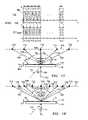
- a plurality of gratings 750 , 752 , 754 , 756 each having the same pitch ⁇are disposed in a surface 701 of the substrate 10 and located in the plane of the substrate surface 701 .
- the input light 24is incident on all the gratings 750 , 752 , 754 , 756 simultaneously.
- Each of the gratingsprovides output beams oriented based on the grating orientation.
- the grating 750provides the output beams 764 , 762
- the grating 752provides the output beams 766 , 768
- the grating 754provides the output beams 770 , 772
- the grating 756provides the output beams 774 , 776 .
- Each of the output beamsprovides spectral peaks or spots (similar to that discussed hereinbefore), which are located in a plane 760 that is parallel to the substrate surface plane 701 .
- a single grating pitch ⁇can produce many bits depending on the number of gratings that can be placed at different azimuthal (rotational) angles on the surface of the substrate 10 and the number of output beam spectral peaks that can be spatially and optically resolved/detected.
- Each bitmay be viewed as the presence or absence of a pair of peaks located at a predetermined location in space in the plane 760 .
- the azimuthal multiplexingcan be combined with the elevation or output angle multiplexing discussed hereinbefore to provide two levels of multiplexing. Accordingly, for a thin grating, the number of bits can be multiplexed based on the number of grating pitches ⁇ and/or geometrically by the orientation of the grating pitches.
- the edges of the substrate 10no longer scatter light from the incident angle into the “code angular space”, as discussed herein and/or in the aforementioned patent application.
- a continuous broadband wavelength sourcemay be used as the optical source if desired.
- the pitches ⁇ in the grating 12may be created at a angle ⁇ g.
- the pitcheswhen the input light 24 is incident normal to the surface 792 , will produce a reflected output beam 790 having an angle ⁇ o determined by Eq. 1 as adjusted for the blaze angle ⁇ g. This can provide another level of multiplexing bits in the code.
- an additional level of multiplexingmay be provided by having the optical code use other numerical bases, if intensity levels of each bit are used to indicate code information. This could be achieved by having a corresponding magnitude (or strength) of the refractive index change ( ⁇ n) for each grating pitch ⁇ .
- Four intensity rangesare shown for each bit number or pitch ⁇ , providing for a Base-4 code (where each bit corresponds to 0,1,2, or 3). The lowest intensity level, corresponding to a 0, would exist when this pitch A is not present in the grating 12 . The next intensity level 450 would occur when a first low level ⁇ n1 exists in the grating that provides an output signal within the intensity range corresponding to a 1.
- the next intensity level 452would occur when a second higher level ⁇ n2 exists in the grating 12 that provides an output signal within the intensity range corresponding to a 2.
- the next intensity level 454would occur when a third higher level 6 n 3 exists in the grating 12 that provides an output signal within the intensity range corresponding to a 3.
- the input light 24may be incident on the substrate 10 on an end face 600 of the substrate 10 .
- the input light 24will be incident on the grating 12 having a more significant component of the light (as compared to side illumination discussed hereinbefore) along the longitudinal grating axis 207 of the grating (along the grating vector k B ), as shown by a line 602 .
- the light 602reflects off the grating 12 as indicated by a line 604 and exits the substrate as output light 608 .
- the code informationis readable only in the spectral wavelength of the reflected beam, similar to that discussed hereinbefore for wavelength based code reading.
- the input signalin this case may be a scanned wavelength source or a broadband wavelength source.
- the code informationmay be obtained in reflection from the reflected beam 614 or in transmission by the transmitted beam 616 that passes through the grating 12 .
- n inis the refractive index of the first (input) medium
- n outis the refractive index of the second (output) medium
- ⁇ in and ⁇ outare measured from a line 620 normal to an incident surface 622 .
- the grating region 20 of the substrate 10will act as a known optical waveguide for certain wavelengths.
- the grating region 20acts as a “core” along which light is guided and the outer region 18 acts as a “cladding” which helps confine or guide the light.
- such a waveguidewill have a known “numerical aperture” ( ⁇ na) that will allow light 630 that is within the aperture ⁇ na to be directed or guided along the grating axis 207 and reflected axially off the grating 12 and returned and guided along the waveguide.
- the grating 12will reflect light having the appropriate wavelengths equal to the pitches ⁇ present in the grating 12 back along the region 20 (or core) of the waveguide, and pass the remaining wavelengths of light as the light 632 .
- having the grating region 20 act as an optical waveguide for wavelengths reflected by the grating 12allows incident light that is not aligned exactly with the grating axis 207 to be guided along and aligned with the grating 12 axis 207 for optimal grating reflection.
- any standard waveguidemay be used, e.g., a standard telecommunication single mode optical fiber (125 micron diameter or 80 micron diameter fiber with about a 8-10 micron diameter), or a larger diameter waveguide (greater than 0.5 mm diameter), such as is describe in U.S. patent application, Ser. No. 09/455,868, filed Dec. 6, 1999, entitled “Large Diameter Waveguide, Grating”.
- any type of optical waveguidemay be used for the optical substrate 10 , such as, a multi-mode, birefringent, polarization maintaining, polarizing, multi-core, multi-cladding, or microsturctured optical waveguide, or a flat or planar waveguide (where the waveguide is rectangular shaped), or other waveguides.
- the substrate 10does not behave as a waveguide for the incident or reflected light and the incident light 24 will be diffracted (or reflected) as indicated by lines 642 , and the codes detected as discussed hereinbefore for the end-incidence condition discussed hereinbefore with FIG. 45 , and the remaining light 640 passes straight through.
- illustration (b)alternatively, the input light 24 may be incident from the side and, if the grating 12 has the appropriate blaze angle, the reflected light will exit from the end face 652 as indicated by a line 654 .
- the grating 12may have a plurality of different pitch angles 660 , 662 , which reflect the input light 24 to different output angles as indicated by lines 664 , 666 . This provides another level of multiplexing (spatially) additional codes, if desired.
- the grating 12may be impressed in the substrate 10 by any technique for writing, impressed, embedded, imprinted, or otherwise forming a diffraction grating in the volume of or on a surface of a substrate 10 .
- Examples of some known techniquesare described in U.S. Pat. Nos. 4,725,110 and 4,807,950, entitled “Method for Impressing Gratings Within Fiber Optics”, to Glenn et al; and U.S. Pat. No. 5,388,173, entitled “Method and Apparatus for Forming Aperiodic Gratings in Optical Fibers”, to Glenn, respectively, and U.S. Pat. No.
- the grating 12may be partially or totally created by etching or otherwise altering the outer surface geometry of the substrate to create a corrugated or varying surface geometry of the substrate, such as is described in U.S. Pat. No. 3,891,302, entitled “Method of Filtering Modes in Optical Waveguides”, to Dabby et al, which is incorporated herein by reference to the extent necessary to understand the present invention, provided the resultant optical refractive profile for the desired code is created.
- the grating 12may be made by depositing dielectric layers onto the substrate, similar to the way a known thin film filter is created, so as to create the desired resultant optical refractive profile for the desired code.
- the substrate 10(and/or the element 8 ) may have end-view cross-sectional shapes other than circular, such as square, rectangular, elliptical, clam-shell, D-shaped, or other shapes, and may have side-view sectional shapes other than rectangular, such as circular, square, elliptical, clam-shell, D-shaped, or other shapes.
- 3D geometries other than a cylindermay be used, such as a sphere, a cube, a pyramid or any other 3D shape.
- the substrate 10may have a geometry that is a combination of one or more of the foregoing shapes.
- the shape of the element 8 and the size of the incident beammay be made to minimize any end scatter off the end face(s) of the element 8 , as is discussed herein and/or in the aforementioned patent application. Accordingly, to minimize such scatter, the incident beam 24 may be oval shaped where the narrow portion of the oval is smaller than the diameter D 1 , and the long portion of the oval is smaller than the length L of the element 8 . Alternatively, the shape of the end faces may be rounded or other shapes or may be coated with an antireflective coating.
- any given dimension for the region 20 of the grating 12may be less than any corresponding dimension of the substrate 10 .
- the grating 12may be embedded within or part of a much larger substrate 12 .
- the element 8may be embedded or formed in or on a larger object for identification of the object.
- the dimensions, geometries, materials, and material properties of the substrate 10are selected such that the desired optical and material properties are met for a given application.
- the resolution and range for the optical codesare scalable by controlling these parameters as discussed herein and/or in the aforementioned patent application.
- the substrate 10may have an outer coating 799 , such as a polymer or other material that may be dissimilar to the material of the substrate 10 , provided that the coating 799 on at least a portion of the substrate, allows sufficient light to pass through the substrate for adequate optical detection of the code.
- the coating 799may be on any one or more sides of the substrate 10 .
- the coating 799may be a material that causes the element 8 to float or sink in certain fluids (liquid and/or gas) solutions.
- the substrate 10may be made of a material that is less dense than certain fluid (liquids and/or gas) solutions, thereby allowing the elements 8 to float or be buoyant or partially buoyant.
- the substratemay be made of a porous material, such as controlled pore glass (CPG) or other porous material, which may also reduce the density of the element 8 and may make the element 8 buoyant or partially-buoyant in certain fluids.
- CPGcontrolled pore glass
- the grating 12is axially spatially invariant.
- the substrate 10 with the grating 12may be axially subdivided or cut into many separate smaller substrates 30 - 36 and each substrate 30 - 36 will contain the same code as the longer substrate 21 had before it was cut.
- the limit on the size of the smaller substrates 30 - 36is based on design and performance factors discussed herein and/or in the aforementioned patent application.
- one purpose of the outer region 18 (or region without the grating 12 ) of the substrate 10is to provide mechanical or structural support for the inner grating region 20 .
- the entire substrate 10may comprise the grating 12 , if desired.
- the support portionmay be completely or partially beneath, above, or along one or more sides of the grating region 20 , such as in a planar geometry, or a D-shaped geometry, or other geometries, as described herein and/or in the aforementioned patent application.
- the non-grating portion 18 of the substrate 10may be used for other purposes as well, such as optical lensing effects or other effects (discussed herein or in the aforementioned patent application).
- the end faces of the substrate 10need not be perpendicular to the sides or parallel to each other. However, for applications where the elements 8 are stacked end-to-end, the packing density may be optimized if the end faces are perpendicular to the sides.
- two or more substrates 10 , 250may be attached together to form the element 8 , e.g., by an adhesive, fusing or other attachment techniques.
- the gratings 12 , 252may have the same or different codes.
- the substrate 10may have multiple regions 80 , 90 and one or more of these regions may have gratings in them.
- the substrate 10may have multiple regions 80 , 90 and one or more of these regions may have gratings in them.
- the length L of the element 8may be shorter than its diameter D, thus, having a geometry such as a plug, puck, wafer, disc or plate.
- the substrate 10may have a plurality of the gratings 12 having the same codes written therein at numerous different angular or rotational (or azimuthal) positions of the substrate 10 .
- two gratings 550 , 552having axial grating axes 551 , 553 , respectively may have a common central (or pivot or rotational) point where the two axes 551 , 553 intersect.
- the angle ⁇ i of the incident light 24is aligned properly with the grating 550 and is not aligned with the grating 552 , such that output light 555 is reflected off the grating 550 and light 557 passes through the grating 550 as discussed herein. If the element 8 is rotated as shown by the arrows 559 , the angle ⁇ i of incident light 24 will become aligned properly with the grating 552 and not aligned with the grating 550 such that output light 555 is reflected off the grating 552 and light 557 passes through the grating 552 .
- the beadWhen multiple gratings are located in this rotational orientation, the bead may be rotated as indicated by a line 559 and there may be many angular positions that will provide correct (or optimal) incident input angles ⁇ i to the grating. While this example shows a circular cross-section, this technique may be used with any shape cross-section.
- illustrations (a), (b), (c), (d), and (e) the substrate 10may have one or more holes located within the substrate 10 .
- holes 560may be located at various points along all or a portion of the length of the substrate 10 . The holes need not pass all the way through the substrate 10 . Any number, size and spacing for the holes 560 may be used if desired.
- holes 572may be located very close together to form a honeycomb-like area of all or a portion of the cross-section.
- one (or more) inner hole 566may be located in the center of the substrate 10 or anywhere inside of where the grating region(s) 20 are located.
- the inner hole 566may be coated with a reflective coating 573 to reflect light to facilitate reading of one or more of the gratings 12 and/or to reflect light diffracted off one or more of the gratings 12 .
- the incident light 24may reflect off the grating 12 in the region 20 and then reflect off the surface 573 to provide output light 577 .
- the incident light 24may reflect off the surface 573 , then reflect off the grating 12 and provide the output light 575 .
- the grating region 20may run axially or circumferentially 571 around the substrate 10 .
- the holes 579may be located circumferentially around the grating region 20 or transversely across the substrate 10 .
- the grating 12may be located circumferentially around the outside of the substrate 10 , and there may be holes 574 inside the substrate 10 . In that case, the incident light 24 reflects off the grating 12 to provide the optical light 576 .
- the substrate 10may have one or more protruding portions or teeth 570 , 578 , 580 extending radially and/or circumferentially from the substrate 10 .
- the teeth 570 , 578 , 580may have any other desired shape.
- the grating region 20may have end cross-sectional shapes other than circular and may have side cross-sectional shapes other than rectangular, such as any of the geometries described herein for the substrate 10 .
- the grating region 20may have a oval cross-sectional shape as shown by dashed lines 581 , which may be oriented in a desired direction, consistent with the teachings herein. Any other geometries for the substrate 10 or the grating region 20 may be used if desired, as described herein.
- At least a portion of a side of the substrate 10may be coated with a reflective coating 514 to allow incident light 510 to be reflected back to the same side from which the incident light came, as indicated by reflected light 512 .
- the substrate 10can be electrically and/or magnetically polarized, by a dopant or coating, which may be used to ease handling and/or alignment or orientation of the substrate 10 and/or the grating 12 , or used for other purposes.
- the beadmay be coated with conductive material, e.g., metal coating on the inside of a holey substrate, or metallic dopant inside the substrate. In these cases, such materials can cause the substrate 10 to align in an electric or magnetic field.
- the substratecan be doped with an element or compound that fluoresces or glows under appropriate illumination, e.g., a rare earth dopant, such as Erbium, or other rare earth dopant or fluorescent or luminescent molecule.
- a rare earth dopantsuch as Erbium, or other rare earth dopant or fluorescent or luminescent molecule.
- fluorescence or luminescencemay aid in locating and/or aligning substrates.
Landscapes
- Chemical & Material Sciences (AREA)
- Health & Medical Sciences (AREA)
- Hematology (AREA)
- Analytical Chemistry (AREA)
- General Health & Medical Sciences (AREA)
- Physics & Mathematics (AREA)
- Clinical Laboratory Science (AREA)
- Chemical Kinetics & Catalysis (AREA)
- General Physics & Mathematics (AREA)
- Fluid Mechanics (AREA)
- Dispersion Chemistry (AREA)
- Investigating, Analyzing Materials By Fluorescence Or Luminescence (AREA)
- Diffracting Gratings Or Hologram Optical Elements (AREA)
Abstract
Description
sin(θi)+sin(θo)=mλ/nΛ Eq. 1
where Eq. 1 is diffraction (or reflection or scatter) relationship between input wavelength λ, input incident angle θi, output incident angle θo, and the spatial period Λ of the grating12. Further, m is the “order” of the reflection being observed, and n is the refractive index of the
θo=sin−1(λ/Λ−sin(θi)) Eq. 2
For example, for an input wavelength λ=532 nm, a grating spacing Λ=0.532 microns (or 532 nm), and an input angle of incidence θi=30 degrees, the output angle of reflection will be θo=30 degrees. Alternatively, for an input wavelength λ=632 nm, a grating spacing Λ=0.532 microns (or 532 nm), and an input angle θi of 30 degrees, the output angle of reflection θo will be at 43.47 degrees, or for an input angle θi=37 degrees, the output angle of reflection will be θo=37 degrees. Any input angle that satisfies the design requirements discussed herein and/or in the aforementioned patent application may be used.
where K=2πδn/λ, where, δn is the local refractive index modulation amplitude of the grating and λ is the input wavelength, sinc(x)=sin(x)/x, and the vectors ki=2πcos(θi)/λ and ko=2πcos (θo)/λ are the projections of the incident light and the output (or reflected) light, respectively, onto the
where η is a reflection efficiency factor which is the value for x in the sinc2(x) function where the value of sinc2(x) has decreased to a predetermined value from the maximum amplitude as indicated by
λ=Λ[sin(θo)+sin(θi)] Eq. 7
λ=2 neffΛ Eq. 8
where neffis the effective index of refraction of the substrate, λ is the input (and output wavelength) and Λ is the pitch. This relation, as is known, may be derived from Eq. 1 where θi=θo=90 degrees.
ninsin θin=noutsin θout Eq. 9
Claims (136)
Priority Applications (12)
| Application Number | Priority Date | Filing Date | Title |
|---|---|---|---|
| US10/661,031US7349158B2 (en) | 2002-09-12 | 2003-09-12 | Diffraction grating-based encoded micro-particles for multiplexed experiments |
| PCT/US2004/001685WO2004066210A1 (en) | 2003-01-22 | 2004-01-22 | Hybrid random bead/chip based microarray |
| US10/763,995US7164533B2 (en) | 2003-01-22 | 2004-01-22 | Hybrid random bead/chip based microarray |
| PCT/US2004/030038WO2005029047A2 (en) | 2003-09-12 | 2004-09-13 | Diffraction grating-based encoded microparticle assay stick |
| US11/206,987US20060057729A1 (en) | 2003-09-12 | 2005-08-18 | Diffraction grating-based encoded element having a substance disposed thereon |
| US11/226,914US7901630B2 (en) | 2002-08-20 | 2005-09-13 | Diffraction grating-based encoded microparticle assay stick |
| US11/544,309US7923260B2 (en) | 2002-08-20 | 2006-10-06 | Method of reading encoded particles |
| US11/546,027US7872804B2 (en) | 2002-08-20 | 2006-10-10 | Encoded particle having a grating with variations in the refractive index |
| US11/607,837US7659983B2 (en) | 2003-01-22 | 2006-11-30 | Hybrid random bead/chip based microarray |
| US12/644,255US7843567B2 (en) | 2003-01-22 | 2009-12-22 | Methods of identifying an analyte and nucleic acid analysis |
| US12/876,927US8614852B2 (en) | 2002-08-20 | 2010-09-07 | Elongated microparticles having an optically detectable code configured to at least one of reflect or filter light |
| US12/941,568US8049893B2 (en) | 2003-01-22 | 2010-11-08 | Methods of identifying analytes and using encoded particles |
Applications Claiming Priority (5)
| Application Number | Priority Date | Filing Date | Title |
|---|---|---|---|
| US41054102P | 2002-09-12 | 2002-09-12 | |
| US64568903A | 2003-08-20 | 2003-08-20 | |
| US10/645,686US20040075907A1 (en) | 2002-08-20 | 2003-08-20 | Diffraction grating-based encoded micro-particles for multiplexed experiments |
| PCT/US2003/029244WO2004025563A1 (en) | 2002-09-12 | 2003-09-12 | Diffraction grating-based encoded micro-particles for multiplexed experiments |
| US10/661,031US7349158B2 (en) | 2002-09-12 | 2003-09-12 | Diffraction grating-based encoded micro-particles for multiplexed experiments |
Related Parent Applications (2)
| Application Number | Title | Priority Date | Filing Date |
|---|---|---|---|
| US10/645,686Continuation-In-PartUS20040075907A1 (en) | 2002-08-20 | 2003-08-20 | Diffraction grating-based encoded micro-particles for multiplexed experiments |
| US10/661,836Continuation-In-PartUS7399643B2 (en) | 2002-08-20 | 2003-09-12 | Method and apparatus for aligning microbeads in order to interrogate the same |
Related Child Applications (8)
| Application Number | Title | Priority Date | Filing Date |
|---|---|---|---|
| US64568903AContinuation-In-Part | 2002-08-20 | 2003-08-20 | |
| US10/661,234Continuation-In-PartUS7106513B2 (en) | 2002-08-20 | 2003-09-12 | Diffraction grating-based encoded particle |
| US10/763,995Continuation-In-PartUS7164533B2 (en) | 2002-08-20 | 2004-01-22 | Hybrid random bead/chip based microarray |
| US10/990,057Continuation-In-PartUS20050227252A1 (en) | 2002-08-20 | 2004-11-15 | Diffraction grating-based encoded articles for multiplexed experiments |
| US11/206,987Continuation-In-PartUS20060057729A1 (en) | 2003-09-12 | 2005-08-18 | Diffraction grating-based encoded element having a substance disposed thereon |
| US11/226,914Continuation-In-PartUS7901630B2 (en) | 2002-08-20 | 2005-09-13 | Diffraction grating-based encoded microparticle assay stick |
| US11/544,309Continuation-In-PartUS7923260B2 (en) | 2002-08-20 | 2006-10-06 | Method of reading encoded particles |
| US11/546,027Continuation-In-PartUS7872804B2 (en) | 2002-08-20 | 2006-10-10 | Encoded particle having a grating with variations in the refractive index |
Publications (2)
| Publication Number | Publication Date |
|---|---|
| US20040125424A1 US20040125424A1 (en) | 2004-07-01 |
| US7349158B2true US7349158B2 (en) | 2008-03-25 |
Family
ID=39960159
Family Applications (1)
| Application Number | Title | Priority Date | Filing Date |
|---|---|---|---|
| US10/661,031Expired - Fee RelatedUS7349158B2 (en) | 2002-08-20 | 2003-09-12 | Diffraction grating-based encoded micro-particles for multiplexed experiments |
Country Status (5)
| Country | Link |
|---|---|
| US (1) | US7349158B2 (en) |
| EP (1) | EP1540591A1 (en) |
| AU (1) | AU2003270726A1 (en) |
| CA (1) | CA2499046A1 (en) |
| WO (1) | WO2004025563A1 (en) |
Cited By (29)
| Publication number | Priority date | Publication date | Assignee | Title |
|---|---|---|---|---|
| US20050227252A1 (en)* | 2002-08-20 | 2005-10-13 | Moon John A | Diffraction grating-based encoded articles for multiplexed experiments |
| US20060063271A1 (en)* | 2002-09-12 | 2006-03-23 | Putnam Martin A | Method and apparatus for aligning microbeads in order to interrogate the same |
| US20060072177A1 (en)* | 2002-08-20 | 2006-04-06 | Putnam Martin A | Diffraction grating-based encoded microparticle assay stick |
| US20060118630A1 (en)* | 2004-11-16 | 2006-06-08 | Illumina, Inc. | Holographically encoded elements for microarray and other tagging labeling applications, and method and apparatus for making and reading the same |
| US20060119913A1 (en)* | 2003-08-20 | 2006-06-08 | Illumina, Inc. | Fourier scattering methods for encoding microbeads and methods and apparatus for reading the same |
| US20080085565A1 (en)* | 2002-08-20 | 2008-04-10 | Cyvera Corporation | Method of reading encoded particles |
| US20080129990A1 (en)* | 2003-01-22 | 2008-06-05 | Cyvera Corporation | Hybrid random bead/chip based microarray |
| US20080286814A1 (en)* | 2006-12-04 | 2008-11-20 | Perkinelmer Las, Inc. | Biomarkers for Detecting Cancer |
| US20090034078A1 (en)* | 2004-02-19 | 2009-02-05 | Illumina, Inc. | Optical identification element having a non-waveguide substrate |
| US20090073520A1 (en)* | 2004-11-17 | 2009-03-19 | Illumina, Inc. | Encoded microparticles and a method for fabricating |
| US20090194589A1 (en)* | 2002-08-20 | 2009-08-06 | Illumina, Inc. | Optical reader system for substrates having an optically readable code |
| US7623624B2 (en) | 2005-11-22 | 2009-11-24 | Illumina, Inc. | Method and apparatus for labeling using optical identification elements characterized by X-ray diffraction |
| US20100246005A1 (en)* | 2002-08-20 | 2010-09-30 | Cyvera Corporation | Encoded particle having a grating with variations in the refractive index |
| US7898735B2 (en) | 2002-09-12 | 2011-03-01 | Illumina, Inc. | Methods and systems for writing an optical code within or on a fiber substrate |
| US20110105361A1 (en)* | 2009-10-30 | 2011-05-05 | Illumina, Inc. | Microvessels, microparticles, and methods of manufacturing and using the same |
| US8498052B2 (en) | 2002-08-20 | 2013-07-30 | Illumina, Inc. | Composition including an item and an encoded optical substrate and a method for identifying an item |
| US9216412B2 (en) | 2009-11-23 | 2015-12-22 | Cyvek, Inc. | Microfluidic devices and methods of manufacture and use |
| US9229001B2 (en) | 2009-11-23 | 2016-01-05 | Cyvek, Inc. | Method and apparatus for performing assays |
| US9500645B2 (en) | 2009-11-23 | 2016-11-22 | Cyvek, Inc. | Micro-tube particles for microfluidic assays and methods of manufacture |
| US9546932B2 (en) | 2009-11-23 | 2017-01-17 | Cyvek, Inc. | Microfluidic assay operating system and methods of use |
| US9651568B2 (en) | 2009-11-23 | 2017-05-16 | Cyvek, Inc. | Methods and systems for epi-fluorescent monitoring and scanning for microfluidic assays |
| US9700889B2 (en) | 2009-11-23 | 2017-07-11 | Cyvek, Inc. | Methods and systems for manufacture of microarray assay systems, conducting microfluidic assays, and monitoring and scanning to obtain microfluidic assay results |
| US9759718B2 (en) | 2009-11-23 | 2017-09-12 | Cyvek, Inc. | PDMS membrane-confined nucleic acid and antibody/antigen-functionalized microlength tube capture elements, and systems employing them, and methods of their use |
| US9855735B2 (en) | 2009-11-23 | 2018-01-02 | Cyvek, Inc. | Portable microfluidic assay devices and methods of manufacture and use |
| US10065403B2 (en) | 2009-11-23 | 2018-09-04 | Cyvek, Inc. | Microfluidic assay assemblies and methods of manufacture |
| US20180313743A1 (en)* | 2017-04-28 | 2018-11-01 | Becton, Dickinson And Company | Particle detection cartridges, systems thereof and methods for using the same |
| US10228367B2 (en) | 2015-12-01 | 2019-03-12 | ProteinSimple | Segmented multi-use automated assay cartridge |
| US10482361B2 (en) | 2015-07-05 | 2019-11-19 | Thewhollysee Ltd. | Optical identification and characterization system and tags |
| US20220136043A1 (en)* | 2019-03-01 | 2022-05-05 | Revere Biosensors, Llc | Systems and methods for separating decoded arrays |
Families Citing this family (62)
| Publication number | Priority date | Publication date | Assignee | Title |
|---|---|---|---|---|
| US7349158B2 (en) | 2002-09-12 | 2008-03-25 | Cyvera Corporation | Diffraction grating-based encoded micro-particles for multiplexed experiments |
| US7441703B2 (en) | 2002-08-20 | 2008-10-28 | Illumina, Inc. | Optical reader for diffraction grating-based encoded optical identification elements |
| AU2003267192A1 (en) | 2002-09-12 | 2004-04-30 | Cyvera Corporation | Method and apparatus for aligning elongated microbeads in order to interrogate the same |
| WO2005033681A1 (en)* | 2003-10-01 | 2005-04-14 | Cyvera Corporation | Optical reader for diffraction grating-based encoded optical identification elements |
| WO2005082110A2 (en)* | 2004-02-26 | 2005-09-09 | Illumina Inc. | Haplotype markers for diagnosing susceptibility to immunological conditions |
| GB2412730B (en)* | 2004-03-31 | 2006-08-23 | Toshiba Res Europ Ltd | An encoded carrier and a method of monitoring a carrier |
| WO2006055735A2 (en) | 2004-11-16 | 2006-05-26 | Illumina, Inc | Scanner having spatial light modulator |
| WO2006058334A2 (en)* | 2004-11-29 | 2006-06-01 | Perkinelmer Life And Analytical Sciences | Prticle-based multiplex assay for identifying glycosylation |
| GB0426809D0 (en)* | 2004-12-07 | 2005-01-12 | Univ Southampton | Nano-optical diffraction bar-code tagging for biological and chemical applications |
| US7871770B2 (en) | 2005-08-09 | 2011-01-18 | Maxwell Sensors, Inc. | Light transmitted assay beads |
| US8232092B2 (en) | 2005-08-09 | 2012-07-31 | Maxwell Sensors, Inc. | Apparatus and method for digital magnetic beads analysis |
| US7858307B2 (en) | 2005-08-09 | 2010-12-28 | Maxwell Sensors, Inc. | Light transmitted assay beads |
| EP2485052B1 (en)* | 2005-09-13 | 2015-05-06 | Affymetrix, Inc. | Encoded microparticles |
| US8178278B2 (en)* | 2005-09-13 | 2012-05-15 | Affymetrix, Inc. | Miniaturized microparticles |
| US7803751B2 (en)* | 2005-12-09 | 2010-09-28 | Illumina, Inc. | Compositions and methods for detecting phosphomonoester |
| US20070166739A1 (en) | 2005-12-23 | 2007-07-19 | Perkinelmer Las, Inc. | Comparative genomic hybridization on encoded multiplex particles |
| WO2007075910A2 (en)* | 2005-12-23 | 2007-07-05 | Perkinelmer Las, Inc. | Methods and compositions for detecting enzymatic activity |
| US7932037B2 (en)* | 2007-12-05 | 2011-04-26 | Perkinelmer Health Sciences, Inc. | DNA assays using amplicon probes on encoded particles |
| US20100009373A1 (en)* | 2005-12-23 | 2010-01-14 | Perkinelmer Health Sciences, Inc. | Methods and compositions relating to multiplex genomic gain and loss assays |
| US20070166835A1 (en)* | 2005-12-23 | 2007-07-19 | Perkinelmer Las, Inc. | Multiplex assays using magnetic and non-magnetic particles |
| US20090104613A1 (en)* | 2005-12-23 | 2009-04-23 | Perkinelmer Las, Inc. | Methods and compositions relating to multiplexed genomic gain and loss assays |
| US7830575B2 (en) | 2006-04-10 | 2010-11-09 | Illumina, Inc. | Optical scanner with improved scan time |
| US7550271B2 (en)* | 2006-04-28 | 2009-06-23 | Perkinelmer Las, Inc. | Detecting phospho-transfer activity |
| WO2008064016A2 (en)* | 2006-11-13 | 2008-05-29 | Perkinelmer Las, Inc. | Detecting molecular interactions |
| US20080242560A1 (en)* | 2006-11-21 | 2008-10-02 | Gunderson Kevin L | Methods for generating amplified nucleic acid arrays |
| US20080241831A1 (en)* | 2007-03-28 | 2008-10-02 | Jian-Bing Fan | Methods for detecting small RNA species |
| US20080279874A1 (en)* | 2007-05-07 | 2008-11-13 | Wyeth | Compositions and methods for modulation of plk1 kinase activity |
| EP2617837A3 (en) | 2007-06-08 | 2013-10-23 | Biogen Idec MA Inc. | Biomarkers for predicting anti-TNF responsiveness or non-responsiveness |
| EP2179289A1 (en)* | 2007-08-08 | 2010-04-28 | Maxwell Sensors, Inc. | Apparatus and method for digital magnetic beads analysis |
| US20110046009A1 (en)* | 2009-08-24 | 2011-02-24 | Perkinelmer Health Sciences, Inc. | Methods for detecting dna methylation using encoded particles |
| WO2011038360A1 (en) | 2009-09-25 | 2011-03-31 | Signature Genomics Laboratories Llc | Multiplex (+/-) stranded arrays and assays for detecting chromosomal abnormalities associated with cancer and other diseases |
| WO2011100503A1 (en) | 2010-02-11 | 2011-08-18 | Dana Farber Cancer Institute, Inc. | Methods for predicting likelihood of responding to treatment |
| US9566560B2 (en) | 2011-10-06 | 2017-02-14 | Illumina, Inc. | Array domains having rotated patterns |
| CN102980844B (en)* | 2012-12-10 | 2014-09-17 | 同济大学 | Method for detecting washed surface of optical substrate used for laser thin film element |
| WO2016156575A2 (en) | 2015-04-02 | 2016-10-06 | Hmnc Value Gmbh | Genetic predictors of a response to treatment with crhr1 antagonists |
| EP3277836B1 (en) | 2015-04-02 | 2019-02-27 | HMNC Value GmbH | Method of treatment using genetic predictors of a response to treatment with ssr-125543 |
| CA3050852C (en) | 2017-01-20 | 2021-03-09 | Omniome, Inc. | Genotyping by polymerase binding |
| CA3050241C (en) | 2017-01-20 | 2022-11-29 | Omniome, Inc. | Allele-specific capture of nucleic acids |
| GB201701686D0 (en) | 2017-02-01 | 2017-03-15 | Illunina Inc | System & method with fiducials having offset layouts |
| GB201701689D0 (en) | 2017-02-01 | 2017-03-15 | Illumia Inc | System and method with fiducials of non-closed shapes |
| GB201701688D0 (en) | 2017-02-01 | 2017-03-15 | Illumia Inc | System and method with fiducials in non-recliner layouts |
| GB201701691D0 (en)* | 2017-02-01 | 2017-03-15 | Illumina Inc | System and method with reflective fiducials |
| SG11201906442TA (en) | 2017-02-01 | 2019-08-27 | Illumina Inc | System and method with fiducials responding to multiple excitation frequencies |
| WO2018152162A1 (en) | 2017-02-15 | 2018-08-23 | Omniome, Inc. | Distinguishing sequences by detecting polymerase dissociation |
| US10161003B2 (en) | 2017-04-25 | 2018-12-25 | Omniome, Inc. | Methods and apparatus that increase sequencing-by-binding efficiency |
| WO2019046288A1 (en) | 2017-08-31 | 2019-03-07 | Massachusetts Institute Of Technology | Compositions and multiplex assays for characterizing active proteases and their inhibitors |
| US10400272B1 (en) | 2018-04-26 | 2019-09-03 | Omniome, Inc. | Methods and compositions for stabilizing nucleic acid-nucleotide-polymerase complexes |
| AU2019276719A1 (en) | 2018-05-31 | 2020-11-26 | Pacific Biosciences Of California, Inc. | Increased signal to noise in nucleic acid sequencing |
| CA3107165A1 (en) | 2018-07-24 | 2020-01-30 | Omniome, Inc. | Serial formation of ternary complex species |
| WO2020060811A1 (en) | 2018-09-17 | 2020-03-26 | Omniome, Inc. | Engineered polymerases for improved sequencing |
| CN113166805B (en) | 2018-12-04 | 2024-07-16 | 加利福尼亚太平洋生物科学股份有限公司 | Mixed-phase fluids for nucleic acid sequencing and other analytical assays |
| US11499189B2 (en) | 2019-02-14 | 2022-11-15 | Pacific Biosciences Of California, Inc. | Mitigating adverse impacts of detection systems on nucleic acids and other biological analytes |
| US11377655B2 (en) | 2019-07-16 | 2022-07-05 | Pacific Biosciences Of California, Inc. | Synthetic nucleic acids having non-natural structures |
| EP4265628A3 (en) | 2019-09-10 | 2024-01-03 | Pacific Biosciences of California, Inc. | Reversible modification of nucleotides |
| EP4045683B1 (en) | 2019-10-18 | 2025-02-19 | Pacific Biosciences of California, Inc. | Methods for capping nucleic acids |
| WO2021092431A1 (en) | 2019-11-08 | 2021-05-14 | Omniome, Inc. | Engineered polymerases for improved sequencing by binding |
| CN115243792A (en) | 2020-02-04 | 2022-10-25 | 加利福尼亚太平洋生物科学股份有限公司 | Flow cell and methods of making and using the same |
| EP4114966B1 (en) | 2020-03-03 | 2025-02-26 | Pacific Biosciences Of California, Inc. | Methods and compositions for sequencing double stranded nucleic acids |
| EP4459285A3 (en) | 2020-04-14 | 2025-01-22 | (INSERM) Institut National de la Santé et de la Recherche Médicale | Methods for detecting the presence of coronavirus-specific antibodies in a subject |
| US20230183798A1 (en) | 2020-05-05 | 2023-06-15 | Pacific Biosciences Of California, Inc. | Compositions and methods for modifying polymerase-nucleic acid complexes |
| WO2022043415A1 (en) | 2020-08-27 | 2022-03-03 | INSERM (Institut National de la Santé et de la Recherche Médicale) | Methods for detecting the presence of pemphigus-specific autoantibodies in a sample |
| WO2025010160A1 (en) | 2023-07-06 | 2025-01-09 | Pacific Biosciences Of California, Inc. | Methods and compositions for stabilizing concatemers |
Citations (355)
| Publication number | Priority date | Publication date | Assignee | Title |
|---|---|---|---|---|
| US3891302A (en) | 1973-09-28 | 1975-06-24 | Western Electric Co | Method of filtering modes in optical waveguides |
| DE2416652A1 (en) | 1974-04-05 | 1975-10-16 | Dierk Dr Flasdieck | Data card or carrier - is made from base material with indicators added using electrolytic or galvanic processes |
| US3916182A (en) | 1972-08-21 | 1975-10-28 | Western Electric Co | Periodic dielectric waveguide filter |
| US3968476A (en) | 1974-07-17 | 1976-07-06 | Sperry Rand Corporation | Spurious signal removal in optical processor fingerprint identification apparatus |
| US4011435A (en) | 1974-02-01 | 1977-03-08 | Ncr Corporation | Optical indicia marking and detection system |
| US4023010A (en) | 1975-09-08 | 1977-05-10 | Ncr Corporation | Optical identification system and reader for reading optical gratings on a record medium |
| US4053228A (en) | 1975-12-12 | 1977-10-11 | Michael Schiller | Finger identification |
| US4053433A (en) | 1975-02-19 | 1977-10-11 | Minnesota Mining And Manufacturing Company | Method of tagging with color-coded microparticles |
| US4131337A (en) | 1976-02-18 | 1978-12-26 | Hoechst Aktiengesellschaft | Comparison reader for holographic identification cards |
| US4168146A (en) | 1975-01-27 | 1979-09-18 | Ab Kabi | Immunoassay with test strip having antibodies bound thereto |
| US4301139A (en) | 1979-06-21 | 1981-11-17 | Ames-Yissum Ltd. | Multilayer column chromatography specific binding assay method, test device and test kit |
| US4386274A (en) | 1980-11-10 | 1983-05-31 | Saul Altshuler | Isotope separation by standing waves |
| US4400616A (en) | 1980-08-21 | 1983-08-23 | International Business Machines Corporation | Document card containing information in holographic form |
| US4445229A (en) | 1980-03-12 | 1984-04-24 | U.S. Philips Corporation | Device for adjusting a movable electro-acoustic sound transducer |
| US4447546A (en) | 1982-08-23 | 1984-05-08 | Myron J. Block | Fluorescent immunoassay employing optical fiber in capillary tube |
| GB2118189B (en) | 1982-02-26 | 1985-05-15 | Shimadzu Corp | An automatic synthesizer for dna |
| US4537504A (en)* | 1981-02-03 | 1985-08-27 | Lgz Landis & Gyr Zug Ag | Security blank with enhanced authenticating features, and a method and an apparatus for determining the genuineness of the security blank |
| US4560881A (en) | 1984-03-13 | 1985-12-24 | Syntex (U.S.A.) Inc. | Method and apparatus for enhanced detection of electromagnetic signals |
| US4562157A (en) | 1983-05-25 | 1985-12-31 | National Research Development Corporation | Diagnostic device incorporating a biochemical ligand |
| GB2129551B (en) | 1982-04-28 | 1986-02-26 | Mochida Pharm Co Ltd | Immunoassay vessel conveying analysis information |
| US4647544A (en) | 1984-06-25 | 1987-03-03 | Nicoli David F | Immunoassay using optical interference detection |
| GB2138821B (en) | 1983-04-19 | 1987-04-01 | California Inst Of Techn | Apparatus and process for the synthesis of chemical compounds |
| US4678752A (en) | 1985-11-18 | 1987-07-07 | Becton, Dickinson And Company | Automatic random access analyzer |
| US4685480A (en) | 1985-08-30 | 1987-08-11 | Abbott Laboratories | Combined washer and aspirator |
| US4690907A (en) | 1983-12-19 | 1987-09-01 | Daiichi Pure Chemicals Co., Ltd. | Capillary tube immunoassay |
| US4701754A (en) | 1985-04-18 | 1987-10-20 | Fmc Corporation | Indicator device for substance receiving wells in a microtiter plate |
| US4716121A (en) | 1985-09-09 | 1987-12-29 | Ord, Inc. | Fluorescent assays, including immunoassays, with feature of flowing sample |
| US4725110A (en) | 1984-08-13 | 1988-02-16 | United Technologies Corporation | Method for impressing gratings within fiber optics |
| US4740468A (en) | 1985-02-14 | 1988-04-26 | Syntex (U.S.A.) Inc. | Concentrating immunochemical test device and method |
| US4740688A (en) | 1986-03-20 | 1988-04-26 | Smiths Industries Public Limited Company | Optical transducers with wavelength coding |
| US4748110A (en) | 1985-09-25 | 1988-05-31 | Abbott Laboratories | Immunoassay for HTLV-III antigens |
| US4762420A (en) | 1986-04-01 | 1988-08-09 | Fisons Plc | Photometric reading device for serological analysis |
| US4767719A (en) | 1986-05-20 | 1988-08-30 | Amersham International Plc | Assay apparatus having piezoelectric slab generating effective diffraction grating in applied analyte-specific film |
| US4816659A (en) | 1987-10-13 | 1989-03-28 | Control Module Inc. | Bar code reader head |
| US4841140A (en) | 1987-11-09 | 1989-06-20 | Honeywell Inc. | Real-time color comparator |
| US4877747A (en) | 1985-04-12 | 1989-10-31 | Plessey Overseas Limited | Optical assay: method and apparatus |
| US4880752A (en) | 1984-09-21 | 1989-11-14 | Ciba Corning Diagnostics Corp. | Dielectric waveguide sensors and their use in immunoassays |
| US4882288A (en) | 1984-09-14 | 1989-11-21 | North John R | Assay technique and equipment |
| US4921805A (en) | 1987-07-29 | 1990-05-01 | Life Technologies, Inc. | Nucleic acid capture method |
| US4931384A (en) | 1982-12-21 | 1990-06-05 | Ares-Serono N.V. | Optical assay technique |
| US4937048A (en) | 1983-01-31 | 1990-06-26 | Olympus Optical Company Limited | Carrier transporting apparatus and carrier container for use in an immunological analysis |
| US4958376A (en) | 1985-12-27 | 1990-09-18 | Grumman Aerospace Corporation | Robotic vision, optical correlation system |
| US4992385A (en) | 1986-07-24 | 1991-02-12 | Ares-Serono Research And Development Limited Partnership | Polymer-coated optical structures and methods of making and using the same |
| US5003600A (en) | 1989-08-03 | 1991-03-26 | The United States Of America As Represented By The Department Of Energy | Diffraction gratings used as identifying markers |
| USRE33581E (en) | 1984-06-25 | 1991-04-30 | Immunoassay using optical interference detection | |
| WO1991006496A1 (en) | 1989-10-30 | 1991-05-16 | Autotrol Corporation | Pellet dispenser |
| US5030558A (en) | 1986-11-07 | 1991-07-09 | Syntex (U.S.A.) Inc. | Qualitative immunochromatographic method and device |
| US5033826A (en) | 1989-03-27 | 1991-07-23 | Hewlett-Packard Company | High temporal resolution optical instrument |
| US5065008A (en) | 1989-10-18 | 1991-11-12 | Fuji Photo Film Co., Ltd. | Scanning microscope and scanning mechanism for the same |
| US5067155A (en) | 1990-05-09 | 1991-11-19 | Control Module Inc. | Method and means to limit access to computer systems |
| US5081012A (en) | 1988-03-29 | 1992-01-14 | Applied Research Systems Ars Holding N.V. | Waveguide sensor with input and reflecting gratings and its use in immunoassay |
| US5089387A (en) | 1988-07-07 | 1992-02-18 | Adeza Biomedical Corporation | Dna probe diffraction assay and reagents |
| US5090807A (en) | 1990-01-10 | 1992-02-25 | Environmental Research Institute Of Michigan | Real time optical pre-detection processing of multispectral image data |
| US5095194A (en) | 1989-10-12 | 1992-03-10 | Joseph Barbanell | Holographic credit card with automatical authentication and verification |
| US5100238A (en) | 1987-06-11 | 1992-03-31 | Orlon Corporation Limited | Cuvette and apparatus for performing biological assays |
| US5104209A (en) | 1991-02-19 | 1992-04-14 | Her Majesty The Queen In Right Of Canada, As Represented By The Minister Of Communications | Method of creating an index grating in an optical fiber and a mode converter using the index grating |
| US5115121A (en) | 1990-01-05 | 1992-05-19 | Control Module Inc. | Variable-sweep bar code reader |
| US5129974A (en) | 1990-08-23 | 1992-07-14 | Colorcode Unlimited Corporation | Microlabelling system and method of making thin labels |
| US5138468A (en) | 1990-02-02 | 1992-08-11 | Dz Company | Keyless holographic lock |
| US5141848A (en) | 1987-01-21 | 1992-08-25 | Abbott Laboratories | Confirmatory immunoassay using microparticle separation |
| US5144461A (en) | 1991-06-20 | 1992-09-01 | Horan Philip R | Portable holographic recording apparatus |
| US5160701A (en) | 1986-02-18 | 1992-11-03 | Abbott Laboratories | Solid-phase analytical device and method for using same |
| US5166813A (en) | 1988-05-31 | 1992-11-24 | Nygene Corporation | Optical evaluation using a hologram barrier filter |
| US5192980A (en) | 1990-06-27 | 1993-03-09 | A. E. Dixon | Apparatus and method for method for spatially- and spectrally-resolved measurements |
| US5196350A (en) | 1991-05-29 | 1993-03-23 | Omnigene, Inc. | Ligand assay using interference modulation |
| US5200794A (en) | 1989-08-11 | 1993-04-06 | Nhk Spring Co., Ltd. | Optical head for an optical authenticity identifing system |
| WO1993009668A1 (en) | 1991-11-22 | 1993-05-27 | Affymax Technology N.V. | Combinatorial strategies for polymer synthesis |
| US5218594A (en) | 1990-03-08 | 1993-06-08 | Pioneer Electric Corporation | Recording medium with an optical waveguide and player for playing the same |
| US5283777A (en) | 1991-04-26 | 1994-02-01 | Pioneer Electronic Corporation | Three-dimensional optical recording medium and optical information recording apparatus using the same |
| US5291027A (en) | 1992-07-08 | 1994-03-01 | Toppan Printing Co., Ltd. | Optical identification multiple diffraction grating mark member and card using the same |
| US5291006A (en) | 1989-08-11 | 1994-03-01 | Nhk Spring Co., Ltd. | Authenticity identifying system for information storage cards |
| US5300764A (en) | 1991-09-11 | 1994-04-05 | Nhk Spring Company, Ltd. | Transparent optical identification label with infrared directivity |
| US5307332A (en) | 1972-08-25 | 1994-04-26 | Thomson-Csf | Optical disk arrangement with diffractive tracks and a photoelectric assembly providing positional control information |
| US5310686A (en) | 1987-03-10 | 1994-05-10 | Ares Serono Research & Development Limited Partnership | Polymer-coated optical structures |
| US5342790A (en) | 1992-10-30 | 1994-08-30 | Becton Dickinson And Company | Apparatus for indirect fluorescent assay of blood samples |
| US5349442A (en) | 1991-09-20 | 1994-09-20 | Eg&G Idaho, Inc. | Hand held phase-shifting diffraction moire interferometer |
| US5352582A (en) | 1993-10-28 | 1994-10-04 | Hewlett-Packard Company | Holographic based bio-assay |
| US5364797A (en) | 1993-05-20 | 1994-11-15 | Mobil Oil Corp. | Sensor device containing mesoporous crystalline material |
| US5367588A (en) | 1992-10-29 | 1994-11-22 | Her Majesty The Queen In Right Of Canada, As Represented By The Minister Of Communications | Method of fabricating Bragg gratings using a silica glass phase grating mask and mask used by same |
| WO1994028119A1 (en) | 1993-05-21 | 1994-12-08 | Smithkline Beecham P.L.C. | Novel process and apparatus |
| US5372783A (en) | 1992-08-03 | 1994-12-13 | Sapidyne, Inc. | Assay system |
| US5374816A (en) | 1991-12-19 | 1994-12-20 | Bianco; James S. | Optical method and apparatus for authenticating degaussed magnetic identification means |
| US5374818A (en) | 1992-03-09 | 1994-12-20 | Control Module Inc. | Identification means with integral memory device |
| US5388173A (en) | 1993-12-20 | 1995-02-07 | United Technologies Corporation | Method and apparatus for forming aperiodic gratings in optical fibers |
| US5395558A (en) | 1991-12-06 | 1995-03-07 | Johnson & Johnson Vision Products, Inc. | Method of making a soft ophthalmic lens |
| US5426297A (en) | 1993-09-27 | 1995-06-20 | United Technologies Corporation | Multiplexed Bragg grating sensors |
| US5442433A (en) | 1989-08-11 | 1995-08-15 | Nhk Spring Co., Ltd. | Identification system for an article having individually attached patches |
| US5448659A (en) | 1993-02-01 | 1995-09-05 | Matsushita Electric Industrial Co., Ltd. | Waveguide-type image transmission device and fingerprint identification device |
| US5451528A (en) | 1992-03-27 | 1995-09-19 | Abbott Laboratories | Methods for providing homogeneous reagents |
| US5455178A (en) | 1990-05-03 | 1995-10-03 | Hoffmann-La Roche Inc. | Microoptical sensor and method |
| US5461475A (en) | 1994-02-02 | 1995-10-24 | Physical Optics Corporation | Binary optical spectrum analyzer |
| US5465176A (en) | 1991-12-19 | 1995-11-07 | Control Module Inc. | Method of embossing repeating patterns on a substrate, the patterns having different rates of repetition |
| US5468649A (en) | 1994-02-15 | 1995-11-21 | Abbott Laboratories | Process for labeling acridinium to microparticles and application in an instrument |
| US5506674A (en) | 1992-05-01 | 1996-04-09 | Sumitomo Electric Industries, Ltd. | Method for identifying an optical fiber using a pattern of reflected light |
| US5514785A (en) | 1990-05-11 | 1996-05-07 | Becton Dickinson And Company | Solid supports for nucleic acid hybridization assays |
| US5528045A (en) | 1995-04-06 | 1996-06-18 | Becton Dickinson And Company | Particle analyzer with spatially split wavelength filter |
| WO1996024061A1 (en) | 1995-02-02 | 1996-08-08 | Ontogen Corporation | Methods and apparatus for synthesizing labeled combinatorial chemical libraries |
| US5547849A (en) | 1993-02-17 | 1996-08-20 | Biometric Imaging, Inc. | Apparatus and method for volumetric capillary cytometry |
| US5559613A (en) | 1993-08-09 | 1996-09-24 | France Telecom Etablissement Autonome De Droit Public | Photorefractive device with quantum wells |
| EP0395300B1 (en) | 1989-04-28 | 1996-10-02 | Westaim Technologies Inc. | Thin film diagnostic device |
| WO1996036436A1 (en) | 1995-04-25 | 1996-11-21 | Irori | Remotely programmable matrices with memories and uses thereof |
| US5585639A (en) | 1995-07-27 | 1996-12-17 | Hewlett-Packard Company | Optical scanning apparatus |
| US5587832A (en) | 1993-10-20 | 1996-12-24 | Biophysica Technologies, Inc. | Spatially light modulated confocal microscope and method |
| US5607188A (en) | 1994-06-24 | 1997-03-04 | Imation Corp. | Marking of optical disc for customized identification |
| US5610287A (en) | 1993-12-06 | 1997-03-11 | Molecular Tool, Inc. | Method for immobilizing nucleic acid molecules |
| US5621515A (en) | 1994-01-25 | 1997-04-15 | Nhk Spring Co., Ltd. | Identification system using regions of predetermined properties interspersed among regions of other properties |
| US5624850A (en) | 1994-06-06 | 1997-04-29 | Idetek, Inc. | Immunoassays in capillaries |
| US5625472A (en) | 1992-12-23 | 1997-04-29 | Lucent Technologies Inc. | Method for forming distributed Bragg reflectors in optical media |
| WO1997015690A1 (en) | 1995-10-24 | 1997-05-01 | Curagen Corporation | Method and apparatus for identifying, classifying, or quantifying dna sequences in a sample without sequencing |
| US5627663A (en) | 1993-08-31 | 1997-05-06 | Control Module Inc. | Secure optical identification method and means |
| US5627040A (en) | 1991-08-28 | 1997-05-06 | Becton Dickinson And Company | Flow cytometric method for autoclustering cells |
| WO1997017258A1 (en) | 1995-11-09 | 1997-05-15 | Glaxo Group Limited | Device and methods for dispensing beads |
| US5633724A (en) | 1995-08-29 | 1997-05-27 | Hewlett-Packard Company | Evanescent scanning of biochemical array |
| US5633975A (en) | 1995-11-14 | 1997-05-27 | The United States Of America As Represented By The Administrator Of The National Aeronautics And Space Administration | Security system responsive to optical fiber having Bragg grating |
| WO1997012680A3 (en) | 1995-10-03 | 1997-08-21 | Irori | Matrices with memories, sensors with memories and uses thereof |
| WO1997031282A1 (en) | 1996-02-22 | 1997-08-28 | Isis Innovation Limited | Confocal microscope |
| US5663790A (en) | 1993-04-08 | 1997-09-02 | Pharmacia Biosensor Ab | Method and apparatus for determination of refractive index |
| US5667976A (en) | 1990-05-11 | 1997-09-16 | Becton Dickinson And Company | Solid supports for nucleic acid hybridization assays |
| GB2306484B (en) | 1995-10-26 | 1997-09-24 | Univ Hertfordshire | Coded particles for process sequence tracking in combinatorial compound library preparation |
| EP0798573A1 (en) | 1995-10-16 | 1997-10-01 | Sumitomo Electric Industries, Ltd. | Optical fiber diffraction grating, production method thereof and laser light source |
| US5712912A (en) | 1995-07-28 | 1998-01-27 | Mytec Technologies Inc. | Method and apparatus for securely handling a personal identification number or cryptographic key using biometric techniques |
| US5721435A (en) | 1996-04-09 | 1998-02-24 | Hewlett Packard Company | Methods and apparatus for measuring optical properties of biological and chemical substances |
| WO1997034171A3 (en) | 1996-02-28 | 1998-02-26 | Kenneth C Johnson | Microlens scanner for microlithography and wide-field confocal microscopy |
| US5729365A (en) | 1996-01-11 | 1998-03-17 | Sandia Corporation | Computer generated holographic microtags |
| US5736330A (en) | 1995-10-11 | 1998-04-07 | Luminex Corporation | Method and compositions for flow cytometric determination of DNA sequences |
| US5742432A (en) | 1991-12-19 | 1998-04-21 | Bianco; James S. | Apparatus for manufacture of diffraction gratings for identification means |
| US5745617A (en) | 1996-12-30 | 1998-04-28 | D-Star Technologies, Llc | Near-ultra-violet formation of refractive-index grating using reflective phase mask |
| US5745615A (en) | 1996-10-11 | 1998-04-28 | Lucent Technologies Inc. | Method of making an optical fiber grating, and article made by the method |
| EP0723149A3 (en) | 1995-01-19 | 1998-05-06 | Hitachi, Ltd. | Capillary array electrophoresis system |
| US5760961A (en) | 1995-03-16 | 1998-06-02 | Landis & Gyr Technology Innovation Ag | Optical information carrier having diffractive features and diffraction modulation layers |
| US5759778A (en) | 1993-08-10 | 1998-06-02 | Life Technologies, Inc. | Method of nucleic acid sequence selection |
| WO1998024549A1 (en) | 1996-12-04 | 1998-06-11 | Smithkline Beecham Plc | Device for transfer and separation of microbeads |
| US5766956A (en) | 1997-05-27 | 1998-06-16 | American Research Corporation | Diode laser-based chemical and biological sensor |
| US5771251A (en) | 1994-05-06 | 1998-06-23 | University Of Southampton | Optical fibre distributed feedback laser |
| US5776694A (en) | 1990-10-19 | 1998-07-07 | Becton Dickinson Company | Diagnostic kits useful for selectively detecting microorganisms in samples |
| US5793502A (en) | 1993-08-31 | 1998-08-11 | Bianco; James S. | Secure optical identification means and method with enhanced variability |
| US5798273A (en) | 1996-09-25 | 1998-08-25 | Becton Dickinson And Company | Direct read lateral flow assay for small analytes |
| US5799231A (en) | 1996-07-25 | 1998-08-25 | International Business Machines Corporation | Variable index distributed mirror |
| US5801857A (en) | 1989-09-28 | 1998-09-01 | Gao Gesellschaft Fur Automation Und Organisation Mbh | Data carrier having an optically variable element and methods for producing it |
| US5804384A (en) | 1996-12-06 | 1998-09-08 | Vysis, Inc. | Devices and methods for detecting multiple analytes in samples |
| US5812272A (en) | 1997-01-30 | 1998-09-22 | Hewlett-Packard Company | Apparatus and method with tiled light source array for integrated assay sensing |
| WO1998044740A1 (en) | 1997-03-31 | 1998-10-08 | Iterated Systems, Inc. | System and method for compressing data using differential coding of coefficient addresses |
| US5822472A (en) | 1994-05-27 | 1998-10-13 | Novartis Corporation | Process for detecting evanescently excited luminescence |
| US5824557A (en) | 1996-04-02 | 1998-10-20 | Panvera Corporation | Method for detecting and quantitating nucleic acid impurities in biochemical preparations |
| US5824478A (en) | 1996-04-30 | 1998-10-20 | Vysis, Inc. | Diagnostic methods and probes |
| US5830622A (en) | 1994-02-14 | 1998-11-03 | The University Of Sydney | Optical grating |
| US5831698A (en) | 1996-08-20 | 1998-11-03 | International Business Machines Corporation | Electrically variable diffuser |
| US5837475A (en) | 1997-01-30 | 1998-11-17 | Hewlett-Packard Co. | Apparatus and method for scanning a chemical array |
| US5837552A (en) | 1991-07-22 | 1998-11-17 | Medifor, Ltd. | Surface-enhanced analytical procedures and substrates |
| US5846737A (en) | 1996-07-26 | 1998-12-08 | Molecular Probes, Inc. | Conjugates of sulforhodamine fluorophores with enhanced fluorescence |
| WO1999002266A1 (en) | 1997-07-11 | 1999-01-21 | Akzo Nobel N.V. | A device for performing an assay, a method for manufacturing said device, and use of a membrane in the manufacture of said device |
| US5874187A (en) | 1996-08-15 | 1999-02-23 | Lucent Technologies Incorporated | Photo recording medium |
| US5881197A (en) | 1997-02-14 | 1999-03-09 | University Of Southampton | Optical fibre and optical fibre device |
| US5895750A (en) | 1984-05-10 | 1999-04-20 | Abbott Laboratories | Immunoassay for the detection of ligands |
| GB2299235B (en) | 1995-03-20 | 1999-04-21 | Rainer Uhl | Arrangement for confocal fluorescence microscopy |
| EP0911667A1 (en) | 1997-10-22 | 1999-04-28 | Max-Planck-Gesellschaft zur Förderung der Wissenschaften e.V. | Programmable spatially light modulated microscope and microscopy method |
| WO1999009042A3 (en) | 1997-08-13 | 1999-05-06 | Cepheid | Microstructures for the manipulation of fluid samples |
| EP0916981A1 (en) | 1997-11-17 | 1999-05-19 | Max-Planck-Gesellschaft zur Förderung der Wissenschaften e.V. | Confocal spectroscopy system and method |
| WO1999032654A1 (en) | 1997-12-22 | 1999-07-01 | Hitachi Chemical Co., Ltd. | Direct rt-pcr on oligonucleotide-immobilized pcr microplates |
| US5922550A (en) | 1996-12-18 | 1999-07-13 | Kimberly-Clark Worldwide, Inc. | Biosensing devices which produce diffraction images |
| US5922617A (en) | 1997-11-12 | 1999-07-13 | Functional Genetics, Inc. | Rapid screening assay methods and devices |
| US5925878A (en) | 1997-08-20 | 1999-07-20 | Imation Corp. | Diffraction anomaly sensor having grating coated with protective dielectric layer |
| US5925562A (en) | 1995-04-25 | 1999-07-20 | Irori | Remotely programmable matrices with memories |
| WO1999042209A1 (en) | 1998-02-23 | 1999-08-26 | Takeda Chemical Industries, Ltd. | Apparatus and method for separating and supplying single beads from a group of beads for use in combinatorial synthesis process |
| US5972542A (en) | 1996-12-30 | 1999-10-26 | D-Star Technologies, Inc. | Method of making a phase mask and mask for use in near-ultra-violet formation of refractive-index grating |
| US5976896A (en) | 1994-06-06 | 1999-11-02 | Idexx Laboratories, Inc. | Immunoassays in capillary tubes |
| US5981166A (en) | 1997-04-23 | 1999-11-09 | Pharmaseq, Inc. | Screening of soluble chemical compounds for their pharmacological properties utilizing transponders |
| US5986838A (en) | 1995-02-14 | 1999-11-16 | Iomega Corporation | Thin retroreflective marker for data storage cartridge |
| US5989923A (en) | 1994-03-28 | 1999-11-23 | Btg International Limited | Hologram containing sensor |
| US5998796A (en) | 1997-12-22 | 1999-12-07 | Spectrumedix Corporation | Detector having a transmission grating beam splitter for multi-wavelength sample analysis |
| US6001510A (en) | 1994-08-15 | 1999-12-14 | Meng; Wu | Method for producing laser hologram anti-counterfeit mark with identifying card and inspecting card and inspecting apparatus for the mark |
| US6005691A (en)* | 1996-12-11 | 1999-12-21 | Hewlett-Packard Company | High-security machine-readable holographic card |
| EP0972817A1 (en) | 1998-07-13 | 2000-01-19 | Dai Nippon Printing Co., Ltd. | Ferroelectric charge-transport liquid crystal material |
| US6017754A (en) | 1995-08-24 | 2000-01-25 | Invitrogen Corporation | System for isolating and identifying eukaryotic cells transfected with genes and vectors, host cells and methods thereof |
| JP2000035521A (en) | 1998-05-07 | 2000-02-02 | Nippon Telegr & Teleph Corp <Ntt> | Optical fiber |
| US6025129A (en) | 1995-04-25 | 2000-02-15 | Irori | Remotely programmable matrices with memories and uses thereof |
| US6025283A (en) | 1995-05-12 | 2000-02-15 | The Real Gold Card Company Limited | Charge card |
| US6027694A (en) | 1996-10-17 | 2000-02-22 | Texperts, Inc. | Spillproof microplate assembly |
| US6030581A (en) | 1997-02-28 | 2000-02-29 | Burstein Laboratories | Laboratory in a disk |
| US6035082A (en) | 1998-03-16 | 2000-03-07 | Luna Innovations, Inc. | Process for preparing an optical fiber sensor with enhanced sensitivity |
| US6036807A (en) | 1995-12-12 | 2000-03-14 | Ing Groep Nv | Method for applying a security code to an article |
| US6043880A (en) | 1997-09-15 | 2000-03-28 | Becton Dickinson And Company | Automated optical reader for nucleic acid assays |
| WO2000016893A2 (en) | 1998-09-17 | 2000-03-30 | Smartbead Technologies Limited | Bio-assay technique |
| US6046925A (en) | 1997-04-14 | 2000-04-04 | The Regents Of The University Of California | Photochromic fluorescent proteins and optical memory storage devices based on fluorescent proteins |
| US6049727A (en) | 1996-07-08 | 2000-04-11 | Animas Corporation | Implantable sensor and system for in vivo measurement and control of fluid constituent levels |
| US6060256A (en) | 1997-12-16 | 2000-05-09 | Kimberly-Clark Worldwide, Inc. | Optical diffraction biosensor |
| US6067167A (en) | 1998-08-10 | 2000-05-23 | Innovative Lasers Corp. | ILS sensors for drug detection within vehicles |
| WO2000008443A9 (en) | 1998-08-08 | 2000-05-25 | Imp Cancer Res Tech | Multiple frequency fluorescence lifetime imaging |
| US6078048A (en) | 1998-04-27 | 2000-06-20 | The Regents Of The University Of California | Immersion echelle spectrograph |
| US6084995A (en) | 1997-12-19 | 2000-07-04 | Nortel Networks Corporation | Reducing scanning errors |
| US6097485A (en) | 1999-03-08 | 2000-08-01 | Integrated Waveguides, Inc. | Microchip optical transport technology for use in a personal flow cytometer |
| US6096496A (en) | 1997-06-19 | 2000-08-01 | Frankel; Robert D. | Supports incorporating vertical cavity emitting lasers and tracking apparatus for use in combinatorial synthesis |
| US6096596A (en) | 1995-01-20 | 2000-08-01 | Micron Technology Inc. | Very high-density DRAM cell structure and method for fabricating it |
| US6103535A (en) | 1996-05-31 | 2000-08-15 | University Of Maryland | Optical fiber evanescent field excited fluorosensor and method of manufacture |
| WO2000061198A1 (en) | 1999-04-12 | 2000-10-19 | Hitachi Chemical Co., Ltd. | Method of producing probe arrays for biological materials using fine particles |
| US6137931A (en) | 1997-05-01 | 2000-10-24 | Sumitomo Electric Industries, Ltd. | Method for determining a condition of aging for optical fiber grating |
| US6143247A (en) | 1996-12-20 | 2000-11-07 | Gamera Bioscience Inc. | Affinity binding-based system for detecting particulates in a fluid |
| WO2000037969A3 (en) | 1998-12-04 | 2000-11-16 | Cidra Corp | Compression-tuned bragg grating and laser |
| US6156501A (en) | 1993-10-26 | 2000-12-05 | Affymetrix, Inc. | Arrays of modified nucleic acid probes and methods of use |
| US6160656A (en) | 1998-01-07 | 2000-12-12 | Templex Technology, Inc. | Method and apparatus for optical correlation recognition by time-integrated nonlinear detection |
| US6160240A (en) | 1997-10-14 | 2000-12-12 | Biotronik Mess-und Therapiegerate GmbH & Co Ingenieurburo Berlin | Method of producing microstructural medical implants |
| US6159748A (en) | 1995-03-13 | 2000-12-12 | Affinitech, Ltd | Evaluation of autoimmune diseases using a multiple parameter latex bead suspension and flow cytometry |
| US6164548A (en) | 1998-02-05 | 2000-12-26 | Safecard Id System, Inc. | Methods of creating a tamper resistant informational article |
| US6165592A (en) | 1992-11-18 | 2000-12-26 | Oesterreichische Nationalbank | Document with doped optical security attribute, layer composite for making same and test device for testing the document for authenticity |
| US6174648B1 (en) | 1997-07-08 | 2001-01-16 | Oki Electric Industry Co., Ltd. | Optical filter fabrication method using fiber holder with spiral groove and phase mask with spiral diffraction grating |
| GB2319838B (en) | 1996-10-31 | 2001-01-17 | Hewlett Packard Co | Producing a chemical array |
| US6194563B1 (en) | 1999-03-26 | 2001-02-27 | Vysis, Inc. | Solid phase nucleic acid labeling by transamination |
| US6204969B1 (en) | 1997-12-08 | 2001-03-20 | Samsung Electronics Co., Ltd. | Amplitude mask, and apparatus and method for manufacturing long period grating filter using the same |
| WO2000037914A9 (en) | 1998-12-04 | 2001-03-29 | Cidra Corp | Bragg grating pressure sensor |
| US6214560B1 (en)* | 1996-04-25 | 2001-04-10 | Genicon Sciences Corporation | Analyte assay using particulate labels |
| US6218194B1 (en) | 1996-02-08 | 2001-04-17 | Thermo Fast Uk Limited | Analytical methods and apparatus employing an optical sensor device with refractive index modulation |
| US6221579B1 (en) | 1998-12-11 | 2001-04-24 | Kimberly-Clark Worldwide, Inc. | Patterned binding of functionalized microspheres for optical diffraction-based biosensors |
| US6229941B1 (en) | 1998-10-07 | 2001-05-08 | Samsung Electronics Co., Ltd. | Apparatus and method of fabricating long-period fiber grating |
| US6229827B1 (en) | 1998-12-04 | 2001-05-08 | Cidra Corporation | Compression-tuned bragg grating and laser |
| US6229635B1 (en) | 1997-02-24 | 2001-05-08 | Bodenseewerk Perkin-Elmer Gmbh | Light sensing device |
| US6242056B1 (en) | 1998-05-08 | 2001-06-05 | Innovative Concepts Unlimited, Llc | Process for applying light-emission-enhancement microbead paint compositions |
| US6259450B1 (en) | 1996-06-05 | 2001-07-10 | Hyper3D Corp. | Three-dimensional display system apparatus and method |
| US20010007775A1 (en) | 1996-04-25 | 2001-07-12 | Michael Seul | System and method for programmable illumination pattern generation |
| WO2000039617A9 (en) | 1998-12-04 | 2001-07-12 | Cidra Corp | Tube-encased fiber grating |
| US6268128B1 (en) | 1989-03-10 | 2001-07-31 | Vysis, Inc. | Immobilized oligonucleotide probes and uses thereof |
| US6277628B1 (en) | 1998-10-02 | 2001-08-21 | Incyte Genomics, Inc. | Linear microarrays |
| US6285806B1 (en) | 1998-05-31 | 2001-09-04 | The United States Of America As Represented By The Secretary Of The Navy | Coherent reflectometric fiber Bragg grating sensor array |
| US6284459B1 (en) | 1995-04-25 | 2001-09-04 | Discovery Partners International | Solid support matrices with memories and combinatorial libraries therefrom |
| US6288220B1 (en) | 1998-03-05 | 2001-09-11 | Hitachi, Ltd. | DNA probe array |
| US6292282B1 (en) | 1998-08-10 | 2001-09-18 | Templex Technology, Inc. | Time-wavelength multiple access optical communication systems and methods |
| WO2001071322A2 (en) | 2000-03-22 | 2001-09-27 | Goh M Cynthia | Method and apparatus for multiple-analyte assay |
| US6301047B1 (en) | 1998-11-17 | 2001-10-09 | Nhk Spring Co., Ltd. | System for optically identifying an object |
| US6304263B1 (en) | 1996-06-05 | 2001-10-16 | Hyper3D Corp. | Three-dimensional display system: apparatus and method |
| US6306587B1 (en) | 1988-01-13 | 2001-10-23 | Vysis, Inc. | Template-directed photoligation |
| WO2001078889A2 (en) | 2000-04-19 | 2001-10-25 | 3D Molecular Sciences Limited | A method of fabricating coded particles |
| US6309601B1 (en) | 1993-11-01 | 2001-10-30 | Nanogen, Inc. | Scanning optical detection system |
| US6312961B1 (en) | 1998-05-22 | 2001-11-06 | Csem Centre Suisse D'electronique Et De Microtechnique Sa | Optical sensor using an immunological reaction and a fluorescent marker |
| US6313771B1 (en) | 1999-11-17 | 2001-11-06 | Templex Technology, Inc. | Codes, methods, and apparatus for optical encoding and decoding |
| US6314220B1 (en) | 1995-03-13 | 2001-11-06 | Templex Technology, Inc. | Segmented complex fiber gratings |
| US6321007B1 (en) | 1999-11-24 | 2001-11-20 | Cidra Corporation | Optical fiber having a bragg grating formed in its cladding |
| US6319668B1 (en) | 1995-04-25 | 2001-11-20 | Discovery Partners International | Method for tagging and screening molecules |
| US6322932B1 (en) | 1996-08-15 | 2001-11-27 | Lucent Technologies Inc. | Holographic process and media therefor |
| WO2001090225A1 (en) | 2000-05-22 | 2001-11-29 | Kabushiki Kaisya Advance | Novel method for forming polymer pattern |
| US6329963B1 (en) | 1996-06-05 | 2001-12-11 | Cyberlogic, Inc. | Three-dimensional display system: apparatus and method |
| US6331273B1 (en) | 1995-04-25 | 2001-12-18 | Discovery Partners International | Remotely programmable matrices with memories |
| US20020000471A1 (en) | 2000-05-03 | 2002-01-03 | Soren Aasmul | Coding of cartridges for an injection device |
| US20020006664A1 (en) | 1999-09-17 | 2002-01-17 | Sabatini David M. | Arrayed transfection method and uses related thereto |
| US6340588B1 (en) | 1995-04-25 | 2002-01-22 | Discovery Partners International, Inc. | Matrices with memories |
| US20020022273A1 (en) | 2000-04-06 | 2002-02-21 | Empedocles Stephen A. | Differentiable spectral bar code methods and systems |
| EP1182054A2 (en) | 1995-11-28 | 2002-02-27 | OVD Kinegram AG | Optical information carrier |
| US6352854B1 (en) | 1995-04-25 | 2002-03-05 | Discovery Partners International, Inc. | Remotely programmable matrices with memories |
| US6355198B1 (en) | 1996-03-15 | 2002-03-12 | President And Fellows Of Harvard College | Method of forming articles including waveguides via capillary micromolding and microtransfer molding |
| US6355432B1 (en) | 1989-06-07 | 2002-03-12 | Affymetrix Lnc. | Products for detecting nucleic acids |
| US6356681B1 (en) | 1999-07-09 | 2002-03-12 | Corning Incorporated | Method and apparatus for trimming the optical path length of optical fiber components |
| US20020034747A1 (en) | 2000-03-22 | 2002-03-21 | Bruchez Marcel P. | Methods of using semiconductor nanocrystals in bead-based nucleic acid assays |
| US6363097B1 (en) | 1998-09-18 | 2002-03-26 | Nec Corporation | Semiconductor laser with a rewritable wavelength stabilizer |
| US6361958B1 (en) | 1999-11-12 | 2002-03-26 | Motorola, Inc. | Biochannel assay for hybridization with biomaterial |
| US6372428B1 (en) | 1995-04-25 | 2002-04-16 | Discovery Partners International, Inc. | Remotely programmable matrices with memories |
| US6371370B2 (en) | 1999-05-24 | 2002-04-16 | Agilent Technologies, Inc. | Apparatus and method for scanning a surface |
| US6383754B1 (en) | 1999-08-13 | 2002-05-07 | Yale University | Binary encoded sequence tags |
| US6395558B1 (en) | 1996-08-29 | 2002-05-28 | Zeptosens Ag | Optical chemical/biochemical sensor |
| US6399295B1 (en) | 1999-12-17 | 2002-06-04 | Kimberly-Clark Worldwide, Inc. | Use of wicking agent to eliminate wash steps for optical diffraction-based biosensors |
| US6403320B1 (en) | 1989-06-07 | 2002-06-11 | Affymetrix, Inc. | Support bound probes and methods of analysis using the same |
| US6406841B1 (en) | 1993-07-01 | 2002-06-18 | Abbott Laboratories | Methods for the detection of HTLV-II antibodies employing novel HTLV-II NRA envelope peptides |
| US6406848B1 (en) | 1997-05-23 | 2002-06-18 | Lynx Therapeutics, Inc. | Planar arrays of microparticle-bound polynucleotides |
| US20020074513A1 (en) | 1999-06-05 | 2002-06-20 | Abel Andreas Peter | Sensor platform and method for the determination of multiple analytes |
| US6416714B1 (en) | 1995-04-25 | 2002-07-09 | Discovery Partners International, Inc. | Remotely programmable matrices with memories |
| US20020090650A1 (en) | 2000-04-06 | 2002-07-11 | Quantum Dot Corporation | Two-dimensional spectral imaging system |
| US20020094528A1 (en) | 2000-11-29 | 2002-07-18 | Salafsky Joshua S. | Method and apparatus using a surface-selective nonlinear optical technique for detection of probe-target interations |
| US20020097658A1 (en) | 2000-12-08 | 2002-07-25 | Worthington Mark O. | Multiple data layer optical discs for detecting analytes |
| WO2002059306A2 (en) | 2001-01-22 | 2002-08-01 | Applera Corporation | Isolated human transporter proteins, nucleic acid molecules encoding human transporter proteins, and uses thereof |
| US6428707B1 (en) | 1997-02-04 | 2002-08-06 | Amersham Pharmacia Biotech Ab | Adsorption/separation method and a medium for adsorption/separation |
| US6428957B1 (en) | 1999-11-08 | 2002-08-06 | Agilent Technologies, Inc. | Systems tools and methods of assaying biological materials using spatially-addressable arrays |
| US6429022B1 (en) | 1999-02-25 | 2002-08-06 | Csem Centre Suisse D'electronique Et De Microtechnique Sa | Integrated-optical sensor and method for integrated-optically sensing a substance |
| US6433849B1 (en) | 1999-01-23 | 2002-08-13 | International Business Machines Corporation | High reflectivity bistable liquid crystal display |
| US6456762B1 (en) | 1999-12-09 | 2002-09-24 | Oki Electric Industry Co., Ltd. | Method of fabricating optical waveguide device |
| US6462770B1 (en) | 1998-04-20 | 2002-10-08 | Xillix Technologies Corp. | Imaging system with automatic gain control for reflectance and fluorescence endoscopy |
| USRE37891E1 (en) | 1986-10-23 | 2002-10-22 | Vysis, Inc. | Target and background capture methods with amplification for affinity assays |
| US20020155490A1 (en) | 2001-04-18 | 2002-10-24 | Skinner Nigel G. | Particle based assay system |
| US6489606B1 (en) | 2000-04-07 | 2002-12-03 | Cidra Corporation | Bragg grating sensor system with spectral response or code division multiplexing |
| US6496287B1 (en) | 1998-04-09 | 2002-12-17 | Rolic Ag | Optical identification element |
| US20030008323A1 (en) | 1999-04-15 | 2003-01-09 | Ilya Ravkin | Chemical-library composition and method |
| US20030021003A1 (en) | 2001-07-25 | 2003-01-30 | Hiroaki Ono | Beam shutter |
| US6515753B2 (en) | 2000-05-19 | 2003-02-04 | Aclara Biosciences, Inc. | Optical alignment in capillary detection using capillary wall scatter |
| US20030032203A1 (en) | 2001-07-10 | 2003-02-13 | Sabatini David M. | Small molecule microarrays |
| US6522406B1 (en) | 2001-04-20 | 2003-02-18 | Nanometrics Incorporated | Correcting the system polarization sensitivity of a metrology tool having a rotatable polarizer |
| US6524793B1 (en) | 1995-10-11 | 2003-02-25 | Luminex Corporation | Multiplexed analysis of clinical specimens apparatus and method |
| US6542673B1 (en) | 1997-03-13 | 2003-04-01 | Cirrex Corp. | Identifier system and components for optical assemblies |
| US6544739B1 (en) | 1990-12-06 | 2003-04-08 | Affymetrix, Inc. | Method for marking samples |
| US6545758B1 (en) | 2000-08-17 | 2003-04-08 | Perry Sandstrom | Microarray detector and synthesizer |
| GB2372100B (en) | 2001-02-13 | 2003-04-16 | Marconi Caswell Ltd | Optical Waveguide Bragg Grating System |
| US20030077038A1 (en) | 2001-08-27 | 2003-04-24 | Kiyotaka Murashima | Optical component, Optical encoder, Optical decoder, and Optical communication system |
| US20030082587A1 (en) | 2001-12-28 | 2003-05-01 | Michael Seul | Arrays of microparticles and methods of preparation thereof |
| US6560017B1 (en) | 1998-03-02 | 2003-05-06 | James S. Bianco | Compound secure optical identification method and means |
| US6565770B1 (en) | 2000-11-17 | 2003-05-20 | Flex Products, Inc. | Color-shifting pigments and foils with luminescent coatings |
| US20030129654A1 (en) | 1999-04-15 | 2003-07-10 | Ilya Ravkin | Coded particles for multiplexed analysis of biological samples |
| US6594421B1 (en) | 1999-01-26 | 2003-07-15 | Intel Corporation | Dynamically reconfigurable composite grating filters for temporal waveform processing |
| US20030138208A1 (en) | 2000-05-06 | 2003-07-24 | Michael Pawlak | Grating optical waveguide structure for multi-analyte determinations and the use thereof |
| WO2003061983A1 (en) | 2002-01-24 | 2003-07-31 | Nanoventions, Inc. | Micro-optics for article identification |
| US6609728B1 (en) | 1998-03-06 | 2003-08-26 | Security Graphics B.V. | Identification mark comprising an optically and electronically readable marking |
| US6613581B1 (en) | 1999-08-26 | 2003-09-02 | Caliper Technologies Corp. | Microfluidic analytic detection assays, devices, and integrated systems |
| US6618342B1 (en) | 1998-10-05 | 2003-09-09 | Intel Corporation | Spatially-spectrally swept optical memories and addressing methods |
| US6622916B1 (en) | 1999-05-03 | 2003-09-23 | James S. Bianco | Optical indicia scanner and method of use |
| US6628439B2 (en) | 1998-08-27 | 2003-09-30 | Nippon Mitsubishi Oil Corporation | Genuineness detecting system and method for using genuineness detecting film |
| US20030184730A1 (en) | 2002-01-23 | 2003-10-02 | The Regents Of The University Of California | Fast 3D cytometry for information in tissue engineering |
| US6632655B1 (en) | 1999-02-23 | 2003-10-14 | Caliper Technologies Corp. | Manipulation of microparticles in microfluidic systems |
| US6635863B1 (en) | 1999-08-06 | 2003-10-21 | Mitutoyo Corporation | Optical encoder |
| US6635470B1 (en) | 1999-01-08 | 2003-10-21 | Applera Corporation | Fiber array and methods for using and making same |
| US6646243B2 (en) | 1989-06-07 | 2003-11-11 | Affymetrix, Inc. | Nucleic acid reading and analysis system |
| US6657758B1 (en) | 1998-06-04 | 2003-12-02 | Board Of Regents, The University Of Texas System | Variable spectrum generator system |
| US6660147B1 (en) | 1999-07-16 | 2003-12-09 | Applera Corporation | High density electrophoresis device and method |
| US20030228610A1 (en) | 1996-04-25 | 2003-12-11 | Michael Seul | Encoded beads having oligonucleotides attached and formed in arrays |
| US6678429B2 (en) | 2001-08-27 | 2004-01-13 | Lightsmyth Technologies, Inc. | Amplitude and phase control in distributed optical structures |
| US6689316B1 (en) | 1998-05-29 | 2004-02-10 | Cambridge University Technical Services, Ltd. | Holographic sensors and their production |
| USRE38430E1 (en) | 1987-03-27 | 2004-02-17 | Becton, Dickinson And Company | Solid phase chromatographic immunoassay |
| US6692031B2 (en) | 1998-12-31 | 2004-02-17 | Mcgrew Stephen P. | Quantum dot security device and method |
| US6692912B1 (en) | 1997-03-05 | 2004-02-17 | Matrix Technologies Corporation | Nucleic acid-containing polymerizable complex |
| WO2004019276A1 (en) | 2002-08-20 | 2004-03-04 | Cyvera Corporation | Diffraction grating-based optical identification element |
| US20040047030A1 (en) | 1997-10-29 | 2004-03-11 | Digital Optical Imaging Corporation | Apparatus and methods relating to spatially light modulated microscopy |
| WO2004025563A1 (en) | 2002-09-12 | 2004-03-25 | Cyvera Corporation | Diffraction grating-based encoded micro-particles for multiplexed experiments |
| WO2004024328A1 (en) | 2002-09-12 | 2004-03-25 | Cyvera Corporation | Method and apparatus for aligning elongated microbeads in order to interrogate the same |
| WO2004025562A1 (en) | 2002-09-12 | 2004-03-25 | Cyvera Corp. | Method and apparatus for labelling using diffraction grating-based encoded optical identification elements |
| US20040075907A1 (en) | 2002-08-20 | 2004-04-22 | John Moon | Diffraction grating-based encoded micro-particles for multiplexed experiments |
| WO2004025561B1 (en) | 2002-09-12 | 2004-05-27 | Cyvera Corp | Chemical synthesis using diffraction grating-based encoded optical elements |
| US20040100636A1 (en) | 2000-05-30 | 2004-05-27 | Somekh Michael Geoffrey | Microscopy |
| US20040126875A1 (en) | 2002-09-12 | 2004-07-01 | Putnam Martin A. | Assay stick |
| US20040125370A1 (en) | 2000-06-25 | 2004-07-01 | Montagu Jean I. | Optically active substrates |
| WO2004066210A1 (en) | 2003-01-22 | 2004-08-05 | Cyvera Corporation | Hybrid random bead/chip based microarray |
| US20040170356A1 (en) | 2000-03-16 | 2004-09-02 | Dmitri Iazikov | Temperature-compensated planar waveguide optical apparatus |
| US20040175842A1 (en) | 2003-03-04 | 2004-09-09 | Roitman Daniel B. | Near-field and far-field encoding of microbeads for bioassays |
| US20040209376A1 (en) | 1999-10-01 | 2004-10-21 | Surromed, Inc. | Assemblies of differentiable segmented particles |
| US20040263923A1 (en) | 2003-01-22 | 2004-12-30 | John Moon | Hybrid random bead/chip based microarray |
| US20050042764A1 (en) | 2002-02-07 | 2005-02-24 | Sailor Michael J | Optically encoded particles |
| WO2005027031A2 (en) | 2003-09-12 | 2005-03-24 | Cyvera Corporation | Method and apparatus for labeling using diffraction grating-based encoded optical identification elements |
| WO2005029047A2 (en) | 2003-09-12 | 2005-03-31 | Cyvera Corporation | Diffraction grating-based encoded microparticle assay stick |
| WO2005033681A1 (en) | 2003-10-01 | 2005-04-14 | Cyvera Corporation | Optical reader for diffraction grating-based encoded optical identification elements |
| US6881789B2 (en) | 2000-05-30 | 2005-04-19 | Viridis Biotech Inc. | Polyubiquitin based hydrogel and uses thereof |
| US6905885B2 (en) | 2001-06-12 | 2005-06-14 | The Regents Of The University Of California | Portable pathogen detection system |
| WO2005079544A2 (en) | 2004-02-19 | 2005-09-01 | Cyvera Corporation | Multi-well plate with alignment grooves for encoded microparticles |
| US20050220408A1 (en) | 2004-02-19 | 2005-10-06 | Cyvera Corporation | Optical identification element having non-waveguide photosensitive substrate with diffraction grating therein |
| US20050227252A1 (en) | 2002-08-20 | 2005-10-13 | Moon John A | Diffraction grating-based encoded articles for multiplexed experiments |
| US20050270603A1 (en) | 2004-02-19 | 2005-12-08 | Cyuera Corporation | Optical identification element using separate or partially overlapped diffraction gratings |
| WO2005050207A3 (en) | 2003-11-14 | 2005-12-29 | Cyvera Corp | Diffraction grating-based encoded articles for multiplexed experiments |
| US6982996B1 (en) | 1999-12-06 | 2006-01-03 | Weatherford/Lamb, Inc. | Large diameter optical waveguide, grating, and laser |
| US20060023310A1 (en) | 2004-02-19 | 2006-02-02 | Putnam Martin A | Optical identification element using separate or partially overlapped diffraction gratings |
| US20060028727A1 (en) | 2002-08-20 | 2006-02-09 | Moon John A | Method and apparatus for drug product tracking using encoded optical identification elements |
| US20060057729A1 (en)* | 2003-09-12 | 2006-03-16 | Illumina, Inc. | Diffraction grating-based encoded element having a substance disposed thereon |
| US20060063271A1 (en) | 2002-09-12 | 2006-03-23 | Putnam Martin A | Method and apparatus for aligning microbeads in order to interrogate the same |
| US20060071075A1 (en) | 2002-08-20 | 2006-04-06 | Moon John A | Optical reader for diffraction grating-based encoded optical identification elements |
| US20060072177A1 (en) | 2002-08-20 | 2006-04-06 | Putnam Martin A | Diffraction grating-based encoded microparticle assay stick |
| WO2006055736A1 (en) | 2004-11-16 | 2006-05-26 | Illumina, Inc. | And methods and apparatus for reading coded microbeads |
| WO2006055735A2 (en) | 2004-11-16 | 2006-05-26 | Illumina, Inc | Scanner having spatial light modulator |
| EP1219979A4 (en) | 1999-09-27 | 2006-06-07 | Nippon Mitsubishi Oil Corp | COMPOSITE DIFFRACTION DEVICE |
| US20060118630A1 (en) | 2004-11-16 | 2006-06-08 | Illumina, Inc. | Holographically encoded elements for microarray and other tagging labeling applications, and method and apparatus for making and reading the same |
| US20060132877A1 (en) | 2004-11-17 | 2006-06-22 | Illumina, Inc. | Lithographically fabricated holographic optical identification element |
| US20060134324A1 (en) | 2004-11-17 | 2006-06-22 | Illumina, Inc. | Filament with easily removed protective coating and methods for stripping the same |
| US20060160208A1 (en) | 2004-02-19 | 2006-07-20 | Cyvera Corporation | Multi-well plate with alignment grooves for encoded microparticles |
| WO2006076053A1 (en) | 2004-09-13 | 2006-07-20 | Illumina, Inc. | Method an apparatus for aligning microbeads in order to interrogate the same |
| US7092160B2 (en) | 2002-09-12 | 2006-08-15 | Illumina, Inc. | Method of manufacturing of diffraction grating-based optical identification element |
| US20070121181A1 (en) | 2005-11-22 | 2007-05-31 | Cyvera Corporation | Method and apparatus for labeling using optical identification elements characterized by X-ray diffraction |
Family Cites Families (4)
| Publication number | Priority date | Publication date | Assignee | Title |
|---|---|---|---|---|
| US5017754A (en)* | 1989-08-29 | 1991-05-21 | Hydro Quebec | Plasma reactor used to treat powder material at very high temperatures |
| US5634797A (en)* | 1995-05-05 | 1997-06-03 | Montgomery; Mary B. | Heart defect teaching aid |
| GB2364704B (en)* | 1999-04-15 | 2004-07-14 | Virtual Arrays Inc | Combinatorial chemical library supports having indicia at coding positions and methods of use |
| WO2004034012A2 (en)* | 2001-10-18 | 2004-04-22 | Virtual Arrays, Inc. | Coded particles for multiplexed analysis of biological samples |
- 2003
- 2003-09-12USUS10/661,031patent/US7349158B2/ennot_activeExpired - Fee Related
- 2003-09-12CACA002499046Apatent/CA2499046A1/ennot_activeAbandoned
- 2003-09-12AUAU2003270726Apatent/AU2003270726A1/ennot_activeAbandoned
- 2003-09-12EPEP03752436Apatent/EP1540591A1/ennot_activeWithdrawn
- 2003-09-12WOPCT/US2003/029244patent/WO2004025563A1/ennot_activeApplication Discontinuation
Patent Citations (391)
| Publication number | Priority date | Publication date | Assignee | Title |
|---|---|---|---|---|
| US3916182A (en) | 1972-08-21 | 1975-10-28 | Western Electric Co | Periodic dielectric waveguide filter |
| US5307332A (en) | 1972-08-25 | 1994-04-26 | Thomson-Csf | Optical disk arrangement with diffractive tracks and a photoelectric assembly providing positional control information |
| US3891302A (en) | 1973-09-28 | 1975-06-24 | Western Electric Co | Method of filtering modes in optical waveguides |
| US4011435A (en) | 1974-02-01 | 1977-03-08 | Ncr Corporation | Optical indicia marking and detection system |
| DE2416652A1 (en) | 1974-04-05 | 1975-10-16 | Dierk Dr Flasdieck | Data card or carrier - is made from base material with indicators added using electrolytic or galvanic processes |
| US3968476A (en) | 1974-07-17 | 1976-07-06 | Sperry Rand Corporation | Spurious signal removal in optical processor fingerprint identification apparatus |
| US4168146A (en) | 1975-01-27 | 1979-09-18 | Ab Kabi | Immunoassay with test strip having antibodies bound thereto |
| US4053433A (en) | 1975-02-19 | 1977-10-11 | Minnesota Mining And Manufacturing Company | Method of tagging with color-coded microparticles |
| US4023010A (en) | 1975-09-08 | 1977-05-10 | Ncr Corporation | Optical identification system and reader for reading optical gratings on a record medium |
| US4053228A (en) | 1975-12-12 | 1977-10-11 | Michael Schiller | Finger identification |
| US4131337A (en) | 1976-02-18 | 1978-12-26 | Hoechst Aktiengesellschaft | Comparison reader for holographic identification cards |
| US4301139A (en) | 1979-06-21 | 1981-11-17 | Ames-Yissum Ltd. | Multilayer column chromatography specific binding assay method, test device and test kit |
| US4445229A (en) | 1980-03-12 | 1984-04-24 | U.S. Philips Corporation | Device for adjusting a movable electro-acoustic sound transducer |
| US4400616A (en) | 1980-08-21 | 1983-08-23 | International Business Machines Corporation | Document card containing information in holographic form |
| US4386274A (en) | 1980-11-10 | 1983-05-31 | Saul Altshuler | Isotope separation by standing waves |
| US4537504A (en)* | 1981-02-03 | 1985-08-27 | Lgz Landis & Gyr Zug Ag | Security blank with enhanced authenticating features, and a method and an apparatus for determining the genuineness of the security blank |
| GB2118189B (en) | 1982-02-26 | 1985-05-15 | Shimadzu Corp | An automatic synthesizer for dna |
| GB2129551B (en) | 1982-04-28 | 1986-02-26 | Mochida Pharm Co Ltd | Immunoassay vessel conveying analysis information |
| US4447546A (en) | 1982-08-23 | 1984-05-08 | Myron J. Block | Fluorescent immunoassay employing optical fiber in capillary tube |
| US4931384A (en) | 1982-12-21 | 1990-06-05 | Ares-Serono N.V. | Optical assay technique |
| US5118608A (en) | 1982-12-21 | 1992-06-02 | Ares-Serono N.V. | Optical assay technique |
| US4937048A (en) | 1983-01-31 | 1990-06-26 | Olympus Optical Company Limited | Carrier transporting apparatus and carrier container for use in an immunological analysis |
| GB2138821B (en) | 1983-04-19 | 1987-04-01 | California Inst Of Techn | Apparatus and process for the synthesis of chemical compounds |
| US4562157A (en) | 1983-05-25 | 1985-12-31 | National Research Development Corporation | Diagnostic device incorporating a biochemical ligand |
| US4690907A (en) | 1983-12-19 | 1987-09-01 | Daiichi Pure Chemicals Co., Ltd. | Capillary tube immunoassay |
| US4560881A (en) | 1984-03-13 | 1985-12-24 | Syntex (U.S.A.) Inc. | Method and apparatus for enhanced detection of electromagnetic signals |
| US5895750A (en) | 1984-05-10 | 1999-04-20 | Abbott Laboratories | Immunoassay for the detection of ligands |
| US4647544A (en) | 1984-06-25 | 1987-03-03 | Nicoli David F | Immunoassay using optical interference detection |
| USRE33581E (en) | 1984-06-25 | 1991-04-30 | Immunoassay using optical interference detection | |
| US4807950A (en) | 1984-08-13 | 1989-02-28 | United Technologies Corporation | Method for impressing gratings within fiber optics |
| US4725110A (en) | 1984-08-13 | 1988-02-16 | United Technologies Corporation | Method for impressing gratings within fiber optics |
| US4882288A (en) | 1984-09-14 | 1989-11-21 | North John R | Assay technique and equipment |
| US4880752A (en) | 1984-09-21 | 1989-11-14 | Ciba Corning Diagnostics Corp. | Dielectric waveguide sensors and their use in immunoassays |
| US4740468A (en) | 1985-02-14 | 1988-04-26 | Syntex (U.S.A.) Inc. | Concentrating immunochemical test device and method |
| US4877747A (en) | 1985-04-12 | 1989-10-31 | Plessey Overseas Limited | Optical assay: method and apparatus |
| US4701754A (en) | 1985-04-18 | 1987-10-20 | Fmc Corporation | Indicator device for substance receiving wells in a microtiter plate |
| US4685480A (en) | 1985-08-30 | 1987-08-11 | Abbott Laboratories | Combined washer and aspirator |
| US4716121A (en) | 1985-09-09 | 1987-12-29 | Ord, Inc. | Fluorescent assays, including immunoassays, with feature of flowing sample |
| US4748110A (en) | 1985-09-25 | 1988-05-31 | Abbott Laboratories | Immunoassay for HTLV-III antigens |
| US4678752A (en) | 1985-11-18 | 1987-07-07 | Becton, Dickinson And Company | Automatic random access analyzer |
| US4958376A (en) | 1985-12-27 | 1990-09-18 | Grumman Aerospace Corporation | Robotic vision, optical correlation system |
| US5160701A (en) | 1986-02-18 | 1992-11-03 | Abbott Laboratories | Solid-phase analytical device and method for using same |
| US4740688A (en) | 1986-03-20 | 1988-04-26 | Smiths Industries Public Limited Company | Optical transducers with wavelength coding |
| US4762420A (en) | 1986-04-01 | 1988-08-09 | Fisons Plc | Photometric reading device for serological analysis |
| US4767719A (en) | 1986-05-20 | 1988-08-30 | Amersham International Plc | Assay apparatus having piezoelectric slab generating effective diffraction grating in applied analyte-specific film |
| US4992385A (en) | 1986-07-24 | 1991-02-12 | Ares-Serono Research And Development Limited Partnership | Polymer-coated optical structures and methods of making and using the same |
| USRE37891E1 (en) | 1986-10-23 | 2002-10-22 | Vysis, Inc. | Target and background capture methods with amplification for affinity assays |
| US5030558A (en) | 1986-11-07 | 1991-07-09 | Syntex (U.S.A.) Inc. | Qualitative immunochromatographic method and device |
| US5141848A (en) | 1987-01-21 | 1992-08-25 | Abbott Laboratories | Confirmatory immunoassay using microparticle separation |
| US5310686A (en) | 1987-03-10 | 1994-05-10 | Ares Serono Research & Development Limited Partnership | Polymer-coated optical structures |
| USRE38430E1 (en) | 1987-03-27 | 2004-02-17 | Becton, Dickinson And Company | Solid phase chromatographic immunoassay |
| US5100238A (en) | 1987-06-11 | 1992-03-31 | Orlon Corporation Limited | Cuvette and apparatus for performing biological assays |
| US4921805A (en) | 1987-07-29 | 1990-05-01 | Life Technologies, Inc. | Nucleic acid capture method |
| US4816659A (en) | 1987-10-13 | 1989-03-28 | Control Module Inc. | Bar code reader head |
| US4841140A (en) | 1987-11-09 | 1989-06-20 | Honeywell Inc. | Real-time color comparator |
| US6306587B1 (en) | 1988-01-13 | 2001-10-23 | Vysis, Inc. | Template-directed photoligation |
| US5081012A (en) | 1988-03-29 | 1992-01-14 | Applied Research Systems Ars Holding N.V. | Waveguide sensor with input and reflecting gratings and its use in immunoassay |
| US5166813A (en) | 1988-05-31 | 1992-11-24 | Nygene Corporation | Optical evaluation using a hologram barrier filter |
| US5089387A (en) | 1988-07-07 | 1992-02-18 | Adeza Biomedical Corporation | Dna probe diffraction assay and reagents |
| US6268128B1 (en) | 1989-03-10 | 2001-07-31 | Vysis, Inc. | Immobilized oligonucleotide probes and uses thereof |
| US5033826A (en) | 1989-03-27 | 1991-07-23 | Hewlett-Packard Company | High temporal resolution optical instrument |
| EP0395300B1 (en) | 1989-04-28 | 1996-10-02 | Westaim Technologies Inc. | Thin film diagnostic device |
| US6355432B1 (en) | 1989-06-07 | 2002-03-12 | Affymetrix Lnc. | Products for detecting nucleic acids |
| US6416952B1 (en) | 1989-06-07 | 2002-07-09 | Affymetrix, Inc. | Photolithographic and other means for manufacturing arrays |
| US6440667B1 (en) | 1989-06-07 | 2002-08-27 | Affymetrix Inc. | Analysis of target molecules using an encoding system |
| US6576424B2 (en) | 1989-06-07 | 2003-06-10 | Affymetrix Inc. | Arrays and methods for detecting nucleic acids |
| US6403320B1 (en) | 1989-06-07 | 2002-06-11 | Affymetrix, Inc. | Support bound probes and methods of analysis using the same |
| US6646243B2 (en) | 1989-06-07 | 2003-11-11 | Affymetrix, Inc. | Nucleic acid reading and analysis system |
| US5003600A (en) | 1989-08-03 | 1991-03-26 | The United States Of America As Represented By The Department Of Energy | Diffraction gratings used as identifying markers |
| US5200794A (en) | 1989-08-11 | 1993-04-06 | Nhk Spring Co., Ltd. | Optical head for an optical authenticity identifing system |
| US5291006A (en) | 1989-08-11 | 1994-03-01 | Nhk Spring Co., Ltd. | Authenticity identifying system for information storage cards |
| US5442433A (en) | 1989-08-11 | 1995-08-15 | Nhk Spring Co., Ltd. | Identification system for an article having individually attached patches |
| US5801857A (en) | 1989-09-28 | 1998-09-01 | Gao Gesellschaft Fur Automation Und Organisation Mbh | Data carrier having an optically variable element and methods for producing it |
| US5095194A (en) | 1989-10-12 | 1992-03-10 | Joseph Barbanell | Holographic credit card with automatical authentication and verification |
| US5065008A (en) | 1989-10-18 | 1991-11-12 | Fuji Photo Film Co., Ltd. | Scanning microscope and scanning mechanism for the same |
| WO1991006496A1 (en) | 1989-10-30 | 1991-05-16 | Autotrol Corporation | Pellet dispenser |
| US5115121A (en) | 1990-01-05 | 1992-05-19 | Control Module Inc. | Variable-sweep bar code reader |
| US5090807A (en) | 1990-01-10 | 1992-02-25 | Environmental Research Institute Of Michigan | Real time optical pre-detection processing of multispectral image data |
| US5138468A (en) | 1990-02-02 | 1992-08-11 | Dz Company | Keyless holographic lock |
| US5218594A (en) | 1990-03-08 | 1993-06-08 | Pioneer Electric Corporation | Recording medium with an optical waveguide and player for playing the same |
| US5455178A (en) | 1990-05-03 | 1995-10-03 | Hoffmann-La Roche Inc. | Microoptical sensor and method |
| US5067155A (en) | 1990-05-09 | 1991-11-19 | Control Module Inc. | Method and means to limit access to computer systems |
| US5667976A (en) | 1990-05-11 | 1997-09-16 | Becton Dickinson And Company | Solid supports for nucleic acid hybridization assays |
| US5514785A (en) | 1990-05-11 | 1996-05-07 | Becton Dickinson And Company | Solid supports for nucleic acid hybridization assays |
| US5192980A (en) | 1990-06-27 | 1993-03-09 | A. E. Dixon | Apparatus and method for method for spatially- and spectrally-resolved measurements |
| US5129974A (en) | 1990-08-23 | 1992-07-14 | Colorcode Unlimited Corporation | Microlabelling system and method of making thin labels |
| US5776694A (en) | 1990-10-19 | 1998-07-07 | Becton Dickinson Company | Diagnostic kits useful for selectively detecting microorganisms in samples |
| US6544739B1 (en) | 1990-12-06 | 2003-04-08 | Affymetrix, Inc. | Method for marking samples |
| US5104209A (en) | 1991-02-19 | 1992-04-14 | Her Majesty The Queen In Right Of Canada, As Represented By The Minister Of Communications | Method of creating an index grating in an optical fiber and a mode converter using the index grating |
| US5283777A (en) | 1991-04-26 | 1994-02-01 | Pioneer Electronic Corporation | Three-dimensional optical recording medium and optical information recording apparatus using the same |
| US5196350A (en) | 1991-05-29 | 1993-03-23 | Omnigene, Inc. | Ligand assay using interference modulation |
| US5144461A (en) | 1991-06-20 | 1992-09-01 | Horan Philip R | Portable holographic recording apparatus |
| US5837552A (en) | 1991-07-22 | 1998-11-17 | Medifor, Ltd. | Surface-enhanced analytical procedures and substrates |
| US5627040A (en) | 1991-08-28 | 1997-05-06 | Becton Dickinson And Company | Flow cytometric method for autoclustering cells |
| US5300764A (en) | 1991-09-11 | 1994-04-05 | Nhk Spring Company, Ltd. | Transparent optical identification label with infrared directivity |
| US5349442A (en) | 1991-09-20 | 1994-09-20 | Eg&G Idaho, Inc. | Hand held phase-shifting diffraction moire interferometer |
| WO1993009668A1 (en) | 1991-11-22 | 1993-05-27 | Affymax Technology N.V. | Combinatorial strategies for polymer synthesis |
| US5395558A (en) | 1991-12-06 | 1995-03-07 | Johnson & Johnson Vision Products, Inc. | Method of making a soft ophthalmic lens |
| US5394234A (en) | 1991-12-19 | 1995-02-28 | Control Module Inc. | Method and apparatus for detecting forged diffraction gratings on identification means |
| US5465176A (en) | 1991-12-19 | 1995-11-07 | Control Module Inc. | Method of embossing repeating patterns on a substrate, the patterns having different rates of repetition |
| US5742432A (en) | 1991-12-19 | 1998-04-21 | Bianco; James S. | Apparatus for manufacture of diffraction gratings for identification means |
| US5374816A (en) | 1991-12-19 | 1994-12-20 | Bianco; James S. | Optical method and apparatus for authenticating degaussed magnetic identification means |
| US5374818A (en) | 1992-03-09 | 1994-12-20 | Control Module Inc. | Identification means with integral memory device |
| US5451528A (en) | 1992-03-27 | 1995-09-19 | Abbott Laboratories | Methods for providing homogeneous reagents |
| US5671308A (en) | 1992-05-01 | 1997-09-23 | Sumitomo Electric Industries, Ltd. | Optical waveguide having diffraction grating area and method of fabricating the same |
| US5506674A (en) | 1992-05-01 | 1996-04-09 | Sumitomo Electric Industries, Ltd. | Method for identifying an optical fiber using a pattern of reflected light |
| US5291027A (en) | 1992-07-08 | 1994-03-01 | Toppan Printing Co., Ltd. | Optical identification multiple diffraction grating mark member and card using the same |
| US5372783A (en) | 1992-08-03 | 1994-12-13 | Sapidyne, Inc. | Assay system |
| US5367588A (en) | 1992-10-29 | 1994-11-22 | Her Majesty The Queen In Right Of Canada, As Represented By The Minister Of Communications | Method of fabricating Bragg gratings using a silica glass phase grating mask and mask used by same |
| US5342790A (en) | 1992-10-30 | 1994-08-30 | Becton Dickinson And Company | Apparatus for indirect fluorescent assay of blood samples |
| US6165592A (en) | 1992-11-18 | 2000-12-26 | Oesterreichische Nationalbank | Document with doped optical security attribute, layer composite for making same and test device for testing the document for authenticity |
| US5625472A (en) | 1992-12-23 | 1997-04-29 | Lucent Technologies Inc. | Method for forming distributed Bragg reflectors in optical media |
| US5448659A (en) | 1993-02-01 | 1995-09-05 | Matsushita Electric Industrial Co., Ltd. | Waveguide-type image transmission device and fingerprint identification device |
| US5547849A (en) | 1993-02-17 | 1996-08-20 | Biometric Imaging, Inc. | Apparatus and method for volumetric capillary cytometry |
| US5663790A (en) | 1993-04-08 | 1997-09-02 | Pharmacia Biosensor Ab | Method and apparatus for determination of refractive index |
| US5364797A (en) | 1993-05-20 | 1994-11-15 | Mobil Oil Corp. | Sensor device containing mesoporous crystalline material |
| WO1994028119A1 (en) | 1993-05-21 | 1994-12-08 | Smithkline Beecham P.L.C. | Novel process and apparatus |
| US6406841B1 (en) | 1993-07-01 | 2002-06-18 | Abbott Laboratories | Methods for the detection of HTLV-II antibodies employing novel HTLV-II NRA envelope peptides |
| US6417010B1 (en) | 1993-07-16 | 2002-07-09 | Discovery Partners International | Methods and apparatus for synthesizing labeled combinatorial chemistry libraries |
| US6087186A (en) | 1993-07-16 | 2000-07-11 | Irori | Methods and apparatus for synthesizing labeled combinatorial chemistry libraries |
| US5559613A (en) | 1993-08-09 | 1996-09-24 | France Telecom Etablissement Autonome De Droit Public | Photorefractive device with quantum wells |
| US5759778A (en) | 1993-08-10 | 1998-06-02 | Life Technologies, Inc. | Method of nucleic acid sequence selection |
| US5841555A (en) | 1993-08-31 | 1998-11-24 | Control Module Inc. | Secure optical identification method and means |
| US5793502A (en) | 1993-08-31 | 1998-08-11 | Bianco; James S. | Secure optical identification means and method with enhanced variability |
| US5627663A (en) | 1993-08-31 | 1997-05-06 | Control Module Inc. | Secure optical identification method and means |
| US5426297A (en) | 1993-09-27 | 1995-06-20 | United Technologies Corporation | Multiplexed Bragg grating sensors |
| US5587832A (en) | 1993-10-20 | 1996-12-24 | Biophysica Technologies, Inc. | Spatially light modulated confocal microscope and method |
| US6156501A (en) | 1993-10-26 | 2000-12-05 | Affymetrix, Inc. | Arrays of modified nucleic acid probes and methods of use |
| US5352582A (en) | 1993-10-28 | 1994-10-04 | Hewlett-Packard Company | Holographic based bio-assay |
| US6309601B1 (en) | 1993-11-01 | 2001-10-30 | Nanogen, Inc. | Scanning optical detection system |
| US5610287A (en) | 1993-12-06 | 1997-03-11 | Molecular Tool, Inc. | Method for immobilizing nucleic acid molecules |
| US5388173A (en) | 1993-12-20 | 1995-02-07 | United Technologies Corporation | Method and apparatus for forming aperiodic gratings in optical fibers |
| US5621515A (en) | 1994-01-25 | 1997-04-15 | Nhk Spring Co., Ltd. | Identification system using regions of predetermined properties interspersed among regions of other properties |
| US5461475A (en) | 1994-02-02 | 1995-10-24 | Physical Optics Corporation | Binary optical spectrum analyzer |
| US5830622A (en) | 1994-02-14 | 1998-11-03 | The University Of Sydney | Optical grating |
| US5468649A (en) | 1994-02-15 | 1995-11-21 | Abbott Laboratories | Process for labeling acridinium to microparticles and application in an instrument |
| US5989923A (en) | 1994-03-28 | 1999-11-23 | Btg International Limited | Hologram containing sensor |
| US5771251A (en) | 1994-05-06 | 1998-06-23 | University Of Southampton | Optical fibre distributed feedback laser |
| US5822472A (en) | 1994-05-27 | 1998-10-13 | Novartis Corporation | Process for detecting evanescently excited luminescence |
| US5624850A (en) | 1994-06-06 | 1997-04-29 | Idetek, Inc. | Immunoassays in capillaries |
| US5976896A (en) | 1994-06-06 | 1999-11-02 | Idexx Laboratories, Inc. | Immunoassays in capillary tubes |
| US5607188A (en) | 1994-06-24 | 1997-03-04 | Imation Corp. | Marking of optical disc for customized identification |
| US6001510A (en) | 1994-08-15 | 1999-12-14 | Meng; Wu | Method for producing laser hologram anti-counterfeit mark with identifying card and inspecting card and inspecting apparatus for the mark |
| EP0723149A3 (en) | 1995-01-19 | 1998-05-06 | Hitachi, Ltd. | Capillary array electrophoresis system |
| US6096596A (en) | 1995-01-20 | 2000-08-01 | Micron Technology Inc. | Very high-density DRAM cell structure and method for fabricating it |
| WO1996024061A1 (en) | 1995-02-02 | 1996-08-08 | Ontogen Corporation | Methods and apparatus for synthesizing labeled combinatorial chemical libraries |
| US5986838A (en) | 1995-02-14 | 1999-11-16 | Iomega Corporation | Thin retroreflective marker for data storage cartridge |
| US6292319B1 (en) | 1995-02-14 | 2001-09-18 | Iomega Corporation | Thin retroreflective marker for identifying an object |
| US6159748A (en) | 1995-03-13 | 2000-12-12 | Affinitech, Ltd | Evaluation of autoimmune diseases using a multiple parameter latex bead suspension and flow cytometry |
| US6314220B1 (en) | 1995-03-13 | 2001-11-06 | Templex Technology, Inc. | Segmented complex fiber gratings |
| US5760961A (en) | 1995-03-16 | 1998-06-02 | Landis & Gyr Technology Innovation Ag | Optical information carrier having diffractive features and diffraction modulation layers |
| GB2299235B (en) | 1995-03-20 | 1999-04-21 | Rainer Uhl | Arrangement for confocal fluorescence microscopy |
| US5528045A (en) | 1995-04-06 | 1996-06-18 | Becton Dickinson And Company | Particle analyzer with spatially split wavelength filter |
| US6284459B1 (en) | 1995-04-25 | 2001-09-04 | Discovery Partners International | Solid support matrices with memories and combinatorial libraries therefrom |
| US6372428B1 (en) | 1995-04-25 | 2002-04-16 | Discovery Partners International, Inc. | Remotely programmable matrices with memories |
| US6340588B1 (en) | 1995-04-25 | 2002-01-22 | Discovery Partners International, Inc. | Matrices with memories |
| US6331273B1 (en) | 1995-04-25 | 2001-12-18 | Discovery Partners International | Remotely programmable matrices with memories |
| US6025129A (en) | 1995-04-25 | 2000-02-15 | Irori | Remotely programmable matrices with memories and uses thereof |
| US5925562A (en) | 1995-04-25 | 1999-07-20 | Irori | Remotely programmable matrices with memories |
| US6416714B1 (en) | 1995-04-25 | 2002-07-09 | Discovery Partners International, Inc. | Remotely programmable matrices with memories |
| WO1996036436A1 (en) | 1995-04-25 | 1996-11-21 | Irori | Remotely programmable matrices with memories and uses thereof |
| US6319668B1 (en) | 1995-04-25 | 2001-11-20 | Discovery Partners International | Method for tagging and screening molecules |
| US6352854B1 (en) | 1995-04-25 | 2002-03-05 | Discovery Partners International, Inc. | Remotely programmable matrices with memories |
| US6025283A (en) | 1995-05-12 | 2000-02-15 | The Real Gold Card Company Limited | Charge card |
| US5585639A (en) | 1995-07-27 | 1996-12-17 | Hewlett-Packard Company | Optical scanning apparatus |
| US5712912A (en) | 1995-07-28 | 1998-01-27 | Mytec Technologies Inc. | Method and apparatus for securely handling a personal identification number or cryptographic key using biometric techniques |
| US6017754A (en) | 1995-08-24 | 2000-01-25 | Invitrogen Corporation | System for isolating and identifying eukaryotic cells transfected with genes and vectors, host cells and methods thereof |
| US5633724A (en) | 1995-08-29 | 1997-05-27 | Hewlett-Packard Company | Evanescent scanning of biochemical array |
| WO1997012680A3 (en) | 1995-10-03 | 1997-08-21 | Irori | Matrices with memories, sensors with memories and uses thereof |
| US6057107A (en) | 1995-10-11 | 2000-05-02 | Luminex Corporation | Methods and compositions for flow cytometric determination of DNA sequences |
| US5736330A (en) | 1995-10-11 | 1998-04-07 | Luminex Corporation | Method and compositions for flow cytometric determination of DNA sequences |
| US6524793B1 (en) | 1995-10-11 | 2003-02-25 | Luminex Corporation | Multiplexed analysis of clinical specimens apparatus and method |
| EP0798573A1 (en) | 1995-10-16 | 1997-10-01 | Sumitomo Electric Industries, Ltd. | Optical fiber diffraction grating, production method thereof and laser light source |
| US6067392A (en) | 1995-10-16 | 2000-05-23 | Sumitomo Electric Industries, Ltd. | Optical fiber diffraction grating, a method of fabricating thereof and a laser light source |
| WO1997015690A1 (en) | 1995-10-24 | 1997-05-01 | Curagen Corporation | Method and apparatus for identifying, classifying, or quantifying dna sequences in a sample without sequencing |
| GB2306484B (en) | 1995-10-26 | 1997-09-24 | Univ Hertfordshire | Coded particles for process sequence tracking in combinatorial compound library preparation |
| WO1997017258A1 (en) | 1995-11-09 | 1997-05-15 | Glaxo Group Limited | Device and methods for dispensing beads |
| US5633975A (en) | 1995-11-14 | 1997-05-27 | The United States Of America As Represented By The Administrator Of The National Aeronautics And Space Administration | Security system responsive to optical fiber having Bragg grating |
| EP1182054A2 (en) | 1995-11-28 | 2002-02-27 | OVD Kinegram AG | Optical information carrier |
| US6036807A (en) | 1995-12-12 | 2000-03-14 | Ing Groep Nv | Method for applying a security code to an article |
| US5729365A (en) | 1996-01-11 | 1998-03-17 | Sandia Corporation | Computer generated holographic microtags |
| US6218194B1 (en) | 1996-02-08 | 2001-04-17 | Thermo Fast Uk Limited | Analytical methods and apparatus employing an optical sensor device with refractive index modulation |
| WO1997031282A1 (en) | 1996-02-22 | 1997-08-28 | Isis Innovation Limited | Confocal microscope |
| WO1997034171A3 (en) | 1996-02-28 | 1998-02-26 | Kenneth C Johnson | Microlens scanner for microlithography and wide-field confocal microscopy |
| US6355198B1 (en) | 1996-03-15 | 2002-03-12 | President And Fellows Of Harvard College | Method of forming articles including waveguides via capillary micromolding and microtransfer molding |
| US5824557A (en) | 1996-04-02 | 1998-10-20 | Panvera Corporation | Method for detecting and quantitating nucleic acid impurities in biochemical preparations |
| US5721435A (en) | 1996-04-09 | 1998-02-24 | Hewlett Packard Company | Methods and apparatus for measuring optical properties of biological and chemical substances |
| US6214560B1 (en)* | 1996-04-25 | 2001-04-10 | Genicon Sciences Corporation | Analyte assay using particulate labels |
| US20030228610A1 (en) | 1996-04-25 | 2003-12-11 | Michael Seul | Encoded beads having oligonucleotides attached and formed in arrays |
| US20010007775A1 (en) | 1996-04-25 | 2001-07-12 | Michael Seul | System and method for programmable illumination pattern generation |
| US5824478A (en) | 1996-04-30 | 1998-10-20 | Vysis, Inc. | Diagnostic methods and probes |
| US6103535A (en) | 1996-05-31 | 2000-08-15 | University Of Maryland | Optical fiber evanescent field excited fluorosensor and method of manufacture |
| US6304263B1 (en) | 1996-06-05 | 2001-10-16 | Hyper3D Corp. | Three-dimensional display system: apparatus and method |
| US6259450B1 (en) | 1996-06-05 | 2001-07-10 | Hyper3D Corp. | Three-dimensional display system apparatus and method |
| US6329963B1 (en) | 1996-06-05 | 2001-12-11 | Cyberlogic, Inc. | Three-dimensional display system: apparatus and method |
| US6049727A (en) | 1996-07-08 | 2000-04-11 | Animas Corporation | Implantable sensor and system for in vivo measurement and control of fluid constituent levels |
| US5799231A (en) | 1996-07-25 | 1998-08-25 | International Business Machines Corporation | Variable index distributed mirror |
| US5846737A (en) | 1996-07-26 | 1998-12-08 | Molecular Probes, Inc. | Conjugates of sulforhodamine fluorophores with enhanced fluorescence |
| US5874187A (en) | 1996-08-15 | 1999-02-23 | Lucent Technologies Incorporated | Photo recording medium |
| US6322932B1 (en) | 1996-08-15 | 2001-11-27 | Lucent Technologies Inc. | Holographic process and media therefor |
| US6165648A (en) | 1996-08-15 | 2000-12-26 | Lucent Technologies Inc. | Holographic recording |
| US5831698A (en) | 1996-08-20 | 1998-11-03 | International Business Machines Corporation | Electrically variable diffuser |
| US6395558B1 (en) | 1996-08-29 | 2002-05-28 | Zeptosens Ag | Optical chemical/biochemical sensor |
| US5798273A (en) | 1996-09-25 | 1998-08-25 | Becton Dickinson And Company | Direct read lateral flow assay for small analytes |
| US5745615A (en) | 1996-10-11 | 1998-04-28 | Lucent Technologies Inc. | Method of making an optical fiber grating, and article made by the method |
| US6027694A (en) | 1996-10-17 | 2000-02-22 | Texperts, Inc. | Spillproof microplate assembly |
| GB2319838B (en) | 1996-10-31 | 2001-01-17 | Hewlett Packard Co | Producing a chemical array |
| WO1998024549A1 (en) | 1996-12-04 | 1998-06-11 | Smithkline Beecham Plc | Device for transfer and separation of microbeads |
| US5804384A (en) | 1996-12-06 | 1998-09-08 | Vysis, Inc. | Devices and methods for detecting multiple analytes in samples |
| US6005691A (en)* | 1996-12-11 | 1999-12-21 | Hewlett-Packard Company | High-security machine-readable holographic card |
| US5922550A (en) | 1996-12-18 | 1999-07-13 | Kimberly-Clark Worldwide, Inc. | Biosensing devices which produce diffraction images |
| US6143247A (en) | 1996-12-20 | 2000-11-07 | Gamera Bioscience Inc. | Affinity binding-based system for detecting particulates in a fluid |
| US5745617A (en) | 1996-12-30 | 1998-04-28 | D-Star Technologies, Llc | Near-ultra-violet formation of refractive-index grating using reflective phase mask |
| US5972542A (en) | 1996-12-30 | 1999-10-26 | D-Star Technologies, Inc. | Method of making a phase mask and mask for use in near-ultra-violet formation of refractive-index grating |
| US5812272A (en) | 1997-01-30 | 1998-09-22 | Hewlett-Packard Company | Apparatus and method with tiled light source array for integrated assay sensing |
| US5945679A (en) | 1997-01-30 | 1999-08-31 | Hewlett-Packard Company | Apparatus for scanning a chemical array |
| US5837475A (en) | 1997-01-30 | 1998-11-17 | Hewlett-Packard Co. | Apparatus and method for scanning a chemical array |
| US6428707B1 (en) | 1997-02-04 | 2002-08-06 | Amersham Pharmacia Biotech Ab | Adsorption/separation method and a medium for adsorption/separation |
| US5881197A (en) | 1997-02-14 | 1999-03-09 | University Of Southampton | Optical fibre and optical fibre device |
| US6229635B1 (en) | 1997-02-24 | 2001-05-08 | Bodenseewerk Perkin-Elmer Gmbh | Light sensing device |
| US6030581A (en) | 1997-02-28 | 2000-02-29 | Burstein Laboratories | Laboratory in a disk |
| US6692912B1 (en) | 1997-03-05 | 2004-02-17 | Matrix Technologies Corporation | Nucleic acid-containing polymerizable complex |
| US6542673B1 (en) | 1997-03-13 | 2003-04-01 | Cirrex Corp. | Identifier system and components for optical assemblies |
| WO1998044740A1 (en) | 1997-03-31 | 1998-10-08 | Iterated Systems, Inc. | System and method for compressing data using differential coding of coefficient addresses |
| US6046925A (en) | 1997-04-14 | 2000-04-04 | The Regents Of The University Of California | Photochromic fluorescent proteins and optical memory storage devices based on fluorescent proteins |
| US5981166A (en) | 1997-04-23 | 1999-11-09 | Pharmaseq, Inc. | Screening of soluble chemical compounds for their pharmacological properties utilizing transponders |
| US6137931A (en) | 1997-05-01 | 2000-10-24 | Sumitomo Electric Industries, Ltd. | Method for determining a condition of aging for optical fiber grating |
| US6406848B1 (en) | 1997-05-23 | 2002-06-18 | Lynx Therapeutics, Inc. | Planar arrays of microparticle-bound polynucleotides |
| US5766956A (en) | 1997-05-27 | 1998-06-16 | American Research Corporation | Diode laser-based chemical and biological sensor |
| US6096496A (en) | 1997-06-19 | 2000-08-01 | Frankel; Robert D. | Supports incorporating vertical cavity emitting lasers and tracking apparatus for use in combinatorial synthesis |
| US6506342B1 (en) | 1997-06-19 | 2003-01-14 | Robert D. Frankel | Tracking apparatus and method for use with combinatorial synthesis processes |
| US6174648B1 (en) | 1997-07-08 | 2001-01-16 | Oki Electric Industry Co., Ltd. | Optical filter fabrication method using fiber holder with spiral groove and phase mask with spiral diffraction grating |
| WO1999002266A1 (en) | 1997-07-11 | 1999-01-21 | Akzo Nobel N.V. | A device for performing an assay, a method for manufacturing said device, and use of a membrane in the manufacture of said device |
| WO1999009042A3 (en) | 1997-08-13 | 1999-05-06 | Cepheid | Microstructures for the manipulation of fluid samples |
| USRE37473E1 (en) | 1997-08-20 | 2001-12-18 | Imation Corp. | Diffraction anomaly sensor having grating coated with protective dielectric layer |
| US5925878A (en) | 1997-08-20 | 1999-07-20 | Imation Corp. | Diffraction anomaly sensor having grating coated with protective dielectric layer |
| US6043880A (en) | 1997-09-15 | 2000-03-28 | Becton Dickinson And Company | Automated optical reader for nucleic acid assays |
| US6160240A (en) | 1997-10-14 | 2000-12-12 | Biotronik Mess-und Therapiegerate GmbH & Co Ingenieurburo Berlin | Method of producing microstructural medical implants |
| EP0911667A1 (en) | 1997-10-22 | 1999-04-28 | Max-Planck-Gesellschaft zur Förderung der Wissenschaften e.V. | Programmable spatially light modulated microscope and microscopy method |
| US6399935B1 (en) | 1997-10-22 | 2002-06-04 | Max-Planck-Gesellschaft Zur Forderung Der Forderung Der Wissenschaften E.V. | Programmable spatially light modulated microscope ND microscopy |
| US20040047030A1 (en) | 1997-10-29 | 2004-03-11 | Digital Optical Imaging Corporation | Apparatus and methods relating to spatially light modulated microscopy |
| US5922617A (en) | 1997-11-12 | 1999-07-13 | Functional Genetics, Inc. | Rapid screening assay methods and devices |
| US6128077A (en) | 1997-11-17 | 2000-10-03 | Max Planck Gesellschaft | Confocal spectroscopy system and method |
| EP0916981A1 (en) | 1997-11-17 | 1999-05-19 | Max-Planck-Gesellschaft zur Förderung der Wissenschaften e.V. | Confocal spectroscopy system and method |
| US6204969B1 (en) | 1997-12-08 | 2001-03-20 | Samsung Electronics Co., Ltd. | Amplitude mask, and apparatus and method for manufacturing long period grating filter using the same |
| US6436651B1 (en) | 1997-12-16 | 2002-08-20 | Kimberly-Clark Worldwide, Inc. | Optical diffraction biosensor |
| US6060256A (en) | 1997-12-16 | 2000-05-09 | Kimberly-Clark Worldwide, Inc. | Optical diffraction biosensor |
| US6084995A (en) | 1997-12-19 | 2000-07-04 | Nortel Networks Corporation | Reducing scanning errors |
| WO1999032654A1 (en) | 1997-12-22 | 1999-07-01 | Hitachi Chemical Co., Ltd. | Direct rt-pcr on oligonucleotide-immobilized pcr microplates |
| US5998796A (en) | 1997-12-22 | 1999-12-07 | Spectrumedix Corporation | Detector having a transmission grating beam splitter for multi-wavelength sample analysis |
| US6118127A (en) | 1997-12-22 | 2000-09-12 | Spectrumedix Corporation | Detector having a transmission grating beam splitter for multi-wavelength sample analysis |
| US6160656A (en) | 1998-01-07 | 2000-12-12 | Templex Technology, Inc. | Method and apparatus for optical correlation recognition by time-integrated nonlinear detection |
| US6164548A (en) | 1998-02-05 | 2000-12-26 | Safecard Id System, Inc. | Methods of creating a tamper resistant informational article |
| WO1999042209A1 (en) | 1998-02-23 | 1999-08-26 | Takeda Chemical Industries, Ltd. | Apparatus and method for separating and supplying single beads from a group of beads for use in combinatorial synthesis process |
| US6560017B1 (en) | 1998-03-02 | 2003-05-06 | James S. Bianco | Compound secure optical identification method and means |
| US6391562B2 (en) | 1998-03-05 | 2002-05-21 | Hitachi, Ltd. | DNA probe array |
| US6288220B1 (en) | 1998-03-05 | 2001-09-11 | Hitachi, Ltd. | DNA probe array |
| US6609728B1 (en) | 1998-03-06 | 2003-08-26 | Security Graphics B.V. | Identification mark comprising an optically and electronically readable marking |
| US6035082A (en) | 1998-03-16 | 2000-03-07 | Luna Innovations, Inc. | Process for preparing an optical fiber sensor with enhanced sensitivity |
| US6496287B1 (en) | 1998-04-09 | 2002-12-17 | Rolic Ag | Optical identification element |
| US6462770B1 (en) | 1998-04-20 | 2002-10-08 | Xillix Technologies Corp. | Imaging system with automatic gain control for reflectance and fluorescence endoscopy |
| US6078048A (en) | 1998-04-27 | 2000-06-20 | The Regents Of The University Of California | Immersion echelle spectrograph |
| JP2000035521A (en) | 1998-05-07 | 2000-02-02 | Nippon Telegr & Teleph Corp <Ntt> | Optical fiber |
| US6242056B1 (en) | 1998-05-08 | 2001-06-05 | Innovative Concepts Unlimited, Llc | Process for applying light-emission-enhancement microbead paint compositions |
| US6312961B1 (en) | 1998-05-22 | 2001-11-06 | Csem Centre Suisse D'electronique Et De Microtechnique Sa | Optical sensor using an immunological reaction and a fluorescent marker |
| US6689316B1 (en) | 1998-05-29 | 2004-02-10 | Cambridge University Technical Services, Ltd. | Holographic sensors and their production |
| US6285806B1 (en) | 1998-05-31 | 2001-09-04 | The United States Of America As Represented By The Secretary Of The Navy | Coherent reflectometric fiber Bragg grating sensor array |
| US6657758B1 (en) | 1998-06-04 | 2003-12-02 | Board Of Regents, The University Of Texas System | Variable spectrum generator system |
| EP0972817A1 (en) | 1998-07-13 | 2000-01-19 | Dai Nippon Printing Co., Ltd. | Ferroelectric charge-transport liquid crystal material |
| WO2000008443A9 (en) | 1998-08-08 | 2000-05-25 | Imp Cancer Res Tech | Multiple frequency fluorescence lifetime imaging |
| US6067167A (en) | 1998-08-10 | 2000-05-23 | Innovative Lasers Corp. | ILS sensors for drug detection within vehicles |
| US6292282B1 (en) | 1998-08-10 | 2001-09-18 | Templex Technology, Inc. | Time-wavelength multiple access optical communication systems and methods |
| US6628439B2 (en) | 1998-08-27 | 2003-09-30 | Nippon Mitsubishi Oil Corporation | Genuineness detecting system and method for using genuineness detecting film |
| WO2000016893A2 (en) | 1998-09-17 | 2000-03-30 | Smartbead Technologies Limited | Bio-assay technique |
| US6363097B1 (en) | 1998-09-18 | 2002-03-26 | Nec Corporation | Semiconductor laser with a rewritable wavelength stabilizer |
| US6277628B1 (en) | 1998-10-02 | 2001-08-21 | Incyte Genomics, Inc. | Linear microarrays |
| US6618342B1 (en) | 1998-10-05 | 2003-09-09 | Intel Corporation | Spatially-spectrally swept optical memories and addressing methods |
| US6229941B1 (en) | 1998-10-07 | 2001-05-08 | Samsung Electronics Co., Ltd. | Apparatus and method of fabricating long-period fiber grating |
| US6301047B1 (en) | 1998-11-17 | 2001-10-09 | Nhk Spring Co., Ltd. | System for optically identifying an object |
| US6229827B1 (en) | 1998-12-04 | 2001-05-08 | Cidra Corporation | Compression-tuned bragg grating and laser |
| WO2000039617A9 (en) | 1998-12-04 | 2001-07-12 | Cidra Corp | Tube-encased fiber grating |
| WO2000037914A9 (en) | 1998-12-04 | 2001-03-29 | Cidra Corp | Bragg grating pressure sensor |
| WO2000037969A3 (en) | 1998-12-04 | 2000-11-16 | Cidra Corp | Compression-tuned bragg grating and laser |
| US6221579B1 (en) | 1998-12-11 | 2001-04-24 | Kimberly-Clark Worldwide, Inc. | Patterned binding of functionalized microspheres for optical diffraction-based biosensors |
| US6692031B2 (en) | 1998-12-31 | 2004-02-17 | Mcgrew Stephen P. | Quantum dot security device and method |
| US6635470B1 (en) | 1999-01-08 | 2003-10-21 | Applera Corporation | Fiber array and methods for using and making same |
| US6433849B1 (en) | 1999-01-23 | 2002-08-13 | International Business Machines Corporation | High reflectivity bistable liquid crystal display |
| US6594421B1 (en) | 1999-01-26 | 2003-07-15 | Intel Corporation | Dynamically reconfigurable composite grating filters for temporal waveform processing |
| US6632655B1 (en) | 1999-02-23 | 2003-10-14 | Caliper Technologies Corp. | Manipulation of microparticles in microfluidic systems |
| US6429022B1 (en) | 1999-02-25 | 2002-08-06 | Csem Centre Suisse D'electronique Et De Microtechnique Sa | Integrated-optical sensor and method for integrated-optically sensing a substance |
| US6097485A (en) | 1999-03-08 | 2000-08-01 | Integrated Waveguides, Inc. | Microchip optical transport technology for use in a personal flow cytometer |
| US6194563B1 (en) | 1999-03-26 | 2001-02-27 | Vysis, Inc. | Solid phase nucleic acid labeling by transamination |
| WO2000061198A1 (en) | 1999-04-12 | 2000-10-19 | Hitachi Chemical Co., Ltd. | Method of producing probe arrays for biological materials using fine particles |
| US6908737B2 (en) | 1999-04-15 | 2005-06-21 | Vitra Bioscience, Inc. | Systems and methods of conducting multiplexed experiments |
| US20030129654A1 (en) | 1999-04-15 | 2003-07-10 | Ilya Ravkin | Coded particles for multiplexed analysis of biological samples |
| US20030008323A1 (en) | 1999-04-15 | 2003-01-09 | Ilya Ravkin | Chemical-library composition and method |
| US6622916B1 (en) | 1999-05-03 | 2003-09-23 | James S. Bianco | Optical indicia scanner and method of use |
| US6371370B2 (en) | 1999-05-24 | 2002-04-16 | Agilent Technologies, Inc. | Apparatus and method for scanning a surface |
| US6592036B2 (en) | 1999-05-24 | 2003-07-15 | Agilent Technologies Inc. | Apparatus and method for scanning a surface |
| US20020074513A1 (en) | 1999-06-05 | 2002-06-20 | Abel Andreas Peter | Sensor platform and method for the determination of multiple analytes |
| US6356681B1 (en) | 1999-07-09 | 2002-03-12 | Corning Incorporated | Method and apparatus for trimming the optical path length of optical fiber components |
| US6660147B1 (en) | 1999-07-16 | 2003-12-09 | Applera Corporation | High density electrophoresis device and method |
| US6635863B1 (en) | 1999-08-06 | 2003-10-21 | Mitutoyo Corporation | Optical encoder |
| US6383754B1 (en) | 1999-08-13 | 2002-05-07 | Yale University | Binary encoded sequence tags |
| US6613581B1 (en) | 1999-08-26 | 2003-09-02 | Caliper Technologies Corp. | Microfluidic analytic detection assays, devices, and integrated systems |
| US20020006664A1 (en) | 1999-09-17 | 2002-01-17 | Sabatini David M. | Arrayed transfection method and uses related thereto |
| EP1219979A4 (en) | 1999-09-27 | 2006-06-07 | Nippon Mitsubishi Oil Corp | COMPOSITE DIFFRACTION DEVICE |
| US20040209376A1 (en) | 1999-10-01 | 2004-10-21 | Surromed, Inc. | Assemblies of differentiable segmented particles |
| US6428957B1 (en) | 1999-11-08 | 2002-08-06 | Agilent Technologies, Inc. | Systems tools and methods of assaying biological materials using spatially-addressable arrays |
| US6361958B1 (en) | 1999-11-12 | 2002-03-26 | Motorola, Inc. | Biochannel assay for hybridization with biomaterial |
| US6313771B1 (en) | 1999-11-17 | 2001-11-06 | Templex Technology, Inc. | Codes, methods, and apparatus for optical encoding and decoding |
| US6321007B1 (en) | 1999-11-24 | 2001-11-20 | Cidra Corporation | Optical fiber having a bragg grating formed in its cladding |
| US6982996B1 (en) | 1999-12-06 | 2006-01-03 | Weatherford/Lamb, Inc. | Large diameter optical waveguide, grating, and laser |
| US6456762B1 (en) | 1999-12-09 | 2002-09-24 | Oki Electric Industry Co., Ltd. | Method of fabricating optical waveguide device |
| US6399295B1 (en) | 1999-12-17 | 2002-06-04 | Kimberly-Clark Worldwide, Inc. | Use of wicking agent to eliminate wash steps for optical diffraction-based biosensors |
| US20040170356A1 (en) | 2000-03-16 | 2004-09-02 | Dmitri Iazikov | Temperature-compensated planar waveguide optical apparatus |
| WO2001071322A2 (en) | 2000-03-22 | 2001-09-27 | Goh M Cynthia | Method and apparatus for multiple-analyte assay |
| US20020039732A1 (en) | 2000-03-22 | 2002-04-04 | Bruchez Marcel P. | Loop probe hybridization assay for polynucleotide analysis |
| US20020025534A1 (en) | 2000-03-22 | 2002-02-28 | Goh M. Cynthia | Method and apparatus for assay for multiple analytes |
| US20020034747A1 (en) | 2000-03-22 | 2002-03-21 | Bruchez Marcel P. | Methods of using semiconductor nanocrystals in bead-based nucleic acid assays |
| US20020022273A1 (en) | 2000-04-06 | 2002-02-21 | Empedocles Stephen A. | Differentiable spectral bar code methods and systems |
| US20020090650A1 (en) | 2000-04-06 | 2002-07-11 | Quantum Dot Corporation | Two-dimensional spectral imaging system |
| US6489606B1 (en) | 2000-04-07 | 2002-12-03 | Cidra Corporation | Bragg grating sensor system with spectral response or code division multiplexing |
| WO2001078889A2 (en) | 2000-04-19 | 2001-10-25 | 3D Molecular Sciences Limited | A method of fabricating coded particles |
| US20020000471A1 (en) | 2000-05-03 | 2002-01-03 | Soren Aasmul | Coding of cartridges for an injection device |
| US6533183B2 (en) | 2000-05-03 | 2003-03-18 | Novo Nordisk A/S | Coding of cartridges for an injection device |
| US20030138208A1 (en) | 2000-05-06 | 2003-07-24 | Michael Pawlak | Grating optical waveguide structure for multi-analyte determinations and the use thereof |
| US6515753B2 (en) | 2000-05-19 | 2003-02-04 | Aclara Biosciences, Inc. | Optical alignment in capillary detection using capillary wall scatter |
| WO2001090225A1 (en) | 2000-05-22 | 2001-11-29 | Kabushiki Kaisya Advance | Novel method for forming polymer pattern |
| US6881789B2 (en) | 2000-05-30 | 2005-04-19 | Viridis Biotech Inc. | Polyubiquitin based hydrogel and uses thereof |
| US20040100636A1 (en) | 2000-05-30 | 2004-05-27 | Somekh Michael Geoffrey | Microscopy |
| US20040125370A1 (en) | 2000-06-25 | 2004-07-01 | Montagu Jean I. | Optically active substrates |
| US6545758B1 (en) | 2000-08-17 | 2003-04-08 | Perry Sandstrom | Microarray detector and synthesizer |
| US6565770B1 (en) | 2000-11-17 | 2003-05-20 | Flex Products, Inc. | Color-shifting pigments and foils with luminescent coatings |
| US20020094528A1 (en) | 2000-11-29 | 2002-07-18 | Salafsky Joshua S. | Method and apparatus using a surface-selective nonlinear optical technique for detection of probe-target interations |
| US20020097658A1 (en) | 2000-12-08 | 2002-07-25 | Worthington Mark O. | Multiple data layer optical discs for detecting analytes |
| WO2002059306A2 (en) | 2001-01-22 | 2002-08-01 | Applera Corporation | Isolated human transporter proteins, nucleic acid molecules encoding human transporter proteins, and uses thereof |
| GB2372100B (en) | 2001-02-13 | 2003-04-16 | Marconi Caswell Ltd | Optical Waveguide Bragg Grating System |
| US20020155490A1 (en) | 2001-04-18 | 2002-10-24 | Skinner Nigel G. | Particle based assay system |
| US6522406B1 (en) | 2001-04-20 | 2003-02-18 | Nanometrics Incorporated | Correcting the system polarization sensitivity of a metrology tool having a rotatable polarizer |
| US6905885B2 (en) | 2001-06-12 | 2005-06-14 | The Regents Of The University Of California | Portable pathogen detection system |
| US20030032203A1 (en) | 2001-07-10 | 2003-02-13 | Sabatini David M. | Small molecule microarrays |
| US20030021003A1 (en) | 2001-07-25 | 2003-01-30 | Hiroaki Ono | Beam shutter |
| US20030077038A1 (en) | 2001-08-27 | 2003-04-24 | Kiyotaka Murashima | Optical component, Optical encoder, Optical decoder, and Optical communication system |
| US6678429B2 (en) | 2001-08-27 | 2004-01-13 | Lightsmyth Technologies, Inc. | Amplitude and phase control in distributed optical structures |
| US20030082587A1 (en) | 2001-12-28 | 2003-05-01 | Michael Seul | Arrays of microparticles and methods of preparation thereof |
| US20030184730A1 (en) | 2002-01-23 | 2003-10-02 | The Regents Of The University Of California | Fast 3D cytometry for information in tissue engineering |
| WO2003061983A1 (en) | 2002-01-24 | 2003-07-31 | Nanoventions, Inc. | Micro-optics for article identification |
| US20050042764A1 (en) | 2002-02-07 | 2005-02-24 | Sailor Michael J | Optically encoded particles |
| US20060072177A1 (en) | 2002-08-20 | 2006-04-06 | Putnam Martin A | Diffraction grating-based encoded microparticle assay stick |
| US20050227252A1 (en) | 2002-08-20 | 2005-10-13 | Moon John A | Diffraction grating-based encoded articles for multiplexed experiments |
| US20060028727A1 (en) | 2002-08-20 | 2006-02-09 | Moon John A | Method and apparatus for drug product tracking using encoded optical identification elements |
| US20060071075A1 (en) | 2002-08-20 | 2006-04-06 | Moon John A | Optical reader for diffraction grating-based encoded optical identification elements |
| US20040075907A1 (en) | 2002-08-20 | 2004-04-22 | John Moon | Diffraction grating-based encoded micro-particles for multiplexed experiments |
| US20040233485A1 (en) | 2002-08-20 | 2004-11-25 | Moon John A. | Diffraction grating-based optical identification element |
| US7106513B2 (en) | 2002-08-20 | 2006-09-12 | Illumina, Inc. | Diffraction grating-based encoded particle |
| WO2004019276A1 (en) | 2002-08-20 | 2004-03-04 | Cyvera Corporation | Diffraction grating-based optical identification element |
| WO2004025562A1 (en) | 2002-09-12 | 2004-03-25 | Cyvera Corp. | Method and apparatus for labelling using diffraction grating-based encoded optical identification elements |
| US20040132205A1 (en) | 2002-09-12 | 2004-07-08 | John Moon | Method and apparatus for aligning microbeads in order to interrogate the same |
| US7126755B2 (en) | 2002-09-12 | 2006-10-24 | Moon John A | Method and apparatus for labeling using diffraction grating-based encoded optical identification elements |
| WO2004025563A1 (en) | 2002-09-12 | 2004-03-25 | Cyvera Corporation | Diffraction grating-based encoded micro-particles for multiplexed experiments |
| US7092160B2 (en) | 2002-09-12 | 2006-08-15 | Illumina, Inc. | Method of manufacturing of diffraction grating-based optical identification element |
| WO2004024328A1 (en) | 2002-09-12 | 2004-03-25 | Cyvera Corporation | Method and apparatus for aligning elongated microbeads in order to interrogate the same |
| WO2004025561B1 (en) | 2002-09-12 | 2004-05-27 | Cyvera Corp | Chemical synthesis using diffraction grating-based encoded optical elements |
| US20040126875A1 (en) | 2002-09-12 | 2004-07-01 | Putnam Martin A. | Assay stick |
| US20060063271A1 (en) | 2002-09-12 | 2006-03-23 | Putnam Martin A | Method and apparatus for aligning microbeads in order to interrogate the same |
| US20040125424A1 (en) | 2002-09-12 | 2004-07-01 | Moon John A. | Diffraction grating-based encoded micro-particles for multiplexed experiments |
| WO2004066210A1 (en) | 2003-01-22 | 2004-08-05 | Cyvera Corporation | Hybrid random bead/chip based microarray |
| US20040263923A1 (en) | 2003-01-22 | 2004-12-30 | John Moon | Hybrid random bead/chip based microarray |
| US20040175842A1 (en) | 2003-03-04 | 2004-09-09 | Roitman Daniel B. | Near-field and far-field encoding of microbeads for bioassays |
| US20060119913A1 (en) | 2003-08-20 | 2006-06-08 | Illumina, Inc. | Fourier scattering methods for encoding microbeads and methods and apparatus for reading the same |
| WO2005026729A3 (en) | 2003-09-12 | 2005-06-30 | Cyvera Corp | Improved method and apparatus for aligning microbeads in order to interrogate the same |
| US20060057729A1 (en)* | 2003-09-12 | 2006-03-16 | Illumina, Inc. | Diffraction grating-based encoded element having a substance disposed thereon |
| WO2005029047A2 (en) | 2003-09-12 | 2005-03-31 | Cyvera Corporation | Diffraction grating-based encoded microparticle assay stick |
| WO2005027031A2 (en) | 2003-09-12 | 2005-03-24 | Cyvera Corporation | Method and apparatus for labeling using diffraction grating-based encoded optical identification elements |
| WO2005033681A1 (en) | 2003-10-01 | 2005-04-14 | Cyvera Corporation | Optical reader for diffraction grating-based encoded optical identification elements |
| WO2005050207A3 (en) | 2003-11-14 | 2005-12-29 | Cyvera Corp | Diffraction grating-based encoded articles for multiplexed experiments |
| US20050220408A1 (en) | 2004-02-19 | 2005-10-06 | Cyvera Corporation | Optical identification element having non-waveguide photosensitive substrate with diffraction grating therein |
| WO2005079544A2 (en) | 2004-02-19 | 2005-09-01 | Cyvera Corporation | Multi-well plate with alignment grooves for encoded microparticles |
| US20060160208A1 (en) | 2004-02-19 | 2006-07-20 | Cyvera Corporation | Multi-well plate with alignment grooves for encoded microparticles |
| US20060023310A1 (en) | 2004-02-19 | 2006-02-02 | Putnam Martin A | Optical identification element using separate or partially overlapped diffraction gratings |
| US20050270603A1 (en) | 2004-02-19 | 2005-12-08 | Cyuera Corporation | Optical identification element using separate or partially overlapped diffraction gratings |
| WO2006020363A2 (en) | 2004-07-21 | 2006-02-23 | Illumina, Inc. | Method and apparatus for drug product tracking using encoded optical identification elements |
| WO2006076053A1 (en) | 2004-09-13 | 2006-07-20 | Illumina, Inc. | Method an apparatus for aligning microbeads in order to interrogate the same |
| WO2006055735A2 (en) | 2004-11-16 | 2006-05-26 | Illumina, Inc | Scanner having spatial light modulator |
| US20060139635A1 (en) | 2004-11-16 | 2006-06-29 | Illumina, Inc. | Scanner having spatial light modulator |
| US20060118630A1 (en) | 2004-11-16 | 2006-06-08 | Illumina, Inc. | Holographically encoded elements for microarray and other tagging labeling applications, and method and apparatus for making and reading the same |
| WO2006055736A1 (en) | 2004-11-16 | 2006-05-26 | Illumina, Inc. | And methods and apparatus for reading coded microbeads |
| US20060134324A1 (en) | 2004-11-17 | 2006-06-22 | Illumina, Inc. | Filament with easily removed protective coating and methods for stripping the same |
| US20060132877A1 (en) | 2004-11-17 | 2006-06-22 | Illumina, Inc. | Lithographically fabricated holographic optical identification element |
| US20070121181A1 (en) | 2005-11-22 | 2007-05-31 | Cyvera Corporation | Method and apparatus for labeling using optical identification elements characterized by X-ray diffraction |
Non-Patent Citations (31)
| Title |
|---|
| "Ben Beune Patent Licensing Director of Philips IP&S"; Replication & Duplication -News & Technology; Jan. -Feb. 2002; pp. 1-2. |
| "Compact Disc Arrayer"; V&P Scientific; Nov. 17, 2003; pp. 1-4. |
| Andrew Marshall; "DNA Chips: Array of Possibilities"; Nature Biotechnology vol. 16 Jan. 1998; pp. 27-31. |
| Burstein Technology, Inc., "Angel Strategies Tombstone", 1 pg. |
| De Beer et al., "Forward-Scattering Degenerate Four-Wave Mixing for Sensitive Absorption Detection in Microseperation Systems Coupling to Micro-Column Liquid Chromatography"; Journal of Chromatography A. 811 (1998); pp. 35-45. |
| Fonjallaz et al., "Interferometric Side Diffraction Technique for the Characterisation of Fiber Gratings"; 1999 OSA Conference, Sep. 23-25; 3 pgs. |
| International Search Report and Preliminary Examination for International Application No. PCT/US2003/29164. |
| International Search Report and Preliminary Examination Report for International Application No. PCT/US2003/26315. |
| International Search Report and Written Opinion for International Application No. PCT/US2003/26316. |
| International Search Report for International Application No. PCT/US/2003/28874. |
| International Search Report for International Application No. PCT/US2003/28862. |
| International Search Report for International Application No. PCT/US2003/29244. |
| Ivan Oransky; "Sequencing on Compact Disc? Microgenomics of Breast Cancer; Better Binding Site Prediction"; vol. 17 / Issue 13 / 35 / Jun. 30, 2003; 13 pgs. |
| Jain KK, Nanodiagnostics: application of nanotechnology in molecular diagnostics, Expert Review of Molecular Diagnostics 3(2): 153-161 (2003), XP008038849. |
| Kashyap R.; "Fiber Bragg Gratings"; Academic Press, Ch. 9; pp. 430-433. |
| Kogelnik H; "Coupled Wave Theory for Thick Hologram Gratings"; The Bell System Technical Journal, 48(9): 2909-2947 (1969). |
| Krug P., "Measurement of Index Modulation Along an Optical Fiber Bragg Grating"; Optics Letters, 2D(17): 1767-1769. |
| Leith et al., "Holographic Data Storage in Three-Dimensional Media"; Applied Optics, vol. 5, No. 8, Aug. 1966; 21 pgs. |
| Mark O. Worthington; "Curriculum Vitae"; Jan. 5, 2004; 4 pgs. |
| Masato Mitsuhasi; "Gene Manipulation on Plastic Plates"; Nature, vol. 357, Jun. 11, 1992; pp. 519-520. |
| Michael J. Kozal; "Extensive Polymorphisms Observed in HIV-1 Clade B Protease Gene Using High-Density Oligonucleotide Arrays"; Nature Medicine, vol. 2, No. 7, Jul. 1996; pp. 753-759. |
| Nicewarner-Pena, S. R., et al., "Submicrometer Metallic Barcodes", Science, American Association for the Advancement of Science, 294(5540), ISSN: 0036-8075, www.sciencemag.org,(Oct. 5, 2001),137-141. |
| Othonos, A. , et al., "Superimposed Multiple Bragg Gratings", Electronics Letters, 30, (Nov. 10, 1994),1972-1974. |
| Peter A. Krug, Measurement of index modulation along an optical fiber Bragg grating, vol. 20, No. 17, Sep. 1, 2005. |
| Pierre-Yves Fonjallas, et al, Interferometric side diffraction technique for the characterisation of fibre gratings, 1999 OSA Conf., Sep. 23-25, 1999. |
| Raman Kashyap, Fiber Bragg Gratings, Academic Press, Chapter 9, pp. 430-434. |
| Shelia R. Nicerwarner-Peña, "Submicrometer Metallic Barcodes", Science, vol. 294; Oct. 5, 2001; 5 pgs. |
| Thomas Laurell; "Enhanced Enzyme Activity in Silicon Integrated Enzyme Reactors Utilizing Porous Silicon as the Coupling Matrix"; Sensor & Actuators B 31 (1996); pp. 161-166. |
| Vander Lugt; "Design Relationships for Holographic Memories"; Applied Optics, vol. 12, No. 7, Jul. 1973; pp. 1675-1685. |
| Yoshinobu Kohara; "DNA Probes on Beads Arrayed in a Capillary, 'Bead-Array', Exhibited High Hybridization Performance"; Nucleic Acids Research, 2002, vol. 30, No. 16 e87; 7 pgs. |
| Yuen, P. K., et al., "Microbarcode Sorting Device", Lab on a Chip, vol. 03 (3), The Royal Society of Chemistry 2003,(Aug. 2003),198-201. |
Cited By (57)
| Publication number | Priority date | Publication date | Assignee | Title |
|---|---|---|---|---|
| US20090194589A1 (en)* | 2002-08-20 | 2009-08-06 | Illumina, Inc. | Optical reader system for substrates having an optically readable code |
| US7900836B2 (en) | 2002-08-20 | 2011-03-08 | Illumina, Inc. | Optical reader system for substrates having an optically readable code |
| US20060072177A1 (en)* | 2002-08-20 | 2006-04-06 | Putnam Martin A | Diffraction grating-based encoded microparticle assay stick |
| US8614852B2 (en) | 2002-08-20 | 2013-12-24 | Illumina, Inc. | Elongated microparticles having an optically detectable code configured to at least one of reflect or filter light |
| US8498052B2 (en) | 2002-08-20 | 2013-07-30 | Illumina, Inc. | Composition including an item and an encoded optical substrate and a method for identifying an item |
| US20080085565A1 (en)* | 2002-08-20 | 2008-04-10 | Cyvera Corporation | Method of reading encoded particles |
| US20100246005A1 (en)* | 2002-08-20 | 2010-09-30 | Cyvera Corporation | Encoded particle having a grating with variations in the refractive index |
| US8333325B2 (en) | 2002-08-20 | 2012-12-18 | Illumina, Inc. | Optical reader system for substrates having an optically readable code |
| US7923260B2 (en)* | 2002-08-20 | 2011-04-12 | Illumina, Inc. | Method of reading encoded particles |
| US7872804B2 (en)* | 2002-08-20 | 2011-01-18 | Illumina, Inc. | Encoded particle having a grating with variations in the refractive index |
| US7901630B2 (en)* | 2002-08-20 | 2011-03-08 | Illumina, Inc. | Diffraction grating-based encoded microparticle assay stick |
| US20050227252A1 (en)* | 2002-08-20 | 2005-10-13 | Moon John A | Diffraction grating-based encoded articles for multiplexed experiments |
| US20110003394A1 (en)* | 2002-08-20 | 2011-01-06 | Illumina, Inc. | Encoded microparticles |
| US20110114729A1 (en)* | 2002-08-20 | 2011-05-19 | Illumina, Inc. | Optical reader system for substrates having an optically readable code |
| US20110033948A9 (en)* | 2002-08-20 | 2011-02-10 | Cyvera Corporation | Method of reading encoded particles |
| US7898735B2 (en) | 2002-09-12 | 2011-03-01 | Illumina, Inc. | Methods and systems for writing an optical code within or on a fiber substrate |
| US20100072278A1 (en)* | 2002-09-12 | 2010-03-25 | Illumina, Inc. | Method and apparatus for aligning microbeads in order to interrogate the same |
| US20060063271A1 (en)* | 2002-09-12 | 2006-03-23 | Putnam Martin A | Method and apparatus for aligning microbeads in order to interrogate the same |
| US8470605B2 (en) | 2002-09-12 | 2013-06-25 | Illumina, Inc. | Optical reader for reading encoded microparticles |
| US20100255603A9 (en)* | 2002-09-12 | 2010-10-07 | Putnam Martin A | Method and apparatus for aligning microbeads in order to interrogate the same |
| US20110058172A1 (en)* | 2003-01-22 | 2011-03-10 | Illumina, Inc. | Methods of identifying analytes and using encoded particles |
| US9268983B2 (en) | 2003-01-22 | 2016-02-23 | Illumina, Inc. | Optical system and method for reading encoded microbeads |
| US20100099574A1 (en)* | 2003-01-22 | 2010-04-22 | Cyvera Corporation | Methods of identifying an analyte and nucleic acid analysis |
| US7659983B2 (en) | 2003-01-22 | 2010-02-09 | Electronics And Telecommunications Resarch Institute | Hybrid random bead/chip based microarray |
| US7843567B2 (en) | 2003-01-22 | 2010-11-30 | Illumina, Inc. | Methods of identifying an analyte and nucleic acid analysis |
| US20080129990A1 (en)* | 2003-01-22 | 2008-06-05 | Cyvera Corporation | Hybrid random bead/chip based microarray |
| US8049893B2 (en) | 2003-01-22 | 2011-11-01 | Illumina, Inc. | Methods of identifying analytes and using encoded particles |
| US8081792B2 (en) | 2003-08-20 | 2011-12-20 | Illumina, Inc. | Fourier scattering methods for encoding microbeads and methods and apparatus for reading the same |
| US8565475B2 (en) | 2003-08-20 | 2013-10-22 | Illumina, Inc. | Optical system and method for reading encoded microbeads |
| US20060119913A1 (en)* | 2003-08-20 | 2006-06-08 | Illumina, Inc. | Fourier scattering methods for encoding microbeads and methods and apparatus for reading the same |
| US7791802B2 (en) | 2004-02-19 | 2010-09-07 | Illumina, Inc. | Optical identification element having a non-waveguide substrate |
| US20090034078A1 (en)* | 2004-02-19 | 2009-02-05 | Illumina, Inc. | Optical identification element having a non-waveguide substrate |
| US20060118630A1 (en)* | 2004-11-16 | 2006-06-08 | Illumina, Inc. | Holographically encoded elements for microarray and other tagging labeling applications, and method and apparatus for making and reading the same |
| US7604173B2 (en) | 2004-11-16 | 2009-10-20 | Illumina, Inc. | Holographically encoded elements for microarray and other tagging labeling applications, and method and apparatus for making and reading the same |
| US7796333B2 (en) | 2004-11-17 | 2010-09-14 | Illumina, Inc. | Encoded microparticles and a method for fabricating |
| US20090073520A1 (en)* | 2004-11-17 | 2009-03-19 | Illumina, Inc. | Encoded microparticles and a method for fabricating |
| US7623624B2 (en) | 2005-11-22 | 2009-11-24 | Illumina, Inc. | Method and apparatus for labeling using optical identification elements characterized by X-ray diffraction |
| US20080286814A1 (en)* | 2006-12-04 | 2008-11-20 | Perkinelmer Las, Inc. | Biomarkers for Detecting Cancer |
| US8288110B2 (en) | 2006-12-04 | 2012-10-16 | Perkinelmer Health Sciences, Inc. | Biomarkers for detecting cancer |
| US20110105361A1 (en)* | 2009-10-30 | 2011-05-05 | Illumina, Inc. | Microvessels, microparticles, and methods of manufacturing and using the same |
| US8524450B2 (en) | 2009-10-30 | 2013-09-03 | Illumina, Inc. | Microvessels, microparticles, and methods of manufacturing and using the same |
| US9023638B2 (en) | 2009-10-30 | 2015-05-05 | Illumina, Inc. | Microvessels, microparticles, and methods of manufacturing and using the same |
| US9546932B2 (en) | 2009-11-23 | 2017-01-17 | Cyvek, Inc. | Microfluidic assay operating system and methods of use |
| US9855735B2 (en) | 2009-11-23 | 2018-01-02 | Cyvek, Inc. | Portable microfluidic assay devices and methods of manufacture and use |
| US9500645B2 (en) | 2009-11-23 | 2016-11-22 | Cyvek, Inc. | Micro-tube particles for microfluidic assays and methods of manufacture |
| US9216412B2 (en) | 2009-11-23 | 2015-12-22 | Cyvek, Inc. | Microfluidic devices and methods of manufacture and use |
| US9651568B2 (en) | 2009-11-23 | 2017-05-16 | Cyvek, Inc. | Methods and systems for epi-fluorescent monitoring and scanning for microfluidic assays |
| US9700889B2 (en) | 2009-11-23 | 2017-07-11 | Cyvek, Inc. | Methods and systems for manufacture of microarray assay systems, conducting microfluidic assays, and monitoring and scanning to obtain microfluidic assay results |
| US9759718B2 (en) | 2009-11-23 | 2017-09-12 | Cyvek, Inc. | PDMS membrane-confined nucleic acid and antibody/antigen-functionalized microlength tube capture elements, and systems employing them, and methods of their use |
| US9229001B2 (en) | 2009-11-23 | 2016-01-05 | Cyvek, Inc. | Method and apparatus for performing assays |
| US10022696B2 (en) | 2009-11-23 | 2018-07-17 | Cyvek, Inc. | Microfluidic assay systems employing micro-particles and methods of manufacture |
| US10065403B2 (en) | 2009-11-23 | 2018-09-04 | Cyvek, Inc. | Microfluidic assay assemblies and methods of manufacture |
| US10482361B2 (en) | 2015-07-05 | 2019-11-19 | Thewhollysee Ltd. | Optical identification and characterization system and tags |
| US10228367B2 (en) | 2015-12-01 | 2019-03-12 | ProteinSimple | Segmented multi-use automated assay cartridge |
| US20180313743A1 (en)* | 2017-04-28 | 2018-11-01 | Becton, Dickinson And Company | Particle detection cartridges, systems thereof and methods for using the same |
| US10677709B2 (en)* | 2017-04-28 | 2020-06-09 | Becton, Dickinson And Company | Particle detection cartridges, systems thereof and methods for using the same |
| US20220136043A1 (en)* | 2019-03-01 | 2022-05-05 | Revere Biosensors, Llc | Systems and methods for separating decoded arrays |
Also Published As
| Publication number | Publication date |
|---|---|
| WO2004025563B1 (en) | 2004-05-06 |
| AU2003270726A1 (en) | 2004-04-30 |
| EP1540591A1 (en) | 2005-06-15 |
| WO2004025563A1 (en) | 2004-03-25 |
| CA2499046A1 (en) | 2004-03-25 |
| US20040125424A1 (en) | 2004-07-01 |
Similar Documents
| Publication | Publication Date | Title |
|---|---|---|
| US7349158B2 (en) | Diffraction grating-based encoded micro-particles for multiplexed experiments | |
| US7923260B2 (en) | Method of reading encoded particles | |
| US7164533B2 (en) | Hybrid random bead/chip based microarray | |
| US7872804B2 (en) | Encoded particle having a grating with variations in the refractive index | |
| US20040126875A1 (en) | Assay stick | |
| US7190522B2 (en) | Chemical synthesis using diffraction grating-based encoded optical elements | |
| US7901630B2 (en) | Diffraction grating-based encoded microparticle assay stick | |
| AU2003265584B2 (en) | Diffraction grating-based encoded micro-particles for multiplexed experiments | |
| US9268983B2 (en) | Optical system and method for reading encoded microbeads | |
| US20050227252A1 (en) | Diffraction grating-based encoded articles for multiplexed experiments | |
| US20040132205A1 (en) | Method and apparatus for aligning microbeads in order to interrogate the same | |
| WO2004066210A1 (en) | Hybrid random bead/chip based microarray | |
| WO2005029047A2 (en) | Diffraction grating-based encoded microparticle assay stick | |
| EP1723419A2 (en) | Diffraction grating-based encoded articles for multiplexed experiments |
Legal Events
| Date | Code | Title | Description |
|---|---|---|---|
| AS | Assignment | Owner name:CYVERA CORPORATION, CONNECTICUT Free format text:ASSIGNMENT OF ASSIGNORS INTEREST;ASSIGNORS:MOON, JOHN;PUTNAM, MARTIN;REEL/FRAME:014982/0612 Effective date:20040210 | |
| AS | Assignment | Owner name:CYVERA CORPORATION, CONNECTICUT Free format text:ASSIGNMENT OF ASSIGNORS INTEREST;ASSIGNOR:CIDRA CORPORATION;REEL/FRAME:015437/0276 Effective date:20031215 | |
| AS | Assignment | Owner name:ILLUMINA, INC., CALIFORNIA Free format text:ASSIGNMENT OF ASSIGNORS INTEREST;ASSIGNOR:CYVERA CORPORATION;REEL/FRAME:016660/0237 Effective date:20050408 | |
| AS | Assignment | Owner name:CYVERA CORPORATION, CONNECTICUT Free format text:CORRECTING CONFIRMATION OF UNDERSTANDING ASSIGNOR/ASSIGNEE PREVIOUSLY RECORDED AT REEL/FRAME 016660/0237.;ASSIGNOR:ILLUMINA, INC.;REEL/FRAME:018430/0465 Effective date:20061006 | |
| STCF | Information on status: patent grant | Free format text:PATENTED CASE | |
| CC | Certificate of correction | ||
| AS | Assignment | Owner name:ILLUMINA, INC., CALIFORNIA Free format text:MERGER;ASSIGNOR:CYVERA CORPORATION;REEL/FRAME:024879/0333 Effective date:20080509 | |
| FPAY | Fee payment | Year of fee payment:4 | |
| FPAY | Fee payment | Year of fee payment:8 | |
| FEPP | Fee payment procedure | Free format text:MAINTENANCE FEE REMINDER MAILED (ORIGINAL EVENT CODE: REM.); ENTITY STATUS OF PATENT OWNER: LARGE ENTITY | |
| LAPS | Lapse for failure to pay maintenance fees | Free format text:PATENT EXPIRED FOR FAILURE TO PAY MAINTENANCE FEES (ORIGINAL EVENT CODE: EXP.); ENTITY STATUS OF PATENT OWNER: LARGE ENTITY | |
| STCH | Information on status: patent discontinuation | Free format text:PATENT EXPIRED DUE TO NONPAYMENT OF MAINTENANCE FEES UNDER 37 CFR 1.362 | |
| FP | Lapsed due to failure to pay maintenance fee | Effective date:20200325 |