US7349050B2 - Ultraviolet irradiating device and method of manufacturing liquid crystal display device using the same - Google Patents
Ultraviolet irradiating device and method of manufacturing liquid crystal display device using the sameDownload PDFInfo
- Publication number
- US7349050B2 US7349050B2US10/184,077US18407702AUS7349050B2US 7349050 B2US7349050 B2US 7349050B2US 18407702 AUS18407702 AUS 18407702AUS 7349050 B2US7349050 B2US 7349050B2
- Authority
- US
- United States
- Prior art keywords
- sealant
- liquid crystal
- substrates
- substrate
- light
- Prior art date
- Legal status (The legal status is an assumption and is not a legal conclusion. Google has not performed a legal analysis and makes no representation as to the accuracy of the status listed.)
- Expired - Lifetime
Links
Images


Classifications
- G—PHYSICS
- G02—OPTICS
- G02F—OPTICAL DEVICES OR ARRANGEMENTS FOR THE CONTROL OF LIGHT BY MODIFICATION OF THE OPTICAL PROPERTIES OF THE MEDIA OF THE ELEMENTS INVOLVED THEREIN; NON-LINEAR OPTICS; FREQUENCY-CHANGING OF LIGHT; OPTICAL LOGIC ELEMENTS; OPTICAL ANALOGUE/DIGITAL CONVERTERS
- G02F1/00—Devices or arrangements for the control of the intensity, colour, phase, polarisation or direction of light arriving from an independent light source, e.g. switching, gating or modulating; Non-linear optics
- G02F1/01—Devices or arrangements for the control of the intensity, colour, phase, polarisation or direction of light arriving from an independent light source, e.g. switching, gating or modulating; Non-linear optics for the control of the intensity, phase, polarisation or colour
- G02F1/13—Devices or arrangements for the control of the intensity, colour, phase, polarisation or direction of light arriving from an independent light source, e.g. switching, gating or modulating; Non-linear optics for the control of the intensity, phase, polarisation or colour based on liquid crystals, e.g. single liquid crystal display cells
- G02F1/133—Constructional arrangements; Operation of liquid crystal cells; Circuit arrangements
- G02F1/1333—Constructional arrangements; Manufacturing methods
- G02F1/1339—Gaskets; Spacers; Sealing of cells
- G—PHYSICS
- G02—OPTICS
- G02F—OPTICAL DEVICES OR ARRANGEMENTS FOR THE CONTROL OF LIGHT BY MODIFICATION OF THE OPTICAL PROPERTIES OF THE MEDIA OF THE ELEMENTS INVOLVED THEREIN; NON-LINEAR OPTICS; FREQUENCY-CHANGING OF LIGHT; OPTICAL LOGIC ELEMENTS; OPTICAL ANALOGUE/DIGITAL CONVERTERS
- G02F1/00—Devices or arrangements for the control of the intensity, colour, phase, polarisation or direction of light arriving from an independent light source, e.g. switching, gating or modulating; Non-linear optics
- G02F1/01—Devices or arrangements for the control of the intensity, colour, phase, polarisation or direction of light arriving from an independent light source, e.g. switching, gating or modulating; Non-linear optics for the control of the intensity, phase, polarisation or colour
- G02F1/13—Devices or arrangements for the control of the intensity, colour, phase, polarisation or direction of light arriving from an independent light source, e.g. switching, gating or modulating; Non-linear optics for the control of the intensity, phase, polarisation or colour based on liquid crystals, e.g. single liquid crystal display cells
- G02F1/133—Constructional arrangements; Operation of liquid crystal cells; Circuit arrangements
- G02F1/1333—Constructional arrangements; Manufacturing methods
- G02F1/1341—Filling or closing of cells
- G02F1/13415—Drop filling process
Definitions
- the present inventionrelates to a liquid crystal display (LCD) device, and more particularly, to an ultraviolet (UV) irradiating device for hardening a sealant that is at least partially curable by the application of ultraviolet light and a method of manufacturing an LCD device using the same.
- LCDliquid crystal display
- UVultraviolet
- ultra thin flat panel displayshaving a display screen with a thickness of several centimeters or less, and in particular, flat panel LCD devices, are widely used in monitors for notebook computers, spacecraft, and aircraft because such LCD devices have low power consumption and are easy to carry.
- Such an LCD devicesinclude a lower substrate, an upper substrate, and a liquid crystal layer.
- a thin film transistor (TFT) and a pixel electrodeare formed on the lower substrate.
- the upper substrateis formed to oppose the lower substrate.
- a light-shielding layer, a color filter layer, and a common electrodeare formed on the upper substrate.
- the common electrodemay also be formed on the lower substrate for an in plane switching LCD device.
- the liquid crystal layeris between the lower and upper substrates. In operation, an electric field is formed between the lower and upper substrates by the pixel electrode and the common electrode so that the liquid crystal layer is “driven” to be aligned according to the direction of the electric field. Light transmittivity is controlled through driving liquid crystal layer so that a picture image is displayed.
- a lower substrate provided with a TFT and a pixel electrode and an upper substrate provided with a light-shielding layer, a color filter layer, and a common electrodeare manufactured.
- a spaceris formed on one of the lower and upper substrates.
- a sealantis formed on the corner of one substrate so that a liquid crystal is prevented from leaking out and both substrates are bonded to each other.
- a thermal hardening sealantsuch as an epoxy sealant is used as the sealant.
- the lower and upper substratesare bonded to each other.
- the epoxy sealantis manufactured by mixing epoxy resin with an initiator. If the epoxy sealant is heated, the epoxy resin activated by the initiator is polymerized by cross-linkage so as to provide excellent adherence.
- the bonded substratesare placed in a vacuum chamber to maintain the substrates under the vacuum state and then are dipped in the liquid crystal. If the substrates are maintained under the vacuum state, the liquid crystal is injected into the substrates by capillary action.
- Nitrogen gas (N 2 )is injected into the vacuum chamber after the liquid crystal is appropriately filled in the substrates, causing a pressure difference between the inside of the substrates and the outside of the substrates, and liquid crystal is thereby filled into empty spaces between the substrates. Thus, the liquid crystal layer is finally formed between both substrates.
- a lower substrate 1 and an upper substrate 3are prepared.
- a plurality of gate and data lines(not shown) are formed on the lower substrate 1 .
- the gate linescross the data lines to define a pixel region.
- a thin film transistor(not shown) is formed at each crossing point between the gate and data lines.
- a pixel electrode(not shown) connected with the thin film transistor is formed in the pixel region.
- a light-shielding layer(not shown) is formed on the upper substrate 3 to prevent light from leaking out from the gate and data lines and the thin film transistor.
- Color filter layers(not shown) of red(R), green(G), and blue(B) are formed on the light-shielding layer, and a common electrode (not shown) is formed on the color filter layers.
- the common electrodeis provided on the lower substrate.
- An alignment film(not shown) is formed on at least one of the lower substrate 1 and the upper substrate 3 to initially align a liquid crystal to be applied.
- a sealant 7is formed on the lower substrate 1 and a liquid crystal 5 is applied thereon, so that a liquid crystal layer is formed.
- a spacer(not shown) is disposed on the upper substrate 3 to maintain a cell gap.
- the lower substrate 1 and the upper substrate 3are bonded each other.
- a bonding process of both substratesis performed before the liquid crystal is injected.
- a bonding process of both substratesis performed after the liquid crystal 5 is applied. Therefore, if a thermal hardening sealant is used as the sealant 7 , the liquid crystal expand and 7 may flow out when it is heated. For this reason, a problem arises in that the liquid crystal 5 is contaminated.
- a sealant at least partially curable by ultraviolet (UV) lightis used as the sealant 7 .
- a UV light source 9is vertically irradiated so that the sealant 7 is hardened.
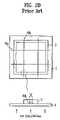
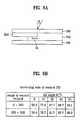
- FIGS. 2A to 2Dillustrate a difference of a hardening rate of a sealant according to a pattern of a light-shielding layer and the sealant formed on a substrate.
- the sealant 7is formed outside a region where the light-shielding layer 8 is formed.
- UV lightis incident upon the sealant 7 even if the UV light is irradiated on the upper substrate 3 where the light-shielding layer 8 is formed.
- the UV lightshould also be irradiated upon the lower substrate 1 to sufficiently cure the sealant 7 from below.
- FIG. 2Dif a metal line layer such as a gate line 6 a and/or a data line 6 b on the lower substrate 1 overlaps the sealant 7 , the UV light is not incident upon the sealant 7 in region A. For this reason, the sealant 7 is not hardened, and adherence between the lower substrate 1 and the upper substrate 3 is reduced.
- the present inventionis directed to a UV irradiating device and a method of manufacturing an LCD device using the same that substantially obviates one or more of the problems due to limitations and disadvantages of the related art.
- An advantage of the present inventionis to provide a UV irradiating device for hardening a sealant and a method of manufacturing an LCD device using the same even if a light-shielding layer or a metal line layer are formed between a UV irradiating surface and a UV sealant.
- a UV irradiating deviceincludes a UV light source part having a UV lamp and a reflecting plate, a support supporting the UV light source part, and a substrate stage on which a substrate is placed, the UV light source being irradiated at a tilt angle upon the substrate.
- the supportis formed at a tilt angle with respect to a horizontal plane
- the substrate stageis formed at a tilt angle with respect to a horizontal plane
- the reflecting plateis formed to allow the light source to be reflected at a tilt angle.
- a method of manufacturing an LCDincludes: preparing lower and upper substrates; forming a UV sealant on one of the lower and upper substrates; applying a liquid crystal on one of the lower and upper substrates; attaching the lower and upper substrates to each other; and irradiating UV upon the attached substrate at a tilt angle.
- the UV lightis irradiated at a tilt angle upon the substrate where the UV sealant is formed, so that the sealant can be hardened even if a light-shielding layer or a metal line layer is formed between a UV irradiating surface and the sealant.
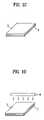
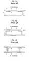
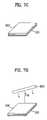
- FIGS. 1A to 1Dare perspective views illustrating a method of manufacturing an LCD device according to a related art liquid crystal application method
- FIGS. 2A to 2Dillustrate a difference of a hardening rate of a sealant according to a pattern of a light-shielding layer and the sealant formed on a substrate;
- FIG. 3is a schematic view of a UV irradiating device according to the first embodiment of the present invention.
- FIGS. 4A and 4Bare schematic views of another UV irradiating device according to the first embodiment of the present invention.
- FIG. 5is a schematic view of a UV irradiating device according to the second embodiment of the present invention.
- FIG. 6is a schematic view of a UV irradiating device according to the third embodiment of the present invention.
- FIGS. 7A to 7Dare perspective views illustrating a method of manufacturing an LCD device in accordance with the principles of the present invention.
- FIG. 8Ais a sectional view illustrating a process of irradiating UV light at a tilt angle ⁇ upon an attached substrate having a light-shielding layer overlapped on a sealant;
- FIG. 8Bis a table illustrating a hardening rate of the sealant according to a change of a tilt angle of ⁇ .
- FIGS. 9A to 9Dare perspective views illustrating a method of manufacturing an LCD device according to the fifth embodiment of the present invention.
- FIGS. 10A to 10Dare perspective views illustrating a process of irradiating UV in the method of manufacturing an LCD device according to the sixth embodiment of the present invention.
- FIG. 11is a layout illustrating a method of manufacturing an LCD according to the present invention.
- FIG. 3is a schematic view of a UV irradiating device according to the first embodiment of the present invention.
- the UV irradiating deviceincludes a UV light source 10 , a support 20 , and a substrate stage 30 on which a substrate to be irradiated with a UV light will be placed.
- the UV light source 10includes a UV lamp 12 and a reflecting plate 14 on which the UV lamp 12 is disposed.
- the support 20supports the UV light source 10 and is moveable to tilt with respect to a horizontal plane.
- a high pressure mercury UV lamp, metal halide UV lamp, or metal UV lampmay be used as the UV lamp 12 .
- the reflecting plate 14shields the UV lamp 12 , and an inner reflecting surface on which the UV lamp 12 is placed such that the irradiated UV is reflected in a constant straight line as shown. Therefore, an irradiating angle of the UV light source depends on the tilt angle of the UV light source 10 .
- the support 20is driven to tilt with respect to a horizontal plane around a driving axis.
- the tilt angle ⁇ 1 of the support 20is within the range of 0° to 90°.
- the UV light source from the UV light source 10is irradiated at an angle of ⁇ with respect to a vertical plane.
- the support 20may be driven upwardly at an angle of ⁇ 1 .
- the driving axis of the support 20may be changed from right of the support 20 to left of the support 20 or may be formed at the center of the support 20 , or at any other location along the support 20 .
- the substrate stage 30is horizontal to receive an attached substrate to which a sealant has been applied. Also, for mass production, the substrate stage 30 may be formed to move by means of a conveyer belt.
- UV irradiating deviceprovided with a plurality of UV light sources may be required.
- FIGS. 4A and 4Bare schematic views of a UV irradiating device provided with a plurality of UV light sources.
- a plurality of UV light sources 10 a , 10 b , and 10 cmay be supported by one support 20 .
- the UV light sources 10 a , 10 b , and 10 cmay respectively be supported by respective supports 20 a , 20 b , and 20 c.
- each respective light source 10 a , 10 b , and 10 c of the UV irradiating device and the substratemay differ.
- the intensity of irradiation from the respective UV light sources onto the substrate surface, and thus onto the sealant to be curedmay differ.
- the distance between each respective UV light source 10 a , 10 b , and 10 c and the substratemay be the same, and, thus, the irradiating characteristics of the UV light from the respective UV light sources 10 a , 10 b , and 10 c may be the same.
- FIG. 5is a schematic view of a UV irradiating device according to the second embodiment of the present invention.
- the UV irradiating deviceincludes a UV light source 10 , a support 20 , and a substrate stage 30 .
- the UV light source 10includes a UV lamp 12 and a reflecting plate 14 on which the UV lamp 12 is disposed.
- the support 20supports the UV light source 10 and is horizontal in a fixed state. A substrate to be irradiated with UV light will be placed on the substrate stage 30 .
- the substrate stage 30is moveable to tilt with respect to a horizontal plane.
- the substrate stage 30is moveable at a tilt angle instead of the support 20 so that a UV light is irradiated upon the substrate stage 30 at a tilt angle.
- a high pressure mercury UV lamp, metal halide UV lamp, or metal UV lampmay be used as the UV lamp 12 .
- the reflecting plate 14shields the UV lamp 12 , and an inner reflecting surface on which the UV lamp 12 is placed is formed such that the irradiated UV is reflected in a constant straight line or collimated.
- the support 20is horizontally placed in a fixed state. Accordingly, the UV light source is vertically irradiated from the UV light source part 10 .
- the substrate stage 30is driven to tilt with respect to a horizontal plane around a driving axis.
- the tilt angle ⁇ of the substrate stage 30is within the range of 0° to 90°.
- the UV light source from the UV light source part 10is irradiated at a tilt angle of ⁇ with respect to a vertical plane of the substrate stage 30 .
- the substrate stage 30may be driven downwardly at an angle of ⁇ .
- the driving axis of the substrate stage 30may be changed from right of the substrate stage 30 to left of the substrate stage 30 or may be formed at the center of the substrate stage 30 or at any other location along the substrate stage 30 .
- a plurality of UV light sourcescan be used for a large substrate so that a large area of the substrate may be irradiated simultaneously.
- FIG. 6is a schematic view of a UV irradiating device according to the third embodiment of the present invention.
- the UV irradiating deviceincludes a UV light source 10 , a support 20 , and a substrate stage 30 .
- the UV light source 10includes a UV lamp 12 and a reflecting plate 14 on which the UV lamp 12 is disposed. Also, the reflecting plate 14 is formed such that a UV light source is irradiated at a tilt angle ⁇ with respect to a vertical plane.
- the support 20supports the UV light source 10 . A substrate to be irradiated with a UV light source will be placed on the substrate stage 30 .
- the support 20 and the substrate stage 30are fixed in horizontal plane (or two parallel planes), and an inner reflecting surface of the reflecting plate 14 is formed so that UV reflected on the reflecting plate 14 is irradiated onto the substrate at a tilt angle.
- a high pressure mercury UV lamp, metal halide UV lamp, or metal UV lampmay be used as the UV lamp 12 .
- the substrate stage 30may be moveable in the horizontal plane or moveable to be tilted with respect to the horizontal plane.
- the UV light from the UV light source 10is irradiated at a tilt angle of ⁇ against a vertical plane of the substrate stage 30 (e.g., at an angle of 90° ⁇ with respect to a horizontal plane if the substrate stage 30 is in the horizontal plane).
- the tilt angle of ⁇can be adjusted by varying a shape of the inner reflecting surface of the reflecting plate 14 .
- FIGS. 7A to 7Dare perspective views illustrating an embodiment of a method of manufacturing an LCD device in accordance with the principles of the present invention.
- a lower substrate 100 and an upper substrate 300are prepared.
- a plurality of gate and data lines(not shown) are formed on the lower substrate 100 .
- the gate linescross the data lines to define a pixel region.
- a thin film transistor(not shown) having a gate electrode, a gate insulating layer, a semiconductor layer, an ohmic contact layer, source/drain electrodes, and a protection layer is formed at a crossing point of the gate lines and the data lines.
- a pixel electrode (not shown) connected with the thin film transistoris formed in the pixel region.
- the alignment filmis formed on the pixel electrode for initial alignment of the liquid crystal.
- the alignment filmmay be formed of polyamide or polyimide based compound, polyvinylalcohol (PVA), and polyamic acid by rubbing.
- the alignment filmmay be formed of a photosensitive material, such as polyvinvylcinnamate (PVCN), polysilioxanecinnamate (PSCN) or cellulosecinnamate (CelCN) based compound, by using photo-alignment method.
- a light-shielding layer(not shown) is formed on the upper substrate 300 to shield light leakage from the gate lines, the data lines, and the thin film transistor regions.
- a color filter layer(not shown) of R, G, and B is formed on the light-shielding layer.
- a common electrode(not shown) is formed on the color filter layer. Additionally, an overcoat layer (not shown) may be formed between the color filter layer and the common electrode. The alignment film is formed on the common electrode.
- Silver (Ag) dotsare formed outside the lower substrate 100 to apply a voltage to the common electrode on the upper substrate 300 after the lower and upper substrates 100 and 300 are bonded to each other.
- the silver dotsmay be formed on the upper substrate 300 .
- the common electrodeis formed on the lower substrate like the pixel electrode so that an electric field can be horizontally induced between the common electrode and the pixel electrode.
- the silver dotsare not formed on the substrates.
- a UV sealant 700is formed on one of the lower and upper substrates 100 and 300 , and a liquid crystal 500 is applied on one of the lower and upper substrates 100 and 300 .
- the liquid crystal 500is applied on the lower substrate 100 to form a liquid crystal layer, and the UV sealant 700 is formed on the upper substrate 300 .
- the liquid crystal 500may be formed on the upper substrate 300 , or the UV sealant 700 may be formed on the lower substrate 100 .
- both the liquid crystal 500 and the UV sealant 700may be formed on one substrate.
- the substratemay not be cleaned even if the sealant is contaminated before the substrates are bonded to each other.
- a cleaning process for cleaning the upper substrate 300may additionally be provided before the bonding process after the UV sealant 700 is formed on the upper strate 300 .
- UV sealant 700monomers or oligomers each having both ends coupled to the acrylic group, mixed with an initiator are used as the UV sealant 700 .
- monomer or oligomers each having one end coupled to the acrylic group and the other end coupled to the epoxy group, mixed with an initiatorare used as the UV sealant 700 .
- Such a UV sealant 700is formed in a closed pattern by using a dispensing method or a screen printing method.
- the liquid crystal 500may be contaminated if it comes into contact with the sealant 700 before the sealant 700 is hardened. Accordingly, the liquid crystal 500 may preferably be applied on the central part of the lower substrate 100 . In this case, the liquid crystal 500 is gradually spread even after the sealant 700 is hardened. Thus, the liquid crystal 500 is uniformly distributed on the surface of the substrate.
- spacersmay be formed on either of the two substrates 100 and 300 to maintain a cell gap.
- the spacersmay be formed on the upper substrate 300 .
- Ball spacers or column spacersmay be used as the spacers.
- the ball spacersmay be formed in such a manner that they are mixed with a solution having an appropriate concentration and then spread at a high pressure onto the substrate from a spray nozzle.
- the column spacersmay be formed on portions of the substrate corresponding to the gate lines or data lines.
- the column spacersmay be used for the large sized substrate since the ball spacers may cause an uneven cell gap for the large sized substrate.
- the column spacersmay be formed of a photosensitive organic resin.
- the lower substrate 100 and the upper substrate 300are attached to each other by the following processes.
- one of the substrates having the liquid crystal applied thereonis placed at the lower side.
- the other substrateis turned by 180 degrees, e.g. flipped so that layers on the upper substrate face the substrate layers on the lower side, and so that the upper substrate is above the lower substrate.
- the substrate at the upper sideis pressed, so that both substrates are attached to each other.
- the space between the substratesmay be maintained under the vacuum state so that both substrates are attached to each other by releasing the vacuum state.
- the attached substrateis horizontally arranged and a UV light source 900 is irradiated at a tilt angle of ⁇ with respect to a plane vertical to the substrate.
- Various light irradiating devices as described in the first and third embodimentsmay be used to irradiate the UV light source 900 at a tilt angle.
- the UV light source 900has been formed above the attached substrate in the drawing, it may be formed below the attached substrate.
- the upper substrate surface or the lower substrate surface of the attached substratemay be used as a UV irradiating surface of the UV light source.
- UV sealantUpon irradiating the UV, monomers or oligomers activated by an initiator constituting the UV sealant are polymerized and hardened, thereby bonding the lower substrate 100 to the upper substrate 300 . If the UV is irradiated at a tilt angle with respect to the substrate, the sealant is hardened even if a light-shielding layer or a metal line layer overlaps the UV sealant. Thus, adherence between the substrates is not comprised.
- the sealant 700may have to be additionally heated at about 120° C. for one hour after the UV irradiation, thereby hardening the sealant completely.
- FIG. 8Ais a sectional view illustrating a process of irradiating UV upon an attached substrate having a light-shielding layer 800 overlapping a sealant 700 at a tilt angle of ⁇ with respect to a plane vertical to the substrate
- FIG. 8Bis a table illustrating a hardening rate of the sealant 700 according to a change of a tilt angle of ⁇ .
- the hardening rate of the sealant 700is 80% or greater.
- the UV lightmay be applied over a range of angle from 0°-90° or 0°-180° or any suitable range, either discretely or continuously.
- the process of cutting a substrate into a unit cell after the UV irradiation and the final test processare performed.
- a cutting lineis formed on a surface of the substrates with a pen or wheel of a material having hardness higher than that of glass, e.g., diamond (scribing process), and then the substrate is cut along the cutting line by mechanical impact (breaking process).
- a pen or wheel of a material having hardness higher than that of glasse.g., diamond
- breaking processe.g., mechanical impact
- the scribing process and the breaking processmay simultaneously be performed using a pen or wheel of a the high hardness material having a toothed shape.
- the final test processis to check whether there are any defects before a unit cell is assembled into a liquid crystal module.
- the liquid crystal moduleis tested to determine whether each pixel is driven properly when a voltage is applied or no voltage is applied.
- FIGS. 9A to 9Dare perspective views illustrating a method of manufacturing an LCD device according to principles of the present invention.
- a lower substrate 100 and an upper substrate 300are prepared.
- a UV sealant 700is formed on the upper substrate 300 , and a liquid crystal is applied on the lower substrate 100 .
- the lower substrate 100 and the upper substrate 300are attached to each other.
- the attached substratesare located tilt and a UV light source 900 is vertically irradiated upon the attached substrates.
- the present embodimentis similar to the previous embodiment of the method except for the UV irradiation process. That is, according to the present embodiment unlike the previous embodiment, the attached substrates are placed at a tilt angle and the UV is vertically irradiated.
- a light irradiating deviceAccording to the second embodiment, a light irradiating device according to the second embodiment can be used.
- FIGS. 10A to 10Dare perspective views illustrating another embodiment of the method of irradiating UV in manufacturing an LCD device according to the present invention.
- the UVmay deteriorate characteristics of devices such as a thin film transistor on the substrate or may change a pre-tilt angle of an alignment film formed for the initial alignment of the liquid crystal.
- UV lightis irradiated at a tilt angle and areas where the sealant is not formed are covered with a mask.
- the attached substratesare placed in a horizontal direction, and a mask 800 that covers the area where the sealant 700 is not formed is placed in parallel with the attached substrates.
- the UV light source 900is then irradiated at a tilt angle.
- the distance between the surface of the attached substrates and the mask 800is within the range of 1 mm to 5 mm.
- the attached substratesare tilted, and the mask 800 that covers the area where the sealant 700 is not formed is placed in parallel with the attached substrates.
- the UV light source 900is vertically irradiated.
- masks 800 and 820 that cover the area that lacks the sealant 700are formed at upper and lower sides of the attached substrates.
- the attached substrates and the masks 800 and 820are placed in a horizontal direction while the UV light source 900 is irradiated at a tilt angle.
- the attached substrates and the masks 800 and 820may be tilted while the UV light source 900 may vertically be irradiated.
- the irradiated UV lightis reflected so that the UV light is prevented from being irradiated upon the area lacking the sealant.
- alignment marks 200 and 850are formed in the attached substrates and the mask 800 to accurately cover the area lacking the sealant 700 .
- the position of the attached substrates and the mask 800is adjusted by a camera 950 checking the alignment marks 200 and 850 .
- the alignment mark 200 of the attached substratesmay be formed on either the upper substrate 300 or the lower substrate 100 of the attached substrates.
- the attached substrates and the mask 800are placed horizontally while the UV light source 900 is irradiated at a tilt angle, the attached substrates and the mask 800 may be tilted while the UV light source 900 may vertically be irradiated.
- the masks with alignment marksmay respectively be formed at upper and lower sides of the attached substrates.
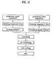
- FIG. 11is a flowchart illustrating a method of manufacturing an LCD according to the present invention.
- an upper substrateis prepared and an alignment film is formed thereon.
- a sealantis then formed on the alignment film, thereby completing the upper substrate.
- a lower substrateis prepared and an alignment film is formed thereon.
- a liquid crystalis then applied on the alignment film, thereby completing the lower substrate.
- the process of manufacturing the upper substrate and the process of manufacturing the lower substrateare simultaneously performed.
- the liquid crystal and the sealantmay selectively be formed on the substrate.
- the completed upper and lower substratesare attached to each other.
- the UV lightis then irradiated to harden the sealant, thereby bonding the substrates.
- the substratesare cut into unit cells, and the final test process is performed, thereby completing one liquid crystal cell.
- the method of manufacturing an LCD according to the present inventionhas the following advantages.
- the UV lightis irradiated at a tilt angle upon the substrates where the UV sealant is formed.
- the sealantcan thus be hardened even if the light shielding layer or the metal line layer is formed between the UV-irradiating surface and the sealant.
- the UV lightis irradiated upon the substrate at a tilt angle in a state that the region where the sealant is not formed is covered with the mask, it is possible to prevent the thin film transistor or the alignment film formed on the substrate from being damaged.
- the substrate stage on which the attached substrates are placedis movably formed, yield is improved.
Landscapes
- Physics & Mathematics (AREA)
- Nonlinear Science (AREA)
- Chemical & Material Sciences (AREA)
- Crystallography & Structural Chemistry (AREA)
- General Physics & Mathematics (AREA)
- Optics & Photonics (AREA)
- Mathematical Physics (AREA)
- Liquid Crystal (AREA)
- Exposure And Positioning Against Photoresist Photosensitive Materials (AREA)
Abstract
Description
Claims (18)
Applications Claiming Priority (2)
| Application Number | Priority Date | Filing Date | Title |
|---|---|---|---|
| KR2002-7130 | 2002-02-07 | ||
| KR1020020007130AKR100672640B1 (en) | 2002-02-07 | 2002-02-07 | UVRadiation device and manufacturing method of liquid crystal display device using same |
Publications (2)
| Publication Number | Publication Date |
|---|---|
| US20030147032A1 US20030147032A1 (en) | 2003-08-07 |
| US7349050B2true US7349050B2 (en) | 2008-03-25 |
Family
ID=27656411
Family Applications (1)
| Application Number | Title | Priority Date | Filing Date |
|---|---|---|---|
| US10/184,077Expired - LifetimeUS7349050B2 (en) | 2002-02-07 | 2002-06-28 | Ultraviolet irradiating device and method of manufacturing liquid crystal display device using the same |
Country Status (4)
| Country | Link |
|---|---|
| US (1) | US7349050B2 (en) |
| JP (1) | JP2003241389A (en) |
| KR (1) | KR100672640B1 (en) |
| CN (1) | CN1325969C (en) |
Cited By (2)
| Publication number | Priority date | Publication date | Assignee | Title |
|---|---|---|---|---|
| US20140170924A1 (en)* | 2012-12-13 | 2014-06-19 | Chengdu Boe Optoelectronics Technology Co., Ltd. | Method for manufacturing a liquid crystal panel |
| US20170191754A1 (en)* | 2016-01-04 | 2017-07-06 | Boe Technology Group Co., Ltd. | Ultraviolet curing device, sealant curing system and sealant curing method |
Families Citing this family (21)
| Publication number | Priority date | Publication date | Assignee | Title |
|---|---|---|---|---|
| TWI304496B (en)* | 2003-03-20 | 2008-12-21 | Sharp Kk | Liquid crystal display apparatus and manufacturing method therefor |
| JP4491773B2 (en)* | 2003-09-26 | 2010-06-30 | 三菱マテリアル株式会社 | Manufacturing method of liquid crystal panel |
| WO2005033788A1 (en)* | 2003-10-08 | 2005-04-14 | Sharp Kabushiki Kaisha | Production method for liquid crystal display panel and ultraviolet irradiation device |
| US8146641B2 (en) | 2003-12-01 | 2012-04-03 | Lg Display Co., Ltd. | Sealant hardening apparatus of liquid crystal display panel and sealant hardening method thereof |
| TWI287657B (en)* | 2004-07-09 | 2007-10-01 | Innolux Display Corp | Curing sealant device, curing sealant method and fabricating method for liquid crystal panel |
| CN100363824C (en)* | 2004-07-13 | 2008-01-23 | 鸿富锦精密工业(深圳)有限公司 | Apparatus and method of frame glue solidification and liquid crystal panel manufacturing method |
| CN100414397C (en)* | 2004-07-16 | 2008-08-27 | 鸿富锦精密工业(深圳)有限公司 | Frame glue solidification method and liquid crystal panel manufacturing method |
| WO2008072528A1 (en)* | 2006-12-08 | 2008-06-19 | Canon Kabushiki Kaisha | Liquid crystal optical device manufacturing process |
| KR101065641B1 (en)* | 2009-07-09 | 2011-09-19 | 주식회사 엘티에스 | Sealing system and sealing method of flat panel display |
| US20130288411A1 (en)* | 2012-04-26 | 2013-10-31 | Shaoxin Yu | Manufacturing device and method of liquid crystal panel |
| KR102178750B1 (en)* | 2014-06-20 | 2020-11-16 | 엘지디스플레이 주식회사 | Apparatus And Method For Hardening Resin |
| CN104375327B (en)* | 2014-11-20 | 2017-10-27 | 上海天马微电子有限公司 | Liquid crystal display device and manufacturing method thereof |
| KR102224443B1 (en) | 2014-12-10 | 2021-03-09 | 엘지디스플레이 주식회사 | Liquid Crystal Display Device |
| JP2016147231A (en)* | 2015-02-12 | 2016-08-18 | 東レエンジニアリング株式会社 | Coating apparatus |
| CN204406005U (en)* | 2015-02-28 | 2015-06-17 | 成都京东方光电科技有限公司 | Light orientation apparatus |
| CN104815533B (en)* | 2015-04-21 | 2017-05-10 | 中山火炬职业技术学院 | A non-body VOC emission reduction device in offset printing workshop using UV curing |
| JP2018521884A (en) | 2015-07-20 | 2018-08-09 | スリーエム イノベイティブ プロパティズ カンパニー | Actinic radiation equipment for rapid curing of resins |
| KR20170058182A (en)* | 2015-11-18 | 2017-05-26 | (주)쎄미시스코 | Light Sintering Apparatus Having Inclined Feeding Part for Fume Removal |
| CN107463063A (en)* | 2017-08-02 | 2017-12-12 | 深圳市华星光电技术有限公司 | Ultraviolet light solidification mask plate and preparation method thereof and curing |
| CN111752048B (en)* | 2019-03-29 | 2023-07-04 | 夏普株式会社 | Liquid crystal display device having a light shielding layer |
| CN109856866B (en)* | 2019-04-04 | 2020-10-13 | 深圳市华星光电技术有限公司 | Frame sealing glue curing device and curing method thereof |
Citations (253)
| Publication number | Priority date | Publication date | Assignee | Title |
|---|---|---|---|---|
| JPS5165656A (en) | 1974-12-04 | 1976-06-07 | Shinshu Seiki Kk | |
| US3978580A (en) | 1973-06-28 | 1976-09-07 | Hughes Aircraft Company | Method of fabricating a liquid crystal display |
| US4094058A (en) | 1976-07-23 | 1978-06-13 | Omron Tateisi Electronics Co. | Method of manufacture of liquid crystal displays |
| JPS5738414A (en) | 1980-08-20 | 1982-03-03 | Showa Denko Kk | Spacer for display panel |
| JPS5788428A (en) | 1980-11-20 | 1982-06-02 | Ricoh Elemex Corp | Manufacture of liquid crystal display body device |
| JPS5827126A (en) | 1981-08-11 | 1983-02-17 | Nec Corp | Production of liquid crystal display panel |
| JPS5957221A (en) | 1982-09-28 | 1984-04-02 | Asahi Glass Co Ltd | Production of display element |
| JPS59195222A (en) | 1983-04-19 | 1984-11-06 | Matsushita Electric Ind Co Ltd | Manufacture of liquid-crystal panel |
| JPS60111221A (en) | 1983-11-19 | 1985-06-17 | Nippon Denso Co Ltd | Method and device for charging liquid crystal |
| JPS60164723A (en) | 1984-02-07 | 1985-08-27 | Seiko Instr & Electronics Ltd | Liquid crystal display device |
| JPS60217343A (en) | 1984-04-13 | 1985-10-30 | Matsushita Electric Ind Co Ltd | Liquid crystal display device and its preparation |
| JPS617822A (en) | 1984-06-22 | 1986-01-14 | Canon Inc | Production of liquid crystal element |
| JPS6155625A (en) | 1984-08-24 | 1986-03-20 | Nippon Denso Co Ltd | Manufacture of liquid crystal element |
| JPS6254229A (en) | 1985-07-15 | 1987-03-09 | Semiconductor Energy Lab Co Ltd | Manufacturing method for liquid crystal display |
| JPS6254228A (en) | 1985-07-15 | 1987-03-09 | Semiconductor Energy Lab Co Ltd | Manufacturing method for liquid crystal display |
| JPS6254225A (en) | 1985-07-15 | 1987-03-09 | Semiconductor Energy Lab Co Ltd | Manufacturing method for liquid crystal display |
| US4653864A (en) | 1986-02-26 | 1987-03-31 | Ovonic Imaging Systems, Inc. | Liquid crystal matrix display having improved spacers and method of making same |
| JPS6289025A (en) | 1985-10-15 | 1987-04-23 | Matsushita Electric Ind Co Ltd | Manufacturing method of liquid crystal display panel |
| JPS6290622A (en) | 1985-10-17 | 1987-04-25 | Seiko Epson Corp | liquid crystal display device |
| US4691995A (en) | 1985-07-15 | 1987-09-08 | Semiconductor Energy Laboratory Co., Ltd. | Liquid crystal filling device |
| JPS62205319A (en) | 1986-03-06 | 1987-09-09 | Canon Inc | Ferroelectric liquid crystal element |
| JPS63109413A (en) | 1986-10-27 | 1988-05-14 | Fujitsu Ltd | Manufacturing method of LCD display |
| JPS63110425A (en) | 1986-10-29 | 1988-05-14 | Toppan Printing Co Ltd | Cell for liquid crystal filling |
| JPS63128315A (en) | 1986-11-19 | 1988-05-31 | Victor Co Of Japan Ltd | Liquid crystal display element |
| US4775225A (en) | 1985-05-16 | 1988-10-04 | Canon Kabushiki Kaisha | Liquid crystal device having pillar spacers with small base periphery width in direction perpendicular to orientation treatment |
| JPS63311233A (en) | 1987-06-12 | 1988-12-20 | Toyota Motor Corp | lcd cell |
| JPH039549A (en) | 1989-05-16 | 1991-01-17 | Motorola Inc | Composite integrated storage device |
| JPH0536425A (en) | 1991-02-12 | 1993-02-12 | Tokyo Electric Power Co Inc:The | Alloy separator for solid oxide fuel cell and method for producing the same |
| JPH0536426A (en) | 1991-07-31 | 1993-02-12 | Mitsubishi Heavy Ind Ltd | Solid electrolytic fuel cell |
| JPH05107533A (en) | 1991-10-16 | 1993-04-30 | Shinetsu Eng Kk | Method for laminating glass substrate for liquid crystal display panel and laminating apparatus therefor |
| JPH05127179A (en) | 1991-11-01 | 1993-05-25 | Ricoh Co Ltd | Production of liquid crystal display element |
| JPH05154923A (en) | 1991-12-06 | 1993-06-22 | Hitachi Ltd | Substrate assembling device |
| US5247377A (en) | 1988-07-23 | 1993-09-21 | Rohm Gmbh Chemische Fabrik | Process for producing anisotropic liquid crystal layers on a substrate |
| JPH05265011A (en) | 1992-03-19 | 1993-10-15 | Seiko Instr Inc | Production of liquid crystal display element |
| JPH05281562A (en) | 1992-04-01 | 1993-10-29 | Matsushita Electric Ind Co Ltd | Manufacture of liquid crystal panel |
| JPH05281557A (en) | 1992-04-01 | 1993-10-29 | Matsushita Electric Ind Co Ltd | Liquid crystal panel manufacturing method |
| US5263888A (en) | 1992-02-20 | 1993-11-23 | Matsushita Electric Industrial Co., Ltd. | Method of manufacture of liquid crystal display panel |
| JPH0618829A (en) | 1992-06-30 | 1994-01-28 | Shinetsu Eng Kk | Device for laminating glass substrates for liquid crystal display boards |
| JPH0651256A (en) | 1992-07-30 | 1994-02-25 | Matsushita Electric Ind Co Ltd | Device for discharging liquid crystal |
| JPH0664229A (en) | 1992-08-24 | 1994-03-08 | Toshiba Corp | Optical printing head |
| JPH06148657A (en) | 1992-11-06 | 1994-05-27 | Matsushita Electric Ind Co Ltd | Method of manufacturing cell for liquid crystal display and manufacturing apparatus thereof |
| JPH06160871A (en) | 1992-11-26 | 1994-06-07 | Matsushita Electric Ind Co Ltd | Liquid crystal display panel and manufacturing method thereof |
| JPH06194637A (en) | 1992-12-24 | 1994-07-15 | Shinetsu Eng Kk | Method for sticking glass substrate for liquid crystal display plate |
| JPH06235925A (en) | 1993-02-10 | 1994-08-23 | Matsushita Electric Ind Co Ltd | Manufacture of liquid crystal display element |
| JPH06265915A (en) | 1993-03-12 | 1994-09-22 | Matsushita Electric Ind Co Ltd | Discharge device for filling liquid crystal |
| JPH06313870A (en) | 1993-04-28 | 1994-11-08 | Hitachi Ltd | Substrate assembly device |
| US5379139A (en) | 1986-08-20 | 1995-01-03 | Semiconductor Energy Laboratory Co., Ltd. | Liquid crystal device and method for manufacturing same with spacers formed by photolithography |
| JPH0784268A (en) | 1993-09-13 | 1995-03-31 | Hitachi Ltd | Sealing agent drawing method |
| US5406989A (en) | 1993-10-12 | 1995-04-18 | Ayumi Industry Co., Ltd. | Method and dispenser for filling liquid crystal into LCD cell |
| JPH07128674A (en) | 1993-11-05 | 1995-05-19 | Matsushita Electric Ind Co Ltd | Liquid crystal display element manufacturing method |
| JPH07181507A (en) | 1993-12-21 | 1995-07-21 | Canon Inc | Liquid crystal display device and information transmission device including the liquid crystal display device |
| JPH07275770A (en) | 1994-04-06 | 1995-10-24 | Hitachi Techno Eng Co Ltd | Paste applicator |
| JPH07275771A (en) | 1994-04-11 | 1995-10-24 | Hitachi Techno Eng Co Ltd | Paste applicator |
| JPH07333624A (en) | 1994-06-07 | 1995-12-22 | Hitachi Ltd | Method of manufacturing liquid crystal display device and light-shielding mask for curing encapsulant |
| US5499128A (en) | 1993-03-15 | 1996-03-12 | Kabushiki Kaisha Toshiba | Liquid crystal display device with acrylic polymer spacers and method of manufacturing the same |
| JPH0876133A (en) | 1994-09-02 | 1996-03-22 | Shinetsu Eng Kk | Surface plate structure in a bonding apparatus for glass substrates for liquid crystal display boards |
| JPH0895066A (en) | 1994-09-27 | 1996-04-12 | Matsushita Electric Ind Co Ltd | Method and apparatus for manufacturing liquid crystal element |
| US5507323A (en) | 1993-10-12 | 1996-04-16 | Fujitsu Limited | Method and dispenser for filling liquid crystal into LCD cell |
| JPH08101395A (en) | 1994-09-30 | 1996-04-16 | Matsushita Electric Ind Co Ltd | Liquid crystal display element manufacturing method |
| JPH08106101A (en) | 1994-10-06 | 1996-04-23 | Fujitsu Ltd | Liquid crystal display panel manufacturing method |
| JPH08110504A (en) | 1994-10-13 | 1996-04-30 | Shinetsu Eng Kk | Glass substrate heating device for liquid crystal display panel |
| JPH08136937A (en) | 1994-11-09 | 1996-05-31 | Shinetsu Eng Kk | Method and apparatus for pressurizing and heating glass substrate for liquid crystal display panel |
| JPH08171094A (en) | 1994-12-19 | 1996-07-02 | Nippon Soken Inc | Liquid crystal injecting method and liquid crystal injecting device to liquid crystal display device |
| JPH08173874A (en) | 1994-12-26 | 1996-07-09 | Hitachi Techno Eng Co Ltd | Paste applicator |
| JPH08190099A (en) | 1995-01-11 | 1996-07-23 | Fujitsu Ltd | Liquid crystal display device manufacturing method and liquid crystal display device manufacturing apparatus |
| US5539545A (en) | 1993-05-18 | 1996-07-23 | Semiconductor Energy Laboratory Co., Ltd. | Method of making LCD in which resin columns are cured and the liquid crystal is reoriented |
| US5548429A (en) | 1993-06-14 | 1996-08-20 | Canon Kabushiki Kaisha | Process for producing liquid crystal device whereby curing the sealant takes place after pre-baking the substrates |
| JPH08210911A (en) | 1995-02-02 | 1996-08-20 | Canon Inc | Ultraviolet intensity distribution measuring method, its apparatus, optical component mounting method, and prism fixing method |
| JPH08240807A (en) | 1995-03-06 | 1996-09-17 | Fujitsu Ltd | Liquid crystal display panel sealing method |
| JPH08304836A (en) | 1995-04-28 | 1996-11-22 | Hitachi Electron Eng Co Ltd | Ultraviolet ray sealing material curing device |
| JPH091026A (en) | 1995-06-23 | 1997-01-07 | Hitachi Techno Eng Co Ltd | Paste applicator |
| JPH095762A (en) | 1995-06-20 | 1997-01-10 | Matsushita Electric Ind Co Ltd | Liquid crystal panel manufacturing method |
| JPH0926578A (en) | 1995-07-10 | 1997-01-28 | Fujitsu Ltd | Liquid crystal display panel and method of manufacturing the same |
| US5604615A (en)* | 1994-05-27 | 1997-02-18 | Sharp Kabushiki Kaisha | Liquid crystal display device and methods for producing same with alignment layer having new bond formation or bond cleavage reaction of molecular chains by light irradiation |
| US5608550A (en)* | 1994-06-24 | 1997-03-04 | Minnesota Mining And Manufacturing Company | Front-lit liquid crystal display having brightness enhancing film with microridges which directs light through the display to a reflector |
| JPH0961829A (en) | 1995-08-21 | 1997-03-07 | Matsushita Electric Ind Co Ltd | Liquid crystal display element manufacturing method |
| JPH0973096A (en) | 1995-09-05 | 1997-03-18 | Matsushita Electric Ind Co Ltd | Liquid crystal display element manufacturing method |
| JPH0973075A (en) | 1995-09-05 | 1997-03-18 | Matsushita Electric Ind Co Ltd | Liquid crystal display element manufacturing method and liquid crystal display element manufacturing apparatus |
| JPH0994500A (en) | 1995-09-29 | 1997-04-08 | Hitachi Techno Eng Co Ltd | Paste applicator |
| JPH09127528A (en) | 1995-10-27 | 1997-05-16 | Fujitsu Ltd | Liquid crystal panel manufacturing method |
| US5636043A (en)* | 1993-08-25 | 1997-06-03 | Matsushita Electric Industrial Co., Ltd. | Liquid crystal display device having partitioned unit liquid crystal cells |
| US5642214A (en) | 1991-07-19 | 1997-06-24 | Sharp Kabushiki Kaisha | Optical modulating element and electronic apparatus using it |
| JPH09230357A (en) | 1996-02-22 | 1997-09-05 | Canon Inc | Liquid crystal panel manufacturing method and liquid crystal cell used therefor |
| US5680185A (en)* | 1990-11-26 | 1997-10-21 | Seiko Epson Corporation | Polymer dispersed liquid crystal (PDLC) display apparatus |
| JPH09281511A (en) | 1996-04-17 | 1997-10-31 | Fujitsu Ltd | Liquid crystal display panel manufacturing method |
| JPH09311340A (en) | 1996-05-21 | 1997-12-02 | Matsushita Electric Ind Co Ltd | Liquid crystal display manufacturing method |
| US5742370A (en) | 1996-09-12 | 1998-04-21 | Korea Institute Of Science And Technology | Fabrication method for liquid crystal alignment layer by magnetic field treatment |
| JPH10104590A (en) | 1996-09-26 | 1998-04-24 | Toshiba Corp | Liquid crystal cell assembly equipment |
| JPH10123538A (en) | 1996-10-22 | 1998-05-15 | Matsushita Electric Ind Co Ltd | Manufacturing method of liquid crystal display element |
| JPH10123537A (en) | 1996-10-15 | 1998-05-15 | Matsushita Electric Ind Co Ltd | Liquid crystal display device and method of manufacturing the same |
| US5757451A (en) | 1995-09-08 | 1998-05-26 | Kabushiki Kaisha Toshiba | Liquid crystal display device spacers formed from stacked color layers |
| JPH10142616A (en) | 1996-11-14 | 1998-05-29 | Ayumi Kogyo Kk | Liquid crystal injection method and liquid dispenser |
| JPH10154658A (en) | 1996-09-27 | 1998-06-09 | Ushio Inc | Proximity exposure system with variable irradiation angle |
| US5767935A (en)* | 1995-08-31 | 1998-06-16 | Sumitomo Chemical Company, Limited | Light control sheet and liquid crystal display device comprising the same |
| JPH10174924A (en) | 1996-12-17 | 1998-06-30 | Hitachi Techno Eng Co Ltd | Paste coating machine |
| JPH10177178A (en) | 1996-12-17 | 1998-06-30 | Matsushita Electric Ind Co Ltd | Manufacturing method of liquid crystal display element |
| US5783338A (en)* | 1996-02-09 | 1998-07-21 | Lc Electronics Inc. | Method for manufacturing black matrix of active matrix liquid crystal display |
| JPH10221700A (en) | 1997-02-10 | 1998-08-21 | Fujitsu Ltd | Manufacturing method of liquid crystal display device |
| US5798809A (en)* | 1996-08-16 | 1998-08-25 | Fujitsu Limited | Liquid crystal display panel |
| JPH10282512A (en) | 1997-04-07 | 1998-10-23 | Ayumi Kogyo Kk | Liquid crystal injection method and dispenser used therefor |
| JPH10333159A (en) | 1997-06-03 | 1998-12-18 | Matsushita Electric Ind Co Ltd | Liquid crystal display |
| JPH10333157A (en) | 1997-06-03 | 1998-12-18 | Matsushita Electric Ind Co Ltd | Manufacturing method of liquid crystal display device |
| US5852484A (en) | 1994-09-26 | 1998-12-22 | Matsushita Electric Industrial Co., Ltd. | Liquid crystal display panel and method and device for manufacturing the same |
| US5861932A (en) | 1997-03-31 | 1999-01-19 | Denso Corporation | Liquid crystal cell and its manufacturing method |
| JPH1114953A (en) | 1997-06-20 | 1999-01-22 | Matsushita Electric Ind Co Ltd | Method of manufacturing multi-touch liquid crystal display panel and multi-touch liquid crystal display panel |
| JPH1138424A (en) | 1997-07-23 | 1999-02-12 | Fujitsu Ltd | Liquid crystal display panel and method of manufacturing the same |
| US5875922A (en) | 1997-10-10 | 1999-03-02 | Nordson Corporation | Apparatus for dispensing an adhesive |
| JPH1164811A (en) | 1997-08-21 | 1999-03-05 | Matsushita Electric Ind Co Ltd | Method and apparatus for manufacturing liquid crystal display element |
| US5889571A (en)* | 1996-02-01 | 1999-03-30 | Lg Electronics Inc. | Ultraviolet irradiating device for photo-alignment process and an irradiating method using the same |
| JPH11109388A (en) | 1997-10-03 | 1999-04-23 | Hitachi Ltd | Manufacturing method of liquid crystal display device |
| JPH11133438A (en) | 1997-10-24 | 1999-05-21 | Matsushita Electric Ind Co Ltd | Liquid crystal display device and its manufacturing method |
| JPH11142864A (en) | 1997-11-07 | 1999-05-28 | Matsushita Electric Ind Co Ltd | Manufacturing method of liquid crystal display device |
| JPH11174477A (en) | 1997-12-08 | 1999-07-02 | Matsushita Electric Ind Co Ltd | Manufacturing method of liquid crystal display device |
| JPH11212045A (en) | 1998-01-26 | 1999-08-06 | Matsushita Electric Ind Co Ltd | Liquid crystal panel manufacturing method |
| US5936688A (en)* | 1996-02-27 | 1999-08-10 | Sharp Kabushiki Kaisha | Reflector, method for fabricating the same and reflective liquid crystal display device incorporating the same |
| US5934780A (en)* | 1996-09-12 | 1999-08-10 | Ushiodenki Kabushiki Kaisha | Polarized light irradiation device for purposes of optical alignment of an alignment layer of a liquid crystal cell element |
| US5952678A (en) | 1995-01-23 | 1999-09-14 | Mitsubishi Denki Kabushiki Kaisha | SRAM cell with no PN junction between driver and load transistors and method of manufacturing the same |
| JPH11248930A (en) | 1998-03-06 | 1999-09-17 | Matsushita Electric Ind Co Ltd | Color filter substrate, method of manufacturing the color filter substrate, and liquid crystal display device using the color filter substrate |
| US5956112A (en) | 1995-10-02 | 1999-09-21 | Sharp Kabushiki Kaisha | Liquid crystal display device and method for manufacturing the same |
| JPH11264991A (en) | 1998-01-13 | 1999-09-28 | Matsushita Electric Ind Co Ltd | Manufacturing method of liquid crystal display element |
| JPH11262712A (en) | 1998-03-17 | 1999-09-28 | Hitachi Techno Eng Co Ltd | Paste application method and paste application machine |
| JPH11326922A (en) | 1998-05-14 | 1999-11-26 | Matsushita Electric Ind Co Ltd | Liquid crystal display panel manufacturing method |
| JPH11344714A (en) | 1998-06-02 | 1999-12-14 | Denso Corp | Liquid crystal cell |
| US6001203A (en) | 1995-03-01 | 1999-12-14 | Matsushita Electric Industrial Co., Ltd. | Production process of liquid crystal display panel, seal material for liquid crystal cell and liquid crystal display |
| US6011609A (en) | 1996-10-05 | 2000-01-04 | Samsung Electronics Co., Ltd. | Method of manufacturing LCD by dropping liquid crystals on a substrate and then pressing the substrates |
| JP2000002879A (en) | 1998-06-12 | 2000-01-07 | Matsushita Electric Ind Co Ltd | Apparatus and method for assembling liquid crystal panel |
| US6016178A (en) | 1996-09-13 | 2000-01-18 | Sony Corporation | Reflective guest-host liquid-crystal display device |
| US6016181A (en) | 1996-11-07 | 2000-01-18 | Sharp Kabushiki Kaisha | Liquid crystal device having column spacers with portion on each of the spacers for reflecting or absorbing visible light and method for fabricating the same |
| JP2000029035A (en) | 1998-07-09 | 2000-01-28 | Minolta Co Ltd | Liquid crystal element and its manufacture |
| JP2000056311A (en) | 1998-08-03 | 2000-02-25 | Matsushita Electric Ind Co Ltd | Liquid crystal display |
| JP2000066165A (en) | 1998-08-20 | 2000-03-03 | Matsushita Electric Ind Co Ltd | Liquid crystal display panel manufacturing method |
| JP2000066218A (en) | 1998-08-21 | 2000-03-03 | Shinetsu Engineering Kk | LCD panel manufacturing equipment |
| JP2000093866A (en) | 1998-09-18 | 2000-04-04 | Hitachi Techno Eng Co Ltd | Paste application method and paste application machine |
| US6055035A (en) | 1998-05-11 | 2000-04-25 | International Business Machines Corporation | Method and apparatus for filling liquid crystal display (LCD) panels |
| JP2000137235A (en) | 1998-11-02 | 2000-05-16 | Matsushita Electric Ind Co Ltd | Liquid crystal substrate bonding method |
| EP1003066A1 (en) | 1998-11-16 | 2000-05-24 | Matsushita Electric Industrial Co., Ltd. | Method of manufacturing liquid crystal display devices |
| JP2000193988A (en) | 1998-12-25 | 2000-07-14 | Fujitsu Ltd | Method and apparatus for manufacturing liquid crystal display panel |
| JP2000206701A (en) | 1999-01-12 | 2000-07-28 | Sharp Corp | Exposure equipment |
| JP2000241824A (en) | 1999-02-18 | 2000-09-08 | Matsushita Electric Ind Co Ltd | Manufacturing method of liquid crystal display device |
| JP2000284295A (en) | 1999-03-30 | 2000-10-13 | Hitachi Techno Eng Co Ltd | Substrate assembling method and apparatus |
| JP2000292799A (en) | 1999-04-09 | 2000-10-20 | Matsushita Electric Ind Co Ltd | Liquid crystal display device and method of manufacturing the same |
| JP2000310759A (en) | 1999-04-28 | 2000-11-07 | Matsushita Electric Ind Co Ltd | Liquid crystal display device manufacturing apparatus and method |
| JP2000310784A (en) | 1999-02-22 | 2000-11-07 | Matsushita Electric Ind Co Ltd | Liquid crystal panel, color filter and method for producing them |
| JP2000338501A (en) | 1999-05-26 | 2000-12-08 | Matsushita Electric Ind Co Ltd | Liquid crystal display panel manufacturing method |
| US6163357A (en) | 1996-09-26 | 2000-12-19 | Kabushiki Kaisha Toshiba | Liquid crystal display device having the driving circuit disposed in the seal area, with different spacer density in driving circuit area than display area |
| US6166793A (en)* | 1997-06-06 | 2000-12-26 | Sumitomo Chemical Company, Limited | Reflective liquid crystal display with angularly selective light diffuser directly on reflector |
| JP2001005405A (en) | 1999-06-18 | 2001-01-12 | Hitachi Techno Eng Co Ltd | Substrate assembling method and apparatus |
| JP2001005401A (en) | 1999-06-21 | 2001-01-12 | Hitachi Techno Eng Co Ltd | Substrate assembling method and apparatus |
| US6175397B1 (en)* | 1997-03-10 | 2001-01-16 | Canon Kabushiki Kaisha | Liquid crystal display apparatus, a liquid crystal projector using same, and a method of manufacturing the liquid crystal display apparatus |
| JP2001013506A (en) | 1999-04-30 | 2001-01-19 | Matsushita Electric Ind Co Ltd | Liquid crystal display device and method of manufacturing the same |
| JP2001033793A (en) | 1999-07-21 | 2001-02-09 | Matsushita Electric Ind Co Ltd | Liquid crystal display panel and method of manufacturing the same |
| JP2001042341A (en) | 1999-08-03 | 2001-02-16 | Hitachi Techno Eng Co Ltd | How to assemble a liquid crystal substrate |
| US6191836B1 (en)* | 1996-11-07 | 2001-02-20 | Lg Philips Lcd, Co., Ltd. | Method for fabricating a liquid crystal cell |
| JP2001051284A (en) | 1999-08-10 | 2001-02-23 | Matsushita Electric Ind Co Ltd | Liquid crystal display device manufacturing equipment |
| JP2001066615A (en) | 2000-08-02 | 2001-03-16 | Matsushita Electric Ind Co Ltd | Manufacturing method of liquid crystal display device |
| US6206527B1 (en)* | 1998-11-24 | 2001-03-27 | Ushiodenki Kabushiki Kaisha | Device for oblique light irradiation |
| JP2001091727A (en) | 1999-09-27 | 2001-04-06 | Matsushita Electric Ind Co Ltd | Method for manufacturing color filter substrate, color filter substrate and liquid crystal display device |
| US6219126B1 (en) | 1998-11-20 | 2001-04-17 | International Business Machines Corporation | Panel assembly for liquid crystal displays having a barrier fillet and an adhesive fillet in the periphery |
| JP2001117105A (en) | 1999-10-18 | 2001-04-27 | Toshiba Corp | Manufacturing method of liquid crystal display device |
| JP2001117109A (en) | 1999-10-21 | 2001-04-27 | Matsushita Electric Ind Co Ltd | Manufacturing method of liquid crystal display device |
| US6226067B1 (en) | 1997-10-03 | 2001-05-01 | Minolta Co., Ltd. | Liquid crystal device having spacers and manufacturing method thereof |
| US6226066B1 (en)* | 1996-01-09 | 2001-05-01 | Lg. Philips Lcd Co., Ltd. | Method for controlling pretilt angle direction in a liquid crystal cell |
| KR20010040083A (en) | 1999-10-22 | 2001-05-15 | 포만 제프리 엘 | A method and system for curing ultra violet curable sealant that is shadowed by metallization |
| JP2001133745A (en) | 1999-11-08 | 2001-05-18 | Hitachi Techno Eng Co Ltd | Substrate assembling method and apparatus |
| JP2001133794A (en) | 1999-11-01 | 2001-05-18 | Kyoritsu Kagaku Sangyo Kk | Sealing agent for dropping process of lcd panel |
| US6236445B1 (en) | 1996-02-22 | 2001-05-22 | Hughes Electronics Corporation | Method for making topographic projections |
| JP2001142074A (en) | 1999-11-10 | 2001-05-25 | Hitachi Ltd | Liquid crystal display |
| JP2001147437A (en) | 1999-11-19 | 2001-05-29 | Nec Corp | Liquid crystal display panel and method of producing the same |
| JP2001154211A (en) | 1999-11-30 | 2001-06-08 | Hitachi Ltd | Liquid crystal panel and method of manufacturing the same |
| JP2001166272A (en) | 1999-12-09 | 2001-06-22 | Hitachi Techno Eng Co Ltd | Substrate assembling method and apparatus |
| JP2001166310A (en) | 1999-12-08 | 2001-06-22 | Matsushita Electric Ind Co Ltd | Liquid crystal display panel manufacturing method |
| JP2001183683A (en) | 1999-10-05 | 2001-07-06 | Matsushita Electric Ind Co Ltd | Liquid crystal display panel and method of manufacturing and driving the same |
| JP2001201750A (en) | 2000-01-14 | 2001-07-27 | Fujitsu Ltd | Liquid crystal display device and method of manufacturing the same |
| JP2001209056A (en) | 2000-01-25 | 2001-08-03 | Shinetsu Engineering Kk | LCD panel manufacturing equipment |
| JP2001209057A (en) | 2000-01-26 | 2001-08-03 | Shinetsu Engineering Kk | LCD panel manufacturing equipment |
| JP2001209058A (en) | 2000-01-26 | 2001-08-03 | Shinetsu Engineering Kk | LCD panel manufacturing equipment |
| JP2001209060A (en) | 2000-12-11 | 2001-08-03 | Fujitsu Ltd | Liquid crystal display panel manufacturing method |
| JP2001209052A (en) | 2000-01-24 | 2001-08-03 | Matsushita Electric Ind Co Ltd | Liquid crystal display device and method of manufacturing the same |
| JP2001215459A (en) | 2000-02-02 | 2001-08-10 | Matsushita Electric Ind Co Ltd | Liquid crystal display device manufacturing equipment |
| JP2001222017A (en) | 1999-05-24 | 2001-08-17 | Fujitsu Ltd | Liquid crystal display device and method of manufacturing the same |
| JP2001235758A (en) | 2000-02-23 | 2001-08-31 | Fujitsu Ltd | Liquid crystal display panel and method of manufacturing the same |
| JP2001255542A (en) | 2000-03-14 | 2001-09-21 | Sharp Corp | Substrate bonding method and substrate bonding apparatus, and method and apparatus for manufacturing liquid crystal display element |
| US6295110B1 (en)* | 1997-11-05 | 2001-09-25 | Hitachi, Ltd. | Liquid crystal display device having orientation film oriented by light |
| JP2001264782A (en) | 2000-03-16 | 2001-09-26 | Ayumi Kogyo Kk | Filling method of mucous material between flat panel substrates |
| JP2001272640A (en) | 2000-03-27 | 2001-10-05 | Fujitsu Ltd | Liquid crystal dropping device and liquid crystal dropping method |
| JP2001281678A (en) | 2000-03-29 | 2001-10-10 | Fujitsu Ltd | Manufacturing method of liquid crystal display device |
| JP2001281675A (en) | 2000-03-29 | 2001-10-10 | Matsushita Electric Ind Co Ltd | Manufacturing method of liquid crystal display device |
| JP2001282126A (en) | 2000-03-30 | 2001-10-12 | Hitachi Techno Eng Co Ltd | Board assembly equipment |
| US6304306B1 (en) | 1995-02-17 | 2001-10-16 | Sharp Kabushiki Kaisha | Liquid crystal display device and method for producing the same |
| US6307609B1 (en)* | 1997-08-05 | 2001-10-23 | Wayne M. Gibbons | Polarized light exposure systems for aligning liquid crystals |
| JP2001305563A (en) | 2000-04-19 | 2001-10-31 | Hitachi Techno Eng Co Ltd | Substrate bonding device |
| US6313894B1 (en)* | 1997-03-10 | 2001-11-06 | Canon Kabushiki Kaisha | Liquid crystal display |
| JP2001330840A (en) | 2000-05-18 | 2001-11-30 | Toshiba Corp | Manufacturing method of liquid crystal display element |
| JP2001330837A (en) | 2000-05-19 | 2001-11-30 | Matsushita Electric Ind Co Ltd | Hermetic structure, method of manufacturing the same, liquid crystal display device using the same, and method of manufacturing the same |
| JP2001356353A (en) | 2001-04-24 | 2001-12-26 | Hitachi Industries Co Ltd | Board assembly equipment |
| JP2001356354A (en) | 2000-06-13 | 2001-12-26 | Matsushita Electric Ind Co Ltd | Manufacturing method of liquid crystal display element |
| US6337730B1 (en) | 1998-06-02 | 2002-01-08 | Denso Corporation | Non-uniformly-rigid barrier wall spacers used to correct problems caused by thermal contraction of smectic liquid crystal material |
| US6339459B1 (en)* | 1997-11-06 | 2002-01-15 | Canon Kabushiki Kaisha | Liquid crystal display device |
| JP2002014360A (en) | 2000-06-29 | 2002-01-18 | Matsushita Electric Ind Co Ltd | Method and apparatus for manufacturing liquid crystal panel |
| JP2002023176A (en) | 2000-07-05 | 2002-01-23 | Seiko Epson Corp | Liquid crystal injection device and liquid crystal injection method |
| JP2002049045A (en) | 2000-08-03 | 2002-02-15 | Nec Corp | Method for manufacturing liquid crystal display panel |
| JP2002079160A (en) | 2000-09-04 | 2002-03-19 | Hitachi Industries Co Ltd | Paste coating machine |
| JP2002080321A (en) | 2000-06-20 | 2002-03-19 | Kyowa Hakko Kogyo Co Ltd | Cosmetic |
| JP2002082340A (en) | 2000-09-08 | 2002-03-22 | Fuji Xerox Co Ltd | Method for manufacturing flat panel display |
| JP2002090760A (en) | 2000-09-12 | 2002-03-27 | Matsushita Electric Ind Co Ltd | Liquid crystal display panel manufacturing apparatus and method |
| JP2002090758A (en) | 2000-09-12 | 2002-03-27 | Matsushita Electric Ind Co Ltd | Liquid crystal display panel manufacturing apparatus and method |
| JP2002090759A (en) | 2000-09-18 | 2002-03-27 | Sharp Corp | Apparatus and method for manufacturing liquid crystal display element |
| JP2002107740A (en) | 2000-09-28 | 2002-04-10 | Sharp Corp | Method and apparatus for manufacturing liquid crystal display panel |
| JP2002122872A (en) | 2000-10-12 | 2002-04-26 | Hitachi Ltd | Liquid crystal display device and manufacturing method thereof |
| JP2002122873A (en) | 2000-10-13 | 2002-04-26 | Stanley Electric Co Ltd | Liquid crystal device manufacturing method |
| JP2002122870A (en) | 2000-10-13 | 2002-04-26 | Fujitsu Ltd | Liquid crystal display device, manufacturing method thereof, and liquid crystal dropping device |
| JP2002131762A (en) | 2000-10-30 | 2002-05-09 | Shinetsu Engineering Kk | Apparatus and method for bonding liquid crystal panel substrates |
| JP2002139734A (en) | 2000-10-31 | 2002-05-17 | Fujitsu Ltd | Method for manufacturing liquid crystal display device and apparatus for manufacturing liquid crystal display device |
| JP2002156518A (en) | 2000-11-16 | 2002-05-31 | Matsushita Electric Ind Co Ltd | Method for manufacturing color filter substrate |
| JP2002169167A (en) | 2000-12-05 | 2002-06-14 | Matsushita Electric Ind Co Ltd | Liquid crystal display device, manufacturing method thereof, and image display application device |
| JP2002169166A (en) | 2000-12-05 | 2002-06-14 | Matsushita Electric Ind Co Ltd | Liquid crystal display device, manufacturing method thereof, and image display application device |
| JP2002182222A (en) | 2000-12-19 | 2002-06-26 | Matsushita Electric Ind Co Ltd | Liquid crystal panel manufacturing method |
| US6414733B1 (en) | 1999-02-08 | 2002-07-02 | Dai Nippon Printing Co., Ltd. | Color liquid crystal display with a shielding member being arranged between sealing member and display zone |
| JP2002202512A (en) | 2000-12-28 | 2002-07-19 | Toshiba Corp | Liquid crystal display device and manufacturing method thereof |
| JP2002202514A (en) | 2000-12-28 | 2002-07-19 | Matsushita Electric Ind Co Ltd | Liquid crystal panel, method for manufacturing the same, and apparatus for manufacturing the same |
| JP2002214626A (en) | 2001-01-17 | 2002-07-31 | Toshiba Corp | Manufacturing method of liquid crystal display device and sealing material |
| JP2002229471A (en) | 2000-11-30 | 2002-08-14 | Anelva Corp | Substrate superposition equipment |
| JP2002229042A (en) | 2001-02-06 | 2002-08-14 | Hitachi Industries Co Ltd | Substrate bonding equipment |
| JP2002236276A (en) | 2001-02-08 | 2002-08-23 | Hitachi Industries Co Ltd | Substrate assembling method and assembling apparatus |
| JP2002236292A (en) | 2001-02-09 | 2002-08-23 | Matsushita Electric Ind Co Ltd | Liquid crystal panel manufacturing method and substrate bonding apparatus |
| JP2002258299A (en) | 2001-02-28 | 2002-09-11 | Matsushita Electric Ind Co Ltd | Method and apparatus for manufacturing liquid crystal display device and liquid crystal display device |
| JP2002277866A (en) | 2001-03-21 | 2002-09-25 | Matsushita Electric Ind Co Ltd | Liquid crystal panel manufacturing method |
| JP2002277881A (en) | 2001-03-16 | 2002-09-25 | Matsushita Electric Ind Co Ltd | Liquid crystal panel and method of manufacturing the same |
| JP2002277865A (en) | 2001-03-21 | 2002-09-25 | Matsushita Electric Ind Co Ltd | Liquid crystal display device and manufacturing method thereof |
| JP2002287156A (en) | 2001-03-26 | 2002-10-03 | Matsushita Electric Ind Co Ltd | Method and apparatus for manufacturing liquid crystal panel |
| JP2002296605A (en) | 2001-03-30 | 2002-10-09 | Matsushita Electric Ind Co Ltd | Method of laminating liquid crystal substrates |
| JP2002311442A (en) | 2001-04-17 | 2002-10-23 | Hitachi Industries Co Ltd | Liquid crystal substrate assembling method, assembling apparatus and liquid crystal supply apparatus |
| JP2002311440A (en) | 2001-04-17 | 2002-10-23 | Hitachi Industries Co Ltd | Substrate bonding method and apparatus |
| JP2002311438A (en) | 2001-04-13 | 2002-10-23 | Matsushita Electric Ind Co Ltd | Method and apparatus for manufacturing liquid crystal display element |
| JP2002323694A (en) | 2001-04-24 | 2002-11-08 | Hitachi Industries Co Ltd | Substrate bonding method and bonding device |
| JP2002323687A (en) | 2001-04-25 | 2002-11-08 | Hitachi Industries Co Ltd | Liquid crystal substrate assembling method and its assembling apparatus |
| US6478429B1 (en)* | 1998-10-29 | 2002-11-12 | Fujitsu Limited | Reflective projector |
| JP2002333628A (en) | 2001-05-07 | 2002-11-22 | Matsushita Electric Ind Co Ltd | Liquid crystal display device, color filter substrate and array substrate |
| JP2002333635A (en) | 2001-05-07 | 2002-11-22 | Matsushita Electric Ind Co Ltd | Liquid crystal display device, method of manufacturing the same, and device for manufacturing liquid crystal display device |
| JP2002333843A (en) | 2001-05-10 | 2002-11-22 | Matsushita Electric Ind Co Ltd | Substrate bonding method and apparatus |
| JP2002341357A (en) | 2001-05-14 | 2002-11-27 | Matsushita Electric Ind Co Ltd | Manufacturing method and manufacturing apparatus for liquid crystal display device |
| JP2002341355A (en) | 2001-05-16 | 2002-11-27 | Matsushita Electric Ind Co Ltd | Method for manufacturing liquid crystal display device, array substrate, and liquid crystal display device |
| JP2002341329A (en) | 2001-05-21 | 2002-11-27 | Matsushita Electric Ind Co Ltd | Liquid crystal display |
| JP2002341358A (en) | 2001-05-18 | 2002-11-27 | Matsushita Electric Ind Co Ltd | Liquid crystal display panel manufacturing method |
| JP2002341356A (en) | 2001-05-18 | 2002-11-27 | Matsushita Electric Ind Co Ltd | Method and apparatus for forming gap in liquid crystal display panel |
| JP2002341359A (en) | 2001-05-18 | 2002-11-27 | Matsushita Electric Ind Co Ltd | Method and apparatus for manufacturing liquid crystal display element |
| JP2002341362A (en) | 2001-05-18 | 2002-11-27 | Matsushita Electric Ind Co Ltd | Liquid crystal display panel manufacturing method and liquid crystal panel manufacturing apparatus |
| US6535260B1 (en)* | 1998-07-07 | 2003-03-18 | Fujitsu Limited | Liquid crystal display device |
| US6639720B2 (en)* | 1997-05-28 | 2003-10-28 | Lg.Philips Lcd Co., Ltd. | Large scale polarizer and polarizer system employing it |
| US6642992B2 (en)* | 2000-11-08 | 2003-11-04 | Lg.Philips Lcd Co., Ltd. | Liquid crystal display panel and method of manufacturing the same |
| US6696114B1 (en)* | 1999-01-19 | 2004-02-24 | Hayashi Telempu Co., Ltd. | Alignment layer and a liquid crystal display using the same |
| DE10352413A1 (en) | 2002-11-15 | 2004-06-03 | Lg. Philips Lcd Co., Ltd. | Substrate bonding device for making liquid crystal display panel, comprises chamber moving mechanism for raising and lowering upper chamber unit, seal, and upper and lower stages for securing first and second substrates, respectively |
| JP2001133799A5 (en) | 1999-11-05 | 2004-11-04 |
Family Cites Families (7)
| Publication number | Priority date | Publication date | Assignee | Title |
|---|---|---|---|---|
| US575451A (en)* | 1897-01-19 | George w | ||
| US3952676A (en)* | 1972-11-24 | 1976-04-27 | Colgate-Palmolive Company | Dispensing container manufacturing apparatus and methods |
| JP3088908B2 (en)* | 1994-07-18 | 2000-09-18 | 松下電器産業株式会社 | Liquid crystal display panel manufacturing method |
| US6284087B1 (en)* | 1999-10-22 | 2001-09-04 | International Business Machines Corporation | Method and system for curing an ultra-violet curable sealant that is shadowed by metallization |
| JP2001133799A (en) | 1999-11-05 | 2001-05-18 | Fujitsu Ltd | Manufacturing method of liquid crystal display device |
| JP2001222018A (en)* | 1999-11-29 | 2001-08-17 | Victor Co Of Japan Ltd | Method of manufacturing liquid crystal display element |
| KR20030027305A (en)* | 2001-09-28 | 2003-04-07 | 삼성전자주식회사 | a device for irradiating ultraviolet rays to manufacture a liquid crystal display |
- 2002
- 2002-02-07KRKR1020020007130Apatent/KR100672640B1/ennot_activeExpired - Fee Related
- 2002-06-28USUS10/184,077patent/US7349050B2/ennot_activeExpired - Lifetime
- 2002-06-28JPJP2002190769Apatent/JP2003241389A/enactivePending
- 2002-08-23CNCNB02129433XApatent/CN1325969C/ennot_activeExpired - Fee Related
Patent Citations (261)
| Publication number | Priority date | Publication date | Assignee | Title |
|---|---|---|---|---|
| US3978580A (en) | 1973-06-28 | 1976-09-07 | Hughes Aircraft Company | Method of fabricating a liquid crystal display |
| JPS5165656A (en) | 1974-12-04 | 1976-06-07 | Shinshu Seiki Kk | |
| US4094058A (en) | 1976-07-23 | 1978-06-13 | Omron Tateisi Electronics Co. | Method of manufacture of liquid crystal displays |
| JPS5738414A (en) | 1980-08-20 | 1982-03-03 | Showa Denko Kk | Spacer for display panel |
| JPS5788428A (en) | 1980-11-20 | 1982-06-02 | Ricoh Elemex Corp | Manufacture of liquid crystal display body device |
| JPS5827126A (en) | 1981-08-11 | 1983-02-17 | Nec Corp | Production of liquid crystal display panel |
| JPS5957221A (en) | 1982-09-28 | 1984-04-02 | Asahi Glass Co Ltd | Production of display element |
| JPS59195222A (en) | 1983-04-19 | 1984-11-06 | Matsushita Electric Ind Co Ltd | Manufacture of liquid-crystal panel |
| JPS60111221A (en) | 1983-11-19 | 1985-06-17 | Nippon Denso Co Ltd | Method and device for charging liquid crystal |
| JPS60164723A (en) | 1984-02-07 | 1985-08-27 | Seiko Instr & Electronics Ltd | Liquid crystal display device |
| JPS60217343A (en) | 1984-04-13 | 1985-10-30 | Matsushita Electric Ind Co Ltd | Liquid crystal display device and its preparation |
| JPS617822A (en) | 1984-06-22 | 1986-01-14 | Canon Inc | Production of liquid crystal element |
| JPS6155625A (en) | 1984-08-24 | 1986-03-20 | Nippon Denso Co Ltd | Manufacture of liquid crystal element |
| US4775225A (en) | 1985-05-16 | 1988-10-04 | Canon Kabushiki Kaisha | Liquid crystal device having pillar spacers with small base periphery width in direction perpendicular to orientation treatment |
| JPS6254229A (en) | 1985-07-15 | 1987-03-09 | Semiconductor Energy Lab Co Ltd | Manufacturing method for liquid crystal display |
| JPS6254228A (en) | 1985-07-15 | 1987-03-09 | Semiconductor Energy Lab Co Ltd | Manufacturing method for liquid crystal display |
| JPS6254225A (en) | 1985-07-15 | 1987-03-09 | Semiconductor Energy Lab Co Ltd | Manufacturing method for liquid crystal display |
| US4691995A (en) | 1985-07-15 | 1987-09-08 | Semiconductor Energy Laboratory Co., Ltd. | Liquid crystal filling device |
| JPS6289025A (en) | 1985-10-15 | 1987-04-23 | Matsushita Electric Ind Co Ltd | Manufacturing method of liquid crystal display panel |
| JPS6290622A (en) | 1985-10-17 | 1987-04-25 | Seiko Epson Corp | liquid crystal display device |
| US4653864A (en) | 1986-02-26 | 1987-03-31 | Ovonic Imaging Systems, Inc. | Liquid crystal matrix display having improved spacers and method of making same |
| JPS62205319A (en) | 1986-03-06 | 1987-09-09 | Canon Inc | Ferroelectric liquid crystal element |
| US5379139A (en) | 1986-08-20 | 1995-01-03 | Semiconductor Energy Laboratory Co., Ltd. | Liquid crystal device and method for manufacturing same with spacers formed by photolithography |
| JPS63109413A (en) | 1986-10-27 | 1988-05-14 | Fujitsu Ltd | Manufacturing method of LCD display |
| JPS63110425A (en) | 1986-10-29 | 1988-05-14 | Toppan Printing Co Ltd | Cell for liquid crystal filling |
| JPS63128315A (en) | 1986-11-19 | 1988-05-31 | Victor Co Of Japan Ltd | Liquid crystal display element |
| JPS63311233A (en) | 1987-06-12 | 1988-12-20 | Toyota Motor Corp | lcd cell |
| US5247377A (en) | 1988-07-23 | 1993-09-21 | Rohm Gmbh Chemische Fabrik | Process for producing anisotropic liquid crystal layers on a substrate |
| JPH039549A (en) | 1989-05-16 | 1991-01-17 | Motorola Inc | Composite integrated storage device |
| US5680185A (en)* | 1990-11-26 | 1997-10-21 | Seiko Epson Corporation | Polymer dispersed liquid crystal (PDLC) display apparatus |
| JPH0536425A (en) | 1991-02-12 | 1993-02-12 | Tokyo Electric Power Co Inc:The | Alloy separator for solid oxide fuel cell and method for producing the same |
| US5642214A (en) | 1991-07-19 | 1997-06-24 | Sharp Kabushiki Kaisha | Optical modulating element and electronic apparatus using it |
| JPH0536426A (en) | 1991-07-31 | 1993-02-12 | Mitsubishi Heavy Ind Ltd | Solid electrolytic fuel cell |
| JPH05107533A (en) | 1991-10-16 | 1993-04-30 | Shinetsu Eng Kk | Method for laminating glass substrate for liquid crystal display panel and laminating apparatus therefor |
| JPH05127179A (en) | 1991-11-01 | 1993-05-25 | Ricoh Co Ltd | Production of liquid crystal display element |
| JPH05154923A (en) | 1991-12-06 | 1993-06-22 | Hitachi Ltd | Substrate assembling device |
| US5263888A (en) | 1992-02-20 | 1993-11-23 | Matsushita Electric Industrial Co., Ltd. | Method of manufacture of liquid crystal display panel |
| JPH05265011A (en) | 1992-03-19 | 1993-10-15 | Seiko Instr Inc | Production of liquid crystal display element |
| JPH05281557A (en) | 1992-04-01 | 1993-10-29 | Matsushita Electric Ind Co Ltd | Liquid crystal panel manufacturing method |
| JPH05281562A (en) | 1992-04-01 | 1993-10-29 | Matsushita Electric Ind Co Ltd | Manufacture of liquid crystal panel |
| US5511591A (en) | 1992-04-13 | 1996-04-30 | Fujitsu Limited | Method and dispenser for filling liquid crystal into LCD cell |
| JPH0618829A (en) | 1992-06-30 | 1994-01-28 | Shinetsu Eng Kk | Device for laminating glass substrates for liquid crystal display boards |
| JPH0651256A (en) | 1992-07-30 | 1994-02-25 | Matsushita Electric Ind Co Ltd | Device for discharging liquid crystal |
| JPH0664229A (en) | 1992-08-24 | 1994-03-08 | Toshiba Corp | Optical printing head |
| JPH06148657A (en) | 1992-11-06 | 1994-05-27 | Matsushita Electric Ind Co Ltd | Method of manufacturing cell for liquid crystal display and manufacturing apparatus thereof |
| JPH06160871A (en) | 1992-11-26 | 1994-06-07 | Matsushita Electric Ind Co Ltd | Liquid crystal display panel and manufacturing method thereof |
| JPH06194637A (en) | 1992-12-24 | 1994-07-15 | Shinetsu Eng Kk | Method for sticking glass substrate for liquid crystal display plate |
| JPH06235925A (en) | 1993-02-10 | 1994-08-23 | Matsushita Electric Ind Co Ltd | Manufacture of liquid crystal display element |
| JPH06265915A (en) | 1993-03-12 | 1994-09-22 | Matsushita Electric Ind Co Ltd | Discharge device for filling liquid crystal |
| US5499128A (en) | 1993-03-15 | 1996-03-12 | Kabushiki Kaisha Toshiba | Liquid crystal display device with acrylic polymer spacers and method of manufacturing the same |
| JPH06313870A (en) | 1993-04-28 | 1994-11-08 | Hitachi Ltd | Substrate assembly device |
| US5680189A (en) | 1993-05-18 | 1997-10-21 | Semiconductor Energy Laboratory Co., Ltd. | LCD columnar spacers made of a hydrophilic resin and LCD orientation film having a certain surface tension or alignment capability |
| US5539545A (en) | 1993-05-18 | 1996-07-23 | Semiconductor Energy Laboratory Co., Ltd. | Method of making LCD in which resin columns are cured and the liquid crystal is reoriented |
| US5548429A (en) | 1993-06-14 | 1996-08-20 | Canon Kabushiki Kaisha | Process for producing liquid crystal device whereby curing the sealant takes place after pre-baking the substrates |
| US5636043A (en)* | 1993-08-25 | 1997-06-03 | Matsushita Electric Industrial Co., Ltd. | Liquid crystal display device having partitioned unit liquid crystal cells |
| JPH0784268A (en) | 1993-09-13 | 1995-03-31 | Hitachi Ltd | Sealing agent drawing method |
| US5406989A (en) | 1993-10-12 | 1995-04-18 | Ayumi Industry Co., Ltd. | Method and dispenser for filling liquid crystal into LCD cell |
| US5507323A (en) | 1993-10-12 | 1996-04-16 | Fujitsu Limited | Method and dispenser for filling liquid crystal into LCD cell |
| JPH07128674A (en) | 1993-11-05 | 1995-05-19 | Matsushita Electric Ind Co Ltd | Liquid crystal display element manufacturing method |
| JPH07181507A (en) | 1993-12-21 | 1995-07-21 | Canon Inc | Liquid crystal display device and information transmission device including the liquid crystal display device |
| JPH07275770A (en) | 1994-04-06 | 1995-10-24 | Hitachi Techno Eng Co Ltd | Paste applicator |
| JPH07275771A (en) | 1994-04-11 | 1995-10-24 | Hitachi Techno Eng Co Ltd | Paste applicator |
| US5604615A (en)* | 1994-05-27 | 1997-02-18 | Sharp Kabushiki Kaisha | Liquid crystal display device and methods for producing same with alignment layer having new bond formation or bond cleavage reaction of molecular chains by light irradiation |
| JPH07333624A (en) | 1994-06-07 | 1995-12-22 | Hitachi Ltd | Method of manufacturing liquid crystal display device and light-shielding mask for curing encapsulant |
| US5608550A (en)* | 1994-06-24 | 1997-03-04 | Minnesota Mining And Manufacturing Company | Front-lit liquid crystal display having brightness enhancing film with microridges which directs light through the display to a reflector |
| JPH0876133A (en) | 1994-09-02 | 1996-03-22 | Shinetsu Eng Kk | Surface plate structure in a bonding apparatus for glass substrates for liquid crystal display boards |
| US5854664A (en) | 1994-09-26 | 1998-12-29 | Matsushita Electric Industrial Co., Ltd. | Liquid crystal display panel and method and device for manufacturing the same |
| US5852484A (en) | 1994-09-26 | 1998-12-22 | Matsushita Electric Industrial Co., Ltd. | Liquid crystal display panel and method and device for manufacturing the same |
| JPH0895066A (en) | 1994-09-27 | 1996-04-12 | Matsushita Electric Ind Co Ltd | Method and apparatus for manufacturing liquid crystal element |
| JPH08101395A (en) | 1994-09-30 | 1996-04-16 | Matsushita Electric Ind Co Ltd | Liquid crystal display element manufacturing method |
| JPH08106101A (en) | 1994-10-06 | 1996-04-23 | Fujitsu Ltd | Liquid crystal display panel manufacturing method |
| JPH08110504A (en) | 1994-10-13 | 1996-04-30 | Shinetsu Eng Kk | Glass substrate heating device for liquid crystal display panel |
| JPH08136937A (en) | 1994-11-09 | 1996-05-31 | Shinetsu Eng Kk | Method and apparatus for pressurizing and heating glass substrate for liquid crystal display panel |
| JPH08171094A (en) | 1994-12-19 | 1996-07-02 | Nippon Soken Inc | Liquid crystal injecting method and liquid crystal injecting device to liquid crystal display device |
| JPH08173874A (en) | 1994-12-26 | 1996-07-09 | Hitachi Techno Eng Co Ltd | Paste applicator |
| JPH08190099A (en) | 1995-01-11 | 1996-07-23 | Fujitsu Ltd | Liquid crystal display device manufacturing method and liquid crystal display device manufacturing apparatus |
| US5952678A (en) | 1995-01-23 | 1999-09-14 | Mitsubishi Denki Kabushiki Kaisha | SRAM cell with no PN junction between driver and load transistors and method of manufacturing the same |
| JPH08210911A (en) | 1995-02-02 | 1996-08-20 | Canon Inc | Ultraviolet intensity distribution measuring method, its apparatus, optical component mounting method, and prism fixing method |
| US6304306B1 (en) | 1995-02-17 | 2001-10-16 | Sharp Kabushiki Kaisha | Liquid crystal display device and method for producing the same |
| US6001203A (en) | 1995-03-01 | 1999-12-14 | Matsushita Electric Industrial Co., Ltd. | Production process of liquid crystal display panel, seal material for liquid crystal cell and liquid crystal display |
| JPH08240807A (en) | 1995-03-06 | 1996-09-17 | Fujitsu Ltd | Liquid crystal display panel sealing method |
| JPH08304836A (en) | 1995-04-28 | 1996-11-22 | Hitachi Electron Eng Co Ltd | Ultraviolet ray sealing material curing device |
| JPH095762A (en) | 1995-06-20 | 1997-01-10 | Matsushita Electric Ind Co Ltd | Liquid crystal panel manufacturing method |
| JPH091026A (en) | 1995-06-23 | 1997-01-07 | Hitachi Techno Eng Co Ltd | Paste applicator |
| JPH0926578A (en) | 1995-07-10 | 1997-01-28 | Fujitsu Ltd | Liquid crystal display panel and method of manufacturing the same |
| JPH0961829A (en) | 1995-08-21 | 1997-03-07 | Matsushita Electric Ind Co Ltd | Liquid crystal display element manufacturing method |
| US5767935A (en)* | 1995-08-31 | 1998-06-16 | Sumitomo Chemical Company, Limited | Light control sheet and liquid crystal display device comprising the same |
| JPH0973075A (en) | 1995-09-05 | 1997-03-18 | Matsushita Electric Ind Co Ltd | Liquid crystal display element manufacturing method and liquid crystal display element manufacturing apparatus |
| JPH0973096A (en) | 1995-09-05 | 1997-03-18 | Matsushita Electric Ind Co Ltd | Liquid crystal display element manufacturing method |
| US5757451A (en) | 1995-09-08 | 1998-05-26 | Kabushiki Kaisha Toshiba | Liquid crystal display device spacers formed from stacked color layers |
| JPH0994500A (en) | 1995-09-29 | 1997-04-08 | Hitachi Techno Eng Co Ltd | Paste applicator |
| US5956112A (en) | 1995-10-02 | 1999-09-21 | Sharp Kabushiki Kaisha | Liquid crystal display device and method for manufacturing the same |
| JPH09127528A (en) | 1995-10-27 | 1997-05-16 | Fujitsu Ltd | Liquid crystal panel manufacturing method |
| US6433850B2 (en)* | 1996-01-09 | 2002-08-13 | Lg. Phillips Lcd Co., Ltd. | Pretilt angle direction in a liquid crystal cell |
| US6226066B1 (en)* | 1996-01-09 | 2001-05-01 | Lg. Philips Lcd Co., Ltd. | Method for controlling pretilt angle direction in a liquid crystal cell |
| US5889571A (en)* | 1996-02-01 | 1999-03-30 | Lg Electronics Inc. | Ultraviolet irradiating device for photo-alignment process and an irradiating method using the same |
| US5783338A (en)* | 1996-02-09 | 1998-07-21 | Lc Electronics Inc. | Method for manufacturing black matrix of active matrix liquid crystal display |
| JPH09230357A (en) | 1996-02-22 | 1997-09-05 | Canon Inc | Liquid crystal panel manufacturing method and liquid crystal cell used therefor |
| US6236445B1 (en) | 1996-02-22 | 2001-05-22 | Hughes Electronics Corporation | Method for making topographic projections |
| US5936688A (en)* | 1996-02-27 | 1999-08-10 | Sharp Kabushiki Kaisha | Reflector, method for fabricating the same and reflective liquid crystal display device incorporating the same |
| JPH09281511A (en) | 1996-04-17 | 1997-10-31 | Fujitsu Ltd | Liquid crystal display panel manufacturing method |
| JPH09311340A (en) | 1996-05-21 | 1997-12-02 | Matsushita Electric Ind Co Ltd | Liquid crystal display manufacturing method |
| US5798809A (en)* | 1996-08-16 | 1998-08-25 | Fujitsu Limited | Liquid crystal display panel |
| US5934780A (en)* | 1996-09-12 | 1999-08-10 | Ushiodenki Kabushiki Kaisha | Polarized light irradiation device for purposes of optical alignment of an alignment layer of a liquid crystal cell element |
| US5742370A (en) | 1996-09-12 | 1998-04-21 | Korea Institute Of Science And Technology | Fabrication method for liquid crystal alignment layer by magnetic field treatment |
| US6016178A (en) | 1996-09-13 | 2000-01-18 | Sony Corporation | Reflective guest-host liquid-crystal display device |
| US6163357A (en) | 1996-09-26 | 2000-12-19 | Kabushiki Kaisha Toshiba | Liquid crystal display device having the driving circuit disposed in the seal area, with different spacer density in driving circuit area than display area |
| JPH10104590A (en) | 1996-09-26 | 1998-04-24 | Toshiba Corp | Liquid crystal cell assembly equipment |
| US6046793A (en) | 1996-09-27 | 2000-04-04 | Ushiodenki Kabushiki Kaisha | Proximity printing device with variable irradiation angle |
| JPH10154658A (en) | 1996-09-27 | 1998-06-09 | Ushio Inc | Proximity exposure system with variable irradiation angle |
| US6011609A (en) | 1996-10-05 | 2000-01-04 | Samsung Electronics Co., Ltd. | Method of manufacturing LCD by dropping liquid crystals on a substrate and then pressing the substrates |
| JPH10123537A (en) | 1996-10-15 | 1998-05-15 | Matsushita Electric Ind Co Ltd | Liquid crystal display device and method of manufacturing the same |
| JPH10123538A (en) | 1996-10-22 | 1998-05-15 | Matsushita Electric Ind Co Ltd | Manufacturing method of liquid crystal display element |
| US6016181A (en) | 1996-11-07 | 2000-01-18 | Sharp Kabushiki Kaisha | Liquid crystal device having column spacers with portion on each of the spacers for reflecting or absorbing visible light and method for fabricating the same |
| US6191836B1 (en)* | 1996-11-07 | 2001-02-20 | Lg Philips Lcd, Co., Ltd. | Method for fabricating a liquid crystal cell |
| JPH10142616A (en) | 1996-11-14 | 1998-05-29 | Ayumi Kogyo Kk | Liquid crystal injection method and liquid dispenser |
| JPH10174924A (en) | 1996-12-17 | 1998-06-30 | Hitachi Techno Eng Co Ltd | Paste coating machine |
| JPH10177178A (en) | 1996-12-17 | 1998-06-30 | Matsushita Electric Ind Co Ltd | Manufacturing method of liquid crystal display element |
| JPH10221700A (en) | 1997-02-10 | 1998-08-21 | Fujitsu Ltd | Manufacturing method of liquid crystal display device |
| US6175397B1 (en)* | 1997-03-10 | 2001-01-16 | Canon Kabushiki Kaisha | Liquid crystal display apparatus, a liquid crystal projector using same, and a method of manufacturing the liquid crystal display apparatus |
| US6313894B1 (en)* | 1997-03-10 | 2001-11-06 | Canon Kabushiki Kaisha | Liquid crystal display |
| US5861932A (en) | 1997-03-31 | 1999-01-19 | Denso Corporation | Liquid crystal cell and its manufacturing method |
| JPH10282512A (en) | 1997-04-07 | 1998-10-23 | Ayumi Kogyo Kk | Liquid crystal injection method and dispenser used therefor |
| US6639720B2 (en)* | 1997-05-28 | 2003-10-28 | Lg.Philips Lcd Co., Ltd. | Large scale polarizer and polarizer system employing it |
| JPH10333157A (en) | 1997-06-03 | 1998-12-18 | Matsushita Electric Ind Co Ltd | Manufacturing method of liquid crystal display device |
| JPH10333159A (en) | 1997-06-03 | 1998-12-18 | Matsushita Electric Ind Co Ltd | Liquid crystal display |
| US6166793A (en)* | 1997-06-06 | 2000-12-26 | Sumitomo Chemical Company, Limited | Reflective liquid crystal display with angularly selective light diffuser directly on reflector |
| JPH1114953A (en) | 1997-06-20 | 1999-01-22 | Matsushita Electric Ind Co Ltd | Method of manufacturing multi-touch liquid crystal display panel and multi-touch liquid crystal display panel |
| JPH1138424A (en) | 1997-07-23 | 1999-02-12 | Fujitsu Ltd | Liquid crystal display panel and method of manufacturing the same |
| US6307609B1 (en)* | 1997-08-05 | 2001-10-23 | Wayne M. Gibbons | Polarized light exposure systems for aligning liquid crystals |
| JPH1164811A (en) | 1997-08-21 | 1999-03-05 | Matsushita Electric Ind Co Ltd | Method and apparatus for manufacturing liquid crystal display element |
| US6226067B1 (en) | 1997-10-03 | 2001-05-01 | Minolta Co., Ltd. | Liquid crystal device having spacers and manufacturing method thereof |
| JPH11109388A (en) | 1997-10-03 | 1999-04-23 | Hitachi Ltd | Manufacturing method of liquid crystal display device |
| US5875922A (en) | 1997-10-10 | 1999-03-02 | Nordson Corporation | Apparatus for dispensing an adhesive |
| JPH11133438A (en) | 1997-10-24 | 1999-05-21 | Matsushita Electric Ind Co Ltd | Liquid crystal display device and its manufacturing method |
| US6295110B1 (en)* | 1997-11-05 | 2001-09-25 | Hitachi, Ltd. | Liquid crystal display device having orientation film oriented by light |
| US6339459B1 (en)* | 1997-11-06 | 2002-01-15 | Canon Kabushiki Kaisha | Liquid crystal display device |
| JPH11142864A (en) | 1997-11-07 | 1999-05-28 | Matsushita Electric Ind Co Ltd | Manufacturing method of liquid crystal display device |
| JPH11174477A (en) | 1997-12-08 | 1999-07-02 | Matsushita Electric Ind Co Ltd | Manufacturing method of liquid crystal display device |
| JPH11264991A (en) | 1998-01-13 | 1999-09-28 | Matsushita Electric Ind Co Ltd | Manufacturing method of liquid crystal display element |
| JPH11212045A (en) | 1998-01-26 | 1999-08-06 | Matsushita Electric Ind Co Ltd | Liquid crystal panel manufacturing method |
| JPH11248930A (en) | 1998-03-06 | 1999-09-17 | Matsushita Electric Ind Co Ltd | Color filter substrate, method of manufacturing the color filter substrate, and liquid crystal display device using the color filter substrate |
| JPH11262712A (en) | 1998-03-17 | 1999-09-28 | Hitachi Techno Eng Co Ltd | Paste application method and paste application machine |
| US6055035A (en) | 1998-05-11 | 2000-04-25 | International Business Machines Corporation | Method and apparatus for filling liquid crystal display (LCD) panels |
| JPH11326922A (en) | 1998-05-14 | 1999-11-26 | Matsushita Electric Ind Co Ltd | Liquid crystal display panel manufacturing method |
| JPH11344714A (en) | 1998-06-02 | 1999-12-14 | Denso Corp | Liquid crystal cell |
| US6337730B1 (en) | 1998-06-02 | 2002-01-08 | Denso Corporation | Non-uniformly-rigid barrier wall spacers used to correct problems caused by thermal contraction of smectic liquid crystal material |
| JP2000002879A (en) | 1998-06-12 | 2000-01-07 | Matsushita Electric Ind Co Ltd | Apparatus and method for assembling liquid crystal panel |
| US6535260B1 (en)* | 1998-07-07 | 2003-03-18 | Fujitsu Limited | Liquid crystal display device |
| JP2000029035A (en) | 1998-07-09 | 2000-01-28 | Minolta Co Ltd | Liquid crystal element and its manufacture |
| JP2000056311A (en) | 1998-08-03 | 2000-02-25 | Matsushita Electric Ind Co Ltd | Liquid crystal display |
| JP2000066165A (en) | 1998-08-20 | 2000-03-03 | Matsushita Electric Ind Co Ltd | Liquid crystal display panel manufacturing method |
| JP2000066218A (en) | 1998-08-21 | 2000-03-03 | Shinetsu Engineering Kk | LCD panel manufacturing equipment |
| JP2000093866A (en) | 1998-09-18 | 2000-04-04 | Hitachi Techno Eng Co Ltd | Paste application method and paste application machine |
| US6478429B1 (en)* | 1998-10-29 | 2002-11-12 | Fujitsu Limited | Reflective projector |
| JP2000137235A (en) | 1998-11-02 | 2000-05-16 | Matsushita Electric Ind Co Ltd | Liquid crystal substrate bonding method |
| US6304311B1 (en) | 1998-11-16 | 2001-10-16 | Matsushita Electric Industrial Co., Ltd. | Method of manufacturing liquid crystal display device |
| EP1003066A1 (en) | 1998-11-16 | 2000-05-24 | Matsushita Electric Industrial Co., Ltd. | Method of manufacturing liquid crystal display devices |
| US6219126B1 (en) | 1998-11-20 | 2001-04-17 | International Business Machines Corporation | Panel assembly for liquid crystal displays having a barrier fillet and an adhesive fillet in the periphery |
| US6206527B1 (en)* | 1998-11-24 | 2001-03-27 | Ushiodenki Kabushiki Kaisha | Device for oblique light irradiation |
| JP2000193988A (en) | 1998-12-25 | 2000-07-14 | Fujitsu Ltd | Method and apparatus for manufacturing liquid crystal display panel |
| JP2000206701A (en) | 1999-01-12 | 2000-07-28 | Sharp Corp | Exposure equipment |
| US6696114B1 (en)* | 1999-01-19 | 2004-02-24 | Hayashi Telempu Co., Ltd. | Alignment layer and a liquid crystal display using the same |
| US6414733B1 (en) | 1999-02-08 | 2002-07-02 | Dai Nippon Printing Co., Ltd. | Color liquid crystal display with a shielding member being arranged between sealing member and display zone |
| JP2000241824A (en) | 1999-02-18 | 2000-09-08 | Matsushita Electric Ind Co Ltd | Manufacturing method of liquid crystal display device |
| JP2000310784A (en) | 1999-02-22 | 2000-11-07 | Matsushita Electric Ind Co Ltd | Liquid crystal panel, color filter and method for producing them |
| JP2000284295A (en) | 1999-03-30 | 2000-10-13 | Hitachi Techno Eng Co Ltd | Substrate assembling method and apparatus |
| JP2000292799A (en) | 1999-04-09 | 2000-10-20 | Matsushita Electric Ind Co Ltd | Liquid crystal display device and method of manufacturing the same |
| JP2000310759A (en) | 1999-04-28 | 2000-11-07 | Matsushita Electric Ind Co Ltd | Liquid crystal display device manufacturing apparatus and method |
| JP2001013506A (en) | 1999-04-30 | 2001-01-19 | Matsushita Electric Ind Co Ltd | Liquid crystal display device and method of manufacturing the same |
| JP2001222017A (en) | 1999-05-24 | 2001-08-17 | Fujitsu Ltd | Liquid crystal display device and method of manufacturing the same |
| JP2000338501A (en) | 1999-05-26 | 2000-12-08 | Matsushita Electric Ind Co Ltd | Liquid crystal display panel manufacturing method |
| JP2001005405A (en) | 1999-06-18 | 2001-01-12 | Hitachi Techno Eng Co Ltd | Substrate assembling method and apparatus |
| JP2001005401A (en) | 1999-06-21 | 2001-01-12 | Hitachi Techno Eng Co Ltd | Substrate assembling method and apparatus |
| JP2001033793A (en) | 1999-07-21 | 2001-02-09 | Matsushita Electric Ind Co Ltd | Liquid crystal display panel and method of manufacturing the same |
| JP2001042341A (en) | 1999-08-03 | 2001-02-16 | Hitachi Techno Eng Co Ltd | How to assemble a liquid crystal substrate |
| JP2001051284A (en) | 1999-08-10 | 2001-02-23 | Matsushita Electric Ind Co Ltd | Liquid crystal display device manufacturing equipment |
| JP2001091727A (en) | 1999-09-27 | 2001-04-06 | Matsushita Electric Ind Co Ltd | Method for manufacturing color filter substrate, color filter substrate and liquid crystal display device |
| JP2001183683A (en) | 1999-10-05 | 2001-07-06 | Matsushita Electric Ind Co Ltd | Liquid crystal display panel and method of manufacturing and driving the same |
| JP2001117105A (en) | 1999-10-18 | 2001-04-27 | Toshiba Corp | Manufacturing method of liquid crystal display device |
| JP2001117109A (en) | 1999-10-21 | 2001-04-27 | Matsushita Electric Ind Co Ltd | Manufacturing method of liquid crystal display device |
| KR20010040083A (en) | 1999-10-22 | 2001-05-15 | 포만 제프리 엘 | A method and system for curing ultra violet curable sealant that is shadowed by metallization |
| CN1295311A (en) | 1999-10-22 | 2001-05-16 | 国际商业机器公司 | Method and system for solidifying metal-masked sealant capable of ultraviolet solidifying |
| JP2001133794A (en) | 1999-11-01 | 2001-05-18 | Kyoritsu Kagaku Sangyo Kk | Sealing agent for dropping process of lcd panel |
| JP2001133799A5 (en) | 1999-11-05 | 2004-11-04 | ||
| JP2001133745A (en) | 1999-11-08 | 2001-05-18 | Hitachi Techno Eng Co Ltd | Substrate assembling method and apparatus |
| JP2001142074A (en) | 1999-11-10 | 2001-05-25 | Hitachi Ltd | Liquid crystal display |
| JP2001147437A (en) | 1999-11-19 | 2001-05-29 | Nec Corp | Liquid crystal display panel and method of producing the same |
| JP2001154211A (en) | 1999-11-30 | 2001-06-08 | Hitachi Ltd | Liquid crystal panel and method of manufacturing the same |
| JP2001166310A (en) | 1999-12-08 | 2001-06-22 | Matsushita Electric Ind Co Ltd | Liquid crystal display panel manufacturing method |
| JP2001166272A (en) | 1999-12-09 | 2001-06-22 | Hitachi Techno Eng Co Ltd | Substrate assembling method and apparatus |
| JP2001201750A (en) | 2000-01-14 | 2001-07-27 | Fujitsu Ltd | Liquid crystal display device and method of manufacturing the same |
| JP2001209052A (en) | 2000-01-24 | 2001-08-03 | Matsushita Electric Ind Co Ltd | Liquid crystal display device and method of manufacturing the same |
| JP2001209056A (en) | 2000-01-25 | 2001-08-03 | Shinetsu Engineering Kk | LCD panel manufacturing equipment |
| JP2001209058A (en) | 2000-01-26 | 2001-08-03 | Shinetsu Engineering Kk | LCD panel manufacturing equipment |
| JP2001209057A (en) | 2000-01-26 | 2001-08-03 | Shinetsu Engineering Kk | LCD panel manufacturing equipment |
| US20010021000A1 (en) | 2000-02-02 | 2001-09-13 | Norihiko Egami | Apparatus and method for manufacturing liquid crystal display |
| JP2001215459A (en) | 2000-02-02 | 2001-08-10 | Matsushita Electric Ind Co Ltd | Liquid crystal display device manufacturing equipment |
| JP2001235758A (en) | 2000-02-23 | 2001-08-31 | Fujitsu Ltd | Liquid crystal display panel and method of manufacturing the same |
| JP2001255542A (en) | 2000-03-14 | 2001-09-21 | Sharp Corp | Substrate bonding method and substrate bonding apparatus, and method and apparatus for manufacturing liquid crystal display element |
| JP2001264782A (en) | 2000-03-16 | 2001-09-26 | Ayumi Kogyo Kk | Filling method of mucous material between flat panel substrates |
| JP2001272640A (en) | 2000-03-27 | 2001-10-05 | Fujitsu Ltd | Liquid crystal dropping device and liquid crystal dropping method |
| JP2001281678A (en) | 2000-03-29 | 2001-10-10 | Fujitsu Ltd | Manufacturing method of liquid crystal display device |
| JP2001281675A (en) | 2000-03-29 | 2001-10-10 | Matsushita Electric Ind Co Ltd | Manufacturing method of liquid crystal display device |
| JP2001282126A (en) | 2000-03-30 | 2001-10-12 | Hitachi Techno Eng Co Ltd | Board assembly equipment |
| JP2001305563A (en) | 2000-04-19 | 2001-10-31 | Hitachi Techno Eng Co Ltd | Substrate bonding device |
| JP2001330840A (en) | 2000-05-18 | 2001-11-30 | Toshiba Corp | Manufacturing method of liquid crystal display element |
| JP2001330837A (en) | 2000-05-19 | 2001-11-30 | Matsushita Electric Ind Co Ltd | Hermetic structure, method of manufacturing the same, liquid crystal display device using the same, and method of manufacturing the same |
| JP2001356354A (en) | 2000-06-13 | 2001-12-26 | Matsushita Electric Ind Co Ltd | Manufacturing method of liquid crystal display element |
| JP2002080321A (en) | 2000-06-20 | 2002-03-19 | Kyowa Hakko Kogyo Co Ltd | Cosmetic |
| JP2002014360A (en) | 2000-06-29 | 2002-01-18 | Matsushita Electric Ind Co Ltd | Method and apparatus for manufacturing liquid crystal panel |
| JP2002023176A (en) | 2000-07-05 | 2002-01-23 | Seiko Epson Corp | Liquid crystal injection device and liquid crystal injection method |
| JP2001066615A (en) | 2000-08-02 | 2001-03-16 | Matsushita Electric Ind Co Ltd | Manufacturing method of liquid crystal display device |
| JP2002049045A (en) | 2000-08-03 | 2002-02-15 | Nec Corp | Method for manufacturing liquid crystal display panel |
| JP2002079160A (en) | 2000-09-04 | 2002-03-19 | Hitachi Industries Co Ltd | Paste coating machine |
| JP2002082340A (en) | 2000-09-08 | 2002-03-22 | Fuji Xerox Co Ltd | Method for manufacturing flat panel display |
| JP2002090758A (en) | 2000-09-12 | 2002-03-27 | Matsushita Electric Ind Co Ltd | Liquid crystal display panel manufacturing apparatus and method |
| JP2002090760A (en) | 2000-09-12 | 2002-03-27 | Matsushita Electric Ind Co Ltd | Liquid crystal display panel manufacturing apparatus and method |
| JP2002090759A (en) | 2000-09-18 | 2002-03-27 | Sharp Corp | Apparatus and method for manufacturing liquid crystal display element |
| JP2002107740A (en) | 2000-09-28 | 2002-04-10 | Sharp Corp | Method and apparatus for manufacturing liquid crystal display panel |
| JP2002122872A (en) | 2000-10-12 | 2002-04-26 | Hitachi Ltd | Liquid crystal display device and manufacturing method thereof |
| JP2002122870A (en) | 2000-10-13 | 2002-04-26 | Fujitsu Ltd | Liquid crystal display device, manufacturing method thereof, and liquid crystal dropping device |
| JP2002122873A (en) | 2000-10-13 | 2002-04-26 | Stanley Electric Co Ltd | Liquid crystal device manufacturing method |
| JP2002131762A (en) | 2000-10-30 | 2002-05-09 | Shinetsu Engineering Kk | Apparatus and method for bonding liquid crystal panel substrates |
| JP2002139734A (en) | 2000-10-31 | 2002-05-17 | Fujitsu Ltd | Method for manufacturing liquid crystal display device and apparatus for manufacturing liquid crystal display device |
| US6642992B2 (en)* | 2000-11-08 | 2003-11-04 | Lg.Philips Lcd Co., Ltd. | Liquid crystal display panel and method of manufacturing the same |
| JP2002156518A (en) | 2000-11-16 | 2002-05-31 | Matsushita Electric Ind Co Ltd | Method for manufacturing color filter substrate |
| JP2002229471A (en) | 2000-11-30 | 2002-08-14 | Anelva Corp | Substrate superposition equipment |
| JP2002169167A (en) | 2000-12-05 | 2002-06-14 | Matsushita Electric Ind Co Ltd | Liquid crystal display device, manufacturing method thereof, and image display application device |
| JP2002169166A (en) | 2000-12-05 | 2002-06-14 | Matsushita Electric Ind Co Ltd | Liquid crystal display device, manufacturing method thereof, and image display application device |
| JP2001209060A (en) | 2000-12-11 | 2001-08-03 | Fujitsu Ltd | Liquid crystal display panel manufacturing method |
| JP2002182222A (en) | 2000-12-19 | 2002-06-26 | Matsushita Electric Ind Co Ltd | Liquid crystal panel manufacturing method |
| JP2002202512A (en) | 2000-12-28 | 2002-07-19 | Toshiba Corp | Liquid crystal display device and manufacturing method thereof |
| JP2002202514A (en) | 2000-12-28 | 2002-07-19 | Matsushita Electric Ind Co Ltd | Liquid crystal panel, method for manufacturing the same, and apparatus for manufacturing the same |
| JP2002214626A (en) | 2001-01-17 | 2002-07-31 | Toshiba Corp | Manufacturing method of liquid crystal display device and sealing material |
| JP2002229042A (en) | 2001-02-06 | 2002-08-14 | Hitachi Industries Co Ltd | Substrate bonding equipment |
| JP2002236276A (en) | 2001-02-08 | 2002-08-23 | Hitachi Industries Co Ltd | Substrate assembling method and assembling apparatus |
| JP2002236292A (en) | 2001-02-09 | 2002-08-23 | Matsushita Electric Ind Co Ltd | Liquid crystal panel manufacturing method and substrate bonding apparatus |
| JP2002258299A (en) | 2001-02-28 | 2002-09-11 | Matsushita Electric Ind Co Ltd | Method and apparatus for manufacturing liquid crystal display device and liquid crystal display device |
| JP2002277881A (en) | 2001-03-16 | 2002-09-25 | Matsushita Electric Ind Co Ltd | Liquid crystal panel and method of manufacturing the same |
| JP2002277865A (en) | 2001-03-21 | 2002-09-25 | Matsushita Electric Ind Co Ltd | Liquid crystal display device and manufacturing method thereof |
| JP2002277866A (en) | 2001-03-21 | 2002-09-25 | Matsushita Electric Ind Co Ltd | Liquid crystal panel manufacturing method |
| JP2002287156A (en) | 2001-03-26 | 2002-10-03 | Matsushita Electric Ind Co Ltd | Method and apparatus for manufacturing liquid crystal panel |
| JP2002296605A (en) | 2001-03-30 | 2002-10-09 | Matsushita Electric Ind Co Ltd | Method of laminating liquid crystal substrates |
| JP2002311438A (en) | 2001-04-13 | 2002-10-23 | Matsushita Electric Ind Co Ltd | Method and apparatus for manufacturing liquid crystal display element |
| JP2002311442A (en) | 2001-04-17 | 2002-10-23 | Hitachi Industries Co Ltd | Liquid crystal substrate assembling method, assembling apparatus and liquid crystal supply apparatus |
| JP2002311440A (en) | 2001-04-17 | 2002-10-23 | Hitachi Industries Co Ltd | Substrate bonding method and apparatus |
| JP2002323694A (en) | 2001-04-24 | 2002-11-08 | Hitachi Industries Co Ltd | Substrate bonding method and bonding device |
| JP2001356353A (en) | 2001-04-24 | 2001-12-26 | Hitachi Industries Co Ltd | Board assembly equipment |
| JP2002323687A (en) | 2001-04-25 | 2002-11-08 | Hitachi Industries Co Ltd | Liquid crystal substrate assembling method and its assembling apparatus |
| JP2002333635A (en) | 2001-05-07 | 2002-11-22 | Matsushita Electric Ind Co Ltd | Liquid crystal display device, method of manufacturing the same, and device for manufacturing liquid crystal display device |
| JP2002333628A (en) | 2001-05-07 | 2002-11-22 | Matsushita Electric Ind Co Ltd | Liquid crystal display device, color filter substrate and array substrate |
| JP2002333843A (en) | 2001-05-10 | 2002-11-22 | Matsushita Electric Ind Co Ltd | Substrate bonding method and apparatus |
| JP2002341357A (en) | 2001-05-14 | 2002-11-27 | Matsushita Electric Ind Co Ltd | Manufacturing method and manufacturing apparatus for liquid crystal display device |
| JP2002341355A (en) | 2001-05-16 | 2002-11-27 | Matsushita Electric Ind Co Ltd | Method for manufacturing liquid crystal display device, array substrate, and liquid crystal display device |
| JP2002341358A (en) | 2001-05-18 | 2002-11-27 | Matsushita Electric Ind Co Ltd | Liquid crystal display panel manufacturing method |
| JP2002341356A (en) | 2001-05-18 | 2002-11-27 | Matsushita Electric Ind Co Ltd | Method and apparatus for forming gap in liquid crystal display panel |
| JP2002341359A (en) | 2001-05-18 | 2002-11-27 | Matsushita Electric Ind Co Ltd | Method and apparatus for manufacturing liquid crystal display element |
| JP2002341362A (en) | 2001-05-18 | 2002-11-27 | Matsushita Electric Ind Co Ltd | Liquid crystal display panel manufacturing method and liquid crystal panel manufacturing apparatus |
| JP2002341329A (en) | 2001-05-21 | 2002-11-27 | Matsushita Electric Ind Co Ltd | Liquid crystal display |
| DE10352413A1 (en) | 2002-11-15 | 2004-06-03 | Lg. Philips Lcd Co., Ltd. | Substrate bonding device for making liquid crystal display panel, comprises chamber moving mechanism for raising and lowering upper chamber unit, seal, and upper and lower stages for securing first and second substrates, respectively |
Cited By (4)
| Publication number | Priority date | Publication date | Assignee | Title |
|---|---|---|---|---|
| US20140170924A1 (en)* | 2012-12-13 | 2014-06-19 | Chengdu Boe Optoelectronics Technology Co., Ltd. | Method for manufacturing a liquid crystal panel |
| US9268161B2 (en)* | 2012-12-13 | 2016-02-23 | Boe Technology Group Co., Ltd. | Method for manufacturing a liquid crystal panel |
| US20170191754A1 (en)* | 2016-01-04 | 2017-07-06 | Boe Technology Group Co., Ltd. | Ultraviolet curing device, sealant curing system and sealant curing method |
| US10639821B2 (en)* | 2016-01-04 | 2020-05-05 | Boe Technology Group Co., Ltd. | Ultraviolet curing device, sealant curing system and sealant curing method |
Also Published As
| Publication number | Publication date |
|---|---|
| US20030147032A1 (en) | 2003-08-07 |
| KR100672640B1 (en) | 2007-01-23 |
| JP2003241389A (en) | 2003-08-27 |
| CN1325969C (en) | 2007-07-11 |
| CN1437050A (en) | 2003-08-20 |
| KR20030067232A (en) | 2003-08-14 |
Similar Documents
| Publication | Publication Date | Title |
|---|---|---|
| US7349050B2 (en) | Ultraviolet irradiating device and method of manufacturing liquid crystal display device using the same | |
| US7362407B2 (en) | Method of fabricating liquid crystal display device | |
| USRE46146E1 (en) | Liquid crystal display device and method of manufacturing the same | |
| US7075611B2 (en) | LCD manufacturing method involving forming a main seal pattern by screen printing and a dummy seal pattern by selective dispensing | |
| KR100662496B1 (en) | LCD and its manufacturing method | |
| US6741316B2 (en) | Liquid crystal display device and fabricating method thereof | |
| KR100662495B1 (en) | Manufacturing method of liquid crystal display device | |
| US8146641B2 (en) | Sealant hardening apparatus of liquid crystal display panel and sealant hardening method thereof | |
| JP3842710B2 (en) | Substrate for liquid crystal display element, liquid crystal display element and method for producing the same | |
| US7196764B2 (en) | Liquid crystal display device and method of manufacturing the same comprising at least one portion for controlling a liquid crystal flow within a closed pattern of sealant material | |
| KR20030079429A (en) | Liquid Crystal Display Device and Method of manufacturing the same | |
| KR100672638B1 (en) | Manufacturing method of liquid crystal display device | |
| KR100672639B1 (en) | Manufacturing method of liquid crystal display device | |
| KR20030051132A (en) | Liquid Crystal Display Device and Method of manufacturing the same | |
| KR20060133337A (en) | Manufacturing method of liquid crystal display device |
Legal Events
| Date | Code | Title | Description |
|---|---|---|---|
| AS | Assignment | Owner name:LG.PHILIPS LCD CO., LTD., KOREA, REPUBLIC OF Free format text:ASSIGNMENT OF ASSIGNORS INTEREST;ASSIGNORS:PARK, MOO YEOL;JUNG, SUNG SU;REEL/FRAME:013366/0891 Effective date:20020829 | |
| FEPP | Fee payment procedure | Free format text:PAYOR NUMBER ASSIGNED (ORIGINAL EVENT CODE: ASPN); ENTITY STATUS OF PATENT OWNER: LARGE ENTITY Free format text:PAYER NUMBER DE-ASSIGNED (ORIGINAL EVENT CODE: RMPN); ENTITY STATUS OF PATENT OWNER: LARGE ENTITY | |
| STCF | Information on status: patent grant | Free format text:PATENTED CASE | |
| AS | Assignment | Owner name:LG DISPLAY CO., LTD., KOREA, REPUBLIC OF Free format text:CHANGE OF NAME;ASSIGNOR:LG.PHILIPS LCD CO., LTD.;REEL/FRAME:021754/0230 Effective date:20080304 Owner name:LG DISPLAY CO., LTD.,KOREA, REPUBLIC OF Free format text:CHANGE OF NAME;ASSIGNOR:LG.PHILIPS LCD CO., LTD.;REEL/FRAME:021754/0230 Effective date:20080304 | |
| FEPP | Fee payment procedure | Free format text:PAYOR NUMBER ASSIGNED (ORIGINAL EVENT CODE: ASPN); ENTITY STATUS OF PATENT OWNER: LARGE ENTITY Free format text:PAYER NUMBER DE-ASSIGNED (ORIGINAL EVENT CODE: RMPN); ENTITY STATUS OF PATENT OWNER: LARGE ENTITY | |
| FPAY | Fee payment | Year of fee payment:4 | |
| FPAY | Fee payment | Year of fee payment:8 | |
| MAFP | Maintenance fee payment | Free format text:PAYMENT OF MAINTENANCE FEE, 12TH YEAR, LARGE ENTITY (ORIGINAL EVENT CODE: M1553); ENTITY STATUS OF PATENT OWNER: LARGE ENTITY Year of fee payment:12 |