US7349027B2 - Scan converter - Google Patents
Scan converterDownload PDFInfo
- Publication number
- US7349027B2 US7349027B2US11/094,157US9415705AUS7349027B2US 7349027 B2US7349027 B2US 7349027B2US 9415705 AUS9415705 AUS 9415705AUS 7349027 B2US7349027 B2US 7349027B2
- Authority
- US
- United States
- Prior art keywords
- video data
- memory
- read
- write
- period
- Prior art date
- Legal status (The legal status is an assumption and is not a legal conclusion. Google has not performed a legal analysis and makes no representation as to the accuracy of the status listed.)
- Expired - Fee Related, expires
Links
- 230000015654memoryEffects0.000claimsabstractdescription216
- 238000013500data storageMethods0.000claimsabstractdescription27
- 230000000750progressive effectEffects0.000claimsdescription24
- 230000001360synchronised effectEffects0.000description7
- 230000004044responseEffects0.000description5
- 230000000630rising effectEffects0.000description5
- 230000006870functionEffects0.000description4
- 238000010586diagramMethods0.000description3
- 238000001914filtrationMethods0.000description3
- 230000005540biological transmissionEffects0.000description1
- 230000006835compressionEffects0.000description1
- 238000007906compressionMethods0.000description1
Images


Classifications
- H—ELECTRICITY
- H04—ELECTRIC COMMUNICATION TECHNIQUE
- H04N—PICTORIAL COMMUNICATION, e.g. TELEVISION
- H04N7/00—Television systems
- H04N7/01—Conversion of standards, e.g. involving analogue television standards or digital television standards processed at pixel level
- H04N7/0117—Conversion of standards, e.g. involving analogue television standards or digital television standards processed at pixel level involving conversion of the spatial resolution of the incoming video signal
- H04N7/012—Conversion between an interlaced and a progressive signal
Definitions
- the present inventionrelates to a scan converter, more particularly, to a scan converter for converting progressive scan video data into interlaced scan video data.
- Japanese Patent Publication No. 3363761discloses a scan converter for converting progressive scan video data into interlaced scan video data.
- the scan convertercomprises a frame memory and line memories, and one line of progressive scan video data sent from an image pickup means is written into the line memory at normal transfer rate in a certain period. In the next period, the video data written into the line memory is read out therefrom and written into the frame memory at twice the normal transfer rate in the first half of the period, while another line of the progressive scanning video data is written into the above line memory at the normal transfer rate, and, in the latter half of the period, the video data stored in the frame memory is read out therefrom at twice the normal transfer rate.
- the scan convertercan convert the progressive scanning video data into the interlaced scanning video data using a single port type frame memory, so it can reduce the cost.
- the scan converterbecause it is necessary for the scan converter to equalize the period in which one line of the video data is written into the frame memory and the period in which one line of the video data is read out from the frame memory, it is necessary for the scan converter to synchronize the progressive scan video data and the interlaced scan video data. For example, when a signal extracted from the progressive scan video data is used as the horizontal synchronization signal, the interlaced scan video data has to synchronize with the progressive scan video data. Conversely, when a signal extracted from the interlaced scan video data is used as the horizontal synchronization signal, the image pickup means has to have a function which synchronize the video data by an external signal.
- this scan convertersynchronizes the progressive scan video data and the interlaced scan video data on a line-by-line basis
- the progressive scan video data and the interlaced scan video dataalso synchronize with each other on a frame-by-frame basis. Therefore, only an image pickup means having the same frame rate as the interlaced scan video data can be used, and the image pickup means having a different frame rate can not be used.
- the object of the present inventionis to provide a scan converter which can stably convert progressive scan video data into interlaced scan video data using a single port type frame memory even if the progressive scan video data and the interlaced scan video data are not synchronized with each other
- a scan converter of the present inventioncomprises a first FIFO memory, a second FIFO memory, a frame memory having a write period and a read period, a video data input means configured to take video data given from an image pickup means in a progressive scan mode and to write the video data at a first transfer rate into the first FIFO memory, a write/read timing control means configured to set the frame memory alternately in the write period and the read period, a data writing means configured to transfer the video data from the first FIFO memory to the frame memory at a second transfer rate within the write period, a data reading means configured to transfer the video data from the frame memory to the second FIFO memory in an interlaced scan mode at the second transfer rate within the read period, a video data output means configured to output the video data from the second FIFO memory at a third transfer rate.
- the second transfer rateis set to be at least twice as fast as the first transfer rate or the third transfer rate, whichever is faster, and the first FIFO memory has a data storage capacity greater than an amount of the video data to be written into the frame memory in each write period, and the second FIFO memory has a data storage capacity greater than an amount of the video data to be read out from the frame memory in each the read period.
- the scan converter configured as mentioned abovecan stably convert the progressive scan video data into the interlaced scan video data using a single port type frame memory even if the progressive scan video data and the interlaced scan video data are not synchronized with each other.
- the write/read timing control meansswitches between the write period and the read period in a period shorter than a period of a horizontal synchronizing signal of a standard television signal.
- the scan convertercan reduce the data storage capacity of the first and second FIFO memories.
- the scan converterfurther includes a memory address control means configured to control an address of the frame memory in which the data writing means writes the video data and from which the data reading means reads out the video data.
- the frame memoryhas a data storage capacity of three or more frames, and the frame memory is divided into two or more address areas each of which has a data storage capacity of one frame.
- the memory address control meansallocates one of the address areas to a write address area in which the data writing means writes the video data, and switches the write address area in rotation.
- the memory address control meansallocates one of the address area which is different from the write address area, to a read address area from which the data reading means reads out the video data.
- the scan convertercan output the video data more stably.
- the memory address control meansswitches the write address area in synchronization with a vertical synchronizing signal of the video data sent from the image pickup means, and the memory address control means switches the read address area in synchronization with a vertical synchronizing signal of the standard television signal.
- the memory address control meansmay switch the read address area in synchronization with each field of the interlaced scan video data.
- the memory address control meansallocates one of the address area which was allocated to the write address area immediately preceding the current write address area to the read address area.
- the frame memoryis DRAM, and the frame memory is refreshed in a blanking period of the video data read out from the frame memory.
- the second transfer rateis set to be at least three times as fast as the first transfer rate or the third transfer rate, whichever is faster
- the data reading meansreads out a first video data which is not greater than one line and is to be outputted as the video data, from the scan converter and a second video data which is not greater than one line and is adjacent to the first video data in a vertical direction
- the scan converterfurther includes an arithmetic processing means which performs a computation, such as resizing, filtering, and zooming of an image, using the first and the second video data.
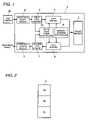
- FIG. 1is a block diagram showing a scan converter in accordance with a first embodiment of the present invention.
- FIG. 2is a view showing address areas of a frame memory in the scan converter.
- FIGS. 3 and 4are timing charts showing timing for switching between the address areas in the scan converter.
- FIG. 5is a timing chart showing timing for switching between a write enable signal and a read enable signal in the scan converter.
- FIG. 6is a timing chart showing timing for transmitting data between the first and second FIFO memories and the frame memory in the scan converter.
- FIG. 7is a timing chart showing refreshing timing of the frame memory in the scan converter.
- FIG. 8is a timing chart showing another timing for switching between the address areas in the scan converter.
- FIG. 9is a block diagram showing a scan converter in accordance with a second embodiment of the present invention.
- FIG. 10is a timing chart showing timing for transmitting data between the first and second FIFO memories and the frame memory in the scan converter of the FIG. 9 .
- FIG. 11is a timing chart showing timing for switching between a write enable signal and a read enable signal in the scan converter of the FIG. 9 .
- FIG. 1is a block diagram of a scan converter in accordance with a first embodiment of the present invention.
- the scan converter 1takes a progressive scan video data from a CCD camera 20 and outputs an interlaced scan video data based on the standard television signal (NTSC, PAL, or SECAM).
- the CCD camera 20outputs video data in progressive scan mode at a first transfer rate which is determined by a clock signal supplied to the CCD camera 20 or a signal obtained by dividing the clock signal.
- the first transfer rateis faster than a transfer rate (a third transfer rate) which is based on the standard television signal.
- the scan converter 1comprises a video data input circuit 2 , a first FIFO memory 3 , a data writer 4 , a frame memory 5 , a data reader 6 , a second FIFO memory 7 , a video data output circuit 8 , a memory address controller 9 , and a write/read timing controller 10 .
- the video data input circuit 2takes the video data from the CCD camera 20 and writes the video data into the first FIFO memory 3 at the first transfer rate.
- the first FIFO memory 3has a data storage capacity of 24 words (in other words, the first FIFO memory 3 can hold 24 pixels of the video data), and when it stores 8 or more words of the video data, it outputs a write request signal to the write/read timing controller 10 .
- the second FIFO memory 7also has a data storage capacity of 24 words. When it has available space of 8 or more words, it outputs a read request signal to the write/read timing controller 10 .
- the data writer 4transfers the video data from the first FIFO memory 3 to the frame memory 5 , as described later in detail.
- the data reader 6transfers the video data from the frame memory 5 to the second FIFO memory 7 , as described later in detail.
- the frame memory 5is SDRAM (synchronous Dynamic Random Access Memory), which has a single input/output port.
- the frame memory 5has a data storage capacity of 3 frames.
- the frame memory 5has a write period in which the frame memory is writable and a read period in which the frame memory is readable. Data transmission between the first or second FIFO memory and the frame memory 5 is accomplished in 8 words burst mode.
- the frame memory 5is divided into three address areas 5 a , 5 b , and 5 c , each of which has a data storage capacity of one frame.
- the memory address controller 9controls an address of the frame memory 5 in which the data writer 4 writes the video data and an address of the frame memory 5 from which the data reader 6 reads out the video data. More specifically, the memory address controller 9 allocates one of the address areas 5 a , 5 b , and 5 c to a write address area in which the data writer 4 writes the video data, and it allocates one of the address areas which is different from the write address area to a read address area from which the data reader 6 reads out the video data. As shown in FIG.
- the memory address controller 9switches the write address area in the order of 5 a - 5 b - 5 c in synchronization with one frame of the vertical synchronizing signal (VSYNC) of the video data sent from the CCD camera 20 . And, the memory address controller 9 switches the read address area in synchronization with one frame of the vertical synchronizing signal of the standard television signal generated by the video data output circuit 8 (as is well known, one frame of the standard television signal is composed of two fields; even-field and odd field.). The memory address controller 9 allocates one of the address area which was allocated to the write address area immediately preceding the current write address area to the read address area. For example, at time t 1 in FIG.
- the memory address controller 9allocates the address areas 5 c , which was allocated to the write address area immediately preceding the current write address area 5 a , to the read address area. Similarly, at time t 2 , the memory address controller 9 allocates the address areas 5 a , which was allocated to the write address area immediately preceding the current write address area 5 b , to the read address area.
- FIG. 4shows a case where the interval of the one frame of the video data sent from the CCD camera 20 becomes longer than the interval of the one frame of the standard television signal because of a function, such as a slow shutter, of the CCD camera 20 .
- the memory address controller 9allocates the address areas 5 c to the read address area, and, at time t 4 , too, the memory address controller 9 allocates the address areas 5 c to the read address area, because, at time t 4 , in comparison with the time t 3 , the address area which was allocated to the write address area immediately preceding the current write address area ( 5 a ) dose not change.
- the write/read timing controller 10alternately generates a write enable signal which sets the frame memory 5 in the write period and a read enable signal which sets the frame memory 5 in the read period.
- the write enable signalis held high during a period needed for transmitting 8 words from the first FIFO memory 3 to the frame memory 5 . More specifically, as shown in FIG. 5 , the write enable signal is held high while an “ACT” command and a row address (“ROW”) are inputted into the frame memory 5 to activate the frame memory 5 and then a “WRITEA” command and a column address (“COL”) are inputted into the frame memory 5 and then 8 words video data are written into the frame memory 5 and a pre-charge of the frame memory 5 is performed (“Trp”).
- the “ACT” commandis a command which switches the frame memory 5 from a standby state to an active state
- the “WRITEA” commandis a command to write data in an address specified by the row address and the column address.
- a “Trcd”shows a time period which is needed for performing the “WRITEA” command after performing the “ACT” command.
- the pre-chargeis performed automatically at regular time intervals (“Ts”).
- the read enable signalis held high during a period needed for transmitting 8 words from the frame memory 5 to the second FIFO memory 7 . More specifically, as shown in FIG. 5 , the read enable signal is held high while the “ACT” command and a row address (“ROW”) is inputted into the frame memory 5 and then a “READA” command and a column address (“COL”) is inputted into the frame memory 5 and then 8 words video data are read out from the frame memory 5 and the pre-charge is performed.
- the “READA” commandis a command to read out data from specified address.
- “Tcl”shows a time period which is needed for reading out data from specified address after performing the “READA” command.
- the write enable signal and the read enable signalare switched in a period shorter than the period of the horizontal synchronizing signal (HSYNC) of the standard television signal.
- the data writer 4receives the write enable signal from the write/read timing controller 10 and receives the write request signal from the first FIFO memory 3 . And, as shown in FIG. 6 , while the write request signal is high, the data writer 4 transfers 8 words in burst mode from the first FIFO memory 3 to the frame memory 5 in response to the rising edge of the write enable signal. That is, the video data is written into the frame memory 5 when the first FIFO memory 3 stores 8 or more words of the video data and the frame memory 5 has been set in the writable period.
- the transfer rate (a second transfer rate) from the first FIFO memory 3 to the frame memory 5is set twice as fast as the first transfer rate.
- the data reader 6receives the read enable signal from the write/read timing controller 10 and receives the read request signal from the second FIFO memory 7 . And, as shown in FIG. 6 , while the read request signal is high, the data reader 6 transfers 8 words in burst mode from the frame memory 5 to the second FIFO memory 7 in response to the rising edge of the read enable signal. At that time, the data reader 6 reads out the video data from the frame memory 5 in interlaced scan mode. That is, the video data is read out from the frame memory 5 when the second FIFO memory 7 has available space of 8 or more words and the frame memory 5 has been set in the readable period.
- the transfer rate from the frame memory 5 to the second FIFO memory 7is also set twice as fast as the first transfer rate; that is, the second transfer rate.
- the switching timing between the write enable signal and the read enable signalis not synchronized with the write request signal and the read request signal (In other words, the switching timing between the write enable signal and the read enable signal is not synchronized with the timing that the video input means 2 writes the video data into the first FIFO memory 3 and the timing that the video data output circuit 8 reads out the video data from the second FIFO memory 7 .).
- the video data output circuit 8reads out the video data from the second FIFO memory 7 based on the timing and the clock (the third transfer rate) of the standard television signal and generates a television signal to output the interlaced scan video data.
- the scan converter 1configured as mentioned above can stably convert the progressive scan video data into the interlaced scan video data using a single port type frame memory 5 even if the progressive scan video data and the interlaced scan video data do not synchronized each other. The reason will be described below.
- the video data written into the first FIFO memory 3 during one pair of the write period and the read periodcan be all transmitted to the frame memory 5 during the pair of the write period and the read period if the second transfer rate r 2 is at least twice as fast as the first transfer rate r 1 . That is, the video data does not keep increasing in the first FIFO memory 3 if the second transfer rate r 2 is at least twice as fast as the first transfer rate r 1 .
- the video data written into the second FIFO memory 7 during one pair of the write period and the read periodcan not be less than zero in the second FIFO memory 7 . That is, the video data is outputted continuously from the second FIFO memory 7 , without interruption.
- the third transfer ratemay be faster than the first transfer rate.
- the second transfer rate r 2is at least twice as fast as the third transfer rate r 3 . That is, it is necessary that the second transfer rate is at least twice as fast as the first transfer rate or the third transfer rate, whichever is faster.
- the time period T of each write periodis preferred to be short in order to reduce the data storage capacity of the first FIFO memory.
- the time period T of each read periodis preferred to be short. So, in this embodiment, the write/read timing controller 10 switches between the write enable signal and the read enable signal in a period shorter than the period of the horizontal synchronizing signal (HSYNC) of the standard television signal to reduce the data storage capacity of the first and second FIFO memories.
- the scan convertercan more stably convert the progressive scan video data into the interlaced scan video data.
- the scan converter 1can output the video data without interruption even if a frame rate of the video data from the CCD camera 20 becomes slow because of a function, such as a slow shutter, of the CCD camera 20 .
- the frame memory 5requires refreshing. It is preferable that the frame memory 5 is refreshed in a blanking period of the video data read out from the frame memory 5 .
- the frame memory 5is refreshed by using “PALL” command and “REF” command in response to the rising edge of the read enable signal while the horizontal synchronizing signal (HSYNC) of the standard television signal generated by the video data output circuit 8 is LOW, that is, in the blanking period of the video data.
- the “PALL” commandis a command which performs pre-charge of the frame memory 5 and the “REF” command is a command which performs auto-refreshing.
- a “Trc”shows a time period which is needed for performing a command after performing the “REF” command. Therefore, even if the video data is outputted from the scan converter 1 at a slow frame rate because of a function such as a slow shutter, it is prevented that the frame memory 5 loses the data by volatilization.
- the memory address controller 9switches the read address area in synchronization with one frame of the vertical synchronizing signal of the standard television signal generated by the video data output circuit 8
- the memory address controller 9may switch the read address area in synchronization with one field of the vertical synchronizing signal of the standard television signal, as shown in FIG. 8 .
- the read address areamay be switched in synchronization with each field of the interlaced scan video data.
- the memory address controller 9allocates the address areas which was allocated to the write address area immediately preceding the current write address area, to the read address area.
- the scan converter 1can output fast-moving video data smoothly.
- FIG. 9shows a scan converter 100 in accordance with a second embodiment of the present invention.
- the basic composition of this embodimentis identical to the first embodiment, so the similar part of these embodiments are identified by the same reference character and no duplicate explanation is made here.
- the first transfer rateis faster than the third transfer rate.
- This scan converter 100includes an arithmetic processing circuit 11 which performs computations, such as resizing, filtering, and zooming of an image, in addition to the composition of the first embodiment.
- the second FIFO memory 7 in this embodimenthas a data storage capacity of 24 words, and when it has available space of 16 or more words, it outputs a read request signal to the write/read timing controller 10 .
- the write enable signalis held high during a period needed for transmitting 8 words from the first FIFO memory 3 to the frame memory 5
- the read enable signalis held high during a period needed for transmitting 8 words twice from the frame memory 5 to the second FIFO memory 7 . That is, as shown in FIG. 11 , the read enable signal is held high while the predetermined sequence for transmitting 8 words; inputting “ACT” command and a “READA” command and transmitting 8 words video data and performing the pre-charge, is performed twice.
- the data writer 4transfers 8 words in burst mode from the first FIFO memory 3 to the frame memory 5 in response to the rising edge of the write enable signal while the write request signal is high.
- the transfer rate (the second transfer rate) from the first FIFO memory 3 to the frame memory 5is set three times as fast as the first transfer rate.
- the data reader 6transfers 8 words twice in burst mode from the frame memory 5 to the second FIFO memory 7 in response to the rising edge of the read enable signal while the read request signal is high. At that time, the data reader 6 reads out 8 words (pixels) video data, which are consecutive 8 pixels in horizontal direction and not greater than one line, as the first video data from the frame memory 5 , and furthermore, it reads out 8 words (pixels) video data which are adjacent to the first video data in a vertical direction as the second video data from the frame memory 5 .
- the transfer rate from the frame memory 5 to the second FIFO memory 7is also set three times as fast as the first transfer rate.
- the switching timing between the write enable signal and the read enable signalis not synchronized with the write request signal and the read request signal.
- the first video data stored in the second FIFO memory 7is outputted from the video data output circuit 8 to the exterior at the third transfer rate based on the standard television signal. Furthermore, using the first and second video data stored in the second FIFO memory 7 , the arithmetic processing circuit 11 performs various computations, such as horizontal/vertical compression of the video data, and then, the arithmetic processing circuit 11 outputs the result of the computations to the video data output circuit 8 . By including the arithmetic processing circuit 11 , the scan converter 100 of this embodiment can performs resizing, filtering, zooming of an image and so on, easily, without extra line memory.
- the scan converter 100can stably convert the progressive scan video data into the interlaced scan video data, without an overflow of the video data sent from the CCD camera 20 and an interruption of the video data to be outputted from the scan converter 100 .
Landscapes
- Engineering & Computer Science (AREA)
- Computer Graphics (AREA)
- Multimedia (AREA)
- Signal Processing (AREA)
- Television Systems (AREA)
Abstract
Description
D1=2*T*r1
where T is a time period of each write period and each read period, and r1 is the first transfer rate.
D2=T*r2
where r2 is the second transfer rate, because the video data can be transmitted from the
D3=D1−D2=2*T*r1−T*r2
D3<=0
D4=T*r2
where T is the time period of each read period and r2 is the second transfer rate, as mentioned above.
D5=2*T*r3
where r3 is the third transfer rate, that is, the transfer rate of the standard television signal.
D6=D4−D5=T*r2−2*T*r3
D6>=0
Claims (8)
Applications Claiming Priority (2)
| Application Number | Priority Date | Filing Date | Title |
|---|---|---|---|
| JP2004-162352 | 2004-05-31 | ||
| JP2004162352AJP4306536B2 (en) | 2004-05-31 | 2004-05-31 | Scan converter |
Publications (2)
| Publication Number | Publication Date |
|---|---|
| US20050264691A1 US20050264691A1 (en) | 2005-12-01 |
| US7349027B2true US7349027B2 (en) | 2008-03-25 |
Family
ID=34934643
Family Applications (1)
| Application Number | Title | Priority Date | Filing Date |
|---|---|---|---|
| US11/094,157Expired - Fee RelatedUS7349027B2 (en) | 2004-05-31 | 2005-03-31 | Scan converter |
Country Status (4)
| Country | Link |
|---|---|
| US (1) | US7349027B2 (en) |
| EP (1) | EP1603332B1 (en) |
| JP (1) | JP4306536B2 (en) |
| CN (1) | CN100344157C (en) |
Cited By (17)
| Publication number | Priority date | Publication date | Assignee | Title |
|---|---|---|---|---|
| US20060132651A1 (en)* | 2004-12-20 | 2006-06-22 | Nec Electronics Corporation | Frame synchronizer, optical disk device, information recording/reproducing apparatus, and signal synchronizing method |
| US20060132647A1 (en)* | 2004-12-22 | 2006-06-22 | Ming-Jane Hsieh | Method and apparatus for simultaneous display in progressive and interlaced scanning modes |
| US20140098228A1 (en)* | 2005-12-08 | 2014-04-10 | Smart Drive Systems, Inc. | Memory management in event recording systems |
| US8868288B2 (en) | 2006-11-09 | 2014-10-21 | Smartdrive Systems, Inc. | Vehicle exception event management systems |
| US8892310B1 (en) | 2014-02-21 | 2014-11-18 | Smartdrive Systems, Inc. | System and method to detect execution of driving maneuvers |
| US8989959B2 (en) | 2006-11-07 | 2015-03-24 | Smartdrive Systems, Inc. | Vehicle operator performance history recording, scoring and reporting systems |
| US9183679B2 (en) | 2007-05-08 | 2015-11-10 | Smartdrive Systems, Inc. | Distributed vehicle event recorder systems having a portable memory data transfer system |
| US9201842B2 (en) | 2006-03-16 | 2015-12-01 | Smartdrive Systems, Inc. | Vehicle event recorder systems and networks having integrated cellular wireless communications systems |
| US9402060B2 (en) | 2006-03-16 | 2016-07-26 | Smartdrive Systems, Inc. | Vehicle event recorders with integrated web server |
| US9501878B2 (en) | 2013-10-16 | 2016-11-22 | Smartdrive Systems, Inc. | Vehicle event playback apparatus and methods |
| US9554080B2 (en) | 2006-11-07 | 2017-01-24 | Smartdrive Systems, Inc. | Power management systems for automotive video event recorders |
| US9610955B2 (en) | 2013-11-11 | 2017-04-04 | Smartdrive Systems, Inc. | Vehicle fuel consumption monitor and feedback systems |
| US9633318B2 (en) | 2005-12-08 | 2017-04-25 | Smartdrive Systems, Inc. | Vehicle event recorder systems |
| US9663127B2 (en) | 2014-10-28 | 2017-05-30 | Smartdrive Systems, Inc. | Rail vehicle event detection and recording system |
| US9728228B2 (en) | 2012-08-10 | 2017-08-08 | Smartdrive Systems, Inc. | Vehicle event playback apparatus and methods |
| US10930093B2 (en) | 2015-04-01 | 2021-02-23 | Smartdrive Systems, Inc. | Vehicle event recording system and method |
| US11069257B2 (en) | 2014-11-13 | 2021-07-20 | Smartdrive Systems, Inc. | System and method for detecting a vehicle event and generating review criteria |
Families Citing this family (11)
| Publication number | Priority date | Publication date | Assignee | Title |
|---|---|---|---|---|
| JP5360589B2 (en)* | 2009-12-14 | 2013-12-04 | 株式会社リコー | Imaging device |
| US8624999B2 (en)* | 2009-12-01 | 2014-01-07 | Ricoh Company, Ltd. | Imaging apparatus |
| JP2011139432A (en)* | 2009-12-01 | 2011-07-14 | Ricoh Co Ltd | Imaging apparatus |
| JP2013168097A (en)* | 2012-02-17 | 2013-08-29 | Japan Display West Co Ltd | Display apparatus and display method |
| JP2013219598A (en)* | 2012-04-10 | 2013-10-24 | Canon Inc | Transmission device and transmission method |
| CN104469241B (en)* | 2014-11-28 | 2018-01-16 | 中国航空无线电电子研究所 | A kind of device for realizing video frame rate conversion |
| JP7102269B2 (en)* | 2018-07-11 | 2022-07-19 | キヤノン株式会社 | Image processing device, control method of image processing device, and program |
| JP7011373B2 (en)* | 2018-07-11 | 2022-01-26 | キヤノン株式会社 | Multifunction device and its control method, and program |
| CN111710282B (en)* | 2020-07-02 | 2023-04-07 | 硅谷数模(苏州)半导体股份有限公司 | Control method and control device of time schedule controller and data transmission system |
| KR102857440B1 (en) | 2021-12-31 | 2025-09-09 | 엘지디스플레이 주식회사 | Data Communication circuit and Display Device including the same |
| US12314161B2 (en)* | 2022-04-22 | 2025-05-27 | Chongqing Boe Optoelectronics Technology Co., Ltd. | Method and apparatus for controlling read timing, and computer-readable storage medium |
Citations (21)
| Publication number | Priority date | Publication date | Assignee | Title |
|---|---|---|---|---|
| US5767903A (en) | 1995-01-13 | 1998-06-16 | Nec Corporation | Solid-state image pickup device operable at a frame rate with a controllable accumulating time interval |
| US5949950A (en)* | 1992-08-31 | 1999-09-07 | Canon Kabushiki Kaisha | Apparatus for recording picked up image signal on second memory through first memory |
| US6226038B1 (en)* | 1998-04-03 | 2001-05-01 | Avid Technology, Inc. | HDTV editing and effects previsualization using SDTV devices |
| US6337716B1 (en)* | 1998-12-09 | 2002-01-08 | Samsung Electronics Co., Ltd. | Receiver for simultaneously displaying signals having different display formats and/or different frame rates and method thereof |
| US6356306B1 (en) | 1997-02-28 | 2002-03-12 | Sanyo Electric Co., Ltd. | Digital camera capable of converting a progressive scan signal into an interlace scan signal |
| US20020109698A1 (en)* | 2001-02-15 | 2002-08-15 | Mark Champion | Checkerboard buffer using memory blocks |
| US20020109792A1 (en)* | 2001-02-15 | 2002-08-15 | Mark Champion | Two-dimensional buffer pages using memory bank alternation |
| US20020109791A1 (en)* | 2001-02-15 | 2002-08-15 | Mark Champion | Two-dimensional buffer pages |
| US20020113904A1 (en)* | 2001-02-15 | 2002-08-22 | Mark Champion | Two-dimensional buffer pages using bit-field addressing |
| JP3363761B2 (en) | 1997-11-26 | 2003-01-08 | 三洋電機株式会社 | Signal conversion circuit |
| US6538700B1 (en)* | 1999-06-25 | 2003-03-25 | Sony Corporation | Synchronizing conversion apparatus and method as well as recording medium |
| US6567130B1 (en)* | 2000-03-30 | 2003-05-20 | Sencore, Inc. | Method and apparatus for capturing video files for use in HDTV broadcast and demonstration |
| US6570579B1 (en)* | 1998-11-09 | 2003-05-27 | Broadcom Corporation | Graphics display system |
| US20030184678A1 (en)* | 2002-04-01 | 2003-10-02 | Jiunn-Kuang Chen | Display controller provided with dynamic output clock |
| US6636269B1 (en)* | 1999-08-18 | 2003-10-21 | Webtv Networks, Inc. | Video timing system and method |
| US6798420B1 (en)* | 1998-11-09 | 2004-09-28 | Broadcom Corporation | Video and graphics system with a single-port RAM |
| US20050104890A1 (en)* | 2001-02-15 | 2005-05-19 | Sony Corporation | Dynamic buffer pages |
| US6922195B2 (en)* | 2002-07-30 | 2005-07-26 | Oki Electric Industry Co., Ltd. | Image processing apparatus |
| US6950144B2 (en)* | 2001-02-15 | 2005-09-27 | Samsung Electronics Co., Ltd. | Apparatus and method of controlling image display |
| US7136110B2 (en)* | 2000-06-14 | 2006-11-14 | Canon Kabushiki Kaisha | Image signal processing apparatus |
| US7142252B2 (en)* | 2001-03-10 | 2006-11-28 | Samsung Electronics Co., Ltd. | Image processing apparatus and method for displaying picture-in-picture with frame rate conversion |
Family Cites Families (4)
| Publication number | Priority date | Publication date | Assignee | Title |
|---|---|---|---|---|
| CN1003274B (en)* | 1984-10-03 | 1989-02-08 | 三洋电机株式会社 | Scan conversion method and scan conversion device using the same |
| KR100326919B1 (en)* | 1999-08-23 | 2002-03-13 | 윤종용 | apparatus and method for down-converting |
| CN2457822Y (en)* | 2001-01-04 | 2001-10-31 | 中国科学院长春光学精密机械与物理研究所 | Adaptor for conversing line-by-line video frequency to interlacing standard video frequency signal |
| US6847405B2 (en)* | 2001-09-14 | 2005-01-25 | Sony Corporation | Motion-adaptive de-interlacing method and system for digital televisions |
- 2004
- 2004-05-31JPJP2004162352Apatent/JP4306536B2/ennot_activeExpired - Fee Related
- 2005
- 2005-03-31EPEP05007068Apatent/EP1603332B1/ennot_activeExpired - Lifetime
- 2005-03-31USUS11/094,157patent/US7349027B2/ennot_activeExpired - Fee Related
- 2005-05-20CNCNB2005100737127Apatent/CN100344157C/ennot_activeExpired - Fee Related
Patent Citations (22)
| Publication number | Priority date | Publication date | Assignee | Title |
|---|---|---|---|---|
| US5949950A (en)* | 1992-08-31 | 1999-09-07 | Canon Kabushiki Kaisha | Apparatus for recording picked up image signal on second memory through first memory |
| US5767903A (en) | 1995-01-13 | 1998-06-16 | Nec Corporation | Solid-state image pickup device operable at a frame rate with a controllable accumulating time interval |
| US6356306B1 (en) | 1997-02-28 | 2002-03-12 | Sanyo Electric Co., Ltd. | Digital camera capable of converting a progressive scan signal into an interlace scan signal |
| JP3363761B2 (en) | 1997-11-26 | 2003-01-08 | 三洋電機株式会社 | Signal conversion circuit |
| US6226038B1 (en)* | 1998-04-03 | 2001-05-01 | Avid Technology, Inc. | HDTV editing and effects previsualization using SDTV devices |
| US20050024369A1 (en)* | 1998-11-09 | 2005-02-03 | Broadcom Corporation | Video and graphics system with a single-port RAM |
| US6798420B1 (en)* | 1998-11-09 | 2004-09-28 | Broadcom Corporation | Video and graphics system with a single-port RAM |
| US6570579B1 (en)* | 1998-11-09 | 2003-05-27 | Broadcom Corporation | Graphics display system |
| US6337716B1 (en)* | 1998-12-09 | 2002-01-08 | Samsung Electronics Co., Ltd. | Receiver for simultaneously displaying signals having different display formats and/or different frame rates and method thereof |
| US6538700B1 (en)* | 1999-06-25 | 2003-03-25 | Sony Corporation | Synchronizing conversion apparatus and method as well as recording medium |
| US6636269B1 (en)* | 1999-08-18 | 2003-10-21 | Webtv Networks, Inc. | Video timing system and method |
| US6567130B1 (en)* | 2000-03-30 | 2003-05-20 | Sencore, Inc. | Method and apparatus for capturing video files for use in HDTV broadcast and demonstration |
| US7136110B2 (en)* | 2000-06-14 | 2006-11-14 | Canon Kabushiki Kaisha | Image signal processing apparatus |
| US20020113904A1 (en)* | 2001-02-15 | 2002-08-22 | Mark Champion | Two-dimensional buffer pages using bit-field addressing |
| US20020109791A1 (en)* | 2001-02-15 | 2002-08-15 | Mark Champion | Two-dimensional buffer pages |
| US20020109792A1 (en)* | 2001-02-15 | 2002-08-15 | Mark Champion | Two-dimensional buffer pages using memory bank alternation |
| US20020109698A1 (en)* | 2001-02-15 | 2002-08-15 | Mark Champion | Checkerboard buffer using memory blocks |
| US20050104890A1 (en)* | 2001-02-15 | 2005-05-19 | Sony Corporation | Dynamic buffer pages |
| US6950144B2 (en)* | 2001-02-15 | 2005-09-27 | Samsung Electronics Co., Ltd. | Apparatus and method of controlling image display |
| US7142252B2 (en)* | 2001-03-10 | 2006-11-28 | Samsung Electronics Co., Ltd. | Image processing apparatus and method for displaying picture-in-picture with frame rate conversion |
| US20030184678A1 (en)* | 2002-04-01 | 2003-10-02 | Jiunn-Kuang Chen | Display controller provided with dynamic output clock |
| US6922195B2 (en)* | 2002-07-30 | 2005-07-26 | Oki Electric Industry Co., Ltd. | Image processing apparatus |
Non-Patent Citations (1)
| Title |
|---|
| European Search Report dated Sep. 27, 2006. |
Cited By (44)
| Publication number | Priority date | Publication date | Assignee | Title |
|---|---|---|---|---|
| US20060132651A1 (en)* | 2004-12-20 | 2006-06-22 | Nec Electronics Corporation | Frame synchronizer, optical disk device, information recording/reproducing apparatus, and signal synchronizing method |
| US20060132647A1 (en)* | 2004-12-22 | 2006-06-22 | Ming-Jane Hsieh | Method and apparatus for simultaneous display in progressive and interlaced scanning modes |
| US9226004B1 (en) | 2005-12-08 | 2015-12-29 | Smartdrive Systems, Inc. | Memory management in event recording systems |
| US20140098228A1 (en)* | 2005-12-08 | 2014-04-10 | Smart Drive Systems, Inc. | Memory management in event recording systems |
| US10878646B2 (en) | 2005-12-08 | 2020-12-29 | Smartdrive Systems, Inc. | Vehicle event recorder systems |
| US8880279B2 (en)* | 2005-12-08 | 2014-11-04 | Smartdrive Systems, Inc. | Memory management in event recording systems |
| US9633318B2 (en) | 2005-12-08 | 2017-04-25 | Smartdrive Systems, Inc. | Vehicle event recorder systems |
| US9691195B2 (en) | 2006-03-16 | 2017-06-27 | Smartdrive Systems, Inc. | Vehicle event recorder systems and networks having integrated cellular wireless communications systems |
| US9545881B2 (en) | 2006-03-16 | 2017-01-17 | Smartdrive Systems, Inc. | Vehicle event recorder systems and networks having integrated cellular wireless communications systems |
| US9208129B2 (en) | 2006-03-16 | 2015-12-08 | Smartdrive Systems, Inc. | Vehicle event recorder systems and networks having integrated cellular wireless communications systems |
| US9942526B2 (en) | 2006-03-16 | 2018-04-10 | Smartdrive Systems, Inc. | Vehicle event recorders with integrated web server |
| US9402060B2 (en) | 2006-03-16 | 2016-07-26 | Smartdrive Systems, Inc. | Vehicle event recorders with integrated web server |
| US9472029B2 (en) | 2006-03-16 | 2016-10-18 | Smartdrive Systems, Inc. | Vehicle event recorder systems and networks having integrated cellular wireless communications systems |
| US9201842B2 (en) | 2006-03-16 | 2015-12-01 | Smartdrive Systems, Inc. | Vehicle event recorder systems and networks having integrated cellular wireless communications systems |
| US10404951B2 (en) | 2006-03-16 | 2019-09-03 | Smartdrive Systems, Inc. | Vehicle event recorders with integrated web server |
| US9566910B2 (en) | 2006-03-16 | 2017-02-14 | Smartdrive Systems, Inc. | Vehicle event recorder systems and networks having integrated cellular wireless communications systems |
| US9554080B2 (en) | 2006-11-07 | 2017-01-24 | Smartdrive Systems, Inc. | Power management systems for automotive video event recorders |
| US9761067B2 (en) | 2006-11-07 | 2017-09-12 | Smartdrive Systems, Inc. | Vehicle operator performance history recording, scoring and reporting systems |
| US10339732B2 (en) | 2006-11-07 | 2019-07-02 | Smartdrive Systems, Inc. | Vehicle operator performance history recording, scoring and reporting systems |
| US8989959B2 (en) | 2006-11-07 | 2015-03-24 | Smartdrive Systems, Inc. | Vehicle operator performance history recording, scoring and reporting systems |
| US10682969B2 (en) | 2006-11-07 | 2020-06-16 | Smartdrive Systems, Inc. | Power management systems for automotive video event recorders |
| US10053032B2 (en) | 2006-11-07 | 2018-08-21 | Smartdrive Systems, Inc. | Power management systems for automotive video event recorders |
| US11623517B2 (en) | 2006-11-09 | 2023-04-11 | SmartDriven Systems, Inc. | Vehicle exception event management systems |
| US9738156B2 (en) | 2006-11-09 | 2017-08-22 | Smartdrive Systems, Inc. | Vehicle exception event management systems |
| US10471828B2 (en) | 2006-11-09 | 2019-11-12 | Smartdrive Systems, Inc. | Vehicle exception event management systems |
| US8868288B2 (en) | 2006-11-09 | 2014-10-21 | Smartdrive Systems, Inc. | Vehicle exception event management systems |
| US9679424B2 (en) | 2007-05-08 | 2017-06-13 | Smartdrive Systems, Inc. | Distributed vehicle event recorder systems having a portable memory data transfer system |
| US9183679B2 (en) | 2007-05-08 | 2015-11-10 | Smartdrive Systems, Inc. | Distributed vehicle event recorder systems having a portable memory data transfer system |
| US9728228B2 (en) | 2012-08-10 | 2017-08-08 | Smartdrive Systems, Inc. | Vehicle event playback apparatus and methods |
| US10818112B2 (en) | 2013-10-16 | 2020-10-27 | Smartdrive Systems, Inc. | Vehicle event playback apparatus and methods |
| US10019858B2 (en) | 2013-10-16 | 2018-07-10 | Smartdrive Systems, Inc. | Vehicle event playback apparatus and methods |
| US9501878B2 (en) | 2013-10-16 | 2016-11-22 | Smartdrive Systems, Inc. | Vehicle event playback apparatus and methods |
| US9610955B2 (en) | 2013-11-11 | 2017-04-04 | Smartdrive Systems, Inc. | Vehicle fuel consumption monitor and feedback systems |
| US11884255B2 (en) | 2013-11-11 | 2024-01-30 | Smartdrive Systems, Inc. | Vehicle fuel consumption monitor and feedback systems |
| US11260878B2 (en) | 2013-11-11 | 2022-03-01 | Smartdrive Systems, Inc. | Vehicle fuel consumption monitor and feedback systems |
| US9594371B1 (en) | 2014-02-21 | 2017-03-14 | Smartdrive Systems, Inc. | System and method to detect execution of driving maneuvers |
| US10249105B2 (en) | 2014-02-21 | 2019-04-02 | Smartdrive Systems, Inc. | System and method to detect execution of driving maneuvers |
| US11250649B2 (en) | 2014-02-21 | 2022-02-15 | Smartdrive Systems, Inc. | System and method to detect execution of driving maneuvers |
| US10497187B2 (en) | 2014-02-21 | 2019-12-03 | Smartdrive Systems, Inc. | System and method to detect execution of driving maneuvers |
| US11734964B2 (en) | 2014-02-21 | 2023-08-22 | Smartdrive Systems, Inc. | System and method to detect execution of driving maneuvers |
| US8892310B1 (en) | 2014-02-21 | 2014-11-18 | Smartdrive Systems, Inc. | System and method to detect execution of driving maneuvers |
| US9663127B2 (en) | 2014-10-28 | 2017-05-30 | Smartdrive Systems, Inc. | Rail vehicle event detection and recording system |
| US11069257B2 (en) | 2014-11-13 | 2021-07-20 | Smartdrive Systems, Inc. | System and method for detecting a vehicle event and generating review criteria |
| US10930093B2 (en) | 2015-04-01 | 2021-02-23 | Smartdrive Systems, Inc. | Vehicle event recording system and method |
Also Published As
| Publication number | Publication date |
|---|---|
| CN1705368A (en) | 2005-12-07 |
| JP2005347874A (en) | 2005-12-15 |
| EP1603332A2 (en) | 2005-12-07 |
| JP4306536B2 (en) | 2009-08-05 |
| EP1603332B1 (en) | 2011-08-24 |
| EP1603332A3 (en) | 2006-10-25 |
| CN100344157C (en) | 2007-10-17 |
| US20050264691A1 (en) | 2005-12-01 |
Similar Documents
| Publication | Publication Date | Title |
|---|---|---|
| US7349027B2 (en) | Scan converter | |
| JPH08305860A (en) | Image decoding display device | |
| KR100194922B1 (en) | Aspect ratio inverter | |
| US20050062860A1 (en) | Frame memory device and method | |
| US4797743A (en) | Video memory control device | |
| KR101128167B1 (en) | Image display device | |
| US7209186B2 (en) | Image processing apparatus and image processing method for high speed real-time processing | |
| US20080136966A1 (en) | Frame Synchronizer, Synchronization Method of Frame Synchronizer, Image Processing Apparatus, and Frame Synchronization Program | |
| JP4735475B2 (en) | Moving image processing method and moving image processing apparatus | |
| KR100331797B1 (en) | Apparatus for memory controlling of digital TV | |
| JPH1013841A (en) | Method and device for decoding picture | |
| JP2000284771A (en) | Video data processing device | |
| JPH09200784A (en) | Imaging device | |
| JP3601748B2 (en) | Color imaging apparatus and digital component signal generation method | |
| JPH0423993B2 (en) | ||
| JPH05308544A (en) | Video signal processor | |
| KR19980073567A (en) | Closed circuit television systems | |
| JP2622622B2 (en) | Scan line number conversion control method | |
| KR0141303B1 (en) | Still Image Selector of Video Decoder | |
| JPS6327504Y2 (en) | ||
| KR100620930B1 (en) | Image signal processing circuit | |
| JPH03207177A (en) | Reduced picture display device | |
| JPH0515348B2 (en) | ||
| JP2005079848A (en) | Sequential scanning line converter and video signal processing system | |
| JP2019134437A (en) | Imaging apparatus, method for controlling the same, and program |
Legal Events
| Date | Code | Title | Description |
|---|---|---|---|
| AS | Assignment | Owner name:MATSUSHITA ELECTRIC WORKS, LTD., JAPAN Free format text:ASSIGNMENT OF ASSIGNORS INTEREST;ASSIGNORS:ENDO, JUNPEI;FURUKAWA, SATOSHI;HAGIO, KENICHI;REEL/FRAME:016447/0171 Effective date:20050318 | |
| FEPP | Fee payment procedure | Free format text:PAYOR NUMBER ASSIGNED (ORIGINAL EVENT CODE: ASPN); ENTITY STATUS OF PATENT OWNER: LARGE ENTITY | |
| STCF | Information on status: patent grant | Free format text:PATENTED CASE | |
| AS | Assignment | Owner name:PANASONIC ELECTRIC WORKS CO., LTD., JAPAN Free format text:CHANGE OF NAME;ASSIGNOR:MATSUSHITA ELECTRIC WORKS, LTD.;REEL/FRAME:022191/0478 Effective date:20081001 Owner name:PANASONIC ELECTRIC WORKS CO., LTD.,JAPAN Free format text:CHANGE OF NAME;ASSIGNOR:MATSUSHITA ELECTRIC WORKS, LTD.;REEL/FRAME:022191/0478 Effective date:20081001 | |
| FPAY | Fee payment | Year of fee payment:4 | |
| FEPP | Fee payment procedure | Free format text:PAYOR NUMBER ASSIGNED (ORIGINAL EVENT CODE: ASPN); ENTITY STATUS OF PATENT OWNER: LARGE ENTITY Free format text:PAYER NUMBER DE-ASSIGNED (ORIGINAL EVENT CODE: RMPN); ENTITY STATUS OF PATENT OWNER: LARGE ENTITY | |
| FPAY | Fee payment | Year of fee payment:8 | |
| FEPP | Fee payment procedure | Free format text:MAINTENANCE FEE REMINDER MAILED (ORIGINAL EVENT CODE: REM.); ENTITY STATUS OF PATENT OWNER: LARGE ENTITY | |
| LAPS | Lapse for failure to pay maintenance fees | Free format text:PATENT EXPIRED FOR FAILURE TO PAY MAINTENANCE FEES (ORIGINAL EVENT CODE: EXP.); ENTITY STATUS OF PATENT OWNER: LARGE ENTITY | |
| STCH | Information on status: patent discontinuation | Free format text:PATENT EXPIRED DUE TO NONPAYMENT OF MAINTENANCE FEES UNDER 37 CFR 1.362 | |
| FP | Lapsed due to failure to pay maintenance fee | Effective date:20200325 |