US7348642B2 - Fin-type field effect transistor - Google Patents
Fin-type field effect transistorDownload PDFInfo
- Publication number
- US7348642B2 US7348642B2US11/161,442US16144205AUS7348642B2US 7348642 B2US7348642 B2US 7348642B2US 16144205 AUS16144205 AUS 16144205AUS 7348642 B2US7348642 B2US 7348642B2
- Authority
- US
- United States
- Prior art keywords
- gate conductor
- fin
- drain region
- source region
- source
- Prior art date
- Legal status (The legal status is an assumption and is not a legal conclusion. Google has not performed a legal analysis and makes no representation as to the accuracy of the status listed.)
- Expired - Lifetime, expires
Links
Images


Classifications
- H—ELECTRICITY
- H10—SEMICONDUCTOR DEVICES; ELECTRIC SOLID-STATE DEVICES NOT OTHERWISE PROVIDED FOR
- H10D—INORGANIC ELECTRIC SEMICONDUCTOR DEVICES
- H10D30/00—Field-effect transistors [FET]
- H10D30/60—Insulated-gate field-effect transistors [IGFET]
- H10D30/62—Fin field-effect transistors [FinFET]
- H—ELECTRICITY
- H10—SEMICONDUCTOR DEVICES; ELECTRIC SOLID-STATE DEVICES NOT OTHERWISE PROVIDED FOR
- H10D—INORGANIC ELECTRIC SEMICONDUCTOR DEVICES
- H10D30/00—Field-effect transistors [FET]
- H10D30/01—Manufacture or treatment
- H10D30/021—Manufacture or treatment of FETs having insulated gates [IGFET]
- H10D30/024—Manufacture or treatment of FETs having insulated gates [IGFET] of fin field-effect transistors [FinFET]
- H10D30/0245—Manufacture or treatment of FETs having insulated gates [IGFET] of fin field-effect transistors [FinFET] by further thinning the channel after patterning the channel, e.g. using sacrificial oxidation on fins
- H—ELECTRICITY
- H10—SEMICONDUCTOR DEVICES; ELECTRIC SOLID-STATE DEVICES NOT OTHERWISE PROVIDED FOR
- H10D—INORGANIC ELECTRIC SEMICONDUCTOR DEVICES
- H10D30/00—Field-effect transistors [FET]
- H10D30/60—Insulated-gate field-effect transistors [IGFET]
- H10D30/62—Fin field-effect transistors [FinFET]
- H10D30/6217—Fin field-effect transistors [FinFET] having non-uniform gate electrodes, e.g. gate conductors having varying doping
Definitions
- the inventiongenerally relates to fin-type field effect transistors (FinFET), and more particularly, to an improved FinFET structure in which resistance is increased between the gate and either the drain region or both the source and the drain regions in order to lower Miller effect capacitance between the gate and the drain region and to ballast the FinFET, respectively.
- FinFETfin-type field effect transistors
- a fin-type field effect transistoris a type of transistor that has a fin, containing a channel region and source and drain regions.
- a double-gated FinFETis a FinFET with first and second gate conductors on either sidewall of the fin. The gate conductors cover the channel region of the fin, whereas the source and drain regions of the fin extend beyond the coverage of the gate conductors. FinFETs are discussed at length in U.S. Pat. No. 6,413,802 to Hu et al. (hereinafter “Hu”), which is incorporated herein by reference.
- the width of a fincan be expanded as the fin exits the gate in order to lower series resistance and, specifically, to lower resistance between the source and the gate which can cause a feedback that can significantly lower device drive for digital circuits.
- widening the fin between the gate and the drain regionnot only decreases the resistance between the gate and the drain, it also increases capacitance. While drain resistance has little effect on the device drive for digital circuits, capacitance between the gate and drain can often have up to three times the effect on circuit delay of capacitance between gate and source due to the Miller effect.
- a FinFETcan enter a mode known as snap-back in which thermal run-away in the hottest region of a transistor channel can destroy the FET.
- thermal run-awayin the hottest region of a transistor channel can destroy the FET.
- thermal run-awaycan occur, which results in that fin conducting all additional current and ultimately resulting in the destruction of the FinFET.
- the present inventionaddresses these issues by providing improved FinFET structures and the associated methods of making these structures in which fin resistance is increased between the gate and either the drain region alone or between the gate and both the source and the drain regions in order to lower Miller effect capacitance between the gate and the drain region and to ballast the FinFET, respectively.
- the present inventionprovides embodiments of an improved FinFET structure and the associated methods of making the embodiments of the structure.
- FinFET drive currentis optimized by configuring the FinFET asymmetrically to decrease fin resistance between the gate and the source region and to decrease capacitance between the gate and the drain region.
- device destruction at high voltagesis prevented by ballasting the FinFET. Specifically, resistance is increased in the fin between the gate and both the source region and the drain region so that the FinFET is operable at a predetermined maximum voltage. When multiple ballasted FinFETs of the invention are formed in a series, this ballasting prevents a premature runaway in one fin, causing destruction of the FinFET.
- one embodiment of the FinFET structure of the inventioncomprises parallel semiconductor planes on a substrate that form a source region and a drain region.
- Another semiconductor planei.e., fin
- a gateis positioned on the fin between the source and drain regions.
- a gate dielectric layeris formed on the opposing sidewalls of the fin between the source and drain regions.
- a gate conductoris form on the gate dielectric layer.
- the FinFET structureis asymmetrically configured such that a first resistance of the semiconductor fin between the source region and the gate conductor is less than a second resistance of the semiconductor fin between the gate conductor and the drain region and such that a first capacitance between the source region and the gate conductor is greater than a second capacitance between the gate conductor and the drain region.
- the gate conductormay be positioned on the fin closer to the source region than the drain region. Positioning the gate conductor closer to the source region ensures that the first resistance between the gate conductor and the source region is less than the second resistance between the gate conductor and the drain region. Positioning the gate conductor farther away from the drain region decreases the capacitance between the gate and the drain region.
- the gatecan be positioned equidistance from the source and drain regions and asymmetry can be achieved through the dimensions of the fin on either side of the gate conductor.
- the fincan be configured with a first portion between the gate conductor and the source region and a second portion between the gate conductor and the drain region. Both the first portion and second portion can comprise inner sections adjacent to the gate conductor and outer section.
- the inner sectionscan be narrower than the outer sections (i.e., the inner sections can have a first width that is less than the second width of the outer sections).
- Decreased capacitance between the gate and the drain region as well as decreased resistance of the fin between the gate and the source regionare provided if the inner section of the second portion of the fin between the gate and the drain region is longer than the inner section of the first portion of the fin between the gate and the source region.
- optimal resistance and capacitancecan be achieved if the inner section of the first portion has a first length that is approximately equal to the first width (i.e., width of the inner sections) and if the inner section of the second portion has a second length that is greater than approximately three times the first width.
- Another embodiment of the FinFET structure of the inventionalso comprises parallel semiconductor planes on a substrate that form a source and drain regions.
- Another semiconductor planei.e., fin
- a gateis positioned on the fin equidistance between the source and drain regions.
- a gate dielectric layeris formed on the opposing sidewalls of the fin between the source and drain regions.
- a gate conductoris formed on the gate dielectric layer.
- a length of the semiconductor fin between the gate conductor and the source/drain regionsis greater than approximately three to five times a width of the semiconductor fin, enough resistance can be provided within the semiconductor fin so that said transistor is operable at a predetermined maximum voltage. Additional resistance for ballasting can be provided if the semiconductor fin is configured with a lesser concentration of source/drain dopants (e.g., n-type dopants or p-type dopants) than in the source/drain regions and without a silicide layer on the top surface of the fin.
- the semiconductor fincan comprise a first portion between the source region and the gate conductor and second portion between the gate conductor and the drain region.
- Both the first and second portionscomprise inner sections having the same width (i.e., first width) and the same length (i.e., first length), adjacent the gate conductor.
- the first and second portionscan also each comprise outer sections between the inner sections and the source/drain regions. Ballasting can be achieved if the length of the inner sections (i.e., the first length) is greater than approximately three to five times the same width of the inner sections (i.e., first width). Specifically, the length of the inner sections provides resistance within the fin so that the transistor is operable at a predetermined maximum voltage.
- Additional resistance for ballastingcan be provided if the inner sections have a lesser concentration of source/drain dopants (e.g., n-type dopants or p-type dopants) than the source/and drain regions and if they are devoid of a silicide layer adjacent their corresponding top surfaces.
- source/drain dopantse.g., n-type dopants or p-type dopants
- An embodiment of a method of manufacturing a fin-type field effect transistor, and particularly, an asymmetric FinFETcomprises forming the source region, the drain region and the semiconductor fin that extends from the source region to the drain region.
- the source and drain regionsare formed as parallel semiconductor planes on a substrate. Another semiconductor plane extending between the source region and the drain region is used to form the fin.
- a gateis formed adjacent to the semiconductor fin between the source region and the drain region, e.g., by forming a gate dielectric layer on the opposing sidewalls of the fin and forming a gate conductor on the gate dielectric layer.
- the transistor, and particularly, the semiconductor fin and the gate conductorare formed asymmetrically such that a first resistance of the semiconductor fin between the source region and the gate conductor is less than a second resistance of the semiconductor fin between the gate conductor and the drain region and such that a first capacitance between the source region and the gate conductor is greater than a second capacitance between the gate conductor and the drain region.
- the gate conductorcan be formed adjacent to the semiconductor fin such that the gate conductor is closer to the source region than the drain region, thereby, decreasing the resistance in the fin between the source region and the gate conductor and decreasing the capacitance between the gate conductor and the drain region.
- the gate conductorcan be formed adjacent the semiconductor fin equidistance between the source region and the drain region.
- the dimensions of a first portion of the fin between the gate conductor and the source region and the dimensions of a second portion of the fin between the gate conductor and drain regionare adjusted to vary the first and second resistances, respectively.
- the first and second portionsare each formed with an inner section adjacent the gate conductor and a wider outer section between the gate conductor and source or drain regions, respectively.
- the inner sectionseach have the same width (i.e., first width) and the outer sections each have the same width (i.e., second width). Asymmetry can be achieved if the inner section of the second portion between the gate conductor and the drain region is longer than the inner section of the first portion.
- the resistance in the fin between the source region and the gate conductoris decreased and the capacitance between the gate conductor and the drain region is also decreased.
- Optimal asymmetrycan be achieved if the inner section of the first portion is formed with a length (i.e., first length) that is approximately equal to the width of the inner sections and the inner section of the second portion is formed with a length (i.e., second length) that is greater than approximately three to five times the first width.
- a first spaceris formed over the first portion of the fin (e.g., on the top surface and opposing sidewalls of the fin) immediately adjacent to the gate conductor and a second spacer is similarly formed on the second portion side of the gate conductor.
- the first and second spacerscan initially be formed with a same thickness. This thickness can be greater than approximately three to five times the first width (i.e., the width of the narrow sections of the fin) and should be such that a first exposed section of the first portion of the fin remains between the first spacer and the source region and a second exposed section of the second portion of the fin remains between the second spacer and the drain region.
- the size (i.e., thickness) of the first spaceris reduced.
- One technique for reducing the thickness of the first spacercomprises masking the second spacer and then isotropically etching the first spacer. The etching process etches back not only the top surface of the first spacer but also the exposed sidewall of the first spacer, thus, reducing the spacer thickness.
- Another technique for reducing the thickness of the first spacercomprises implanting an inert species (e.g., silicon, argon, xenon, etc) from a less than 90 degree angle towards the first spacer such that the second spacer is blocked by the gate conductor and the first spacer, thereby, receives a greater concentration of the inert material to enhance the etch rate of the first spacer. Then, an etching process is performed such that first spacer with the greater concentration of the inert species is etched at a faster rate than the second spacer. Again, the etching process etches back not only the top surface of the spacer but also the exposed sidewall of the first spacer, thus, reducing the spacer thickness.
- an inert speciese.g., silicon, argon, xenon, etc
- the first spaceris reduced (e.g., such that it is equal to approximately the width of the fin (i.e., first width))
- additional semiconductor materialis formed on the first and second exposed sections to form the first and second outer sections, respectively.
- the inner sectionsare those sections of the fin that remain under the first and second spacers, respectively.
- An embodiment of the method of manufacturing a fin-type field effect transistor, and particularly, a ballasted FinFETcomprises forming the source region, the drain region and the semiconductor fin that extends from the source region to the drain region.
- the source and drain regionsare formed as parallel semiconductor planes on a substrate. Another semiconductor plane extending between the source region and the drain region is used to form the fin.
- a gateis formed adjacent to the semiconductor fin equidistance between the source region and the drain region, e.g., by forming a gate dielectric layer on the opposing sidewalls of the fin and forming a gate conductor on the gate dielectric layer.
- Ballastingcan be achieved by forming the gate such that the length of the fin between either the gate conductor and the source region or the gate conductor and the drain region is greater than approximately three times a width of the semiconductor fin. This length provides added resistance within the semiconductor fin so that the transistor is operable at a predetermined maximum voltage.
- Additional resistance for ballastingcan be provided by forming the semiconductor fin with a lower concentration of source/drain dopants than in the source/drain regons (e.g., by blocking implantation of an N+region or P+region into the fin) and by forming the fin without a silicide layer on the top surface (e.g., by blocking silicide formation on the top surface of the fin).
- ballastingcan be achieved by forming the gate conductor equidistance between the source/drain regions and by adjusting dimensions of the fin on either side of the gate conductor to optimize resistance so that the transistor is operable at a predetermined maximum voltage.
- outer sections of the fin adjacent to the source/drain regionscan be formed wider than inner sections adjacent to the gate conductor.
- the inner sectionscan be formed such that their length is greater than approximately three times their width.
- spacersare formed over the fin (e.g., on the top surface and opposing sidewalls of the fin) immediately adjacent to both sides of the gate conductor.
- the spacerscan be formed with a thickness that is greater than approximately three to five times the width of the fin as originally formed (i.e., the width of the inner sections of the fin) and should be such that exposed sections of the fin remain between the spacers and the source/drain regions.
- additional semiconductor materialis formed on the exposed sections of the fin to form the wider outer sections.
- the narrower inner sectionsare those sections of the fin that remain under the spacers.
- Additional resistance for ballastingcan be achieved if the inner sections are formed without a silicide layer on their corresponding top surfaces and if the concentration of source/drain dopants (e.g., n-type dopants or p-type dopants) is greater in the source/drain regions than in the inner sections of the fin.
- source/drain dopantse.g., n-type dopants or p-type dopants
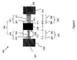
- FIG. 1is a schematic diagram of the FinFET 100 of the invention
- FIG. 2is a schematic diagram of the FinFET 200 of the invention.
- FIG. 3 ais a schematic diagram of the FinFET 300 of the invention.
- FIG. 3 bis a side view schematic diagram of the FinFET 300 ;
- FIG. 3 cis a schematic diagram of a series of FinFETs 300 ;
- FIG. 4 ais a schematic diagram of the FinFET 400 of the invention.
- FIG. 4 bis a side view schematic diagram of the FinFET 400 ;
- FIG. 4 cis a schematic diagram of a series of FinFETs 400 ;
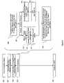
- FIG. 5is a schematic flow diagram illustrating a method of manufacturing the FinFET 100 ;
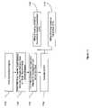
- FIG. 6is a schematic flow diagram illustrating a method of manufacturing the FinFET 200 ;
- FIG. 7is schematic diagrams of a partially completed FinFET 200 ;
- FIG. 8is schematic diagrams of a partially completed FinFET 200 ;
- FIG. 9is schematic diagrams of a partially completed FinFET 200 ;
- FIG. 10is schematic diagrams of a partially completed FinFET 200 ;
- FIG. 11is a schematic flow diagram illustrating a method of manufacturing the FinFET 300 ;
- FIG. 12is a schematic flow diagram illustrating a method of manufacturing the FinFET 400 .
- FIG. 13is schematic diagrams of a partially completed FinFET 400 .
- FinFETfin-type field effect transistor
- FinFET drive currentis optimized by configuring the FinFET asymmetrically to decrease fin resistance between the gate and the source region and to decrease capacitance between the gate and the drain region.
- device destruction at high voltagesis prevented by ballasting the FinFET.
- resistanceis optimized in the fin between the gate and both the source and drain regions (e.g., by increasing fin length, by blocking source/drain implant from the fin, and by blocking silicide formation on the top surface of the fin) so that the FinFET is operable at a predetermined maximum voltage.
- this ballastingcan prevent a chain reaction that can cause destruction of all FinFETs in the series.
- the FinFETs 100 , 200are designed with asymmetry between the source 101 , 201 and drain 102 , 202 regions.
- the gate and particularly, the gate conductor 120 , 220is placed closer to the point where the fin 150 , 250 merges into a single source strap (see item 101 of FIG. 1 ) or increases in width (see item 271 of FIG. 2 ) between the gate conductor and source strap.
- the gate conductor 120 , 220is place further from the point where the fin increases in width (see item 272 of FIG. 2 ) between the gate conductor and drain strap or from where the fin merges into a single drain strap (see item 102 of FIG. 1 ).
- one embodiment of the FinFET structure ( 100 , 200 ) of the inventioncomprises parallel semiconductor planes on a substrate that form a source region 101 , 201 and a drain region 102 , 202 .
- Another semiconductor planei.e., a 3-40 nm wide fin 150 , 250
- a gateis positioned on the fin 150 , 250 between the source 101 , 201 and drain regions 102 , 202 .
- a gate dielectric layeris formed on the opposing sidewalls of the fin between the source and drain regions.
- a gate conductor 120 , 220is form on the gate dielectric layer.
- the FinFET structure 100 , 200is asymmetrically configured such that a first resistance of the semiconductor fin 150 , 250 between the source region 101 , 201 and the gate conductor 120 , 220 is less than a second resistance of the semiconductor fin 150 , 250 between the gate conductor 120 , 220 and the drain region 102 , 202 and such that a first capacitance between the source region 101 , 201 and the gate conductor 120 , 220 is greater than a second capacitance between the gate conductor 120 , 220 and the drain region 102 , 202 .
- the gate conductor 120may be positioned on the fin 150 closer to the source region 101 than the drain region 102 . Positioning the gate conductor closer to the source region ensures that the first resistance between the gate conductor and the source region is less than the second resistance between the gate conductor and the drain region. Positioning the gate conductor farther away from the drain region decreases the capacitance between the gate and the drain region.
- the gate conductorcan be positioned equidistance 283 , 286 from the source 201 and drain 202 regions.
- the fin 250can be configured with a first portion 251 between the gate conductor 220 and the source region 201 and a second portion 252 between the gate conductor 220 and the drain region 202 .
- Both the first portion 251 and second portion 252can comprise inner sections 261 , 262 , respectively, adjacent the gate conductor 220 and outer sections 271 , 272 adjacent the inner sections 261 , 262 (i.e., between the inner section 261 and the source region 201 and between the inner section 262 and the drain region 202 ).
- the inner sections 261 , 262can have the same width (e.g., an approximately 3-40 nm first width 287 ).
- the outer sections 271 , 272can also have the same width (e.g., an approximately 9-200 nm second width 288 ) that is wider than the first width 287 of the inner sections 261 , 262 .
- Decreased capacitance between the gate conductor 220 and the drain region 202 as well as decreased resistance between the gate conductor 220 and the source region 201are provided if the inner section 262 of the second portion 252 is longer than the inner section 261 of the first portion 251 . Resistance is decreased between the gate conductor 220 and the source region 201 the closer the first wide section 271 is to the gate conductor 220 .
- optimal resistance and capacitancecan be achieved if the inner section 261 has a first length 284 that is approximately equal to the first width 287 and if the inner section 262 has a second length 282 that is greater than approximately three times the first width 287 .
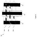
- another embodiment of the FinFET structure 300 , 400 of the inventioncomprises parallel semiconductor planes on a substrate that form a source region 301 , 401 and a drain region 302 , 402 .
- Another semiconductor planei.e., a 3-40 nm wide fin 350 , 450
- a gatee.g., comprising a gate dielectric layer and gate conductor 320 , 420
- the structures 300 , 400can also comprise spacers 311 - 312 , 411 - 412 formed over the fin 350 , 450 on the opposing sidewalls of the gate conductor 320 , 420 .
- the FinFET structure 300 , 400 of this embodimentis ballasted to prevent destruction at high voltages. As discussed above, at very high voltages FinFETs can enter a mode known as snap-back in which destruction of the FET can result due to current run-away in the hottest region of a transistor channel. This can occur with parallel sets of FinFET having a plurality of fins in which the hottest fin enters thermal run-away, conducting all additional current and ultimately causing the destruction of the FinFETs.
- the structures 300 , 400 of the inventionprovide a ballasted FinFET so that a maximum voltage/current that can be applied to a plurality of FinFETs in parallel (see items 390 , 490 of FIGS. 3 c and 4 c , respectively) can be increased to a predetermined maximum.
- equal lengths 383 of the semiconductor fin 350 between the gate conductor 320 and the source region 301 and the gate conductor 320 and the drain region 302 , respectively,are greater than approximately three to five times a width 388 (e.g., 9-200 nm) of the semiconductor fin 350 .
- This length 383can provide enough resistance within the semiconductor fin 350 so that the transistor 300 is operable at a predetermined maximum voltage. Additional resistance for ballasting can be provided if the semiconductor fin 350 is configured with a lesser concentration of dopants in the semiconductor fin than in the source/drain regions 301 , 302 .
- Additional resistancecan also be provided if the top surface 395 of the semiconductor fin is devoid of a silicide layer 391 .
- the source/drain regions 301 , 302can be implanted with an N+region 392 and topped with a silicide 391 ; however, during the manufacturing process silicide 391 and N+region 392 formation in the fin 350 can be blocked. Referring to FIG. 3 b , the source/drain regions 301 , 302 can be implanted with an N+region 392 and topped with a silicide 391 ; however, during the manufacturing process silicide 391 and N+region 392 formation in the fin 350 can be blocked. Referring to FIG.
- ballasting FinFETs 300 a - cprevents the fin with lowest breakdown voltage from entering thermal run-away and conducting all of the excess current, and ultimately causing the destruction of all FinFETs 300 a - c in the parallel set 390 .
- the semiconductor fin 450can comprise a first portion 451 between the source region 401 and the gate conductor 420 and second portion 452 between the gate conductor 420 and the drain region 402 .
- Both the first 451 and second 452 portionscomprise inner sections 461 , 462 , having the same width, e.g., 3-40 nm (i.e., first width 487 ), and the same length, e.g., 9-200 nm (i.e., first length 482 ).
- the inner sections 461 , 462are positioned immediately adjacent the gate conductor 420 .
- the first 451 and second 452 portionscan also each comprise outer sections 471 , 472 wide sections between the inner sections 461 , 462 and the source/drain regions 401 , 402 . Ballasting can be achieved if the length of the inner sections (i.e., the first length 482 ) is greater than approximately three to five times their width (i.e., first width 487 ). Specifically, the length 482 of the inner sections 461 , 462 narrow provides resistance within the fin 450 so that the transistor 400 is operable at a predetermined maximum voltage.
- Additional resistance for ballastingcan be provided if the inner sections 461 , 462 are configured a lesser concentration of source/drain dopants (i.e., p-type or n-type dopants) than the source/drain regions 401 , 402 and if the top surfaces 495 of the inner sections 461 , 462 are devoid of an adjacent silicide layer. For example, as illustrated in FIG.
- the source/drain regions 401 , 402 as well as the outer sections 471 , 472can be implanted with an N+region 492 and topped with a silicide 491 ; however, during the manufacturing process silicide 491 and N+region 492 formation in the inner sections 461 , 462 is blocked by spacers 411 , 412 . Referring to FIG.
- ballasting FinFETs 400 a - cprevents the fin with lowest breakdown voltage from entering thermal run-away and conducting all of the excess current, and ultimately causing the destruction of all FinFETs 400 a - c in the parallel set 490 .
- an embodiment of the method of manufacturing a fin-type field effect transistor, and particularly, an asymmetric FinFET 100incorporates conventional silicon-on-insulator (SOI) FinFET processing techniques.
- the methodcomprises forming the source/drain regions 101 , 102 ( 500 ) and forming the approximately 3-40 nm semiconductor fin 150 that extends from the source region 101 to the drain region 102 ( 502 ).
- the source/drain regions and the fincan be lithographically patterned and etched into a silicon layer of an SOI wafer such that the source/drain regions are formed as parallel planes and the fin(s) extend between the source region and the drain region.
- a hard maskmay be deposited above the silicon layer.
- Asymmetryis provided by forming a gate (e.g., gate dielectric layer and gate conductor 120 ) adjacent to the semiconductor fin 150 such that the gate conductor 120 is closer to the source region 101 than the drain region 102 ( 504 ).
- a gatee.g., gate dielectric layer and gate conductor 120
- a sacrificial oxidecan be grown on the fin and, particularly, on the exposed silicon surfaces of the fin and the source/drain regions and then stripped to remove any irregularities.
- a gate dielectric layercan be grown or deposited on the sidewalls and top surface of the fin.
- a conductive materialsuch as a polysilicon, can be deposited over the fin, lithographically patterned and etched. In this embodiment, the gate conductor that is formed is positioned closer to the source region.
- the asymmetry in the placement of gate conductor 120 between the source and drain regionsresults a first resistance of the semiconductor fin 150 between the source region 101 and the gate conductor 120 that is less than a second resistance of the semiconductor fin 150 between the gate conductor 120 and the drain region 102 .
- This asymmetryalso results in a first capacitance between the source region 101 and the gate conductor 120 that is greater than a second capacitance between the gate conductor 120 and the drain region 102 .
- forming the gate conductor 120 adjacent to the semiconductor fin 150such that the gate conductor 120 is closer to the source region 101 than the drain region 102 decreases the resistance in the fin 15 O between the source region 101 and the gate conductor 120 and decreases the capacitance between the gate conductor 120 and the drain region 102 .
- Additional processingcan be performed to complete the FinFET 100 ( 506 ).
- This additional processingmay include, but is not limited to: stripping the optional hard mask by a directional reactive ion etching process; implanting source/drain extensions (i.e., implanting sections of fin between gate conductor and the source/drain regions); forming halos; forming fin spacers; forming spacers on gate sidewalls; implanting N+ into the source/drain regions; forming a silicide layer (e.g., Co, Ni, Etc.) on the top surface of the fin, on the top surface of the source/drain regions, and/or on the top surface of the gate conductor if the gate conductor is formed with a polysilicon material and without a cap; depositing and planarizing an additional dielectric layer, forming gate contacts, forming source/drain contacts, etc. It should be noted that the same processing steps can be used to simultaneously form multiple transistors 100 in which multiple semiconductor fins share the same source/drain straps.
- an alternative embodiment of the method of manufacturing an asymmetric FinFET 200also incorporates conventional silicon-on-insulator (SOI) FinFET processing techniques.
- the methodcomprises forming the source/drain regions 201 , 202 ( 600 ) and forming a narrow semiconductor fin 250 that extends from the source region 201 to the drain region 202 ( 602 ), as described in detail above.
- the gateincluding the gate conductor 220
- the gatecan be formed adjacent the semiconductor fin 250 equidistance 283 between the source region 201 and the drain region 202 ( 604 ).
- the dimensions of the fin on either side of the gate conductorare adjusted to vary the first resistance within a first portion of the fin between the gate conductor and the source region and a second resistance of a second portion of the fin between the gate conductor and the drain region ( 605 ).
- the dimensions of the first portion 251can be adjusted so that a first inner section 261 , having a first width 287 (e.g., 3-40 nm), is positioned adjacent to the gate conductor 220 and a first outer section 271 , having a second width 288 that is greater than the first width 287 , is positioned between the first inner section 261 and the source region 201 .
- the dimensions of the second portion 252can be adjusted to form a second inner section 262 and a second outer section 272 .
- the inner sectionscan each have the same width 287 and the outer sections can have the same width 288 .
- Asymmetrycan be achieved if the second inner section 262 is longer than the first inner section 262 , thereby, decreasing the resistance in the fin 250 between the source region 201 and the gate conductor 220 and decreasing the capacitance between the gate conductor 220 and the drain region 201 .
- Optimal asymmetrycan be achieved if the first inner section 261 is formed with a first length 284 that is approximately equal to the first width 287 (e.g., 3-40 nm) and the second inner section 262 is formed with a second length 282 that is greater than approximately three to five times the first width 287 (e.g., 9-200 nm).
- first 211 and second 212 spacersare simultaneously formed immediately on the sides 221 , 222 of the gate conductor 220 over the first portion 251 and second portion 252 , respectively, of the fin 250 ( 606 , see FIG. 7 )).
- the spacers 211 , 212may be formed by growing or depositing an approximately 9-200 nm thick silicon dioxide layer on the sides 221 , 222 of the gate conductor 220 .
- the spacers 211 , 212can initially be formed to have the same thickness 282 .
- This thickness 282should be greater than approximately three to five times the width 287 (i.e., first width) of the fin as originally formed (e.g., 3-40 nm).
- the spacers 211 , 212may each be approximately 9-200 nm thick. Additionally, the spacers 211 , 212 should be formed such that a first exposed section 276 of the first portion 251 of the fin 250 remains between the first spacer 211 and the source region 201 and a second exposed section 275 of the second portion 252 of the fin 250 remains between the second spacer 212 and the drain region 202 .
- the size (i.e., thickness 282 ) of the first spacer 211is reduced such that the spacer 211 has another thickness 284 that is approximately equal to the first width 287 ( 608 , see FIG. 2 ).
- One technique for reducing the thickness of the first spacercomprises masking 277 the second spacer 212 ( 610 , see FIG. 8 ) and then isotropically etching the first spacer ( 612 , see FIG. 8 ). The etching process etches back not only the top surface 213 of the first spacer 211 but also the exposed sidewall 215 of the first spacer 211 , thus, reducing the spacer thickness.
- the mask 277is removed ( 614 ).
- Another technique for reducing the thickness of the first spacercomprises implanting an inert species 217 (e.g., silicon, argon, xenon, etc) into the silicon dioxide spacers 211 , 212 from an angle 216 ( ⁇ 90 degrees) towards the first spacer 211 such that implantation of the second spacer 212 is shadowed (i.e., partially blocked) by the gate conductor 220 .
- the first spacer 211receives a greater concentration of the inert material 217 which enhances the etch rate of the first spacer 211 ( 616 , see FIG. 9 ).
- first spacer 211 with the greater concentration of the inert species 217is etched at a faster rate than the second spacer 212 ( 618 , see FIG. 10 ).
- the etching process ( 618 )etches back not only the top surface 213 of the first spacer 211 but also the exposed sidewall 215 of the first spacer 211 , thus, reducing the spacer thickness.
- additional semiconductor materiale.g., silicon, silicon germanium, silicon germanium carbide, etc.
- additional semiconductor materiale.g., silicon, silicon germanium, silicon germanium carbide, etc.
- the process ( 620 ) of forming the additional semiconductor materialcan be accomplished by selectively growing silicon, silicon germanium, or silicon germanium carbide, on the exposed sections 275 , 276 of the fin 250 as well as on the silicon source/drain regions. This process ( 620 ) forms the first and second outer sections 271 , 272 (see FIG. 2 ).
- first and second inner sections 261 , 262are those sections of the fin 250 that remain under the first 211 and second 212 spacers, respectively. Additional processing may be performed to complete the FinFET 200 ( 622 of FIG. 6 ), as described in detail above. It should be noted that the same processing steps can be used to simultaneously form multiple transistors 200 in which multiple semiconductor fins share the same source/drain straps.
- an embodiment of the method of manufacturing a fin-type field effect transistor, and particularly, a ballasted FinFET 300comprises forming the source/drain regions 301 , 302 as well as forming the semiconductor fin 350 using conventional FinFET processing technology ( 1100 - 1102 ), as described in detail above.
- a gateincluding a gate dielectric layer and a gate conductor 320 , is formed adjacent to the semiconductor fin such that the gate conductor 320 is equidistance 383 between the source region 301 and the drain region 302 ( 1104 , see detail description of gate formation process above).
- Ballastingcan be achieved by forming the gate such that the length 383 of the fin 350 between either the gate conductor 320 and the source region 301 or the gate conductor 320 and the drain region 302 is greater than approximately three times a width 388 of the semiconductor fin 350 .
- This length 383provides added resistance within the semiconductor fin 350 so that the transistor 300 is operable at a predetermined maximum voltage.
- Additional resistance for ballastingcan be provided by forming the semiconductor fin 350 with a lesser concentration of source/drain dopants than the source/drain regions ( 1108 ) (e.g., by blocking implantation of an N+region 392 into the fin 350 at process 1106 , see FIG. 3 b ) and without a silicide layer on the top surface 395 of the fin 350 ( 1110 ) (e.g., by blocking formation of the silicide layer 391 on the top surface 395 of the fin 350 at process 1106 , see FIG. 3 b ). It should be noted that the same processing steps can be used to simultaneously form multiple transistors 300 in which multiple semiconductor fins share the same source/drain straps (see FIG. 3 c ).
- an embodiment of the method of manufacturing the ballasted FinFET 400comprises forming the source/drain regions 401 , 402 as well as forming a narrow semiconductor fin 450 using conventional FinFET processing technology ( 1200 - 1202 , see detailed description above).
- a gateincluding a gate dielectric layer and a gate conductor 420 , is formed adjacent to the semiconductor fin 450 such that the gate conductor 420 is equidistance 483 between the source region 401 and the drain region 402 ( 1204 , see detailed description above).
- the dimensions of the fincan be adjusted to optimize resistance so that the transistor is operable at a predetermined maximum voltage ( 1205 ).
- the dimensions of the finsmay be adjusted by forming outer sections of the fin adjacent to the source/drain that are wider than inner sections of the fin adjacent to the gate conductor. Specifically, the dimensions of both a first portion 451 of the fin 450 not covered by the gate conductor 420 that extends between the source region 401 and the gate conductor 420 and a second portion 452 that extends between the gate conductor 420 and the drain region 402 can adjusted. The dimensions can be adjusted so that inner sections 461 , 462 that have the same width 487 (i.e., a first width 487 ) and the same length (i.e., first length 482 ) are positioned adjacent the gate conductor.
- outer sections 471 , 472have the same width 488 (i.e., second width) and the same length 481 (i.e., second length) and are positioned adjacent the source/drain regions.
- the outer sections 471 , 472are formed such that their width 488 is greater than the width 487 of the inner sections 461 , 462 .
- Ballastingis achieved by forming the inner and outer sections so that the length 482 of the inner sections 461 , 462 is greater than approximately three times the original width of the fin (i.e., first width 487 ), thereby, providing enough resistance within the first and second inner sections 461 , 462 so that the transistor 400 is operable at a predetermined maximum voltage.
- spacers 411 , 412are formed over the first and second portions 451 , 452 of the fin 450 (e.g., on the top surface and opposing sidewalls of the fin 450 ) immediately adjacent the sides 421 , 422 of the gate conductor 420 ( 1206 , see FIG. 13 ).
- the spacers 411 , 412can be formed (e.g., by growing or depositing a silicon dioxide) with a thickness 482 that is greater than approximately three to five times the first width 487 (i.e., the width of the fin (e.g., 3-40 nm) as initially formed at process ( 1202 )).
- the spacersshould also be formed such that first and second exposed sections 476 , 475 of the fin 450 remain between the spacers 411 , 412 and the source/drain regions 401 , 402 .
- first and second inner sections 461 , 462are those sections of the fin 450 that remain under the spacers 411 , 412 .
- the length of the inner sectionsis a function of the thickness of the spacers.
- Additional processing stepsmay be performed to complete FinFET ( 1210 ), as described in detail above. Additional resistance for ballasting can be provided by forming the first and second inner sections 461 , 462 of the semiconductor fin 450 with a source/drain dopant concentration that is less than that of the source/drain regions ( 1212 ) (e.g., by blocking implantation of an N+region 492 into the fin 450 at process 1210 , see FIG.
- FinFETfin-type field effect transistor
- FinFET drive currentis optimized by configuring the FinFET asymmetrically to decrease fin resistance between the gate and the source region and to decrease capacitance between the gate and the drain region. Due to this simultaneously low source-gate resistance and low drain-gate capacitance, such asymmetric FinFETS can provide circuits having higher switching speed and reduced power. This also translates into physically smaller circuits, and hence lower cost circuits, since fewer fins can provide equivalent speed.
- device destruction at high voltagesis prevented by ballasting the FinFET.
- resistanceis optimized in the fin between the gate and both the source and drain regions (e.g., by increasing fin length, by blocking source/drain implant from the fin, and by blocking silicide formation on the top surface of the fin) so that the FinFET is operable at a predetermined maximum voltage.
- Such ballasted FinFETsprovide for higher reliability at higher operation voltage, and can avoid special, costly processing steps otherwise required to add special high-voltage transistors to a circuit.
Landscapes
- Thin Film Transistor (AREA)
- Insulated Gate Type Field-Effect Transistor (AREA)
- Bipolar Transistors (AREA)
Abstract
Description
Claims (13)
Priority Applications (11)
| Application Number | Priority Date | Filing Date | Title |
|---|---|---|---|
| US11/161,442US7348642B2 (en) | 2005-08-03 | 2005-08-03 | Fin-type field effect transistor |
| AT06788172TATE544182T1 (en) | 2005-08-03 | 2006-07-21 | FIN TYPE FIELD EFFECT TRANSISTOR |
| PCT/US2006/028465WO2007019023A2 (en) | 2005-08-03 | 2006-07-21 | Fin-type field effect transistor |
| CN2006800285758ACN101443912B (en) | 2005-08-03 | 2006-07-21 | Fin-type field effect transistor |
| JP2008525007AJP5220604B2 (en) | 2005-08-03 | 2006-07-21 | Fin-type field effect transistor and manufacturing method thereof |
| EP06788172AEP1920467B1 (en) | 2005-08-03 | 2006-07-21 | Fin-type field effect transistor |
| KR1020087004466AKR101027173B1 (en) | 2005-08-03 | 2006-07-21 | Fin Field Effect Transistor |
| TW095128273ATWI397999B (en) | 2005-08-03 | 2006-08-02 | Fin field effect transistor |
| US11/955,579US8129773B2 (en) | 2005-08-03 | 2007-12-13 | Fin-type field effect transistor |
| US11/972,412US8106439B2 (en) | 2005-08-03 | 2008-01-10 | Fin-type field effect transistor |
| US13/361,050US8524547B2 (en) | 2005-08-03 | 2012-01-30 | Fin-type field effect transistor |
Applications Claiming Priority (1)
| Application Number | Priority Date | Filing Date | Title |
|---|---|---|---|
| US11/161,442US7348642B2 (en) | 2005-08-03 | 2005-08-03 | Fin-type field effect transistor |
Related Child Applications (2)
| Application Number | Title | Priority Date | Filing Date |
|---|---|---|---|
| US11/955,579ContinuationUS8129773B2 (en) | 2005-08-03 | 2007-12-13 | Fin-type field effect transistor |
| US11/972,412DivisionUS8106439B2 (en) | 2005-08-03 | 2008-01-10 | Fin-type field effect transistor |
Publications (2)
| Publication Number | Publication Date |
|---|---|
| US20070029624A1 US20070029624A1 (en) | 2007-02-08 |
| US7348642B2true US7348642B2 (en) | 2008-03-25 |
Family
ID=37716900
Family Applications (4)
| Application Number | Title | Priority Date | Filing Date |
|---|---|---|---|
| US11/161,442Expired - LifetimeUS7348642B2 (en) | 2005-08-03 | 2005-08-03 | Fin-type field effect transistor |
| US11/955,579Active2026-03-05US8129773B2 (en) | 2005-08-03 | 2007-12-13 | Fin-type field effect transistor |
| US11/972,412Active2028-01-30US8106439B2 (en) | 2005-08-03 | 2008-01-10 | Fin-type field effect transistor |
| US13/361,050Expired - LifetimeUS8524547B2 (en) | 2005-08-03 | 2012-01-30 | Fin-type field effect transistor |
Family Applications After (3)
| Application Number | Title | Priority Date | Filing Date |
|---|---|---|---|
| US11/955,579Active2026-03-05US8129773B2 (en) | 2005-08-03 | 2007-12-13 | Fin-type field effect transistor |
| US11/972,412Active2028-01-30US8106439B2 (en) | 2005-08-03 | 2008-01-10 | Fin-type field effect transistor |
| US13/361,050Expired - LifetimeUS8524547B2 (en) | 2005-08-03 | 2012-01-30 | Fin-type field effect transistor |
Country Status (8)
| Country | Link |
|---|---|
| US (4) | US7348642B2 (en) |
| EP (1) | EP1920467B1 (en) |
| JP (1) | JP5220604B2 (en) |
| KR (1) | KR101027173B1 (en) |
| CN (1) | CN101443912B (en) |
| AT (1) | ATE544182T1 (en) |
| TW (1) | TWI397999B (en) |
| WO (1) | WO2007019023A2 (en) |
Cited By (30)
| Publication number | Priority date | Publication date | Assignee | Title |
|---|---|---|---|---|
| US20070034969A1 (en)* | 2005-08-12 | 2007-02-15 | Texas Instruments Inc. | Semiconductor device having a gate electrode material feature located adjacent a gate width side of its gate electrode and a method of manufacture therefor |
| US20070040221A1 (en)* | 2005-08-19 | 2007-02-22 | Harald Gossner | Electrostatic discharge protection element |
| US20100038694A1 (en)* | 2008-08-15 | 2010-02-18 | Anderson Brent A | Split-gate dram with mugfet, design structure, and method of manufacture |
| US20100041191A1 (en)* | 2008-08-15 | 2010-02-18 | Anderson Brent A | Split-gate dram with mugfet, design structure, and method of manufacture |
| US20100296213A1 (en)* | 2009-02-19 | 2010-11-25 | Jam-Wem Lee | ESD Protection for FinFETs |
| US20110027948A1 (en)* | 2009-07-31 | 2011-02-03 | International Business Machines Corporation | Method for manufacturing a finfet device |
| US7898041B2 (en)* | 2005-06-30 | 2011-03-01 | Intel Corporation | Block contact architectures for nanoscale channel transistors |
| US7989280B2 (en) | 2005-11-30 | 2011-08-02 | Intel Corporation | Dielectric interface for group III-V semiconductor device |
| US8071983B2 (en) | 2005-06-21 | 2011-12-06 | Intel Corporation | Semiconductor device structures and methods of forming semiconductor structures |
| US8084818B2 (en) | 2004-06-30 | 2011-12-27 | Intel Corporation | High mobility tri-gate devices and methods of fabrication |
| US8183646B2 (en) | 2005-02-23 | 2012-05-22 | Intel Corporation | Field effect transistor with narrow bandgap source and drain regions and method of fabrication |
| US8184472B2 (en) | 2009-03-13 | 2012-05-22 | International Business Machines Corporation | Split-gate DRAM with lateral control-gate MuGFET |
| US8273626B2 (en) | 2003-06-27 | 2012-09-25 | Intel Corporationn | Nonplanar semiconductor device with partially or fully wrapped around gate electrode and methods of fabrication |
| US8294180B2 (en) | 2005-09-28 | 2012-10-23 | Intel Corporation | CMOS devices with a single work function gate electrode and method of fabrication |
| US8362566B2 (en) | 2008-06-23 | 2013-01-29 | Intel Corporation | Stress in trigate devices using complimentary gate fill materials |
| US8502351B2 (en) | 2004-10-25 | 2013-08-06 | Intel Corporation | Nonplanar device with thinned lower body portion and method of fabrication |
| US8513102B2 (en) | 2010-11-08 | 2013-08-20 | Leonard Forbes | Reduction of random telegraph signal (RTS) and 1/f noise in silicon MOS devices, circuits, and sensors |
| US8617945B2 (en) | 2006-08-02 | 2013-12-31 | Intel Corporation | Stacking fault and twin blocking barrier for integrating III-V on Si |
| US8686516B2 (en)* | 2011-09-08 | 2014-04-01 | Taiwan Semiconductor Manufacturing Company, Ltd. | Silicide formation and associated devices |
| US9190466B2 (en) | 2013-12-27 | 2015-11-17 | International Business Machines Corporation | Independent gate vertical FinFET structure |
| US20160056154A1 (en)* | 2014-08-22 | 2016-02-25 | Renesas Electronics Corporation | Semiconductor device |
| US9281065B2 (en) | 2014-08-11 | 2016-03-08 | Empire Technology Development Llc | Low-power nonvolatile memory cells with select gates |
| US9299711B2 (en) | 2012-09-26 | 2016-03-29 | Samsung Electronics Co., Ltd. | Field effect transistors including asymmetrical silicide structures and related devices |
| US9337307B2 (en) | 2005-06-15 | 2016-05-10 | Intel Corporation | Method for fabricating transistor with thinned channel |
| US9484306B1 (en) | 2015-11-17 | 2016-11-01 | International Business Machines Corporation | MOSFET with asymmetric self-aligned contact |
| US20170074728A1 (en)* | 2015-09-16 | 2017-03-16 | Qualcomm Incorporated | Transistor temperature sensing |
| US9634092B2 (en) | 2015-02-26 | 2017-04-25 | Samsung Electronics Co., Ltd. | Semiconductor devices having tapered active regions |
| US9691763B2 (en) | 2013-12-27 | 2017-06-27 | International Business Machines Corporation | Multi-gate FinFET semiconductor device with flexible design width |
| US10559690B2 (en) | 2014-09-18 | 2020-02-11 | International Business Machines Corporation | Embedded source/drain structure for tall FinFET and method of formation |
| US11233051B2 (en) | 2019-10-02 | 2022-01-25 | Samsung Electronics Co., Ltd. | Integrated circuit device and method of manufacturing the same |
Families Citing this family (37)
| Publication number | Priority date | Publication date | Assignee | Title |
|---|---|---|---|---|
| US7268058B2 (en)* | 2004-01-16 | 2007-09-11 | Intel Corporation | Tri-gate transistors and methods to fabricate same |
| US7332439B2 (en)* | 2004-09-29 | 2008-02-19 | Intel Corporation | Metal gate transistors with epitaxial source and drain regions |
| US7348642B2 (en)* | 2005-08-03 | 2008-03-25 | International Business Machines Corporation | Fin-type field effect transistor |
| JP2008177278A (en)* | 2007-01-17 | 2008-07-31 | Toshiba Corp | Static semiconductor memory device |
| KR100887007B1 (en) | 2007-10-12 | 2009-03-04 | 주식회사 동부하이텍 | Method and structure of poly pattern formation in LD-string of Al-string |
| US7994612B2 (en)* | 2008-04-21 | 2011-08-09 | International Business Machines Corporation | FinFETs single-sided implant formation |
| WO2009130629A1 (en)* | 2008-04-23 | 2009-10-29 | Nxp B.V. | A fin fet and a method of manufacturing a fin fet |
| US8946028B2 (en)* | 2009-10-06 | 2015-02-03 | International Business Machines Corporation | Merged FinFETs and method of manufacturing the same |
| US8716797B2 (en)* | 2009-11-03 | 2014-05-06 | International Business Machines Corporation | FinFET spacer formation by oriented implantation |
| US8174055B2 (en)* | 2010-02-17 | 2012-05-08 | Globalfoundries Inc. | Formation of FinFET gate spacer |
| JP2012243971A (en)* | 2011-05-20 | 2012-12-10 | Sony Corp | Bootstrap circuit, inverter circuit, scanning circuit, display device, and electronic apparatus |
| CN102760735B (en)* | 2011-06-21 | 2015-06-17 | 钰创科技股份有限公司 | Dynamic memory structure |
| US8595661B2 (en) | 2011-07-29 | 2013-11-26 | Synopsys, Inc. | N-channel and p-channel finFET cell architecture |
| KR101805634B1 (en)* | 2011-11-15 | 2017-12-08 | 삼성전자 주식회사 | Semiconductor device comprising III-V group barrier and method of manufacturing the same |
| CN103165428B (en)* | 2011-12-14 | 2015-12-09 | 中芯国际集成电路制造(上海)有限公司 | Make the method for semiconductor device |
| US8901659B2 (en)* | 2012-02-09 | 2014-12-02 | International Business Machines Corporation | Tapered nanowire structure with reduced off current |
| US8637371B2 (en) | 2012-02-16 | 2014-01-28 | International Business Machines Corporation | Non-planar MOSFET structures with asymmetric recessed source drains and methods for making the same |
| US8927432B2 (en)* | 2012-06-14 | 2015-01-06 | International Business Machines Corporation | Continuously scalable width and height semiconductor fins |
| CN103779217A (en)* | 2012-10-18 | 2014-05-07 | 中芯国际集成电路制造(上海)有限公司 | Fin type field effect transistor and fabrication method thereof |
| CN103811338B (en)* | 2012-11-08 | 2016-12-21 | 中芯国际集成电路制造(上海)有限公司 | A kind of semiconductor device and preparation method thereof |
| US9123654B2 (en)* | 2013-02-15 | 2015-09-01 | International Business Machines Corporation | Trilayer SIT process with transfer layer for FINFET patterning |
| US9231106B2 (en)* | 2013-03-08 | 2016-01-05 | Taiwan Semiconductor Manufacturing Company, Ltd. | FinFET with an asymmetric source/drain structure and method of making same |
| CN104103319B (en)* | 2013-04-11 | 2017-08-25 | 中芯国际集成电路制造(上海)有限公司 | Anti-fuse circuit and its programmed method, anti-fuse structures |
| KR102089682B1 (en) | 2013-07-15 | 2020-03-16 | 삼성전자 주식회사 | Semiconductor device and method for fabricating the same |
| US9484460B2 (en) | 2013-09-19 | 2016-11-01 | Taiwan Semiconductor Manufacturing Company Limited | Semiconductor device having gate dielectric surrounding at least some of channel region and gate electrode surrounding at least some of gate dielectric |
| US9633906B2 (en) | 2014-01-24 | 2017-04-25 | International Business Machines Corporation | Gate structure cut after formation of epitaxial active regions |
| WO2015147783A1 (en) | 2014-03-24 | 2015-10-01 | Intel Corporation | Techniques for achieving multiple transistor fin dimensions on a single die |
| US9318574B2 (en)* | 2014-06-18 | 2016-04-19 | International Business Machines Corporation | Method and structure for enabling high aspect ratio sacrificial gates |
| KR102168302B1 (en) | 2014-11-21 | 2020-10-22 | 삼성전자주식회사 | Semiconductor device using three dimensional channel |
| TWI594421B (en)* | 2016-06-28 | 2017-08-01 | 瑞昱半導體股份有限公司 | Fin field effect transistor and manufacturing method thereof |
| CN107579116A (en)* | 2016-07-05 | 2018-01-12 | 瑞昱半导体股份有限公司 | Fin field effect transistor and manufacturing method thereof |
| KR101859587B1 (en) | 2016-12-30 | 2018-05-18 | 서울시립대학교 산학협력단 | Nagative capacitance finfet device and manufacturing method therefor |
| US10475790B2 (en)* | 2017-09-28 | 2019-11-12 | Taiwan Semiconductor Manufacturing Co., Ltd. | Asymmetric gate pitch |
| KR102446403B1 (en)* | 2018-06-22 | 2022-09-21 | 삼성전자주식회사 | Semiconductor device, method for fabricating the same and layout design method for the same |
| JP6612937B2 (en)* | 2018-07-18 | 2019-11-27 | ルネサスエレクトロニクス株式会社 | Semiconductor device |
| US11060846B2 (en) | 2018-12-19 | 2021-07-13 | Kla Corporation | Scatterometry based methods and systems for measurement of strain in semiconductor structures |
| US11670675B2 (en) | 2020-12-04 | 2023-06-06 | United Semiconductor Japan Co., Ltd. | Semiconductor device |
Citations (20)
| Publication number | Priority date | Publication date | Assignee | Title |
|---|---|---|---|---|
| JPS6226865A (en) | 1985-07-29 | 1987-02-04 | New Japan Radio Co Ltd | Field effect transistor |
| JPS62132366A (en) | 1985-12-04 | 1987-06-15 | Nec Corp | Manufacturing method of vertical field effect transistor |
| US4907041A (en)* | 1988-09-16 | 1990-03-06 | Xerox Corporation | Intra-gate offset high voltage thin film transistor with misalignment immunity |
| US5399896A (en) | 1992-09-29 | 1995-03-21 | Mitsubishi Denki Kabushiki Kaisha | FET with a T-shaped gate of a particular structure |
| US5985724A (en) | 1996-10-01 | 1999-11-16 | Advanced Micro Devices, Inc. | Method for forming asymmetrical p-channel transistor having nitrided oxide patterned to selectively form a sidewall spacer |
| US20020036328A1 (en) | 1998-11-16 | 2002-03-28 | William R. Richards, Jr. | Offset drain fermi-threshold field effect transistors |
| US6413802B1 (en) | 2000-10-23 | 2002-07-02 | The Regents Of The University Of California | Finfet transistor structures having a double gate channel extending vertically from a substrate and methods of manufacture |
| US20020171113A1 (en) | 2001-05-15 | 2002-11-21 | Mitsubishi Denki Kabushiki Kaisha | Semiconductor device and method of manufacturing the device |
| US6534787B2 (en) | 1998-11-18 | 2003-03-18 | Sharp Laboratories Of America, Inc. | Asymmetrical MOS channel structure with drain extension |
| US20040031979A1 (en) | 2002-06-07 | 2004-02-19 | Amberwave Systems Corporation | Strained-semiconductor-on-insulator device structures |
| US6706571B1 (en) | 2002-10-22 | 2004-03-16 | Advanced Micro Devices, Inc. | Method for forming multiple structures in a semiconductor device |
| US6740914B2 (en) | 2001-04-27 | 2004-05-25 | Fujistu Limited | FET circuit block with reduced self-heating |
| US20040099885A1 (en) | 2002-11-26 | 2004-05-27 | Taiwan Semiconductor Manufacturing Co., Ltd. | CMOS SRAM cell configured using multiple-gate transistors |
| US20040145000A1 (en) | 2003-01-23 | 2004-07-29 | An Judy Xilin | Tri-gate and gate around MOSFET devices and methods for making same |
| US6800885B1 (en) | 2003-03-12 | 2004-10-05 | Advance Micro Devices, Inc. | Asymmetrical double gate or all-around gate MOSFET devices and methods for making same |
| US20050205944A1 (en)* | 2004-03-18 | 2005-09-22 | International Business Machines Corporation | Multiple dielectric finfet structure and method |
| US20050224800A1 (en)* | 2004-03-31 | 2005-10-13 | Nick Lindert | Bulk non-planar transistor having strained enhanced mobility and methods of fabrication |
| US20050285189A1 (en)* | 2004-06-28 | 2005-12-29 | Shibib Muhammed A | Graded conductive structure for use in a metal-oxide-semiconductor device |
| US6992358B2 (en)* | 2003-12-05 | 2006-01-31 | Kabushiki Kaisha Toshiba | Semiconductor device and method for manufacturing the same |
| US20060273409A1 (en)* | 2005-05-23 | 2006-12-07 | Wen-Chin Lee | High performance CMOS with metal-gate and Schottky source/drain |
Family Cites Families (19)
| Publication number | Priority date | Publication date | Assignee | Title |
|---|---|---|---|---|
| US539896A (en)* | 1895-05-28 | John graves | ||
| JPS6226665A (en) | 1985-07-26 | 1987-02-04 | Hitachi Ltd | magnetic disk drive |
| JPS63308962A (en)* | 1987-06-11 | 1988-12-16 | Sanyo Electric Co Ltd | Manufacture of semiconductor device |
| JP3543946B2 (en)* | 2000-04-14 | 2004-07-21 | 日本電気株式会社 | Field effect transistor and method of manufacturing the same |
| EP1292989A1 (en)* | 2000-05-10 | 2003-03-19 | Koninklijke Philips Electronics N.V. | A semiconductor device |
| JP3729082B2 (en)* | 2001-04-25 | 2005-12-21 | 日本電信電話株式会社 | Semiconductor protection circuit |
| US6492212B1 (en)* | 2001-10-05 | 2002-12-10 | International Business Machines Corporation | Variable threshold voltage double gated transistors and method of fabrication |
| US6967351B2 (en)* | 2001-12-04 | 2005-11-22 | International Business Machines Corporation | Finfet SRAM cell using low mobility plane for cell stability and method for forming |
| JP3605086B2 (en) | 2002-03-29 | 2004-12-22 | 株式会社東芝 | Field effect transistor |
| US6664582B2 (en)* | 2002-04-12 | 2003-12-16 | International Business Machines Corporation | Fin memory cell and method of fabrication |
| US6764884B1 (en)* | 2003-04-03 | 2004-07-20 | Advanced Micro Devices, Inc. | Method for forming a gate in a FinFET device and thinning a fin in a channel region of the FinFET device |
| US7456476B2 (en)* | 2003-06-27 | 2008-11-25 | Intel Corporation | Nonplanar semiconductor device with partially or fully wrapped around gate electrode and methods of fabrication |
| US6897111B2 (en)* | 2003-07-28 | 2005-05-24 | Chartered Semiconductor Manufacturing Ltd. | Method using quasi-planar double gated fin field effect transistor process for the fabrication of a thyristor-based static read/write random-access memory |
| JP2005086024A (en)* | 2003-09-09 | 2005-03-31 | Toshiba Corp | Semiconductor device and method for manufacturing same |
| JP2005142289A (en)* | 2003-11-05 | 2005-06-02 | Toshiba Corp | Semiconductor memory device |
| US7176092B2 (en)* | 2004-04-16 | 2007-02-13 | Taiwan Semiconductor Manufacturing Company | Gate electrode for a semiconductor fin device |
| US20060071270A1 (en)* | 2004-09-29 | 2006-04-06 | Shibib Muhammed A | Metal-oxide-semiconductor device having trenched diffusion region and method of forming same |
| DE602005006093T2 (en)* | 2005-02-21 | 2009-05-20 | Interuniversitair Microelektronica Centrum (Imec) | Semiconductor memory device with floating body and manufacturing method thereof |
| US7348642B2 (en)* | 2005-08-03 | 2008-03-25 | International Business Machines Corporation | Fin-type field effect transistor |
- 2005
- 2005-08-03USUS11/161,442patent/US7348642B2/ennot_activeExpired - Lifetime
- 2006
- 2006-07-21JPJP2008525007Apatent/JP5220604B2/ennot_activeExpired - Fee Related
- 2006-07-21CNCN2006800285758Apatent/CN101443912B/enactiveActive
- 2006-07-21EPEP06788172Apatent/EP1920467B1/enactiveActive
- 2006-07-21ATAT06788172Tpatent/ATE544182T1/enactive
- 2006-07-21WOPCT/US2006/028465patent/WO2007019023A2/enactiveApplication Filing
- 2006-07-21KRKR1020087004466Apatent/KR101027173B1/ennot_activeExpired - Fee Related
- 2006-08-02TWTW095128273Apatent/TWI397999B/enactive
- 2007
- 2007-12-13USUS11/955,579patent/US8129773B2/enactiveActive
- 2008
- 2008-01-10USUS11/972,412patent/US8106439B2/enactiveActive
- 2012
- 2012-01-30USUS13/361,050patent/US8524547B2/ennot_activeExpired - Lifetime
Patent Citations (20)
| Publication number | Priority date | Publication date | Assignee | Title |
|---|---|---|---|---|
| JPS6226865A (en) | 1985-07-29 | 1987-02-04 | New Japan Radio Co Ltd | Field effect transistor |
| JPS62132366A (en) | 1985-12-04 | 1987-06-15 | Nec Corp | Manufacturing method of vertical field effect transistor |
| US4907041A (en)* | 1988-09-16 | 1990-03-06 | Xerox Corporation | Intra-gate offset high voltage thin film transistor with misalignment immunity |
| US5399896A (en) | 1992-09-29 | 1995-03-21 | Mitsubishi Denki Kabushiki Kaisha | FET with a T-shaped gate of a particular structure |
| US5985724A (en) | 1996-10-01 | 1999-11-16 | Advanced Micro Devices, Inc. | Method for forming asymmetrical p-channel transistor having nitrided oxide patterned to selectively form a sidewall spacer |
| US20020036328A1 (en) | 1998-11-16 | 2002-03-28 | William R. Richards, Jr. | Offset drain fermi-threshold field effect transistors |
| US6534787B2 (en) | 1998-11-18 | 2003-03-18 | Sharp Laboratories Of America, Inc. | Asymmetrical MOS channel structure with drain extension |
| US6413802B1 (en) | 2000-10-23 | 2002-07-02 | The Regents Of The University Of California | Finfet transistor structures having a double gate channel extending vertically from a substrate and methods of manufacture |
| US6740914B2 (en) | 2001-04-27 | 2004-05-25 | Fujistu Limited | FET circuit block with reduced self-heating |
| US20020171113A1 (en) | 2001-05-15 | 2002-11-21 | Mitsubishi Denki Kabushiki Kaisha | Semiconductor device and method of manufacturing the device |
| US20040031979A1 (en) | 2002-06-07 | 2004-02-19 | Amberwave Systems Corporation | Strained-semiconductor-on-insulator device structures |
| US6706571B1 (en) | 2002-10-22 | 2004-03-16 | Advanced Micro Devices, Inc. | Method for forming multiple structures in a semiconductor device |
| US20040099885A1 (en) | 2002-11-26 | 2004-05-27 | Taiwan Semiconductor Manufacturing Co., Ltd. | CMOS SRAM cell configured using multiple-gate transistors |
| US20040145000A1 (en) | 2003-01-23 | 2004-07-29 | An Judy Xilin | Tri-gate and gate around MOSFET devices and methods for making same |
| US6800885B1 (en) | 2003-03-12 | 2004-10-05 | Advance Micro Devices, Inc. | Asymmetrical double gate or all-around gate MOSFET devices and methods for making same |
| US6992358B2 (en)* | 2003-12-05 | 2006-01-31 | Kabushiki Kaisha Toshiba | Semiconductor device and method for manufacturing the same |
| US20050205944A1 (en)* | 2004-03-18 | 2005-09-22 | International Business Machines Corporation | Multiple dielectric finfet structure and method |
| US20050224800A1 (en)* | 2004-03-31 | 2005-10-13 | Nick Lindert | Bulk non-planar transistor having strained enhanced mobility and methods of fabrication |
| US20050285189A1 (en)* | 2004-06-28 | 2005-12-29 | Shibib Muhammed A | Graded conductive structure for use in a metal-oxide-semiconductor device |
| US20060273409A1 (en)* | 2005-05-23 | 2006-12-07 | Wen-Chin Lee | High performance CMOS with metal-gate and Schottky source/drain |
Cited By (72)
| Publication number | Priority date | Publication date | Assignee | Title |
|---|---|---|---|---|
| US8273626B2 (en) | 2003-06-27 | 2012-09-25 | Intel Corporationn | Nonplanar semiconductor device with partially or fully wrapped around gate electrode and methods of fabrication |
| US8084818B2 (en) | 2004-06-30 | 2011-12-27 | Intel Corporation | High mobility tri-gate devices and methods of fabrication |
| US10236356B2 (en) | 2004-10-25 | 2019-03-19 | Intel Corporation | Nonplanar device with thinned lower body portion and method of fabrication |
| US9741809B2 (en) | 2004-10-25 | 2017-08-22 | Intel Corporation | Nonplanar device with thinned lower body portion and method of fabrication |
| US9190518B2 (en) | 2004-10-25 | 2015-11-17 | Intel Corporation | Nonplanar device with thinned lower body portion and method of fabrication |
| US8749026B2 (en) | 2004-10-25 | 2014-06-10 | Intel Corporation | Nonplanar device with thinned lower body portion and method of fabrication |
| US8502351B2 (en) | 2004-10-25 | 2013-08-06 | Intel Corporation | Nonplanar device with thinned lower body portion and method of fabrication |
| US9748391B2 (en) | 2005-02-23 | 2017-08-29 | Intel Corporation | Field effect transistor with narrow bandgap source and drain regions and method of fabrication |
| US8368135B2 (en) | 2005-02-23 | 2013-02-05 | Intel Corporation | Field effect transistor with narrow bandgap source and drain regions and method of fabrication |
| US9368583B2 (en) | 2005-02-23 | 2016-06-14 | Intel Corporation | Field effect transistor with narrow bandgap source and drain regions and method of fabrication |
| US9048314B2 (en) | 2005-02-23 | 2015-06-02 | Intel Corporation | Field effect transistor with narrow bandgap source and drain regions and method of fabrication |
| US8816394B2 (en) | 2005-02-23 | 2014-08-26 | Intel Corporation | Field effect transistor with narrow bandgap source and drain regions and method of fabrication |
| US8664694B2 (en) | 2005-02-23 | 2014-03-04 | Intel Corporation | Field effect transistor with narrow bandgap source and drain regions and method of fabrication |
| US9614083B2 (en) | 2005-02-23 | 2017-04-04 | Intel Corporation | Field effect transistor with narrow bandgap source and drain regions and method of fabrication |
| US10121897B2 (en) | 2005-02-23 | 2018-11-06 | Intel Corporation | Field effect transistor with narrow bandgap source and drain regions and method of fabrication |
| US8183646B2 (en) | 2005-02-23 | 2012-05-22 | Intel Corporation | Field effect transistor with narrow bandgap source and drain regions and method of fabrication |
| US9337307B2 (en) | 2005-06-15 | 2016-05-10 | Intel Corporation | Method for fabricating transistor with thinned channel |
| US9806195B2 (en) | 2005-06-15 | 2017-10-31 | Intel Corporation | Method for fabricating transistor with thinned channel |
| US11978799B2 (en) | 2005-06-15 | 2024-05-07 | Tahoe Research, Ltd. | Method for fabricating transistor with thinned channel |
| US8071983B2 (en) | 2005-06-21 | 2011-12-06 | Intel Corporation | Semiconductor device structures and methods of forming semiconductor structures |
| US9761724B2 (en) | 2005-06-21 | 2017-09-12 | Intel Corporation | Semiconductor device structures and methods of forming semiconductor structures |
| US9385180B2 (en) | 2005-06-21 | 2016-07-05 | Intel Corporation | Semiconductor device structures and methods of forming semiconductor structures |
| US8581258B2 (en) | 2005-06-21 | 2013-11-12 | Intel Corporation | Semiconductor device structures and methods of forming semiconductor structures |
| US8933458B2 (en) | 2005-06-21 | 2015-01-13 | Intel Corporation | Semiconductor device structures and methods of forming semiconductor structures |
| US7898041B2 (en)* | 2005-06-30 | 2011-03-01 | Intel Corporation | Block contact architectures for nanoscale channel transistors |
| US20070034969A1 (en)* | 2005-08-12 | 2007-02-15 | Texas Instruments Inc. | Semiconductor device having a gate electrode material feature located adjacent a gate width side of its gate electrode and a method of manufacture therefor |
| US7595245B2 (en)* | 2005-08-12 | 2009-09-29 | Texas Instruments Incorporated | Semiconductor device having a gate electrode material feature located adjacent a gate width side of its gate electrode and a method of manufacture therefor |
| US20080277729A1 (en)* | 2005-08-19 | 2008-11-13 | Harald Gossner | Electrostatic discharge protection element |
| US8476711B2 (en)* | 2005-08-19 | 2013-07-02 | Infineon Technologies Ag | System for protection against electrostatic discharges in an electrical circuit |
| US7919816B2 (en) | 2005-08-19 | 2011-04-05 | Infineon Technologies Ag | Electrostatic discharge protection element |
| US20070040221A1 (en)* | 2005-08-19 | 2007-02-22 | Harald Gossner | Electrostatic discharge protection element |
| US8294180B2 (en) | 2005-09-28 | 2012-10-23 | Intel Corporation | CMOS devices with a single work function gate electrode and method of fabrication |
| US7989280B2 (en) | 2005-11-30 | 2011-08-02 | Intel Corporation | Dielectric interface for group III-V semiconductor device |
| US8617945B2 (en) | 2006-08-02 | 2013-12-31 | Intel Corporation | Stacking fault and twin blocking barrier for integrating III-V on Si |
| US8362566B2 (en) | 2008-06-23 | 2013-01-29 | Intel Corporation | Stress in trigate devices using complimentary gate fill materials |
| US8741733B2 (en) | 2008-06-23 | 2014-06-03 | Intel Corporation | Stress in trigate devices using complimentary gate fill materials |
| US9450092B2 (en) | 2008-06-23 | 2016-09-20 | Intel Corporation | Stress in trigate devices using complimentary gate fill materials |
| US9224754B2 (en) | 2008-06-23 | 2015-12-29 | Intel Corporation | Stress in trigate devices using complimentary gate fill materials |
| US9806193B2 (en) | 2008-06-23 | 2017-10-31 | Intel Corporation | Stress in trigate devices using complimentary gate fill materials |
| US20100041191A1 (en)* | 2008-08-15 | 2010-02-18 | Anderson Brent A | Split-gate dram with mugfet, design structure, and method of manufacture |
| US20100038694A1 (en)* | 2008-08-15 | 2010-02-18 | Anderson Brent A | Split-gate dram with mugfet, design structure, and method of manufacture |
| US7781283B2 (en) | 2008-08-15 | 2010-08-24 | International Business Machines Corporation | Split-gate DRAM with MuGFET, design structure, and method of manufacture |
| US7979836B2 (en) | 2008-08-15 | 2011-07-12 | International Business Machines Corporation | Split-gate DRAM with MuGFET, design structure, and method of manufacture |
| US8331068B2 (en)* | 2009-02-19 | 2012-12-11 | Taiwan Semiconductor Manufacturing Company, Ltd. | ESD protection for FinFETs |
| US8570698B2 (en) | 2009-02-19 | 2013-10-29 | Taiwan Semiconductor Manufacturing Company, Ltd. | ESD protection for FinFETs |
| US20100296213A1 (en)* | 2009-02-19 | 2010-11-25 | Jam-Wem Lee | ESD Protection for FinFETs |
| US8184472B2 (en) | 2009-03-13 | 2012-05-22 | International Business Machines Corporation | Split-gate DRAM with lateral control-gate MuGFET |
| US8202780B2 (en) | 2009-07-31 | 2012-06-19 | International Business Machines Corporation | Method for manufacturing a FinFET device comprising a mask to define a gate perimeter and another mask to define fin regions |
| US20110027948A1 (en)* | 2009-07-31 | 2011-02-03 | International Business Machines Corporation | Method for manufacturing a finfet device |
| US8513102B2 (en) | 2010-11-08 | 2013-08-20 | Leonard Forbes | Reduction of random telegraph signal (RTS) and 1/f noise in silicon MOS devices, circuits, and sensors |
| US8686516B2 (en)* | 2011-09-08 | 2014-04-01 | Taiwan Semiconductor Manufacturing Company, Ltd. | Silicide formation and associated devices |
| US9214558B2 (en) | 2011-09-08 | 2015-12-15 | Taiwan Semiconductor Manufacturing Company, Ltd. | Method of forming semiconductor device including silicide layers |
| US9299711B2 (en) | 2012-09-26 | 2016-03-29 | Samsung Electronics Co., Ltd. | Field effect transistors including asymmetrical silicide structures and related devices |
| US9190466B2 (en) | 2013-12-27 | 2015-11-17 | International Business Machines Corporation | Independent gate vertical FinFET structure |
| US9252145B2 (en) | 2013-12-27 | 2016-02-02 | International Business Machines Corporation | Independent gate vertical FinFET structure |
| US9691763B2 (en) | 2013-12-27 | 2017-06-27 | International Business Machines Corporation | Multi-gate FinFET semiconductor device with flexible design width |
| US9281065B2 (en) | 2014-08-11 | 2016-03-08 | Empire Technology Development Llc | Low-power nonvolatile memory cells with select gates |
| US10164036B2 (en) | 2014-08-22 | 2018-12-25 | Renesas Electronics Corporation | Semiconductor device |
| US9620602B2 (en)* | 2014-08-22 | 2017-04-11 | Renesas Electronics Corporation | Semiconductor device |
| US9837501B2 (en) | 2014-08-22 | 2017-12-05 | Renesas Electronics Corporation | Semiconductor device |
| US20180047820A1 (en) | 2014-08-22 | 2018-02-15 | Renesas Electronics Corporation | Semiconductor device |
| US20160056154A1 (en)* | 2014-08-22 | 2016-02-25 | Renesas Electronics Corporation | Semiconductor device |
| US10446655B2 (en) | 2014-08-22 | 2019-10-15 | Renesas Electronics Corporation | Semiconductor device |
| US10559690B2 (en) | 2014-09-18 | 2020-02-11 | International Business Machines Corporation | Embedded source/drain structure for tall FinFET and method of formation |
| US10896976B2 (en) | 2014-09-18 | 2021-01-19 | International Business Machines Corporation | Embedded source/drain structure for tall FinFet and method of formation |
| US9634092B2 (en) | 2015-02-26 | 2017-04-25 | Samsung Electronics Co., Ltd. | Semiconductor devices having tapered active regions |
| JP2018534544A (en)* | 2015-09-16 | 2018-11-22 | クアルコム,インコーポレイテッド | Transistor temperature sensing |
| US20170074728A1 (en)* | 2015-09-16 | 2017-03-16 | Qualcomm Incorporated | Transistor temperature sensing |
| US10018515B2 (en)* | 2015-09-16 | 2018-07-10 | Qualcomm Incorporated | Transistor temperature sensing |
| US9484306B1 (en) | 2015-11-17 | 2016-11-01 | International Business Machines Corporation | MOSFET with asymmetric self-aligned contact |
| US11233051B2 (en) | 2019-10-02 | 2022-01-25 | Samsung Electronics Co., Ltd. | Integrated circuit device and method of manufacturing the same |
| US11682670B2 (en) | 2019-10-02 | 2023-06-20 | Samsung Electronics Co., Ltd. | Integrated circuit device and method of manufacturing the same |
Also Published As
| Publication number | Publication date |
|---|---|
| WO2007019023A3 (en) | 2008-11-13 |
| ATE544182T1 (en) | 2012-02-15 |
| EP1920467A2 (en) | 2008-05-14 |
| TWI397999B (en) | 2013-06-01 |
| EP1920467A4 (en) | 2011-03-02 |
| CN101443912B (en) | 2011-03-23 |
| US20120129304A1 (en) | 2012-05-24 |
| US8106439B2 (en) | 2012-01-31 |
| JP2009503893A (en) | 2009-01-29 |
| EP1920467B1 (en) | 2012-02-01 |
| US20080124868A1 (en) | 2008-05-29 |
| US20070029624A1 (en) | 2007-02-08 |
| KR20080030110A (en) | 2008-04-03 |
| CN101443912A (en) | 2009-05-27 |
| US8129773B2 (en) | 2012-03-06 |
| US20080087968A1 (en) | 2008-04-17 |
| US8524547B2 (en) | 2013-09-03 |
| TW200717805A (en) | 2007-05-01 |
| KR101027173B1 (en) | 2011-04-05 |
| JP5220604B2 (en) | 2013-06-26 |
| WO2007019023A2 (en) | 2007-02-15 |
Similar Documents
| Publication | Publication Date | Title |
|---|---|---|
| US7348642B2 (en) | Fin-type field effect transistor | |
| US7105934B2 (en) | FinFET with low gate capacitance and low extrinsic resistance | |
| US6706571B1 (en) | Method for forming multiple structures in a semiconductor device | |
| US6709982B1 (en) | Double spacer FinFET formation | |
| US7498208B2 (en) | Chevron CMOS trigate structure | |
| KR101054703B1 (en) | Structure and method for forming asymmetric overlap capacitance in field effect transistor | |
| TWI289354B (en) | Multi-height finFETs | |
| US7605039B2 (en) | Multiple-gate MOS transistor using Si substrate and method of manufacturing the same | |
| JP2005019970A (en) | Strained silicon fin FET device | |
| JP2005217418A (en) | Fin-type field effect transistor and manufacturing method thereof | |
| KR101042713B1 (en) | Varying carrier mobility on finpet active surfaces to achieve overall design objectives | |
| US6842048B2 (en) | Two transistor NOR device | |
| US20250056871A1 (en) | Methods of forming bottom dielectric isolation layers | |
| TWI546968B (en) | Fin field effect transistor with body contact and forming method thereof |
Legal Events
| Date | Code | Title | Description |
|---|---|---|---|
| AS | Assignment | Owner name:INTERNATIONAL BUSINESS MACHINES CORPORATION, NEW Y Free format text:ASSIGNMENT OF ASSIGNORS INTEREST;ASSIGNOR:NOWAK, EDWARD J.;REEL/FRAME:016348/0050 Effective date:20050801 | |
| STCF | Information on status: patent grant | Free format text:PATENTED CASE | |
| FPAY | Fee payment | Year of fee payment:4 | |
| AS | Assignment | Owner name:GLOBALFOUNDRIES U.S. 2 LLC, NEW YORK Free format text:ASSIGNMENT OF ASSIGNORS INTEREST;ASSIGNOR:INTERNATIONAL BUSINESS MACHINES CORPORATION;REEL/FRAME:036550/0001 Effective date:20150629 | |
| FPAY | Fee payment | Year of fee payment:8 | |
| AS | Assignment | Owner name:GLOBALFOUNDRIES INC., CAYMAN ISLANDS Free format text:ASSIGNMENT OF ASSIGNORS INTEREST;ASSIGNORS:GLOBALFOUNDRIES U.S. 2 LLC;GLOBALFOUNDRIES U.S. INC.;REEL/FRAME:036779/0001 Effective date:20150910 | |
| AS | Assignment | Owner name:AURIGA INNOVATIONS, INC., CANADA Free format text:ASSIGNMENT OF ASSIGNORS INTEREST;ASSIGNOR:GLOBALFOUNDRIES INC.;REEL/FRAME:041777/0233 Effective date:20161207 | |
| MAFP | Maintenance fee payment | Free format text:PAYMENT OF MAINTENANCE FEE, 12TH YEAR, LARGE ENTITY (ORIGINAL EVENT CODE: M1553); ENTITY STATUS OF PATENT OWNER: LARGE ENTITY Year of fee payment:12 |