US7348516B2 - Methods of and laser systems for link processing using laser pulses with specially tailored power profiles - Google Patents
Methods of and laser systems for link processing using laser pulses with specially tailored power profilesDownload PDFInfo
- Publication number
- US7348516B2 US7348516B2US10/921,481US92148104AUS7348516B2US 7348516 B2US7348516 B2US 7348516B2US 92148104 AUS92148104 AUS 92148104AUS 7348516 B2US7348516 B2US 7348516B2
- Authority
- US
- United States
- Prior art keywords
- laser
- pulse
- power
- spike
- link
- Prior art date
- Legal status (The legal status is an assumption and is not a legal conclusion. Google has not performed a legal analysis and makes no representation as to the accuracy of the status listed.)
- Expired - Lifetime
Links
- 238000000034methodMethods0.000titleclaimsdescription48
- 238000012545processingMethods0.000titledescription27
- 239000000463materialSubstances0.000claimsabstractdescription60
- 238000002161passivationMethods0.000claimsabstractdescription57
- 230000002123temporal effectEffects0.000claimsabstractdescription49
- 239000000758substrateSubstances0.000claimsabstractdescription29
- 230000000630rising effectEffects0.000claimsdescription22
- 239000000835fiberSubstances0.000claimsdescription12
- VYPSYNLAJGMNEJ-UHFFFAOYSA-NSilicium dioxideChemical compoundO=[Si]=OVYPSYNLAJGMNEJ-UHFFFAOYSA-N0.000claimsdescription10
- 239000011521glassSubstances0.000claimsdescription8
- 239000013077target materialSubstances0.000claimsdescription8
- -1chrornideChemical compound0.000claimsdescription7
- 230000000694effectsEffects0.000claimsdescription7
- PXHVJJICTQNCMI-UHFFFAOYSA-NNickelChemical compound[Ni]PXHVJJICTQNCMI-UHFFFAOYSA-N0.000claimsdescription6
- 239000003989dielectric materialSubstances0.000claimsdescription6
- 229910052581Si3N4Inorganic materials0.000claimsdescription5
- 230000006870functionEffects0.000claimsdescription5
- 230000010355oscillationEffects0.000claimsdescription5
- 239000000377silicon dioxideSubstances0.000claimsdescription5
- 239000010936titaniumSubstances0.000claimsdescription5
- UMIVXZPTRXBADB-UHFFFAOYSA-NbenzocyclobuteneChemical compoundC1=CC=C2CCC2=C1UMIVXZPTRXBADB-UHFFFAOYSA-N0.000claimsdescription4
- 230000003247decreasing effectEffects0.000claimsdescription4
- BASFCYQUMIYNBI-UHFFFAOYSA-NplatinumChemical compound[Pt]BASFCYQUMIYNBI-UHFFFAOYSA-N0.000claimsdescription4
- 229920003209poly(hydridosilsesquioxane)Polymers0.000claimsdescription4
- 229910052594sapphireInorganic materials0.000claimsdescription4
- 239000010980sapphireSubstances0.000claimsdescription4
- 241000501667EtroplusSpecies0.000claimsdescription3
- RTAQQCXQSZGOHL-UHFFFAOYSA-NTitaniumChemical compound[Ti]RTAQQCXQSZGOHL-UHFFFAOYSA-N0.000claimsdescription3
- 230000007423decreaseEffects0.000claimsdescription3
- 229940104869fluorosilicateDrugs0.000claimsdescription3
- 229910052759nickelInorganic materials0.000claimsdescription3
- 229920000412polyarylenePolymers0.000claimsdescription3
- 229910021420polycrystalline siliconInorganic materials0.000claimsdescription3
- 229920005591polysiliconPolymers0.000claimsdescription3
- 230000003595spectral effectEffects0.000claimsdescription3
- 229910052719titaniumInorganic materials0.000claimsdescription3
- RYGMFSIKBFXOCR-UHFFFAOYSA-NCopperChemical compound[Cu]RYGMFSIKBFXOCR-UHFFFAOYSA-N0.000claimsdescription2
- BPQQTUXANYXVAA-UHFFFAOYSA-NOrthosilicateChemical compound[O-][Si]([O-])([O-])[O-]BPQQTUXANYXVAA-UHFFFAOYSA-N0.000claimsdescription2
- 229910052782aluminiumInorganic materials0.000claimsdescription2
- XAGFODPZIPBFFR-UHFFFAOYSA-NaluminiumChemical compound[Al]XAGFODPZIPBFFR-UHFFFAOYSA-N0.000claimsdescription2
- 229910052802copperInorganic materials0.000claimsdescription2
- 239000010949copperSubstances0.000claimsdescription2
- 125000002496methyl groupChemical group[H]C([H])([H])*0.000claimsdescription2
- 229910052697platinumInorganic materials0.000claimsdescription2
- 229920000642polymerPolymers0.000claimsdescription2
- 229910052814silicon oxideInorganic materials0.000claimsdescription2
- MZLGASXMSKOWSE-UHFFFAOYSA-Ntantalum nitrideChemical compound[Ta]#NMZLGASXMSKOWSE-UHFFFAOYSA-N0.000claimsdescription2
- WFKWXMTUELFFGS-UHFFFAOYSA-NtungstenChemical compound[W]WFKWXMTUELFFGS-UHFFFAOYSA-N0.000claimsdescription2
- 229910052721tungstenInorganic materials0.000claimsdescription2
- 239000010937tungstenSubstances0.000claimsdescription2
- WQJQOUPTWCFRMM-UHFFFAOYSA-Ntungsten disilicideChemical compound[Si]#[W]#[Si]WQJQOUPTWCFRMM-UHFFFAOYSA-N0.000claimsdescription2
- 229910021342tungsten silicideInorganic materials0.000claimsdescription2
- 238000003672processing methodMethods0.000claims28
- RTZKZFJDLAIYFH-UHFFFAOYSA-NDiethyl etherChemical compoundCCOCCRTZKZFJDLAIYFH-UHFFFAOYSA-N0.000claims4
- DNIAPMSPPWPWGF-UHFFFAOYSA-NPropylene glycolChemical compoundCC(O)CODNIAPMSPPWPWGF-UHFFFAOYSA-N0.000claims3
- 229910009372YVO4Inorganic materials0.000claims2
- QTBSBXVTEAMEQO-UHFFFAOYSA-MAcetateChemical compoundCC([O-])=OQTBSBXVTEAMEQO-UHFFFAOYSA-M0.000claims1
- NRTOMJZYCJJWKI-UHFFFAOYSA-NTitanium nitrideChemical compound[Ti]#NNRTOMJZYCJJWKI-UHFFFAOYSA-N0.000claims1
- 230000002745absorbentEffects0.000claims1
- 239000002250absorbentSubstances0.000claims1
- 229910052681coesiteInorganic materials0.000claims1
- 229910052906cristobaliteInorganic materials0.000claims1
- MSNOMDLPLDYDME-UHFFFAOYSA-Ngold nickelChemical compound[Ni].[Au]MSNOMDLPLDYDME-UHFFFAOYSA-N0.000claims1
- 229910052682stishoviteInorganic materials0.000claims1
- 229910052905tridymiteInorganic materials0.000claims1
- 230000008569processEffects0.000description23
- 238000002347injectionMethods0.000description18
- 239000007924injectionSubstances0.000description18
- XUIMIQQOPSSXEZ-UHFFFAOYSA-NSiliconChemical compound[Si]XUIMIQQOPSSXEZ-UHFFFAOYSA-N0.000description10
- 229910052710siliconInorganic materials0.000description10
- 239000010703siliconSubstances0.000description10
- 230000001902propagating effectEffects0.000description6
- 230000008901benefitEffects0.000description5
- 229910052751metalInorganic materials0.000description5
- 239000002184metalSubstances0.000description5
- 230000003287optical effectEffects0.000description5
- 239000011295pitchSubstances0.000description5
- 235000012431wafersNutrition0.000description5
- 238000004519manufacturing processMethods0.000description4
- 230000010287polarizationEffects0.000description4
- HQVNEWCFYHHQES-UHFFFAOYSA-Nsilicon nitrideChemical compoundN12[Si]34N5[Si]62N3[Si]51N64HQVNEWCFYHHQES-UHFFFAOYSA-N0.000description4
- BOTDANWDWHJENH-UHFFFAOYSA-NTetraethyl orthosilicateChemical compoundCCO[Si](OCC)(OCC)OCCBOTDANWDWHJENH-UHFFFAOYSA-N0.000description3
- 230000005855radiationEffects0.000description3
- 238000010521absorption reactionMethods0.000description2
- 238000007664blowingMethods0.000description2
- 238000006243chemical reactionMethods0.000description2
- 230000007547defectEffects0.000description2
- 238000010586diagramMethods0.000description2
- 150000002170ethersChemical class0.000description2
- LLHKCFNBLRBOGN-UHFFFAOYSA-Npropylene glycol methyl ether acetateChemical compoundCOCC(C)OC(C)=OLLHKCFNBLRBOGN-UHFFFAOYSA-N0.000description2
- 238000005086pumpingMethods0.000description2
- 230000004044responseEffects0.000description2
- 239000004065semiconductorSubstances0.000description2
- 230000035939shockEffects0.000description2
- 235000012239silicon dioxideNutrition0.000description2
- 229910017502Nd:YVO4Inorganic materials0.000description1
- 238000002679ablationMethods0.000description1
- 230000003321amplificationEffects0.000description1
- 238000003491arrayMethods0.000description1
- 238000003486chemical etchingMethods0.000description1
- 239000011248coating agentSubstances0.000description1
- 238000000576coating methodMethods0.000description1
- 239000002131composite materialSubstances0.000description1
- 239000000356contaminantSubstances0.000description1
- 230000008878couplingEffects0.000description1
- 238000010168coupling processMethods0.000description1
- 238000005859coupling reactionMethods0.000description1
- 239000013078crystalSubstances0.000description1
- 230000002950deficientEffects0.000description1
- 238000013461designMethods0.000description1
- 239000010432diamondSubstances0.000description1
- 238000009826distributionMethods0.000description1
- 239000002019doping agentSubstances0.000description1
- 238000005530etchingMethods0.000description1
- 238000010304firingMethods0.000description1
- PCHJSUWPFVWCPO-UHFFFAOYSA-NgoldChemical compound[Au]PCHJSUWPFVWCPO-UHFFFAOYSA-N0.000description1
- 229910052737goldInorganic materials0.000description1
- 239000010931goldSubstances0.000description1
- 238000003384imaging methodMethods0.000description1
- 230000007246mechanismEffects0.000description1
- 229910001092metal group alloyInorganic materials0.000description1
- 150000002739metalsChemical class0.000description1
- 239000000203mixtureSubstances0.000description1
- 230000004048modificationEffects0.000description1
- 238000012986modificationMethods0.000description1
- 150000004767nitridesChemical class0.000description1
- 229910052755nonmetalInorganic materials0.000description1
- 238000003199nucleic acid amplification methodMethods0.000description1
- 229920002120photoresistant polymerPolymers0.000description1
- 239000002243precursorSubstances0.000description1
- 238000002310reflectometryMethods0.000description1
- 230000008439repair processEffects0.000description1
- 230000003252repetitive effectEffects0.000description1
- 230000003362replicative effectEffects0.000description1
- 150000004760silicatesChemical class0.000description1
- 229910021332silicideInorganic materials0.000description1
- 239000007787solidSubstances0.000description1
- 238000001228spectrumMethods0.000description1
- 239000000126substanceSubstances0.000description1
- 238000012360testing methodMethods0.000description1
- 230000001052transient effectEffects0.000description1
Images


Classifications
- B—PERFORMING OPERATIONS; TRANSPORTING
- B23—MACHINE TOOLS; METAL-WORKING NOT OTHERWISE PROVIDED FOR
- B23K—SOLDERING OR UNSOLDERING; WELDING; CLADDING OR PLATING BY SOLDERING OR WELDING; CUTTING BY APPLYING HEAT LOCALLY, e.g. FLAME CUTTING; WORKING BY LASER BEAM
- B23K26/00—Working by laser beam, e.g. welding, cutting or boring
- B23K26/02—Positioning or observing the workpiece, e.g. with respect to the point of impact; Aligning, aiming or focusing the laser beam
- B23K26/06—Shaping the laser beam, e.g. by masks or multi-focusing
- B23K26/0604—Shaping the laser beam, e.g. by masks or multi-focusing by a combination of beams
- B23K26/0613—Shaping the laser beam, e.g. by masks or multi-focusing by a combination of beams having a common axis
- B—PERFORMING OPERATIONS; TRANSPORTING
- B23—MACHINE TOOLS; METAL-WORKING NOT OTHERWISE PROVIDED FOR
- B23K—SOLDERING OR UNSOLDERING; WELDING; CLADDING OR PLATING BY SOLDERING OR WELDING; CUTTING BY APPLYING HEAT LOCALLY, e.g. FLAME CUTTING; WORKING BY LASER BEAM
- B23K26/00—Working by laser beam, e.g. welding, cutting or boring
- B23K26/02—Positioning or observing the workpiece, e.g. with respect to the point of impact; Aligning, aiming or focusing the laser beam
- B23K26/06—Shaping the laser beam, e.g. by masks or multi-focusing
- B23K26/0604—Shaping the laser beam, e.g. by masks or multi-focusing by a combination of beams
- B23K26/0608—Shaping the laser beam, e.g. by masks or multi-focusing by a combination of beams in the same heat affected zone [HAZ]
- B—PERFORMING OPERATIONS; TRANSPORTING
- B23—MACHINE TOOLS; METAL-WORKING NOT OTHERWISE PROVIDED FOR
- B23K—SOLDERING OR UNSOLDERING; WELDING; CLADDING OR PLATING BY SOLDERING OR WELDING; CUTTING BY APPLYING HEAT LOCALLY, e.g. FLAME CUTTING; WORKING BY LASER BEAM
- B23K26/00—Working by laser beam, e.g. welding, cutting or boring
- B23K26/02—Positioning or observing the workpiece, e.g. with respect to the point of impact; Aligning, aiming or focusing the laser beam
- B23K26/06—Shaping the laser beam, e.g. by masks or multi-focusing
- B23K26/062—Shaping the laser beam, e.g. by masks or multi-focusing by direct control of the laser beam
- B23K26/0622—Shaping the laser beam, e.g. by masks or multi-focusing by direct control of the laser beam by shaping pulses
- H—ELECTRICITY
- H01—ELECTRIC ELEMENTS
- H01L—SEMICONDUCTOR DEVICES NOT COVERED BY CLASS H10
- H01L23/00—Details of semiconductor or other solid state devices
- H01L23/52—Arrangements for conducting electric current within the device in operation from one component to another, i.e. interconnections, e.g. wires, lead frames
- H01L23/522—Arrangements for conducting electric current within the device in operation from one component to another, i.e. interconnections, e.g. wires, lead frames including external interconnections consisting of a multilayer structure of conductive and insulating layers inseparably formed on the semiconductor body
- H01L23/525—Arrangements for conducting electric current within the device in operation from one component to another, i.e. interconnections, e.g. wires, lead frames including external interconnections consisting of a multilayer structure of conductive and insulating layers inseparably formed on the semiconductor body with adaptable interconnections
- H01L23/5256—Arrangements for conducting electric current within the device in operation from one component to another, i.e. interconnections, e.g. wires, lead frames including external interconnections consisting of a multilayer structure of conductive and insulating layers inseparably formed on the semiconductor body with adaptable interconnections comprising fuses, i.e. connections having their state changed from conductive to non-conductive
- H01L23/5258—Arrangements for conducting electric current within the device in operation from one component to another, i.e. interconnections, e.g. wires, lead frames including external interconnections consisting of a multilayer structure of conductive and insulating layers inseparably formed on the semiconductor body with adaptable interconnections comprising fuses, i.e. connections having their state changed from conductive to non-conductive the change of state resulting from the use of an external beam, e.g. laser beam or ion beam
- H—ELECTRICITY
- H01—ELECTRIC ELEMENTS
- H01S—DEVICES USING THE PROCESS OF LIGHT AMPLIFICATION BY STIMULATED EMISSION OF RADIATION [LASER] TO AMPLIFY OR GENERATE LIGHT; DEVICES USING STIMULATED EMISSION OF ELECTROMAGNETIC RADIATION IN WAVE RANGES OTHER THAN OPTICAL
- H01S3/00—Lasers, i.e. devices using stimulated emission of electromagnetic radiation in the infrared, visible or ultraviolet wave range
- H01S3/10—Controlling the intensity, frequency, phase, polarisation or direction of the emitted radiation, e.g. switching, gating, modulating or demodulating
- H01S3/10007—Controlling the intensity, frequency, phase, polarisation or direction of the emitted radiation, e.g. switching, gating, modulating or demodulating in optical amplifiers
- H—ELECTRICITY
- H01—ELECTRIC ELEMENTS
- H01S—DEVICES USING THE PROCESS OF LIGHT AMPLIFICATION BY STIMULATED EMISSION OF RADIATION [LASER] TO AMPLIFY OR GENERATE LIGHT; DEVICES USING STIMULATED EMISSION OF ELECTROMAGNETIC RADIATION IN WAVE RANGES OTHER THAN OPTICAL
- H01S3/00—Lasers, i.e. devices using stimulated emission of electromagnetic radiation in the infrared, visible or ultraviolet wave range
- H01S3/10—Controlling the intensity, frequency, phase, polarisation or direction of the emitted radiation, e.g. switching, gating, modulating or demodulating
- H01S3/101—Lasers provided with means to change the location from which, or the direction in which, laser radiation is emitted
- B—PERFORMING OPERATIONS; TRANSPORTING
- B23—MACHINE TOOLS; METAL-WORKING NOT OTHERWISE PROVIDED FOR
- B23K—SOLDERING OR UNSOLDERING; WELDING; CLADDING OR PLATING BY SOLDERING OR WELDING; CUTTING BY APPLYING HEAT LOCALLY, e.g. FLAME CUTTING; WORKING BY LASER BEAM
- B23K2101/00—Articles made by soldering, welding or cutting
- B23K2101/36—Electric or electronic devices
- B23K2101/40—Semiconductor devices
- H—ELECTRICITY
- H01—ELECTRIC ELEMENTS
- H01L—SEMICONDUCTOR DEVICES NOT COVERED BY CLASS H10
- H01L2924/00—Indexing scheme for arrangements or methods for connecting or disconnecting semiconductor or solid-state bodies as covered by H01L24/00
- H01L2924/0001—Technical content checked by a classifier
- H01L2924/0002—Not covered by any one of groups H01L24/00, H01L24/00 and H01L2224/00
Definitions
- the present inventionrelates to laser processing of conductive links on memory chips or other integrated circuit (IC) chips and, in particular, to laser methods and systems employing laser pulses having specially tailored power profiles for better processing quality and yield.
- ICintegrated circuit
- FIGS. 1 , 2 A, and 2 Bshow repetitive electronic circuits 10 of an IC device or work piece 12 that are commonly fabricated in rows or columns to include multiple iterations of redundant circuit elements 14 , such as spare rows 16 and columns 18 of memory cells 20 .
- circuits 10are designed to include between electrical contacts 24 laser severable conductive links 22 that can be removed to disconnect a defective memory cell 20 , for example, and substitute a replacement redundant cell 26 in a memory device such as a DRAM, an SRAM, or an embedded memory. Similar techniques are also used to sever links 22 to repair CCD imaging devices or to program a logic product, gate arrays, or ASICs.
- Links 22 in link structure 36are about 0.3 micron ( ⁇ m)-2 ⁇ m thick and are designed with conventional link widths 28 of about 0.4 ⁇ m-2.5 ⁇ m, link lengths 30 between adjacent electrical contacts 24 , and element-to-element pitches (center-to-center spacings) 32 of about 2 ⁇ m-8 ⁇ m from adjacent circuit structures or elements 34 .
- link materialsAlthough the most commonly used link materials have been polysilicon, polycide, and like compositions, memory manufacturers have more recently adopted a variety of more electrically conductive metallic link materials that may include, but are not limited to, aluminum, chromide, copper, gold, nickel, nickel chromide, titanium, tungsten, platinum, as well as other metals, metal alloys, metal nitrides such as titanium or tantalum nitride, metal silicides such as disilicide, tungsten silicide, or other metal-like materials.
- Electronic circuits 10 , circuit elements 14 , or memory cells 20are tested for defects, the locations of which may be mapped into a database or program.
- Traditional 1.047 ⁇ m or 1.064 ⁇ m infrared (IR) laser wavelengthshave been employed for more than 20 years to explosively remove conductive links 22 .
- Conventional memory link processing systemsfocus at a selected link 22 a single laser output pulse 37 having a pulse width of about 4 nanoseconds (ns) to 30 ns.
- FIG. 2A and 2Bshow a laser spot 38 of spot size (area or diameter) 40 impinging a link structure 36 composed of a polysilicon or metal link 22 positioned above a silicon substrate 42 and between component layers of a passivation layer stack including an overlying passivation layer 44 (shown in FIG. 2A ), which is typically 500 ⁇ -10,000 ⁇ (D) thick, and an underlying passivation layer 46 .
- FIG. 2Cshows two adjacent links 22 separated by an intermediate passivation layer 48 . Each of links 22 has opposite side surfaces 52 separated by a distance that defines a nominal link width 28 , which laser spot 38 encompasses to sever link 22 .
- Silicon substrate 42absorbs a relatively small proportional quantity of IR laser radiation, and conventional passivation layers 44 , 46 , and 48 such as silicon dioxide or silicon nitride are relatively transparent to IR laser radiation.
- the links 22are typically processed “on-the-fly” such that the beam positioning system does not have to stop moving when a laser pulse is fired at a selected link 22 , with each selected link 22 being processed by a single laser pulse.
- the on-the-fly processfacilitates a very high link-processing throughput, such as processing several tens of thousands of links 22 per second.
- FIG. 2Dis a fragmentary cross-sectional side view of the link structure of FIG. 2B after removal of link 22 by the prior art laser pulse.
- Sun et al. in U.S. Pat. Nos. 5,265,114 and 5,473,624describe using a single 9 ns to 25 ns laser pulse at a longer laser wavelength, such as 1.3 ⁇ m, to process memory links 22 on silicon wafers.
- the laser energy absorption contrast between the link material 22 and silicon substrate 42is much larger than that at the traditional 1 ⁇ m laser wavelengths.
- the much wider laser processing window and better processing quality afforded by this techniquehas been used in the industry for about five years with great success.
- a shorter laser wavelengthis thus preferred for delivering a smaller laser beam spot size.
- a shorter laser wavelength than the 1 ⁇ m and 1.3 ⁇ mwill also deliver a better coupling of the laser energy into the link target material to facilitate the process.
- U.S. Pat. No. 6,057,180 of Sun et al.describes a method of using ultraviolet (UV) laser output to sever links with the benefit of a smaller beam spot size.
- UVultraviolet
- removal of the link itself by such a UV laser pulseentails careful consideration of the underlying passivation structure and material to protect the underlying passivation and silicon wafer from damage by the UV laser pulse.
- U.S. Pat. No. 6,025,256 of Swenson et al.describes methods of using ultraviolet (UV) laser output to expose or ablate an etch protection layer, such as a resist or photoresist, coated over a link that may also have an overlying passivation material, to permit link removal (and removal of the overlying passivation material) by different material removal mechanisms, such as by chemical etching.
- UVultraviolet
- expose and etch removal techniquesemploy additional coating, developing, and/or etching steps, which typically entail sending the wafer back to the front end of the manufacturing process for one or more extra steps.
- FIG. 3Ais the typical temporal shape of a traditional laser pulse at wavelengths of 1 ⁇ m and 1.3 ⁇ m used in the link processing.
- Smart et al. in U.S. Pat. Nos. 6,281,471 and 6,340,806propose using laser pulses of temporal shape shown in FIG. 3B with substantially square temporal power density distributions to process the links.
- the rise time of the laser pulsehas to be shorter than 1 ns
- the flatness of the squared wave tophas to be better than 10%
- the fall timehas to be sufficiently short.
- the link materialwill be totally removed well before of the laser pulse ends.
- the link materialis totally removed by time t 1 , as shown in FIG. 3A .
- time t 1 in FIG. 3Bdepicts the time when the typical link material is totally removed.
- the laser pulse energy after time t 1 for both casesimposes a great risk of damaging the silicon substrate because there would be no link material remaining to shield the substrate from exposure to the laser energy.
- the laser pulse energy after time t 1imposes great risk of damaging also the neighboring structure to the link.
- Unfortunately, for the traditional laser pulsethere is no control over the temporal shape of the laser pulse after time t 1 .
- For the substantially square temporal laser pulseit is worse in that right after the time t 1 the laser pulse will remain at its peak intensity for a while, causing even greater risk of damage to the substrate or neighboring structure.
- An object of the present inventionis to provide a method of and an apparatus for improving the processing quality of removal of IC link and overlying passivation structure material fabricated on a substrate.
- Another object of the inventionis to process a link with a specially tailored temporal laser pulse power profile to achieve improved process quality and a wider process window.
- a further object of the inventionis to provide a method of and an apparatus for employing a smaller laser beam spot size for link removal techniques with a shorter laser wavelength without appreciable damage to the substrate and side and underlying passivation structure material surrounding the link being removed.
- the present inventionemploys a laser pulse with a specially tailored temporal power profile to sever an IC link, instead of using a laser pulse of conventional temporal shape or substantially square shape.
- the specially tailored laser pulsepreferably has either an overshoot at the beginning of the laser pulse or a “spike peak” within the duration of the laser pulse.
- the power amplitude of the overshoot or the spike peak during the pulseis more than about 10%, preferably 10% to 50%, over the average power amplitude of the laser pulse.
- the temporal width of the overshoot or the spike peakis between about 1 ns and about 50% of the duration of the laser pulse, and preferably between about 10% and about 50% of the duration of the laser pulse.
- the timing of the spikeis preferably set ahead of the time when the link is totally removed, considering all the realistic variations of the link structure and laser parameters during manufacturing.
- Other techniques of modulating the laser pulse temporal power profilecan be used, such as multiple leading edge overshoots, multiple spike peaks, or oscillating peak power amplitude, based on different link structures.
- the duration of the laser pulseis preferably between about 1 ns and about 40 ns.
- the falling edge of the laser pulse temporal power profileis typically shorter than about 10 ns.
- the energy of the laser pulseis preferably between about 0.001 microjoule ( ⁇ J) and about 10 ⁇ J.
- the specially tailored laser pulse power profileallows the use of a wider laser pulse energy range and shorter laser wavelengths, such as green and UV to generate an opening in the overlying passivation layer and sever the links.
- the openingis sufficiently wide to accomplish severing the link but sufficiently narrow to not appreciably damage any neighboring structures.
- the techniquedoes not appreciably damage the substrate and the passivation structure material located on either side of and underlying the link as well.
- two temporally displaced laser pulses propagating from two laserscan be combined with a programmable delay time between the two laser pulses.
- a first laser pulse propagating from a first laserpreferably has a narrower pulse width than that of a second laser pulse propagating from a second laser.
- Different delay timesestablish for each combined laser pulse an overshoot or a spike occurring at a different part of the combined temporal profile.
- an extra-cavity gate devicesuch as an electro-optical Pockels cell (E-O) device and a polarizer, is employed to shape the laser pulse emitted from a laser source.
- E-O devicecontrolled by the drive voltage applied to it, can “gate” a part of laser pulse out from a different part of the laser pulse with a desired pulse width, rise and fall times, and a tailored shape.
- a laser output pulse emitted from a diode laseris injected into a power amplifier.
- the temporal power profile of the laser pulse emitted from the diode laseris specially tailored by controlling its driver.
- the power amplifieroperates in an unsaturated state to provide an amplified laser output pulse that substantially replicates the specially tailored temporal power profile of the injected laser pulse and to deliver adequate laser energy within the pulse for the link processing applications.
- Persons skilled in the artwill appreciate that they could readily accomplish tailoring of the temporal current profile of the drive pulse from the diode laser driver to generate the laser pulse emitted from the diode laser characterized by the specially tailored power profile preferred for the link process application.
- FIG. 1is a schematic diagram of a portion of a prior art DRAM showing the redundant layout of and programmable links in a spare row of generic circuit cells.
- FIG. 2Ais a fragmentary cross-sectional side view of a conventional, large semiconductor link structure receiving a laser pulse characterized by a prior art pulse parameters.
- FIG. 2Bis a fragmentary top view of the link structure and the laser pulse of FIG. 2A , together with an adjacent circuit structure.
- FIG. 2Cis a fragmentary cross-sectional end view of the link structure of FIG. 2B showing the width dimensions of two adjacent links and the passivation layer stack associated with them.
- FIG. 2Dis a fragmentary cross-sectional side view of the link structure of FIG. 2B after link removal by application of the prior art laser pulse.
- FIGS. 3A , 3 B, 3 C, and 3 Dshow, respectively, conventional, substantially square-shaped, rising edge overshoot specially tailored, and spike peak specially tailored laser pulse temporal power profiles.
- FIG. 3Eis a fragmentary cross-sectional view of the link structure of FIG. 2C after link removal by application of a laser pulse having a pulse power profile specially tailored in accordance with the present invention.
- FIG. 4Ashows a first preferred embodiment of the present invention in which laser pulses combined from first and second different lasers generate a laser pulse with a specially tailored temporal power profile.
- FIGS. 4B , 4 C, and 4 Dshow for the embodiment of FIG. 4A laser pulse temporal power profiles of, respectively, the first laser, the second laser, and a combination of the first and second lasers configured for link processing.
- FIG. 5Ashows a second preferred embodiment of the present invention in which a pulsed laser is followed by an E-O gating device.
- FIG. 5Bshows the laser temporal power profile of the laser pulse emitted from the laser rail
- FIGS. 5C and 5Dshow different laser pulse temporal power profiles produced at the E-O gating device output for different gating delay times.
- FIG. 6Ashows a third preferred embodiment of the present invention using an injection laser followed by an amplifier operating in an unsaturated state so it amplifies without distortion the injection laser pulse to an energy level required for the link processing.
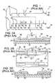
- FIGS. 6B , 6 C, and 6 Dshow for one implementation of the embodiment of FIG. 6A , respectively, the injection laser drive current waveform, the resultant injection laser pulse power profile, and an amplified laser pulse power profile replicating that of the injection laser pulse.
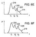
- FIGS. 6E and 6Fshow for another implementation of the embodiment of FIG. 6A , respectively, the injection laser drive current waveform and the resultant injection laser pulse power profile.
- FIG. 7is a partly schematic, simplified diagram of an embodiment of an exemplary system implemented with a diode-pumped, Q-switched Nd:YAG laser that is followed by an E-O gating device and a work piece positioner that cooperate with a laser processing control system for practicing the method of the present invention.
- FIGS. 3A and 3Bshow, respectively, the traditional laser pulse power profile and substantially square laser pulse profile used in the prior art.
- FIG. 3Cshows one embodiment of the invention that employs a specially tailored laser pulse power profile 60 c with a significant overshoot or “spike” 62 appearing at the beginning of the laser pulse.
- the peak power of the overshootis Pmax
- the average power of the laser pulseis Pmin.
- the amplitude of the overshootis defined as Pmax-Pmin.
- the width of the overshoot or “spike,” ⁇ tsis defined as the full duration time at the middle power point, Ps, between Pmax and Pmin.
- the peak power of the overshoot or the “spike,” Pmax,is preferably about 10% to about 50% over the average power of the laser pulse, Pmin.
- the width of the overshoot or “spike”, ⁇ ts,is preferably 10% to 50% of the duration of the laser pulse.
- the rise time of the spikeis typically shorter than about 5 ns, and preferably shorter than about 2 ns.
- FIG. 3Dshows another embodiment of the invention that employs a power profile 60 d with an overshoot or “spike” 64 appearing not at the beginning of but during the laser pulse.
- the overshoot or “spike”ends at time, t e , which is before the time, t 1 , when the link material is totally removed by the laser energy.
- the term “spike”is used throughout the remainder of the application to indicate a significant, transient increase in laser power, irrespective of when it occurs during the laser pulse.
- FIG. 3Eshows the conditions of the passivation layers after link 22 has been removed by a laser with laser pulse power profile 60 c or 60 d .
- Passivation layer 44 overlaying a top surface 70 of link 22has an opening 72 that extends beyond width 28 of link 22 by a relatively small amount, e.g., about the thickness of overlying passivation layer 44 .
- Intermediate passivation layer 48 material positioned adjacent side surfaces 52 of link 22 , passivation layer 46 underlying a bottom surface 74 of link 22 , and substrate 42are not appreciably damaged.
- FIG. 3Eshows an irregularly curved line 76 passing through portions of passivation layers 44 , 46 , and 48 surrounding the open area previously occupied by removed link 22 .
- Curved line 76represents typical damage to the passivation structure, specifically damage that extends by a certain amount, e.g., about 0.5 micron, from the region previously occupied by the link or becomes quite visible under a microscope. Typical damage also includes cracks in the passivation structure, which are not shown in the drawing figures.
- FIGS. 4-6show several preferred embodiments implementing laser pulse power profile tailoring and their associated specially tailored laser pulse power profiles employed to sever links 22 in accordance with the present invention.
- tailoring of the power profile of a laser pulseprovides it with sufficient peak power and energy of the pulse and proper duration to sever the link.
- the power profile and remaining duration of the laser pulseare tailored to impose no risk of damage to the substrate and neighboring structure of the link undergoing the process, even if the laser wavelength used is shorter than 1.3 ⁇ m, in the visible range, or in the UV range.
- each laser pulse 37severs a single link 22 .
- the references to laser pulse 37 and focused spot size 40in connection with the descriptions of preferred embodiments relate to emission of laser pulses and not to prior art power profiles associated with them).
- preferred ablation parameters of focused spot size 40 of laser pulses 37include laser energies of each laser pulse of between about 0.005 ⁇ J and about 10 ⁇ J, the duration of each laser pulse 37 is preferably shorter than about 40 ns and longer than about 1 ns, laser pulse repetition rate is greater than 1 Hz, more preferably within 10 KHz and 60 KHz or higher and may be a function of the speed of the positioning system 380 ( FIG. 7 ) and the distance between adjacent links 22 to be processed.
- the focused laser spot diameteris within the range of between about 0.5 ⁇ m and about 3 ⁇ m and preferably is about 40% to about 100% larger than the width of link 22 , depending on link width 28 , link pitch size 32 , link material, and other link structure and process considerations.
- the laser pulse power profiles 60 c and 60 dcan be specially tailored to have a significant leading edge overshoot 62 ( FIG. 3C ) at the beginning of the laser pulse or have one or two mid-pulse spikes 64 (one spike shown in FIG. 3D ) sometime within the duration of the laser pulse, before the link material is totally removed.
- Preferred timing of the power spikeis within an interval measured from the rising edge of the laser pulse power profile to 70% of the duration of the laser pulse power profile.
- FIG. 3Dshows laser pulse power profile 60 d in which the power level is relatively flat before and after pulse spike 64 .
- the laser pulse power profilecan have a changing power level before and after pulse spike 64 .
- Tailoring the laser pulse power profile in this mannerprovides from leading edge overshoot or mid-pulse spikes sufficient laser peak power and energy to facilitate the satisfactory removal of the link material and, upon removal of most of the link material, much lower laser pulse power to remove remaining link material and ensure reduced risk of damage to the silicon substrate and to the structure neighboring the link.
- such special tailoring of the laser power profiledelivers much better processing results and a wider process window and reduces risk of damage to the silicon substrate and to the structure neighboring the link.
- laser rail 110generates a shorter laser pulse 114 , shown in FIG. 4B
- laser rail 112generates a longer laser pulse 118 , shown in FIG. 4C .
- the synchronization of or delay time (t d ) between laser pulses 114 and 118is controlled by synchronizing electronics 120 .
- Laser pulses 114 and 118are combined by a beam combiner 130 after laser pulse 118 reflects off a mirror 131 and propagates through a waveplate 132 for polarization control purposes.
- FIG. 4Aspecial tailoring of the laser pulse power profile is accomplished by combining two laser pulses from two separate laser rails 110 and 112 .
- Laser rail 110generates a shorter laser pulse 114 , shown in FIG. 4B
- laser rail 112generates a longer laser pulse 118 , shown in FIG. 4C .
- the synchronization of or delay time (t d ) between laser pulses 114 and 118is controlled by synchronizing electronics 120 .
- the total laser pulse width of combined laser pulse 134can be either the sum of the widths of laser pulses 114 and 118 or the width of laser pulse 118 , depending on the delay time between laser pulses 114 and 118 .
- the widths of laser pulses 114 and 118can be optimized for the link processing based on the link structure.
- Combined laser pulse 134can be configured such that an additional power spike occurs at, for example, t a , after power spike 136 .
- the additional power spikewould preferably have a power value that is more than 5% of the average power of the combined laser pulse 134 .
- the timing of the spike 136 at time t pcan also be readily program controlled by synchronizing electronics 120 for the best link processing quality and yield. Skilled persons in the art will appreciate that, because they propagate from different laser rails and travel along different beam paths before combination by beam combiner 130 , laser pulses 114 and 118 can be manipulated to have different beam spot sizes to further facilitate the link processing.
- beam combiner 130combines laser pulses 114 and 118 , their polarization states are different from their original polarization states.
- the energy of laser pulse 114can be vertically polarized while the energy of laser pulse 118 can be horizontally polarized.
- An optional waveplate 140can be inserted along the propagation path of combined laser pulse 134 so that all of the laser energy is circularly polarized, if such a configuration delivers a better processing quality and yield for a particular link structure.
- an E-O gating device 150shapes the power profile of laser pulses propagating from a diode-pumped, Q-switched solid state laser 152 .
- Laser 152delivers multiple laser pulses 160 (one shown in Fig, 5 B), each with a relatively long laser pulse width at full width, half maximum (FWHM).
- the FWHM pulse widthcan be, for example, about 30ns to 50ns.
- Laser pulses 160propagate through E-O gating device 150 .
- the output laser pulse power profiledepends on the width and shape of a drive voltage pulse 162 delivered from drive electronics 164 and the delay time between laser pulse 160 and the drive voltage pulse 162 applied to E-O device 150 .
- the output laser pulsecan have an upwardly, substantially linearly inclined (increasing) power profile, as shown for laser pulse 166 c in FIG. 5C or a downwardly, substantially exponentially decreasing power profile with a higher peak at the very beginning of the laser pulse, as shown for laser pulse 166 d in FIG. 5D .
- the total power decline after the peakis more than about 10% of the average power of the laser output pulse.
- the width and shape of the voltage pulse itself applied to E-O device 150can be tailored to provide greater flexibility in tailoring the width and power profile of laser pulse 166 .
- a laser 200is composed of an injection laser 202 followed by an amplifier 204 .
- Injection laser 202can be a diode laser having a fast response time and delivering laser output at a laser wavelength that matches the gain spectrum of amplifier 204 .
- FIG. 6Bshows a specially tailored drive current pulse 206 delivered from driving electronics 208
- FIG. 6Cshows that an injection laser output pulse 210 propagating from injection laser 202 replicates the profile of drive current pulse 206 as a result of the fast response capability of injection laser 202 .
- Injection laser output pulse 210is delivered to laser power amplifier 204 , which is operating in an unsaturated state to amplify injection laser output pulse 210 and deliver an output pulse 212 without introducing significant distortion of the tailored laser pulse power profile, as shown in FIG. 6D .
- Output pulse 212is relatively flat after the occurrence of the power spike and before the falling edge of the laser pulse temporal power profile.
- the profile of drive current pulse 206can be readily programmed to any preferred profile in accordance with this invention.
- the gain requirement of amplifier 204depends on the laser pulse power available from injection laser 202 and the power of the laser output pulse 212 required for this invention.
- FIGS. 6E and 6Fshow, respectively, a drive current profile 214 and its replicated laser pulse power profile 216 produced in accordance with a different implementation of the third embodiment of FIG. 6A .
- Drive current profile 214is composed of a pulse with three time-displaced current spikes 218 , 220 , and 222 of decreasing values over time at t 1 , t 2 , t 3 , respectively.
- Current spikes 218 , 220 , and 222produce for laser pulse power profile 216 corresponding power spikes 224 , 226 , and 228 .
- Power spike 224represents an overshoot occurring at the rising edge of laser pulse power profile 216
- power spikes 226 and 228represent subsequent power spikes occurring during the pulse but before the target link material is completely removed.
- Power spikes 224 , 226 , and 228together form a composite power spike in the form of an oscillating wave with a power variation of over about 10% of the average power of the laser output pulse.
- the oscillating wavecan last from about one-half cycle to three cycles of duration within the duration of the laser pulse power profile.
- the period of the oscillation cycleis preferably between about 1 ns and about 15 ns.
- amplifier 204is a fiber laser amplifier.
- the length of the fiber, type of lasing dopant, doping level, and pumping levelcan be tailored to realize the required amplification gain.
- An exemplary laser 200can be a modification of a fiber laser manufactured by IMRA, America, Inc., Fremont, Calif. and IPG Photonics Corp., Oxford, Mass. Both IMRA and IPG manufacture laser devices that include a fast laser diode operating as the injection laser followed by a fiber power amplifier. The laser wavelength is tunable in the 1.06 ⁇ m to 1.1 ⁇ m range.
- the laser pulse shapeis substantially square shaped with a pulse width programmable from 5 ns to 20 ns, laser energy of 0.1 ⁇ J to 10 ⁇ J, and laser pulse repetition rate of about 20 KHz.
- the laser pulse power profilecan be tailored as described for the present invention.
- Another exemplary fiber laser manufactured by INO, Quebec, Canadaimplements a special technique to get the injection laser pulse from the fiber itself and then use the fiber to amplify the injection pulse. Its currently available version works at a laser wavelength of 1.57 ⁇ m, and its pulse profile is very similar to that shown in FIG. 6F . According to INO, it is not difficult to make a similar laser working at wavelength of 1.06 ⁇ m to 1.1 ⁇ m with a different tailored laser pulse profile.
- the preferred laser wavelengthsare in the spectral range from about 150 nm to about 2000 nm, and include, but are not limited to, 1.54, 1.3, 1.1-1.06, 1.05, 1.047, 1.03-0.75 ⁇ m or their second, third, fourth, or fifth harmonics from Nd:YAG, Nd:YLF, Nd:YVO 4 , Yb:YAG, Ti:Sapphire, and fiber lasers with different base materials and doping. Skilled persons will appreciate that lasers emitting output pulses at other suitable wavelengths are commercially available and could be employed.
- any of the second, third, or fourth harmonics of Nd:YAG (532 nm, 355 nm, 266 nm); Nd:YLF (524 nm, 349 nm, 262 nm); or the second harmonic of Ti:Sapphire (375 nm-425 nm)can be employed to preferably process certain types of links 22 and/or passivation layers 44 using appropriate well-known harmonic conversion techniques. Harmonic conversion processes are described in V. G. Dmitriev, et al., Handbook of Nonlinear Optical Crystals, 138-141, Springer-Verlag, New York, 1991 ISBN 3 ⁇ 540-53547-0.
- laser system 300is modeled herein only by way of example to a 1.064 ⁇ m Nd:YAG laser 302 .
- the Nd:YAG or other solid-state laser 302is preferably pumped by a laser diode 304 , the emission 306 of which is focused by lens components 308 into a laser resonator 310 .
- Laser resonator 310preferably includes a lasant 312 , a Q switch 314 , and an optional polarizer 315 positioned between resonator mirrors 316 and 318 along an optic axis 320 .
- An aperture 330may also be positioned between lasant 312 and mirror 318 .
- a laser output pulse 334propagates along optic axis 320 through mirror 318 , which functions as a partly reflective output coupler.
- laser pulse 334 propagating from laser 302is incident on an optional optical component or device 336 , such as a waveplate, a polarizer, or an isolator, and then undergoes the special intensity profile tailoring with an E-O gating device 340 , controlled by a subcontroller 342 .
- laser output 350 of gating device 340can be manipulated by a variety of conventional optical components 352 and 354 that are positioned along a beam path 356 .
- Components 352 and 354may include a beam expander or other laser optical components to collimate laser output 350 to produce a beam with useful propagation characteristics.
- One or more beam reflecting mirrors 358 , 360 , 362 , and 364 that are highly reflective at the laser wavelength desired, but highly transmissive at the unused wavelengths,are optionally employed so that only the desired laser wavelength will reach link structure 36 .
- a focusing lens 366preferably employs a single component or multicomponent lens system that focuses a collimated pulsed laser system output 368 to produce a focused spot size 40 that is greater than and thereby encompasses link width and is preferably less than 2 ⁇ m in diameter or smaller, depending on the link width 28 and the laser wavelength.
- a preferred beam positioning system 380composed of optical components 358 , 360 , 362 , and 364 is described in detail in U.S. Pat. No. 4,532,402 of Overbeck for Method and Apparatus for Positioning a Focused Beam on an Integrated Circuit.
- Beam positioning system 380preferably employs a laser controller 382 that controls at least two platforms or stages (stacked or split-axis) and coordinates with beam reflecting mirrors 358 , 360 , 362 , and 364 to target and focus laser system output 368 to a selected conductive link 22 on IC device or work piece 12 .
- Beam positioning system 380permits quick movement between links 22 on work piece 12 to effect unique link-severing operations on-the-fly, based on provided test or design data.
- the position datapreferably direct the focused laser spot 38 over work piece 12 to target link structure 36 with one laser pulse of laser system output 368 to remove link 22 .
- Laser system 300preferably severs on-the-fly with a single laser pulse 37 each of links 22 to be severed. Laser system 300 accomplishes this process without stopping beam positioning system 380 over any link 22 , so that high throughput is realized.
- Persons skilled in the artwill appreciate that such laser systems 300 equipped with conventional diode pumped, Q-switched solid-state lasers are commercially available and well known to skilled practitioners.
- Laser controller 382is provided with instructions concerning the proper process of the selected links.
- Laser controller 382may be influenced by timing data that synchronizes the firing of laser system 300 to the motion of the platforms such as described in U.S. Pat. No. 5,453,594 of Konecny for Radiation Beam Position and Emission Coordination System.
- laser controller 382is used for extracavity modulation of laser energy by an E-O device 340 and instructs subcontrollers 342 and 386 that control Q-switch 314 , E-O device 340 , and pumping diode 304 .
- link processing with laser pulse 37 of a specially tailored power profileoffers a wider processing window and a superior quality of severed links than does link processing with a laser pulse of conventional power profile.
- the overshoot at the beginning of the laser pulse and/or spike properly timed within the duration time of the laser pulseensures that an adequate amount of laser energy is coupled into the link structure within a proper time period before all the link material of the selected link is removed. This is accomplished with adequate processing margin for the inevitable variations of the link structure and the laser parameters themselves.
- the laser pulse poweris specially tailored to have much lower value compared to the peak power of the laser pulse, or the power of the overshoot and spike.
- this specially tailored laser pulse power profileensures less risk of damage to the neighboring structures and silicon substrate 42 .
- laser wavelengths shorter than the IR wavelengthscan also be used for the process with the added advantage of smaller laser beam spot size, even though the absorption of a silicon wafer at the shorter laser wavelengths is higher than that at the conventional IR wavelengths.
- This better link removal resolutionpermits links 22 to be positioned closer together, thereby increasing circuit density.
- link structures 36can have conventional sizes, the link width 28 can, for example, be less than or equal to about 0.5 ⁇ m.
- the versatility of better tailoring the laser pulse power profileoffers better flexibility in accommodating different passivation characteristics.
- Passivation layers 44 above or passivation layers 46 below links 22can be made with material other than the traditional materials or can be modified, if desired to be other than a typical height. This is so because the laser pulse can be tailored, thereby reducing the risk of damage to the underlying or neighboring passivation structure.
- wavelengths that are much shorter than about 1.06 ⁇ mcan be employed to produce critical spot size diameters 40 of less than about 2 ⁇ m center-to-center pitch 32 between links 22 .
- Links processed with laser pulses from shorter wavelength laserscan, therefore, have a substantially smaller center-to-center pitch 32 than that possible for links blown by a conventional IR laser beam-severing pulse.
- Link 22can, for example, be within a distance of 2.0 ⁇ m or less from other links 22 or adjacent circuit structures 34 .
- Overlying passivation layer 44may include any conventional passivation materials such as silicon dioxide (SiO 2 ) and silicon nitride (Si 3 N 4 ).
- Underlying passivation layer 46may include the same passivation material as or different passivation material(s) from overlying passivation layer 44 .
- underlying passivation layer 46 in target structures 36may comprise fragile materials, including but not limited to, materials formed from low K materials, low K dielectric materials, low K oxide-based dielectric materials, orthosilicate glasses (OSGs), fluorosilicate glasses, organosilicate glasses, tetraethylorthosilicate (TEOS)-based oxides, methyltriethoxyorthosilicate (MTEOS), propylene glycol monomethyl ether acetate (PGMEA), silicate esters, hydrogen silsesquioxane (HSQ), methyl silsesquioxane (MSQ), polyarylene ethers, benzocyclobutene (BCB), SiCOH, or SiCOH-derived film (such as “Black Diamond” sold by Applied Materials, Inc.), or spin on-based low K dielectric polymer (such as “SiLK” sold by Dow Chemical Company).
- fragile materialsincluding but not limited to, materials formed from low K materials, low K dielectric materials, low K oxide-based dielectric
- Underlying passivation layers 46 made from some of these materialsare more prone to crack when their targeted links 22 are blown or ablated by conventional single laser-pulse link-removal operations.
- Skilled personswill appreciate that SiO 2 , SiON, Si 3 N 4 , low K materials, low K dielectric materials, low K oxide-based dielectric materials, OSGs, fluorosilicate glasses, organosilicate glasses, HSQ, MSQ, BCB, SiLKTM, and Black DiamondTM are actual layer materials, and TEOS, MTEOS, and polyarylene ethers are semiconductor condensate precursor materials.
Landscapes
- Physics & Mathematics (AREA)
- Optics & Photonics (AREA)
- Engineering & Computer Science (AREA)
- Plasma & Fusion (AREA)
- Mechanical Engineering (AREA)
- Electromagnetism (AREA)
- General Physics & Mathematics (AREA)
- Computer Hardware Design (AREA)
- Microelectronics & Electronic Packaging (AREA)
- Power Engineering (AREA)
- Condensed Matter Physics & Semiconductors (AREA)
- Lasers (AREA)
- Laser Beam Processing (AREA)
- Dicing (AREA)
- Semiconductor Lasers (AREA)
Abstract
Description
Claims (37)
Priority Applications (2)
| Application Number | Priority Date | Filing Date | Title |
|---|---|---|---|
| US10/921,481US7348516B2 (en) | 2003-08-19 | 2004-08-18 | Methods of and laser systems for link processing using laser pulses with specially tailored power profiles |
| US12/052,577US20080203071A1 (en) | 2003-08-19 | 2008-03-20 | Link processing using laser pulses with specially tailored power profiles |
Applications Claiming Priority (2)
| Application Number | Priority Date | Filing Date | Title |
|---|---|---|---|
| US49663103P | 2003-08-19 | 2003-08-19 | |
| US10/921,481US7348516B2 (en) | 2003-08-19 | 2004-08-18 | Methods of and laser systems for link processing using laser pulses with specially tailored power profiles |
Related Child Applications (1)
| Application Number | Title | Priority Date | Filing Date |
|---|---|---|---|
| US12/052,577ContinuationUS20080203071A1 (en) | 2003-08-19 | 2008-03-20 | Link processing using laser pulses with specially tailored power profiles |
Publications (2)
| Publication Number | Publication Date |
|---|---|
| US20050067388A1 US20050067388A1 (en) | 2005-03-31 |
| US7348516B2true US7348516B2 (en) | 2008-03-25 |
Family
ID=34193377
Family Applications (3)
| Application Number | Title | Priority Date | Filing Date |
|---|---|---|---|
| US10/921,481Expired - LifetimeUS7348516B2 (en) | 2003-08-19 | 2004-08-18 | Methods of and laser systems for link processing using laser pulses with specially tailored power profiles |
| US10/921,765Expired - LifetimeUS7126746B2 (en) | 2003-08-19 | 2004-08-18 | Generating sets of tailored laser pulses |
| US12/052,577AbandonedUS20080203071A1 (en) | 2003-08-19 | 2008-03-20 | Link processing using laser pulses with specially tailored power profiles |
Family Applications After (2)
| Application Number | Title | Priority Date | Filing Date |
|---|---|---|---|
| US10/921,765Expired - LifetimeUS7126746B2 (en) | 2003-08-19 | 2004-08-18 | Generating sets of tailored laser pulses |
| US12/052,577AbandonedUS20080203071A1 (en) | 2003-08-19 | 2008-03-20 | Link processing using laser pulses with specially tailored power profiles |
Country Status (9)
| Country | Link |
|---|---|
| US (3) | US7348516B2 (en) |
| JP (2) | JP4384665B2 (en) |
| KR (2) | KR101123911B1 (en) |
| CN (2) | CN100593292C (en) |
| CA (2) | CA2535623A1 (en) |
| DE (2) | DE112004001527T5 (en) |
| GB (2) | GB2420307B (en) |
| TW (2) | TWI354417B (en) |
| WO (2) | WO2005018064A2 (en) |
Cited By (26)
| Publication number | Priority date | Publication date | Assignee | Title |
|---|---|---|---|---|
| US20050100062A1 (en)* | 2003-06-30 | 2005-05-12 | Electro Scientific Industries, Inc. | High energy pulse suppression method |
| US20060028655A1 (en)* | 2001-03-29 | 2006-02-09 | Gsil Lumonics Corporation | Methods and systems for precisely relatively positioning a waist of a pulsed laser beam and method and system for controlling energy delivered to a target structure |
| US20090245302A1 (en)* | 2008-03-31 | 2009-10-01 | Electro Scientific Industries, Inc. | Methods and systems for dynamically generating tailored laser pulses |
| US20090323741A1 (en)* | 2008-06-27 | 2009-12-31 | Institut National D'optique | Digital laser pulse shaping module and system |
| US20100118899A1 (en)* | 2008-11-10 | 2010-05-13 | Electro Scientific Industries, Inc. | Generating laser pulses of prescribed pulse shapes programmed through combination of separate electrical and optical modulators |
| US20100177794A1 (en)* | 2009-01-15 | 2010-07-15 | Electro Scientific Industries, Inc. | Pulse temporal programmable ultrafast burst mode laser for micromachining |
| US20100246611A1 (en)* | 2009-03-27 | 2010-09-30 | Electro Scientific Industries, Inc. | Laser micromachining with tailored bursts of short laser pulses |
| US20100276405A1 (en)* | 2008-03-31 | 2010-11-04 | Electro Scientific Industries, Inc. | Laser systems and methods using triangular-shaped tailored laser pulses for selected target classes |
| US20100301026A1 (en)* | 2006-09-21 | 2010-12-02 | Semiconductor Energy Laboratory Co., Ltd. | Manufacturing Method of Semiconductor Device and Laser Processing Apparatus |
| US20100316072A1 (en)* | 2008-06-27 | 2010-12-16 | Institut National D'optique | Methods for stabilizing the output of a pulsed laser system having pulse shaping capabilities |
| US20100316071A1 (en)* | 2009-06-10 | 2010-12-16 | Kimberlin Dwight | Laser device and method |
| US20120061356A1 (en)* | 2009-08-11 | 2012-03-15 | Hamamatsu Photonics K.K. | Laser machining device and laser machining method |
| US20120195331A1 (en)* | 2007-05-18 | 2012-08-02 | Gsi Lumonics Corporation | Laser processing of conductive links |
| US8263903B2 (en) | 2010-05-18 | 2012-09-11 | Institut National D'optique | Method for stablizing an output of a pulsed laser system using pulse shaping |
| US20120250707A1 (en)* | 2011-03-31 | 2012-10-04 | Electro Scientific Industries, Inc. | Stabilization of pulsed mode seed lasers |
| US8571077B2 (en) | 2010-08-31 | 2013-10-29 | First Solar, Inc. | System and method for laser modulation |
| US8598490B2 (en) | 2008-03-31 | 2013-12-03 | Electro Scientific Industries, Inc. | Methods and systems for laser processing a workpiece using a plurality of tailored laser pulse shapes |
| US8599891B2 (en) | 2011-03-21 | 2013-12-03 | Soreq Nuclear Research Center | Laser diode driver |
| US8842358B2 (en) | 2012-08-01 | 2014-09-23 | Gentex Corporation | Apparatus, method, and process with laser induced channel edge |
| US20150070753A1 (en)* | 2013-09-09 | 2015-03-12 | Coherent Kaiserslautern GmbH | Multi-stage mopa with first-pulse suppression |
| US9036247B2 (en) | 2011-07-05 | 2015-05-19 | Electro Scientific Industries, Inc. | Systems and methods for providing temperature stability of acousto-optic beam deflectors and acousto-optic modulators during use |
| US9054494B2 (en) | 2011-07-11 | 2015-06-09 | V Technology Co., Ltd. | Pulsed laser oscillator and method for controlling pulsed laser oscillation |
| US9155140B2 (en) | 2012-06-07 | 2015-10-06 | Gabriel Yavor | Optical waveform generator |
| US9300105B2 (en) | 2011-09-14 | 2016-03-29 | Fianium Ltd. | Methods and apparatus pertaining to picosecond pulsed fiber based lasers |
| US9425334B2 (en) | 2010-09-06 | 2016-08-23 | Fianium Ltd | Methods and apparatus for patterning photovoltaic devices and materials for use with such devices |
| US11539190B2 (en) | 2016-09-02 | 2022-12-27 | Kyushu University, National University Corporation | Continuous-wave organic thin-film distributed feedback laser and electrically driven organic semiconductor laser diode |
Families Citing this family (101)
| Publication number | Priority date | Publication date | Assignee | Title |
|---|---|---|---|---|
| US7838794B2 (en) | 1999-12-28 | 2010-11-23 | Gsi Group Corporation | Laser-based method and system for removing one or more target link structures |
| US6281471B1 (en)* | 1999-12-28 | 2001-08-28 | Gsi Lumonics, Inc. | Energy-efficient, laser-based method and system for processing target material |
| US7723642B2 (en) | 1999-12-28 | 2010-05-25 | Gsi Group Corporation | Laser-based system for memory link processing with picosecond lasers |
| US7671295B2 (en) | 2000-01-10 | 2010-03-02 | Electro Scientific Industries, Inc. | Processing a memory link with a set of at least two laser pulses |
| US7563695B2 (en)* | 2002-03-27 | 2009-07-21 | Gsi Group Corporation | Method and system for high-speed precise laser trimming and scan lens for use therein |
| US6951995B2 (en)* | 2002-03-27 | 2005-10-04 | Gsi Lumonics Corp. | Method and system for high-speed, precise micromachining an array of devices |
| US7361171B2 (en) | 2003-05-20 | 2008-04-22 | Raydiance, Inc. | Man-portable optical ablation system |
| US7367969B2 (en)* | 2003-08-11 | 2008-05-06 | Raydiance, Inc. | Ablative material removal with a preset removal rate or volume or depth |
| US8921733B2 (en) | 2003-08-11 | 2014-12-30 | Raydiance, Inc. | Methods and systems for trimming circuits |
| US9022037B2 (en) | 2003-08-11 | 2015-05-05 | Raydiance, Inc. | Laser ablation method and apparatus having a feedback loop and control unit |
| US8173929B1 (en) | 2003-08-11 | 2012-05-08 | Raydiance, Inc. | Methods and systems for trimming circuits |
| US7173212B1 (en)* | 2004-02-13 | 2007-02-06 | Semak Vladimir V | Method and apparatus for laser cutting and drilling of semiconductor materials and glass |
| US7486705B2 (en)* | 2004-03-31 | 2009-02-03 | Imra America, Inc. | Femtosecond laser processing system with process parameters, controls and feedback |
| US7491909B2 (en)* | 2004-03-31 | 2009-02-17 | Imra America, Inc. | Pulsed laser processing with controlled thermal and physical alterations |
| US7885311B2 (en)* | 2007-03-27 | 2011-02-08 | Imra America, Inc. | Beam stabilized fiber laser |
| US20060128073A1 (en)* | 2004-12-09 | 2006-06-15 | Yunlong Sun | Multiple-wavelength laser micromachining of semiconductor devices |
| US7289549B2 (en) | 2004-12-09 | 2007-10-30 | Electro Scientific Industries, Inc. | Lasers for synchronized pulse shape tailoring |
| US20060151704A1 (en)* | 2004-12-30 | 2006-07-13 | Cordingley James J | Laser-based material processing methods, system and subsystem for use therein for precision energy control |
| US20060191884A1 (en)* | 2005-01-21 | 2006-08-31 | Johnson Shepard D | High-speed, precise, laser-based material processing method and system |
| US8135050B1 (en) | 2005-07-19 | 2012-03-13 | Raydiance, Inc. | Automated polarization correction |
| US7444049B1 (en) | 2006-01-23 | 2008-10-28 | Raydiance, Inc. | Pulse stretcher and compressor including a multi-pass Bragg grating |
| US9130344B2 (en)* | 2006-01-23 | 2015-09-08 | Raydiance, Inc. | Automated laser tuning |
| US8232687B2 (en) | 2006-04-26 | 2012-07-31 | Raydiance, Inc. | Intelligent laser interlock system |
| US8189971B1 (en) | 2006-01-23 | 2012-05-29 | Raydiance, Inc. | Dispersion compensation in a chirped pulse amplification system |
| DE502006009433D1 (en)* | 2006-03-03 | 2011-06-16 | Fraunhofer Ges Forschung | Device for the laser processing of a cornea |
| US20070215575A1 (en)* | 2006-03-15 | 2007-09-20 | Bo Gu | Method and system for high-speed, precise, laser-based modification of one or more electrical elements |
| US7822347B1 (en) | 2006-03-28 | 2010-10-26 | Raydiance, Inc. | Active tuning of temporal dispersion in an ultrashort pulse laser system |
| US8198566B2 (en)* | 2006-05-24 | 2012-06-12 | Electro Scientific Industries, Inc. | Laser processing of workpieces containing low-k dielectric material |
| US8084706B2 (en) | 2006-07-20 | 2011-12-27 | Gsi Group Corporation | System and method for laser processing at non-constant velocities |
| JP2009545177A (en) | 2006-07-27 | 2009-12-17 | エレクトロ サイエンティフィック インダストリーズ インコーポレーテッド | Tandem optical amplifier |
| JP4954836B2 (en)* | 2006-09-21 | 2012-06-20 | 株式会社半導体エネルギー研究所 | Method for manufacturing semiconductor device |
| US8223522B2 (en)* | 2006-09-25 | 2012-07-17 | Flextronics Ap, Llc | Bi-directional regulator for regulating power |
| US7428253B2 (en)* | 2006-09-29 | 2008-09-23 | Pyrophotonics Lasers Inc. | Method and system for a pulsed laser source emitting shaped optical waveforms |
| DE102006046790B4 (en)* | 2006-10-02 | 2014-01-02 | Infineon Technologies Ag | Integrated component and method for separating an electrically conductive connection |
| US8026158B2 (en)* | 2007-06-01 | 2011-09-27 | Electro Scientific Industries, Inc. | Systems and methods for processing semiconductor structures using laser pulses laterally distributed in a scanning window |
| GB0713265D0 (en)* | 2007-07-09 | 2007-08-15 | Spi Lasers Uk Ltd | Apparatus and method for laser processing a material |
| US8168920B2 (en)* | 2007-09-11 | 2012-05-01 | Shibuya Kogyo Co., Ltd. | Bonding device |
| KR101310243B1 (en)* | 2007-09-19 | 2013-09-24 | 지에스아이 그룹 코포레이션 | Link processing with high speed beam deflection |
| US7903326B2 (en) | 2007-11-30 | 2011-03-08 | Radiance, Inc. | Static phase mask for high-order spectral phase control in a hybrid chirped pulse amplifier system |
| US20090141750A1 (en)* | 2007-12-03 | 2009-06-04 | Electro Scientific Industries, Inc. | Systems and methods for link processing with ultrafast and nanosecond laser pulses |
| US20090200675A1 (en) | 2008-02-11 | 2009-08-13 | Thomas Goebel | Passivated Copper Chip Pads |
| US7982161B2 (en)* | 2008-03-24 | 2011-07-19 | Electro Scientific Industries, Inc. | Method and apparatus for laser drilling holes with tailored laser pulses |
| US20090246413A1 (en)* | 2008-03-27 | 2009-10-01 | Imra America, Inc. | Method for fabricating thin films |
| US7817686B2 (en)* | 2008-03-27 | 2010-10-19 | Electro Scientific Industries, Inc. | Laser micromachining using programmable pulse shapes |
| US20090246530A1 (en)* | 2008-03-27 | 2009-10-01 | Imra America, Inc. | Method For Fabricating Thin Films |
| US8178818B2 (en)* | 2008-03-31 | 2012-05-15 | Electro Scientific Industries, Inc. | Photonic milling using dynamic beam arrays |
| US7982160B2 (en) | 2008-03-31 | 2011-07-19 | Electro Scientific Industries, Inc. | Photonic clock stabilized laser comb processing |
| WO2009137182A2 (en) | 2008-03-31 | 2009-11-12 | Electro Scientific Industries, Inc. | Combining multiple laser beams to form high repetition rate, high average power polarized laser beam |
| JP2009274365A (en)* | 2008-05-15 | 2009-11-26 | Sharp Corp | Printing method, printing apparatus, printing plate used in it, and pattern film |
| US8031042B2 (en)* | 2008-05-28 | 2011-10-04 | Flextronics Ap, Llc | Power converter magnetic devices |
| JP5589318B2 (en)* | 2008-08-11 | 2014-09-17 | 住友電気工業株式会社 | Laser marking method |
| US8125704B2 (en)* | 2008-08-18 | 2012-02-28 | Raydiance, Inc. | Systems and methods for controlling a pulsed laser by combining laser signals |
| JP5332462B2 (en)* | 2008-09-29 | 2013-11-06 | ソニー株式会社 | Short pulse light source, laser beam emitting method, optical device, optical disk device, and optical pickup |
| JP5338234B2 (en)* | 2008-09-30 | 2013-11-13 | ソニー株式会社 | Short pulse light source, laser beam emitting method, optical device, optical disk device, and optical pickup |
| US8246714B2 (en)* | 2009-01-30 | 2012-08-21 | Imra America, Inc. | Production of metal and metal-alloy nanoparticles with high repetition rate ultrafast pulsed laser ablation in liquids |
| US8609512B2 (en)* | 2009-03-27 | 2013-12-17 | Electro Scientific Industries, Inc. | Method for laser singulation of chip scale packages on glass substrates |
| US8411352B2 (en)* | 2009-08-17 | 2013-04-02 | Coherent, Inc. | Pulsed fiber-MOPA with widely-variable pulse-duration |
| US8890025B2 (en)* | 2009-09-24 | 2014-11-18 | Esi-Pyrophotonics Lasers Inc. | Method and apparatus to scribe thin film layers of cadmium telluride solar cells |
| KR20120098623A (en)* | 2009-09-24 | 2012-09-05 | 이에스아이-파이로포토닉스 레이저스, 인코포레이티드 | Method and apparatus to scribe a line in a thin film material using a burst of laser pulses with beneficial pulse shape |
| KR20120113245A (en)* | 2009-12-30 | 2012-10-12 | 지에스아이 그룹 코포레이션 | Link processing with high speed beam deflection |
| US8858676B2 (en)* | 2010-02-10 | 2014-10-14 | Imra America, Inc. | Nanoparticle production in liquid with multiple-pulse ultrafast laser ablation |
| US8540173B2 (en)* | 2010-02-10 | 2013-09-24 | Imra America, Inc. | Production of fine particles of functional ceramic by using pulsed laser |
| US20110192450A1 (en)* | 2010-02-10 | 2011-08-11 | Bing Liu | Method for producing nanoparticle solutions based on pulsed laser ablation for fabrication of thin film solar cells |
| US8379679B2 (en) | 2010-02-11 | 2013-02-19 | Electro Scientific Industries, Inc. | Method and apparatus for reliably laser marking articles |
| US8451873B2 (en) | 2010-02-11 | 2013-05-28 | Electro Scientific Industries, Inc. | Method and apparatus for reliably laser marking articles |
| US8379678B2 (en)* | 2010-02-11 | 2013-02-19 | Electro Scientific Industries, Inc. | Method and apparatus for reliably laser marking articles |
| US8586873B2 (en)* | 2010-02-23 | 2013-11-19 | Flextronics Ap, Llc | Test point design for a high speed bus |
| EP2392429A1 (en)* | 2010-06-03 | 2011-12-07 | Lasag Ag | Pulsed laser machining method and installation, in particular for welding, with variation of power within each pulse |
| US8211731B2 (en)* | 2010-06-07 | 2012-07-03 | Sunpower Corporation | Ablation of film stacks in solar cell fabrication processes |
| US8389895B2 (en) | 2010-06-25 | 2013-03-05 | Electro Scientifix Industries, Inc. | Method and apparatus for reliably laser marking articles |
| TWI549836B (en)* | 2010-08-30 | 2016-09-21 | 伊雷克托科學工業股份有限公司 | Method and apparatus for reliably laser marking articles |
| KR20140018183A (en) | 2010-09-16 | 2014-02-12 | 레이디안스, 아이엔씨. | Laser based processing of layered materials |
| CN103222133A (en)* | 2010-11-17 | 2013-07-24 | 松下电器产业株式会社 | Laser light source, laser processing device, and semiconductor processing method |
| CN103228399B (en)* | 2011-03-10 | 2016-04-13 | 伊雷克托科学工业股份有限公司 | Method and apparatus for reliably laser marking items |
| JP2012213802A (en)* | 2011-04-01 | 2012-11-08 | Esi-Pyrophotonics Lasers Inc | Method and apparatus for scribing thin film layer of cadmium telluride solar cell |
| WO2012165481A1 (en)* | 2011-06-03 | 2012-12-06 | 住友電気工業株式会社 | Pulse light generating method |
| JP5923884B2 (en)* | 2011-07-14 | 2016-05-25 | 株式会社ブイ・テクノロジー | Pulse laser oscillator |
| JP5923885B2 (en)* | 2011-07-14 | 2016-05-25 | 株式会社ブイ・テクノロジー | Pulse laser oscillator and pulse laser oscillation control method |
| EP2804716B1 (en)* | 2012-01-20 | 2018-04-18 | ROFIN-BAASEL Lasertech GmbH & Co. KG | Method and device for processing materials using a pulsed laser beam generated by a fiber laser |
| CN102605333B (en)* | 2012-03-28 | 2013-11-27 | 中国矿业大学 | Preparation method of tantalum oxide film with high laser damage threshold under high temperature environment |
| US20140015170A1 (en)* | 2012-07-10 | 2014-01-16 | Electro Scientific Industries, Inc. | Method and apparatus for marking an article |
| US9019592B2 (en)* | 2013-02-01 | 2015-04-28 | Institut National D'optique | System and method for emitting optical pulses in view of a variable external trigger signal |
| US20140227820A1 (en)* | 2013-02-08 | 2014-08-14 | Applied Materials, Inc. | Passivation layer removal by delivering a split laser pulse |
| CN105102174B (en)* | 2013-03-15 | 2017-05-31 | 伊雷克托科学工业股份有限公司 | Beam Positioner Controlled Based on Laser Radiation |
| FR3004848B1 (en)* | 2013-04-22 | 2015-06-05 | Centre Nat Rech Scient | METHOD OF MODIFYING THE VALUE OF AN ELECTRIC RESISTANCE COMPRISING A FERROMAGNETIC MATERIAL |
| US10239155B1 (en)* | 2014-04-30 | 2019-03-26 | The Boeing Company | Multiple laser beam processing |
| EP3023073B1 (en)* | 2014-11-24 | 2021-01-27 | Fotona d.o.o. | Laser system for tissue ablation |
| US20160279737A1 (en) | 2015-03-26 | 2016-09-29 | Pratt & Whitney Canada Corp. | Laser drilling through multi-layer components |
| KR101787483B1 (en)* | 2016-02-16 | 2017-10-18 | 주식회사 이오테크닉스 | Laser pulse controlling apparatus and method for controlling laser pulses |
| JP6238185B2 (en)* | 2016-05-18 | 2017-11-29 | 株式会社アマダホールディングス | Laser cutting processing method, laser cutting processing product, thermal cutting processing method, thermal cutting processing product, surface-treated steel plate, laser cutting method and laser processing head of plated steel plate |
| US11919103B2 (en)* | 2016-07-22 | 2024-03-05 | Illinois Tool Works Inc. | Laser welding, cladding, and/or additive manufacturing systems and methods of laser welding, cladding, and/or additive manufacturing |
| TWI846301B (en)* | 2016-09-02 | 2024-06-21 | 國立大學法人九州大學 | Simulation modeling method for an organic laser device, program for performing the simulation modeling method, and method for manufacturing an organic laser device |
| CN109996640B (en)* | 2016-11-18 | 2021-09-03 | Ipg光子公司 | Laser system and method for processing materials |
| US11183815B2 (en) | 2017-02-07 | 2021-11-23 | Koala Tech Inc. | Current-injection organic semiconductor laser diode, meihod for producing same and program |
| US11209478B2 (en)* | 2018-04-03 | 2021-12-28 | Applied Materials, Inc. | Pulse system verification |
| CN111345893A (en)* | 2018-12-24 | 2020-06-30 | 爱科凯能科技(北京)股份有限公司 | Laser medical treatment method and apparatus |
| FR3092442B1 (en)* | 2019-02-04 | 2022-12-30 | Amplitude Systemes | Laser system with temporal superposition of pulses |
| JP7492726B2 (en)* | 2020-03-17 | 2024-05-30 | スパークリングフォトン株式会社 | Pulsed laser oscillator |
| US11990729B2 (en)* | 2020-03-23 | 2024-05-21 | Lumentum Operations Llc | Shaping pulses using a multi-section optical load |
| US11870215B2 (en)* | 2020-03-23 | 2024-01-09 | Lumentum Operations Llc | Reconfigurable laser pulse generating circuit |
| CN112676267B (en)* | 2020-12-10 | 2022-05-31 | 中国科学院半导体研究所 | Pulse laser cleaning method |
Citations (31)
| Publication number | Priority date | Publication date | Assignee | Title |
|---|---|---|---|---|
| US3747019A (en) | 1970-07-16 | 1973-07-17 | Union Carbide Corp | Method and means for stabilizing the amplitude and repetition frequency of a repetitively q-switched laser |
| US3879686A (en) | 1973-09-20 | 1975-04-22 | Us Air Force | Laser system for producing variable duration short pulses |
| US4483005A (en) | 1981-09-24 | 1984-11-13 | Teradyne, Inc. | Affecting laser beam pulse width |
| US5265114A (en) | 1992-09-10 | 1993-11-23 | Electro Scientific Industries, Inc. | System and method for selectively laser processing a target structure of one or more materials of a multimaterial, multilayer device |
| US5307369A (en) | 1992-05-06 | 1994-04-26 | Electrox, Inc. | Laser beam combination system |
| US5319195A (en) | 1991-04-02 | 1994-06-07 | Lumonics Ltd. | Laser system method and apparatus for performing a material processing operation and for indicating the state of the operation |
| US5339764A (en) | 1992-05-04 | 1994-08-23 | Wabco Standard Gmbh | Device for optically indicating the pressure of a medium |
| US5756924A (en) | 1995-09-28 | 1998-05-26 | The Regents Of The University Of California | Multiple laser pulse ignition method and apparatus |
| US5998759A (en) | 1996-12-24 | 1999-12-07 | General Scanning, Inc. | Laser processing |
| US6025256A (en) | 1997-01-06 | 2000-02-15 | Electro Scientific Industries, Inc. | Laser based method and system for integrated circuit repair or reconfiguration |
| US6057180A (en) | 1998-06-05 | 2000-05-02 | Electro Scientific Industries, Inc. | Method of severing electrically conductive links with ultraviolet laser output |
| US6169014B1 (en) | 1998-09-04 | 2001-01-02 | U.S. Philips Corporation | Laser crystallization of thin films |
| US6210401B1 (en) | 1991-08-02 | 2001-04-03 | Shui T. Lai | Method of, and apparatus for, surgery of the cornea |
| US6252195B1 (en) | 1999-04-26 | 2001-06-26 | Ethicon, Inc. | Method of forming blind holes in surgical needles using a diode pumped Nd-YAG laser |
| US6281471B1 (en) | 1999-12-28 | 2001-08-28 | Gsi Lumonics, Inc. | Energy-efficient, laser-based method and system for processing target material |
| US20010050931A1 (en) | 2000-06-09 | 2001-12-13 | Sumitomo Heavy Industries, Ltd | Laser processing apparatus and method |
| US20020003130A1 (en) | 2000-01-10 | 2002-01-10 | Yunlong Sun | Laser system and method for processing a memory link with a burst of laser pulses having ultrashort pulse widths |
| US6339604B1 (en) | 1998-06-12 | 2002-01-15 | General Scanning, Inc. | Pulse control in laser systems |
| US6340806B1 (en) | 1999-12-28 | 2002-01-22 | General Scanning Inc. | Energy-efficient method and system for processing target material using an amplified, wavelength-shifted pulse train |
| US6346686B1 (en) | 1999-04-14 | 2002-02-12 | Hughes Electronics Corporation | Apparatus and method for enhanced laser machining by optimization of pulse duration and spacing |
| US6433306B1 (en)* | 1997-02-19 | 2002-08-13 | Jds Uniphase Corp. | Semiconductor laser high power amplifier system for materials processing |
| US6462307B1 (en)* | 1999-07-12 | 2002-10-08 | Mdc Max Datwyler Ag Bleienbach | Process for producing an intensity distribution over a working laser beam and a device for this purpose |
| US20020167581A1 (en)* | 2001-03-29 | 2002-11-14 | Cordingley James J. | Methods and systems for thermal-based laser processing a multi-material device |
| US6541731B2 (en) | 2000-01-25 | 2003-04-01 | Aculight Corporation | Use of multiple laser sources for rapid, flexible machining and production of vias in multi-layered substrates |
| US20030151053A1 (en) | 2000-01-10 | 2003-08-14 | Yunlong Sun | Processing a memory link with a set of at least two laser pulses |
| US20030222324A1 (en) | 2000-01-10 | 2003-12-04 | Yunlong Sun | Laser systems for passivation or link processing with a set of laser pulses |
| US20030222330A1 (en) | 2000-01-10 | 2003-12-04 | Yunlong Sun | Passivation processing over a memory link |
| EP1422796A2 (en) | 2002-11-21 | 2004-05-26 | New Wave Research | Dual head laser system with intracavity polarization and particle image velocimetry system using the same |
| US20040134896A1 (en) | 1999-12-28 | 2004-07-15 | Bo Gu | Laser-based method and system for memory link processing with picosecond lasers |
| US20040134894A1 (en) | 1999-12-28 | 2004-07-15 | Bo Gu | Laser-based system for memory link processing with picosecond lasers |
| WO2004098003A1 (en) | 2003-04-29 | 2004-11-11 | Southampton Photonics Limited | Laser apparatus for material processing |
Family Cites Families (13)
| Publication number | Priority date | Publication date | Assignee | Title |
|---|---|---|---|---|
| US151053A (en)* | 1874-05-19 | Improvement in thill-couplings | ||
| US134894A (en)* | 1873-01-14 | Improvement in wheels for vehicles | ||
| US134896A (en)* | 1873-01-14 | Improvement in bows for chair-backs | ||
| US167581A (en)* | 1875-09-07 | Improvement in pen-holders | ||
| US222330A (en)* | 1879-12-02 | Improvement in spinning-frames | ||
| US222324A (en)* | 1879-12-02 | Improvement in snap-hooks | ||
| US4806952A (en)* | 1986-07-04 | 1989-02-21 | Hitachi, Ltd. | Information recording apparatus for recording/reproducing information by irradiating an information recording medium with an energy beam |
| US5841099A (en)* | 1994-07-18 | 1998-11-24 | Electro Scientific Industries, Inc. | Method employing UV laser pulses of varied energy density to form depthwise self-limiting blind vias in multilayered targets |
| US5539764A (en)* | 1994-08-24 | 1996-07-23 | Jamar Technologies Co. | Laser generated X-ray source |
| US6449294B1 (en)* | 1999-07-26 | 2002-09-10 | Pls Liquidating Llc | Single dominant spike output erbium laser |
| US20020156758A1 (en)* | 2001-02-22 | 2002-10-24 | Remi Cote | System and method for dynamic addition and removal of object interfaces |
| US6784399B2 (en)* | 2001-05-09 | 2004-08-31 | Electro Scientific Industries, Inc. | Micromachining with high-energy, intra-cavity Q-switched CO2 laser pulses |
| US7557977B2 (en)* | 2003-06-03 | 2009-07-07 | Kilolambda Tech Ltd | Laser pulse generator |
- 2004
- 2004-08-18KRKR1020067003155Apatent/KR101123911B1/ennot_activeExpired - Fee Related
- 2004-08-18CNCN200480023900Apatent/CN100593292C/ennot_activeExpired - Fee Related
- 2004-08-18JPJP2006524039Apatent/JP4384665B2/ennot_activeExpired - Fee Related
- 2004-08-18GBGB0604738Apatent/GB2420307B/ennot_activeExpired - Fee Related
- 2004-08-18GBGB0603152Apatent/GB2421837B/ennot_activeExpired - Fee Related
- 2004-08-18WOPCT/US2004/026928patent/WO2005018064A2/enactiveApplication Filing
- 2004-08-18USUS10/921,481patent/US7348516B2/ennot_activeExpired - Lifetime
- 2004-08-18JPJP2006524052Apatent/JP4391524B2/ennot_activeExpired - Fee Related
- 2004-08-18KRKR1020067003152Apatent/KR100804253B1/ennot_activeExpired - Fee Related
- 2004-08-18DEDE112004001527Tpatent/DE112004001527T5/ennot_activeCeased
- 2004-08-18CACA002535623Apatent/CA2535623A1/ennot_activeAbandoned
- 2004-08-18DEDE112004001540Tpatent/DE112004001540T5/ennot_activeWithdrawn
- 2004-08-18CACA002535706Apatent/CA2535706A1/ennot_activeAbandoned
- 2004-08-18CNCNB2004800238993Apatent/CN100563903C/ennot_activeExpired - Fee Related
- 2004-08-18WOPCT/US2004/026977patent/WO2005016586A2/enactiveApplication Filing
- 2004-08-18USUS10/921,765patent/US7126746B2/ennot_activeExpired - Lifetime
- 2004-08-19TWTW093124919Apatent/TWI354417B/ennot_activeIP Right Cessation
- 2004-08-19TWTW093124918Apatent/TWI260121B/ennot_activeIP Right Cessation
- 2008
- 2008-03-20USUS12/052,577patent/US20080203071A1/ennot_activeAbandoned
Patent Citations (44)
| Publication number | Priority date | Publication date | Assignee | Title |
|---|---|---|---|---|
| US3747019A (en) | 1970-07-16 | 1973-07-17 | Union Carbide Corp | Method and means for stabilizing the amplitude and repetition frequency of a repetitively q-switched laser |
| US3879686A (en) | 1973-09-20 | 1975-04-22 | Us Air Force | Laser system for producing variable duration short pulses |
| US4483005A (en) | 1981-09-24 | 1984-11-13 | Teradyne, Inc. | Affecting laser beam pulse width |
| US5319195A (en) | 1991-04-02 | 1994-06-07 | Lumonics Ltd. | Laser system method and apparatus for performing a material processing operation and for indicating the state of the operation |
| US6210401B1 (en) | 1991-08-02 | 2001-04-03 | Shui T. Lai | Method of, and apparatus for, surgery of the cornea |
| US5339764A (en) | 1992-05-04 | 1994-08-23 | Wabco Standard Gmbh | Device for optically indicating the pressure of a medium |
| US5307369A (en) | 1992-05-06 | 1994-04-26 | Electrox, Inc. | Laser beam combination system |
| US5265114A (en) | 1992-09-10 | 1993-11-23 | Electro Scientific Industries, Inc. | System and method for selectively laser processing a target structure of one or more materials of a multimaterial, multilayer device |
| US5473624A (en) | 1992-09-10 | 1995-12-05 | Electro Scientific Industries, Inc. | Laser system and method for selectively severing links |
| US5265114C1 (en) | 1992-09-10 | 2001-08-21 | Electro Scient Ind Inc | System and method for selectively laser processing a target structure of one or more materials of a multimaterial multilayer device |
| US5756924A (en) | 1995-09-28 | 1998-05-26 | The Regents Of The University Of California | Multiple laser pulse ignition method and apparatus |
| US5998759A (en) | 1996-12-24 | 1999-12-07 | General Scanning, Inc. | Laser processing |
| US6878899B2 (en) | 1996-12-24 | 2005-04-12 | Gsi Lumonics Corp. | Laser processing |
| US6025256A (en) | 1997-01-06 | 2000-02-15 | Electro Scientific Industries, Inc. | Laser based method and system for integrated circuit repair or reconfiguration |
| US6433306B1 (en)* | 1997-02-19 | 2002-08-13 | Jds Uniphase Corp. | Semiconductor laser high power amplifier system for materials processing |
| US6057180A (en) | 1998-06-05 | 2000-05-02 | Electro Scientific Industries, Inc. | Method of severing electrically conductive links with ultraviolet laser output |
| US6339604B1 (en) | 1998-06-12 | 2002-01-15 | General Scanning, Inc. | Pulse control in laser systems |
| US6169014B1 (en) | 1998-09-04 | 2001-01-02 | U.S. Philips Corporation | Laser crystallization of thin films |
| US6346686B1 (en) | 1999-04-14 | 2002-02-12 | Hughes Electronics Corporation | Apparatus and method for enhanced laser machining by optimization of pulse duration and spacing |
| US6252195B1 (en) | 1999-04-26 | 2001-06-26 | Ethicon, Inc. | Method of forming blind holes in surgical needles using a diode pumped Nd-YAG laser |
| US6462307B1 (en)* | 1999-07-12 | 2002-10-08 | Mdc Max Datwyler Ag Bleienbach | Process for producing an intensity distribution over a working laser beam and a device for this purpose |
| US20040134896A1 (en) | 1999-12-28 | 2004-07-15 | Bo Gu | Laser-based method and system for memory link processing with picosecond lasers |
| US20050150879A1 (en) | 1999-12-28 | 2005-07-14 | Gsi Lumonics Corporation | Laser-based method and system for memory link processing with picosecond lasers |
| US6281471B1 (en) | 1999-12-28 | 2001-08-28 | Gsi Lumonics, Inc. | Energy-efficient, laser-based method and system for processing target material |
| US20050150880A1 (en) | 1999-12-28 | 2005-07-14 | Gsi Lumonics Corporation | Laser-based method and system for memory link processing with picosecond lasers |
| US20050115936A1 (en) | 1999-12-28 | 2005-06-02 | Gsi Lumonics Corporation | Laser-based method and system for memory link processing with picosecond lasers |
| US6340806B1 (en) | 1999-12-28 | 2002-01-22 | General Scanning Inc. | Energy-efficient method and system for processing target material using an amplified, wavelength-shifted pulse train |
| US20050115937A1 (en) | 1999-12-28 | 2005-06-02 | Gsi Lumonics Corporation | Laser-based method and system for memory link processing with picosecond lasers |
| US20050092720A1 (en) | 1999-12-28 | 2005-05-05 | Gsi Lumonics Corporation | Laser-based method and system for memory link processing with picosecond lasers |
| US20040188399A1 (en) | 1999-12-28 | 2004-09-30 | Gsi Lumonics Inc. | Energy-efficient, laser-based method and system for processing target material |
| US6703582B2 (en) | 1999-12-28 | 2004-03-09 | Gsi Lumonics Corporation | Energy-efficient method and system for processing target material using an amplified, wavelength-shifted pulse train |
| US6727458B2 (en) | 1999-12-28 | 2004-04-27 | Gsi Lumonics, Inc. | Energy-efficient, laser-based method and system for processing target material |
| US20040134894A1 (en) | 1999-12-28 | 2004-07-15 | Bo Gu | Laser-based system for memory link processing with picosecond lasers |
| US6574250B2 (en)* | 2000-01-10 | 2003-06-03 | Electro Scientific Industries, Inc. | Laser system and method for processing a memory link with a burst of laser pulses having ultrashort pulse widths |
| US20030222330A1 (en) | 2000-01-10 | 2003-12-04 | Yunlong Sun | Passivation processing over a memory link |
| US6887804B2 (en) | 2000-01-10 | 2005-05-03 | Electro Scientific Industries, Inc. | Passivation processing over a memory link |
| US20030222324A1 (en) | 2000-01-10 | 2003-12-04 | Yunlong Sun | Laser systems for passivation or link processing with a set of laser pulses |
| US20030151053A1 (en) | 2000-01-10 | 2003-08-14 | Yunlong Sun | Processing a memory link with a set of at least two laser pulses |
| US20020003130A1 (en) | 2000-01-10 | 2002-01-10 | Yunlong Sun | Laser system and method for processing a memory link with a burst of laser pulses having ultrashort pulse widths |
| US6541731B2 (en) | 2000-01-25 | 2003-04-01 | Aculight Corporation | Use of multiple laser sources for rapid, flexible machining and production of vias in multi-layered substrates |
| US20010050931A1 (en) | 2000-06-09 | 2001-12-13 | Sumitomo Heavy Industries, Ltd | Laser processing apparatus and method |
| US20020167581A1 (en)* | 2001-03-29 | 2002-11-14 | Cordingley James J. | Methods and systems for thermal-based laser processing a multi-material device |
| EP1422796A2 (en) | 2002-11-21 | 2004-05-26 | New Wave Research | Dual head laser system with intracavity polarization and particle image velocimetry system using the same |
| WO2004098003A1 (en) | 2003-04-29 | 2004-11-11 | Southampton Photonics Limited | Laser apparatus for material processing |
Non-Patent Citations (1)
| Title |
|---|
| WO 2004/107510 A2, Dec. 2004, WIPO, Oron et al. |
Cited By (49)
| Publication number | Priority date | Publication date | Assignee | Title |
|---|---|---|---|---|
| US20060028655A1 (en)* | 2001-03-29 | 2006-02-09 | Gsil Lumonics Corporation | Methods and systems for precisely relatively positioning a waist of a pulsed laser beam and method and system for controlling energy delivered to a target structure |
| US8193468B2 (en)* | 2001-03-29 | 2012-06-05 | Gsi Group Corporation | Methods and systems for precisely relatively positioning a waist of a pulsed laser beam and method and system for controlling energy delivered to a target structure |
| US8081668B2 (en) | 2003-06-30 | 2011-12-20 | Electro Scientific Industries, Inc. | High energy pulse suppression method |
| US7616669B2 (en) | 2003-06-30 | 2009-11-10 | Electro Scientific Industries, Inc. | High energy pulse suppression method |
| US20050100062A1 (en)* | 2003-06-30 | 2005-05-12 | Electro Scientific Industries, Inc. | High energy pulse suppression method |
| US20100046561A1 (en)* | 2003-06-30 | 2010-02-25 | Electro Scientific Industries, Inc. | High energy pulse suppression method |
| US8372762B2 (en) | 2006-09-21 | 2013-02-12 | Semiconductor Energy Laboratory Co., Ltd. | Manufacturing method of semiconductor device and laser processing apparatus |
| US20100301026A1 (en)* | 2006-09-21 | 2010-12-02 | Semiconductor Energy Laboratory Co., Ltd. | Manufacturing Method of Semiconductor Device and Laser Processing Apparatus |
| US8847110B2 (en)* | 2007-05-18 | 2014-09-30 | Electro Scientific Industries, Inc. | Laser processing of conductive links |
| US20120195331A1 (en)* | 2007-05-18 | 2012-08-02 | Gsi Lumonics Corporation | Laser processing of conductive links |
| US8526473B2 (en) | 2008-03-31 | 2013-09-03 | Electro Scientific Industries | Methods and systems for dynamically generating tailored laser pulses |
| US8476552B2 (en) | 2008-03-31 | 2013-07-02 | Electro Scientific Industries, Inc. | Laser systems and methods using triangular-shaped tailored laser pulses for selected target classes |
| US8598490B2 (en) | 2008-03-31 | 2013-12-03 | Electro Scientific Industries, Inc. | Methods and systems for laser processing a workpiece using a plurality of tailored laser pulse shapes |
| US20100276405A1 (en)* | 2008-03-31 | 2010-11-04 | Electro Scientific Industries, Inc. | Laser systems and methods using triangular-shaped tailored laser pulses for selected target classes |
| US20090245302A1 (en)* | 2008-03-31 | 2009-10-01 | Electro Scientific Industries, Inc. | Methods and systems for dynamically generating tailored laser pulses |
| US20100316072A1 (en)* | 2008-06-27 | 2010-12-16 | Institut National D'optique | Methods for stabilizing the output of a pulsed laser system having pulse shaping capabilities |
| US8073027B2 (en) | 2008-06-27 | 2011-12-06 | Institut National D'optique | Digital laser pulse shaping module and system |
| US20090323741A1 (en)* | 2008-06-27 | 2009-12-31 | Institut National D'optique | Digital laser pulse shaping module and system |
| US8238390B2 (en) | 2008-06-27 | 2012-08-07 | Institut National D'optique | Methods for stabilizing the output of a pulsed laser system having pulse shaping capabilities |
| US7813389B2 (en) | 2008-11-10 | 2010-10-12 | Electro Scientific Industries, Inc. | Generating laser pulses of prescribed pulse shapes programmed through combination of separate electrical and optical modulators |
| US20100118899A1 (en)* | 2008-11-10 | 2010-05-13 | Electro Scientific Industries, Inc. | Generating laser pulses of prescribed pulse shapes programmed through combination of separate electrical and optical modulators |
| US20100177794A1 (en)* | 2009-01-15 | 2010-07-15 | Electro Scientific Industries, Inc. | Pulse temporal programmable ultrafast burst mode laser for micromachining |
| US8309885B2 (en) | 2009-01-15 | 2012-11-13 | Electro Scientific Industries, Inc. | Pulse temporal programmable ultrafast burst mode laser for micromachining |
| US20100246611A1 (en)* | 2009-03-27 | 2010-09-30 | Electro Scientific Industries, Inc. | Laser micromachining with tailored bursts of short laser pulses |
| US10307862B2 (en) | 2009-03-27 | 2019-06-04 | Electro Scientific Industries, Inc | Laser micromachining with tailored bursts of short laser pulses |
| US11980967B2 (en) | 2009-03-27 | 2024-05-14 | Electro Scientific Industries, Inc. | Laser micromachining with tailored bursts of short laser pulses |
| US9647417B2 (en) | 2009-06-10 | 2017-05-09 | Lee Laser, Inc. | Laser device and method |
| US20100316071A1 (en)* | 2009-06-10 | 2010-12-16 | Kimberlin Dwight | Laser device and method |
| US8509272B2 (en) | 2009-06-10 | 2013-08-13 | Lee Laser, Inc. | Laser beam combining and power scaling device |
| US9106054B2 (en) | 2009-06-10 | 2015-08-11 | Lee Laser, Inc. | Laser device and method |
| US8693511B2 (en) | 2009-06-10 | 2014-04-08 | Lee Laser, Inc. | Laser device and method |
| US20120061356A1 (en)* | 2009-08-11 | 2012-03-15 | Hamamatsu Photonics K.K. | Laser machining device and laser machining method |
| US10556293B2 (en)* | 2009-08-11 | 2020-02-11 | Hamamatsu Photonics K.K. | Laser machining device and laser machining method |
| US8263903B2 (en) | 2010-05-18 | 2012-09-11 | Institut National D'optique | Method for stablizing an output of a pulsed laser system using pulse shaping |
| US8571077B2 (en) | 2010-08-31 | 2013-10-29 | First Solar, Inc. | System and method for laser modulation |
| US9099838B2 (en) | 2010-08-31 | 2015-08-04 | First Solar, Inc. | System and method for laser modulation |
| US9425334B2 (en) | 2010-09-06 | 2016-08-23 | Fianium Ltd | Methods and apparatus for patterning photovoltaic devices and materials for use with such devices |
| US8599891B2 (en) | 2011-03-21 | 2013-12-03 | Soreq Nuclear Research Center | Laser diode driver |
| US20120250707A1 (en)* | 2011-03-31 | 2012-10-04 | Electro Scientific Industries, Inc. | Stabilization of pulsed mode seed lasers |
| US9036247B2 (en) | 2011-07-05 | 2015-05-19 | Electro Scientific Industries, Inc. | Systems and methods for providing temperature stability of acousto-optic beam deflectors and acousto-optic modulators during use |
| US9054494B2 (en) | 2011-07-11 | 2015-06-09 | V Technology Co., Ltd. | Pulsed laser oscillator and method for controlling pulsed laser oscillation |
| US9300105B2 (en) | 2011-09-14 | 2016-03-29 | Fianium Ltd. | Methods and apparatus pertaining to picosecond pulsed fiber based lasers |
| US9155140B2 (en) | 2012-06-07 | 2015-10-06 | Gabriel Yavor | Optical waveform generator |
| US8842358B2 (en) | 2012-08-01 | 2014-09-23 | Gentex Corporation | Apparatus, method, and process with laser induced channel edge |
| US8995052B1 (en)* | 2013-09-09 | 2015-03-31 | Coherent Kaiserslautern GmbH | Multi-stage MOPA with first-pulse suppression |
| US20150070753A1 (en)* | 2013-09-09 | 2015-03-12 | Coherent Kaiserslautern GmbH | Multi-stage mopa with first-pulse suppression |
| US11539190B2 (en) | 2016-09-02 | 2022-12-27 | Kyushu University, National University Corporation | Continuous-wave organic thin-film distributed feedback laser and electrically driven organic semiconductor laser diode |
| US11909177B2 (en) | 2016-09-02 | 2024-02-20 | Kyushu University, National University Corporation | Continuous-wave organic thin-film distributed feedback laser and electrically driven organic semiconductor laser diode |
| US12015248B2 (en) | 2016-09-02 | 2024-06-18 | Kyushu University, National University Corporation | Continuous-wave organic thin-film distributed feedback laser and electrically driven organic semiconductor laser diode |
Also Published As
| Publication number | Publication date |
|---|---|
| WO2005018064A3 (en) | 2006-01-26 |
| CA2535706A1 (en) | 2005-02-24 |
| CN100593292C (en) | 2010-03-03 |
| WO2005016586A2 (en) | 2005-02-24 |
| CN1839013A (en) | 2006-09-27 |
| CN100563903C (en) | 2009-12-02 |
| KR101123911B1 (en) | 2012-03-23 |
| GB0604738D0 (en) | 2006-04-19 |
| GB2420307A (en) | 2006-05-24 |
| CA2535623A1 (en) | 2005-02-24 |
| GB2420307B (en) | 2007-04-11 |
| GB2421837A (en) | 2006-07-05 |
| CN1839576A (en) | 2006-09-27 |
| KR20060058114A (en) | 2006-05-29 |
| JP4391524B2 (en) | 2009-12-24 |
| US20050041976A1 (en) | 2005-02-24 |
| WO2005018064A2 (en) | 2005-02-24 |
| JP4384665B2 (en) | 2009-12-16 |
| GB0603152D0 (en) | 2006-03-29 |
| JP2007503125A (en) | 2007-02-15 |
| TWI260121B (en) | 2006-08-11 |
| JP2007503124A (en) | 2007-02-15 |
| GB2421837B (en) | 2007-07-18 |
| DE112004001540T5 (en) | 2006-11-23 |
| US20050067388A1 (en) | 2005-03-31 |
| TW200511670A (en) | 2005-03-16 |
| US20080203071A1 (en) | 2008-08-28 |
| KR100804253B1 (en) | 2008-02-18 |
| DE112004001527T5 (en) | 2006-07-06 |
| WO2005016586A3 (en) | 2006-02-23 |
| KR20060069458A (en) | 2006-06-21 |
| US7126746B2 (en) | 2006-10-24 |
| TW200509484A (en) | 2005-03-01 |
| TWI354417B (en) | 2011-12-11 |
Similar Documents
| Publication | Publication Date | Title |
|---|---|---|
| US7348516B2 (en) | Methods of and laser systems for link processing using laser pulses with specially tailored power profiles | |
| US6887804B2 (en) | Passivation processing over a memory link | |
| US7671295B2 (en) | Processing a memory link with a set of at least two laser pulses | |
| US6574250B2 (en) | Laser system and method for processing a memory link with a burst of laser pulses having ultrashort pulse widths | |
| US20030222324A1 (en) | Laser systems for passivation or link processing with a set of laser pulses | |
| WO2003052890A1 (en) | Processing a memory link with a set of at least two laser pulses | |
| US20090141750A1 (en) | Systems and methods for link processing with ultrafast and nanosecond laser pulses | |
| US20060141681A1 (en) | Processing a memory link with a set of at least two laser pulses |
Legal Events
| Date | Code | Title | Description |
|---|---|---|---|
| AS | Assignment | Owner name:ELECTRO SCIENTIFIC INDUSTRIES, INC., OREGON Free format text:ASSIGNMENT OF ASSIGNORS INTEREST;ASSIGNORS:SUN, YUNLONG;HARRIS, RICHARD;LO, HO WAI;AND OTHERS;REEL/FRAME:016048/0068;SIGNING DATES FROM 20041110 TO 20041116 | |
| AS | Assignment | Owner name:ELECTRO SCIENTIFIC INDUSTRIES, INC., OREGON Free format text:ASSIGNMENT OF ASSIGNORS INTEREST;ASSIGNOR:HAINSEY, ROBERT;REEL/FRAME:020557/0191 Effective date:20080207 | |
| STCF | Information on status: patent grant | Free format text:PATENTED CASE | |
| FPAY | Fee payment | Year of fee payment:4 | |
| FPAY | Fee payment | Year of fee payment:8 | |
| AS | Assignment | Owner name:BARCLAYS BANK PLC, AS COLLATERAL AGENT, NEW YORK Free format text:PATENT SECURITY AGREEMENT (TERM LOAN);ASSIGNORS:ELECTRO SCIENTIFIC INDUSTRIES, INC.;MKS INSTRUMENTS, INC.;NEWPORT CORPORATION;REEL/FRAME:048211/0227 Effective date:20190201 Owner name:BARCLAYS BANK PLC, AS COLLATERAL AGENT, NEW YORK Free format text:PATENT SECURITY AGREEMENT (ABL);ASSIGNORS:ELECTRO SCIENTIFIC INDUSTRIES, INC.;MKS INSTRUMENTS, INC.;NEWPORT CORPORATION;REEL/FRAME:048211/0312 Effective date:20190201 | |
| MAFP | Maintenance fee payment | Free format text:PAYMENT OF MAINTENANCE FEE, 12TH YEAR, LARGE ENTITY (ORIGINAL EVENT CODE: M1553); ENTITY STATUS OF PATENT OWNER: LARGE ENTITY Year of fee payment:12 | |
| AS | Assignment | Owner name:BARCLAYS BANK PLC, AS COLLATERAL AGENT, NEW YORK Free format text:CORRECTIVE ASSIGNMENT TO CORRECT THE REMOVE U.S. PATENT NO. 7,919,646 PREVIOUSLY RECORDED ON REEL 048211 FRAME 0227. ASSIGNOR(S) HEREBY CONFIRMS THE PATENT SECURITY AGREEMENT (TERM LOAN);ASSIGNORS:ELECTRO SCIENTIFIC INDUSTRIES, INC.;MKS INSTRUMENTS, INC.;NEWPORT CORPORATION;REEL/FRAME:055006/0492 Effective date:20190201 Owner name:BARCLAYS BANK PLC, AS COLLATERAL AGENT, NEW YORK Free format text:CORRECTIVE ASSIGNMENT TO CORRECT THE REMOVE U.S. PATENT NO.7,919,646 PREVIOUSLY RECORDED ON REEL 048211 FRAME 0312. ASSIGNOR(S) HEREBY CONFIRMS THE PATENT SECURITY AGREEMENT (ABL);ASSIGNORS:ELECTRO SCIENTIFIC INDUSTRIES, INC.;MKS INSTRUMENTS, INC.;NEWPORT CORPORATION;REEL/FRAME:055668/0687 Effective date:20190201 | |
| AS | Assignment | Owner name:JPMORGAN CHASE BANK, N.A., AS COLLATERAL AGENT, ILLINOIS Free format text:SECURITY INTEREST;ASSIGNORS:MKS INSTRUMENTS, INC.;NEWPORT CORPORATION;ELECTRO SCIENTIFIC INDUSTRIES, INC.;REEL/FRAME:061572/0069 Effective date:20220817 | |
| AS | Assignment | Owner name:ELECTRO SCIENTIFIC INDUSTRIES, INC., OREGON Free format text:RELEASE BY SECURED PARTY;ASSIGNOR:BARCLAYS BANK PLC;REEL/FRAME:063009/0001 Effective date:20220817 Owner name:NEWPORT CORPORATION, MASSACHUSETTS Free format text:RELEASE BY SECURED PARTY;ASSIGNOR:BARCLAYS BANK PLC;REEL/FRAME:063009/0001 Effective date:20220817 Owner name:MKS INSTRUMENTS, INC., MASSACHUSETTS Free format text:RELEASE BY SECURED PARTY;ASSIGNOR:BARCLAYS BANK PLC;REEL/FRAME:063009/0001 Effective date:20220817 Owner name:ELECTRO SCIENTIFIC INDUSTRIES, INC., OREGON Free format text:RELEASE BY SECURED PARTY;ASSIGNOR:BARCLAYS BANK PLC;REEL/FRAME:062739/0001 Effective date:20220817 Owner name:NEWPORT CORPORATION, MASSACHUSETTS Free format text:RELEASE BY SECURED PARTY;ASSIGNOR:BARCLAYS BANK PLC;REEL/FRAME:062739/0001 Effective date:20220817 Owner name:MKS INSTRUMENTS, INC., MASSACHUSETTS Free format text:RELEASE BY SECURED PARTY;ASSIGNOR:BARCLAYS BANK PLC;REEL/FRAME:062739/0001 Effective date:20220817 |