US7347532B2 - Print head nozzle formation - Google Patents
Print head nozzle formationDownload PDFInfo
- Publication number
- US7347532B2 US7347532B2US10/913,571US91357104AUS7347532B2US 7347532 B2US7347532 B2US 7347532B2US 91357104 AUS91357104 AUS 91357104AUS 7347532 B2US7347532 B2US 7347532B2
- Authority
- US
- United States
- Prior art keywords
- nozzle
- layer
- outlet
- walls
- print head
- Prior art date
- Legal status (The legal status is an assumption and is not a legal conclusion. Google has not performed a legal analysis and makes no representation as to the accuracy of the status listed.)
- Expired - Lifetime, expires
Links
Images


Classifications
- B—PERFORMING OPERATIONS; TRANSPORTING
- B41—PRINTING; LINING MACHINES; TYPEWRITERS; STAMPS
- B41J—TYPEWRITERS; SELECTIVE PRINTING MECHANISMS, i.e. MECHANISMS PRINTING OTHERWISE THAN FROM A FORME; CORRECTION OF TYPOGRAPHICAL ERRORS
- B41J2/00—Typewriters or selective printing mechanisms characterised by the printing or marking process for which they are designed
- B41J2/005—Typewriters or selective printing mechanisms characterised by the printing or marking process for which they are designed characterised by bringing liquid or particles selectively into contact with a printing material
- B41J2/01—Ink jet
- B41J2/135—Nozzles
- B41J2/16—Production of nozzles
- B41J2/1621—Manufacturing processes
- B41J2/1623—Manufacturing processes bonding and adhesion
- B—PERFORMING OPERATIONS; TRANSPORTING
- B41—PRINTING; LINING MACHINES; TYPEWRITERS; STAMPS
- B41J—TYPEWRITERS; SELECTIVE PRINTING MECHANISMS, i.e. MECHANISMS PRINTING OTHERWISE THAN FROM A FORME; CORRECTION OF TYPOGRAPHICAL ERRORS
- B41J2/00—Typewriters or selective printing mechanisms characterised by the printing or marking process for which they are designed
- B41J2/005—Typewriters or selective printing mechanisms characterised by the printing or marking process for which they are designed characterised by bringing liquid or particles selectively into contact with a printing material
- B41J2/01—Ink jet
- B41J2/135—Nozzles
- B41J2/16—Production of nozzles
- B41J2/162—Manufacturing of the nozzle plates
- B—PERFORMING OPERATIONS; TRANSPORTING
- B41—PRINTING; LINING MACHINES; TYPEWRITERS; STAMPS
- B41J—TYPEWRITERS; SELECTIVE PRINTING MECHANISMS, i.e. MECHANISMS PRINTING OTHERWISE THAN FROM A FORME; CORRECTION OF TYPOGRAPHICAL ERRORS
- B41J2/00—Typewriters or selective printing mechanisms characterised by the printing or marking process for which they are designed
- B41J2/005—Typewriters or selective printing mechanisms characterised by the printing or marking process for which they are designed characterised by bringing liquid or particles selectively into contact with a printing material
- B41J2/01—Ink jet
- B41J2/135—Nozzles
- B41J2/16—Production of nozzles
- B41J2/1621—Manufacturing processes
- B41J2/1626—Manufacturing processes etching
- B41J2/1628—Manufacturing processes etching dry etching
- B—PERFORMING OPERATIONS; TRANSPORTING
- B41—PRINTING; LINING MACHINES; TYPEWRITERS; STAMPS
- B41J—TYPEWRITERS; SELECTIVE PRINTING MECHANISMS, i.e. MECHANISMS PRINTING OTHERWISE THAN FROM A FORME; CORRECTION OF TYPOGRAPHICAL ERRORS
- B41J2/00—Typewriters or selective printing mechanisms characterised by the printing or marking process for which they are designed
- B41J2/005—Typewriters or selective printing mechanisms characterised by the printing or marking process for which they are designed characterised by bringing liquid or particles selectively into contact with a printing material
- B41J2/01—Ink jet
- B41J2/135—Nozzles
- B41J2/16—Production of nozzles
- B41J2/1621—Manufacturing processes
- B41J2/1626—Manufacturing processes etching
- B41J2/1629—Manufacturing processes etching wet etching
- B—PERFORMING OPERATIONS; TRANSPORTING
- B41—PRINTING; LINING MACHINES; TYPEWRITERS; STAMPS
- B41J—TYPEWRITERS; SELECTIVE PRINTING MECHANISMS, i.e. MECHANISMS PRINTING OTHERWISE THAN FROM A FORME; CORRECTION OF TYPOGRAPHICAL ERRORS
- B41J2/00—Typewriters or selective printing mechanisms characterised by the printing or marking process for which they are designed
- B41J2/005—Typewriters or selective printing mechanisms characterised by the printing or marking process for which they are designed characterised by bringing liquid or particles selectively into contact with a printing material
- B41J2/01—Ink jet
- B41J2/135—Nozzles
- B41J2/16—Production of nozzles
- B41J2/1621—Manufacturing processes
- B41J2/1632—Manufacturing processes machining
- B—PERFORMING OPERATIONS; TRANSPORTING
- B41—PRINTING; LINING MACHINES; TYPEWRITERS; STAMPS
- B41J—TYPEWRITERS; SELECTIVE PRINTING MECHANISMS, i.e. MECHANISMS PRINTING OTHERWISE THAN FROM A FORME; CORRECTION OF TYPOGRAPHICAL ERRORS
- B41J2/00—Typewriters or selective printing mechanisms characterised by the printing or marking process for which they are designed
- B41J2/005—Typewriters or selective printing mechanisms characterised by the printing or marking process for which they are designed characterised by bringing liquid or particles selectively into contact with a printing material
- B41J2/01—Ink jet
- B41J2/135—Nozzles
- B41J2/16—Production of nozzles
- B41J2/1621—Manufacturing processes
- B41J2/164—Manufacturing processes thin film formation
- B41J2/1645—Manufacturing processes thin film formation thin film formation by spincoating
Definitions
- This inventionrelates to nozzle formation in a microelectromechanical device, such as an inkjet print head.
- Printing a high quality, high resolution image with an inkjet printergenerally requires a printer that accurately ejects a desired quantity of ink in a specified location.
- a multitude of densely packed ink ejecting deviceseach including a nozzle 130 and an associated ink flow path 108 , are formed in a print head structure 100 , as shown in FIG. 1A .
- the ink flow path 108connects an ink storage unit, such as an ink reservoir or cartridge, to the nozzle 130 .
- a side view of a cross section of a substrate 120shows a single ink flow path 108 .
- An ink inlet 118is connected to a supply of ink. Ink flows from the ink storage unit (not shown) through the ink inlet 118 and into a pumping chamber 110 . In the pumping chamber, ink can be pressurized to flow toward a descender region 112 . The descender region 112 terminates in a nozzle that includes a nozzle opening 144 , where the ink is expelled.
- processing techniquesare used to form the ink ejectors in the print head structure. These processing techniques can include layer formation, such as deposition and bonding, and layer modification, such as laser ablation, punching and cutting. The techniques that are used are selected based on a desired nozzle and flow path geometry along with the material that the ink jet printer is formed from.
- the inventionfeatures techniques, including methods and apparatus, for forming devices.
- An apertureis etched into a first surface of a nozzle layer of a multi-layer substrate, where the multi-layer substrate also has a handle layer.
- the first surface of the nozzle layeris secured to a semiconductor substrate having a chamber such that the aperture is fluidly coupled to the chamber.
- a portion of the multi-layer substrateis removed, including at least the handle layer of the multi-layer substrate, such that the chamber is fluidly coupled to the atmosphere through the aperture.
- the nozzle layercan be between about 5 and 200 microns, or less than 100 microns thick. The thickness of the nozzle layer can be reduced prior to etching, such as by grinding the nozzle layer.
- the nozzle layercan include silicon.
- the multi-layer substratecan include a silicon-on-insulator substrate.
- the aperturecan be etched with an anisotropic etch or by deep reactive ion etch.
- the aperturecan have tapered or straight parallel walls.
- the aperturecan have a rectangular or round cross section.
- Another aspect of the inventionfeatures forming a printhead with a main portion having a pumping chamber and a nozzle portion connected to the main portion.
- the nozzle portionhas a nozzle inlet and a nozzle outlet.
- the nozzle inlethas tapered walls centered around a central axis. The tapered walls lead to the nozzle outlet and the nozzle outlet has substantially straight walls that are substantially free of any surfaces that are orthogonal to the central axis.
- the inventionfeatures a fluid ejection nozzle layer with a body having a recess with tapered walls and an outlet.
- the recesshas a first thickness and the outlet has a second thickness.
- the first and second thicknesses togetherare less than about 100 microns.
- the inventionfeatures a fluid ejection device with a semiconductor substrate having a chamber secured to a first surface of a semiconductor nozzle layer having an aperture.
- the semiconductor substratehas a chamber that is fluidly coupled to the atmosphere through the aperture.
- the semiconductor nozzle layeris about equal to or less than 100 microns thick.
- Nozzlescan be formed with almost any desired depth, such as around 10-100 microns, e.g., 40-60 microns.
- Flow path featurescan be formed at high etch rates and at high precision. If the nozzle layer and the flow path module are formed from silicon, the layers and module can be bonded together by direct silicon bonding or anodic bonding, thus eliminating the need for a separate adhesive layer. Forming the nozzles in a separate layer from the flow path features allows for additional processing on the back side of the layer in which the nozzles are formed, such as grinding, deposition or etching.
- the nozzlescan be formed with a geometry that can reduce ink flow resistance. Trapping of air can be reduced or eliminated.
- Thickness uniformity of the nozzle layercan be controlled separately from the thickness uniformity of the substrate in which the flow path features are formed. If the nozzle layer were thinned after being connected to the flow path substrate, it could potentially be difficult to independently control the thickness of the nozzle layer.
- FIG. 1Ashows a perspective view of flow paths in a substrate.
- FIG. 1Bis a cross-sectional view of a print head flow path.
- FIG. 2Ais a cross-sectional view of a print head flow path with a nozzle having at are substantially parallel to one another.
- FIG. 2Bis a cross-sectional view of a print head flow path with a nozzle having tapered walls.
- FIGS. 3-8show one implementation of forming a nozzle in a nozzle layer.
- FIGS. 9-13show the steps of joining a flow path module to the nozzle layer and completing the nozzle.
- FIGS. 14-23show a second implementation of forming a nozzle in a nozzle layer.
- FIG. 24shows a cross-sectional view of a print head flow path.
- a print head bodycan be manufactured by forming features in individual layers of semiconductor material and attaching the layers together to form the body.
- the flow path features that lead to the nozzlessuch as the pumping chamber and ink inlet, can be etched into a substrate, as described in U.S. patent application Ser. No. 10/189,947, filed Jul. 3, 2002, using conventional semiconductor processing techniques.
- a nozzle layer and the flow path moduletogether form the print head body through which ink flows and from which ink is ejected. The shape of the nozzle through which the ink flows can affect the resistance to ink flow.
- nozzlesBy etching the nozzle into the back side of the nozzle layer, i.e., the side that is joined to the flow path module, before the nozzle layer is secured to the flow path module, nozzles can be formed with a desired and uniform geometry. Nozzle geometries can be created that may not otherwise be achieved when the nozzle features are only etched from one side of the layer. In addition, the nozzle feature depth can be precisely selected when the back side of the nozzle layer is etched.
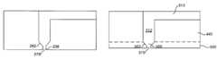
- the nozzle depthis selected by forming the nozzle feature in a layer of material having the thickness equal to that of the final nozzle depth, and the nozzle 224 is formed to have a cross-section with substantially consistent geometry, such as perpendicular walls 230 , as shown in FIG. 2A .
- multiple etching techniquesare employed to form a nozzle having multiple portions that each have a different geometry.
- the nozzle 224is formed to have an upper portion that has a conical or pyramidal cross-section 262 and a lower portion with substantially perpendicular walls 236 that leads to the nozzle outlet 275 , as shown in FIG. 2B .
- a multi-layer substratesuch as a silicon-on-insulator (SOI) substrate 400
- SOI substrate 400can be formed or provided.
- the SOI substrate 400includes a handle layer of silicon 416 , an insulator layer 410 and a nozzle layer of silicon 420 .
- One method of forming an SOI substrateis to grow an oxide layer on a double side polished (DSP) silicon substrate to form the insulator layer 410 .
- the oxide layercan be from 0.1 to 100 microns thick, such as about 5 microns.
- a second double side polished silicon substratecan then be bonded to the exposed surface of the oxide layer to complete the SOI substrate 400 .
- the oxidecan be grown on all exposed surfaces of the substrate. After the bonding step, any exposed oxide that is not desired can be etched away, such as by dry etching.
- the SOI substrate 400can include an insulator layer 410 of silicon nitride instead of an oxide.
- a silicon layercan be formed on the insulator layer 410 , such as by a deposition process.
- the nozzle layer 420 of the SOI substrate 400is thinned to a desired thickness 402 .
- One or more grinding and/or etching stepscan be used to achieve the desired nozzle layer thickness 402 .
- the nozzle layer 420is ground as much as possible to achieve the desired thickness, because grinding can control thickness precisely.
- the nozzle layer thickness 402can be about 10 to 100 microns, e.g., between about 40 and 60 microns.
- a final polish of the back side 426 of the nozzle layer 420can decrease surface roughness. Surface roughness is a factor in achieving a silicon to silicon bond, as described below.
- the polishing stepcan introduce uncertainty in thickness and is not used for achieving the desired thickness.
- the back side 426 of the nozzle layer 420is prepared for processing.
- the processingcan include etching.
- One exemplary etching processis described, however, other methods may be suitable for etching the nozzle layer 420 .
- the SOI substrate 400can be oxidized to form a back side oxide layer 432 and a front side oxide layer 438 .
- a resist layer 436is then coated on the back side oxide layer 432 .
- the resist 436is patterned to define the location 441 of the nozzle. Patterning the resist 436 can include conventional photolithographic techniques followed by developing or washing the resist 436 .
- the nozzlecan have a cross section that is substantially free of corners, such as a circular, elliptical or racetrack shape.
- the back side oxide layer 432is then etched, as shown in FIG. 6 .
- the resist layer 436can optionally be removed after the oxide etch.
- the silicon nozzle layer 420is then etched to form the nozzle 460 , as shown in FIG. 7A .
- the insulator layer 410serves as an etch stop.
- the silicon nozzle layer 420can be etched, for example, by deep reactive ion etching (DRIE).
- DRIEutilizes plasma to selectively etch silicon to form features with substantially vertical sidewalls.
- DRIEis substantially insensitive to silicon geometry and etches a straight walled hole to within ⁇ 1°.
- a reactive ion etching technique known as the Bosch processis discussed in Laermor et al. U.S. Pat. No. 5,501,893, the entire contents of which is incorporated hereby by reference.
- the Bosch techniquecombines an etching step with a polymer deposition to etch relatively deep features. Because of the alternative etching and deposition, the walls can have a slight scallop contour, which can keep the walls from being perfectly flat.
- Other suitable DRIE etch techniquescan alternatively be used to etch the nozzle layer 420 .
- Deep silicon reactive ion etching equipmentis available from Surface Technology Systems, Ltd., located in Redwood City, Calif., Alcatel, located in Plano, Tex., or Unaxis, located in Switzerland and reactive ion etching can be conducted by etching vendors including Innovative Micro Technology, located in Santa Barbara, Calif. DRIE is used due to its ability to cut deep features of substantially constant diameter. Etching is performed in a vacuum chamber with plasma and gas, such as, SF 6 and C 4 F 8 .
- an etchis performed to create tapered walls, as shown in FIG. 7B .
- Tapered wallscan be formed by anisotropically etching the silicon substrate.
- An anisotropic etchsuch as a wet etch technique, can include, but is not limited to, a technique that uses ethylenediamene or KOH as the etchant.
- Anisotropic etchingremoves molecules from the 100 plane much more quickly than from the 111 plane, thus forming the tapered walls.
- An anisotropic etch on a substrate with the 111 plane at the exposed surfaceexhibits a different etch geometry than a substrate with a 100 plane at the surface.
- the back side oxide layer 432is stripped from the substrate, such as, by etching, as shown in FIG. 8 .
- the etched silicon nozzle layer 420is then aligned to a flow path module 440 that has the descender 512 and other flow path features, such as a pumping chamber 513 , in preparation for bonding, as shown in FIG. 9 .
- the surfaces of the flow path module 440 and the nozzle layer 420are first cleaned, such as by reverse RCA cleaning, i.e., performing an RCA2 clean consisting of a mixture of DI water, hydrochloric acid and hydrogen peroxide followed by an RCA1 clean in a bath of DI water, ammonium hydroxide and hydrogen peroxide.
- the cleaningprepares the two elements for direct silicon bonding, or the creation of Van der Waal's bonds between the two silicon surfaces.
- Direct silicon bondingcan occur when two flat, highly polished, clean silicon surfaces are brought together with no intermediate layer between the two silicon layers.
- the flow path module 440 and the nozzle layer 420are positioned so that the descender 512 is aligned with the nozzle 460 .
- the flow path module 440 and nozzle layer 420are then brought together. Pressure is placed at a central point of the two layers and allowed to work its way toward the edges. This method reduces the likelihood of voids forming at the interface of the two layers.
- the layersare annealed at an annealing temperature, for example, around 1050° C.-1100° C.
- An advantage of direct silicon bondingis that no additional layer is formed between the flow path module 440 and the nozzle layer 420 .
- the two silicon layersbecome one unitary layer such that no or virtually no delineation between the two layers exists when the bonding is complete, as shown in FIG. 10 (the dotted line shows the former surfaces of the flow path module 440 and nozzle layer 420 ).
- a silicon layer and an oxide layercan be anodically bonded together.
- the anodic bondingincludes bringing together the silicon and oxide layers and applying a voltage across the substrates to induce a chemical bond.
- the handle layer 416is removed. Specifically, the handle layer 416 can be subjected to a bulk polishing process (and optionally a finer grinding or etching process) to remove a portion of the thickness, as shown in FIG. 11 .
- the oxide layercan be completely removed by etching, thus exposing the nozzle opening.
- this implementationhas parallel side walls, the nozzle could have tapered walls if the etching process shown in FIG. 7B were to be used.
- the insulator layer 410can be left on the nozzle layer 420 and etched through from the outer surface to form a part of the nozzle opening.
- the back side etch processis performed to create a nozzle with multiple portions having different geometries.
- the nozzlecan be formed in either a 100 plane DSP wafer or a SOI substrate with a nozzle layer 500 that is a 100 plane silicon, as shown in FIG. 14 .
- the nozzle layer 500can be thinned to the desired thickness, as described above.
- the thicknesscan be between around 1 and 100 microns, such as between about 20 and 80 microns, e.g., around 30 to 70 microns.
- an oxide layeris grown on the silicon nozzle layer 500 to form a back side oxide 526 .
- An insulator layer 538 and a handle layer 540are on the opposite side of the nozzle layer 500 from the back side oxide 526 .
- a resistcan be formed on the back side oxide 526 , such as by spinning-on the resist.
- the resistcan be patterned to define the location of the nozzle. The location of the nozzle is formed by creating an opening 565 in the back side oxide 526 .
- the nozzle layer 500is etched using an anisotropic etch, such as a wet etch technique.
- the etchdefines a recess 566 in the silicon nozzle layer 500 that has an inverted pyramid shape, or is the shape of a pyramidal frustum with a base, a recessed surface 557 parallel to the base and sloped walls 562 .
- the tapered wall 562meets the recessed surface 557 at an edge having a length 560 .
- the recess 566can be etched through to the insulator layer 538 , as shown in FIG. 16A .
- the recess 566can extend only partially through the nozzle layer 500 , as shown in FIG. 16B .
- substantially constant recess depthscan be achieved by controlling the etch time and rate.
- a wet etch using KOHhas an etch rate that is dependent on temperature.
- the recess 566can be about 1 to about 100 microns deep, such as about 3 to 50 microns.
- the etched nozzle layer 500is joined with a flow path module 440 .
- the nozzle layer 500is joined with the flow path module 440 so that the descender 512 is aligned with the recess 566 .
- the nozzle layer 500 and the flow path module 440can be bonded together with an adhesive, an anodic bond or a direct silicon bond (fusion bond). If a direct silicon bond is selected, the back side oxide 526 is removed prior to bonding.
- the handle layer 540is removed.
- the handle layer 540can be removed, such as by grinding, etching or a combination of grinding and etching.
- the front side of the nozzle layer 500is also etched. As shown in FIG. 19 , the front side is prepared for etching by coating a resist 546 on the insulator layer 538 and patterning the resist 546 , as described above. The resist is patterned such that the underlying insulator layer 538 is exposed in areas that correspond to the recesses 566 formed in the back side of the nozzle layer 500 .
- a view of the front side of the nozzle layer 500shows that the resist 546 can be patterned with a circular opening 571 or a rectangular opening 572 .
- Other opening geometriesmay be suitable, such as a polygon with five or more sides.
- the exposed oxideis etched in a location 559 corresponding to the recess 566 to expose the underlying nozzle layer 500 , as shown in FIG. 21 .
- the nozzle layer 500is etched to form a nozzle outlet 575 .
- the etch process usedcan be DRIE, so that the nozzle outlet 575 has substantially straight walls, as described above. This can form a nozzle outlet 575 that converges at a point beyond the exterior of the nozzle outlet 575 .
- the nozzle outletcan be about 5 to 40 microns in diameter, such as about 25 microns in diameter.
- the diameter 577 of the nozzle outlet 575is sufficient to intersect the tapered walls 562 of the recess 566 .
- the nozzle recess 566forms the nozzle entry.
- a side cross sectional view of the nozzle layershows the intersection of the tapered walls 562 and the nozzle outlet 575 .
- the diameter of the nozzle outlet 575is large enough so that the intersection between the recess 566 and the nozzle outlet 575 can remove any portion of the recessed surface 557 , even if the recess 566 did not extend to the insulator layer when the recess was formed. Therefore, the nozzle outlet 575 is formed to have a dimension 577 that is equal to or greater than the length 560 of the wall 562 where the wall 562 meets the recessed surface 557 . In one implementation, the diameter of the nozzle outlet 575 is less than the recessed surface of the pyramidal frustum and a portion of the recessed surface remains after the outlet 575 is formed.
- the nozzle layer processingis completed.
- the back side oxide layer 526is removed.
- the pyramidal nozzle inletcan have a depth of between about 10 to 100 microns, such as about 30 microns.
- the nozzle outlet 575can have a depth of between about 2 and about 20 microns, such as about 5 microns.
- Modificationscan be made to the above mentioned processes to achieved the desired nozzle geometry.
- all of the etchingis performed from the back side of the nozzle layer 500 .
- the insulator layer 538is not removed from the nozzle.
- the insulator layer 538can be etched so that the walls of the opening are substantially the same as the walls of the nozzle outlet 575 , as shown in FIG. 22 .
- the walls of the opening in the insulator layer 538can be different from the walls of the nozzle outlet 575 .
- the nozzle opening 575can have tapered walls that lead into a straight walled portion formed in the insulator layer 538 . Forming the opening in the insulator layer 538 can either occur before or after attaching the nozzle layer 500 with a flow path module 440 .
- the depth of the nozzlesmay be limited to a particular range of thicknesses, such as more than about 200 microns. Processing substrates thinner than about 200 microns can lead to a drop in yield, because of the increased likelihood of damaging or breaking the substrate.
- a substrategenerally should be thick enough to facilitate substrate handling during processing. If the nozzles are formed in a layer of an SOI substrate, the layer can be ground to the desired thickness prior to formation while still providing a different thickness for handling.
- the handle layeralso provides a portion that can be grasped during processing without interfering with the processing of the nozzle layer.
- Forming the nozzle in a layer of a desired thicknesscan obviate the step of reducing the nozzle layer after the nozzle layer has been joined with the flow path module. Grinding away the handle layer after the nozzle layer is joined with the flow path module does not leave the flow path features open to grinding solution or waste grinding material.
- the insulator layercan be selectively removed so that the underlying silicon layer is not etched.
- a nozzle formation processthat uses two types of processing can form nozzles with intricate geometries.
- An anisotropic back side etchcan form a recess in the shape of a pyramidal frustum having a base at the surface of the substrate, sloped or tapered walls and a recessed surface in the substrate.
- a front side etchthat is configured so that the diameter is greater than the diameter of the recessed surface of the pyramidal frustum removes the recessed surface of the pyramidal frustum shape from the recess and the nozzle. This technique removes any substantially flat surface that is orthogonal to the direction of ink flow from the nozzle. This can reduce the incident of trapped air in the nozzle.
- tapered walls that are formed by the anisotropic etchcan keep the ink flow resistance low, while accommodating a large amount of meniscus pull-back during fill without air ingestion.
- the tapered walls of the nozzlesmoothly transitions into the straight parallel walls of the nozzle opening, minimizing the tendency of the flow to separate from the walls.
- the straight parallel walls of the nozzle openingcan direct the stream or droplet of ink out of the nozzle.
- the depth of the anisotropic etchdirectly affects the length of both the nozzle entry and the nozzle outlet if the nozzle opening is not formed with a diameter greater than the diameter of the recessed surface of the pyramidal frustum.
- the anisotropic etch depthis determined by the length of time of the etch along with the temperature at which the etch is performed and can be difficult to control.
- the geometry of a DRIE etchmay be easier to control than the depth of an anisotropic etch.
Landscapes
- Engineering & Computer Science (AREA)
- Manufacturing & Machinery (AREA)
- Particle Formation And Scattering Control In Inkjet Printers (AREA)
Abstract
Description
Claims (17)
Priority Applications (12)
| Application Number | Priority Date | Filing Date | Title |
|---|---|---|---|
| US10/913,571US7347532B2 (en) | 2004-08-05 | 2004-08-05 | Print head nozzle formation |
| CNA2005800337654ACN101035682A (en) | 2004-08-05 | 2005-08-04 | print head nozzle formation |
| PCT/US2005/028064WO2006017808A2 (en) | 2004-08-05 | 2005-08-04 | Print head nozzle formation |
| JP2007525061AJP4874246B2 (en) | 2004-08-05 | 2005-08-04 | Nozzle formation of print head |
| KR1020077003756AKR101273436B1 (en) | 2004-08-05 | 2005-08-04 | Print head nozzle formation |
| CN201510556516.9ACN105109207A (en) | 2004-08-05 | 2005-08-04 | Print head nozzle formation |
| HK07112674.1AHK1104263B (en) | 2004-08-05 | 2005-08-04 | Print head nozzle formation |
| EP05783403AEP1786628B1 (en) | 2004-08-05 | 2005-08-04 | Print head nozzle formation |
| CN201110436821.6ACN102582262B (en) | 2004-08-05 | 2005-08-04 | Print-head nozzle is formed |
| US12/027,597US8377319B2 (en) | 2004-08-05 | 2008-02-07 | Print head nozzle formation |
| JP2011089638AJP5118227B2 (en) | 2004-08-05 | 2011-04-13 | Nozzle formation of print head |
| HK16106303.1AHK1218278A1 (en) | 2004-08-05 | 2016-06-02 | Print head nozzle formation |
Applications Claiming Priority (1)
| Application Number | Priority Date | Filing Date | Title |
|---|---|---|---|
| US10/913,571US7347532B2 (en) | 2004-08-05 | 2004-08-05 | Print head nozzle formation |
Related Child Applications (1)
| Application Number | Title | Priority Date | Filing Date |
|---|---|---|---|
| US12/027,597DivisionUS8377319B2 (en) | 2004-08-05 | 2008-02-07 | Print head nozzle formation |
Publications (2)
| Publication Number | Publication Date |
|---|---|
| US20060028508A1 US20060028508A1 (en) | 2006-02-09 |
| US7347532B2true US7347532B2 (en) | 2008-03-25 |
Family
ID=35159850
Family Applications (2)
| Application Number | Title | Priority Date | Filing Date |
|---|---|---|---|
| US10/913,571Expired - LifetimeUS7347532B2 (en) | 2004-08-05 | 2004-08-05 | Print head nozzle formation |
| US12/027,597Active2027-04-24US8377319B2 (en) | 2004-08-05 | 2008-02-07 | Print head nozzle formation |
Family Applications After (1)
| Application Number | Title | Priority Date | Filing Date |
|---|---|---|---|
| US12/027,597Active2027-04-24US8377319B2 (en) | 2004-08-05 | 2008-02-07 | Print head nozzle formation |
Country Status (7)
| Country | Link |
|---|---|
| US (2) | US7347532B2 (en) |
| EP (1) | EP1786628B1 (en) |
| JP (2) | JP4874246B2 (en) |
| KR (1) | KR101273436B1 (en) |
| CN (3) | CN101035682A (en) |
| HK (1) | HK1218278A1 (en) |
| WO (1) | WO2006017808A2 (en) |
Cited By (14)
| Publication number | Priority date | Publication date | Assignee | Title |
|---|---|---|---|---|
| US20070030306A1 (en)* | 2005-07-01 | 2007-02-08 | Yoshimasa Okamura | Non-wetting coating on a fluid ejector |
| US20080136866A1 (en)* | 2006-12-01 | 2008-06-12 | Fujifilm Dimatix, Inc. | Non-wetting coating on a fluid ejector |
| US20090085976A1 (en)* | 1997-07-15 | 2009-04-02 | Silverbrook Research Pty Ltd | Nozzle arrangement for an inkjet printhead having an ink ejecting roof structure |
| US20090267991A1 (en)* | 1997-07-15 | 2009-10-29 | Silverbrook Research Pty Ltd | Printhead module for wide format pagewidth inkjet printer |
| US20100053268A1 (en)* | 1998-10-16 | 2010-03-04 | Silverbrook Research Pty Ltd | Nozzle Arrangement With Laminated Ink Ejection Member And Ink Spread Prevention Rim |
| US20100110144A1 (en)* | 2008-10-31 | 2010-05-06 | Andreas Bibl | Applying a Layer to a Nozzle Outlet |
| US20100141709A1 (en)* | 2008-10-31 | 2010-06-10 | Gregory Debrabander | Shaping a Nozzle Outlet |
| US20100165048A1 (en)* | 2008-12-30 | 2010-07-01 | Gregory Debrabander | Forming nozzles |
| US20100220148A1 (en)* | 2009-02-27 | 2010-09-02 | Christoph Menzel | Nozzle Shape For Fluid Droplet Ejection |
| US20110063369A1 (en)* | 2009-09-15 | 2011-03-17 | Fujifilm Corporation | Non-Wetting Coating on a Fluid Ejector |
| US20110181664A1 (en)* | 2010-01-27 | 2011-07-28 | Fujifilm Corporation | Forming Self-Aligned Nozzles |
| US20110205306A1 (en)* | 2010-02-25 | 2011-08-25 | Vaeth Kathleen M | Reinforced membrane filter for printhead |
| US8733897B2 (en) | 2008-10-30 | 2014-05-27 | Fujifilm Corporation | Non-wetting coating on a fluid ejector |
| US8960848B2 (en) | 2011-09-21 | 2015-02-24 | Fujifilm Corporation | Liquid ejection head, liquid ejection apparatus and abnormality detection method for liquid ejection head |
Families Citing this family (30)
| Publication number | Priority date | Publication date | Assignee | Title |
|---|---|---|---|---|
| US7444197B2 (en) | 2004-05-06 | 2008-10-28 | Smp Logic Systems Llc | Methods, systems, and software program for validation and monitoring of pharmaceutical manufacturing processes |
| US7799273B2 (en) | 2004-05-06 | 2010-09-21 | Smp Logic Systems Llc | Manufacturing execution system for validation, quality and risk assessment and monitoring of pharmaceutical manufacturing processes |
| US7347532B2 (en)* | 2004-08-05 | 2008-03-25 | Fujifilm Dimatix, Inc. | Print head nozzle formation |
| JP2008094018A (en)* | 2006-10-13 | 2008-04-24 | Seiko Epson Corp | Nozzle plate manufacturing method and droplet discharge head manufacturing method |
| JP4881126B2 (en)* | 2006-10-25 | 2012-02-22 | 株式会社東芝 | Nozzle plate manufacturing method and droplet discharge head manufacturing method |
| WO2008077419A1 (en)* | 2006-12-22 | 2008-07-03 | Telecom Italia S.P.A. | Ink-jet printhead manufacturing process |
| WO2008124107A1 (en)* | 2007-04-04 | 2008-10-16 | The Regents Of The University Of California | Compositions, devices, systems, and methods for using a nanopore |
| KR101126169B1 (en)* | 2007-05-17 | 2012-03-23 | 삼성전자주식회사 | MEMS device and Method for manufacturing the same |
| JP2009083140A (en)* | 2007-09-27 | 2009-04-23 | Fujifilm Corp | Liquid discharge head and manufacturing method thereof |
| JP5207544B2 (en)* | 2009-02-24 | 2013-06-12 | 富士フイルム株式会社 | Inkjet head manufacturing method and inkjet recording apparatus |
| KR20110000960A (en)* | 2009-06-29 | 2011-01-06 | 삼성전자주식회사 | Semiconductor chip, stack module, memory card and manufacturing method thereof |
| JP5723109B2 (en)* | 2010-06-14 | 2015-05-27 | 富士フイルム株式会社 | Method for manufacturing liquid discharge head |
| KR101890755B1 (en) | 2011-11-25 | 2018-08-23 | 삼성전자 주식회사 | Inkjet printing device and nozzle forming method |
| JP5725664B2 (en)* | 2012-03-14 | 2015-05-27 | 富士フイルム株式会社 | Nozzle plate manufacturing method |
| JP5645863B2 (en)* | 2012-03-14 | 2014-12-24 | 富士フイルム株式会社 | Nozzle plate manufacturing method |
| US8790195B1 (en)* | 2012-12-27 | 2014-07-29 | Callaway Golf Company | Golf club head with adjustable characteristics |
| JP5943755B2 (en)* | 2012-07-20 | 2016-07-05 | キヤノン株式会社 | Method for manufacturing substrate of liquid discharge head |
| KR101941168B1 (en) | 2012-10-09 | 2019-01-22 | 삼성전자주식회사 | Inkjet rinting device |
| WO2015011608A1 (en) | 2013-07-22 | 2015-01-29 | Koninklijke Philips N.V. | A mesh for use in a nebuliser, and a method of manufacturing the same |
| JP2015036202A (en)* | 2013-08-12 | 2015-02-23 | 富士フイルム株式会社 | Inkjet head manufacturing method |
| CN107405922B (en)* | 2015-03-24 | 2020-06-30 | 锡克拜控股有限公司 | Manufacturing method of ink jet print head |
| US10198047B2 (en) | 2015-11-19 | 2019-02-05 | Dell Products, Lp | Data storage device connector with integrated temperature sensor |
| JP6883042B2 (en)* | 2015-12-31 | 2021-06-02 | フジフィルム ディマティックス, インコーポレイテッド | Liquid discharge device |
| US10138546B2 (en)* | 2016-08-10 | 2018-11-27 | Corning Incorporated | Apparatus and method to coat glass substrates with electrostatic chuck and van der waals forces |
| CN106553453A (en)* | 2016-12-06 | 2017-04-05 | 苏州工业园区纳米产业技术研究院有限公司 | Hot bubble type ink jet printhead and preparation method thereof |
| US10052875B1 (en)* | 2017-02-23 | 2018-08-21 | Fujifilm Dimatix, Inc. | Reducing size variations in funnel nozzles |
| CN107187205B (en)* | 2017-06-08 | 2019-09-24 | 翁焕榕 | Nozzle plate and preparation method thereof and ink-jet printer |
| JPWO2020066333A1 (en)* | 2018-09-27 | 2021-04-30 | 富士フイルム株式会社 | Ink tank, inkjet recording device, and inkjet recording method |
| JP7384561B2 (en)* | 2019-02-18 | 2023-11-21 | ローム株式会社 | Nozzle substrate, inkjet print head and nozzle substrate manufacturing method |
| CN114368222A (en)* | 2022-01-21 | 2022-04-19 | 武汉敏捷微电子有限公司 | Microfluid device and manufacturing method thereof |
Citations (16)
| Publication number | Priority date | Publication date | Assignee | Title |
|---|---|---|---|---|
| US3921916A (en) | 1974-12-31 | 1975-11-25 | Ibm | Nozzles formed in monocrystalline silicon |
| US4007464A (en) | 1975-01-23 | 1977-02-08 | International Business Machines Corporation | Ink jet nozzle |
| US4475113A (en) | 1981-06-18 | 1984-10-02 | International Business Machines | Drop-on-demand method and apparatus using converging nozzles and high viscosity fluids |
| EP0576007A2 (en) | 1992-06-24 | 1993-12-29 | Seiko Epson Corporation | Method of forming a nozzle for an ink-jet printer head |
| US5640184A (en) | 1994-03-21 | 1997-06-17 | Spectra, Inc. | Orifice plate for simplified ink jet head |
| US5992974A (en)* | 1995-07-03 | 1999-11-30 | Seiko Epson Corporation | Ink-jet head having nozzle openings with a constant width and manufacturing method thereof |
| EP0985534A1 (en) | 1997-05-14 | 2000-03-15 | Seiko Epson Corporation | Method of forming nozzle for injectors and method of manufacturing ink jet head |
| US6170934B1 (en) | 1997-02-18 | 2001-01-09 | Fujitsu Limited | Method for apparatus for producing a nozzle plate of an ink-jet head printer |
| US6213587B1 (en)* | 1999-07-19 | 2001-04-10 | Lexmark International, Inc. | Ink jet printhead having improved reliability |
| US6238584B1 (en) | 1999-03-02 | 2001-05-29 | Eastman Kodak Company | Method of forming ink jet nozzle plates |
| US6375313B1 (en) | 2001-01-08 | 2002-04-23 | Hewlett-Packard Company | Orifice plate for inkjet printhead |
| US6423476B1 (en) | 1999-12-22 | 2002-07-23 | Samsung Electronics Co., Ltd. | Method of manufacturing a nozzle plate |
| US20030112300A1 (en) | 2001-12-18 | 2003-06-19 | Jae-Woo Chung | Piezoelectric ink-jet printhead and method for manufacturing the same |
| EP1332879A1 (en) | 2002-01-31 | 2003-08-06 | Scitex Digital Printing, Inc. | Mandrel with controlled release layer for multi-layer electroformed ink jet orifice plates |
| US6718632B2 (en) | 2001-01-29 | 2004-04-13 | Hewlett-Packard Development Company, L.P. | Method of making a fluid-jet ejection device |
| US20040085409A1 (en) | 1996-01-26 | 2004-05-06 | Seiko Epson Corporation | Ink jet recording head having piezoelectric element and electrode patterned with same shape and without pattern shift therebetween |
Family Cites Families (30)
| Publication number | Priority date | Publication date | Assignee | Title |
|---|---|---|---|---|
| US4412001A (en)* | 1981-01-30 | 1983-10-25 | Board Of Trustees Of The University Of Illinois | Isolation of bacterial luciferase |
| DE3369807D1 (en)* | 1982-07-05 | 1987-03-19 | Siemens Ag | Method and device for automatically demanding signal measure values and/or signal identification in an alarm installation |
| DE3327610A1 (en)* | 1983-07-30 | 1985-02-07 | Franz Bendig | DEVICE FOR CONTROLLING THE MOVEMENT PROCESS IN A FILM PROCESSING MACHINE |
| JPS6192865A (en)* | 1984-10-12 | 1986-05-10 | Pioneer Electronic Corp | Method for processing crystalline substrate |
| DE4241045C1 (en) | 1992-12-05 | 1994-05-26 | Bosch Gmbh Robert | Process for anisotropic etching of silicon |
| US5562801A (en)* | 1994-04-28 | 1996-10-08 | Cypress Semiconductor Corporation | Method of etching an oxide layer |
| DE69534271T2 (en)* | 1994-07-11 | 2006-05-11 | Kabushiki Kaisha Toshiba, Kawasaki | Ink jet recording apparatus |
| US6729002B1 (en)* | 1995-09-05 | 2004-05-04 | Seiko Epson Corporation | Method of producing an ink jet recording head |
| JPH09267479A (en)* | 1996-03-29 | 1997-10-14 | Seiko Epson Corp | Inkjet head manufacturing method |
| JPH10315461A (en)* | 1997-05-14 | 1998-12-02 | Seiko Epson Corp | Ink jet head and method of manufacturing the same |
| EP1005986B1 (en) | 1998-06-18 | 2006-08-23 | Matsushita Electric Industrial Co., Ltd. | Fluid jetting device and its production process |
| KR100325520B1 (en)* | 1998-12-10 | 2002-04-17 | 윤종용 | Manufacturing Method of Fluid Injection Device_ |
| US6483812B1 (en)* | 1999-01-06 | 2002-11-19 | International Business Machines Corporation | Token ring network topology discovery and display |
| JP2001071512A (en) | 1999-02-10 | 2001-03-21 | Canon Inc | Method for manufacturing liquid discharge head, liquid discharge head, and method for manufacturing discharge port plate |
| JP2000269106A (en) | 1999-03-16 | 2000-09-29 | Nippon Dempa Kogyo Co Ltd | Substrate direct bonding method |
| US6378995B1 (en)* | 1999-07-07 | 2002-04-30 | Samsung Electronics Co., Ltd. | Manufacturing method of nozzle plate using silicon process and ink jet printer head applying the nozzle plate |
| US6180533B1 (en)* | 1999-08-10 | 2001-01-30 | Applied Materials, Inc. | Method for etching a trench having rounded top corners in a silicon substrate |
| DE69942507D1 (en)* | 1999-12-06 | 2010-07-29 | Ericsson Telefon Ab L M | Intelligent production of piconets |
| TW514596B (en)* | 2000-02-28 | 2002-12-21 | Hewlett Packard Co | Glass-fiber thermal inkjet print head |
| US6990080B2 (en)* | 2000-08-07 | 2006-01-24 | Microsoft Corporation | Distributed topology control for wireless multi-hop sensor networks |
| JP2002127429A (en)* | 2000-10-20 | 2002-05-08 | Konica Corp | Method for manufacturing ink jet recording head and ink jet recording head |
| JP3743883B2 (en)* | 2000-11-28 | 2006-02-08 | カシオ計算機株式会社 | Inkjet printer head forming method |
| JP3800317B2 (en) | 2001-01-10 | 2006-07-26 | セイコーエプソン株式会社 | Inkjet recording head and inkjet recording apparatus |
| US20020140774A1 (en)* | 2001-03-30 | 2002-10-03 | Olympus Optical Co., Ltd. | Ink head |
| JP2003094667A (en) | 2001-09-21 | 2003-04-03 | Ricoh Co Ltd | Method of manufacturing droplet discharge head |
| US6679587B2 (en)* | 2001-10-31 | 2004-01-20 | Hewlett-Packard Development Company, L.P. | Fluid ejection device with a composite substrate |
| JP3856119B2 (en)* | 2002-02-15 | 2006-12-13 | セイコーエプソン株式会社 | Nozzle plate, manufacturing method thereof, and ink jet recording head |
| US7122903B2 (en)* | 2003-10-21 | 2006-10-17 | Sharp Kabushiki Kaisha | Contact plug processing and a contact plug |
| US7347532B2 (en)* | 2004-08-05 | 2008-03-25 | Fujifilm Dimatix, Inc. | Print head nozzle formation |
| JP4706850B2 (en)* | 2006-03-23 | 2011-06-22 | 富士フイルム株式会社 | Nozzle plate manufacturing method, droplet discharge head, and image forming apparatus |
- 2004
- 2004-08-05USUS10/913,571patent/US7347532B2/ennot_activeExpired - Lifetime
- 2005
- 2005-08-04WOPCT/US2005/028064patent/WO2006017808A2/enactiveApplication Filing
- 2005-08-04CNCNA2005800337654Apatent/CN101035682A/enactivePending
- 2005-08-04JPJP2007525061Apatent/JP4874246B2/ennot_activeExpired - Lifetime
- 2005-08-04KRKR1020077003756Apatent/KR101273436B1/ennot_activeExpired - Fee Related
- 2005-08-04CNCN201110436821.6Apatent/CN102582262B/ennot_activeExpired - Lifetime
- 2005-08-04CNCN201510556516.9Apatent/CN105109207A/enactivePending
- 2005-08-04EPEP05783403Apatent/EP1786628B1/ennot_activeExpired - Lifetime
- 2008
- 2008-02-07USUS12/027,597patent/US8377319B2/enactiveActive
- 2011
- 2011-04-13JPJP2011089638Apatent/JP5118227B2/ennot_activeExpired - Lifetime
- 2016
- 2016-06-02HKHK16106303.1Apatent/HK1218278A1/enunknown
Patent Citations (20)
| Publication number | Priority date | Publication date | Assignee | Title |
|---|---|---|---|---|
| US3921916A (en) | 1974-12-31 | 1975-11-25 | Ibm | Nozzles formed in monocrystalline silicon |
| US4007464A (en) | 1975-01-23 | 1977-02-08 | International Business Machines Corporation | Ink jet nozzle |
| US4475113A (en) | 1981-06-18 | 1984-10-02 | International Business Machines | Drop-on-demand method and apparatus using converging nozzles and high viscosity fluids |
| EP0576007A2 (en) | 1992-06-24 | 1993-12-29 | Seiko Epson Corporation | Method of forming a nozzle for an ink-jet printer head |
| US5640184A (en) | 1994-03-21 | 1997-06-17 | Spectra, Inc. | Orifice plate for simplified ink jet head |
| US6238585B1 (en) | 1995-07-03 | 2001-05-29 | Seiko Epson Corporation | Method for manufacturing an ink-jet head having nozzle openings with a constant width |
| US5992974A (en)* | 1995-07-03 | 1999-11-30 | Seiko Epson Corporation | Ink-jet head having nozzle openings with a constant width and manufacturing method thereof |
| US20040085409A1 (en) | 1996-01-26 | 2004-05-06 | Seiko Epson Corporation | Ink jet recording head having piezoelectric element and electrode patterned with same shape and without pattern shift therebetween |
| US6170934B1 (en) | 1997-02-18 | 2001-01-09 | Fujitsu Limited | Method for apparatus for producing a nozzle plate of an ink-jet head printer |
| US6375858B1 (en) | 1997-05-14 | 2002-04-23 | Seiko Epson Corporation | Method of forming nozzle for injection device and method of manufacturing inkjet head |
| US6863375B2 (en) | 1997-05-14 | 2005-03-08 | Seiko Epson Corporation | Ejection device and inkjet head with silicon nozzle plate |
| EP0985534A1 (en) | 1997-05-14 | 2000-03-15 | Seiko Epson Corporation | Method of forming nozzle for injectors and method of manufacturing ink jet head |
| US6238584B1 (en) | 1999-03-02 | 2001-05-29 | Eastman Kodak Company | Method of forming ink jet nozzle plates |
| US6213587B1 (en)* | 1999-07-19 | 2001-04-10 | Lexmark International, Inc. | Ink jet printhead having improved reliability |
| US6423476B1 (en) | 1999-12-22 | 2002-07-23 | Samsung Electronics Co., Ltd. | Method of manufacturing a nozzle plate |
| US6375313B1 (en) | 2001-01-08 | 2002-04-23 | Hewlett-Packard Company | Orifice plate for inkjet printhead |
| US6718632B2 (en) | 2001-01-29 | 2004-04-13 | Hewlett-Packard Development Company, L.P. | Method of making a fluid-jet ejection device |
| US20030112300A1 (en) | 2001-12-18 | 2003-06-19 | Jae-Woo Chung | Piezoelectric ink-jet printhead and method for manufacturing the same |
| US7121650B2 (en) | 2001-12-18 | 2006-10-17 | Samsung Electronics Co., Ltd. | Piezoelectric ink-jet printhead |
| EP1332879A1 (en) | 2002-01-31 | 2003-08-06 | Scitex Digital Printing, Inc. | Mandrel with controlled release layer for multi-layer electroformed ink jet orifice plates |
Non-Patent Citations (6)
| Title |
|---|
| Bassous, E. et al., "Ink jet printing nozzle arrays etched in silicon", 1977, Applied Phys. Lett., vol. 31, p. 134-137. |
| Bassous, E. et al., "The Fabrication of high precision nozzles by the anisotropic etching of(100) silicon", 1978, J. Electrochem, Soc., vol. 125, pp. 1321-1327. |
| Bassous, E., "Fabrication of novel three-dimensional microstructures by the anisotropic etching of (100) and (110) silicon", 1978, IEEE Trans. Electron Devices, vol. ED-25, pp. 1178-1185. |
| International Search Report and Written Opinion of the International Searching Authority, International Application Serial No. PCT/US2005/028064, Feb 2, 2006, 13 pp. |
| Partial International Search Report, International Application Serial No. PCT/US2005/028064, Nov. 22, 2005, 4 pp. |
| Petersen, Kurt E. (Member, IEEE), "Silicon as a Mechanical Material", 1982, IEEE, pp. 420-457. |
Cited By (29)
| Publication number | Priority date | Publication date | Assignee | Title |
|---|---|---|---|---|
| US8408679B2 (en) | 1997-07-15 | 2013-04-02 | Zamtec Ltd | Printhead having CMOS drive circuitry |
| US8287105B2 (en)* | 1997-07-15 | 2012-10-16 | Zamtec Limited | Nozzle arrangement for an inkjet printhead having an ink ejecting roof structure |
| US20090085976A1 (en)* | 1997-07-15 | 2009-04-02 | Silverbrook Research Pty Ltd | Nozzle arrangement for an inkjet printhead having an ink ejecting roof structure |
| US20090267991A1 (en)* | 1997-07-15 | 2009-10-29 | Silverbrook Research Pty Ltd | Printhead module for wide format pagewidth inkjet printer |
| US20090295868A1 (en)* | 1997-07-15 | 2009-12-03 | Silverbrook Research Pty Ltd | Printhead Having Ejection Nozzles Over Wide Printing Zone |
| US20090303286A1 (en)* | 1997-07-15 | 2009-12-10 | Silverbrook Research Pty Ltd | Printhead For Wide Format High Resolution Printing |
| US20100026763A1 (en)* | 1997-07-15 | 2010-02-04 | Silverbrook Research Pty Ltd | Printhead having cmos drive circuitry |
| US8419165B2 (en) | 1997-07-15 | 2013-04-16 | Zamtec Ltd | Printhead module for wide format pagewidth inkjet printer |
| US20100053268A1 (en)* | 1998-10-16 | 2010-03-04 | Silverbrook Research Pty Ltd | Nozzle Arrangement With Laminated Ink Ejection Member And Ink Spread Prevention Rim |
| US20110212261A1 (en)* | 2005-07-01 | 2011-09-01 | Yoshimasa Okamura | Non-wetting coating on a fluid ejector |
| US8523322B2 (en) | 2005-07-01 | 2013-09-03 | Fujifilm Dimatix, Inc. | Non-wetting coating on a fluid ejector |
| US8226208B2 (en) | 2005-07-01 | 2012-07-24 | Fujifilm Dimatix, Inc. | Non-wetting coating on a fluid ejector |
| US20070030306A1 (en)* | 2005-07-01 | 2007-02-08 | Yoshimasa Okamura | Non-wetting coating on a fluid ejector |
| US8128201B2 (en) | 2006-12-01 | 2012-03-06 | Fujifilm Dimatix, Inc. | Non-wetting coating on a fluid ejector |
| US20080136866A1 (en)* | 2006-12-01 | 2008-06-12 | Fujifilm Dimatix, Inc. | Non-wetting coating on a fluid ejector |
| US9056472B2 (en) | 2008-10-30 | 2015-06-16 | Fujifilm Corporation | Non-wetting coating on a fluid ejector |
| US8733897B2 (en) | 2008-10-30 | 2014-05-27 | Fujifilm Corporation | Non-wetting coating on a fluid ejector |
| US20100141709A1 (en)* | 2008-10-31 | 2010-06-10 | Gregory Debrabander | Shaping a Nozzle Outlet |
| US20100110144A1 (en)* | 2008-10-31 | 2010-05-06 | Andreas Bibl | Applying a Layer to a Nozzle Outlet |
| US20100165048A1 (en)* | 2008-12-30 | 2010-07-01 | Gregory Debrabander | Forming nozzles |
| US8641171B2 (en) | 2008-12-30 | 2014-02-04 | Fujifilm Corporation | Forming nozzles |
| US8197029B2 (en) | 2008-12-30 | 2012-06-12 | Fujifilm Corporation | Forming nozzles |
| US8303082B2 (en) | 2009-02-27 | 2012-11-06 | Fujifilm Corporation | Nozzle shape for fluid droplet ejection |
| US20100220148A1 (en)* | 2009-02-27 | 2010-09-02 | Christoph Menzel | Nozzle Shape For Fluid Droplet Ejection |
| US8262200B2 (en) | 2009-09-15 | 2012-09-11 | Fujifilm Corporation | Non-wetting coating on a fluid ejector |
| US20110063369A1 (en)* | 2009-09-15 | 2011-03-17 | Fujifilm Corporation | Non-Wetting Coating on a Fluid Ejector |
| US20110181664A1 (en)* | 2010-01-27 | 2011-07-28 | Fujifilm Corporation | Forming Self-Aligned Nozzles |
| US20110205306A1 (en)* | 2010-02-25 | 2011-08-25 | Vaeth Kathleen M | Reinforced membrane filter for printhead |
| US8960848B2 (en) | 2011-09-21 | 2015-02-24 | Fujifilm Corporation | Liquid ejection head, liquid ejection apparatus and abnormality detection method for liquid ejection head |
Also Published As
| Publication number | Publication date |
|---|---|
| WO2006017808A3 (en) | 2006-04-20 |
| JP2008509024A (en) | 2008-03-27 |
| CN102582262A (en) | 2012-07-18 |
| KR20070040395A (en) | 2007-04-16 |
| EP1786628B1 (en) | 2012-10-03 |
| CN105109207A (en) | 2015-12-02 |
| JP4874246B2 (en) | 2012-02-15 |
| KR101273436B1 (en) | 2013-06-11 |
| US8377319B2 (en) | 2013-02-19 |
| HK1218278A1 (en) | 2017-02-10 |
| CN101035682A (en) | 2007-09-12 |
| JP2011156873A (en) | 2011-08-18 |
| US20080128387A1 (en) | 2008-06-05 |
| CN102582262B (en) | 2015-09-30 |
| US20060028508A1 (en) | 2006-02-09 |
| WO2006017808A2 (en) | 2006-02-16 |
| EP1786628A2 (en) | 2007-05-23 |
| HK1104263A1 (en) | 2008-01-11 |
| JP5118227B2 (en) | 2013-01-16 |
Similar Documents
| Publication | Publication Date | Title |
|---|---|---|
| US7347532B2 (en) | Print head nozzle formation | |
| US7622048B2 (en) | Sacrificial substrate for etching | |
| US6557967B1 (en) | Method for making ink-jet printer nozzles | |
| US20100141709A1 (en) | Shaping a Nozzle Outlet | |
| JP2004517755A (en) | Improved inkjet printhead and method of manufacturing the same | |
| JP4660683B2 (en) | Nozzle plate manufacturing method and droplet discharge head manufacturing method | |
| JP2020082503A (en) | Nozzle plate manufacturing method and ink jet head manufacturing method | |
| US20100110144A1 (en) | Applying a Layer to a Nozzle Outlet | |
| JP2007261152A (en) | Nozzle substrate manufacturing method, droplet discharge head manufacturing method, and droplet discharge apparatus manufacturing method | |
| WO2016158917A1 (en) | Method for manufacturing liquid ejection head nozzle plate, liquid ejection head nozzle plate, and liquid ejection head | |
| HK1104263B (en) | Print head nozzle formation | |
| JP2007168344A (en) | Nozzle substrate manufacturing method, droplet discharge head manufacturing method, droplet discharge apparatus manufacturing method, and device manufacturing method | |
| JP2008110560A (en) | Nozzle plate for liquid delivery head, and method for manufacturing nozzle plate for liquid delivering head | |
| JP2007320254A (en) | Nozzle plate manufacturing method, nozzle plate, droplet discharge head manufacturing method, droplet discharge head, droplet discharge device manufacturing method, and droplet discharge device | |
| JP2009119773A (en) | Nozzle plate for liquid discharging head and method for manufacturing the same | |
| JP2009012202A (en) | Nozzle plate manufacturing method, nozzle plate, droplet discharge head manufacturing method, droplet discharge head | |
| JP2006326910A (en) | Inkjet recording substrate | |
| JP2007253390A (en) | Nozzle substrate manufacturing method, droplet discharge head manufacturing method, and droplet discharge apparatus manufacturing method | |
| JP2007307730A (en) | Nozzle substrate manufacturing method, droplet discharge head manufacturing method, and droplet discharge apparatus manufacturing method | |
| JP2007168345A (en) | Droplet discharge head manufacturing method, droplet discharge apparatus manufacturing method, and device manufacturing method | |
| JP2009018423A (en) | Nozzle substrate manufacturing method, nozzle substrate, droplet discharge head, and droplet discharge apparatus | |
| JP2008273078A (en) | Nozzle substrate manufacturing method, droplet discharge head manufacturing method, and droplet discharge apparatus manufacturing method | |
| JP2008284825A (en) | Nozzle substrate manufacturing method and droplet discharge head manufacturing method | |
| HK1105943B (en) | Method of etching using a sacrificial substrate |
Legal Events
| Date | Code | Title | Description |
|---|---|---|---|
| AS | Assignment | Owner name:SPECTRA, INC., NEW HAMPSHIRE Free format text:ASSIGNMENT OF ASSIGNORS INTEREST;ASSIGNORS:CHEN, ZHENFANG;BIBL, ANDREAS;HOISINGTON, PAUL A.;REEL/FRAME:015677/0696 Effective date:20040803 | |
| AS | Assignment | Owner name:DIMATIX, INC.,NEW HAMPSHIRE Free format text:CHANGE OF NAME;ASSIGNOR:SPECTRA, INC.;REEL/FRAME:016361/0929 Effective date:20050502 Owner name:DIMATIX, INC., NEW HAMPSHIRE Free format text:CHANGE OF NAME;ASSIGNOR:SPECTRA, INC.;REEL/FRAME:016361/0929 Effective date:20050502 | |
| AS | Assignment | Owner name:FUJIFILM DIMATIX, INC.,NEW HAMPSHIRE Free format text:CHANGE OF NAME;ASSIGNOR:DIMATIX, INC.;REEL/FRAME:018834/0595 Effective date:20060725 Owner name:FUJIFILM DIMATIX, INC., NEW HAMPSHIRE Free format text:CHANGE OF NAME;ASSIGNOR:DIMATIX, INC.;REEL/FRAME:018834/0595 Effective date:20060725 | |
| STCF | Information on status: patent grant | Free format text:PATENTED CASE | |
| FPAY | Fee payment | Year of fee payment:4 | |
| FPAY | Fee payment | Year of fee payment:8 | |
| MAFP | Maintenance fee payment | Free format text:PAYMENT OF MAINTENANCE FEE, 12TH YEAR, LARGE ENTITY (ORIGINAL EVENT CODE: M1553); ENTITY STATUS OF PATENT OWNER: LARGE ENTITY Year of fee payment:12 |