US7346278B2 - Analog to digital signal conditioning in optoelectronic transceivers - Google Patents
Analog to digital signal conditioning in optoelectronic transceiversDownload PDFInfo
- Publication number
- US7346278B2 US7346278B2US10/817,783US81778304AUS7346278B2US 7346278 B2US7346278 B2US 7346278B2US 81778304 AUS81778304 AUS 81778304AUS 7346278 B2US7346278 B2US 7346278B2
- Authority
- US
- United States
- Prior art keywords
- signal
- digital
- circuitry
- analog
- signals
- Prior art date
- Legal status (The legal status is an assumption and is not a legal conclusion. Google has not performed a legal analysis and makes no representation as to the accuracy of the status listed.)
- Expired - Lifetime, expires
Links
Images


Classifications
- H—ELECTRICITY
- H04—ELECTRIC COMMUNICATION TECHNIQUE
- H04B—TRANSMISSION
- H04B10/00—Transmission systems employing electromagnetic waves other than radio-waves, e.g. infrared, visible or ultraviolet light, or employing corpuscular radiation, e.g. quantum communication
- H04B10/07—Arrangements for monitoring or testing transmission systems; Arrangements for fault measurement of transmission systems
- H04B10/075—Arrangements for monitoring or testing transmission systems; Arrangements for fault measurement of transmission systems using an in-service signal
- H04B10/079—Arrangements for monitoring or testing transmission systems; Arrangements for fault measurement of transmission systems using an in-service signal using measurements of the data signal
- H04B10/0799—Monitoring line transmitter or line receiver equipment
- H—ELECTRICITY
- H04—ELECTRIC COMMUNICATION TECHNIQUE
- H04B—TRANSMISSION
- H04B10/00—Transmission systems employing electromagnetic waves other than radio-waves, e.g. infrared, visible or ultraviolet light, or employing corpuscular radiation, e.g. quantum communication
- H04B10/40—Transceivers
- H04B10/43—Transceivers using a single component as both light source and receiver, e.g. using a photoemitter as a photoreceiver
- H—ELECTRICITY
- H04—ELECTRIC COMMUNICATION TECHNIQUE
- H04B—TRANSMISSION
- H04B2210/00—Indexing scheme relating to optical transmission systems
- H04B2210/08—Shut-down or eye-safety
Definitions
- the present inventionrelates generally to the field of fiber optic transceivers and particularly to circuits used to monitor and control these transceivers. More specifically, the present invention is directed to improving the precision and accuracy of an analog-to-digital converter (ADC) used for monitoring operating parameters within an optoelectronic transceiver.
- ADCanalog-to-digital converter
- the two most basic electronic circuits within a fiber optic transceiverare the laser driver circuit, which accepts high speed digital data and electrically drives an LED or laser diode to create equivalent optical pulses, and the receiver circuit which takes relatively small signals from an optical detector and amplifies and limits them to create a uniform amplitude digital electronic output.
- the transceiver circuitryIn addition to, and sometimes in conjunction with these basic functions, there are a number of other tasks that must be handled by the transceiver circuitry as well as a number of tasks that may optionally be handled by the transceiver circuit to improve its functionality. These tasks include, but are not necessarily limited to, the following:
- control circuitryit would be desirable in many transceivers for the control circuitry to perform some or all of the following additional functions:
- FIG. 1shows a schematic representation of the essential features of a typical prior-art fiber optic transceiver.
- the main circuit 1contains at a minimum transmit and receiver circuit paths and power supply voltage 19 and ground connections 18 .
- the receiver circuittypically consists of a Receiver Optical Subassembly (ROSA) 2 which contains a mechanical fiber receptacle as well as a photodiode and pre-amplifier (preamp) circuit.
- the ROSAis in turn connected to a post-amplifier (postamp) integrated circuit 4 , the function of which is to generate a fixed output swing digital signal which is connected to outside circuitry via the RX+ and RX ⁇ pins 17 .
- ROSAReceiver Optical Subassembly
- preamppre-amp
- postamppost-amp
- the postamp circuitalso often provides a digital output signal known as Signal Detect (SD) or Loss of Signal indicating the presence or absence of suitably strong optical input.
- SDSignal Detect
- the Signal Detect (SD) outputis provided as an output on pin 18 .
- the transmit circuitwill typically consist of a Transmitter Optical Subassembly (TOSA), 3 and a laser driver integrated circuit 5 .
- the TOSAcontains a mechanical fiber receptacle as well as a laser diode or LED.
- the laser driver circuitwill typically provide AC drive and DC bias current to the laser.
- the signal inputs for the AC driverare obtained from the TX+ and TX ⁇ pins 12 .
- the laser driver circuitrywill require individual factory setup of certain parameters such as the bias current (or output power) level and AC modulation drive to the laser. Typically this is accomplished by adjusting variable resistors or placing factory selected resistors 7 , 9 (i.e., having factory selected resistance values). Additionally, temperature compensation of the bias current and modulation is often required. This function can be integrated in the laser driver integrated circuit or accomplished through the use of external temperature sensitive elements such as thermistors 6 , 8 .
- some transceiver platform standardsinvolve additional functionality. Examples of this are the external TX disable 13 and TX fault 14 pins described in the Gigabit Interface Converter (GBIC) standard.
- the external TX disable pinallows the transmitter to be shut off by the host device, while the TX fault pin is an indicator to the host device of some fault condition existing in the laser or associated laser driver circuit.
- the GBIC standardincludes a series of timing diagrams describing how these controls function and interact with each other to implement reset operations and other actions. Some of this functionality is aimed at preventing non-eyesafe emission levels when a fault conditions exists in the laser circuit. These functions may be integrated into the laser driver circuit itself or in an optional additional integrated circuit 11 .
- the GBIC standardalso requires the EEPROM 10 to store standardized serial ID information that can be read out via a serial interface (defined as using the serial interface of the ATMEL AT24C01A family of EEPROM products) consisting of a clock 15 and data 16 line.
- a serial interfacedefined as using the serial interface of the ATMEL AT24C01A family of EEPROM products
- optical energy emitted from fiber optic transceiversis potentially dangerous to the human eye.
- lasersbecause they emit monochromatic, coherent, and highly collimated light that concentrates energy into a narrow beam. It is the energy density of this narrow beam that can harm biological tissues, particularly the eye.
- the severity of harm to biological tissuesdepends on the amount of energy, the exposure time, and the wavelength of the light, where the eye is more sensitive to lower wavelengths. Furthermore, seeing that most light used in fiber-optic systems is infrared energy that cannot be seen, a victim might be exposed to such infrared energy without noticing it.
- the CDRH and IEC regulationsdefine four classes of devices as follows:
- OFCopen fiber control
- a typical OFC systemcontinuously monitors an optical link to ensure that the link is operating correctly by having the receiving circuit provide feedback to the transmitting circuit. If the receiving circuit does not receive data, the transmitting circuit stops operating the laser, under the assumption that a fault has occurred that might allow exposure to dangerous optical levels.
- This systemrequires additional sensors and/or circuitry between the transmitter and the receiver. This is both costly and ineffective where the transmitter has not yet been coupled to a receiver.
- Device-to-device and lot-to-lot variation of the components within fiber optic transceiverswill adversely affect the accuracy of any measurements made to monitor operating conditions within a transceiver, unless such variations are compensated. It would be desirable to provide an efficient mechanism for compensating for such variations, and to thereby enable a commensurate level of accuracy in the measurement of device operating conditions.
- Circuitry for monitoring the operation of an optoelectronic transceiverincludes a sequence of interconnected signal processing circuits for processing an analog input signal and producing a digital result signal, where the analog signal represents one or more operating conditions of the optoelectronic transceiver.
- the sequence of signal processing circuitsinclude gain circuitry for amplifying or attenuating the analog input signal by a gain value to produce a scaled analog signal, an analog to digital converter for converting the scaled analog signal into a first digital signal, and digital adjustment circuitry for digitally adjusting the first digital signal to produce the digital result signal.
- the digital adjustment circuitryincludes shifting circuitry configured to right or left shift an input digital signal in accordance with a shift value so as to produce a digital shifted signal.
- the digital result signalis stored in memory in predefined locations accessible by a host.
- FIG. 1is a block diagram of a prior art optoelectronic transceiver
- FIG. 2is a block diagram of an optoelectronic transceiver
- FIG. 3is a block diagram of modules within the controller of the optoelectronic transceiver of FIG. 2 ;
- FIG. 4is a more detailed block diagram of the connections between the controller and the laser driver and post-amplifier
- FIG. 5Ais a block diagram of a high-resolution alarm system and a fast trip alarm system, for monitoring and controlling the operation of the fiber optic transceiver to ensure eye safety;
- FIG. 5Bis a block diagram of logic for disabling the operation of the fiber optic transceiver to ensure eye safety
- FIG. 6is a flow chart of a method for reducing or preventing potentially unsafe operation of a fiber optic transceiver using the fast trip alarm system of FIG. 5A ;
- FIG. 7is a flow chart of a method for reducing or preventing potentially unsafe operation of a fiber optic transceiver using the high-resolution alarm system of FIG. 5A ;
- FIG. 8is a block diagram of another controller.
- FIG. 9is a block diagram of the ADC Module shown in FIG. 8 .
- a transceiver 100contains a Receiver Optical Subassembly (ROSA) 102 and Transmitter Optical Subassembly (TOSA) 103 along with associated post-amplifier 104 and laser driver 105 integrated circuits that communicate the high speed electrical signals to the outside world. In this case, however, all other control and setup functions are implemented with a third single-chip integrated circuit 110 called the controller IC.
- ROSAReceiver Optical Subassembly
- TOSATransmitter Optical Subassembly
- the controller IC 110handles all low speed communications with the end user. These include the standardized pin functions such as Loss of Signal (LOS) 111 , Transmitter Fault Indication (TX FAULT) 14 , and the Transmitter Disable Input (TXDIS) 13 .
- the controller IC 110has a two wire serial interface 121 , also called the memory interface, for accessing memory mapped locations in the controller.
- Memory Map Tables 1, 2, 3 and 4 below,are an exemplary memory map for one embodiment of a transceiver controller. It is noted that Memory Map Tables 1, 2, 3 and 4, in addition to showing a memory map of values and control features described in this document, also show a number of parameters and control mechanisms that are outside the scope of this document.
- the interface 121is coupled to host device interface input/output lines, typically clock (SCL) and data (SDA) lines, 15 and 16 .
- the serial interface 121operates in accordance with the two wire serial interface standard that is also used in the GBIC and SFP standards, however other serial interfaces could equally well be used in alternate embodiments.
- the two wire serial interface 121is used for all setup and querying of the controller IC 110 , and enables access to the optoelectronic transceiver's control circuitry as a memory mapped device.
- tables and parametersare set up by writing values to predefined memory locations of one or more nonvolatile memory devices 120 , 122 , 128 (e.g., EEPROM devices) in the controller, whereas diagnostic and other output and status values are output by reading predetermined memory locations of the same nonvolatile memory devices 120 , 122 , 128 .
- This techniqueis consistent with currently defined serial ID functionality of many transceivers where a two wire serial interface is used to read out identification and capability data stored in EEPROM.
- some of the memory locations in the memory devices 120 , 122 , 128are dual ported, or even triple ported in some instances. That is, while these memory mapped locations can be read, and in some cases written, via the serial interface 121 , they are also directly accessed by other circuitry in the controller 110 . For instance, certain “margining” values stored in memory 120 are read and used directly by logic 134 to adjust (i.e., scale upwards or downwards) drive level signals being sent to the D/A output devices 123 . Similarly, there are flags stored in memory 128 that are (A) written by logic circuit 131 , and (B) read directly by logic circuit 133 .
- An example of a memory mapped location not in memory devices but that is effectively dual portedis the output or result register of clock 132 .
- the accumulated time value in the registeris readable via the serial interface 121 , but is written by circuitry in the clock circuit 132 .
- other memory mapped locations in the controllermay be implemented as registers at the input or output of respective sub-circuits of the controller.
- the margining values used to control the operation of logic 134may be stored in registers in or near logic 134 instead of being stored within memory device 128 .
- measurement values generated by the ADC 127may be stored in registers.
- the memory interface 121is configured to enable the memory interface to access each of these registers whenever the memory interface receives a command to access the data stored at the corresponding predefined memory mapped location.
- “locations within the memory”include memory mapped registers throughout the controller.
- the time value in the result register of the clock 132is periodically stored in a memory location with the memory 128 (e.g., this may be done once per minute, or once per hour, of device operation).
- the time value read by the host device via interface 121is the last time value stored into the memory 128 , as opposed to the current time value in the result register of the clock 132 .
- the controller IC 110has connections to the laser driver 105 and receiver components. These connections serve multiple functions.
- the controller IChas a multiplicity of D/A converters 123 .
- the D/A convertersare implemented as current sources, but in other embodiments the D/A converters may be implemented using voltage sources, and in yet other embodiments the D/A converters may be implemented using digital potentiometers.
- the output signals of the D/A convertersare used to control key parameters of the laser driver circuit 105 .
- outputs of the D/A converters 123are used to directly control the laser bias current as well as to control the level of AC modulation to the laser (constant bias operation).
- the outputs of the D/A converters 123 of the controller 110control the level of average output power of the laser driver 105 in addition to the AC modulation level (constant power operation).
- the controller 110includes mechanisms to compensate for temperature dependent characteristics of the laser. This is implemented in the controller 110 through the use of temperature lookup tables 122 that are used to assign values to the control outputs as a function of the temperature measured by a temperature sensor 125 within the controller IC 110 . In other embodiments, the controller 110 may use D/A converters with voltage source outputs or may even replace one or more of the D/A converters 123 with digital potentiometers to control the characteristics of the laser driver 105 . It should also be noted that while FIG. 2 refers to a system where the laser driver 105 is specifically designed to accept inputs from the controller 110 , it is possible to use the controller IC 110 with many other laser driver ICs to control their output characteristics.
- the controller ICmay be equipped with a multiplicity of temperature independent (one memory set value) analog outputs.
- These temperature independent outputsserve numerous functions, but one particularly interesting application is as a fine adjustment to other settings of the laser driver 105 or postamp 104 in order to compensate for process induced variations in the characteristics of those devices.
- One example of thismight be the output swing of the receiver postamp 104 .
- Normally such a parameterwould be fixed at design time to a desired value through the use of a set resistor. It often turns out, however, that normal process variations associated with the fabrication of the postamp integrated circuit 104 induce undesirable variations in the resulting output swing with a fixed set resistor.
- an analog output of the controller IC 110produced by an additional D/A converter 123 , is used to adjust or compensate the output swing setting at manufacturing setup time on a part-by-part basis.
- FIG. 2shows a number of connections from the laser driver 105 to the controller IC 110 , as well as similar connections from the ROSA 106 and Postamp 104 to the controller IC 110 .
- Theseare analog monitoring connections that the controller IC 110 uses to provide diagnostic feedback to the host device via memory mapped locations in the controller IC.
- the controller IC 110in some embodiments has a multiplicity of analog inputs.
- the analog input signalsindicate operating conditions of the transceiver and/or receiver circuitry. These analog signals are scanned by a multiplexer 124 and converted using an analog to digital converter (ADC) 127 .
- ADCanalog to digital converter
- the ADC 127has 12 bit resolution in some embodiments, although ADC's with other resolution levels may be used in other embodiments.
- the converted valuesare stored in predefined memory locations, for instance in the diagnostic value and flag storage device 128 shown in FIG. 3 , and are accessible to the host device via memory reads. These values are calibrated to standard units (such as millivolts or microwatts) as part of a factory calibration procedure.
- the digitized quantities stored in memory mapped locations within the controller ICinclude, but are not limited to, the laser bias current, transmitted laser power, and received power (as measured by the photodiode detector in the ROSA 102 ).
- the memory map tablese.g., Table 1
- the measured laser bias currentis denoted as parameter B in
- the measured transmitted laser poweris denoted as P in
- the measured received poweris denoted as R in .
- the memory map tablesindicate the memory locations where, in an exemplary implementation, these measured values are stored, and also show where the corresponding limit values, flag values, and configuration values (e.g., for indicating the polarity of the flags) are stored.
- the controller 110includes a voltage supply sensor 126 .
- An analog voltage level signal generated by this sensoris converted to a digital voltage level signal by the ADC 127 , and the digital voltage level signal is stored in memory 128 .
- the A/D input multiplexer (mux) 124 and ADC 127are controlled by a clock signal so as to automatically, periodically convert the monitored signals into digital signals, and to store those digital values in memory 128 .
- the value comparison logic 131 of the controllercompares these values to predefined limit values.
- the limit valuesare preferably stored in memory 128 at the factory.
- the host devicemay overwrite the originally programmed limit values with new limit values by writing the new limit values to corresponding memory mapped locations.
- Each monitored signalis automatically compared with both a lower limit and upper limit value, resulting in the generation of two limit flag values that are then stored in the diagnostic value and flag storage device 128 .
- the corresponding limit valuecan be set to a value that will never cause the corresponding flag to be set.
- the limit flagsare also sometimes called alarm or warning flags.
- the host deviceor end user can monitor these flags to determine whether conditions exist that are likely to have caused a transceiver link to fail (alarm flags) or whether conditions exist which predict that a failure is likely to occur soon. Examples of such conditions might be a laser bias current which has fallen to zero, which is indicative of an immediate failure of the transmitter output, or a laser bias current in a constant power mode which exceeds its nominal value by more than 50%, which is an indication of a laser end-of-life condition.
- the automatically generated limit flagsare useful because they provide a simple pass-fail decision on the transceiver functionality based on internally stored limit values.
- fault control and logic circuit 133logically OR's the alarm and warning flags, along with the internal LOS (loss of signal) input and Fault Input signals, to produce a binary Transceiver fault (TxFault) signal that is coupled to the host interface, and thus made available to the host device.
- the host devicecan be programmed to monitor the TxFault signal, and to respond to an assertion of the TxFault signal by automatically reading all the alarm and warning flags in the transceiver, as well as the corresponding monitored signals, so as to determine the cause of the alarm or warning.
- the fault control and logic circuit 133furthermore conveys a loss of signal (LOS) signal received from the receiver circuit (ROSA, FIG. 2 ) to the host interface.
- LOSloss of signal
- Yet another function of the fault control and logic circuit 133is to determine the polarity of its input and output signals in accordance with a set of configuration flags stored in memory 128 .
- the Loss of Signal (LOS) output of circuit 133may be either a logic low or logic high signal, as determined by a corresponding configuration flag stored in memory 128 .
- configuration flags(see Table 4) stored in memory 128 are used to determine the polarity of each of the warning and alarm flags.
- configuration values stored in memory 128are used to determine the scaling applied by the ADC 127 when converting each of the monitored analog signals into digital values.
- another input to the controller 102is a rate selection signal.
- the rate selection signalis input to logic 133 .
- This host generated signalwould typically be a digital signal that specifies the expected data rate of data to be received by the receiver (ROSA 102 ).
- the rate selection signalmight have two values, representing high and low data rates (e.g., 2.5 Gb/s and 1.25 Gb/s).
- the controllerresponds to the rate selection signal by generating control signals to set the analog receiver circuitry to a bandwidth corresponding to the value specified by the rate selection signal.
- Another function of the fault control and logic circuit 133is to disable the operation of the transmitter (TOSA, FIG. 2 ) when needed to ensure eye safety.
- TOSAtransmitter
- the logic circuit 133detects a problem that might result in an eye safety hazard, the laser driver is preferably disabled by activating an internal Tx Disable signal output from the controller, as described in further detail below.
- the host devicecan reset this condition by sending a command signal on the external Tx Disable line 13 ( FIG. 2 ) into the controller from the host. Further details of this functionality can be found below in relation to FIGS. 4-7 .
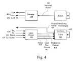
- FIG. 4is a more detailed block diagram of the connections between the controller 110 ( FIG. 2 ) and the laser driver 105 and post-amplifier 104 .
- Optical signals received by the optical receiver in the ROSA 102are transmitted along a received power connection 402 to the postamp 104 .
- the postamp 104generates a fixed output swing digital signal which is connected to the host, and/or controller 110 ( FIG. 2 ), via RX+ and RX ⁇ connections 404 .
- the postamp circuitalso provides a Loss of Signal (LOS) indicator to the host, and/or controller 110 ( FIG. 2 ), via a LOS connection 406 , indicating the presence or absence of suitably strong optical input.
- LOSLoss of Signal
- the hosttransmits signal inputs TX+ and TX ⁇ to the laser driver 105 via TX+ and TX ⁇ connections 420 .
- the controller 110( FIG. 2 ) transmits power to the laser driver via connection 416 , and a transmitter disable signal to the laser driver 105 via an internal TX disable connection 418 .
- a modulation currentis supplied to the laser 410 via an AC modulation current connection 414 .
- a DC laser bias currentis supplied from the laser driver 105 to the laser 410 via a laser bias current connection 412 .
- the level of the laser bias currentis adjusted to maintain proper laser output (i.e., to maintain a specified or predefined average level of optical output power by the TOSA 103 ) and to compensate for variations in temperature and power supply voltage.
- some transceiversinclude an output power monitor 422 within the TOSA 103 that monitors the energy output from the laser 410 .
- the output power monitor 422is preferably a photodiode within the laser package that measures light emitted from the back facet of the laser 410 .
- the amount of optical power produced by the back facet of the laser diode, represented by an output power signal,is directly proportional to the optical power output by the front or main facet of the laser 410 .
- the ratio, K, of the back facet optical power to the front facet optical powerwill vary from one laser diode to another, even among laser diodes of the same type.
- the output power signalis transmitted from the output power monitor 422 in the TOSA 103 to the controller 110 ( FIG. 2 ) via a transmitter output power connection 408 .
- certain of the components within the fiber optic transceiverinclude monitoring logic that outputs digital fault conditions.
- the laser driver 105may output a “out of lock” signal 424 if a control loop monitoring the modulation current is broken. These digital fault condition outputs may then be used to notify the host of fault conditions within the component, or shut down the laser.
- FIG. 5Ais a block diagram 500 of a high-resolution alarm system 502 and a fast trip alarm system 504 , for monitoring and controlling the operation of the fiber optic transceiver to ensure eye safety.
- the fast trip alarm system 504is used to quickly generate flag used to shut down the laser 410 ( FIG. 4 ).
- the fast trip alarm system 504uses an analog comparator 522 to achieve a quick response.
- the high resolution alarm system 502does not generate a flag to shut down the laser as quick as the fast trip alarm system 504 .
- the high resolution alarm system 502is more accurate than the fast trip alarm system 504 .
- the high resolution alarm system 502uses digital comparators 512 . In use, the high resolution alarm system 502 and the fast trip alarm system 504 operate simultaneously. If the fast trip alarm system 504 does not generate a flag quickly, the high resolution alarm system 502 will identify the fault and generate a flag to shut down the laser.
- the high-resolution alarm system 502 and fast trip alarm system 504are preferably contained within the controller 110 ( FIG. 3 ). Both the high-resolution alarm system 502 and fast trip alarm system 504 are coupled to an input signal 506 . In some embodiments this input signal is an analog signal. It should be noted that FIG. 5A shows the high-resolution alarm system 502 and fast trip alarm system 504 for a single input signal 506 . However, in some embodiments, identical alarm systems 502 and 504 are provided for each of several signals 506 , including several different types of input signals.
- the input signals processed by the alarm systems 502 and 504preferably include: power supply voltage, internal transceiver temperature (hereinafter “temperature”), laser bias current, transmitter output power, and received optical power.
- the power supply voltage 19( FIG. 3 ) is preferably the voltage in millivolts as measured by the Vcc sensor 126 ( FIG. 3 ).
- the temperatureis preferably the temperature in /C as measured by the temperature sensor 125 ( FIG. 3 ).
- the laser bias currentis preferably the laser bias current in microamps supplied to the laser 410 ( FIG. 4 ) via the laser bias current connection 412 ( FIG. 4 ).
- the received optical poweris the power in microwatts received at the ROSA 102 ( FIG. 4 ) via the received power connection 402 ( FIG. 4 ).
- the optical output power( FIG. 4 ) is the optical power output in microwatts, from the power monitor 422 ( FIG. 4 ) as received by the controller 110 ( FIG. 2 ) via the output power connection 408 ( FIG. 4
- the high-resolution alarm system 502preferably utilizes all of the above described input signals to trigger warnings and/or shut down at least part of the fiber optic transceiver. In other embodiments the high-resolution alarm system 502 utilizes a subset of the above described input signals to trigger warnings and/or alarms.
- the high-resolution alarm system 502includes one or more analog to digital converters 124 (see also FIG. 3 ) that are configured to receive the analog input signal 506 .
- Each type of analog input signalis preferably converted to a digital input signal using a calibration factor 508 for the particular type of input signal received. For example, a supply voltage in millivolts is converted to a 16 bit digital number by multiplying a supply voltage millivolt value by a supply voltage calibration factor.
- These calibration factorsare predetermined and are preferably stored in the diagnostic value and flag storage 128 ( FIG. 3 ). Alternatively, such calibration factors 508 may be stored in the general purpose EEPROM 120 ( FIG. 3 ).
- the analog to digital converter 124is also coupled to multiple comparators 512 .
- the comparators 512form a portion of the value comparison and other logic 131 ( FIG. 3 ) in the controller 110 ( FIG. 2 ).
- these comparators 512are digital comparators.
- high-resolution setpoints 5101 )-(N).
- four predetermined setpoints 510 ( 1 )-( 4 )are stored in the diagnostic value and flag storage 128 ( FIG. 3 ). These four predetermined setpoints are: a high alarm setpoint 510 ( 1 ), a high warning setpoint 510 ( 2 ), a low warning setpoint 510 ( 3 ), and a low alarm setpoint 510 ( 4 ).
- the comparators 512 ( 1 )-(N)are configured to compare the input signal 506 with the predetermined setpoints 510 ( 1 )-( 4 ).
- the digital equivalent of the input signal 506is simultaneously compared by the comparators 512 ( 1 )-(N), to each of the four digital predetermined setpoints 510 ( 1 )-(N) for the particular type of input signal received.
- the setpoints 510 ( 1 )-(N) and the digital equivalents to the input signals 506are sixteen bit numbers. Of course, in other embodiments there may be more or fewer setpoints 510 , and the setpoints 510 and input signal could be digitally represented by more or fewer than sixteen bits.
- the comparatorssubsequently generate high-resolution flags 514 ( 1 )-(N), which are input into the general logic and fault control circuit 133 ( FIG. 3 ) to either provide a warning to the host computer, or to shut down at least part of the fiber optic transceiver, such as the laser driver 105 ( FIG. 4 ) and/or laser 410 ( FIG. 4 ). Further details of the method for preventing potentially unsafe operation of the fiber optic transceiver, using the high-resolution alarm system 502 , are described below in relation to FIG. 7 .
- the fast trip alarm system 504includes multiple temperature dependant setpoints 516 . These temperature dependant setpoints 516 are preferably stored in the diagnostic values flag storage 128 ( FIG. 3 ) or the D/A temperature lookup tables 122 ( FIG. 3 ).
- a multiplexer 518is configured to supply one of the temperature dependant setpoints 516 to a digital to analog converter 123 (also shown in FIG. 3 ). The precise temperature dependant setpoint 516 that is supplied depends on the temperature 520 measured by the temperature sensor 125 ( FIG. 3 ). For example, for a first measured temperature, a first setpoint is supplied by the multiplexer 518 to the digital to analog converter 123 .
- a separate copy or instance of the fast trip alarm system 504is provided for each input signal 506 for which a temperature based alarm check is performed.
- the fast trip alarm system 504preferably utilizes only the following input signals 506 : laser bias current, transmitter output power, and received optical power input signals, and thus there are three instances of the fast trip alarm system 504 .
- fewer or more fast trip alarm systems 504may be employed.
- the analog input signals processed by the fast trip alarm systems 504are each fed to a respective comparator 522 that compares the input signal to an analog equivalent of one of the temperature dependant setpoints 516 .
- the comparators 522form a portion of the value comparison and other logic 131 ( FIG. 3 ) in the controller 110 ( FIG. 2 ).
- the comparators 522are analog comparators.
- At least eight temperature dependant setpoints 516are provided for the laser bias current input signal, with each setpoint corresponding to a distinct 16 /C. temperature range.
- the size of the operating temperature range for each setpointmay be larger or smaller in other embodiments.
- These temperature dependant setpoints for the laser bias currentare crucial because of the temperature compensation needs of a short wavelength module. In particular, at low temperatures the bias required to produce the required light output is much lower than at higher temperatures. In fact, a typical laser bias current when the fiber optic transceiver is at the high end of its temperature operating range will be two or three times as high as the laser bias current when fiber optic transceiver is at the low end of its temperature operating range, and thus the setpoints vary dramatically based on operating temperature.
- a typical temperature operating range of a fiber optic transceiveris about ⁇ 40° C. to about 85° C.
- the temperature dependant setpoints for the laser bias currentare also crucial because of the behavior of the laser bias circuit in a fiber optic transceiver that transmits long wavelength energy.
- At least four temperature dependant setpoints 516are provided for the received optical power and transceiver output power input signals, with each setpoint corresponding to a distinct 32 /C. operating temperature range of the fiber optic transceiver.
- the size of the operating temperature range for each setpointmay be larger or smaller in other embodiments.
- the comparator 522is configured to compare an analog equivalent of one of the setpoints 516 to the analog input signal 506 . In some embodiments, if the analog input signal 506 is larger than the analog equivalent to one of the setpoints 516 , then a fast trip alarm flag 524 is generated.
- the fast trip alarm flag 524is input into the general logic and fault control circuit 133 ( FIG. 3 ) to either provide a warning to the host computer or shut down at least part of the fiber optic transceiver, such as the laser driver 105 ( FIG. 4 ) and/or laser 410 ( FIG. 4 ). Further details of the method for preventing potentially unsafe operation of the fiber optic transceiver, using the fast trip alarm system 504 , are described below in relation to FIG. 6 .
- FIG. 5Bis a block diagram of logic 530 for disabling the operation of the fiber optic transceiver to ensure eye safety, according to an embodiment of the invention.
- the high-resolution alarm flags 514 ( 1 )-( 4 ), the fast trip alarm system flag 524 , and any digital fault condition 532 signals, from FIGS. 4 and 5Aare transmitted to an OR gate 534 , which is used to shut down the laser. This is accomplished by sending a signal along the internal Tx disable line 418 ( FIG. 4 ). For example if a digital “out of lock” signal or a fast trip alarm flag is received, the laser will be shut down. It should be appreciated that more or less alarm flags or digital fault condition signals may be supplied to the OR gate 534 .
- the inputs to the OR gate 534include only the high and low alarm flags 514 ( 1 ), 514 ( 4 ), the fast trip alarm flag 524 and the digital fault condition(s) signal 532 .
- the warning flags 514 ( 2 ) and 514 ( 3 )are not used to generate the internal Tx disable signal 418 .
- FIG. 6is a flow chart of a method 600 for reducing or preventing potentially unsafe operation of a fiber optic transceiver using the fast trip alarm system 504 of FIG. 5A .
- an input signalis acquired, at step 604 .
- the input signalis preferably an analog signal of: laser bias current in milliamps, received optical power in microwatts, or transceiver output power in microwatts.
- a temperature of the fiber optic transceiveris obtained at step 606 . Step 606 may be performed before, after or at the same time as input signal acquisition step 604 .
- the multiplexer 518uses the input signal and the measured temperature to determine, at step 608 , which setpoint 516 ( FIG. 5A ) to use for comparison with the input signal. For example, if the input signal is laser bias current, then the multiplexer looks up a setpoint for laser bias current based on the obtained temperature 520 ( FIG. 5A ).
- this setpointis then converted from a digital to analog value, at step 610 by the digital to analog converter 123 ( FIG. 5A ). Thereafter, the comparator 522 ( FIG. 5A ) compares the input signal to the setpoint, at step 612 , to determine whether there is a conflict, at step 614 . In some embodiments, a conflict occurs where the input signal is higher than the setpoint (or an analog equivalent of the setpoint). Alternatively, a conflict may occur where the input signal is lower than the setpoint (or an analog equivalent of the setpoint).
- a fast trip alarm flag 524( FIG. 5A ) is generated at step 616 .
- the fast trip alarm flag 524( FIG. 5A ) is then used to shut down at least part of the fiber optic transceiver, at step 618 , by applying a signal to the internal TxDisable connection 418 ( FIG. 4 ).
- the fast trip alarm flag 524( FIG. 5A ) is used to disable the laser driver 105 ( FIG. 4 ) and/or laser 410 ( FIG. 4 ), so that no potential eye-damage can occur.
- the alarm flag 524( FIG. 5A ) can be used to control the laser driver via the internal Tx Disable Output (Dout) and signal the fault to the host system via the Tx Fault Output (Fout). These outputs can also respond to the Tx Fault Input (Fin), if that signal exists in any given implementation, and the Tx Disable Input (Din) which comes into the fiber optic transceiver from the host.
- DoutTx Disable Output
- FoutTx Fault Output
- FIG. 7is a flow chart of a method 700 for reducing or preventing potentially unsafe operation of a fiber optic transceiver using the high-resolution alarm system 502 of FIG. 5A .
- an input signalis acquired, at step 704 .
- the input signalis preferably an analog signal of: power supply voltage 19 ( FIG. 3 ) in millivolts; the temperature in /C.; the laser bias current 412 ( FIG. 4 ) in microamps; the received optical power 420 ( FIG. 4 ) in microwatts; and the output power 408 ( FIG. 4 ) in microwatts.
- the input signal(s)may be scaled in accordance with other units.
- An analog to digital converter 124( FIGS. 3 and 5 ) then converts the analog input signal 506 ( FIG. 5A ) to a digital equivalent, preferably a 16 bit number, at step 706 .
- Conversion of the analog input signal 506 ( FIG. 5A ) to a digital equivalent performedincludes multiplying the input signal 506 ( FIG. 5A ) by a calibration factor 508 ( FIG. 5A ), at step 708 , for the particular type of input signal received, as described above in relation to FIG. 5A .
- the comparators 512( FIG. 5A ) then compare the digital equivalent of the input signal to the setpoints 510 ( 1 )-(N) ( FIG. 5A ), at step 710 , to determine whether there is a conflict.
- conflictsoccur when the digital equivalent of the input signal is: higher than the high alarm setpoint 510 ( 1 ) to produce a high-alarm flag 514 ( 1 ) ( FIG. 5A ); higher than the high warning setpoint 510 ( 2 ) ( FIG. 5A ) to produce a high warning flag 514 ( 2 ) ( FIG. 5A ); lower than a low warning flag 510 ( 3 ) ( FIG. 5A ) to produce a low warning flag 514 ( 3 ) ( FIG.
- the method 700repeats itself. However, if a conflict does exist ( 714 —Yes), then a high-resolution flag 514 ( 1 )-(N) ( FIG. 5A ) is generated, at step 714 .
- the high-resolution flags 514 ( 1 )-(N) ( FIG. 5A )are a high alarm flag 514 ( 1 ), a high warning flag 514 ( 2 ), a low warning flag 514 ( 3 ), and a low alarm flag 514 ( 4 ), as shown in FIG. 5A . Also In some embodiments, the high alarm flag 514 ( 1 ) ( FIG.
- the part of the fiber optic transceiver shut downpreferably includes the laser driver 105 ( FIG. 4 ) and/or the TOSA 103 ( FIG. 4 ).
- the high and low warning flags 514 ( 2 ) and 514 ( 3 ) ( FIG. 5A )preferably merely provide a warning to the host and do not shut down the laser driver 105 ( FIG. 4 ) and/or the TOSA 103 ( FIG. 4 ).
- the alarm flags 514 ( 1 )-(N)can be used to control the laser driver via the internal Tx Disable Output (Dout) and signal the fault to the host system via the Tx Fault Output (Fout). These outputs can also respond to the Tx Fault Input (Fin), if that signal exists in any given implementation, and the Tx Disable Input (Din) which comes into the fiber optic transceiver from the host.
- the high-resolution alarm system 502updates the high-resolution alarm flags at a rate of approximately once every 0.015 seconds (15 milliseconds), and more generally at least 50 times per second. Thus, the high-resolution alarm flags are set within 0.015 seconds of the detection of an alarm condition. In some embodiments the high-resolution alarm flag update rate is between about 50 times per second and 200 times per second. However, the fast trip alarm system 504 ( FIG. 5A ) preferably updates the fast trip alarm flags a rate that is faster than once every 10 microseconds.
- the fast trip alarm system 504updates the fast trip alarm flags at a rate that is between 50,000 and 200,000 times per second, and more generally at least 50,000 times per second. In some embodiments, the alarm flags of the fast trip alarm system 504 are updated at a rate that is more than a thousand times faster than the update rate of the high-resolution alarm flags. In other embodiments the alarm flags of the fast trip alarm system 504 are updated at a rate that is between 250 and 4000 times faster than the update rate of the high-resolution alarm flags.
- the power monitor 422( FIG. 4 ) in a fiber optic transceiver that includes a power monitor, or its associated circuitry, fails, indicating no or low output power when the laser is in fact operating.
- the laser bias driverwill attempt to increase the transmitter output power by increasing laser bias current. Since the feedback is interrupted, the laser is driven to its maximum capability, perhaps exceeding the eye safety alarm setpoints.
- the fast trip alarm flagwill be generated in less than 10 microseconds after the failure and this fast trip alarm flag can be used to shut down the laser driver via the internal Tx disable (Dout) output. If the fast trip alarm fails or is not selected in the output logic setup, the high-resolution alarm for laser bias current is generated, and the high-resolution low alarm for power would also occur, either of which could be used to shut down the laser driver and/or TOSA.
- the laser driverin all types of fiber optic transceiver, or its associated circuitry fails, driving the laser to its maximum output.
- the laser bias currentmay read zero or very high, and in a fiber optic transceiver that includes a power monitor, the power will read very high.
- the fast trip alarm for laser bias current, and the fast trip alarm for transmitted output powerwill generate an alarm flag within 10 microseconds. If the laser bias current is reading zero, the high-resolution low alarm for laser bias current will generate an alarm flag. This may be indistinguishable from a failure that causes zero light output, like an open laser wire or shorted laser, but the alarm systems preferably err on the side of safety and command the laser to shut down.
- the logicmay not be possible for the logic to physically turn the laser off, if, for example, the fault was caused by a shorted bias driver transistor. In any case, the link will be lost and the Tx fault output will be asserted to advise the host system of the failure.
- the bias driver circuitthere are non-error conditions which could set some of these flags during a host-commanded transmit disable state, or during startup conditions. For example, if the host commands a transmitter shutdown, some circuits might read zero transmit power, as one would expect, and some might read very large transmit power as an artifact of the shutdown mechanism.
- the laserWhen the laser is re ⁇ enabled, it takes a period of time for the control circuitry to stabilize, and during this time there may be erratic occurrences of both low, high and fast trip alarms.
- Programmable delay timersare preferably used to suppress the fault conditions during this time period.
- FIG. 8is a block diagram of another controller IC 800 .
- the controller IC 800is identical in all respects to the controller 300 shown in FIG. 3 , except that an analog to digital signal conditioning module, also called ADC module 802 , replaces the ADC 127 ( FIG. 3 ). Accordingly, all of the reference numerals in FIG. 8 , except for 800 and 802 , refer to the same components described above in relation to FIG. 3 .
- the ADC module 802greatly enhances the utility of the ADC 127 , giving it greater precision and accuracy.
- FIG. 9is a block diagram of the ADC module 802 shown in FIG. 8 . It should be appreciated that the ADC module 802 may contain more or fewer components than those described below. For example, the A/D input multiplexer 124 ( FIGS. 3 and 8 ) may be incorporated into the ADC module 802 .
- Analog signals 902are received by the ADC module 802 .
- the analog signalsare monitoring signals that represent operating conditions in a transmitter, receiver or transceiver.
- the ADC module 802converts the analog signals into digital signals that have been scaled and offset so as to represent operating condition measurements having predefined measurement units.
- the analog signals received by the ADC module 802include signals representing laser bias current, received optical power, output optical power, power supply voltage and temperature.
- the analog signalsare a subset of these signals, and in some embodiments additional analog signals are received by the module 802 .
- the digital signals produced by the ADC module 802include signals representing laser bias current in milliamps, received optical power in microwatts, output optical power in microwatts, power supply voltage in millivolts and temperature in degrees C. More generally, the analog signals received by the ADC module 802 and corresponding digital signals produced by the ADC module 802 include signals representing measurements of light, power, currents and/or voltages within an optoelectronic device.
- the digital signals produced by the ADC moduleare stored in memory mapped locations within diagnostic value and flag storage 128 , thereby making these signals available to a host device at memory mapped locations. More generally, the digital signals are stored in memory mapped locations that can be read by a host device through the execution of read commands to the memory mapped locations.
- the operation of the ADC module 802is controlled by values stored in a set of registers or other storage devices 905 .
- the registersare memory mapped, enabling the ADC module 802 to be calibrated during manufacture by storing calibration values in the registers 905 .
- the registers 905are a register bank or register array or other storage device that outputs values in accordance with a signal ID value that corresponds to the current analog input signal 902 .
- the signal ID valuemay be the same value that is used by the A/D input mux 124 ( FIG. 8 ) to select the analog signal to be passed to the ADC module 802 .
- calibration valuesare dynamically loaded into the registers 905 by control circuitry from general purpose EEPROM 120 or another other memory device.
- the registers 905themselves are non-volatile memory devices that are separate from, or that comprise a portion of, the EEPROM 120 .
- the registers 905are memory mapped locations which can be read by a host device.
- the registers 905are memory mapped locations which can be written by a host device having an appropriate password or other mechanism for enabling it to write into those memory mapped locations.
- one or more of the values provided by registers 905 to the ADC module 802may be temperature compensated values, which vary in accordance the temperature in the device being monitored.
- the temperature compensated valuesmay be produced by a table look up operation, or may be computed, for instance by a microcontroller or microprocessor.
- the ADC module 802includes gain circuitry 904 , an ADC 906 , offset circuitry 908 and shifting circuitry 910 .
- the gain circuitry 904is preferably programmable and configured to amplify or attenuate an analog signal by a gain value into an analog gain signal.
- the gain valueis preferably controlled by a digital gain control signal 914 received from registers 905 or from another storage device.
- the gain circuitry 904makes it possible to calibrate the analog signals to achieve a desired LSB or full-scale voltage of the ADC 906 .
- the gain circuitrymakes it possible to internally amplify small input signals in order to maximize the use of the ADC.
- the gain circuitry 904amplifies the analog signal by a factor of sixteen or less.
- the ADC 906is similar to the ADC 127 described above in relation to FIG. 3 .
- the ADC 906is a 12-bit ADC, which generates an output value having 12 bits plus a sign bit.
- the values generated by the ADC 906are output left justified as 2 byte (16 bit) values, ranging from 0000h to FFF8h.
- the offset circuitry 908internally adjusts the digital signal by adding either a positive or a negative offset value.
- the offset valueis received from registers 905 , as explained above.
- the offset circuitry 908is configured so as to clamp positive values at a first predefined digital value (e.g., FFF8h), and to clamp negative values at a second predefined digital value (e.g., 0000h). It is noted that the adjustment performed by the offset circuitry 908 , unless zero, affects the full-scale digital output at either the high or low end of the input signal range. For instance, a negative adjustment at the offset circuitry 908 will reduce the maximum output value of the ADC module 802 .
- the digital signal adjusted by the offset circuitry 908is then shifted by the shifting circuitry 910 , which is preferably programmable and configured to shift the digital signal either left or right into a digital shifted signal based on a shift value.
- the shifting circuitry 910is programmable and configured to right shift the digital signal into a digital shifted signal that is shifted to the right, based on a shift value.
- the shift valueis preferably controlled by a digital shift control signal 918 received from registers 905 .
- the shift circuitryshifts the digital signal by zero to four bits (right or left), based on the control signal 918 . Setting the control signal 918 to zero disables the shifting circuitry 910 . It is noted that shifting affects the full-scale digital output. For example, if set to 2 right shifts, the full-scale digital output becomes 3FFEh.
- the digital valueis then written to the appropriate memory mapped location, for example a memory mapped location within the diagnostic value and flag storage 128 ( FIG. 8 ).
- the analog signal 902is a sequence of analog input signals representing a set of operating conditions of an optoelectronic device.
- the Signal ID that controls the A/D muxis periodically rotated through a set of values, thereby periodically routing a sequence of analog signals through the ADC module 802 .
- the ADC module 802is simultaneously configured by control values from register 905 to process each of the analog signals in accordance with a respective set of control values. Each set of control values corresponds to the operating condition represented by the analog signal being processed.
- the resulting digital signalsare stored in memory, or more generally in memory mapped locations.
- the digital signalsare also compared with limit values and the resulting flag values are also stored in memory or other memory mapped locations.
- the digital values and flag valuesare accessible via an interface to a host device, which sends read commands that specify the memory mapped locations to be read by the host device.
- the adjustment circuitry of the ADC module 802is particularly beneficial when the signal to be monitored is small and, therefore, not making use of the entire ADC range.
- By amplifying the analog signal in the gain circuitry 904 before the analog to digital conversion, and then dividing it back down by the same (or a similar) factor using the shifting circuit 910the desired LSB is preserved and both precision and accuracy are improved.
- the analog signal(e.g., a signal representing received optical power) swings between 0V to 0.5V
- the ADC circuitryis initially factory calibrated such that each of the analog input signals are factory trimmed to a full scale voltage of 2.5V.
- the default gain valueis 1
- the default offset valueis zero
- the default shifting valueis 0. Since the calibrated full signal swing is 2.5V, the ADC module will have a resolution of 610 ⁇ V (2.5V/4096) for a 12-bit ADC.
- a signal having a maximum swing of 0.5Vwill use only one fifth of the available range and will still have a resolution of 610 ⁇ V.
- the gainis set to four, and the shifting value is set to two (to the right, thereby resulting in a division by four).
- precisionis increased.
- the full-scale voltageis now 0.625V (2.5V/4), which is sufficient to cover the full 0 to 0.5V range of the input signal, and the resolution is now 152.5 ⁇ V (2.5V/16384), which is a substantial improvement over 610 ⁇ V.
- the ADC module 802enhances the precision and accuracy of the digitized signal values produced by the ADC 906 .
- the ADC module's internal calibrationpreferably features both programmable gain circuitry and programmable offset circuitry, eliminating the need for external signal conditioning circuitry.
- the input signalcan be amplified or attenuated to make use of the entire range, or at least a larger portion of the range, of the ADC.
- shiftingcan be used to scale (divide) the digital output up or down so that the desired Least Significant Bit (LSB) of a measured operating characteristic remains unaffected and even transparent to the user of the optoelectronic transceiver.
- LSBLeast Significant Bit
- a digital offset 908( FIG. 9 ) is provided between the ADC 906 ( FIG. 9 ) and the shifting circuitry 910 ( FIG. 9 )
- an analog offsetmay replace or supplement the digital offset 908 ( FIG. 9 ).
- the analog offsetmay be located at any point in the analog domain prior to the ADC 906 ( FIG. 9 ), but is preferably situated between the gain circuitry 904 ( FIG. 9 ) and the ADC 906 ( FIG. 9 ).
- the analog offsetmay apply either positive or negative analog offset to the analog signal based on an offset value (either analog or digital) 916 ( FIG. 9 ), as described above.
- the present inventionis applicable to transmitters and receivers, and thus is not solely applicable to transceivers.
- the controller of the present inventionis suitable for application in multichannel optical links.
- 6Fh A/D UpdatedAllows the user to verify if an update from the A/D has occurred to the 5 values: temperature, Vcc, B in , P in and R in .
- the userwrites the byte to 00h. Once a conversion is complete for a give value, its bit will change to ‘1’.
- 70h-73h Alarm FlagsThese bits reflect the state of the alarms as a conversion updates. High alarm bits are ‘1’ if converted value is greater than corresponding high limit. Low alarm bits are ‘1’ if converted value is less than corresponding low limit. Otherwise, bits are 0b. 74h-77h Warning Flags These bits reflect the state of the warnings as a conversion updates. High warning bits are ‘1’ if converted value is greater than corresponding high limit.
- A0h-A1h P in High Alarm R in High Alarm 82h-83h Temperature LowThe value written to this location serves as the 8Ah-8Bh Alarm low alarm limit.
- Data formatis the same as the 92h-93h Vcc Low Alarm corresponding value (temperature, Vcc, B in, P in 9Ah-9Bh B in Low Alarm R in ).
- A2h-A3h P in Low Alarm R in Low Alarm 84h-85h Temp High WarningThe value written to this location serves as the 8Ch-8Dh Vcc High Warning high warning limit.
- Data formatis the same as 94h-95h B in High Warning the corresponding value (temperature, Vcc, B in, 9Ch-9Dh P in High Warning P in R in ).
- Memory Location(Array 0) Name of Location Function A4h-A5h R in High Warning 86h-87h Temperature Low The value written to this location serves as the 8Eh-8Fh Warning low warning limit. Data format is the same as 96h-97h Vcc Low Warning the corresponding value (temperature, Vcc, B in, 9Eh-9Fh B in Low Warning P in R in ). A6h-A7h P in Low Warning R in Low Warning A8h-AFh, D out control 0-8 Individual bit locations are defined in Table 4.
- C2h D out DelaySelects number of prescale clocks
- CEh-CFh R in —A/D Scale D0h Chip AddressSelects chip address when external pin ASEL is low.
- PW1 Byte 3 (D3h)The four bytes are used for password 1 entry. MSB The entered password will determine the PW1 Byte 2 (D4h) Finisar customer's read/write privileges. PW1 Byte 1 (D5h) PW1 Byte 0 (D6h) LSB Memory Location (Array 3, cont) Name of Location Function of Location D7h D/A Control This byte determines if the D/A outputs source or sink current, and it allows for the outputs to be scaled.
- D8h-DFh B in Fast TripThese bytes define the fast trip comparison over temperature.
- E0h-E3h P in Fast TripThese bytes define the fast trip comparison over temperature.
- E4h-E7h R in Fast TripThese bytes define the fast trip comparison over temperature.
- E8h Configuration Location of the bitsis defined in Table 4 Override Byte E9h Reserved Reserved EAh-EBh Internal State Bytes Location of the bits is defined in Table 4 ECh I/O States 1 Location of the bits is defined in Table 4 EDh-EEh D/A Out Magnitude of the temperature compensated D/A outputs EFh Temperature Index Address pointer to the look-up Arrays F0h-FFh Reserved Reserved Memory Location (Array 4) Name of Location Function of Location 00h-FFh D/A Current vs. Temp #1 (User-Defined Look-up Array #1) Memory Location (Array 5) Name of Location Function of Location 00h-FFh D/A Current vs. Temp #2 (User-Defined Look-up Array #2)
Landscapes
- Physics & Mathematics (AREA)
- Electromagnetism (AREA)
- Engineering & Computer Science (AREA)
- Computer Networks & Wireless Communication (AREA)
- Signal Processing (AREA)
- Optical Communication System (AREA)
- Analogue/Digital Conversion (AREA)
Abstract
Description
- Setup functions. These generally relate to the required adjustments made on a part-to-part basis in the factory to allow for variations in component characteristics such as laser diode threshold current.
- Identification. This refers to general purpose memory, typically EEPROM (electrically erasable and programmable read only memory) or other nonvolatile memory. The memory is preferably accessible using a serial communication bus in accordance with an industry standard. The memory is used to store various information identifying the transceiver type, capability, serial number, and compatibility with various standards. While not standard, it would be desirable to further store in this memory additional information, such as sub-component revisions and factory test data.
- Eye safety and general fault detection. These functions are used to identify abnormal and potentially unsafe operating parameters and to report these to the user and/or perform laser shutdown, as appropriate.
- Temperature compensation functions. For example, compensating for known temperature variations in key laser characteristics such as slope efficiency.
- Monitoring functions. Monitoring various parameters related to the transceiver operating characteristics and environment. Examples of parameters that it would be desirable to monitor include laser bias current, laser output power, received power level, supply voltage and temperature. Ideally, these parameters should be monitored and reported to, or made available to, a host device and thus to the user of the transceiver.
- Power on time. It would be desirable for the transceiver's control circuitry to keep track of the total number of hours the transceiver has been in the power on state, and to report or make this time value available to a host device.
- Margining. “Margining” is a mechanism that allows the end user to test the transceiver's performance at a known deviation from ideal operating conditions, generally by scaling the control signals used to drive the transceiver's active components.
- Other digital signals. It would be desirable to enable a host device to be able to configure the transceiver so as to make it compatible with various requirements for the polarity and output types of digital inputs and outputs. For instance, digital inputs are used for transmitter disable and rate selection functions while digital outputs are used to indicate transmitter fault and loss of signal conditions.
- Class I: These devices are considered inherently safe. The IEC requires a classification label, but the CDRH does not.
- Class II:
Class 2 lasers have levels similar to a Class I device for an exposure of 0.25 second. Eye protection is normally provided by what is called a “normal aversion response.” This means that a victim usually responds to an exposure by an involuntary blink of the eye. - Class III: Both the CDRH and IEC define two subclasses: IIIa and IIIb. Class IIIa devices cannot injure a person's eye under normal conditions of bright light. They can, however, injure eyes when viewed through an optical aid such as a microscope or telescope. For Class IIIa, the CDRH concerns only visible light, while the IEC includes all wavelengths. Class IIIb devices can injure the eye if the light is viewed directly.
- Class IV. These devices are more powerful than even Class IIIb lasers. They can injure the eye even when viewed indirectly.
| TABLE 1 |
| MEMORY MAP FOR TRANSCEIVER CONTROLLER |
| Memory | |||
| Location | |||
| (Array 0) | Name of Location | Function | |
| 00h-5Fh | IEEE Data | This memory block is used to store required | |
| GBIC data | |||
| 60h | Temperature MSB | This byte contains the MSB of the 15- | |
| complement temperature output from the | |||
| temperature sensor. | |||
| 61h | Temperature LSB | This byte contains the LSB of the 15- | |
| complement temperature output from the | |||
| temperature sensor. | |||
| (LSB is 0b). | |||
| 62h-63h | VccValue | These bytes contain the MSB (62h) and the | |
| LSB (63h) of the measured Vcc | |||
| (15-bit number, with a 0b LSbit) | |||
| 64h-65h | BinValue | These bytes contain the MSB (64h) and the | |
| LSB (65h) of the measured Bin | |||
| (15-bit number, with a 0b LSbit) | |||
| 66h-67h | PinValue | These bytes contain the MSB (66h) and the | |
| LSB (67h) of the measured Pin | |||
| (15-bit number, with a 0b LSbit) | |||
| 68h-69h | RinValue | These bytes contain the MSB (68h) and the | |
| LSB (69h) of the measured Rin | |||
| (15-bit number, with a 0b LSbit) | |||
| 6Ah-6Dh | Reserved | Reserved | |
| 6Eh | IO States | This byte shows the logical value of the I/O | |
| pins. | |||
| 6Fh | A/D Updated | Allows the user to verify if an update from the | |
| A/D has occurred to the 5 values: temperature, | |||
| Vcc, Bin, Pinand Rin. The user writes the byte | |||
| to 00h. Once a conversion is complete for a | |||
| give value, its bit will change to ‘1’. | |||
| 70h-73h | Alarm Flags | These bits reflect the state of the alarms as a | |
| conversion updates. High alarm bits are ‘1’ if | |||
| converted value is greater than corresponding | |||
| high limit. Low alarm bits are ‘1’ if converted | |||
| value is less than corresponding low limit. | |||
| Otherwise, bits are 0b. | |||
| 74h-77h | Warning Flags | These bits reflect the state of the warnings as a | |
| conversion updates. High warning bits are ‘1’ | |||
| if converted value is greater than | |||
| corresponding high limit. Low warning bits | |||
| are ‘1’ if converted value is less than | |||
| corresponding low limit. Otherwise, bits are | |||
| 0b. | |||
| 78h-7Ah | Reserved | Reserved | |
| 7Bh-7Eh | Password Entry Bytes | The four bytes are used for password entry. | |
| PWE Byte 3 (7Bh) | The entered password will determine the user's | ||
| MSByte | read/write privileges. | ||
| PWE Byte 2 (7Ch) | |||
| PWE Byte 1 (7Dh) | |||
| PWE Byte 0 (7Eh) | |||
| LSByte | |||
| 7Fh | Array Select | Writing to this byte determines which of the | |
| upper pages of memory is selected for reading | |||
| and writing. | |||
| 0xh (Array x Selected) | |||
| Where x = 1, 2, 3, 4 or 5 | |||
| 80h-F7h | Customer EEPROM | ||
| 87h | DA % Adj | Scale output of D/A converters by specified | |
| percentage | |||
| Memory | |||
| Location | |||
| (Array 1) | Name of Location | Function of Location | |
| 00h-FFh | Data EEPROM | ||
| Memory | |||
| Location | |||
| (Array 2) | Name of Location | Function of Location | |
| 00h-FFh | Data EEPROM | ||
| Memory | |||
| Location | |||
| (Array 3) | Name of Location | Function of Location | |
| 80h-81h | Temperature High | The value written to this location serves as the | |
| 88h-89h | Alarm | high alarm limit. Data format is the same as | |
| 90h-91h | Vcc High Alarm | the corresponding value (temperature, Vcc, Bin, | |
| 98h-99h | BinHigh Alarm | PinRin). | |
| A0h-A1h | PinHigh Alarm | ||
| RinHigh Alarm | |||
| 82h-83h | Temperature Low | The value written to this location serves as the | |
| 8Ah-8Bh | Alarm | low alarm limit. Data format is the same as the | |
| 92h-93h | Vcc Low Alarm | corresponding value (temperature, Vcc, Bin,Pin | |
| 9Ah-9Bh | BinLow Alarm | Rin). | |
| A2h-A3h | PinLow Alarm | ||
| RinLow Alarm | |||
| 84h-85h | Temp High Warning | The value written to this location serves as the | |
| 8Ch-8Dh | Vcc High Warning | high warning limit. Data format is the same as | |
| 94h-95h | BinHigh Warning | the corresponding value (temperature, Vcc, Bin, | |
| 9Ch-9Dh | PinHigh Warning | PinRin). | |
| Memory | |||
| Location | |||
| (Array 0) | Name of Location | Function | |
| A4h-A5h | RinHigh Warning | ||
| 86h-87h | Temperature Low | The value written to this location serves as the | |
| 8Eh-8Fh | Warning | low warning limit. Data format is the same as | |
| 96h-97h | Vcc Low Warning | the corresponding value (temperature, Vcc, Bin, | |
| 9Eh-9Fh | BinLow Warning | PinRin). | |
| A6h-A7h | PinLow Warning | ||
| RinLow Warning | |||
| A8h-AFh, | Doutcontrol 0-8 | Individual bit locations are defined in Table 4. | |
| C5h | Foutcontrol 0-8 | ||
| B0h-B7h, | Loutcontrol 0-8 | ||
| C6h | |||
| B8h-BFh, | |||
| C7h | |||
| C0h | Reserved | Reserved | |
| C1h | Prescale | Selects MCLK divisor for X-delay CLKS. | |
| C2h | DoutDelay | Selects number of prescale clocks | |
| C3h | FoutDelay | ||
| C4h | LoutDelay | ||
| C8h-C9h | Vcc—A/ | 16 bits of gain adjustment for corresponding | |
| CAh-CBh | Bin—A/D Scale | A/D conversion values. | |
| CCh-CDh | Pin—A/D Scale | ||
| CEh-CFh | Rin—A/D Scale | ||
| D0h | Chip Address | Selects chip address when external pin ASEL | |
| is low. | |||
| Margin # | 2 | Finisar Selective Percentage (FSP) for D/ | |
| Margin # | 1 | Finisar Selective Percentage (FSP) for D/ | |
| D3h-D6h | PW1 Byte 3 (D3h) | The four bytes are used for | |
| MSB | The entered password will determine the | ||
| PW1 Byte 2 (D4h) | Finisar customer's read/write privileges. | ||
| PW1 Byte 1 (D5h) | |||
| PW1 Byte 0 (D6h) | |||
| LSB | |||
| Memory Location | |||
| ( | Name of Location | Function of Location | |
| D7h | D/A Control | This byte determines if the D/A outputs | |
| source or sink current, and it allows for the | |||
| outputs to be scaled. | |||
| D8h-DFh | BinFast Trip | These bytes define the fast trip comparison | |
| over temperature. | |||
| E0h-E3h | PinFast Trip | These bytes define the fast trip comparison | |
| over temperature. | |||
| E4h-E7h | RinFast Trip | These bytes define the fast trip comparison | |
| over temperature. | |||
| E8h | Configuration | Location of the bits is defined in Table 4 | |
| Override Byte | |||
| E9h | Reserved | Reserved | |
| EAh-EBh | Internal State Bytes | Location of the bits is defined in Table 4 | |
| ECh | I/ | Location of the bits is defined in Table 4 | |
| EDh-EEh | D/A Out | Magnitude of the temperature compensated | |
| D/A outputs | |||
| EFh | Temperature Index | Address pointer to the look-up Arrays | |
| F0h-FFh | Reserved | Reserved | |
| Memory Location | |||
| (Array 4) | Name of Location | Function of Location | |
| 00h-FFh | D/A Current vs. | ||
| Temp #1 | |||
| (User-Defined Look-up Array #1) | |||
| Memory Location | |||
| (Array 5) | Name of Location | Function of Location | |
| 00h-FFh | D/A Current vs. | ||
| Temp #2 | |||
| (User-Defined Look-up Array #2) | |||
| TABLE 2 |
| DETAIL MEMORY DESCRIPTIONS - A/D VALUES AND STATUS |
| BITS |
| Byte | Bit | Name | Description |
| Converted analog values. Calibrated 16 bit data. (See Notes 1-2) |
| 96 | All | Temperature MSB | Signed 2's complement integer temperature (−40 to |
| (60h) | +125 C.) | ||
| Based on internal temperature measurement | |||
| 97 | All | Temperature LSB | Fractional part of temperature (count/256) |
| 98 | All | Vcc MSB | Internally measured supply voltage in transceiver. |
| Actual voltage is full 16 bit value * 100 uVolt. | |||
| 99 | All | Vcc LSB | (Yields range of 0-6.55 V) |
| 100 | All | TX Bias MSB | Measured TX Bias Current in mA Bias current is |
| full 16 bit value *(1/256) mA. | |||
| 101 | All | TX Bias LSB | (Full range of 0-256 mA possible with 4 uA |
| resolution) | |||
| 102 | All | TX Power MSB | Measured TX output power in mW. Output is |
| full 16 bit value *(1/2048) mW. (see note 5) | |||
| 103 | All | TX Power LSB | (Full range of 0-32 mW possible with 0.5 μW |
| resolution, or −33 to +15 dBm) | |||
| 104 | All | RX Power MSB | Measured RX input power in mW RX power is |
| full 16 bit value *(1/16384) mW. (see note 6) | |||
| 105 | All | RX Power LSB | (Full range of 0-4 mW possible with 0.06 μW |
| resolution, | |||
| or −42 to +6 dBm) | |||
| 106 | All | Reserved MSB | Reserved for 1stfuture definition of digitized analog |
| input | |||
| 107 | All | Reserved LSB | Reserved for 1stfuture definition of digitized analog |
| input | |||
| 108 | All | Reserved MSB | Reserved for 2ndfuture definition of digitized analog |
| input | |||
| 109 | All | Reserved LSB | Reserved for 2ndfuture definition of digitized analog |
| input |
| General Status Bits |
| 110 | 7 | TX Disable | Digital state of the TX Disable Input Pin |
| 110 | 6 | Reserved | |
| 110 | 5 | Reserved | |
| 110 | 4 | Rate Select | Digital state of the SFP Rate Select Input Pin |
| 110 | 3 | Reserved | |
| 110 | 2 | TX Fault | Digital state of the TX Fault Output Pin |
| 110 | 1 | LOS | Digital state of the LOS Output Pin |
| 110 | 0 | Power-On-Logic | Indicates transceiver has achieved power up and |
| data valid | |||
| 111 | 7 | Temp A/D Valid | Indicates A/D value in Bytes 96/97 is valid |
| 111 | 6 | Vcc A/D Valid | Indicates A/D value in Bytes 98/99 is valid |
| 111 | 5 | TX Bias A/D Valid | Indicates A/D value in Bytes 100/101 is valid |
| 111 | 4 | TX Power A/D | Indicates A/D value in Bytes 102/103 is valid |
| Valid | |||
| 111 | 3 | RX Power A/D | Indicates A/D value in Bytes 104/105 is valid |
| Valid | |||
| 111 | 2 | Reserved | Indicates A/D value in Bytes 106/107 is valid |
| 111 | 1 | Reserved | Indicates A/D value in Bytes 108/109 is valid |
| 111 | 0 | Reserved | Reserved |
| TABLE 3 |
| DETAIL MEMORY DESCRIPTIONS - ALARM AND WARNING FLAG BITS |
| Alarm and Warning Flag Bits |
| Byte | Bit | Name | Description |
| 112 | 7 | Temp High Alarm | Set when internal temperature exceeds high |
| alarm level. | |||
| 112 | 6 | Temp Low Alarm | Set when internal temperature is below low |
| alarm level. | |||
| 112 | 5 | Vcc High Alarm | Set when internal supply voltage exceeds high |
| alarm level. | |||
| 112 | 4 | Vcc Low Alarm | Set when internal supply voltage is below low |
| alarm level. | |||
| 112 | 3 | TX Bias High Alarm | Set when TX Bias current exceeds high alarm |
| level. | |||
| 112 | 2 | TX Bias Low Alarm | Set when TX Bias current is below low alarm |
| level. | |||
| 112 | 1 | TX Power High Alarm | Set when TX output power exceeds high alarm |
| level. | |||
| 112 | 0 | TX Power Low Alarm | Set when TX output power is below low alarm |
| level. | |||
| 113 | 7 | RX Power High | Set when Received Power exceeds high alarm |
| Alarm | level. | ||
| 113 | 6 | RX Power Low Alarm | Set when Received Power is below low alarm |
| level. | |||
| 113 | 5-0 | Reserved Alarm | |
| 114 | All | Reserved | |
| 115 | All | Reserved | |
| 116 | 7 | Temp High Warning | Set when internal temperature exceeds high |
| warning level. | |||
| 116 | 6 | Temp Low Warning | Set when internal temperature is below low |
| warning level. | |||
| 116 | 5 | Vcc High Warning | Set when internal supply voltage exceeds high |
| warning level. | |||
| 116 | 4 | Vcc Low Warning | Set when internal supply voltage is below low |
| warning level. | |||
| 116 | 3 | TX Bias High | Set when TX Bias current exceeds high warning |
| Warning | level. | ||
| 116 | 2 | TX Bias Low Warning | Set when TX Bias current is below low warning |
| level. | |||
| 116 | 1 | TX Power High | Set when TX output power exceeds high |
| Warning | warning level. | ||
| 116 | 0 | TX Power Low | Set when TX output power is below low warning |
| Warning | level. | ||
| 117 | 7 | RX Power High | Set when Received Power exceeds high warning |
| Warning | level. | ||
| 117 | 6 | RX Power Low | Set when Received Power is below low warning |
| Warning | level. | ||
| 117 | 5 | Reserved Warning | |
| 117 | 4 | Reserved Warning | |
| 117 | 3 | Reserved Warning | |
| 117 | 2 | Reserved Warning | |
| 117 | 1 | Reserved Warning | |
| 117 | 0 | Reserved Warning | |
| 118 | All | Reserved | |
| 119 | All | Reserved | |
| TABLE 4 | ||||||||
| Byte Name | Bit 7 | Bit 6 | Bit 5 | Bit 4 | Bit 3 | Bit 2 | Bit 1 | Bit 0 |
| X-out cntl0 | T alrm hi | T alrm lo set | V alrm hi | V alrm lo | B alrm hi | B alrm lo | P alrm hi | P alrm lo |
| set | set | set | set | set | set | set | ||
| X-out cntl1 | R alrm hi | R alrm lo | B ft hi set | P ft hi set | R ft hi set | D-in inv | D-in set | F-in inv |
| set | set | set | set | |||||
| X-out cntl2 | F-in set | L-in inv set | L-in set | Aux inv set | Aux set | T alrm hi | T alrm lo | V alrm hi |
| hib | hib | hib | ||||||
| X-out cntl3 | V alrm lo | B alrm hi | B alrm lo | P alrm hi | P alrm lo | R alrm hi | R alrm lo | B ft hi hib |
| hib | hib | hib | hib | hib | hib | hib | ||
| X-out cntl4 | P ft hi hib | R ft hi hib | D-in inv | D-in hib | F-in inv hib | F-in hib | L-in inv hib | L-in hib |
| hib | ||||||||
| X-out cntl5 | Aux inv hib | Aux hib | T alrm hi | T alrm lo | V alrm hi | V alrm lo | B alrm hi | B alrm lo |
| clr | clr | clr | clr | clr | clr | |||
| X-out cntl6 | P alrm hi | P alrm lo | R alrm hi | R alrm lo | B ft hi clr | P ft hi clr | R ft hi clr | D-in inv |
| clr | clr | clr | clr | clr | ||||
| X-out cntl7 | D-in clr | F-in inv clr | F-in clr | L-in inv clr | L-in clr | Aux inv clr | Aux clr | EE |
| X-out cntl8 | latch | invert | o-ride data | o-ride | S reset | HI enable | LO enable | Pullup |
| select | select | data | enable | |||||
| Prescale | reserved | reserved | Reserved | reserved | B3 | B2 | B1 | B0 |
| X-out delay | B7 | B6 | B5 | B4 | B3 | B2 | B1 | B0 |
| chip | b7 | b6 | b5 | b4 | b3 | b2 | b1 | X |
| address | ||||||||
| X-ad scale | 215 | 214 | 213 | 212 | 211 | 210 | 29 | 28 |
| MSB | ||||||||
| X-ad scale | 27 | 26 | 25 | 24 | 23 | 22 | 21 | 20 |
| LSB | ||||||||
| D/A cntl | source/ | D/A #2 range | source/ | D/A #1 range |
| sink | sink |
| 1/0 | 22 | 21 | 20 | 1/0 | 22 | 21 | 20 | |
| config/O- | manual | manual | manual | EE Bar | SW-POR | A/D | Manual | reserved |
| ride | D/A | index | AD alarm | Enable | fast | |||
| alarm | ||||||||
| Internal | D-set | D-inhibit | D-delay | D-clear | F-set | F-inhibit | F-delay | F-clear |
| State 1 | ||||||||
| Internal | L-set | L-inhibit | L-delay | L-clear | reserved | reserved | reserved | reserved |
| State 0 | ||||||||
| I/O States 1 | reserved | F-in | L-in | reserved | D-out | reserved | reserved | reserved |
| Margin #1 | Reserved | Neg_Scale2 | Neg_Scale1 | Neg_Scale0 | Reserved | Pos_Scale2 | Pos_Scale1 | Pos_Scale0 |
| Margin #2 | Reserved | Neg_Scale2 | Neg_Scale1 | Neg_Scale0 | Reserved | Pos_Scale2 | Pos_Scale1 | Pos_Scale0 |
Claims (15)
Priority Applications (5)
| Application Number | Priority Date | Filing Date | Title |
|---|---|---|---|
| US10/817,783US7346278B2 (en) | 2001-02-05 | 2004-04-02 | Analog to digital signal conditioning in optoelectronic transceivers |
| PCT/US2005/011596WO2005096526A1 (en) | 2004-04-02 | 2005-04-01 | Analog to digital signal conditioning in optoelectronic transceivers |
| EP05745644AEP1738501A1 (en) | 2004-04-02 | 2005-04-01 | Analog to digital signal conditioning in optoelectronic transceivers |
| JP2007506374AJP2007532062A (en) | 2004-04-02 | 2005-04-01 | Analog-to-digital conversion signal processing in optoelectronic transceivers. |
| CNA2005800172098ACN1961506A (en) | 2004-04-02 | 2005-04-01 | Analog to digital signal conditioning in optoelectronic transceivers |
Applications Claiming Priority (3)
| Application Number | Priority Date | Filing Date | Title |
|---|---|---|---|
| US09/777,917US7079775B2 (en) | 2001-02-05 | 2001-02-05 | Integrated memory mapped controller circuit for fiber optics transceiver |
| US10/266,869US7058310B2 (en) | 2001-02-05 | 2002-10-08 | System and method for protecting eye safety during operation of a fiber optic transceiver |
| US10/817,783US7346278B2 (en) | 2001-02-05 | 2004-04-02 | Analog to digital signal conditioning in optoelectronic transceivers |
Related Parent Applications (2)
| Application Number | Title | Priority Date | Filing Date |
|---|---|---|---|
| US09/777,917Continuation-In-PartUS7079775B2 (en) | 2001-02-05 | 2001-02-05 | Integrated memory mapped controller circuit for fiber optics transceiver |
| US10/266,869Continuation-In-PartUS7058310B2 (en) | 2001-02-05 | 2002-10-08 | System and method for protecting eye safety during operation of a fiber optic transceiver |
Publications (2)
| Publication Number | Publication Date |
|---|---|
| US20050058455A1 US20050058455A1 (en) | 2005-03-17 |
| US7346278B2true US7346278B2 (en) | 2008-03-18 |
Family
ID=34968803
Family Applications (1)
| Application Number | Title | Priority Date | Filing Date |
|---|---|---|---|
| US10/817,783Expired - LifetimeUS7346278B2 (en) | 2001-02-05 | 2004-04-02 | Analog to digital signal conditioning in optoelectronic transceivers |
Country Status (5)
| Country | Link |
|---|---|
| US (1) | US7346278B2 (en) |
| EP (1) | EP1738501A1 (en) |
| JP (1) | JP2007532062A (en) |
| CN (1) | CN1961506A (en) |
| WO (1) | WO2005096526A1 (en) |
Cited By (15)
| Publication number | Priority date | Publication date | Assignee | Title |
|---|---|---|---|---|
| US20080089691A1 (en)* | 2006-08-04 | 2008-04-17 | Emcore Corporation | Embedded Parametric Monitoring of Optoelectronic Modules |
| US20090180775A1 (en)* | 2007-07-11 | 2009-07-16 | Emcore Corporation | Wireless Tuning and Reconfiguration of Network Units Including Optoelectronic Components |
| US7853150B2 (en) | 2007-01-05 | 2010-12-14 | Emcore Corporation | Identification and authorization of optoelectronic modules by host system |
| US7856185B2 (en) | 2006-08-04 | 2010-12-21 | Emcore Corporation | Wireless monitoring of optoelectronic modules and network components |
| US20110033192A1 (en)* | 2009-08-06 | 2011-02-10 | Emcore Corporation | Small Packaged Tunable Optical Transmitter |
| US20110182305A1 (en)* | 2009-08-06 | 2011-07-28 | Emcore Corporation | Small Packaged Tunable Laser with Beam Splitter |
| US8186891B2 (en) | 2006-08-04 | 2012-05-29 | Emcore Corporation | Embedded parametric monitoring of optoelectronic modules |
| US20120315032A1 (en)* | 2007-04-30 | 2012-12-13 | Finisar Corporation | Eye safety mechanism for use in optical cable with electrical interfaces |
| US8391708B1 (en) | 2008-07-11 | 2013-03-05 | Finisar Corporation | Laser eye safety and fiber receptacle presence detection |
| US8875273B2 (en) | 2010-12-17 | 2014-10-28 | Isolated Technologies, Inc. | Code domain isolation |
| US8923348B2 (en) | 2009-08-06 | 2014-12-30 | Emcore Corporation | Small packaged tunable laser assembly |
| US9054480B2 (en) | 2009-08-06 | 2015-06-09 | Neophotonics Corporation | Small packaged tunable traveling wave laser assembly |
| US9246595B2 (en) | 2013-12-09 | 2016-01-26 | Neophotonics Corporation | Small packaged tunable laser transmitter |
| US9337611B2 (en) | 2009-08-06 | 2016-05-10 | Neophotonics Corporation | Small packaged tunable laser transmitter |
| US10484421B2 (en) | 2010-12-17 | 2019-11-19 | Isolated Technologies, Llc | Code domain isolation |
Families Citing this family (47)
| Publication number | Priority date | Publication date | Assignee | Title |
|---|---|---|---|---|
| US7149430B2 (en)* | 2001-02-05 | 2006-12-12 | Finsiar Corporation | Optoelectronic transceiver having dual access to onboard diagnostics |
| US7346278B2 (en) | 2001-02-05 | 2008-03-18 | Finisar Corporation | Analog to digital signal conditioning in optoelectronic transceivers |
| US7079775B2 (en) | 2001-02-05 | 2006-07-18 | Finisar Corporation | Integrated memory mapped controller circuit for fiber optics transceiver |
| US20040197101A1 (en)* | 2001-02-05 | 2004-10-07 | Sasser Gary D. | Optical transceiver module with host accessible on-board diagnostics |
| US7302186B2 (en)* | 2001-02-05 | 2007-11-27 | Finisar Corporation | Optical transceiver and host adapter with memory mapped monitoring circuitry |
| US6975642B2 (en) | 2001-09-17 | 2005-12-13 | Finisar Corporation | Optoelectronic device capable of participating in in-band traffic |
| US6862302B2 (en)* | 2002-02-12 | 2005-03-01 | Finisar Corporation | Maintaining desirable performance of optical emitters over temperature variations |
| US7486894B2 (en)* | 2002-06-25 | 2009-02-03 | Finisar Corporation | Transceiver module and integrated circuit with dual eye openers |
| US7664401B2 (en)* | 2002-06-25 | 2010-02-16 | Finisar Corporation | Apparatus, system and methods for modifying operating characteristics of optoelectronic devices |
| US7809275B2 (en) | 2002-06-25 | 2010-10-05 | Finisar Corporation | XFP transceiver with 8.5G CDR bypass |
| US7561855B2 (en)* | 2002-06-25 | 2009-07-14 | Finisar Corporation | Transceiver module and integrated circuit with clock and data recovery clock diplexing |
| US7437079B1 (en) | 2002-06-25 | 2008-10-14 | Finisar Corporation | Automatic selection of data rate for optoelectronic devices |
| US7477847B2 (en)* | 2002-09-13 | 2009-01-13 | Finisar Corporation | Optical and electrical channel feedback in optical transceiver module |
| US20040135565A1 (en)* | 2002-10-10 | 2004-07-15 | Douma Darin J. | Microprocessor controlled boost converter |
| US7230961B2 (en) | 2002-11-08 | 2007-06-12 | Finisar Corporation | Temperature and jitter compensation controller circuit and method for fiber optics device |
| US7317743B2 (en)* | 2002-11-08 | 2008-01-08 | Finisar Corporation | Temperature and jitter compensation controller circuit and method for fiber optics device |
| US7426586B2 (en)* | 2003-12-15 | 2008-09-16 | Finisar Corporation | Configurable input/output terminals |
| US7630631B2 (en)* | 2004-04-14 | 2009-12-08 | Finisar Corporation | Out-of-band data communication between network transceivers |
| TWI244278B (en) | 2004-06-04 | 2005-11-21 | Ind Tech Res Inst | Optical transceiver module |
| US8639122B2 (en)* | 2004-07-02 | 2014-01-28 | Finisar Corporation | Filtering digital diagnostics information in an optical transceiver prior to reporting to host |
| US7447438B2 (en)* | 2004-07-02 | 2008-11-04 | Finisar Corporation | Calibration of digital diagnostics information in an optical transceiver prior to reporting to host |
| US7236682B2 (en)* | 2004-10-01 | 2007-06-26 | Finisar Corporation | Optical return loss measurement |
| US7532820B2 (en) | 2004-10-29 | 2009-05-12 | Finisar Corporation | Systems and methods for providing diagnostic information using EDC transceivers |
| US8036539B2 (en)* | 2005-06-28 | 2011-10-11 | Finisar Corporation | Gigabit ethernet longwave optical transceiver module having amplified bias current |
| US8159956B2 (en)* | 2008-07-01 | 2012-04-17 | Finisar Corporation | Diagnostics for serial communication busses |
| CN102396171B (en)* | 2009-02-03 | 2015-09-30 | 康宁光缆系统有限责任公司 | Based on the distributing antenna system of optical fiber, assembly and the correlation technique for monitoring and configure distributing antenna system based on optical fiber, assembly |
| US9673904B2 (en) | 2009-02-03 | 2017-06-06 | Corning Optical Communications LLC | Optical fiber-based distributed antenna systems, components, and related methods for calibration thereof |
| US8280259B2 (en) | 2009-11-13 | 2012-10-02 | Corning Cable Systems Llc | Radio-over-fiber (RoF) system for protocol-independent wired and/or wireless communication |
| US8275265B2 (en) | 2010-02-15 | 2012-09-25 | Corning Cable Systems Llc | Dynamic cell bonding (DCB) for radio-over-fiber (RoF)-based networks and communication systems and related methods |
| US9252874B2 (en) | 2010-10-13 | 2016-02-02 | Ccs Technology, Inc | Power management for remote antenna units in distributed antenna systems |
| JP5216147B2 (en)* | 2011-03-08 | 2013-06-19 | 日本オクラロ株式会社 | Differential transmission circuit, optical transceiver module, and information processing apparatus |
| WO2012148940A1 (en) | 2011-04-29 | 2012-11-01 | Corning Cable Systems Llc | Systems, methods, and devices for increasing radio frequency (rf) power in distributed antenna systems |
| WO2012148938A1 (en) | 2011-04-29 | 2012-11-01 | Corning Cable Systems Llc | Determining propagation delay of communications in distributed antenna systems, and related components, systems and methods |
| US8882366B2 (en)* | 2011-12-07 | 2014-11-11 | Finisar Corporation | Chip identification pads for identification of integrated circuits in an assembly |
| US9800350B2 (en)* | 2012-01-23 | 2017-10-24 | Intel Corporation | Increased density SFP connector |
| WO2013162988A1 (en) | 2012-04-25 | 2013-10-31 | Corning Cable Systems Llc | Distributed antenna system architectures |
| US9455784B2 (en) | 2012-10-31 | 2016-09-27 | Corning Optical Communications Wireless Ltd | Deployable wireless infrastructures and methods of deploying wireless infrastructures |
| CN103188014A (en)* | 2013-04-12 | 2013-07-03 | 深圳市共进电子股份有限公司 | PON (passive optical network) ONU (optical network unit) BOB (BOSA-on-board) product with test loop |
| CN103605302B (en)* | 2013-10-25 | 2016-09-28 | 中国科学院等离子体物理研究所 | A kind of analogue signal interlock protection controller for neutral-beam injector |
| US9357551B2 (en) | 2014-05-30 | 2016-05-31 | Corning Optical Communications Wireless Ltd | Systems and methods for simultaneous sampling of serial digital data streams from multiple analog-to-digital converters (ADCS), including in distributed antenna systems |
| US10371573B2 (en)* | 2015-01-12 | 2019-08-06 | Finisar Corporation | Electromagnetic power measurement and reporting |
| US9681313B2 (en) | 2015-04-15 | 2017-06-13 | Corning Optical Communications Wireless Ltd | Optimizing remote antenna unit performance using an alternative data channel |
| US9948349B2 (en) | 2015-07-17 | 2018-04-17 | Corning Optical Communications Wireless Ltd | IOT automation and data collection system |
| KR102028193B1 (en)* | 2015-11-04 | 2019-10-04 | 한국전자통신연구원 | Single module bi-directional optical transmitting and receiving System |
| CN108734932B (en)* | 2018-05-25 | 2021-01-12 | 上海联影医疗科技股份有限公司 | Alarm device and medical equipment system |
| CN113055091B (en)* | 2019-12-26 | 2024-04-19 | 中兴通讯股份有限公司 | Communication module, communication device, communication control method, and storage medium |
| TWI719882B (en)* | 2020-04-10 | 2021-02-21 | 四零四科技股份有限公司 | Failure prediction method of optical transceiver and related optical transceiver and fiber-optic communication system |
Citations (91)
| Publication number | Priority date | Publication date | Assignee | Title |
|---|---|---|---|---|
| JPS58140175A (en) | 1982-02-16 | 1983-08-19 | Toshiba Corp | Semiconductor laser diode abnormality detection method |
| US4545078A (en) | 1981-11-27 | 1985-10-01 | Siemens Aktiengesellschaft | Method and arrangement for controlling a light switch for optical signals |
| US4559616A (en)* | 1984-10-03 | 1985-12-17 | Quadri Corporation | Fast, non-volatile semiconductor/bubble memory with temperature-compensated magnetic bias field |
| JPS62124576A (en) | 1985-11-26 | 1987-06-05 | Ricoh Co Ltd | Semiconductor laser output adjustment device |
| US4687924A (en) | 1985-05-08 | 1987-08-18 | Adt Inc. | Modular transceiver with adjustable specular member |
| JPS62235975A (en) | 1986-04-07 | 1987-10-16 | Canon Inc | Light control device |
| JPS62281485A (en) | 1986-05-30 | 1987-12-07 | Ricoh Co Ltd | Semiconductor laser output control device |
| US4734914A (en) | 1985-03-15 | 1988-03-29 | Olympus Optical Co., Ltd. | Stabilized laser apparatus |
| US4747091A (en) | 1985-07-25 | 1988-05-24 | Olympus Optical Co., Ltd. | Semiconductor laser drive device |
| EP0270434A1 (en) | 1986-11-18 | 1988-06-08 | SEXTANT Avionique | Device for measuring magnetic fields |
| US4809286A (en) | 1986-12-22 | 1989-02-28 | Gte Communication Systems Corporation | Laser driver circuit |
| US4916707A (en) | 1987-04-30 | 1990-04-10 | Lambda Physik | Control circuit for a pulsed gas laser |
| JPH02102589A (en) | 1988-10-12 | 1990-04-16 | Nec Corp | Laser diode drive circuit |
| US4932038A (en) | 1987-11-18 | 1990-06-05 | Stc Plc | Phase modulator circuit |
| US5019769A (en) | 1990-09-14 | 1991-05-28 | Finisar Corporation | Semiconductor laser diode controller and laser diode biasing control method |
| US5039194A (en) | 1990-01-09 | 1991-08-13 | International Business Machines Corporation | Optical fiber link card |
| US5047835A (en) | 1989-12-26 | 1991-09-10 | At&T Bell Laboratories | Lightwave packaging for pairs of optical devices |
| US5057932A (en) | 1988-12-27 | 1991-10-15 | Explore Technology, Inc. | Audio/video transceiver apparatus including compression means, random access storage means, and microwave transceiver means |
| JPH0423373A (en) | 1990-05-15 | 1992-01-27 | Fanuc Ltd | Laser control device |
| WO1993021706A1 (en) | 1992-04-09 | 1993-10-28 | British Telecommunications Public Limited Company | Optical processing system |
| US5268949A (en) | 1990-03-28 | 1993-12-07 | Ando Electric Co., Ltd. | Circuit for generating M-sequence pseudo-random pattern |
| JPH06209209A (en) | 1993-01-11 | 1994-07-26 | Mitsubishi Electric Corp | Phased array antenna device |
| US5334826A (en) | 1991-05-10 | 1994-08-02 | Fujitsu Limited | Method and apparatus for extending and confirming the service life of semiconductor laser of bar code reader by detecting current increase corresponding to temperature of semiconductor laser |
| US5383208A (en) | 1992-07-30 | 1995-01-17 | France Telecom | Device and method to control the output power of laser diodes |
| US5392273A (en) | 1992-02-28 | 1995-02-21 | Fujitsu Limited | Optical storage drive controller with predetermined light source drive values stored in non-volatile memory |
| US5396059A (en) | 1992-07-20 | 1995-03-07 | At&T Corp. | Digital processor-controlled arrangement for monitoring and modifying system operating parameters |
| US5448629A (en) | 1993-10-14 | 1995-09-05 | At&T Corp. | Amplitude detection scheme for optical transmitter control |
| US5510924A (en) | 1994-01-13 | 1996-04-23 | Olympus Optical Co., Ltd. | Voice information transfer system capable of easily performing voice information transfer using optical signal |
| US5515361A (en) | 1995-02-24 | 1996-05-07 | International Business Machines Corporation | Link monitoring and management in optical star networks |
| US5557437A (en) | 1994-09-29 | 1996-09-17 | Fujitsu Limited | Optical terminal system having self-monitoring function |
| US5574435A (en) | 1993-03-31 | 1996-11-12 | Nohmi Bosai, Ltd. | Photoelectric type fire detector |
| US5576877A (en) | 1993-02-04 | 1996-11-19 | International Business Machines Corporation | Automated system, and corresponding method, for measuring receiver signal detect threshold values of electro-optic modules |
| US5594748A (en) | 1995-08-10 | 1997-01-14 | Telephone Information Systems, Inc. | Method and apparatus for predicting semiconductor laser failure |
| US5604758A (en) | 1995-09-08 | 1997-02-18 | Xerox Corporation | Microprocessor controlled thermoelectric cooler and laser power controller |
| JPH09162811A (en) | 1995-12-06 | 1997-06-20 | Hitachi Ltd | Semiconductor device mounting module, optical transmitter, method of creating characteristic information of laser diode, and optical transmission device |
| US5673282A (en) | 1995-07-28 | 1997-09-30 | Lucent Technologies Inc. | Method and apparatus for monitoring performance of a laser transmitter |
| WO1998000893A1 (en) | 1996-07-01 | 1998-01-08 | Pacific Fiberoptics, Inc. | Intelligent fiberoptic transmitters and methods of operating and manufacturing the same |
| WO1998000943A1 (en) | 1996-07-01 | 1998-01-08 | Pacific Fiberoptics, Inc. | Intelligent fiberoptic receivers and methods of operating and manufacturing the same |
| US5748672A (en) | 1995-08-11 | 1998-05-05 | Cenrad, Inc. | System for measuring jitter in a non-binary digital signal |
| US5761216A (en) | 1995-02-24 | 1998-06-02 | Advantest Corp. | Bit error measurement system |
| US5801866A (en) | 1992-08-27 | 1998-09-01 | Trex Communications Corporation | Laser communication device |
| US5822099A (en) | 1995-08-31 | 1998-10-13 | Sony Corporation | Light communication system |
| US5854704A (en) | 1996-06-26 | 1998-12-29 | Alcatel Submarine Networks | Receiver for optical digital transmission system |
| US5926303A (en) | 1997-07-29 | 1999-07-20 | Alcatel Usa Sourcing, L.P. | System and apparatus for optical fiber interface |
| US5943152A (en) | 1996-02-23 | 1999-08-24 | Ciena Corporation | Laser wavelength control device |
| US5956168A (en) | 1997-08-14 | 1999-09-21 | Finisar Corporation | Multi-protocol dual fiber link laser diode controller and method |
| US5987628A (en) | 1997-11-26 | 1999-11-16 | Intel Corporation | Method and apparatus for automatically correcting errors detected in a memory subsystem |
| US6010538A (en) | 1996-01-11 | 2000-01-04 | Luxtron Corporation | In situ technique for monitoring and controlling a process of chemical-mechanical-polishing via a radiative communication link |
| US6014241A (en) | 1998-06-25 | 2000-01-11 | Tacan Corporation | Method and apparatus for reducing non-linear characteristics of a signal modulator by cross-correlation |
| US6020593A (en) | 1996-11-25 | 2000-02-01 | Alan Y. Chow | Opsistor transmitter data compression system |
| US6021947A (en) | 1990-05-29 | 2000-02-08 | Symbol Technologies, Inc. | Integrated circuit implemented on a semiconductor substrate in a bar code reader |
| US6023147A (en) | 1989-04-14 | 2000-02-08 | Intermec Ip Corp. | Hand held computerized data collection terminal with rechargeable battery pack sensor and battery power conservation |
| US6049413A (en) | 1998-05-22 | 2000-04-11 | Ciena Corporation | Optical amplifier having first and second stages and an attenuator controlled based on the gains of the first and second stages |
| US6064501A (en) | 1996-03-28 | 2000-05-16 | Nortel Networks Corporation | Method of determining optical amplifier failures |
| US6115113A (en) | 1998-12-02 | 2000-09-05 | Lockheed Martin Corporation | Method for increasing single-pulse range resolution |
| USH1881H (en) | 1998-02-19 | 2000-10-03 | Dsc/Celcore, Inc. | System and method for forming circuit connections within a telecommunications switching platform |
| US6160647A (en) | 1997-08-09 | 2000-12-12 | Stratos Lightwave, Inc. | Optoelectronic transmitter with improved control circuit and laser fault latching |
| US6175434B1 (en) | 1996-12-23 | 2001-01-16 | International Business Machines Corporation | Adaptive infrared communication apparatus |
| US6205505B1 (en) | 1998-10-14 | 2001-03-20 | Novatek Microelectronics Corp. | Method for reducing electromagnetic interference (EMI) in a universal serial bus transmission system |
| US6222660B1 (en) | 1998-06-09 | 2001-04-24 | Tektronix, Inc. | Adaptive power supply for avalanche photodiode |
| US6256127B1 (en) | 1997-05-29 | 2001-07-03 | Ciena Corporation | Modulation format adjusting optical transponders |
| US20020021468A1 (en) | 2000-08-10 | 2002-02-21 | Takahiro Kato | Semiconductor integrated circuit having receiving and transmitting units formed on a single semiconductor chip with a test signal input port |
| US20020027688A1 (en) | 2000-09-05 | 2002-03-07 | Jim Stephenson | Fiber optic transceiver employing digital dual loop compensation |
| US20020060824A1 (en) | 2000-07-18 | 2002-05-23 | Kang-Yih Liou | Optical transponders and transceivers |
| US6423963B1 (en) | 2000-07-26 | 2002-07-23 | Onetta, Inc. | Safety latch for Raman amplifiers |
| US20020097468A1 (en) | 2001-01-24 | 2002-07-25 | Fsona Communications Corporation | Laser communication system |
| US20020101641A1 (en) | 2001-01-26 | 2002-08-01 | Lucent Technologies, Inc. | Optoelectronic receiver and method of signal adjustment |
| US20020105982A1 (en) | 2000-12-12 | 2002-08-08 | Jesse Chin | Open-loop laser driver having an integrated digital controller |
| WO2002063800A1 (en) | 2001-02-05 | 2002-08-15 | Finisar Corporation | Integrated memory controller circuit for fiber optics transceiver |
| US6473224B2 (en) | 2000-12-01 | 2002-10-29 | Alcatel | Configurable safety shutdown for an optical amplifier using non-volatile storage |
| US20020181519A1 (en) | 2001-05-31 | 2002-12-05 | Altitun Ab | Apparatus and method for controlling the operating wavelength of a laser |
| US20020181894A1 (en) | 2001-06-01 | 2002-12-05 | Gilliland Patrick B. | Addressable transceiver module |
| US6512617B1 (en) | 1998-02-03 | 2003-01-28 | Applied Micro Circuits Corporation | Methods and systems for control and calibration of VCSEL-based optical transceivers |
| US6526076B2 (en) | 2000-12-15 | 2003-02-25 | Agilent Technologies, Inc. | Integrated parallel channel optical monitoring for parallel optics transmitter |
| US20030053170A1 (en) | 2001-09-17 | 2003-03-20 | Levinson Frank H. | Optoelectronic device capable of participating in in-band traffic |
| US20030113118A1 (en) | 2001-11-28 | 2003-06-19 | Meir Bartur | Smart single fiber optic transceiver |
| US20030169790A1 (en) | 2002-02-12 | 2003-09-11 | Yew-Tai Chieng | Maintaining desirable performance of optical emitters over temperature variations |
| US6631146B2 (en) | 2001-07-06 | 2003-10-07 | Intel Corporation | Tunable laser control system |
| US6661836B1 (en) | 1998-10-21 | 2003-12-09 | Nptest, Llp | Measuring jitter of high-speed data channels |
| US6694462B1 (en) | 2000-08-09 | 2004-02-17 | Teradyne, Inc. | Capturing and evaluating high speed data streams |
| US20040076113A1 (en) | 2002-06-25 | 2004-04-22 | Aronson Lewis B. | Transceiver module and integrated circuit with multi-rate eye openers and bypass |
| US6748181B2 (en) | 2001-02-23 | 2004-06-08 | Fujitsu Limited | Optical transmitter provided with optical output control function |
| US20040122607A1 (en) | 2002-10-31 | 2004-06-24 | Finisar Corporation | System and method of measuring a signal propagation delay |
| US20040120720A1 (en) | 2002-12-24 | 2004-06-24 | Chang Chin L. | Fiber optic transceiver with VCSEL source |
| US20040153913A1 (en) | 2002-10-07 | 2004-08-05 | Alex Fishman | System and method of detecting a bit processing error |
| US6774942B1 (en)* | 2000-08-17 | 2004-08-10 | Exar Corporation | Black level offset calibration system for CCD image digitizer |
| US20040202210A1 (en) | 2003-04-11 | 2004-10-14 | Thornton Robert L. | Control system for a semiconductor laser |
| WO2004098100A2 (en) | 2003-04-09 | 2004-11-11 | Finisar Corporation | Optical transceiver module with host accessible on-board diagnostics |
| US20040253003A1 (en) | 2001-07-05 | 2004-12-16 | Wave 7 Optics, Inc. | Gain compensating optical receiver circuit |
| US20050058455A1 (en) | 2001-02-05 | 2005-03-17 | Aronson Lewis B. | Analog to digital signal conditioning in optoelectronic transceivers |
| US6937949B1 (en) | 2002-10-31 | 2005-08-30 | Finisar Corporation | System and method of processing a data signal |
Family Cites Families (1)
| Publication number | Priority date | Publication date | Assignee | Title |
|---|---|---|---|---|
| US585474A (en)* | 1897-06-29 | Island |
- 2004
- 2004-04-02USUS10/817,783patent/US7346278B2/ennot_activeExpired - Lifetime
- 2005
- 2005-04-01EPEP05745644Apatent/EP1738501A1/ennot_activeWithdrawn
- 2005-04-01WOPCT/US2005/011596patent/WO2005096526A1/enactiveApplication Filing
- 2005-04-01CNCNA2005800172098Apatent/CN1961506A/enactivePending
- 2005-04-01JPJP2007506374Apatent/JP2007532062A/enactivePending
Patent Citations (97)
| Publication number | Priority date | Publication date | Assignee | Title |
|---|---|---|---|---|
| US4545078A (en) | 1981-11-27 | 1985-10-01 | Siemens Aktiengesellschaft | Method and arrangement for controlling a light switch for optical signals |
| JPS58140175A (en) | 1982-02-16 | 1983-08-19 | Toshiba Corp | Semiconductor laser diode abnormality detection method |
| US4559616A (en)* | 1984-10-03 | 1985-12-17 | Quadri Corporation | Fast, non-volatile semiconductor/bubble memory with temperature-compensated magnetic bias field |
| US4734914A (en) | 1985-03-15 | 1988-03-29 | Olympus Optical Co., Ltd. | Stabilized laser apparatus |
| US4687924A (en) | 1985-05-08 | 1987-08-18 | Adt Inc. | Modular transceiver with adjustable specular member |
| US4747091A (en) | 1985-07-25 | 1988-05-24 | Olympus Optical Co., Ltd. | Semiconductor laser drive device |
| JPS62124576A (en) | 1985-11-26 | 1987-06-05 | Ricoh Co Ltd | Semiconductor laser output adjustment device |
| JPS62235975A (en) | 1986-04-07 | 1987-10-16 | Canon Inc | Light control device |
| JPS62281485A (en) | 1986-05-30 | 1987-12-07 | Ricoh Co Ltd | Semiconductor laser output control device |
| EP0270434A1 (en) | 1986-11-18 | 1988-06-08 | SEXTANT Avionique | Device for measuring magnetic fields |
| US4809286A (en) | 1986-12-22 | 1989-02-28 | Gte Communication Systems Corporation | Laser driver circuit |
| US4916707A (en) | 1987-04-30 | 1990-04-10 | Lambda Physik | Control circuit for a pulsed gas laser |
| US4932038A (en) | 1987-11-18 | 1990-06-05 | Stc Plc | Phase modulator circuit |
| JPH02102589A (en) | 1988-10-12 | 1990-04-16 | Nec Corp | Laser diode drive circuit |
| US5057932A (en) | 1988-12-27 | 1991-10-15 | Explore Technology, Inc. | Audio/video transceiver apparatus including compression means, random access storage means, and microwave transceiver means |
| US6023147A (en) | 1989-04-14 | 2000-02-08 | Intermec Ip Corp. | Hand held computerized data collection terminal with rechargeable battery pack sensor and battery power conservation |
| US5047835A (en) | 1989-12-26 | 1991-09-10 | At&T Bell Laboratories | Lightwave packaging for pairs of optical devices |
| US5039194A (en) | 1990-01-09 | 1991-08-13 | International Business Machines Corporation | Optical fiber link card |
| US5268949A (en) | 1990-03-28 | 1993-12-07 | Ando Electric Co., Ltd. | Circuit for generating M-sequence pseudo-random pattern |
| JPH0423373A (en) | 1990-05-15 | 1992-01-27 | Fanuc Ltd | Laser control device |
| US6021947A (en) | 1990-05-29 | 2000-02-08 | Symbol Technologies, Inc. | Integrated circuit implemented on a semiconductor substrate in a bar code reader |
| JPH06504405A (en) | 1990-09-14 | 1994-05-19 | フィニザー コーポレイション | Bias control method and controller for semiconductor laser diode |
| US5019769A (en) | 1990-09-14 | 1991-05-28 | Finisar Corporation | Semiconductor laser diode controller and laser diode biasing control method |
| US5334826A (en) | 1991-05-10 | 1994-08-02 | Fujitsu Limited | Method and apparatus for extending and confirming the service life of semiconductor laser of bar code reader by detecting current increase corresponding to temperature of semiconductor laser |
| US5392273A (en) | 1992-02-28 | 1995-02-21 | Fujitsu Limited | Optical storage drive controller with predetermined light source drive values stored in non-volatile memory |
| WO1993021706A1 (en) | 1992-04-09 | 1993-10-28 | British Telecommunications Public Limited Company | Optical processing system |
| US5396059A (en) | 1992-07-20 | 1995-03-07 | At&T Corp. | Digital processor-controlled arrangement for monitoring and modifying system operating parameters |
| US5383208A (en) | 1992-07-30 | 1995-01-17 | France Telecom | Device and method to control the output power of laser diodes |
| US5801866A (en) | 1992-08-27 | 1998-09-01 | Trex Communications Corporation | Laser communication device |
| JPH06209209A (en) | 1993-01-11 | 1994-07-26 | Mitsubishi Electric Corp | Phased array antenna device |
| US5576877A (en) | 1993-02-04 | 1996-11-19 | International Business Machines Corporation | Automated system, and corresponding method, for measuring receiver signal detect threshold values of electro-optic modules |
| US5574435A (en) | 1993-03-31 | 1996-11-12 | Nohmi Bosai, Ltd. | Photoelectric type fire detector |
| US5448629A (en) | 1993-10-14 | 1995-09-05 | At&T Corp. | Amplitude detection scheme for optical transmitter control |
| US5510924A (en) | 1994-01-13 | 1996-04-23 | Olympus Optical Co., Ltd. | Voice information transfer system capable of easily performing voice information transfer using optical signal |
| US5557437A (en) | 1994-09-29 | 1996-09-17 | Fujitsu Limited | Optical terminal system having self-monitoring function |
| US5515361A (en) | 1995-02-24 | 1996-05-07 | International Business Machines Corporation | Link monitoring and management in optical star networks |
| US5761216A (en) | 1995-02-24 | 1998-06-02 | Advantest Corp. | Bit error measurement system |
| US5673282A (en) | 1995-07-28 | 1997-09-30 | Lucent Technologies Inc. | Method and apparatus for monitoring performance of a laser transmitter |
| US5594748A (en) | 1995-08-10 | 1997-01-14 | Telephone Information Systems, Inc. | Method and apparatus for predicting semiconductor laser failure |
| US5748672A (en) | 1995-08-11 | 1998-05-05 | Cenrad, Inc. | System for measuring jitter in a non-binary digital signal |
| US5822099A (en) | 1995-08-31 | 1998-10-13 | Sony Corporation | Light communication system |
| US5604758A (en) | 1995-09-08 | 1997-02-18 | Xerox Corporation | Microprocessor controlled thermoelectric cooler and laser power controller |
| JPH09162811A (en) | 1995-12-06 | 1997-06-20 | Hitachi Ltd | Semiconductor device mounting module, optical transmitter, method of creating characteristic information of laser diode, and optical transmission device |
| US6010538A (en) | 1996-01-11 | 2000-01-04 | Luxtron Corporation | In situ technique for monitoring and controlling a process of chemical-mechanical-polishing via a radiative communication link |
| US5943152A (en) | 1996-02-23 | 1999-08-24 | Ciena Corporation | Laser wavelength control device |
| US6064501A (en) | 1996-03-28 | 2000-05-16 | Nortel Networks Corporation | Method of determining optical amplifier failures |
| US5854704A (en) | 1996-06-26 | 1998-12-29 | Alcatel Submarine Networks | Receiver for optical digital transmission system |
| US5953690A (en) | 1996-07-01 | 1999-09-14 | Pacific Fiberoptics, Inc. | Intelligent fiberoptic receivers and method of operating and manufacturing the same |
| US5812572A (en) | 1996-07-01 | 1998-09-22 | Pacific Fiberoptics, Inc. | Intelligent fiberoptic transmitters and methods of operating and manufacturing the same |
| WO1998000943A1 (en) | 1996-07-01 | 1998-01-08 | Pacific Fiberoptics, Inc. | Intelligent fiberoptic receivers and methods of operating and manufacturing the same |
| WO1998000893A1 (en) | 1996-07-01 | 1998-01-08 | Pacific Fiberoptics, Inc. | Intelligent fiberoptic transmitters and methods of operating and manufacturing the same |
| US6020593A (en) | 1996-11-25 | 2000-02-01 | Alan Y. Chow | Opsistor transmitter data compression system |
| US6175434B1 (en) | 1996-12-23 | 2001-01-16 | International Business Machines Corporation | Adaptive infrared communication apparatus |
| US6256127B1 (en) | 1997-05-29 | 2001-07-03 | Ciena Corporation | Modulation format adjusting optical transponders |
| US5926303A (en) | 1997-07-29 | 1999-07-20 | Alcatel Usa Sourcing, L.P. | System and apparatus for optical fiber interface |
| US6160647A (en) | 1997-08-09 | 2000-12-12 | Stratos Lightwave, Inc. | Optoelectronic transmitter with improved control circuit and laser fault latching |
| US5956168A (en) | 1997-08-14 | 1999-09-21 | Finisar Corporation | Multi-protocol dual fiber link laser diode controller and method |
| US5987628A (en) | 1997-11-26 | 1999-11-16 | Intel Corporation | Method and apparatus for automatically correcting errors detected in a memory subsystem |
| US6512617B1 (en) | 1998-02-03 | 2003-01-28 | Applied Micro Circuits Corporation | Methods and systems for control and calibration of VCSEL-based optical transceivers |
| USH1881H (en) | 1998-02-19 | 2000-10-03 | Dsc/Celcore, Inc. | System and method for forming circuit connections within a telecommunications switching platform |
| US6049413A (en) | 1998-05-22 | 2000-04-11 | Ciena Corporation | Optical amplifier having first and second stages and an attenuator controlled based on the gains of the first and second stages |
| US6222660B1 (en) | 1998-06-09 | 2001-04-24 | Tektronix, Inc. | Adaptive power supply for avalanche photodiode |
| US6014241A (en) | 1998-06-25 | 2000-01-11 | Tacan Corporation | Method and apparatus for reducing non-linear characteristics of a signal modulator by cross-correlation |
| US6205505B1 (en) | 1998-10-14 | 2001-03-20 | Novatek Microelectronics Corp. | Method for reducing electromagnetic interference (EMI) in a universal serial bus transmission system |
| US6661836B1 (en) | 1998-10-21 | 2003-12-09 | Nptest, Llp | Measuring jitter of high-speed data channels |
| US6115113A (en) | 1998-12-02 | 2000-09-05 | Lockheed Martin Corporation | Method for increasing single-pulse range resolution |
| US20020060824A1 (en) | 2000-07-18 | 2002-05-23 | Kang-Yih Liou | Optical transponders and transceivers |
| US6423963B1 (en) | 2000-07-26 | 2002-07-23 | Onetta, Inc. | Safety latch for Raman amplifiers |
| US6694462B1 (en) | 2000-08-09 | 2004-02-17 | Teradyne, Inc. | Capturing and evaluating high speed data streams |
| US20020021468A1 (en) | 2000-08-10 | 2002-02-21 | Takahiro Kato | Semiconductor integrated circuit having receiving and transmitting units formed on a single semiconductor chip with a test signal input port |
| US6774942B1 (en)* | 2000-08-17 | 2004-08-10 | Exar Corporation | Black level offset calibration system for CCD image digitizer |
| US20020027688A1 (en) | 2000-09-05 | 2002-03-07 | Jim Stephenson | Fiber optic transceiver employing digital dual loop compensation |
| US6473224B2 (en) | 2000-12-01 | 2002-10-29 | Alcatel | Configurable safety shutdown for an optical amplifier using non-volatile storage |
| US20020105982A1 (en) | 2000-12-12 | 2002-08-08 | Jesse Chin | Open-loop laser driver having an integrated digital controller |
| US6526076B2 (en) | 2000-12-15 | 2003-02-25 | Agilent Technologies, Inc. | Integrated parallel channel optical monitoring for parallel optics transmitter |
| US20020097468A1 (en) | 2001-01-24 | 2002-07-25 | Fsona Communications Corporation | Laser communication system |
| US20020101641A1 (en) | 2001-01-26 | 2002-08-01 | Lucent Technologies, Inc. | Optoelectronic receiver and method of signal adjustment |
| US20020149821A1 (en) | 2001-02-05 | 2002-10-17 | Aronson Lewis B. | Integrated memory mapped controller circuit for fiber optics transceiver |
| EP1471671A2 (en) | 2001-02-05 | 2004-10-27 | Finisar Corporation | Integrated memory controller circuit for fiber optics transceiver |
| US20040240886A1 (en) | 2001-02-05 | 2004-12-02 | Finisar Corporation | Integrated memory mapped controller circuit for fiber optics transceiver |
| WO2002063800A1 (en) | 2001-02-05 | 2002-08-15 | Finisar Corporation | Integrated memory controller circuit for fiber optics transceiver |
| US20050058455A1 (en) | 2001-02-05 | 2005-03-17 | Aronson Lewis B. | Analog to digital signal conditioning in optoelectronic transceivers |
| US6748181B2 (en) | 2001-02-23 | 2004-06-08 | Fujitsu Limited | Optical transmitter provided with optical output control function |
| US20020181519A1 (en) | 2001-05-31 | 2002-12-05 | Altitun Ab | Apparatus and method for controlling the operating wavelength of a laser |
| US20020181894A1 (en) | 2001-06-01 | 2002-12-05 | Gilliland Patrick B. | Addressable transceiver module |
| US20040253003A1 (en) | 2001-07-05 | 2004-12-16 | Wave 7 Optics, Inc. | Gain compensating optical receiver circuit |
| US6631146B2 (en) | 2001-07-06 | 2003-10-07 | Intel Corporation | Tunable laser control system |
| US20030053170A1 (en) | 2001-09-17 | 2003-03-20 | Levinson Frank H. | Optoelectronic device capable of participating in in-band traffic |
| US20030113118A1 (en) | 2001-11-28 | 2003-06-19 | Meir Bartur | Smart single fiber optic transceiver |
| US20030169790A1 (en) | 2002-02-12 | 2003-09-11 | Yew-Tai Chieng | Maintaining desirable performance of optical emitters over temperature variations |
| US20040076113A1 (en) | 2002-06-25 | 2004-04-22 | Aronson Lewis B. | Transceiver module and integrated circuit with multi-rate eye openers and bypass |
| US20040153913A1 (en) | 2002-10-07 | 2004-08-05 | Alex Fishman | System and method of detecting a bit processing error |
| US20040122607A1 (en) | 2002-10-31 | 2004-06-24 | Finisar Corporation | System and method of measuring a signal propagation delay |
| US6937949B1 (en) | 2002-10-31 | 2005-08-30 | Finisar Corporation | System and method of processing a data signal |
| US20040120720A1 (en) | 2002-12-24 | 2004-06-24 | Chang Chin L. | Fiber optic transceiver with VCSEL source |
| WO2004098100A2 (en) | 2003-04-09 | 2004-11-11 | Finisar Corporation | Optical transceiver module with host accessible on-board diagnostics |
| US20040202210A1 (en) | 2003-04-11 | 2004-10-14 | Thornton Robert L. | Control system for a semiconductor laser |
Non-Patent Citations (30)
| Title |
|---|
| "12C", Webopedia.com, www.webopedia.com/TERM/l/12C.html, last modified Mar. 12, 2002. |
| "Annex 48B (Jitter Test Methods)", Analog Target Specification, , IEEE, Jan. 2001, pp. 6-14. |
| "MAC address", Webopedia.com, www.webopedia.com/TERM/M/MAC<SUB>-</SUB>address.html no date. |
| "Public-Key Encryption", http://www.webopedia.com/term/p/public<SUB>-</SUB>key<SUB>-</SUB>cryptography.html, no date. |
| "The 7 Layers of the OSI Model", Webopedia, http://webopedia.internet.com/quick<SUB>-</SUB>ref/OSI-Layers.asp, no date. |
| "MAC address", Webopedia.com, www.webopedia.com/TERM/M/MAC—address.html no date. |
| "Public-Key Encryption", http://www.webopedia.com/term/p/public—key—cryptography.html, no date. |
| "The 7 Layers of the OSI Model", Webopedia, http://webopedia.internet.com/quick—ref/OSI-Layers.asp, no date. |
| Atmel, IR Receiver ASSP T2525, Product Information, Rev. 4657C-AUTO, Oct. 2003. |
| Atmel, IR Receiver for Data Communication U2538B, Product Information, Rev. 4717A-IRRC, May 2003. |
| Atmel, Low-voltage Highly Selective IR Receiver IC, T2527, Rev. 4600B-IRDC Dec. 2002. |
| Atmel, Selection Guide-Infrared Receiver ICs T2525/T2526/T2527 for Use in IR Receiver Module Application, T2525/26/27, Application Note, Rev. 4672A, Feb. 2003. |
| Cai, Yi, et al., "Jitter testing for gigabit serial communication transceivers", Design & Test of Computers, IEEE, vol. 19, Issue 1, Jan.-Feb. 2002, pp. 66-74. |
| Einwaechter and Fritz, "Shortwave Transmitter & Receiver System FuG 101 for Telegraphy and Telephony", Siemens Review XLII, No. 12, 1976, pp. 526-529. |
| Fairchild Semiconductor, "CMOS, the Ideal Logic Family", Application Note 77, Jan. 1983. |
| Fairhurst, Gorry, "Manchester Encoding", www.erg.abdn.ac.uk/users/gorry/course/phy-pages/man.html, Jan. 9, 2001. |
| Finisar Corp., "App Note AN-2025: Using the Finisar GBIC I<SUP>2</SUP>C Test Diagnostic Port," 1998. |
| Finisar Corp., "App Note AN-2025: Using the Finisar GBIC I2C Test Diagnostic Port," 1998. |
| Hausdorf, "Mobile Transceiver Measurements with Radiocommunication Service Monitor CMS", News from Rohde & Schwartz, 127, IV, 1989, pp. 4-7. |
| Infineon Technologies, OptiPort(TM) SFF BiDi(R)-Transceiver 100 Mbit/s, 1310 nm Tx/1550 nm Rx, V23870-A 1133-Kx01, Data Sheet, Jun. 22, 2004. |
| Infineon Technologies, OptiPort™ SFF BiDi®—Transceiver 100 Mbit/s, 1310 nm Tx/1550 nm Rx, V23870-A 1133-Kx01, Data Sheet, Jun. 22, 2004. |
| Intel, LXT-16706/16707 SerDes Chipset, Product Information, www.intel.com/design/network/products/optical/phys/lxt16706.htm, no date. |
| Intl, LXT35401 XAUI-to-Quad 3.2G Transceiver, Product Information, www/intel.com/design/network/products/optical/phys/lxt35401.htm, no date. |
| Maeda, Examiner Noriyuki "Notification of Reason(s) for Refusal," Japanese Patent Application No. JP2002-563630, Nakamura, M. et al., Jul. 13, 2005. |
| Mendez, J. "A Circuit to Provide Protection from Surge Voltages (for CB Transceiver)", Revista Española de Electronica, May 1984, pp. 37-39. |
| N. R. Avella "AN/ARC-144 UHF Multimode Transceiver", SIGNAL, vol. 26, No. 5, (Jan./Feb. 19772) pp. 14-15. |
| National Semiconductor, DS92LV16 Design Guide, Feb. 2002. |
| Texas Instruments, TLK1501 Serdes EVM Kit Setup and Usage, Users Guide, SLLU008, Jun. 2000. |
| Texas Instruments, TLK2201 Serdes EVM Kit Setup and Usage, Users Guide, SLLU011, Jun. 2000. |
| Vaishali Semiconductor, Fibre Channel Transceiver VN16117, preliminary Product Information, MDSN-0002-02, Aug. 9, 2001. |
Cited By (21)
| Publication number | Priority date | Publication date | Assignee | Title |
|---|---|---|---|---|
| US7534054B2 (en) | 2006-08-04 | 2009-05-19 | Emcore Corporation | Embedded parametric monitoring of optoelectronic modules |
| US7856185B2 (en) | 2006-08-04 | 2010-12-21 | Emcore Corporation | Wireless monitoring of optoelectronic modules and network components |
| US20080089691A1 (en)* | 2006-08-04 | 2008-04-17 | Emcore Corporation | Embedded Parametric Monitoring of Optoelectronic Modules |
| US8186891B2 (en) | 2006-08-04 | 2012-05-29 | Emcore Corporation | Embedded parametric monitoring of optoelectronic modules |
| US7853150B2 (en) | 2007-01-05 | 2010-12-14 | Emcore Corporation | Identification and authorization of optoelectronic modules by host system |
| US20120315032A1 (en)* | 2007-04-30 | 2012-12-13 | Finisar Corporation | Eye safety mechanism for use in optical cable with electrical interfaces |
| US8929729B2 (en)* | 2007-04-30 | 2015-01-06 | Finisar Corporation | Eye safety mechanism for use in optical cable with electrical interfaces |
| US20090180775A1 (en)* | 2007-07-11 | 2009-07-16 | Emcore Corporation | Wireless Tuning and Reconfiguration of Network Units Including Optoelectronic Components |
| US7794157B2 (en) | 2007-07-11 | 2010-09-14 | Emcore Corporation | Wireless tuning and reconfiguration of network units including optoelectronic components |
| US8391708B1 (en) | 2008-07-11 | 2013-03-05 | Finisar Corporation | Laser eye safety and fiber receptacle presence detection |
| US20110182305A1 (en)* | 2009-08-06 | 2011-07-28 | Emcore Corporation | Small Packaged Tunable Laser with Beam Splitter |
| US8462823B2 (en) | 2009-08-06 | 2013-06-11 | Emcore Corporation | Small packaged tunable laser with beam splitter |
| US8923348B2 (en) | 2009-08-06 | 2014-12-30 | Emcore Corporation | Small packaged tunable laser assembly |
| US20110033192A1 (en)* | 2009-08-06 | 2011-02-10 | Emcore Corporation | Small Packaged Tunable Optical Transmitter |
| US9054480B2 (en) | 2009-08-06 | 2015-06-09 | Neophotonics Corporation | Small packaged tunable traveling wave laser assembly |
| US9337611B2 (en) | 2009-08-06 | 2016-05-10 | Neophotonics Corporation | Small packaged tunable laser transmitter |
| US8875273B2 (en) | 2010-12-17 | 2014-10-28 | Isolated Technologies, Inc. | Code domain isolation |
| US9485227B2 (en) | 2010-12-17 | 2016-11-01 | Isolated Technologies, Llc | Code domain isolation |
| US10484421B2 (en) | 2010-12-17 | 2019-11-19 | Isolated Technologies, Llc | Code domain isolation |
| US12294608B2 (en) | 2010-12-17 | 2025-05-06 | Isolated Technologies, Llc | Graphical rendering of malicious web pages |
| US9246595B2 (en) | 2013-12-09 | 2016-01-26 | Neophotonics Corporation | Small packaged tunable laser transmitter |
Also Published As
| Publication number | Publication date |
|---|---|
| CN1961506A (en) | 2007-05-09 |
| EP1738501A1 (en) | 2007-01-03 |
| US20050058455A1 (en) | 2005-03-17 |
| WO2005096526A1 (en) | 2005-10-13 |
| JP2007532062A (en) | 2007-11-08 |
Similar Documents
| Publication | Publication Date | Title |
|---|---|---|
| US10291324B2 (en) | Method of monitoring an optoelectronic transceiver with multiple flag values for a respective operating condition | |
| US7346278B2 (en) | Analog to digital signal conditioning in optoelectronic transceivers | |
| US7302186B2 (en) | Optical transceiver and host adapter with memory mapped monitoring circuitry | |
| EP1649617B1 (en) | Optoelectronic transceiver having dual access to onboard diagnostics | |
| HK1089881B (en) | Optoelectronic transceiver having dual access to onboard diagnostics | |
| HK1070202B (en) | Integrated memory controller circuit for fiber optics transceiver | |
| HK1056446B (en) | Integrated memory controller circuit for fiber optics transceiver |
Legal Events
| Date | Code | Title | Description |
|---|---|---|---|
| AS | Assignment | Owner name:FINISAR CORPORATION, CALIFORNIA Free format text:ASSIGNMENT OF ASSIGNORS INTEREST;ASSIGNORS:ARONSON, LEWIS B.;HOSKING, LUCY G.;CASE, DANIEL;AND OTHERS;REEL/FRAME:015317/0898;SIGNING DATES FROM 20040929 TO 20041027 | |
| STCF | Information on status: patent grant | Free format text:PATENTED CASE | |
| CC | Certificate of correction | ||
| AS | Assignment | Owner name:WELLS FARGO FOOTHILL, LLC, AS AGENT, CALIFORNIA Free format text:SECURITY AGREEMENT;ASSIGNORS:FINISAR CORPORATION;OPTIUM CORPORATION;AZNA LLC;AND OTHERS;REEL/FRAME:023486/0741 Effective date:20091002 | |
| FPAY | Fee payment | Year of fee payment:4 | |
| FPAY | Fee payment | Year of fee payment:8 | |
| AS | Assignment | Owner name:OPTIUM CORPORATION, PENNSYLVANIA Free format text:RELEASE BY SECURED PARTY;ASSIGNOR:WELLS FARGO CAPITAL FINANCE, LLC;REEL/FRAME:040248/0860 Effective date:20121031 Owner name:FINISAR CORPORATION, CALIFORNIA Free format text:RELEASE BY SECURED PARTY;ASSIGNOR:WELLS FARGO CAPITAL FINANCE, LLC;REEL/FRAME:040248/0860 Effective date:20121031 Owner name:KAILIGHT PHOTONICS, INC., ISRAEL Free format text:RELEASE BY SECURED PARTY;ASSIGNOR:WELLS FARGO CAPITAL FINANCE, LLC;REEL/FRAME:040248/0860 Effective date:20121031 Owner name:FINISAR SALES, INC., CALIFORNIA Free format text:RELEASE BY SECURED PARTY;ASSIGNOR:WELLS FARGO CAPITAL FINANCE, LLC;REEL/FRAME:040248/0860 Effective date:20121031 Owner name:AZNA LLC, MASSACHUSETTS Free format text:RELEASE BY SECURED PARTY;ASSIGNOR:WELLS FARGO CAPITAL FINANCE, LLC;REEL/FRAME:040248/0860 Effective date:20121031 | |
| MAFP | Maintenance fee payment | Free format text:PAYMENT OF MAINTENANCE FEE, 12TH YEAR, LARGE ENTITY (ORIGINAL EVENT CODE: M1553); ENTITY STATUS OF PATENT OWNER: LARGE ENTITY Year of fee payment:12 | |
| AS | Assignment | Owner name:BANK OF AMERICA, N.A., AS ADMINISTRATIVE AGENT, NO Free format text:NOTICE OF GRANT OF SECURITY INTEREST IN PATENTS;ASSIGNORS:II-VI INCORPORATED;MARLOW INDUSTRIES, INC.;EPIWORKS, INC.;AND OTHERS;REEL/FRAME:050484/0204 Effective date:20190924 Owner name:BANK OF AMERICA, N.A., AS ADMINISTRATIVE AGENT, NORTH CAROLINA Free format text:NOTICE OF GRANT OF SECURITY INTEREST IN PATENTS;ASSIGNORS:II-VI INCORPORATED;MARLOW INDUSTRIES, INC.;EPIWORKS, INC.;AND OTHERS;REEL/FRAME:050484/0204 Effective date:20190924 | |
| AS | Assignment | Owner name:II-VI DELAWARE, INC., DELAWARE Free format text:ASSIGNMENT OF ASSIGNORS INTEREST;ASSIGNOR:FINISAR CORPORATION;REEL/FRAME:052286/0001 Effective date:20190924 | |
| AS | Assignment | Owner name:JPMORGAN CHASE BANK, N.A., AS COLLATERAL AGENT, NEW YORK Free format text:SECURITY INTEREST;ASSIGNORS:II-VI INCORPORATED;II-VI DELAWARE, INC.;M CUBED TECHNOLOGIES, INC.;AND OTHERS;REEL/FRAME:060562/0254 Effective date:20220701 | |
| AS | Assignment | Owner name:PHOTOP TECHNOLOGIES, INC., CALIFORNIA Free format text:PATENT RELEASE AND REASSIGNMENT;ASSIGNOR:BANK OF AMERICA, N.A., AS ADMINISTRATIVE AGENT;REEL/FRAME:060574/0001 Effective date:20220701 Owner name:II-VI OPTOELECTRONIC DEVICES, INC., NEW JERSEY Free format text:PATENT RELEASE AND REASSIGNMENT;ASSIGNOR:BANK OF AMERICA, N.A., AS ADMINISTRATIVE AGENT;REEL/FRAME:060574/0001 Effective date:20220701 Owner name:II-VI DELAWARE, INC., PENNSYLVANIA Free format text:PATENT RELEASE AND REASSIGNMENT;ASSIGNOR:BANK OF AMERICA, N.A., AS ADMINISTRATIVE AGENT;REEL/FRAME:060574/0001 Effective date:20220701 Owner name:II-VI PHOTONICS (US), INC., MASSACHUSETTS Free format text:PATENT RELEASE AND REASSIGNMENT;ASSIGNOR:BANK OF AMERICA, N.A., AS ADMINISTRATIVE AGENT;REEL/FRAME:060574/0001 Effective date:20220701 Owner name:M CUBED TECHNOLOGIES, INC., CONNECTICUT Free format text:PATENT RELEASE AND REASSIGNMENT;ASSIGNOR:BANK OF AMERICA, N.A., AS ADMINISTRATIVE AGENT;REEL/FRAME:060574/0001 Effective date:20220701 Owner name:II-VI OPTICAL SYSTEMS, INC., CALIFORNIA Free format text:PATENT RELEASE AND REASSIGNMENT;ASSIGNOR:BANK OF AMERICA, N.A., AS ADMINISTRATIVE AGENT;REEL/FRAME:060574/0001 Effective date:20220701 Owner name:FINISAR CORPORATION, CALIFORNIA Free format text:PATENT RELEASE AND REASSIGNMENT;ASSIGNOR:BANK OF AMERICA, N.A., AS ADMINISTRATIVE AGENT;REEL/FRAME:060574/0001 Effective date:20220701 Owner name:OPTIUM CORPORATION, CALIFORNIA Free format text:PATENT RELEASE AND REASSIGNMENT;ASSIGNOR:BANK OF AMERICA, N.A., AS ADMINISTRATIVE AGENT;REEL/FRAME:060574/0001 Effective date:20220701 Owner name:COADNA PHOTONICS, INC., PENNSYLVANIA Free format text:PATENT RELEASE AND REASSIGNMENT;ASSIGNOR:BANK OF AMERICA, N.A., AS ADMINISTRATIVE AGENT;REEL/FRAME:060574/0001 Effective date:20220701 Owner name:KAILIGHT PHOTONICS, INC., CALIFORNIA Free format text:PATENT RELEASE AND REASSIGNMENT;ASSIGNOR:BANK OF AMERICA, N.A., AS ADMINISTRATIVE AGENT;REEL/FRAME:060574/0001 Effective date:20220701 Owner name:LIGHTSMYTH TECHNOLOGIES, INC., OREGON Free format text:PATENT RELEASE AND REASSIGNMENT;ASSIGNOR:BANK OF AMERICA, N.A., AS ADMINISTRATIVE AGENT;REEL/FRAME:060574/0001 Effective date:20220701 Owner name:EPIWORKS, INC., ILLINOIS Free format text:PATENT RELEASE AND REASSIGNMENT;ASSIGNOR:BANK OF AMERICA, N.A., AS ADMINISTRATIVE AGENT;REEL/FRAME:060574/0001 Effective date:20220701 Owner name:MARLOW INDUSTRIES, INC., TEXAS Free format text:PATENT RELEASE AND REASSIGNMENT;ASSIGNOR:BANK OF AMERICA, N.A., AS ADMINISTRATIVE AGENT;REEL/FRAME:060574/0001 Effective date:20220701 Owner name:II-VI INCORPORATED, PENNSYLVANIA Free format text:PATENT RELEASE AND REASSIGNMENT;ASSIGNOR:BANK OF AMERICA, N.A., AS ADMINISTRATIVE AGENT;REEL/FRAME:060574/0001 Effective date:20220701 |