US7346135B1 - Compensation for residual frequency offset, phase noise and sampling phase offset in wireless networks - Google Patents
Compensation for residual frequency offset, phase noise and sampling phase offset in wireless networksDownload PDFInfo
- Publication number
- US7346135B1 US7346135B1US10/193,439US19343902AUS7346135B1US 7346135 B1US7346135 B1US 7346135B1US 19343902 AUS19343902 AUS 19343902AUS 7346135 B1US7346135 B1US 7346135B1
- Authority
- US
- United States
- Prior art keywords
- sub
- initial channel
- compensating
- estimates
- carrier
- Prior art date
- Legal status (The legal status is an assumption and is not a legal conclusion. Google has not performed a legal analysis and makes no representation as to the accuracy of the status listed.)
- Expired - Lifetime, expires
Links
- 238000005070samplingMethods0.000titleclaimsdescription48
- 238000000034methodMethods0.000claimsdescription45
- 238000012549trainingMethods0.000claimsdescription27
- 239000000969carrierSubstances0.000claimsdescription26
- 238000007476Maximum LikelihoodMethods0.000claimsdescription20
- PXFBZOLANLWPMH-UHFFFAOYSA-N16-EpiaffinineNatural productsC1C(C2=CC=CC=C2N2)=C2C(=O)CC2C(=CC)CN(C)C1C2COPXFBZOLANLWPMH-UHFFFAOYSA-N0.000claimsdescription17
- 230000004044responseEffects0.000claimsdescription11
- 230000000694effectsEffects0.000claims16
- 238000004590computer programMethods0.000claims12
- 238000011084recoveryMethods0.000claims10
- 238000004088simulationMethods0.000description11
- 238000010586diagramMethods0.000description10
- 239000000047productSubstances0.000description7
- 238000004364calculation methodMethods0.000description4
- 238000013507mappingMethods0.000description4
- 230000008901benefitEffects0.000description3
- 230000005540biological transmissionEffects0.000description3
- 238000013461designMethods0.000description3
- 238000006243chemical reactionMethods0.000description2
- 230000001427coherent effectEffects0.000description2
- 238000001514detection methodMethods0.000description2
- 230000009977dual effectEffects0.000description2
- 230000006870functionEffects0.000description2
- 230000010365information processingEffects0.000description2
- 239000013589supplementSubstances0.000description2
- 241001236093Bulbophyllum maximumSpecies0.000description1
- 230000006978adaptationEffects0.000description1
- 239000000654additiveSubstances0.000description1
- 230000000996additive effectEffects0.000description1
- 238000013459approachMethods0.000description1
- 230000015556catabolic processEffects0.000description1
- 230000008859changeEffects0.000description1
- 230000000295complement effectEffects0.000description1
- 239000013256coordination polymerSubstances0.000description1
- 125000004122cyclic groupChemical group0.000description1
- 238000006731degradation reactionMethods0.000description1
- 230000001934delayEffects0.000description1
- 238000009795derivationMethods0.000description1
- 239000000284extractSubstances0.000description1
- 230000036039immunityEffects0.000description1
- 238000004519manufacturing processMethods0.000description1
- 230000006855networkingEffects0.000description1
- 238000010606normalizationMethods0.000description1
- 230000003071parasitic effectEffects0.000description1
- 230000010363phase shiftEffects0.000description1
- 238000012545processingMethods0.000description1
- 238000007493shaping processMethods0.000description1
- 230000003595spectral effectEffects0.000description1
Images


Classifications
- H—ELECTRICITY
- H04—ELECTRIC COMMUNICATION TECHNIQUE
- H04L—TRANSMISSION OF DIGITAL INFORMATION, e.g. TELEGRAPHIC COMMUNICATION
- H04L27/00—Modulated-carrier systems
- H04L27/26—Systems using multi-frequency codes
- H04L27/2601—Multicarrier modulation systems
- H04L27/2602—Signal structure
- H—ELECTRICITY
- H04—ELECTRIC COMMUNICATION TECHNIQUE
- H04L—TRANSMISSION OF DIGITAL INFORMATION, e.g. TELEGRAPHIC COMMUNICATION
- H04L27/00—Modulated-carrier systems
- H04L27/26—Systems using multi-frequency codes
- H04L27/2601—Multicarrier modulation systems
- H04L27/2647—Arrangements specific to the receiver only
- H04L27/2655—Synchronisation arrangements
- H04L27/2656—Frame synchronisation, e.g. packet synchronisation, time division duplex [TDD] switching point detection or subframe synchronisation
- H—ELECTRICITY
- H04—ELECTRIC COMMUNICATION TECHNIQUE
- H04L—TRANSMISSION OF DIGITAL INFORMATION, e.g. TELEGRAPHIC COMMUNICATION
- H04L27/00—Modulated-carrier systems
- H04L27/26—Systems using multi-frequency codes
- H04L27/2601—Multicarrier modulation systems
- H04L27/2647—Arrangements specific to the receiver only
- H04L27/2655—Synchronisation arrangements
- H04L27/2657—Carrier synchronisation
- H—ELECTRICITY
- H04—ELECTRIC COMMUNICATION TECHNIQUE
- H04L—TRANSMISSION OF DIGITAL INFORMATION, e.g. TELEGRAPHIC COMMUNICATION
- H04L43/00—Arrangements for monitoring or testing data switching networks
- H04L43/08—Monitoring or testing based on specific metrics, e.g. QoS, energy consumption or environmental parameters
- H04L43/0852—Delays
- H04L43/087—Jitter
- H—ELECTRICITY
- H04—ELECTRIC COMMUNICATION TECHNIQUE
- H04L—TRANSMISSION OF DIGITAL INFORMATION, e.g. TELEGRAPHIC COMMUNICATION
- H04L7/00—Arrangements for synchronising receiver with transmitter
- H04L7/0016—Arrangements for synchronising receiver with transmitter correction of synchronization errors
- H—ELECTRICITY
- H03—ELECTRONIC CIRCUITRY
- H03L—AUTOMATIC CONTROL, STARTING, SYNCHRONISATION OR STABILISATION OF GENERATORS OF ELECTRONIC OSCILLATIONS OR PULSES
- H03L7/00—Automatic control of frequency or phase; Synchronisation
- H03L7/06—Automatic control of frequency or phase; Synchronisation using a reference signal applied to a frequency- or phase-locked loop
- H03L7/08—Details of the phase-locked loop
- H03L7/085—Details of the phase-locked loop concerning mainly the frequency- or phase-detection arrangement including the filtering or amplification of its output signal
- H03L7/091—Details of the phase-locked loop concerning mainly the frequency- or phase-detection arrangement including the filtering or amplification of its output signal the phase or frequency detector using a sampling device
- H—ELECTRICITY
- H04—ELECTRIC COMMUNICATION TECHNIQUE
- H04L—TRANSMISSION OF DIGITAL INFORMATION, e.g. TELEGRAPHIC COMMUNICATION
- H04L25/00—Baseband systems
- H04L25/02—Details ; arrangements for supplying electrical power along data transmission lines
- H04L25/0202—Channel estimation
- H04L25/0224—Channel estimation using sounding signals
- H—ELECTRICITY
- H04—ELECTRIC COMMUNICATION TECHNIQUE
- H04L—TRANSMISSION OF DIGITAL INFORMATION, e.g. TELEGRAPHIC COMMUNICATION
- H04L25/00—Baseband systems
- H04L25/02—Details ; arrangements for supplying electrical power along data transmission lines
- H04L25/0202—Channel estimation
- H04L25/024—Channel estimation channel estimation algorithms
- H—ELECTRICITY
- H04—ELECTRIC COMMUNICATION TECHNIQUE
- H04L—TRANSMISSION OF DIGITAL INFORMATION, e.g. TELEGRAPHIC COMMUNICATION
- H04L27/00—Modulated-carrier systems
- H04L27/26—Systems using multi-frequency codes
- H04L27/2601—Multicarrier modulation systems
- H04L27/2647—Arrangements specific to the receiver only
- H04L27/2655—Synchronisation arrangements
- H04L27/2668—Details of algorithms
- H04L27/2673—Details of algorithms characterised by synchronisation parameters
- H04L27/2675—Pilot or known symbols
Definitions
- the inventionis in the field of wireless communications and, more specifically, pertains to improved performance in an OFDM receiver physical layer implementation by fine tuning each channel estimate to compensate for sample phase jitter.
- the wireless local area network or WLANis expanding rapidly into a wide variety of implementations and applications. This rapid growth is attributable to several factors, including improved accuracy (lower BER), increased bandwidth and falling costs. While wireless networking was considered fairly exotic and certainly expensive just a few years ago, it is rapidly gaining users in all markets. Commercial enterprises can avoid considerable wiring costs by deploying wireless networks in their buildings and campuses. Even families and home office workers now enjoy the benefits of wireless networks, as the cost of an access point has fallen below $100 at retail and an individual WLAN “station” costs around $50. (A station or “client” has a MAC and a PHY, and connects to the wireless medium. Common implementations include standard PC-type circuit boards and PCM cards.)
- the IEEEestablished the 802.11 Working Group in 1990, and has promulgated various standards in this area in recent years. In 1999, the IEEE-SA Standards Board approved the 2.4 GHz, 11 Mbps 802.11b and the 5 GHz, 54 Mbps 802.11a high-rate PHY extensions. These two standards have relatively identical MAC layers, but different PHY layers.
- the IEEE Standard 802.11 (1999), the IEEE Standard 802.11a (1999) and 802.11b (1999) high-rate PHY Supplements, and the 802.11g (draft 2002) high-rate PHY Supplementare incorporated herein fully by reference.
- the lower bandwidth 802.11b standardwas first to be widely implemented, fueling considerable growth and competition in the WLAN industry. That system has several drawbacks, however.
- the 2.4 GHz (unlicensed) bandis very congested, hosting everything from wireless telephones to Bluetooth transceivers to microwave ovens. (Although the maximum packet length in the 802.11 protocol was designed to operate between the 8 msec pulses of the microwave oven magnetron.)
- the 2.4 Gz systemprovides limited numbers of channels (three non-overlapping) and bandwidth limited to 11 Mbps best case.
- the 5 GHz (“Wi-Fi5”) bandis relatively clean.
- the 802.11a extensionprovides for 8 non-overlapping channels (plus 4 channels in the upper band), and improved bandwidth up to 54 Mbps.
- Systemscan provide higher bandwidths, and still be compliant, as long as they implement at least the mandatory data rates, namely 6, 12, and 24 Mbps.
- Some manufacturersare offering “dual band” systems that implement both 802.11b and 802.11a standards. Because of differences in the PHY layer, particularly different frequency radios and modulation schemes, dual band systems essentially have to implement both types of systems in one package.
- 802.11gAnother extension of the basic 802.11 architecture is the 802.11g proposal (not yet a standard), which is something of a hybrid. It operates in the 2.4 GHz band, like 802.11b, but uses orthogonal frequency division multiplexing OFDM in the PHY layer, like 802.11a, to achieve data rates in excess of 20 Mbps. (802.11g also employs Complementary Code Keying (CCK) like 802.11b for data rates below 20 Mbps. In fact it has a variety of operating modes).
- CCMComplementary Code Keying
- Final ratification of the 802.11g protocolis expected in 2003. It is attractive in part because the 2.4 GHz band is largely available world-wide.
- both 802.11a and 802.11g protocolsemploy OFDM encoding.
- OFDMworks by dividing one high-speed data carrier into multiple low-speed sub-carriers which are used for transmission of data, in parallel. Put another way, the data stream is divided into multiple parallel bit streams, each transmitted over a different sub-carrier having a lower bit rate.
- 802.11a/gthere are 52 such sub-carriers, 48 of which are used to carry data. (The other four are pilot sub-carriers, discussed later.)
- These sub-carriersare orthogonal to each other, so they can be spaced closer together than in conventional frequency-division multiplexing. Mathematically, the integral of the product of any two orthogonal sub-carriers is zero.
- Carrier frequency offsetmeans any difference in frequency between the carrier frequency generators in the transmitting and receiving circuitry.
- U.S. Pat. No. 6,198,782 to De Courville et al.describes methods and apparatus for carrier and clock frequency offset compensation.
- De Courvilleobtains a ML estimate jointly for carrier and clock frequency offsets.
- the approach in the 782 patentfirst removes the channel using equalization for coherent modulation systems (col. 5, line 5).
- the equalizationleads to different noise variance on each subcarrier (i.e. non-white noise). This factor apparently is not considered in the derivation of the ML estimator in the patent (col. 7, line 7).
- the methodin one embodiment calls for determining an initial channel estimate responsive to the “training signal” in the preamble of a received packet of OFDM symbols; compensating the initial channel estimate to adjust for carrier frequency offset; and further compensating the initial channel estimate to compensate for sampling phase offset encountered at the receiver A/D converter.
- the compensation to accommodate sampling phase jitterincludes determining a specific compensation term for each sub-carrier of the OFDM symbols. More specifically, each sub-carrier specific compensation term increases linearly as a function of the sub-carrier index.
- the present inventionobtains the ML estimates before equalization such that the additive noise remains white. Furthermore, the ML estimates derived in prior art, such as De Courville, consist of pure phase factors with unit magnitude.
- the present inventionmodels the distortion by complex factors to allow compensation of the common phase error (due to phase noise) and compensation of the average value of the sampling clock jitter (i.e., the average sampling phase offset for each OFDM symbol).
- a and Bare complex numbers.
- This compensation methodhas a constant term A to account for residual carrier frequency offset and phase noise, and a second term kB that increases linearly with the sub-carrier index to account for sampling phase offsets.
- Maximum likelihood techniquescan be used to estimate the terms A and B.
- Compensation in accordance with the inventioncan be implemented in hardware, software, or a combination of the two. It can be realized in one or more integrated circuits to minimize size and power requirements, with on-board and/or external memory facilities.
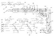
- FIG. 1is a simplified block diagram of an OFDM transmitter PMD
- FIG. 2is a diagram of an OFDM PPDU frame.
- FIG. 3is a simplified block diagram of an OFDM receiver PMD.
- FIG. 4Calculation flow diagram for improved compensation for common phase error and sampling phase drift.
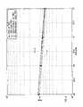
- FIG. 5is a plot of simulation results at 24 Mbps.
- FIG. 6is a plot of simulation results at 54 Mbps.
- FIG. 7is a plot of simulation results at 72 Mbps.
- FIG. 8is a plot of simulation results at 72 Mbps with 2 degrees rms phase noise.
- FIG. 9is a simplified block diagram of a transceiver incorporating the transmitter of FIG. 1 and the receiver of FIG. 3 .
- FIG. 1is a simplified block diagram of an OFDM transmitter PMD compliant with the IEEE 802.11a standard. This illustrates generally a representative environment or application in connection with which the present invention can be used.
- an outbound PPDUi.e. a data unit
- This data unitdescribed in greater detail below, has a preamble, a header, data portion, tail, pad bits etc.
- the bit streamis input to a convolutional encoder 102 .
- bit interleaving and mapping block 104Bit interleaving is accomplished by a block interleaver with a block size corresponding to the number of bits in a single OFDM symbol, N CBPS , as detailed in the 802.11a standard at 17.3.5.6.
- the first permutationensures that adjacent coded bits are mapped onto nonadjacent sub-carriers.
- the second permutation stepensures that adjacent coded bits are mapped alternately onto less and more significant bits of the constellation and, thereby, long runs of low reliability (LSB) bits are avoided.
- LSBlow reliability
- Block 104 in FIG. 1also represents mapping the data, in other words symbol modulation.
- the encoded and interleaved binary serial input datais divided into groups of bits, each group sized according to the selected modulation (1, 2, 4 or 6 bits). For example, 64-QAM modulation maps 6-bit quantities onto the constellation.
- 64-QAM modulationmaps 6-bit quantities onto the constellation.
- the same procedurescan be extended to higher rate encoding, e.g. 256-QAM, in which case each group of 8 bits of the serial data is mapped onto one complex number (I+jQ) corresponding to a location on the 256-QAM constellation.
- the output valuesare multiplied by a normalization factor, depending on the base modulation mode (for 64-QAM, it is 1/ ⁇ square root over (4) ⁇ ) to achieve the same average power for all mappings.
- the symbol durationis 4.0 ⁇ sec.
- Each group of 48 numbersis mapped to a corresponding one of 48 useful sub-carriers, frequency offset index numbers ⁇ 26 to +26. Accordingly each sub-carrier (except the pilot sub-carriers) will be modulated by one complex number for each OFDM symbol in the current data unit.
- pilot signalsare put in sub-carriers ⁇ 21, ⁇ 7, 7 and 21 according to the industry standard.
- the pilotsare BPSK modulated by a pseudo binary sequence to prevent the generation of spectral lines.
- the inverse FFT 106receives all 52 sub-carrier signals and combines them to form a time domain digital signal. Next, a guard interval (not shown) is inserted.
- the guard intervalis to increase immunity to multipath by extending the length of the transmitted symbol. (It is also known as CP or cyclic prefix.)
- the window length used in the demodulator in the receiver to decode the symbolis that of the active symbol length, in other words excluding the guard interval period.
- Symbol wave shapingfollows, block 108 , and then modulation onto I and Q phase quadrature carriers at 110 , and finally the combined signal is modulated onto the radio frequency carrier fc for transmission from antenna 112 .
- the transmitted time-domain signal(after D/A conversion at rate 1/T) is represented by
- X kare the frequency-domain data symbols.
- the N values X krepresent the respective values of the discretely-varying (e.g. QPSK or QAM) signals modulating the OFDM carriers.
- FIG. 2is a block diagram illustrating the structure of a PLCP protocol data unit (PPDU) frame, in accordance with the IEEE 802.11a standard.
- this frame structureis a part of the IEEE 802.11a physical layer extension to the basic 802.11 protocol.
- the 802.11a extensiondefines requirements for a PHY operating in the 5.0 GHz unlicensed frequency bands and data rates ranging from 6 Mbps to 54 Mbps.
- the PPDU (PLCP protocol data unit) frameconsists of a PLCP preamble and signal and data fields as illustrated in FIG. 2 .
- the receiveruses the PLCP preamble to acquire the incoming OFDM signal and synchronize the demodulator.
- the PLCP headercontains information about the PSDU (PLCP service data unit) or payload from the sending OFDM PHY.
- the PLCP preamble 202is used to acquire the incoming signal and train and synchronize the receiver.
- the PLCP preambleconsists of 12 symbols, 10 of which are short symbols, and 2 long symbols.
- the short symbolsare used to train the receiver's AGC and obtain a course estimate of the carrier frequency and the channel.
- the long symbolsare used to fine-tune the frequency and channel estimates. Twelve sub-carriers are used for the short symbols and 53 for the long.
- the training of an OFDMis accomplished in 16 microseconds. This is calculated as 10 short symbols times 0.8 microseconds each, plus 2 long training symbols at 3.2 microseconds each, plus the guard interval. See IEEE standard 802.11a (1999) Section 17.3.3. These training symbols, as noted above, provide for a channel and frequency offset estimation, but do not compensate for other factors such as sampling frequency jitter.
- the preamble field 202is followed by a signal field 204 which consists of one OFDM symbol.
- Thiscontains the rate and length fields as requested by the MAC.
- the rate fieldconveys information about the type of modulation and the coding rate as used in the rest of the packet.
- the SIGNAL fieldis composed of 24 bits, with bits 0 to 3 encoding the rate, bit 4 reserved, and bits 5 - 16 encoding the length of the packet, with the LSB being transmitted first.
- a single parity bit and 6-bit tail fieldcomplete the SIGNAL symbol.
- the SIGNAL field 204is followed by the data 206 comprising a variable number of OFDM symbols including the SERVICE field still forming part of the PLCP Header, consistent with the length specified in the SIGNAL field 204 .
- the receiverincludes a low-noise amplifier 120 , IF detector 122 driver by a local oscillator, and automatic gain control circuit (AGC) 124 as are well known.
- the resulting signalis input to an IQ detector 130 to recover I and Q phase quadrature analog signals, which are used by AFC clock recover 132 to adjust local oscillator 134 to synchronize with received signals.
- the recovered signalsare converted to digital data by A/D sampling (not shown), guard interval removed 136 , and the stream of data is converted to parallel form for input to FFT 140 .
- the FFT(implementation of the Discrete Fourier Transform) demodulates the data from the sub-carrier signals to recover the 52 signals which in turn are serialized and then input to block 142 for bit de-interleaving and de-mapping (from the constellation) back into a serial binary stream, which then undergoes convolutional decoding 144 to recover the inbound data unit PPDU 150 transmitted by an incident OFDM transmitter arranged in accordance with the transmitter 180 shown in FIG. 1 . Further details of this type of receiver are known, but the need remains for improvements in performance especially at higher data rates, i.e. above 54 Mbps which is not currently considered by the IEEE 802.11a (1999) and 802.11g (2002 draft) standards.
- the OFDM systemcan be modeled as follows.
- the transmitted time-domain signal(after D/A conversion at rate 1/T) is represented by e.g. n(1) discussed above,
- X kare the frequency-domain data symbols.
- the N values X krepresent the respective values of the discretely-varying (e.g. QPSK or QAM) signals modulating the OFDM carriers.
- Multipathis a performance concern that also must be taken into account. Multipath occurs when the direct path of the transmitted signal is combined with reflected signal paths, resulting in a corrupted signal at the receiver.
- the delay of the reflected signalsa function of the propagation environment, typically around 50-300 nanoseconds, is commonly known as delay spread.
- We model the transmitted signalas distorted by a multipath channel with impulse response h(t).
- h(t)impulse response
- residual frequency offset and phase noisecontribute to a multiplicative distortion e J ⁇ (t) .
- white Gaussian noise v(t)is added to form the received signal y(t).
- y ( t )e J ⁇ (t) [h ( t )* x ( t )]+ v ( t ) (2)
- the received signalis sampled at the A/D converter (at rate 1/T) with some jitter (represented by sn) on the sampling phase.
- the A/D outputcan be written as
- N n([n+s n ]T)
- v nv([n+s n ]T).
- the DFTDiscrete Fourier Transform
- This compensation methodhas a constant term A to account for residual carrier frequency offset and phase noise, and a second term kB that increases linearly with the sub-carrier index to account for sampling phase offsets.
- Ato account for residual carrier frequency offset and phase noise
- kBthat increases linearly with the sub-carrier index to account for sampling phase offsets.
- the “average” value of the jitter over one OFDM symbolresults in the “sampling phase offset” for which we compensate.
- the next sectiondescribes maximum likelihood estimates for A and B.
- a MLm 22 ⁇ r 1 - m 12 ⁇ r 2 m 11 ⁇ m 22 - m 12 2 ( 8 )
- B ML- m 12 ⁇ r 1 + m 11 ⁇ r 2 m 11 ⁇ m 22 - m 12 2 ⁇ ⁇
- m 11⁇ k ⁇ K ⁇ ⁇ H ⁇ k ⁇ X k ⁇ 2 ( 10 )
- m 12⁇ k ⁇ K ⁇ k ⁇ ⁇ H ⁇ k ⁇ X k ⁇ 2 ( 11 )
- m 22⁇ k ⁇ K ⁇ k 2 ⁇ ⁇ H ⁇ k ⁇ X k ⁇ 2 ( 12 )
- r 1⁇ k ⁇ K ⁇ Y k ⁇ H ⁇ k * ⁇ X k * ( 13 )
- r 2⁇ k ⁇ K ⁇ kY k ⁇ H ⁇
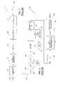
- FIG. 4is a block diagram illustrating calculation of the compensation for updating channel estimates to compensate for carrier phase error and sampling phase offset in accordance with the present invention.
- a shift register 400is formed of a series of delay of individual delay elements, for example, 402 so as form and coder/decoder arranged to remove the known modulation of the pilot carriers.
- Each delay element 402delays the signal by one OFDM symbol.
- the shift registeris initialized to a state of all ones starting from the SIGNAL symbol (see FIG. 2 ). (The term “shift register” is used here to describe the functional arrangement of these elements.
- Element 404translates zeros into ones and ones into minus ones and the resulting signals are input to a series of four multiplier circuits 410 except that one of the signals is multiplied by minus one in multiplier 412 .
- the products produced by 410are the pilot tones with the known BPSK modulation removed (i.e. the multiplications are actually sign changes depending on the shift register output).
- each of these signalsis input to a corresponding multiplier, collectively labeled 418 and multiplied by the complex conjugate of the corresponding channel estimate, for example, H* ⁇ 7 indicated at 420 .
- the details of implementing multipliers, including complex multipliers,are well known.
- the resulting four productsare summed in summation circuit 422 to form the signal r 1 at node 424 .
- Element 404converts the shift register output from bits (0 or 1) to + ⁇ 1 to change the sign of the pilot sub-carrier signals.
- the pilot sub-carrier index numbersare input to a series of multipliers 426 in which each of them is multiplied by the corresponding products of multipliers 418 .
- the outputs (products) of multipliers 426are summed in element 430 to form the quantity r 2 in accordance with the equation 14 above.
- the channel estimates H ⁇ 21 H ⁇ 7 H 7 and H 21are input to a series of elements 440 each of which produces a quantity equal to the square of the magnitude of the corresponding input signal.
- Each channel estimateis, of course, a complex number, indicating the channel frequency and nominal phase.
- These quantitiesare summed in element 442 to provide m 11 in accordance with equation 10 above.
- 2are each multiplied by the corresponding sub-carrier index in multipliers 446 , respectively, and then summed in element 448 to form the quantity m 12 , as reflected in equation 11 above.
- multipliers 446are again multiplied by the corresponding sub-carrier indexes in multipliers 450 , and the resulting products are summed in element 452 so as to form the quantity m 22 in accordance with equation 12 above.
- FIG. 4merely illustrates certain calculations; it is not a hardware schematic.
- the illustrated calculationscan be implemented in hardware, e.g. a DSP or microprocessor core, with appropriate software, or dedicated custom hardware could be used, in whole or in part.
- Various arrangementscan be devised by those of ordinary skill in view of the present disclosure without departing from the scope of the present invention.
- FIG. 5is a plot of the packet-error rate (PER) versus signal-to-noise ratio (SNR) for the 24 Mbps mode and 50-ns rms delay spread multipath channels.
- the rms phase noiseis set to 3° with a 3-dB frequency of 20 kHz.
- the in-phase/quadrature imbalanceis set to 1° and 1% gain imbalance.
- the “no TBG” curvesshow the simulation results when no sampling jitter was present; the “50 ps TBG” curves (labeled X and Z) in FIGS.
- FIG. 6plots simulation results at 54 Mbps mode and 25-ns rms delay spread.
- the performance for “CPE” and “affine” methodsare nearly identical in the presence of the TBG jitter (curves X and Z respectively). In other words, little performance benefit is realized under these conditions.
- FIG. 7plots simulation results for the 72 Mbps mode using 256 QAM and a rate 3/4 convolutional code. From the plot, there is a loss of around 2.7 dB at 10% PER using the “affine” compensation method (curve Y) compared to the “CPE” method (curve W) when no jitter is present. As mentioned earlier, this loss is caused by estimated two parameters (A and B) using the 4 pilot tones, when in fact one parameter (A) is sufficient when no jitter is present. However, when TBG jitter is included, the “affine” compensation method (curve Z) performs significantly better than the “CPE” method (curve X).
- the loss of the “affine” compensation method (curve Y) with respect to the “CPE” method (curve W)is around 1.2 dB at 10% PER when no jitter is present.
- the “affine” method (curve Z)has a gain of around 3.1 dB at 10% PER compared to the “CPE” method (curve X).
- the present inventionis particularly advantageous at 72 Mbps, and in general appears to be useful at data rates over 54 Mbps.
- Implementation of a receiver that embodies the inventionrequires additional circuitry (consistent with the flow diagram illustrated in FIG. 4 ) as compared to a conventional receiver design, with an attendant increase in power consumption.
- the inventionsince the invention is most useful at higher data rates, e.g. over 54 Mbps, it could be implemented with an enable or switching circuit so that the extra circuitry to implement the above compensation of channel estimates could be turned on only when needed, thereby saving power consumption during operation at lower data rates.
- FIG. 9shows a transceiver 900 capable of implementing the teachings of the present invention, and includes receiver 300 described above with reference to FIG. 3 and a transmitter 180 described above with reference to FIG. 1 communicatively coupled to a network interface such as a MAC interface 910 .
- a network interfacesuch as a MAC interface 910 .
- inbound PPDUe.g. PPDU 150 in FIG. 3
- outbound PPDUe.g. PPDU 100 in FIG. 1
- the MAC I/F 910is relayed by the MAC I/F 910 to the transmitter 180 for transmission over a wireless medium such as air via the antenna 112 .
- a wireless mediumsuch as air via the antenna 112 .
- the transceiver 900may form an operational part of a network interface apparatus such as a PC card or network interface card capable of interfacing with the CPU or information processor of an information processing apparatus such as a desktop or laptop computer, and may be integrated within and constitute a part of such information processing apparatus.
- This network interface apparatusmay alternatively form an operational component of a wireless communications access point such as a base station as will be appreciated by these ordinarily skilled in the art.
Landscapes
- Engineering & Computer Science (AREA)
- Computer Networks & Wireless Communication (AREA)
- Signal Processing (AREA)
- Environmental & Geological Engineering (AREA)
- Digital Transmission Methods That Use Modulated Carrier Waves (AREA)
- Cable Transmission Systems, Equalization Of Radio And Reduction Of Echo (AREA)
- Mobile Radio Communication Systems (AREA)
Abstract
Description
{tilde over (H)}k=(A+kB)Ĥk
where Xkare the frequency-domain data symbols. In other words, the N values Xkrepresent the respective values of the discretely-varying (e.g. QPSK or QAM) signals modulating the OFDM carriers.
y(t)=eJφ(t)[h(t)*x(t)]+v(t) (2)
where Nn=([n+sn]T) and vn=v([n+sn]T). After simplification, we have
where Vkis the DFT of vnand Wkrepresents the intercarrier interference (ICI) and AWGN. If |φn+2πksn/N|<<1,
{tilde over (H)}k=(A+kB)Ĥk (7)
where A and B are complex numbers. This compensation method has a constant term A to account for residual carrier frequency offset and phase noise, and a second term kB that increases linearly with the sub-carrier index to account for sampling phase offsets. The “average” value of the jitter over one OFDM symbol results in the “sampling phase offset” for which we compensate. The next section describes maximum likelihood estimates for A and B.
Maximum Likelihood Compensation of Channel Estimates
The channel estimates are then compensated according to (7) before further processing.
{tilde over (H)}k=AĤk
The “no TBG” curves (labeled W and Y in
Claims (56)
{tilde over (H)}k=(A+kB)Ĥk
{tilde over (H)}k=(A+kB)Ĥk
{tilde over (H)}k=(A+kB)Ĥk.
{tilde over (H)}k=(A+kB)Ĥk
{tilde over (H)}k=(A+kB)Ĥk.
{tilde over (H)}k=(A+kB)Ĥk
{tilde over (H)}k=(A+kB)Ĥk
{tilde over (H)}k=(A+kB)Ĥk
Priority Applications (6)
| Application Number | Priority Date | Filing Date | Title |
|---|---|---|---|
| US10/193,439US7346135B1 (en) | 2002-02-13 | 2002-07-10 | Compensation for residual frequency offset, phase noise and sampling phase offset in wireless networks |
| US12/070,375US7616719B1 (en) | 2002-02-13 | 2008-02-15 | Compensation for residual frequency offset, phase noise and sampling phase offset in wireless networks |
| US12/615,605US8223893B1 (en) | 2002-02-13 | 2009-11-10 | Compensation for residual frequency offset, phase noise and sampling phase offset in wireless networks |
| US13/548,883US8767879B1 (en) | 2002-02-13 | 2012-07-13 | Compensation for residual frequency offset, phase noise and sampling phase offset in wireless networks |
| US14/314,684US9185013B1 (en) | 2002-02-13 | 2014-06-25 | Systems and methods for compensating a channel estimate for sampling phase jitter |
| US14/927,982US9432276B1 (en) | 2002-02-13 | 2015-10-30 | Systems and methods for compensating a channel estimate for phase and sampling phase jitter |
Applications Claiming Priority (2)
| Application Number | Priority Date | Filing Date | Title |
|---|---|---|---|
| US35647502P | 2002-02-13 | 2002-02-13 | |
| US10/193,439US7346135B1 (en) | 2002-02-13 | 2002-07-10 | Compensation for residual frequency offset, phase noise and sampling phase offset in wireless networks |
Related Child Applications (1)
| Application Number | Title | Priority Date | Filing Date |
|---|---|---|---|
| US12/070,375ContinuationUS7616719B1 (en) | 2002-02-13 | 2008-02-15 | Compensation for residual frequency offset, phase noise and sampling phase offset in wireless networks |
Publications (1)
| Publication Number | Publication Date |
|---|---|
| US7346135B1true US7346135B1 (en) | 2008-03-18 |
Family
ID=39182268
Family Applications (6)
| Application Number | Title | Priority Date | Filing Date |
|---|---|---|---|
| US10/193,439Expired - LifetimeUS7346135B1 (en) | 2002-02-13 | 2002-07-10 | Compensation for residual frequency offset, phase noise and sampling phase offset in wireless networks |
| US12/070,375Expired - LifetimeUS7616719B1 (en) | 2002-02-13 | 2008-02-15 | Compensation for residual frequency offset, phase noise and sampling phase offset in wireless networks |
| US12/615,605Expired - Fee RelatedUS8223893B1 (en) | 2002-02-13 | 2009-11-10 | Compensation for residual frequency offset, phase noise and sampling phase offset in wireless networks |
| US13/548,883Expired - LifetimeUS8767879B1 (en) | 2002-02-13 | 2012-07-13 | Compensation for residual frequency offset, phase noise and sampling phase offset in wireless networks |
| US14/314,684Expired - Fee RelatedUS9185013B1 (en) | 2002-02-13 | 2014-06-25 | Systems and methods for compensating a channel estimate for sampling phase jitter |
| US14/927,982Expired - Fee RelatedUS9432276B1 (en) | 2002-02-13 | 2015-10-30 | Systems and methods for compensating a channel estimate for phase and sampling phase jitter |
Family Applications After (5)
| Application Number | Title | Priority Date | Filing Date |
|---|---|---|---|
| US12/070,375Expired - LifetimeUS7616719B1 (en) | 2002-02-13 | 2008-02-15 | Compensation for residual frequency offset, phase noise and sampling phase offset in wireless networks |
| US12/615,605Expired - Fee RelatedUS8223893B1 (en) | 2002-02-13 | 2009-11-10 | Compensation for residual frequency offset, phase noise and sampling phase offset in wireless networks |
| US13/548,883Expired - LifetimeUS8767879B1 (en) | 2002-02-13 | 2012-07-13 | Compensation for residual frequency offset, phase noise and sampling phase offset in wireless networks |
| US14/314,684Expired - Fee RelatedUS9185013B1 (en) | 2002-02-13 | 2014-06-25 | Systems and methods for compensating a channel estimate for sampling phase jitter |
| US14/927,982Expired - Fee RelatedUS9432276B1 (en) | 2002-02-13 | 2015-10-30 | Systems and methods for compensating a channel estimate for phase and sampling phase jitter |
Country Status (1)
| Country | Link |
|---|---|
| US (6) | US7346135B1 (en) |
Cited By (15)
| Publication number | Priority date | Publication date | Assignee | Title |
|---|---|---|---|---|
| US20050078598A1 (en)* | 2003-08-21 | 2005-04-14 | Anuj Batra | Enhancement to the multi-band OFDM physical layer |
| US20060036924A1 (en)* | 2004-08-16 | 2006-02-16 | Monisha Ghosh | Interleaving and parsing for MIMO-OFDM systems |
| US20060285603A1 (en)* | 2005-06-20 | 2006-12-21 | Samsung Electronics Co., Ltd. | Method and apparatus for performing channel compensation and symbol demodulation for coherent demodulation in an OFDM system |
| US20070058734A1 (en)* | 2005-09-13 | 2007-03-15 | Via Technologies Inc. | Circuit for improving channel impulse response estimation and compensating for remnant frequency offset in the orthogonal frequency division multiplexing baseband receiver for IEEE 802.11a/g wireless LAN standard standard |
| US20070140104A1 (en)* | 2005-09-14 | 2007-06-21 | Samsung Electronics Co., Ltd. | System and method for timing acquisition and carrier frequency offset estimation in wireless communication based on OFDM |
| US20080063101A1 (en)* | 1999-05-14 | 2008-03-13 | Cimini Leonard J Jr | Method for estimating time and frequency offset in an OFDM system |
| US20110116562A1 (en)* | 2009-11-18 | 2011-05-19 | Wi-Lan, Inc. | Digital Communications Receiver and Method of Estimating Residual Carrier Frequency Offset In A Received Signal |
| US20120051287A1 (en)* | 2010-08-31 | 2012-03-01 | Qualcomm Incorporated | Implicit and explicit channel sounding for beamforming |
| US8223893B1 (en) | 2002-02-13 | 2012-07-17 | Marvell International Ltd. | Compensation for residual frequency offset, phase noise and sampling phase offset in wireless networks |
| CN105847198A (en)* | 2016-03-15 | 2016-08-10 | 东南大学 | IQ imbalance estimation and compensation method of OFDM-WLAN radio frequency testing system |
| CN106160882A (en)* | 2016-07-13 | 2016-11-23 | 北京交通大学 | A kind of multiband wireless channel measurement calibration steps and system |
| CN108901070A (en)* | 2018-06-12 | 2018-11-27 | Oppo广东移动通信有限公司 | Wireless communication transmission method, device, mobile terminal and computer-readable storage medium |
| CN109075950A (en)* | 2016-05-09 | 2018-12-21 | 英特尔Ip公司 | Phase compensation reference signal for 5G system |
| CN110730055A (en)* | 2019-10-22 | 2020-01-24 | 上海创远仪器技术股份有限公司 | Method for realizing 5G signal emission modulation quality measurement based on signal analyzer |
| CN112929317A (en)* | 2021-02-05 | 2021-06-08 | Oppo广东移动通信有限公司 | Phase noise estimation method and device, communication device and communication equipment |
Families Citing this family (10)
| Publication number | Priority date | Publication date | Assignee | Title |
|---|---|---|---|---|
| US8139661B2 (en)* | 2005-12-08 | 2012-03-20 | Electronics And Telecommunications Research Institute | Signal transmitting and receiving apparatuses |
| US8035537B2 (en)* | 2008-06-13 | 2011-10-11 | Lsi Corporation | Methods and apparatus for programmable decoding of a plurality of code types |
| KR101791987B1 (en)* | 2010-12-07 | 2017-11-20 | 한국전자통신연구원 | Method and apparatus for transmitting preamble in wireless communication system |
| CN102594740B (en)* | 2011-01-11 | 2015-04-01 | 中兴通讯股份有限公司 | Method and device for estimating frequency offset |
| US8837611B2 (en)* | 2011-02-09 | 2014-09-16 | Silicon Laboratories Inc. | Memory-aided synchronization in a receiver |
| US8848841B2 (en) | 2012-12-27 | 2014-09-30 | Intel Corporation | Techniques to accommodate different classes of devices in a wireless network |
| KR102130658B1 (en)* | 2013-07-26 | 2020-07-06 | 삼성전자주식회사 | Transmitter, receiver and controlling method thereof |
| CN103873416B (en)* | 2014-03-12 | 2017-02-08 | 南京软仪测试技术有限公司 | EVM (Error Vector Magnitude) phase estimating and compensating method |
| CN107404451B (en)* | 2016-05-18 | 2020-05-29 | 上海复旦微电子集团股份有限公司 | BPSK demodulation method and device and receiver |
| CN113497775B (en)* | 2021-09-07 | 2021-12-03 | 南京沁恒微电子股份有限公司 | High-sensitivity receiving method in coded mode of Bluetooth receiver |
Citations (16)
| Publication number | Priority date | Publication date | Assignee | Title |
|---|---|---|---|---|
| US5345440A (en) | 1990-09-14 | 1994-09-06 | National Transcommunications Limited | Reception of orthogonal frequency division multiplexed signals |
| US5450456A (en) | 1993-11-12 | 1995-09-12 | Daimler Benz Ag | Method and arrangement for measuring the carrier frequency deviation in a multi-channel transmission system |
| US5608764A (en) | 1993-11-12 | 1997-03-04 | Kabushiki Kaisha Toshiba | OFDM synchronization demodulation circuit |
| US5640431A (en) | 1995-03-10 | 1997-06-17 | Motorola, Inc. | Method and apparatus for offset frequency estimation for a coherent receiver |
| US5732113A (en) | 1996-06-20 | 1998-03-24 | Stanford University | Timing and frequency synchronization of OFDM signals |
| US5732339A (en) | 1994-10-25 | 1998-03-24 | Alcatel Mobile Commuication France | Frequency offset correction |
| US5838734A (en)* | 1993-05-05 | 1998-11-17 | British Broadcasting Corporation | Compensation for local oscillator errors in an OFDM receiver |
| US5889759A (en) | 1996-08-12 | 1999-03-30 | Telecommunications Research Laboratories | OFDM timing and frequency recovery system |
| US6035003A (en) | 1996-11-29 | 2000-03-07 | Daewoo Electronics Co., Ltd. | Apparatus for correcting frequency offset in OFDM receiving system |
| US6198782B1 (en) | 1999-02-11 | 2001-03-06 | Motorola, Inc. | Estimation of frequency offsets in OFDM communication systems |
| US20010031022A1 (en) | 1996-10-11 | 2001-10-18 | Paul Petrus | Method for reference signal generation in the presence of frequency offsets in a communications station with spatial processing |
| EP1160981A2 (en) | 2000-05-30 | 2001-12-05 | Nokia Mobile Phones Ltd. | Method and arrangement for reducing frequency offset in a radio receiver |
| US20020065047A1 (en)* | 2000-11-30 | 2002-05-30 | Moose Paul H. | Synchronization, channel estimation and pilot tone tracking system |
| US20020085651A1 (en)* | 2000-10-16 | 2002-07-04 | Jian Gu | Removing frequency and timing offsets in digital transmitters and receivers |
| US20020101840A1 (en)* | 2000-11-29 | 2002-08-01 | Stefan Davidsson | Timing drift compensation in wireless packet-based systems |
| US6658063B1 (en)* | 1999-07-19 | 2003-12-02 | Nippon Telegraph And Telephone Corporation | OFDM packet communication receiver system |
Family Cites Families (275)
| Publication number | Priority date | Publication date | Assignee | Title |
|---|---|---|---|---|
| US1355846A (en) | 1920-02-06 | 1920-10-19 | David A Rannells | Medical appliance |
| US2547758A (en) | 1949-01-05 | 1951-04-03 | Wilmer B Keeling | Instrument for treating the male urethra |
| US2632443A (en) | 1949-04-18 | 1953-03-24 | Eleanor P Lesher | Surgical dressing |
| US2682873A (en) | 1952-07-30 | 1954-07-06 | Johnson & Johnson | General purpose protective dressing |
| NL189176B (en) | 1956-07-13 | 1900-01-01 | Hisamitsu Pharmaceutical Co | PLASTER BASED ON A SYNTHETIC RUBBER. |
| US2969057A (en) | 1957-11-04 | 1961-01-24 | Brady Co W H | Nematodic swab |
| US3066672A (en) | 1960-09-27 | 1962-12-04 | Jr William H Crosby | Method and apparatus for serial sampling of intestinal juice |
| US3367332A (en) | 1965-08-27 | 1968-02-06 | Gen Electric | Product and process for establishing a sterile area of skin |
| US3520300A (en) | 1967-03-15 | 1970-07-14 | Amp Inc | Surgical sponge and suction device |
| US3568675A (en) | 1968-08-30 | 1971-03-09 | Clyde B Harvey | Fistula and penetrating wound dressing |
| US3682180A (en) | 1970-06-08 | 1972-08-08 | Coilform Co Inc | Drain clip for surgical drain |
| BE789293Q (en) | 1970-12-07 | 1973-01-15 | Parke Davis & Co | MEDICO-SURGICAL DRESSING FOR BURNS AND SIMILAR LESIONS |
| US3826254A (en) | 1973-02-26 | 1974-07-30 | Verco Ind | Needle or catheter retaining appliance |
| DE2527706A1 (en) | 1975-06-21 | 1976-12-30 | Hanfried Dr Med Weigand | DEVICE FOR THE INTRODUCTION OF CONTRAST AGENTS INTO AN ARTIFICIAL INTESTINAL OUTLET |
| NL7710909A (en) | 1976-10-08 | 1978-04-11 | Smith & Nephew | COMPOSITE STRAPS. |
| GB1562244A (en) | 1976-11-11 | 1980-03-05 | Lock P M | Wound dressing materials |
| US4080970A (en) | 1976-11-17 | 1978-03-28 | Miller Thomas J | Post-operative combination dressing and internal drain tube with external shield and tube connector |
| US4139004A (en) | 1977-02-17 | 1979-02-13 | Gonzalez Jr Harry | Bandage apparatus for treating burns |
| US4184510A (en) | 1977-03-15 | 1980-01-22 | Fibra-Sonics, Inc. | Valued device for controlling vacuum in surgery |
| US4165748A (en) | 1977-11-07 | 1979-08-28 | Johnson Melissa C | Catheter tube holder |
| US4245637A (en) | 1978-07-10 | 1981-01-20 | Nichols Robert L | Shutoff valve sleeve |
| SE414994B (en) | 1978-11-28 | 1980-09-01 | Landstingens Inkopscentral | VENKATETERFORBAND |
| GB2047543B (en) | 1978-12-06 | 1983-04-20 | Svedman Paul | Device for treating tissues for example skin |
| US4284079A (en) | 1979-06-28 | 1981-08-18 | Adair Edwin Lloyd | Method for applying a male incontinence device |
| US4261363A (en) | 1979-11-09 | 1981-04-14 | C. R. Bard, Inc. | Retention clips for body fluid drains |
| US4569348A (en) | 1980-02-22 | 1986-02-11 | Velcro Usa Inc. | Catheter tube holder strap |
| WO1981002516A1 (en) | 1980-03-11 | 1981-09-17 | E Schmid | Cushion for holding an element of grafted skin |
| US4297995A (en) | 1980-06-03 | 1981-11-03 | Key Pharmaceuticals, Inc. | Bandage containing attachment post |
| US4456965A (en) | 1980-10-14 | 1984-06-26 | Texas Instruments Incorporated | Data processing system having multiple buses |
| US4465485A (en) | 1981-03-06 | 1984-08-14 | Becton, Dickinson And Company | Suction canister with unitary shut-off valve and filter features |
| US4392853A (en) | 1981-03-16 | 1983-07-12 | Rudolph Muto | Sterile assembly for protecting and fastening an indwelling device |
| US4373519A (en) | 1981-06-26 | 1983-02-15 | Minnesota Mining And Manufacturing Company | Composite wound dressing |
| US4392858A (en) | 1981-07-16 | 1983-07-12 | Sherwood Medical Company | Wound drainage device |
| US4419097A (en) | 1981-07-31 | 1983-12-06 | Rexar Industries, Inc. | Attachment for catheter tube |
| SE429197B (en) | 1981-10-14 | 1983-08-22 | Frese Nielsen | SAR TREATMENT DEVICE |
| DE3146266A1 (en) | 1981-11-21 | 1983-06-01 | B. Braun Melsungen Ag, 3508 Melsungen | COMBINED DEVICE FOR A MEDICAL SUCTION DRAINAGE |
| US4551139A (en) | 1982-02-08 | 1985-11-05 | Marion Laboratories, Inc. | Method and apparatus for burn wound treatment |
| US4475909A (en) | 1982-05-06 | 1984-10-09 | Eisenberg Melvin I | Male urinary device and method for applying the device |
| US4548202A (en) | 1983-06-20 | 1985-10-22 | Ethicon, Inc. | Mesh tissue fasteners |
| US4540412A (en) | 1983-07-14 | 1985-09-10 | The Kendall Company | Device for moist heat therapy |
| US4543100A (en) | 1983-11-01 | 1985-09-24 | Brodsky Stuart A | Catheter and drain tube retainer |
| US4525374A (en) | 1984-02-27 | 1985-06-25 | Manresa, Inc. | Treating hydrophobic filters to render them hydrophilic |
| US4897081A (en) | 1984-05-25 | 1990-01-30 | Thermedics Inc. | Percutaneous access device |
| US5215522A (en) | 1984-07-23 | 1993-06-01 | Ballard Medical Products | Single use medical aspirating device and method |
| GB8419745D0 (en) | 1984-08-02 | 1984-09-05 | Smith & Nephew Ass | Wound dressing |
| US4872450A (en) | 1984-08-17 | 1989-10-10 | Austad Eric D | Wound dressing and method of forming same |
| US4655754A (en) | 1984-11-09 | 1987-04-07 | Stryker Corporation | Vacuum wound drainage system and lipids baffle therefor |
| US4826494A (en) | 1984-11-09 | 1989-05-02 | Stryker Corporation | Vacuum wound drainage system |
| US4605399A (en) | 1984-12-04 | 1986-08-12 | Complex, Inc. | Transdermal infusion device |
| US5037397A (en) | 1985-05-03 | 1991-08-06 | Medical Distributors, Inc. | Universal clamp |
| US4640688A (en) | 1985-08-23 | 1987-02-03 | Mentor Corporation | Urine collection catheter |
| US4710165A (en) | 1985-09-16 | 1987-12-01 | Mcneil Charles B | Wearable, variable rate suction/collection device |
| US4758220A (en) | 1985-09-26 | 1988-07-19 | Alcon Laboratories, Inc. | Surgical cassette proximity sensing and latching apparatus |
| US4747047A (en) | 1985-12-06 | 1988-05-24 | Unisys Corporation | Data transfer system using two peripheral controllers to access dual-ported data storage units |
| US4733659A (en) | 1986-01-17 | 1988-03-29 | Seton Company | Foam bandage |
| US4838883A (en) | 1986-03-07 | 1989-06-13 | Nissho Corporation | Urine-collecting device |
| JPS62281965A (en) | 1986-05-29 | 1987-12-07 | テルモ株式会社 | Catheter and catheter fixing member |
| GB8621884D0 (en) | 1986-09-11 | 1986-10-15 | Bard Ltd | Catheter applicator |
| US4743232A (en) | 1986-10-06 | 1988-05-10 | The Clinipad Corporation | Package assembly for plastic film bandage |
| DE3634569A1 (en) | 1986-10-10 | 1988-04-21 | Sachse Hans E | CONDOM CATHETER, A URINE TUBE CATHETER FOR PREVENTING RISING INFECTIONS |
| JPS63135179A (en) | 1986-11-26 | 1988-06-07 | 立花 俊郎 | Subcataneous drug administration set |
| GB8706116D0 (en) | 1987-03-14 | 1987-04-15 | Smith & Nephew Ass | Adhesive dressings |
| US4787888A (en) | 1987-06-01 | 1988-11-29 | University Of Connecticut | Disposable piezoelectric polymer bandage for percutaneous delivery of drugs and method for such percutaneous delivery (a) |
| US4863449A (en) | 1987-07-06 | 1989-09-05 | Hollister Incorporated | Adhesive-lined elastic condom cathether |
| US5176663A (en) | 1987-12-02 | 1993-01-05 | Pal Svedman | Dressing having pad with compressibility limiting elements |
| US4906240A (en) | 1988-02-01 | 1990-03-06 | Matrix Medica, Inc. | Adhesive-faced porous absorbent sheet and method of making same |
| US4985019A (en) | 1988-03-11 | 1991-01-15 | Michelson Gary K | X-ray marker |
| US4919654A (en) | 1988-08-03 | 1990-04-24 | Kalt Medical Corporation | IV clamp with membrane |
| US5023624A (en) | 1988-10-26 | 1991-06-11 | Harris Corporation | Microwave chip carrier package having cover-mounted antenna element |
| US5059596A (en) | 1989-01-16 | 1991-10-22 | Roussel Uclaf | Azabicyclo compounds |
| US4969880A (en) | 1989-04-03 | 1990-11-13 | Zamierowski David S | Wound dressing and treatment method |
| US5261893A (en) | 1989-04-03 | 1993-11-16 | Zamierowski David S | Fastening system and method |
| US5527293A (en) | 1989-04-03 | 1996-06-18 | Kinetic Concepts, Inc. | Fastening system and method |
| US5100396A (en) | 1989-04-03 | 1992-03-31 | Zamierowski David S | Fluidic connection system and method |
| US5210855A (en) | 1989-06-09 | 1993-05-11 | International Business Machines Corporation | System for computer peripheral bus for allowing hot extraction on insertion without disrupting adjacent devices |
| JP2719671B2 (en) | 1989-07-11 | 1998-02-25 | 日本ゼオン株式会社 | Wound dressing |
| US5358494A (en) | 1989-07-11 | 1994-10-25 | Svedman Paul | Irrigation dressing |
| US5232453A (en) | 1989-07-14 | 1993-08-03 | E. R. Squibb & Sons, Inc. | Catheter holder |
| US5134994A (en) | 1990-02-12 | 1992-08-04 | Say Sam L | Field aspirator in a soft pack with externally mounted container |
| US5092858A (en) | 1990-03-20 | 1992-03-03 | Becton, Dickinson And Company | Liquid gelling agent distributor device |
| US5274665A (en) | 1990-12-14 | 1993-12-28 | Interdigital Technology Corporation | Polyopoly overlapping spread spectrum communication system and method |
| US5149331A (en) | 1991-05-03 | 1992-09-22 | Ariel Ferdman | Method and device for wound closure |
| US5245611A (en)* | 1991-05-31 | 1993-09-14 | Motorola, Inc. | Method and apparatus for providing carrier frequency offset compensation in a tdma communication system |
| US5220275A (en) | 1991-07-26 | 1993-06-15 | Ericsson Ge Mobile Communication Holding, Inc. | Accumulator phase digitizer |
| US5283811A (en)* | 1991-09-03 | 1994-02-01 | General Electric Company | Decision feedback equalization for digital cellular radio |
| US5222062A (en) | 1991-10-03 | 1993-06-22 | Compaq Computer Corporation | Expandable communication system with automatic data concentrator detection |
| US5278100A (en) | 1991-11-08 | 1994-01-11 | Micron Technology, Inc. | Chemical vapor deposition technique for depositing titanium silicide on semiconductor wafers |
| US5645081A (en) | 1991-11-14 | 1997-07-08 | Wake Forest University | Method of treating tissue damage and apparatus for same |
| US5636643A (en) | 1991-11-14 | 1997-06-10 | Wake Forest University | Wound treatment employing reduced pressure |
| JPH05165762A (en) | 1991-12-13 | 1993-07-02 | Toshiba Corp | Dma controller |
| US5530960A (en) | 1991-12-17 | 1996-06-25 | Dell Usa, L.P. | Disk drive controller accepting first commands for accessing composite drives and second commands for individual diagnostic drive control wherein commands are transparent to each other |
| US5279550A (en) | 1991-12-19 | 1994-01-18 | Gish Biomedical, Inc. | Orthopedic autotransfusion system |
| US5167613A (en) | 1992-03-23 | 1992-12-01 | The Kendall Company | Composite vented wound dressing |
| EP0567033B1 (en) | 1992-04-23 | 1997-12-10 | Hitachi, Ltd. | Frequency synthesizer |
| FR2690617B1 (en) | 1992-04-29 | 1994-06-24 | Cbh Textile | TRANSPARENT ADHESIVE DRESSING. |
| US5331646A (en) | 1992-05-08 | 1994-07-19 | Compaq Computer Corporation | Error correcting code technique for improving reliablility of a disk array |
| US5471585A (en) | 1992-09-17 | 1995-11-28 | International Business Machines Corp. | Personal computer system with input/output controller having serial/parallel ports and a feedback line indicating readiness of the ports |
| US5342376A (en) | 1993-05-03 | 1994-08-30 | Dermagraphics, Inc. | Inserting device for a barbed tissue connector |
| US6241747B1 (en) | 1993-05-03 | 2001-06-05 | Quill Medical, Inc. | Barbed Bodily tissue connector |
| US5344415A (en) | 1993-06-15 | 1994-09-06 | Deroyal Industries, Inc. | Sterile system for dressing vascular access site |
| US5437651A (en) | 1993-09-01 | 1995-08-01 | Research Medical, Inc. | Medical suction apparatus |
| US5471152A (en) | 1993-10-08 | 1995-11-28 | Crosscheck Technology, Inc. | Storage element for delay testing |
| US5549584A (en) | 1994-02-14 | 1996-08-27 | The Kendall Company | Apparatus for removing fluid from a wound |
| JP2938337B2 (en) | 1994-03-09 | 1999-08-23 | 三菱電機株式会社 | Data demodulation circuit for spread spectrum communication |
| EP0676699B1 (en) | 1994-04-04 | 2001-07-04 | Hyundai Electronics America | Method of managing resources shared by multiple processing units |
| US5556375A (en) | 1994-06-16 | 1996-09-17 | Hercules Incorporated | Wound dressing having a fenestrated base layer |
| US5607388A (en) | 1994-06-16 | 1997-03-04 | Hercules Incorporated | Multi-purpose wound dressing |
| US5664270A (en) | 1994-07-19 | 1997-09-09 | Kinetic Concepts, Inc. | Patient interface system |
| US5564114A (en) | 1995-01-09 | 1996-10-08 | Cirrus Logic Inc. | Method and an arrangement for handshaking on a bus to transfer information between devices in a computer system |
| US5553230A (en) | 1995-01-18 | 1996-09-03 | Hewlett-Packard Company | Identifying controller pairs in a dual controller disk array |
| US5606672A (en) | 1995-01-27 | 1997-02-25 | Intel Corporation | Method and apparatus for multiplexing signals from a bus bridge to an ISA bus interface and an ATA bus interface |
| JP3467888B2 (en) | 1995-02-08 | 2003-11-17 | 三菱電機株式会社 | Receiving device and transmitting / receiving device |
| US6239752B1 (en) | 1995-02-28 | 2001-05-29 | Stmicroelectronics, Inc. | Semiconductor chip package that is also an antenna |
| DE69614291T2 (en) | 1995-03-17 | 2001-12-06 | Lsi Logic Corp., Fort Collins | (n + i) input / output channel control, with (n) data managers, in a homogeneous software programming operating environment |
| US5828696A (en)* | 1995-03-30 | 1998-10-27 | Lucent Technologies Inc. | Timing recovery in a network-synchronized modem |
| US5802318A (en) | 1995-07-25 | 1998-09-01 | Compaq Computer Corporation | Universal serial bus keyboard system |
| JPH0997177A (en) | 1995-09-29 | 1997-04-08 | Toshiba Corp | Computer system interrupt control method |
| US5783960A (en) | 1995-11-28 | 1998-07-21 | International Business Machines Corporation | Integrated circuit device with improved clock signal control |
| JPH09266499A (en) | 1996-01-26 | 1997-10-07 | Oki Electric Ind Co Ltd | Digital demodulating circuit, maximum detecting circuit, and reception device |
| US6018778A (en) | 1996-05-03 | 2000-01-25 | Netcell Corporation | Disk array controller for reading/writing striped data using a single address counter for synchronously transferring data between data ports and buffer memory |
| US6368469B1 (en) | 1996-05-09 | 2002-04-09 | Applied Materials, Inc. | Coils for generating a plasma and for sputtering |
| US5748645A (en) | 1996-05-29 | 1998-05-05 | Motorola, Inc. | Clock scan design from sizzle global clock and method therefor |
| US5854941A (en) | 1996-05-31 | 1998-12-29 | Acceleration Software International Corporation | System for estimating access time by deriving from first and second rotational time from rotational time table based on logical address and head movement time |
| US5949692A (en) | 1996-08-28 | 1999-09-07 | Synopsys, Inc. | Hierarchical scan architecture for design for test applications |
| US5787485A (en) | 1996-09-17 | 1998-07-28 | Marathon Technologies Corporation | Producing a mirrored copy using reference labels |
| US5812754A (en) | 1996-09-18 | 1998-09-22 | Silicon Graphics, Inc. | Raid system with fibre channel arbitrated loop |
| US5870438A (en)* | 1996-09-26 | 1999-02-09 | Rockwell Int'l. Corp. | Fast resynchronization system for high-speed data transmission |
| US5909451A (en) | 1996-11-21 | 1999-06-01 | Sun Microsystems, Inc. | System and method for providing scan chain for digital electronic device having multiple clock domains |
| EP0845738A3 (en) | 1996-11-28 | 2006-09-20 | Hitachi, Ltd. | Storage system which transfers a command and data corresponding to said command subsequent to said command |
| US5886901A (en) | 1997-01-07 | 1999-03-23 | Lsi Logic Corporation | Flip-flop for scan test chain |
| US5826048A (en) | 1997-01-31 | 1998-10-20 | Vlsi Technology, Inc. | PCI bus with reduced number of signals |
| AUPO493597A0 (en) | 1997-02-05 | 1997-02-27 | Liguori, Vincenzo | Logic circuit emulator |
| US6092169A (en) | 1997-04-02 | 2000-07-18 | Compaq Computer Corporation | Apparatus and method for storage subsystem drive movement and volume addition |
| DE69735527D1 (en) | 1997-05-02 | 2006-05-11 | Lsi Logic Corp | Digital method for adaptive clock recovery |
| US6124727A (en) | 1997-07-11 | 2000-09-26 | Adaptec, Inc. | Bias compensator for differential transmission line with voltage bias |
| US6073188A (en) | 1997-07-25 | 2000-06-06 | Compaq Computer Corporation | Electronic switchbox for selection and sharing of internal peripheral devices among different computers, the internal peripheral devices located in slots of a chassis |
| US6135116A (en) | 1997-07-28 | 2000-10-24 | Kci Licensing, Inc. | Therapeutic method for treating ulcers |
| US6021462A (en) | 1997-08-29 | 2000-02-01 | Apple Computer, Inc. | Methods and apparatus for system memory efficient disk access to a raid system using stripe control information |
| GB9719520D0 (en) | 1997-09-12 | 1997-11-19 | Kci Medical Ltd | Surgical drape and suction heads for wound treatment |
| CA2217840C (en) | 1997-10-09 | 2005-05-03 | Northern Telecom Limited | Synchronization system multiple modes of operation |
| US6057863A (en) | 1997-10-31 | 2000-05-02 | Compaq Computer Corporation | Dual purpose apparatus, method and system for accelerated graphics port and fibre channel arbitrated loop interfaces |
| US6134630A (en) | 1997-11-14 | 2000-10-17 | 3Ware | High-performance bus architecture for disk array system |
| GB2334116A (en) | 1998-02-04 | 1999-08-11 | Ibm | Scheduling and dispatching queued client requests within a server computer |
| US6071267A (en) | 1998-02-06 | 2000-06-06 | Kinetic Concepts, Inc. | Medical patient fluid management interface system and method |
| US6201796B1 (en) | 1998-05-14 | 2001-03-13 | Broadcom Corporation | Startup protocol for high throughput communications systems |
| US6223238B1 (en) | 1998-03-31 | 2001-04-24 | Micron Electronics, Inc. | Method of peer-to-peer mastering over a computer bus |
| JP3726484B2 (en) | 1998-04-10 | 2005-12-14 | 株式会社日立製作所 | Storage subsystem |
| EP0969636B1 (en) | 1998-06-30 | 2007-04-25 | Lucent Technologies Inc. | Tracking carrier timing utilising frequency offset error signal |
| US6488643B1 (en) | 1998-10-08 | 2002-12-03 | Kci Licensing, Inc. | Wound healing foot wrap |
| US6330687B1 (en) | 1998-11-13 | 2001-12-11 | Digi-Data Corporation | System and method to maintain performance among N single raid systems during non-fault conditions while sharing multiple storage devices during conditions of a faulty host computer or faulty storage array controller |
| US6363439B1 (en) | 1998-12-07 | 2002-03-26 | Compaq Computer Corporation | System and method for point-to-point serial communication between a system interface device and a bus interface device in a computer system |
| US6367033B1 (en) | 1998-12-11 | 2002-04-02 | Lsi Logic Corporation | Method and apparatus for recreating fiber channel traffic |
| US6662076B1 (en) | 1999-02-10 | 2003-12-09 | Advanced Micro Devices, Inc. | Management of move requests from a factory system to an automated material handling system |
| US6287316B1 (en) | 1999-03-26 | 2001-09-11 | Ethicon, Inc. | Knitted surgical mesh |
| US7799004B2 (en) | 2001-03-05 | 2010-09-21 | Kci Licensing, Inc. | Negative pressure wound treatment apparatus and infection identification system and method |
| US6856821B2 (en) | 2000-05-26 | 2005-02-15 | Kci Licensing, Inc. | System for combined transcutaneous blood gas monitoring and vacuum assisted wound closure |
| US6484294B1 (en) | 1999-04-23 | 2002-11-19 | Hitachi, Ltd. | Semiconductor integrated circuit and method of designing the same |
| US6697885B1 (en) | 1999-05-22 | 2004-02-24 | Anthony E. B. Goodfellow | Automated DMA engine for ATA control |
| US6564271B2 (en) | 1999-06-09 | 2003-05-13 | Qlogic Corporation | Method and apparatus for automatically transferring I/O blocks between a host system and a host adapter |
| JP3867447B2 (en) | 1999-06-22 | 2007-01-10 | ソニー株式会社 | Disc type data recording / reproducing apparatus and information processing system equipped with disc type data recording / reproducing apparatus |
| US6991643B2 (en) | 2000-12-20 | 2006-01-31 | Usgi Medical Inc. | Multi-barbed device for retaining tissue in apposition and methods of use |
| US6704300B1 (en) | 1999-08-16 | 2004-03-09 | Nortel Networks Limited | Method and system for acquisition of a time stamped signal |
| US6480930B1 (en) | 1999-09-15 | 2002-11-12 | Emc Corporation | Mailbox for controlling storage subsystem reconfigurations |
| US6388590B1 (en) | 1999-09-24 | 2002-05-14 | Oak Technology, Inc. | Apparatus and method for transmitting data serially for use with an advanced technology attachment packet interface (atapi) |
| US6388591B1 (en) | 1999-09-24 | 2002-05-14 | Oak Technology, Inc. | Apparatus and method for receiving data serially for use with an advanced technology attachment packet interface (atapi) |
| US6442722B1 (en) | 1999-10-29 | 2002-08-27 | Logicvision, Inc. | Method and apparatus for testing circuits with multiple clocks |
| US6731688B1 (en) | 1999-12-13 | 2004-05-04 | Intel Corporation | Speed signaling for data communications |
| US6557065B1 (en) | 1999-12-20 | 2003-04-29 | Intel Corporation | CPU expandability bus |
| US6768460B2 (en) | 2000-03-29 | 2004-07-27 | Matsushita Electric Industrial Co., Ltd. | Diversity wireless device and wireless terminal unit |
| US7206843B1 (en) | 2000-04-21 | 2007-04-17 | Sun Microsystems, Inc. | Thread-safe portable management interface |
| US6447655B2 (en) | 2000-05-30 | 2002-09-10 | Alexander D. Lantsman | DC plasma power supply for a sputter deposition |
| US6614842B1 (en) | 2000-07-13 | 2003-09-02 | Infineon Technologies North America | FIR filter architecture for 100Base-TX receiver |
| US6697867B1 (en) | 2000-07-25 | 2004-02-24 | Sun Microsystems, Inc. | System and method for accessing multiple groups of peripheral devices |
| US6496900B1 (en) | 2000-09-12 | 2002-12-17 | 3Ware, Inc. | Disk array system, controller, and method for verifying command data written to disk drives |
| US6904553B1 (en) | 2000-09-26 | 2005-06-07 | Hewlett-Packard Development Company, L.P. | Deterministic testing of edge-triggered logic |
| US6678768B1 (en) | 2000-10-06 | 2004-01-13 | International Business Machines Corporation | Method and apparatus for configuring redundant array of independent disks (RAID) |
| US6582979B2 (en) | 2000-11-15 | 2003-06-24 | Skyworks Solutions, Inc. | Structure and method for fabrication of a leadless chip carrier with embedded antenna |
| US6687775B1 (en) | 2000-11-28 | 2004-02-03 | Texas Instruments Incorporated | Dual purpose serial/parallel data transfer device for peripheral storage device |
| US6813688B2 (en) | 2000-12-04 | 2004-11-02 | Sun Microsystems, Inc. | System and method for efficient data mirroring in a pair of storage devices |
| KR100666691B1 (en)* | 2000-12-06 | 2007-01-11 | 삼성전자주식회사 | Receiving device of OFM signal and signal restoration method through channel estimation |
| KR100754633B1 (en)* | 2000-12-27 | 2007-09-05 | 삼성전자주식회사 | Transceiver and Method for Packet Data Service in Mobile Communication System |
| US6920447B2 (en) | 2001-02-15 | 2005-07-19 | Microsoft Corporation | Concurrent data recall in a hierarchical storage environment using plural queues |
| US20040217472A1 (en) | 2001-02-16 | 2004-11-04 | Integral Technologies, Inc. | Low cost chip carrier with integrated antenna, heat sink, or EMI shielding functions manufactured from conductive loaded resin-based materials |
| US6540705B2 (en) | 2001-02-22 | 2003-04-01 | Core Products International, Inc. | Ankle brace providing upper and lower ankle adjustment |
| US6792494B2 (en) | 2001-03-30 | 2004-09-14 | Intel Corporation | Apparatus and method for parallel and serial PCI hot plug signals |
| JP2002297275A (en) | 2001-03-30 | 2002-10-11 | Internatl Business Mach Corp <Ibm> | Data transferring device and computer device and device and docking station |
| US20020186706A1 (en) | 2001-04-25 | 2002-12-12 | Horng-Ming Chien | Using ATA side-band protocol for time-division multiplexing of a single ATA bus with multiple concurrent hard disks |
| IES20010783A2 (en) | 2001-04-26 | 2002-09-18 | Richmount Computers Ltd | Data storage apparatus |
| US20040225814A1 (en) | 2001-05-29 | 2004-11-11 | Ervin Joseph J. | Method and apparatus for constructing wired-AND bus systems |
| US6854045B2 (en) | 2001-06-29 | 2005-02-08 | Intel Corporation | Hardware emulation of parallel ATA drives with serial ATA interface |
| US6447340B1 (en) | 2001-08-15 | 2002-09-10 | Hon Hai Precision Ind. Co., Ltd. | Electrical connector |
| US7194059B2 (en) | 2001-08-17 | 2007-03-20 | Zarlink Semiconductor, Inc. | Method and apparatus for skip-free retiming transmission of digital information |
| CN1156179C (en)* | 2001-09-03 | 2004-06-30 | 信息产业部电信传输研究所 | A method and device for dynamically adjusting channel estimation average interval |
| EP1296153A1 (en) | 2001-09-21 | 2003-03-26 | Siemens Aktiengesellschaft | Electronic component |
| US6578126B1 (en) | 2001-09-21 | 2003-06-10 | Emc Corporation | Memory system and method of using same |
| US6599779B2 (en) | 2001-09-24 | 2003-07-29 | St Assembly Test Service Ltd. | PBGA substrate for anchoring heat sink |
| US6845420B2 (en) | 2001-10-11 | 2005-01-18 | International Business Machines Corporation | System for supporting both serial and parallel storage devices on a connector |
| US7139320B1 (en)* | 2001-10-11 | 2006-11-21 | Texas Instruments Incorporated | Method and apparatus for multicarrier channel estimation and synchronization using pilot sequences |
| US7020834B2 (en) | 2001-10-18 | 2006-03-28 | Via Technologies, Inc. | Circuit and signal encoding method for reducing the number of serial ATA external PHY signals |
| US7124152B2 (en) | 2001-10-31 | 2006-10-17 | Seagate Technology Llc | Data storage device with deterministic caching and retention capabilities to effect file level data transfers over a network |
| US6898655B1 (en) | 2001-11-16 | 2005-05-24 | Marvell International Ltd. | Multiport high speed communications integrated circuit |
| US20030135577A1 (en) | 2001-12-19 | 2003-07-17 | Weber Bret S. | Dual porting serial ATA disk drives for fault tolerant applications |
| JP2003188620A (en) | 2001-12-19 | 2003-07-04 | Murata Mfg Co Ltd | Antenna integral with module |
| US7673090B2 (en) | 2001-12-19 | 2010-03-02 | Intel Corporation | Hot plug interface control method and apparatus |
| US6961787B2 (en) | 2002-01-07 | 2005-11-01 | Intel Corporation | Method and apparatus for updating task files |
| US7552289B2 (en) | 2002-01-18 | 2009-06-23 | Rasilient, Inc. | Method and apparatus for arbitrating access of a serial ATA storage device by multiple hosts with separate host adapters |
| US7000164B2 (en) | 2002-01-30 | 2006-02-14 | Sun Microsystems, Inc. | Method for scan testing and clocking dynamic domino circuits in VLSI systems using level sensitive latches and edge triggered flip flops |
| US7346135B1 (en) | 2002-02-13 | 2008-03-18 | Marvell International, Ltd. | Compensation for residual frequency offset, phase noise and sampling phase offset in wireless networks |
| AU2003217895A1 (en) | 2002-03-01 | 2003-09-16 | Ipr Licensing, Inc. | Intelligent interface for adaptive antenna array |
| DE10214700B4 (en) | 2002-04-03 | 2006-02-23 | Advanced Micro Devices, Inc., Sunnyvale | Combined ATA / SATA controller as integrated circuit chip and associated method of operation |
| JP2003303055A (en) | 2002-04-09 | 2003-10-24 | Hitachi Ltd | Disk device with disk adapter and disk array connected via switch |
| US7089345B1 (en) | 2002-04-23 | 2006-08-08 | Adaptec, Inc. | Method and apparatus for dual porting a single port serial ATA disk drive |
| AU2003248649A1 (en) | 2002-06-10 | 2003-12-22 | University Of Florida | High gain integrated antenna and devices therefrom |
| US6961813B2 (en) | 2002-06-21 | 2005-11-01 | Hewlett-Packard Development Company, L.P. | System and method for providing multi-initiator capability to an ATA drive |
| US6948036B2 (en) | 2002-06-21 | 2005-09-20 | Hewlett-Packard Development Company, L.P. | System and method for providing multi-initiator capability to an ATA drive |
| US6895455B1 (en) | 2002-06-26 | 2005-05-17 | Western Digital Technologies, Inc. | Disk drive and method for implementing nonstandard disk-drive commands on a serial ATA interface that only supports standard ATA disk-drive commands |
| US6731246B2 (en) | 2002-06-27 | 2004-05-04 | Harris Corporation | Efficient loop antenna of reduced diameter |
| US6819187B1 (en) | 2002-07-12 | 2004-11-16 | Marvell International Ltd. | Limit swing charge pump and method thereof |
| US20040015637A1 (en) | 2002-07-22 | 2004-01-22 | Cedric Yau | Multiple bus interface for a computer system |
| US7171525B1 (en) | 2002-07-31 | 2007-01-30 | Silicon Image, Inc. | Method and system for arbitrating priority bids sent over serial links to a multi-port storage device |
| US6928509B2 (en) | 2002-08-01 | 2005-08-09 | International Business Machines Corporation | Method and apparatus for enhancing reliability and scalability of serial storage devices |
| TWI221225B (en) | 2002-08-29 | 2004-09-21 | Via Tech Inc | Physical layer structure adapted to provide parallel and serial ATA interfaces |
| US6735650B1 (en) | 2002-08-30 | 2004-05-11 | Western Digital Technologies, Inc. | Disk drive and method for data transfer initiated by nonstandard disk-drive commands on a serial ATA interface that only supports standard ATA disk-drive commands |
| AU2003270413A1 (en) | 2002-09-06 | 2004-03-29 | Silicon Image, Inc. | Method and apparatus for double data rate serial ata phy interface |
| US6917992B2 (en) | 2002-09-30 | 2005-07-12 | Intel Corporation | Method and apparatus for efficient command queuing within a serial ATA environment |
| US6791779B1 (en) | 2002-09-30 | 2004-09-14 | Western Digital Technologies, Inc. | Disk drive having a connection-blocking device for use with a serial advanced technology attachment (SATA) power receptacle |
| US20040068591A1 (en) | 2002-10-03 | 2004-04-08 | Workman Michael Lee | Systems and methods of multiple access paths to single ported storage devices |
| US7263153B2 (en) | 2002-10-09 | 2007-08-28 | Marvell International, Ltd. | Clock offset compensator |
| US7319705B1 (en) | 2002-10-22 | 2008-01-15 | Marvell International Ltd. | Programmable pre-emphasis circuit for serial ATA |
| US20040081179A1 (en) | 2002-10-23 | 2004-04-29 | Gregorcyk Arthur J. | Method and system for selecting between serial storage buses using data signals of the buses |
| US20040083323A1 (en) | 2002-10-24 | 2004-04-29 | Josef Rabinovitz | Large array of SATA data device assembly for use in a peripheral storage system |
| US20040083324A1 (en) | 2002-10-24 | 2004-04-29 | Josef Rabinovitz | Large array of mass data storage devices connected to a computer by a serial link |
| TW589568B (en) | 2002-11-04 | 2004-06-01 | Via Tech Inc | Serial ATA control circuit capable of automatically switching the connection path |
| US6811427B2 (en) | 2002-11-15 | 2004-11-02 | Western Digital Technologies, Inc. | Robust serial advanced technology attachment (SATA) cable connector |
| US6908330B2 (en) | 2002-11-15 | 2005-06-21 | Western Digital Technologies, Inc. | Storage peripheral having a robust serial advanced technology attachment (SATA) PCB connector |
| US20040100944A1 (en) | 2002-11-27 | 2004-05-27 | Scott Richmond | Serial ATA frame structure routing circuitry and protocols |
| US6978337B1 (en) | 2002-12-02 | 2005-12-20 | Marvell International Ltd. | Serial ATA controller having failover function |
| US20040117522A1 (en) | 2002-12-11 | 2004-06-17 | Dell Products L.P. | System and method for addressing protocol translation in a storage environment |
| US7113003B2 (en) | 2002-12-11 | 2006-09-26 | Intel Corporation | Presence indication signal associated with an attachment |
| US20040128627A1 (en) | 2002-12-27 | 2004-07-01 | Zayas Fernando A. | Methods implementing multiple interfaces for a storage device using a single ASIC |
| US7246192B1 (en) | 2003-01-10 | 2007-07-17 | Marvell International Ltd. | Serial/parallel ATA controller and converter |
| US8095704B2 (en) | 2003-01-13 | 2012-01-10 | Sierra Logic | Integrated-circuit implementation of a storage-shelf router and a path controller card for combined use in high-availability mass-storage-device shelves that may be incorporated within disk arrays |
| US7373568B1 (en) | 2003-01-21 | 2008-05-13 | Marvell Israel Ltd. | Scan insertion |
| JP3886460B2 (en) | 2003-01-31 | 2007-02-28 | 富士通株式会社 | Composite storage device and card substrate thereof |
| US20040193737A1 (en) | 2003-03-31 | 2004-09-30 | Huffman Amber D. | Apparatus, method and system to couple one or more hosts to a storage device using unique signal from host |
| US7020357B2 (en) | 2003-04-01 | 2006-03-28 | Dell Products L.P. | Coupling device for an electronic device |
| US7237021B2 (en) | 2003-04-04 | 2007-06-26 | Bluearc Uk Limited | Network-attached storage system, device, and method supporting multiple storage device types |
| US7360010B2 (en) | 2003-04-14 | 2008-04-15 | Copan Systems, Inc. | Method and apparatus for storage command and data router |
| US7526587B2 (en) | 2004-02-09 | 2009-04-28 | Lsi Corporation | Dual port serial advanced technology attachment (SATA) disk drive |
| US7539797B2 (en) | 2003-06-11 | 2009-05-26 | Lsi Corporation | Route aware Serial Advanced Technology Attachment (SATA) Switch |
| US7523235B2 (en) | 2003-06-11 | 2009-04-21 | Lsi Corporation | Serial Advanced Technology Attachment (SATA) switch |
| US7480754B2 (en) | 2003-06-27 | 2009-01-20 | Seagate Technology, Llc | Assignment of queue execution modes using tag values |
| US20050015655A1 (en) | 2003-06-30 | 2005-01-20 | Clayton Michele M. | Intermediate station |
| KR20100107057A (en) | 2003-07-03 | 2010-10-04 | 르네사스 일렉트로닉스 가부시키가이샤 | Semiconductor card device |
| US7496691B2 (en) | 2003-07-28 | 2009-02-24 | Lsi Corporation | Standard ATA queuing automation in serial ATA interface for creating a frame information structure (FIS) corresponding to command from transport layer |
| JP2005050257A (en) | 2003-07-31 | 2005-02-24 | Toshiba Corp | Electronic device having serial ATA interface and signal amplitude automatic adjustment method |
| JP2005064581A (en) | 2003-08-12 | 2005-03-10 | Fujitsu Ten Ltd | Diversity receiving circuit |
| US7484050B2 (en) | 2003-09-08 | 2009-01-27 | Copan Systems Inc. | High-density storage systems using hierarchical interconnect |
| KR100518596B1 (en) | 2003-09-09 | 2005-10-04 | 삼성전자주식회사 | Disc interface apparatus generating real-speed testbench, disc interface system having it, and method thereof |
| US7286516B2 (en) | 2003-09-12 | 2007-10-23 | Tekelec | Methods and systems for wireless local area network (WLAN)-based signaling network monitoring |
| US7075906B2 (en) | 2003-09-30 | 2006-07-11 | Cisco Technology, Inc. | Method and apparatus for cell identification in wireless data networks |
| US20050102468A1 (en) | 2003-11-06 | 2005-05-12 | Delaney William P. | Methods and systems for coupling multiple initiators to SATA storage devices |
| JP4156499B2 (en) | 2003-11-28 | 2008-09-24 | 株式会社日立製作所 | Disk array device |
| US20050119025A1 (en) | 2003-12-02 | 2005-06-02 | Rishi Mohindra | Serial digital interface for wireless network radios and baseband integrated circuits |
| US7039737B1 (en) | 2003-12-12 | 2006-05-02 | Emc Corporation | Method and apparatus for resource arbitration |
| US7111158B1 (en) | 2003-12-24 | 2006-09-19 | Emc Corporation | Techniques for transitioning control of a serial ATA device among multiple hosts using sleep and wake commands |
| JP2005190202A (en) | 2003-12-25 | 2005-07-14 | Toshiba Corp | Electronic device having serial ATA interface and power saving method of serial ATA bus |
| US7181187B2 (en) | 2004-01-15 | 2007-02-20 | Broadcom Corporation | RF transmitter having improved out of band attenuation |
| US7552475B2 (en) | 2004-04-09 | 2009-06-23 | Hewlett-Packard Development Company, L.P. | Systems and methods for securing ports |
| US7643848B2 (en) | 2004-04-13 | 2010-01-05 | Qualcomm, Incorporated | Multi-antenna transceiver system |
| US8797926B2 (en) | 2004-06-04 | 2014-08-05 | Apple Inc. | Networked media station |
| US7958292B2 (en) | 2004-06-23 | 2011-06-07 | Marvell World Trade Ltd. | Disk drive system on chip with integrated buffer memory and support for host memory access |
| US7505450B2 (en) | 2005-03-23 | 2009-03-17 | Cisco Technology, Inc. | Configuration of failure and acquire timeouts to facilitate recovery from failures in hierarchical mesh networks |
| JP2008079813A (en) | 2006-09-27 | 2008-04-10 | Yazaki Corp | Blood vessel age measuring device, pulse wave measuring device, biological information processing system, blood vessel age measuring method |
| US9219674B2 (en)* | 2013-09-16 | 2015-12-22 | Qualcomm Incorporated | Packet detection in the presence of interferers |
- 2002
- 2002-07-10USUS10/193,439patent/US7346135B1/ennot_activeExpired - Lifetime
- 2008
- 2008-02-15USUS12/070,375patent/US7616719B1/ennot_activeExpired - Lifetime
- 2009
- 2009-11-10USUS12/615,605patent/US8223893B1/ennot_activeExpired - Fee Related
- 2012
- 2012-07-13USUS13/548,883patent/US8767879B1/ennot_activeExpired - Lifetime
- 2014
- 2014-06-25USUS14/314,684patent/US9185013B1/ennot_activeExpired - Fee Related
- 2015
- 2015-10-30USUS14/927,982patent/US9432276B1/ennot_activeExpired - Fee Related
Patent Citations (16)
| Publication number | Priority date | Publication date | Assignee | Title |
|---|---|---|---|---|
| US5345440A (en) | 1990-09-14 | 1994-09-06 | National Transcommunications Limited | Reception of orthogonal frequency division multiplexed signals |
| US5838734A (en)* | 1993-05-05 | 1998-11-17 | British Broadcasting Corporation | Compensation for local oscillator errors in an OFDM receiver |
| US5450456A (en) | 1993-11-12 | 1995-09-12 | Daimler Benz Ag | Method and arrangement for measuring the carrier frequency deviation in a multi-channel transmission system |
| US5608764A (en) | 1993-11-12 | 1997-03-04 | Kabushiki Kaisha Toshiba | OFDM synchronization demodulation circuit |
| US5732339A (en) | 1994-10-25 | 1998-03-24 | Alcatel Mobile Commuication France | Frequency offset correction |
| US5640431A (en) | 1995-03-10 | 1997-06-17 | Motorola, Inc. | Method and apparatus for offset frequency estimation for a coherent receiver |
| US5732113A (en) | 1996-06-20 | 1998-03-24 | Stanford University | Timing and frequency synchronization of OFDM signals |
| US5889759A (en) | 1996-08-12 | 1999-03-30 | Telecommunications Research Laboratories | OFDM timing and frequency recovery system |
| US20010031022A1 (en) | 1996-10-11 | 2001-10-18 | Paul Petrus | Method for reference signal generation in the presence of frequency offsets in a communications station with spatial processing |
| US6035003A (en) | 1996-11-29 | 2000-03-07 | Daewoo Electronics Co., Ltd. | Apparatus for correcting frequency offset in OFDM receiving system |
| US6198782B1 (en) | 1999-02-11 | 2001-03-06 | Motorola, Inc. | Estimation of frequency offsets in OFDM communication systems |
| US6658063B1 (en)* | 1999-07-19 | 2003-12-02 | Nippon Telegraph And Telephone Corporation | OFDM packet communication receiver system |
| EP1160981A2 (en) | 2000-05-30 | 2001-12-05 | Nokia Mobile Phones Ltd. | Method and arrangement for reducing frequency offset in a radio receiver |
| US20020085651A1 (en)* | 2000-10-16 | 2002-07-04 | Jian Gu | Removing frequency and timing offsets in digital transmitters and receivers |
| US20020101840A1 (en)* | 2000-11-29 | 2002-08-01 | Stefan Davidsson | Timing drift compensation in wireless packet-based systems |
| US20020065047A1 (en)* | 2000-11-30 | 2002-05-30 | Moose Paul H. | Synchronization, channel estimation and pilot tone tracking system |
Non-Patent Citations (9)
| Title |
|---|
| Abramowitz, "Handbook of Mathematical Functions", 1972, Dover, pp. 69.* |
| ANSI/IEEE Std 802.11, 1999 Edition, Sponsor LAN MAN Standards Committee of IEEE Computer Society, "Part 11: Wireless LAN Medium Access Control (MAC) and Physical Layer (PHY) Specifications," Ch. 12 (pp. 138-146), Ch. 13 (pp. 147), Ch. 15 (pp. 195-223). |
| ANSI/IEEE Std 802.11g/D2, Draft 2002 Edition, Sponsor LAN MAN Standards Committee of IEEE Computer Society, "Further Higher-Speed Physical Layer Extension in the 2.4 GHz Band." |
| Eli Maor, "e The Story of a number", 1994, Princeton University Press, p. 172.* |
| IEEE std. 802.11a-1999, Sponsor LAN MAN Standards Committee of IEEE Computer Society, "Part 11: Wireless LAN Medium Access Control (MAC) and Physical Layer (PHY) Specifications, High-Speed Physical Layer in the 5 GHz Band". |
| IEEE std. 802.11b-1999, Sponsor LAN MAN Standards Committee of IEEE Computer Society, "Part 11: Wireless LAN Medium Access Control (MAC) and Physical Layer (PHY) Specifications, Higher-Speed Physical Layer Extension in 2.4 GHz Band," Ch. 18 (pp. 11-58). |
| In ho Hwang, "Frequency and timing period offset estimation technique for OFDM systems", Electronics Letters, vol. 34, Issue 6, Mar. 19, 1998 pp. 520-521.* |
| Simoens, "A new method for joint cancellation of clock and carrier frequency offsets in OFDM receivers over frequency selective channels", IEEE 51st Vehicular Technology Conference Proceedings, 2000. VTC 2000-Spring Tokyo. 2000 vol. 1, May 15-18, 2000 pp. 390-394 vol. 1.* |
| Thierry Pollet and Marc Moeneclaey, "Syncronizability of OFDM Signals," Communication Engineering Lab, University of Ghent, St. Pietersnieuwstraat 41, B-9000 Ghent, Belgium, IEEE 1995. |
Cited By (30)
| Publication number | Priority date | Publication date | Assignee | Title |
|---|---|---|---|---|
| US7990839B2 (en)* | 1999-05-14 | 2011-08-02 | At&T Intellectual Property Ii, Lp | Method for estimating time and frequency offset in an OFDM system |
| US20080063101A1 (en)* | 1999-05-14 | 2008-03-13 | Cimini Leonard J Jr | Method for estimating time and frequency offset in an OFDM system |
| US9432276B1 (en) | 2002-02-13 | 2016-08-30 | Marvell International Ltd. | Systems and methods for compensating a channel estimate for phase and sampling phase jitter |
| US9185013B1 (en) | 2002-02-13 | 2015-11-10 | Marvell International Ltd. | Systems and methods for compensating a channel estimate for sampling phase jitter |
| US8767879B1 (en) | 2002-02-13 | 2014-07-01 | Marvell International Ltd. | Compensation for residual frequency offset, phase noise and sampling phase offset in wireless networks |
| US8223893B1 (en) | 2002-02-13 | 2012-07-17 | Marvell International Ltd. | Compensation for residual frequency offset, phase noise and sampling phase offset in wireless networks |
| US20050078598A1 (en)* | 2003-08-21 | 2005-04-14 | Anuj Batra | Enhancement to the multi-band OFDM physical layer |
| US20060036924A1 (en)* | 2004-08-16 | 2006-02-16 | Monisha Ghosh | Interleaving and parsing for MIMO-OFDM systems |
| US8527855B2 (en)* | 2004-08-16 | 2013-09-03 | Koninklijke Philips N.V. | Interleaving and parsing for MIMO-OFDM systems |
| US7609615B2 (en)* | 2005-06-20 | 2009-10-27 | Samsung Electronics Co., Ltd. | Method and apparatus for performing channel compensation and symbol demodulation for coherent demodulation in an OFDM system |
| US20060285603A1 (en)* | 2005-06-20 | 2006-12-21 | Samsung Electronics Co., Ltd. | Method and apparatus for performing channel compensation and symbol demodulation for coherent demodulation in an OFDM system |
| US7526020B2 (en)* | 2005-09-13 | 2009-04-28 | Via Technologies, Inc. | Circuit for improving channel impulse response estimation and compensating for remnant frequency offset in the orthogonal frequency division multiplexing (OFDM) baseband receiver for IEEE 802.11a/g wireless LAN standard |
| US20070058734A1 (en)* | 2005-09-13 | 2007-03-15 | Via Technologies Inc. | Circuit for improving channel impulse response estimation and compensating for remnant frequency offset in the orthogonal frequency division multiplexing baseband receiver for IEEE 802.11a/g wireless LAN standard standard |
| US8300621B2 (en)* | 2005-09-14 | 2012-10-30 | Samsung Electronics Co., Ltd | System and method for timing acquisition and carrier frequency offset estimation in wireless communication based on OFDM |
| US20070140104A1 (en)* | 2005-09-14 | 2007-06-21 | Samsung Electronics Co., Ltd. | System and method for timing acquisition and carrier frequency offset estimation in wireless communication based on OFDM |
| US20110116562A1 (en)* | 2009-11-18 | 2011-05-19 | Wi-Lan, Inc. | Digital Communications Receiver and Method of Estimating Residual Carrier Frequency Offset In A Received Signal |
| US8265184B2 (en)* | 2009-11-18 | 2012-09-11 | Wi-Lan, Inc. | Digital communications receiver and method of estimating residual carrier frequency offset in a received signal |
| US8498354B2 (en) | 2009-11-18 | 2013-07-30 | Wi-Lan, Inc. | Digital communications receiver and method of estimating residual carrier frequency offset in a received signal |
| KR101528083B1 (en)* | 2010-08-31 | 2015-06-10 | 퀄컴 인코포레이티드 | Implicit and explicit channel sounding for beamforming |
| US9083408B2 (en)* | 2010-08-31 | 2015-07-14 | Qualcomm Incorporated | Implicit and explicit channel sounding for beamforming |
| US20120051287A1 (en)* | 2010-08-31 | 2012-03-01 | Qualcomm Incorporated | Implicit and explicit channel sounding for beamforming |
| CN105847198A (en)* | 2016-03-15 | 2016-08-10 | 东南大学 | IQ imbalance estimation and compensation method of OFDM-WLAN radio frequency testing system |
| CN105847198B (en)* | 2016-03-15 | 2018-11-09 | 东南大学 | The IQ imbalances of OFDM-WLAN radio frequency test systems estimate and compensation method |
| CN109075950A (en)* | 2016-05-09 | 2018-12-21 | 英特尔Ip公司 | Phase compensation reference signal for 5G system |
| CN106160882A (en)* | 2016-07-13 | 2016-11-23 | 北京交通大学 | A kind of multiband wireless channel measurement calibration steps and system |
| CN106160882B (en)* | 2016-07-13 | 2018-05-15 | 北京交通大学 | A kind of multiband wireless channel measurement calibration method and system |
| CN108901070A (en)* | 2018-06-12 | 2018-11-27 | Oppo广东移动通信有限公司 | Wireless communication transmission method, device, mobile terminal and computer-readable storage medium |
| CN110730055A (en)* | 2019-10-22 | 2020-01-24 | 上海创远仪器技术股份有限公司 | Method for realizing 5G signal emission modulation quality measurement based on signal analyzer |
| CN110730055B (en)* | 2019-10-22 | 2022-07-05 | 上海创远仪器技术股份有限公司 | Method for realizing 5G signal emission modulation quality measurement based on signal analyzer |
| CN112929317A (en)* | 2021-02-05 | 2021-06-08 | Oppo广东移动通信有限公司 | Phase noise estimation method and device, communication device and communication equipment |
Also Published As
| Publication number | Publication date |
|---|---|
| US9432276B1 (en) | 2016-08-30 |
| US9185013B1 (en) | 2015-11-10 |
| US8223893B1 (en) | 2012-07-17 |
| US7616719B1 (en) | 2009-11-10 |
| US8767879B1 (en) | 2014-07-01 |
Similar Documents
| Publication | Publication Date | Title |
|---|---|---|
| US9432276B1 (en) | Systems and methods for compensating a channel estimate for phase and sampling phase jitter | |
| US7643405B1 (en) | Compensation for residual frequency offset, phase noise and I/Q imbalance in OFDM modulated communications | |
| US10313927B2 (en) | Apparatus for transmitting and receiving data to provide high-speed data communication and method thereof | |
| US7260055B2 (en) | Method for reducing channel estimation error in an OFDM system | |
| US8345809B2 (en) | Receiver apparatus for receiving a multicarrier signal | |
| US7822069B2 (en) | Phase correction for OFDM and MIMO transmissions | |
| CN1890937B (en) | Method for estimating residual frequency error in OFDM receiver | |
| US20040005022A1 (en) | Receiver and method for WLAN burst type signals | |
| US20080298531A1 (en) | Methods and Systems for Communicating Using Transmitted Symbols Associated with Multiple Time Durations | |
| US7844018B2 (en) | Methods and apparatuses for reducing inter-carrier interference in an OFDM system | |
| JP2003518818A (en) | Estimation of two propagation channels in OFDM | |
| EP1276288A1 (en) | Reference symbols for channel estimation with multicarrier transmission | |
| US20040004933A1 (en) | Receiver and method for WLAN burst type signals | |
| US20080008082A1 (en) | Method and Apparatus for Estimating Timing Error and Frequency Offset of Hpi System | |
| ES2266250T3 (en) | SIGNALING OF PARTIAL RESPONSE FOR MULTIPLEXATION BY DIVISION OF ORTOGONAL FREQUENCY. | |
| US7760827B2 (en) | Method and apparatus for improving recovery performance of time windowed signals | |
| JP3558879B2 (en) | Digital communication device | |
| JP3946893B2 (en) | Digital communication device |
Legal Events
| Date | Code | Title | Description |
|---|---|---|---|
| AS | Assignment | Owner name:MARVELL SEMICONDUCTOR, INC., CALIFORNIA Free format text:ASSIGNMENT OF ASSIGNORS INTEREST;ASSIGNOR:NARASIMHAN, RAVI;REEL/FRAME:013299/0292 Effective date:20020829 Owner name:MARVELL INTERNATIONAL LTD., BERMUDA Free format text:ASSIGNMENT OF ASSIGNORS INTEREST;ASSIGNOR:MARVELL SEMICONDUCTOR, INC.;REEL/FRAME:013299/0342 Effective date:20020903 | |
| STCF | Information on status: patent grant | Free format text:PATENTED CASE | |
| CC | Certificate of correction | ||
| FPAY | Fee payment | Year of fee payment:4 | |
| FPAY | Fee payment | Year of fee payment:8 | |
| MAFP | Maintenance fee payment | Free format text:PAYMENT OF MAINTENANCE FEE, 12TH YEAR, LARGE ENTITY (ORIGINAL EVENT CODE: M1553); ENTITY STATUS OF PATENT OWNER: LARGE ENTITY Year of fee payment:12 | |
| AS | Assignment | Owner name:CAVIUM INTERNATIONAL, CAYMAN ISLANDS Free format text:ASSIGNMENT OF ASSIGNORS INTEREST;ASSIGNOR:MARVELL INTERNATIONAL LTD.;REEL/FRAME:052918/0001 Effective date:20191231 | |
| AS | Assignment | Owner name:MARVELL ASIA PTE, LTD., SINGAPORE Free format text:ASSIGNMENT OF ASSIGNORS INTEREST;ASSIGNOR:CAVIUM INTERNATIONAL;REEL/FRAME:053475/0001 Effective date:20191231 |