US7345805B2 - Interferometric modulator array with integrated MEMS electrical switches - Google Patents
Interferometric modulator array with integrated MEMS electrical switchesDownload PDFInfo
- Publication number
- US7345805B2 US7345805B2US11/150,407US15040705AUS7345805B2US 7345805 B2US7345805 B2US 7345805B2US 15040705 AUS15040705 AUS 15040705AUS 7345805 B2US7345805 B2US 7345805B2
- Authority
- US
- United States
- Prior art keywords
- mems
- display
- additional
- elements
- mems elements
- Prior art date
- Legal status (The legal status is an assumption and is not a legal conclusion. Google has not performed a legal analysis and makes no representation as to the accuracy of the status listed.)
- Expired - Fee Related, expires
Links
Images


Classifications
- G—PHYSICS
- G02—OPTICS
- G02F—OPTICAL DEVICES OR ARRANGEMENTS FOR THE CONTROL OF LIGHT BY MODIFICATION OF THE OPTICAL PROPERTIES OF THE MEDIA OF THE ELEMENTS INVOLVED THEREIN; NON-LINEAR OPTICS; FREQUENCY-CHANGING OF LIGHT; OPTICAL LOGIC ELEMENTS; OPTICAL ANALOGUE/DIGITAL CONVERTERS
- G02F1/00—Devices or arrangements for the control of the intensity, colour, phase, polarisation or direction of light arriving from an independent light source, e.g. switching, gating or modulating; Non-linear optics
- G02F1/01—Devices or arrangements for the control of the intensity, colour, phase, polarisation or direction of light arriving from an independent light source, e.g. switching, gating or modulating; Non-linear optics for the control of the intensity, phase, polarisation or colour
- G02F1/21—Devices or arrangements for the control of the intensity, colour, phase, polarisation or direction of light arriving from an independent light source, e.g. switching, gating or modulating; Non-linear optics for the control of the intensity, phase, polarisation or colour by interference
- G—PHYSICS
- G09—EDUCATION; CRYPTOGRAPHY; DISPLAY; ADVERTISING; SEALS
- G09G—ARRANGEMENTS OR CIRCUITS FOR CONTROL OF INDICATING DEVICES USING STATIC MEANS TO PRESENT VARIABLE INFORMATION
- G09G3/00—Control arrangements or circuits, of interest only in connection with visual indicators other than cathode-ray tubes
- G09G3/20—Control arrangements or circuits, of interest only in connection with visual indicators other than cathode-ray tubes for presentation of an assembly of a number of characters, e.g. a page, by composing the assembly by combination of individual elements arranged in a matrix no fixed position being assigned to or needed to be assigned to the individual characters or partial characters
- G09G3/34—Control arrangements or circuits, of interest only in connection with visual indicators other than cathode-ray tubes for presentation of an assembly of a number of characters, e.g. a page, by composing the assembly by combination of individual elements arranged in a matrix no fixed position being assigned to or needed to be assigned to the individual characters or partial characters by control of light from an independent source
- G09G3/3433—Control arrangements or circuits, of interest only in connection with visual indicators other than cathode-ray tubes for presentation of an assembly of a number of characters, e.g. a page, by composing the assembly by combination of individual elements arranged in a matrix no fixed position being assigned to or needed to be assigned to the individual characters or partial characters by control of light from an independent source using light modulating elements actuated by an electric field and being other than liquid crystal devices and electrochromic devices
- G09G3/3466—Control arrangements or circuits, of interest only in connection with visual indicators other than cathode-ray tubes for presentation of an assembly of a number of characters, e.g. a page, by composing the assembly by combination of individual elements arranged in a matrix no fixed position being assigned to or needed to be assigned to the individual characters or partial characters by control of light from an independent source using light modulating elements actuated by an electric field and being other than liquid crystal devices and electrochromic devices based on interferometric effect
- B—PERFORMING OPERATIONS; TRANSPORTING
- B81—MICROSTRUCTURAL TECHNOLOGY
- B81B—MICROSTRUCTURAL DEVICES OR SYSTEMS, e.g. MICROMECHANICAL DEVICES
- B81B7/00—Microstructural systems; Auxiliary parts of microstructural devices or systems
- B81B7/02—Microstructural systems; Auxiliary parts of microstructural devices or systems containing distinct electrical or optical devices of particular relevance for their function, e.g. microelectro-mechanical systems [MEMS]
- G—PHYSICS
- G09—EDUCATION; CRYPTOGRAPHY; DISPLAY; ADVERTISING; SEALS
- G09G—ARRANGEMENTS OR CIRCUITS FOR CONTROL OF INDICATING DEVICES USING STATIC MEANS TO PRESENT VARIABLE INFORMATION
- G09G3/00—Control arrangements or circuits, of interest only in connection with visual indicators other than cathode-ray tubes
- G09G3/20—Control arrangements or circuits, of interest only in connection with visual indicators other than cathode-ray tubes for presentation of an assembly of a number of characters, e.g. a page, by composing the assembly by combination of individual elements arranged in a matrix no fixed position being assigned to or needed to be assigned to the individual characters or partial characters
- G—PHYSICS
- G02—OPTICS
- G02B—OPTICAL ELEMENTS, SYSTEMS OR APPARATUS
- G02B26/00—Optical devices or arrangements for the control of light using movable or deformable optical elements
- G02B26/001—Optical devices or arrangements for the control of light using movable or deformable optical elements based on interference in an adjustable optical cavity
- G—PHYSICS
- G09—EDUCATION; CRYPTOGRAPHY; DISPLAY; ADVERTISING; SEALS
- G09G—ARRANGEMENTS OR CIRCUITS FOR CONTROL OF INDICATING DEVICES USING STATIC MEANS TO PRESENT VARIABLE INFORMATION
- G09G2300/00—Aspects of the constitution of display devices
- G09G2300/04—Structural and physical details of display devices
- G09G2300/0469—Details of the physics of pixel operation
- G09G2300/0473—Use of light emitting or modulating elements having two or more stable states when no power is applied
- G—PHYSICS
- G09—EDUCATION; CRYPTOGRAPHY; DISPLAY; ADVERTISING; SEALS
- G09G—ARRANGEMENTS OR CIRCUITS FOR CONTROL OF INDICATING DEVICES USING STATIC MEANS TO PRESENT VARIABLE INFORMATION
- G09G2300/00—Aspects of the constitution of display devices
- G09G2300/06—Passive matrix structure, i.e. with direct application of both column and row voltages to the light emitting or modulating elements, other than LCD or OLED
- G—PHYSICS
- G09—EDUCATION; CRYPTOGRAPHY; DISPLAY; ADVERTISING; SEALS
- G09G—ARRANGEMENTS OR CIRCUITS FOR CONTROL OF INDICATING DEVICES USING STATIC MEANS TO PRESENT VARIABLE INFORMATION
- G09G2310/00—Command of the display device
- G09G2310/02—Addressing, scanning or driving the display screen or processing steps related thereto
- G09G2310/0264—Details of driving circuits
- G09G2310/0267—Details of drivers for scan electrodes, other than drivers for liquid crystal, plasma or OLED displays
- G—PHYSICS
- G09—EDUCATION; CRYPTOGRAPHY; DISPLAY; ADVERTISING; SEALS
- G09G—ARRANGEMENTS OR CIRCUITS FOR CONTROL OF INDICATING DEVICES USING STATIC MEANS TO PRESENT VARIABLE INFORMATION
- G09G2310/00—Command of the display device
- G09G2310/02—Addressing, scanning or driving the display screen or processing steps related thereto
- G09G2310/0264—Details of driving circuits
- G09G2310/0275—Details of drivers for data electrodes, other than drivers for liquid crystal, plasma or OLED displays, not related to handling digital grey scale data or to communication of data to the pixels by means of a current
- G—PHYSICS
- G09—EDUCATION; CRYPTOGRAPHY; DISPLAY; ADVERTISING; SEALS
- G09G—ARRANGEMENTS OR CIRCUITS FOR CONTROL OF INDICATING DEVICES USING STATIC MEANS TO PRESENT VARIABLE INFORMATION
- G09G2330/00—Aspects of power supply; Aspects of display protection and defect management
- G09G2330/02—Details of power systems and of start or stop of display operation
- G09G2330/021—Power management, e.g. power saving
- Y—GENERAL TAGGING OF NEW TECHNOLOGICAL DEVELOPMENTS; GENERAL TAGGING OF CROSS-SECTIONAL TECHNOLOGIES SPANNING OVER SEVERAL SECTIONS OF THE IPC; TECHNICAL SUBJECTS COVERED BY FORMER USPC CROSS-REFERENCE ART COLLECTIONS [XRACs] AND DIGESTS
- Y10—TECHNICAL SUBJECTS COVERED BY FORMER USPC
- Y10T—TECHNICAL SUBJECTS COVERED BY FORMER US CLASSIFICATION
- Y10T29/00—Metal working
- Y10T29/49—Method of mechanical manufacture
- Y10T29/49002—Electrical device making
- Y10T29/49105—Switch making
Definitions
- the field of the inventionrelates to microelectromechanical systems (MEMS).
- MEMSmicroelectromechanical systems
- Microelectromechanical systemsinclude micro mechanical elements, actuators, and electronics. Micromechanical elements may be created using deposition, etching, and or other micromachining processes that etch away parts of substrates and/or deposited material layers or that add layers to form electrical and electromechanical devices.
- One type of MEMS deviceis called an interferometric modulator.
- interferometric modulator or interferometric light modulatorrefers to a device that selectively absorbs and/or reflects light using the principles of optical interference.
- an interferometric modulatormay comprise a pair of conductive plates, one or both of which may be transparent and/or reflective in whole or part and capable of relative motion upon application of an appropriate electrical signal.
- one platemay comprise a stationary layer deposited on a substrate and the other plate may comprise a metallic membrane separated from the stationary layer by an air gap.
- the position of one plate in relation to anothercan change the optical interference of light incident on the interferometric modulator.
- Such deviceshave a wide range of applications, and it would be beneficial in the art to utilize and/or modify the characteristics of these types of devices so that their features can be exploited in improving existing products and creating new products that have not yet been developed.
- the inventionincludes a display device having a MEMS display portion comprising rows and columns of MEMS display elements and a plurality of MEMS switches formed as one or more additional rows or columns of MEMS switch elements adjacent to the display portion.
- some of the plurality of collapsible cavity MEMS switchesinclude terminals, an electrode, and a deformable layer responsive to a voltage across the layer and the electrode.
- the MEMS switchesmay form in part row or column select circuitry.
- Methods of making a MEMS display deviceinclude forming rows and columns of MEMS display elements on a substrate and forming one or more rows or columns of MEMS switches the same or a different substrate, at least some of which are coupled to the display.
- FIG. 1is an isometric view depicting a portion of one embodiment of an interferometric modulator display in which a movable reflective layer of a first interferometric modulator is in a released position and a movable reflective layer of a second interferometric modulator is in an actuated position.
- FIG. 2is a system block diagram illustrating one embodiment of an electronic device incorporating a 3 ⁇ 3 interferometric modulator display.
- FIG. 3is a diagram of movable mirror position versus applied voltage for one exemplary embodiment of an interferometric modulator of FIG. 1 .
- FIG. 4is an illustration of a set of row and column voltages that may be used to drive an interferometric modulator display.
- FIGS. 5A and 5Billustrate one exemplary timing diagram for row and column signals that may be used to write a frame of display data to the 3 ⁇ 3 interferometric modulator display of FIG. 2 .
- FIG. 6Ais a system block diagram illustrating an embodiment of a display device.
- FIG. 6Bis a system block diagram illustrating an embodiment of a display device.
- FIG. 7Ais a cross section of the device of FIG. 1 .
- FIG. 7Bis a cross section of an alternative embodiment of an interferometric modulator.
- FIG. 7Cis a cross section of another alternative embodiment of an interferometric modulator.
- FIGS. 8A and 8Bshow an embodiment of a MEMS switch
- FIG. 9shows an embodiment of a MEMS switch
- FIGS. 10A and 10Bshow a circuit illustrating an embodiment of an interferometric modulator array using MEMS switches
- FIGS. 11A and 11Bshow a circuit illustrating an embodiment of an interferometric modulator array using MEMS switches
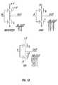
- FIG. 12is an embodiment of an Inverter, AND, and OR logic functions using one type of MEMS switch.
- the embodimentsmay be implemented in or associated with a variety of electronic devices such as, but not limited to, mobile telephones, wireless devices, personal data assistants (PDAs), hand-held or portable computers, GPS receivers/navigators, cameras, MP3 players, camcorders, game consoles, wrist watches, clocks, calculators, television monitors, flat panel displays, computer monitors, auto displays (e.g., odometer display, etc.), cockpit controls and/or displays, display of camera views (e.g., display of a rear view camera in a vehicle), electronic photographs, electronic billboards or signs, projectors, architectural structures, packaging, and aesthetic structures (e.g., display of images on a piece of jewelry).
- MEMS devices of similar structure to those described hereincan also be used in non-display applications such as in electronic switching devices.
- FIG. 1One interferometric modulator display embodiment comprising an interferometric MEMS display element is illustrated in FIG. 1 .
- the pixelsare in either a bright or dark state.
- the display elementIn the bright (“on” or “open”) state, the display element reflects a large portion of incident visible light to a user.
- the dark (“off” or “closed”) stateWhen in the dark (“off” or “closed”) state, the display element reflects little incident visible light to the user.
- the light reflectance properties of the “on” and “off” statesmay be reversed.
- MEMS pixelscan be configured to reflect predominantly at selected colors, allowing for a color display in addition to black and white.
- FIG. 1is an isometric view depicting two adjacent pixels in a series of pixels of a visual display, wherein each pixel comprises a MEMS interferometric modulator.
- an interferometric modulator displaycomprises a row/column array of these interferometric modulators.
- Each interferometric modulatorincludes a pair of reflective layers positioned at a variable and controllable distance from each other to form a resonant optical cavity with at least one variable dimension.
- one of the reflective layersmay be moved between two positions. In the first position, referred to herein as the relaxed, the movable layer is positioned at a relatively large distance from a fixed partially reflective layer.
- the movable layerIn the second position, the movable layer is positioned more closely adjacent to the partially reflective layer. Incident light that reflects from the two layers interferes constructively or destructively depending on the position of the movable reflective layer, producing either an overall reflective or non-reflective state for each pixel.
- the depicted portion of the pixel array in FIG. 1includes two adjacent interferometric modulators 12 a and 12 b .
- a movable and highly reflective layer 14 ais illustrated in a relaxed position at a predetermined distance from a fixed partially reflective layer 16 a .
- the movable highly reflective layer 14 bis illustrated in an actuated position adjacent to the fixed partially reflective layer 16 b.
- the fixed layers 16 a , 16 bare electrically conductive, partially transparent and partially reflective, and may be fabricated, for example, by depositing one or more layers each of chromium and indium-tin-oxide onto a transparent substrate 20 .
- the layersare patterned into parallel strips, and may form row electrodes in a display device as described further below.
- the movable layers 14 a , 14 bmay be formed as a series of parallel strips of a deposited metal layer or layers (orthogonal to the row electrodes 16 a , 16 b ) deposited on top of posts 18 and an intervening sacrificial material deposited between the posts 18 .
- the deformable metal layers 14 a , 14 bare separated from the fixed metal layers by a defined gap 19 .
- a highly conductive and reflective materialsuch as aluminum may be used for the deformable layers, and these strips may form column electrodes in a display device.
- the cavity 19remains between the layers 14 a , 16 a and the deformable layer is in a mechanically relaxed state as illustrated by the pixel 12 a in FIG. 1 .
- the capacitor formed at the intersection of the row and column electrodes at the corresponding pixelbecomes charged, and electrostatic forces pull the electrodes together.
- the movable layeris deformed and is forced against the fixed layer (a dielectric material which is not illustrated in this Figure may be deposited on the fixed layer to prevent shorting and control the separation distance) as illustrated by the pixel 12 b on the right in FIG. 1 .
- the behavioris the same regardless of the polarity of the applied potential difference. In this way, row/column actuation that can control the reflective vs. non-reflective pixel states is analogous in many ways to that used in conventional LCD and other display technologies.
- FIGS. 2 through 5illustrate one exemplary process and system for using an array of interferometric modulators in a display application.
- FIG. 2is a system block diagram illustrating one embodiment of an electronic device that may incorporate aspects of the invention.
- the electronic deviceincludes a processor 21 which may be any general purpose single- or multi-chip microprocessor such as an ARM, Pentium®, Pentium II®, Pentium III®, Pentium IV®, Pentium® Pro, an 8051, a MIPS®, a Power PC®, an ALPHA®, or any special purpose microprocessor such as a digital signal processor, microcontroller, or a programmable gate array.
- the processor 21may be configured to execute one or more software modules.
- the processormay be configured to execute one or more software applications, including a web browser, a telephone application, an email program, or any other software application.
- the processor 21is also configured to communicate with an array controller 22 .
- the array controller 22includes a row driver circuit 24 and a column driver circuit 26 that provide signals to a display array or panel 30 .
- the cross section of the array illustrated in FIG. 1is shown by the lines 1 - 1 in FIG. 2 .
- the row/column actuation protocolmay take advantage of a hysteresis property of these devices illustrated in FIG. 3 . It may require, for example, a 10 volt potential difference to cause a movable layer to deform from the relaxed state to the actuated state. However, when the voltage is reduced from that value, the movable layer maintains its state as the voltage drops back below 10 volts.
- the movable layerdoes not relax completely until the voltage drops below 2 volts.
- There is thus a range of voltage, about 3 to 7 V in the example illustrated in FIG. 3where there exists a window of applied voltage within which the device is stable in either the relaxed or actuated state. This is referred to herein as the “hysteresis window” or “stability window.”
- hysteresis windowor “stability window.”
- the row/column actuation protocolcan be designed such that during row strobing, pixels in the strobed row that are to be actuated are exposed to a voltage difference of about 10 volts, and pixels that are to be relaxed are exposed to a voltage difference of close to zero volts. After the strobe, the pixels are exposed to a steady state voltage difference of about 5 volts such that they remain in whatever state the row strobe put them in. After being written, each pixel sees a potential difference within the “stability window” of 3-7 volts in this example. This feature makes the pixel design illustrated in FIG. 1 stable under the same applied voltage conditions in either an actuated or relaxed pre-existing state.
- each pixel of the interferometric modulatoris essentially a capacitor formed by the fixed and moving reflective layers, this stable state can be held at a voltage within the hysteresis window with almost no power dissipation. Essentially no current flows into the pixel if the applied potential is fixed.
- a display framemay be created by asserting the set of column electrodes in accordance with the desired set of actuated pixels in the first row.
- a row pulseis then applied to the row 1 electrode, actuating the pixels corresponding to the asserted column lines.
- the asserted set of column electrodesis then changed to correspond to the desired set of actuated pixels in the second row.
- a pulseis then applied to the row 2 electrode, actuating the appropriate pixels in row 2 in accordance with the asserted column electrodes.
- the row 1 pixelsare unaffected by the row 2 pulse, and remain in the state they were set to during the row 1 pulse. This may be repeated for the entire series of rows in a sequential fashion to produce the frame.
- the framesare refreshed and/or updated with new display data by continually repeating this process at some desired number of frames per second.
- protocols for driving row and column electrodes of pixel arrays to produce display framesare also well known and may be used in conjunction with the present invention.
- FIGS. 4 and 5illustrate one possible actuation protocol for creating a display frame on the 3 ⁇ 3 array of FIG. 2 .
- FIG. 4illustrates a possible set of column and row voltage levels that may be used for pixels exhibiting the hysteresis curves of FIG. 3 .
- actuating a pixelinvolves setting the appropriate column to ⁇ V bias , and the appropriate row to + ⁇ V, which may correspond to ⁇ 5 volts and +5 volts respectively Relaxing the pixel is accomplished by setting the appropriate column to +V bias , and the appropriate row to the same + ⁇ V, producing a zero volt potential difference across the pixel.
- the pixelsare stable in whatever state they were originally in, regardless of whether the column is at +V bias , or ⁇ V bias .
- voltages of opposite polarity than those described abovecan be used, e.g., actuating a pixel can involve setting the appropriate column to +V bias , and the appropriate row to ⁇ V.
- releasing the pixelis accomplished by setting the appropriate column to ⁇ V bias , and the appropriate row to the same ⁇ V, producing a zero volt potential difference across the pixel.
- FIG. 5Bis a timing diagram showing a series of row and column signals applied to the 3 ⁇ 3 array of FIG. 2 which will result in the display arrangement illustrated in FIG. 5A , where actuated pixels are non-reflective.
- the pixelsPrior to writing the frame illustrated in FIG. 5A , the pixels can be in any state, and in this example, all the rows are at 0 volts, and all the columns are at +5 volts. With these applied voltages, all pixels are stable in their existing actuated or relaxed states.
- pixels ( 1 , 1 ), ( 1 , 2 ), ( 2 , 2 ), ( 3 , 2 ) and ( 3 , 3 )are actuated.
- columns 1 and 2are set to ⁇ 5 volts
- column 3is set to +5 volts. This does not change the state of any pixels, because all the pixels remain in the 3-7 volt stability window.
- Row 1is then strobed with a pulse that goes from 0, up to 5 volts, and back to zero. This actuates the ( 1 , 1 ) and ( 1 , 2 ) pixels and relaxes the ( 1 , 3 ) pixel. No other pixels in the array are affected.
- row 2is set to ⁇ 5 volts, and columns 1 and 3 are set to +5 volts.
- the same strobe applied to row 2will then actuate pixel ( 2 , 2 ) and relax pixels ( 2 , 1 ) and ( 2 , 3 ). Again, no other pixels of the array are affected.
- Row 3is similarly set by setting columns 2 and 3 to ⁇ 5 volts, and column 1 to +5 volts.
- the row 3strobe sets the row 3 pixels as shown in FIG. 5A . After writing the frame, the row potentials are zero, and the column potentials can remain at either +5 or ⁇ 5 volts, and the display is then stable in the arrangement of FIG. 5A .
- FIGS. 6A and 6Bare system block diagrams illustrating an embodiment of a display device 40 .
- the display device 40can be, for example, a cellular or mobile telephone.
- the same components of display device 40 or slight variations thereofare also illustrative of various types of display devices such as televisions and portable media players.
- the display device 40includes a housing 41 , a display 30 , an antenna 43 , a speaker 44 , an input device 48 , and a microphone 46 .
- the housing 41is generally formed from any of a variety of manufacturing processes as are well known to those of skill in the art, including injection molding, and vacuum forming.
- the housing 41may be made from any of a variety of materials, including but not limited to plastic, metal, glass, rubber, and ceramic, or a combination thereof.
- the housing 41includes removable portions (not shown) that may be interchanged with other removable portions of different color, or containing different logos, pictures, or symbols.
- the display 30 of exemplary display device 40may be any of a variety of displays, including a bi-stable display, as described herein.
- the display 30includes a flat-panel display, such as plasma, EL, OLED, STN LCD, or TFT LCD as described above, or a non-flat-panel display, such as a CRT or other tube device, as is well known to those of skill in the art.
- the display 30includes an interferometric modulator display, as described herein.
- the components of one embodiment of exemplary display device 40are schematically illustrated in FIG. 6B .
- the illustrated exemplary display device 40includes a housing 41 and can include additional components at least partially enclosed therein.
- the exemplary display device 40includes a network interface 27 that includes an antenna 43 which is coupled to a transceiver 47 .
- the transceiver 47is connected to a processor 21 , which is connected to conditioning hardware 52 .
- the conditioning hardware 52may be configured to condition a signal (e.g. filter a signal).
- the conditioning hardware 52is connected to a speaker 44 and a microphone 46 .
- the processor 21is also connected to an input device 48 and a driver controller 29 .
- the driver controller 29is coupled to a frame buffer 28 , and to an array driver 22 , which in turn is coupled to a display array 30 .
- a power supply 50provides power to all components as required by the particular exemplary display device 40 design.
- the network interface 27includes the antenna 43 and the transceiver 47 so that the exemplary display device 40 can communicate with one ore more devices over a network. In one embodiment the network interface 27 may also have some processing capabilities to relieve requirements of the processor 21 .
- the antenna 43is any antenna known to those of skill in the art for transmitting and receiving signals. In one embodiment, the antenna transmits and receives RF signals according to the IEEE 802.11 standard, including IEEE 802.11(a), (b), or (g). In another embodiment, the antenna transmits and receives RF signals according to the BLUETOOTH standard. In the case of a cellular telephone, the antenna is designed to receive CDMA, GSM, AMPS or other known signals that are used to communicate within a wireless cell phone network.
- the transceiver 47pre-processes the signals received from the antenna 43 so that they may be received by and further manipulated by the processor 21 .
- the transceiver 47also processes signals received from the processor 21 so that they may be transmitted from the exemplary display device 40 via the antenna 43 .
- the transceiver 47can be replaced by a receiver.
- network interface 27can be replaced by an image source, which can store or generate image data to be sent to the processor 21 .
- the image sourcecan be a digital video disc (DVD) or a hard-disc drive that contains image data, or a software module that generates image data.
- Processor 21generally controls the overall operation of the exemplary display device 40 .
- the processor 21receives data, such as compressed image data from the network interface 27 or an image source, and processes the data into raw image data or into a format that is readily processed into raw image data.
- the processor 21then sends the processed data to the driver controller 29 or to frame buffer 28 for storage.
- Raw datatypically refers to the information that identifies the image characteristics at each location within an image. For example, such image characteristics can include color, saturation, and gray-scale level.
- the processor 21includes a microcontroller, CPU, or logic unit to control operation of the exemplary display device 40 .
- Conditioning hardware 55generally includes amplifiers and filters for transmitting signals to the speaker 44 , and for receiving signals from the microphone 46 .
- Conditioning hardware 55may be discrete components within the exemplary display device 40 , or may be incorporated within the processor 21 or other components.
- the driver controller 29takes the raw image data generated by the processor 21 either directly from the processor 21 or from the frame buffer 28 and reformats the raw image data appropriately for high speed transmission to the array driver 22 . Specifically, the driver controller 29 reformats the raw image data into a data flow having a raster-like format, such that it has a time order suitable for scanning across the display array 30 . Then the driver controller 29 sends the formatted information to the array driver 22 .
- a driver controller 29such as a LCD controller, is often associated with the system processor 21 as a stand-alone Integrated Circuit (IC), such controllers may be implemented in many ways. They may be embedded in the processor 21 as hardware, embedded in the processor 21 as software, or fully integrated in hardware with the array driver 22 .
- the array driver 22receives the formatted information from the driver controller 29 and reformats the video data into a parallel set of waveforms that are applied many times per second to the hundreds and sometimes thousands of leads coming from the display's x-y matrix of pixels.
- driver controller 29is a conventional display controller or a bi-stable display controller (e.g., an interferometric modulator controller).
- array driver 22is a conventional driver or a bi-stable display driver (e.g., an interferometric modulator display).
- a driver controller 29is integrated with the array driver 22 .
- display array 30is a typical display array or a bi-stable display array (e.g., a display including an array of interferometric modulators).
- the input device 48allows a user to control the operation of the exemplary display device 40 .
- input device 48includes a keypad, such as a QWERTY keyboard or a telephone keypad, a button, a switch, a touch-sensitive screen, a pressure- or heat-sensitive membrane.
- the microphone 46is an input device for the exemplary display device 40 . When the microphone 46 is used to input data to the device, voice commands may be provided by a user for controlling operations of the exemplary display device 40 .
- Power supply 50can include a variety of energy storage devices as are well known in the art.
- power supply 50is a rechargeable battery, such as a nickel-cadmium battery or a lithium ion battery.
- power supply 50is a renewable energy source, a capacitor, or a solar cell, including a plastic solar cell, and solar-cell paint.
- power supply 50is configured to receive power from a wall outlet.
- control programmabilityresides, as described above, in a driver controller which can be located in several places in the electronic display system. In some cases control programmability resides in the array driver 22 . Those of skill in the art will recognize that the above-described optimization may be implemented in any number of hardware and/or software components and in various configurations.
- FIGS. 7A-7Cillustrate three different embodiments of the moving mirror structure.
- FIG. 7Ais a cross section of the embodiment of FIG. 1 , where a strip of metal material 14 is deposited on orthogonally extending supports 18 .
- FIG. 7Bthe moveable reflective material 14 is attached to supports at the corners only, on tethers 32 .
- FIG. 7Cthe moveable reflective material 14 is suspended from a deformable layer 34 .
- This embodimenthas benefits because the structural design and materials used for the reflective material 14 can be optimized with respect to the optical properties, and the structural design and materials used for the deformable layer 34 can be optimized with respect to desired mechanical properties.
- FIG. 8Ais a cross-sectional side view of a MEMS switch 700 .
- the MEMS switch 700 of FIG. 8Ahas similar collapsible cavity features as the interferometric modulator of FIG. 7A .
- the MEMS switch 700additionally includes two terminals 706 , an insulating layer 710 , and a conductive strip 708 .
- the MEMS switch 700is a structure that provides selective electrical contact between the two terminals 706 . More particularly, the MEMS switch 700 is considered closed when the terminals 706 are in electrical contact and the MEMS switch is considered open when the terminals 706 are not in electrical contact.
- the MEMS switch 700comprises a moveable material 714 , a conductive strip 708 , and an insulating layer 710 between the moveable material 714 and the conductive strip 708 .
- a substrate 720supports an electrode 702 , and an insulating layer 704 on the electrode 702 .
- Two terminals 706are deposited on and/or through the insulating layer 704 .
- the terminals 706may connect to other circuitry using vias through insulating layer 704 and/or electrode 702 .
- Insulating layer 704 and moveable material 714are mechanically separated by supports 718 in order to define a cavity 707 .
- the moveable material 714is deformable, such that the moveable material 714 may be deformed towards the substrate 720 when a voltage difference is applied across the moveable material 714 and the electrode 702 .
- Thisis analogous to the reflective material 14 , substrate 20 , and electrode 16 of FIG. 7A , and to the reflective layers 14 a and 14 b , the transparent substrate 20 , and the reflective layers 16 a and 16 b of FIG. 1 .
- the moveable material 714may have on it an insulator 710 , which has upon it the conductive strip 708 .
- the conductive strip 708is aligned so that when the moveable material 714 is deflected towards the substrate 720 by an applied potential as described above, the conductive strip 708 contacts both of the terminals 706 , causing the terminals 706 to be in electrical contact and the MEMS switch 700 to be closed.
- the conductive strip 708is electrically isolated from the moveable material 714 by insulator 710 so that contact between the terminals 706 and the movable material 714 does not disturb the voltage difference applied across the moveable material 714 and the electrode 702 .
- the conductive strip 708 and the insulator 710will not be needed, and the moveable material itself 714 can function as the conductor that bridges the two terminals 706 .
- the moveable material 714returns to its mechanically relaxed state and the MEMS switch 700 is opened.
- FIG. 8Bis a top view of MEMS switch 700 .
- the supports 718 , the conductive strip 708 , and the terminals 706are shown as seen looking through the moveable material 714 .
- Conductive strip 708may be significantly smaller than the moveable material 714 . This is to ensure that the electromotive force between the moveable material 714 and the electrode 702 is larger than the electromotive force between the conductive strip 708 and the electrode 702 because once the strip contacts the electrodes, the potential on the strip may differ from the potential on the moveable material.
- FIG. 9is a cross-sectional side view of a MEMS switch 800 of another embodiment.
- MEMS switch 800has similar constructional features as the interferometric modulator of FIG. 7C . It also has MEMS switch functionality and features similar to those of MEMS switch 700 in FIG. 8A .
- MEMS switches built from the same basic structure as interferometric modulatorsease the integration of logic and switching functions with interferometric modulator arrays. It is possible that the other types of switches may be integrated, such as switches fabricated in a manner not similar to the fabrication of the interferometric elements, and more conventional electronic switches fabricated using thin silicon films deposited on the glass substrate. However, because fabrication of interferometric modulator based MEMS switches may be performed using many of the same processing steps that are used in fabricating interferometric modulators, these MEMS switches may be inexpensively integrated onto the same substrate as an array of interferometric modulators used, for example, for a display.
- the MEMS switches and interferometric modulatorsmay be fabricated using the same process, although extra steps may be performed on the interferometric modulators and/or the MEMS switches during the manufacturing process. For example, deposition and etching steps to add terminals to the MEMS switches are unnecessary for the fabrication of interferometric modulators. In such an embodiment some common steps would be performed, such as those for forming the electrodes, etc. The MEMS switch terminals would then be formed. After these steps would follow more steps necessary for both the interferometric modulators and the MEMS switches, thus providing a combined interferometric modulator and MEMS switch array. In yet another embodiment, the same process that is used for manufacturing interferometric modulators is used in manufacturing MEMS switches.
- the interferometric modulatorsmay first be fabricated on a substrate, followed by fabrication of MEMS switches on the substrate.
- MEMS switchesmay first be fabricated on a substrate, followed by fabrication of interferometric modulators on the substrate. In either case, the manufacturing process does not require significant modification as the MEMS switches comprise many of the same structures as the interferometric modulators.
- FIG. 10Ais a schematic circuit diagram illustrating an embodiment of an interferometric modulator array having integrated MEMS switches performing a row select function.
- This row select functionis useful in some display embodiments when it is desired to drive a display having a high row count with a display driver that has fewer row output lines.
- a display with color pixelsmay have 3 times as many columns and 4 times as many rows as a black and white display with the same number of pixels.
- each pixelmay comprise four red, four blue, and four green modulators.
- the reflective states of the set of 12 “sub-pixels”determine the perceived color of the pixel as a whole. For this embodiment, four times as many row driver outputs would normally be necessary.
- the row select functionis used in writing data to the interferometric modulator array.
- data corresponding to states desired for a specific sub-row in the interferometric modulator arrayare driven onto the column lines shared by multiple rows and sub-rows. Subsequently, the specific sub-row for which the data is intended is driven active, thereby causing the interferometric modulators in that sub-row to assume the desired states.
- the principles discussed herecould easily be adapted to perform a column select function for this or another embodiment.
- FIG. 10AA portion of a modulator array is shown in FIG. 10A as display region 45 .
- the term display regionhas been introduced here to specify a certain area of the entire display.
- the display regionis a collection of display elements that typically resolve into a portion of the display presenting a coherent set of image information.
- a typical display regionwould correspond to a single pixel in the resulting image.
- the display region 45 in FIG. 10Acomprises three columns, 62 , 64 , and 66 , typically one for each color such as red, green and blue, in the case where display region 45 represents a pixel; and one row, comprising 4 sub-rows 52 a - d .
- Each sub-row 52 a - dcomprises an interferometric modulator from each of the three columns, and a pair of MEMS switches.
- Driver device 51has one output pin per modulator array row, and a row connection is provided between each driver device 51 output pin and a corresponding row in the modulator array. Row 5 is illustrated in FIGS. 10A and 9B .
- Timing circuit 53sequentially drives each of the timing lines active for a portion of the time that the driver device 50 drives a row active, thereby selecting an active sub-row one at a time. While a timing signal is active the MEMS switch connected to that timing signal and also connected to the bias line B 1 will be open, and the MEMS switch connected to that timing signal and also connected to the row connection will be closed. The signal on the row connection will pass to interferometric modulators of the sub-row 52 a - d .
- Interferometric modulators of an individual sub-row 52 a - dwill be active when: 1) the driver device 51 drives active the row associated with the sub-rows 52 a - d , and 2) the timing circuit 53 drives active the timing signal t 1 -t 4 associated with that particular sub-row 52 a - d.
- the timing circuit 53will sequentially drive each of the timing signals t 1 -t 4 active, each for 1 ⁇ 4 of the time that the row 5 signal is active. While the timing circuit 53 is driving timing signal t 1 active the MEMS switch s 1 will be open and the MEMS switch s 2 will be closed. The interferometric modulators of sub-row 52 a will be connected to the row connection driven by driver device 50 output row 5 . Because output row 5 is active, the interferometric modulators of sub-row 52 a will be driven active. The remaining sub-rows will remain connected to the bias line B 1 .
- Timing circuit 53will then drive timing signal t 2 active, the interferometric modulators of sub-row 52 b will be connected to the row connection driven by output row 5 , and will be driven active. This sequence continues until the sub-rows 52 a - d have each been driven active. Then this sequence repeats for rows 6 , 7 , and so on.
- the timing signalsare shared with all other rows in a column, so that switches for the first sub-row of every row toggle when the first sub-row of any row is active, and so on for the second, third, and fourth sub-rows.
- the driver output pin for the active rowis driven active.
- All non-active rowsare held to a bias voltage while the active row is driven active. In this manner, elements in all sub-rows of the entire array except the active sub-row see the same bias voltage independent of the status of the timing signals and consequently independent of the positions of the switches within the sub-row. It should be observed that switching of the non-active row-select switches could be avoided with masking circuits in cases where further reductions in low power consumption are desired.
- FIG. 10Bshows the circuit of FIG. 10A with the interferometric modulators of display region 45 and the MEMS switches in physical layout view.
- the columns 62 , 64 , 66 , and the sub-rows 52 a - dare indicated.
- the conductive strip 1008 , and the terminals 1006 for each of the MEMS switchesare shown as seen looking through the moveable material 1014 .
- interconnect traces 47to connect the MEMS switches according to the schematic shown in FIG. 10A . Portions of the interconnect routing can be performed underneath the fixed electrodes.
- the traces for the timing lines 49can be routed beneath those, or even on the bottom of the substrate. Connections can be made with vertical vias.
- the MEMS switchescan be fabricated to be the same size as the interferometric modulators. As such, the pitch of the MEMS switches is matched to the pitch of the interferometric modulators. This pitch matching is particularly useful for this embodiment, as well as others which provide signals to each row or to each column. The necessary routing is also conveniently integrated with the interferometric modulators as it can be manufactured using standard metallization interconnect fabrication techniques.
- FIG. 11Ais a schematic circuit diagram illustrating another embodiment of an interferometric modulator array having integrated MEMS switches.
- the MEMS switchesperform a tri-state function.
- This embodimentshows MEMS switches of the same embodiment as that shown in FIGS. 8A , and 8 B, however other MEMS switch embodiments are possible.
- the tri-state functionis useful in the interferometric modulator array system for power savings. While the row and column lines are tri-stated the circuitry used to drive those lines can be powered down. With row and column lines tri-stated, the interferometric modulators in the array will hold the values written to them until the charge slowly dissipates, either across the interferometric modulators or through a non-infinite tri-state open resistance. Because the interferometric modulators can be charged in a small fraction of the time it takes for the charge to dissipate, the driving circuitry can be powered down during a significant fraction of the total display operation time.
- FIG. 11AA portion of a modulator array is shown in FIG. 11A as display region 40 , comprising three columns, 42 , 44 , and 46 , typically one for each color such as red, green and blue, in the case where display region 40 represents a pixel; and one row, comprising 4 sub-rows 52 a - d .
- Each columncomprises a column tri-state MEMS switch, and one interferometric modulator from each sub-row.
- Each sub-row 52 a - dcomprises an interferometric modulator from each of the three columns, and a sub-row tri-state MEMS switch.
- Each of the column and sub-row tri-state MEMS switchesis connected to a signal, HOLD.
- the state of the HOLD signalwill determine whether or not the column and sub-row lines are tri-stated or whether the columns and sub-rows are driven.
- FIG. 11Bshows the circuit of FIG. 11A with the interferometric modulators of display region 40 and the MEMS switches in physical layout view.
- FIG. 11Bis similar to FIG. 9B , and the significant features discussed with regard to FIG. 9B are apparent in FIG. 10B as well. As is the case with FIG. 9B , the ease of integration is also seen by FIG. 10B .
- MEMS switchesmay be used in any application that utilizes switches, whether or not the application also utilizes interferometric modulators.
- an entire substrate, such as glassmay be fabricated with MEMS switches for used in various applications.
- these MEMS switchesmay be used in a manner analogous to transistors. Accordingly, MEMS switches may replace transistors in any application, logic circuits, or controller and driver devices, for example.
- FIG. 12shows embodiments of logic functions using a MEMS switch. Because the MEMS switch is a 4 terminal device with no intrinsic polarity these logic functions may be implemented with only two switches.
- the inverter, AND, and OR gates of FIG. 12each use two MEMS switches with their movable layer connected to the movable layer of the other MEMS switch, forming a first input, and one terminal connected to one terminal of the other MEMS switch, forming an output.
- a first switchhas both its electrode and other terminal connected to supply
- a second switchhas both its electrode and other terminal connected to ground.
- a first switchhas its electrode connected to ground and other terminal connected to a second input, and a second switch has its electrode connected to power and its other terminal connected to ground.
- a first switchhas its electrode connected to ground and other terminal connected to power, and a second switch has its electrode connected to power and its other terminal connected to a second input.
- single type MEMS switchescan be used to create digital logic functions, such as AND, NAND, NOR, OR, XOR, XNOR, and AOI. Other digital logic functions and combinations are also possible.
- MEMS switchesmay be arranged together to provide logical functions typically found in external components, thereby saving system cost.
- MEMS switchesmay be arranged for use in the capacity of low leakage transistors, shift registers, or decoders.
- MEMS switchesmay be used in conjunction with row drivers or column drivers, for example.
- MEMS switchesmay be manufactured on various substrates, such as glass substrates or plastic substrates, for example. The ability to place switches on large area glass substrates is generally less expensive than silicon substrates, providing an advantage over many forms of conventional transistor based logic.
Landscapes
- Engineering & Computer Science (AREA)
- Physics & Mathematics (AREA)
- Computer Hardware Design (AREA)
- General Physics & Mathematics (AREA)
- Theoretical Computer Science (AREA)
- Nonlinear Science (AREA)
- Microelectronics & Electronic Packaging (AREA)
- Optics & Photonics (AREA)
- Mechanical Light Control Or Optical Switches (AREA)
- Devices For Indicating Variable Information By Combining Individual Elements (AREA)
- Micromachines (AREA)
- Control Of Indicators Other Than Cathode Ray Tubes (AREA)
Abstract
Description
Claims (14)
Priority Applications (29)
| Application Number | Priority Date | Filing Date | Title |
|---|---|---|---|
| US11/150,407US7345805B2 (en) | 2004-09-27 | 2005-06-10 | Interferometric modulator array with integrated MEMS electrical switches |
| MYPI20053521AMY142573A (en) | 2004-09-27 | 2005-07-29 | Interferometric modulator array with integrated mems electrical switches |
| AU2005203378AAU2005203378A1 (en) | 2004-09-27 | 2005-08-01 | Interferometric modulator array with integrated MEMS electrical switches |
| TW094127355ATW200634704A (en) | 2004-09-27 | 2005-08-11 | Interferometric modulator array with integrated mems electrical switches |
| JP2005232880AJP4652927B2 (en) | 2004-09-27 | 2005-08-11 | Display device using MEMS switch |
| SG200505164ASG121059A1 (en) | 2004-09-27 | 2005-08-15 | Interferometric modulator array with integrated mems electrical switches |
| SG200906349-6ASG155963A1 (en) | 2004-09-27 | 2005-08-15 | Interferometric modulator array with integrated mems electrical switches |
| CA002517038ACA2517038A1 (en) | 2004-09-27 | 2005-08-25 | Interferometric modulator array with integrated mems electrical switches |
| MXPA05009403AMXPA05009403A (en) | 2004-09-27 | 2005-09-02 | Interferometric modulator array with integrated mems electrical switches. |
| EP05255699AEP1640960B1 (en) | 2004-09-27 | 2005-09-14 | Matrix display with interferometric modulators and integrated MEMS switches |
| DE602005017724TDE602005017724D1 (en) | 2004-09-27 | 2005-09-14 | Matrix display with interferometric modulators and integrated MEMS switches |
| RU2007115895/28ARU2007115895A (en) | 2004-09-27 | 2005-09-14 | MEMS SWITCHES WITH DEFORMABLE MEMBRANES |
| AT05255699TATE449398T1 (en) | 2004-09-27 | 2005-09-14 | MATRIX DISPLAY WITH INTERFEROMETRIC MODULATORS AND INTEGRATED MEMS SWITCHES |
| MX2007003577AMX2007003577A (en) | 2004-09-27 | 2005-09-14 | Mems switches with deforming membranes. |
| PCT/US2005/032782WO2006036560A2 (en) | 2004-09-27 | 2005-09-14 | Mems switches with deforming membranes |
| EP05798437AEP1809568A2 (en) | 2004-09-27 | 2005-09-14 | Mems switches with deforming membranes |
| JP2007533542AJP2008515150A (en) | 2004-09-27 | 2005-09-14 | MEMS switch with deformable thin film |
| CN 200510103444CN1755477B (en) | 2004-09-27 | 2005-09-15 | Interferometric modulator array display device with integrated MEMS electrical switches, and method therefor |
| KR1020050087709AKR101198081B1 (en) | 2004-09-27 | 2005-09-21 | Interferometric modulator array with integrated mems electrical switches |
| BRPI0503935-5ABRPI0503935A (en) | 2004-09-27 | 2005-09-23 | interferometric modulator array with integrated mems electrical switches |
| TW094133425ATW200635845A (en) | 2004-09-27 | 2005-09-26 | MEMS switches with deforming membranes |
| RU2005129913/28ARU2005129913A (en) | 2004-09-27 | 2005-09-26 | MATRIX OF INTERFERENCE MODULATORS WITH INTEGRATED ELECTRIC MEMS-SWITCHES |
| US12/050,094US7859739B2 (en) | 2004-09-27 | 2008-03-17 | Interferometric modulator array with integrated MEMS electrical switches |
| JP2009000342AJP5054040B2 (en) | 2004-09-27 | 2009-01-05 | Interferometric modulator array with integrated MEMS electrical switch |
| US12/961,402US8223424B2 (en) | 2004-09-27 | 2010-12-06 | Interferometric modulator array with integrated MEMS electrical switches |
| US13/528,609US8437071B2 (en) | 2004-09-27 | 2012-06-20 | Interferometric modulator array with integrated MEMS electrical switches |
| KR1020120066149AKR101284822B1 (en) | 2004-09-27 | 2012-06-20 | Interferometric modulator array with integrated mems electrical switches |
| KR1020120107807AKR101290628B1 (en) | 2004-09-27 | 2012-09-27 | Interferometric modulator array with integrated mems electrical switches |
| KR1020130003471AKR20130020816A (en) | 2004-09-27 | 2013-01-11 | Interferometric modulator array with integrated mems electrical switches |
Applications Claiming Priority (2)
| Application Number | Priority Date | Filing Date | Title |
|---|---|---|---|
| US61350104P | 2004-09-27 | 2004-09-27 | |
| US11/150,407US7345805B2 (en) | 2004-09-27 | 2005-06-10 | Interferometric modulator array with integrated MEMS electrical switches |
Related Child Applications (1)
| Application Number | Title | Priority Date | Filing Date |
|---|---|---|---|
| US12/050,094ContinuationUS7859739B2 (en) | 2004-09-27 | 2008-03-17 | Interferometric modulator array with integrated MEMS electrical switches |
Publications (2)
| Publication Number | Publication Date |
|---|---|
| US20060103613A1 US20060103613A1 (en) | 2006-05-18 |
| US7345805B2true US7345805B2 (en) | 2008-03-18 |
Family
ID=35448366
Family Applications (4)
| Application Number | Title | Priority Date | Filing Date |
|---|---|---|---|
| US11/150,407Expired - Fee RelatedUS7345805B2 (en) | 2004-09-27 | 2005-06-10 | Interferometric modulator array with integrated MEMS electrical switches |
| US12/050,094Expired - Fee RelatedUS7859739B2 (en) | 2004-09-27 | 2008-03-17 | Interferometric modulator array with integrated MEMS electrical switches |
| US12/961,402Expired - Fee RelatedUS8223424B2 (en) | 2004-09-27 | 2010-12-06 | Interferometric modulator array with integrated MEMS electrical switches |
| US13/528,609Expired - Fee RelatedUS8437071B2 (en) | 2004-09-27 | 2012-06-20 | Interferometric modulator array with integrated MEMS electrical switches |
Family Applications After (3)
| Application Number | Title | Priority Date | Filing Date |
|---|---|---|---|
| US12/050,094Expired - Fee RelatedUS7859739B2 (en) | 2004-09-27 | 2008-03-17 | Interferometric modulator array with integrated MEMS electrical switches |
| US12/961,402Expired - Fee RelatedUS8223424B2 (en) | 2004-09-27 | 2010-12-06 | Interferometric modulator array with integrated MEMS electrical switches |
| US13/528,609Expired - Fee RelatedUS8437071B2 (en) | 2004-09-27 | 2012-06-20 | Interferometric modulator array with integrated MEMS electrical switches |
Country Status (14)
| Country | Link |
|---|---|
| US (4) | US7345805B2 (en) |
| EP (1) | EP1640960B1 (en) |
| JP (2) | JP4652927B2 (en) |
| KR (4) | KR101198081B1 (en) |
| AT (1) | ATE449398T1 (en) |
| AU (1) | AU2005203378A1 (en) |
| BR (1) | BRPI0503935A (en) |
| CA (1) | CA2517038A1 (en) |
| DE (1) | DE602005017724D1 (en) |
| MX (1) | MXPA05009403A (en) |
| MY (1) | MY142573A (en) |
| RU (1) | RU2005129913A (en) |
| SG (2) | SG121059A1 (en) |
| TW (1) | TW200634704A (en) |
Cited By (22)
| Publication number | Priority date | Publication date | Assignee | Title |
|---|---|---|---|---|
| US20060279495A1 (en)* | 2005-05-05 | 2006-12-14 | Moe Douglas P | Dynamic driver IC and display panel configuration |
| US20080158647A1 (en)* | 2004-09-27 | 2008-07-03 | Idc, Llc | Interferometric modulator array with integrated mems electrical switches |
| US20090237040A1 (en)* | 2008-03-18 | 2009-09-24 | Qualcomm Mems Technologies, Inc. | family of current/power-efficient high voltage linear regulator circuit architectures |
| US20100014146A1 (en)* | 2008-07-17 | 2010-01-21 | Qualcomm Mems Technologies, Inc. | Encapsulation methods for interferometric modulator and mems devices |
| WO2011130715A2 (en) | 2010-04-16 | 2011-10-20 | Flex Lighting Ii, Llc | Illumination device comprising a film-based lightguide |
| WO2011130718A2 (en) | 2010-04-16 | 2011-10-20 | Flex Lighting Ii, Llc | Front illumination device comprising a film-based lightguide |
| US8928967B2 (en) | 1998-04-08 | 2015-01-06 | Qualcomm Mems Technologies, Inc. | Method and device for modulating light |
| US8971675B2 (en) | 2006-01-13 | 2015-03-03 | Qualcomm Mems Technologies, Inc. | Interconnect structure for MEMS device |
| US9110289B2 (en) | 1998-04-08 | 2015-08-18 | Qualcomm Mems Technologies, Inc. | Device for modulating light with multiple electrodes |
| US9116344B2 (en) | 2008-10-27 | 2015-08-25 | Pixtronix, Inc. | MEMS anchors |
| US9128277B2 (en) | 2006-02-23 | 2015-09-08 | Pixtronix, Inc. | Mechanical light modulators with stressed beams |
| US9135868B2 (en) | 2005-02-23 | 2015-09-15 | Pixtronix, Inc. | Direct-view MEMS display devices and methods for generating images thereon |
| US9135867B2 (en) | 2013-04-01 | 2015-09-15 | Pixtronix, Inc. | Display element pixel circuit with voltage equalization |
| US9134552B2 (en) | 2013-03-13 | 2015-09-15 | Pixtronix, Inc. | Display apparatus with narrow gap electrostatic actuators |
| US9158106B2 (en) | 2005-02-23 | 2015-10-13 | Pixtronix, Inc. | Display methods and apparatus |
| US9177523B2 (en) | 2005-02-23 | 2015-11-03 | Pixtronix, Inc. | Circuits for controlling display apparatus |
| US9176318B2 (en) | 2007-05-18 | 2015-11-03 | Pixtronix, Inc. | Methods for manufacturing fluid-filled MEMS displays |
| US9229222B2 (en) | 2005-02-23 | 2016-01-05 | Pixtronix, Inc. | Alignment methods in fluid-filled MEMS displays |
| US9235047B2 (en) | 2011-06-01 | 2016-01-12 | Pixtronix, Inc. | MEMS display pixel control circuits and methods |
| US9261694B2 (en) | 2005-02-23 | 2016-02-16 | Pixtronix, Inc. | Display apparatus and methods for manufacture thereof |
| US9336732B2 (en) | 2005-02-23 | 2016-05-10 | Pixtronix, Inc. | Circuits for controlling display apparatus |
| US9500853B2 (en) | 2005-02-23 | 2016-11-22 | Snaptrack, Inc. | MEMS-based display apparatus |
Families Citing this family (48)
| Publication number | Priority date | Publication date | Assignee | Title |
|---|---|---|---|---|
| US7471444B2 (en) | 1996-12-19 | 2008-12-30 | Idc, Llc | Interferometric modulation of radiation |
| WO2003007049A1 (en)* | 1999-10-05 | 2003-01-23 | Iridigm Display Corporation | Photonic mems and structures |
| US6774426B2 (en)* | 2000-12-19 | 2004-08-10 | Micron Technology, Inc. | Flash cell with trench source-line connection |
| TWI289708B (en) | 2002-12-25 | 2007-11-11 | Qualcomm Mems Technologies Inc | Optical interference type color display |
| US7161728B2 (en)* | 2003-12-09 | 2007-01-09 | Idc, Llc | Area array modulation and lead reduction in interferometric modulators |
| US7342705B2 (en) | 2004-02-03 | 2008-03-11 | Idc, Llc | Spatial light modulator with integrated optical compensation structure |
| US7499208B2 (en)* | 2004-08-27 | 2009-03-03 | Udc, Llc | Current mode display driver circuit realization feature |
| US7515147B2 (en) | 2004-08-27 | 2009-04-07 | Idc, Llc | Staggered column drive circuit systems and methods |
| US7889163B2 (en) | 2004-08-27 | 2011-02-15 | Qualcomm Mems Technologies, Inc. | Drive method for MEMS devices |
| US7551159B2 (en)* | 2004-08-27 | 2009-06-23 | Idc, Llc | System and method of sensing actuation and release voltages of an interferometric modulator |
| US7560299B2 (en) | 2004-08-27 | 2009-07-14 | Idc, Llc | Systems and methods of actuating MEMS display elements |
| US8310441B2 (en) | 2004-09-27 | 2012-11-13 | Qualcomm Mems Technologies, Inc. | Method and system for writing data to MEMS display elements |
| AU2005289445A1 (en) | 2004-09-27 | 2006-04-06 | Idc, Llc | Method and device for multistate interferometric light modulation |
| US7545550B2 (en) | 2004-09-27 | 2009-06-09 | Idc, Llc | Systems and methods of actuating MEMS display elements |
| US7532195B2 (en) | 2004-09-27 | 2009-05-12 | Idc, Llc | Method and system for reducing power consumption in a display |
| US7843410B2 (en) | 2004-09-27 | 2010-11-30 | Qualcomm Mems Technologies, Inc. | Method and device for electrically programmable display |
| US8878825B2 (en) | 2004-09-27 | 2014-11-04 | Qualcomm Mems Technologies, Inc. | System and method for providing a variable refresh rate of an interferometric modulator display |
| US7310179B2 (en)* | 2004-09-27 | 2007-12-18 | Idc, Llc | Method and device for selective adjustment of hysteresis window |
| US7679627B2 (en)* | 2004-09-27 | 2010-03-16 | Qualcomm Mems Technologies, Inc. | Controller and driver features for bi-stable display |
| US7136213B2 (en) | 2004-09-27 | 2006-11-14 | Idc, Llc | Interferometric modulators having charge persistence |
| US7446927B2 (en) | 2004-09-27 | 2008-11-04 | Idc, Llc | MEMS switch with set and latch electrodes |
| US7675669B2 (en)* | 2004-09-27 | 2010-03-09 | Qualcomm Mems Technologies, Inc. | Method and system for driving interferometric modulators |
| US7626581B2 (en) | 2004-09-27 | 2009-12-01 | Idc, Llc | Device and method for display memory using manipulation of mechanical response |
| US7724993B2 (en) | 2004-09-27 | 2010-05-25 | Qualcomm Mems Technologies, Inc. | MEMS switches with deforming membranes |
| US7948457B2 (en) | 2005-05-05 | 2011-05-24 | Qualcomm Mems Technologies, Inc. | Systems and methods of actuating MEMS display elements |
| US7920136B2 (en) | 2005-05-05 | 2011-04-05 | Qualcomm Mems Technologies, Inc. | System and method of driving a MEMS display device |
| US7355779B2 (en) | 2005-09-02 | 2008-04-08 | Idc, Llc | Method and system for driving MEMS display elements |
| US20070126673A1 (en)* | 2005-12-07 | 2007-06-07 | Kostadin Djordjev | Method and system for writing data to MEMS display elements |
| US8391630B2 (en) | 2005-12-22 | 2013-03-05 | Qualcomm Mems Technologies, Inc. | System and method for power reduction when decompressing video streams for interferometric modulator displays |
| US7427201B2 (en) | 2006-01-12 | 2008-09-23 | Green Cloak Llc | Resonant frequency filtered arrays for discrete addressing of a matrix |
| US8194056B2 (en) | 2006-02-09 | 2012-06-05 | Qualcomm Mems Technologies Inc. | Method and system for writing data to MEMS display elements |
| US8049713B2 (en) | 2006-04-24 | 2011-11-01 | Qualcomm Mems Technologies, Inc. | Power consumption optimized display update |
| US7777715B2 (en) | 2006-06-29 | 2010-08-17 | Qualcomm Mems Technologies, Inc. | Passive circuits for de-multiplexing display inputs |
| EP1943555B1 (en) | 2006-10-06 | 2012-05-02 | QUALCOMM MEMS Technologies, Inc. | Optical loss structure integrated in an illumination apparatus of a display |
| EP1943551A2 (en) | 2006-10-06 | 2008-07-16 | Qualcomm Mems Technologies, Inc. | Light guide |
| US7684106B2 (en) | 2006-11-02 | 2010-03-23 | Qualcomm Mems Technologies, Inc. | Compatible MEMS switch architecture |
| US7724417B2 (en)* | 2006-12-19 | 2010-05-25 | Qualcomm Mems Technologies, Inc. | MEMS switches with deforming membranes |
| US7556981B2 (en) | 2006-12-29 | 2009-07-07 | Qualcomm Mems Technologies, Inc. | Switches for shorting during MEMS etch release |
| US9697763B2 (en) | 2007-02-07 | 2017-07-04 | Meisner Consulting Inc. | Displays including addressible trace structures |
| US20080192029A1 (en)* | 2007-02-08 | 2008-08-14 | Michael Hugh Anderson | Passive circuits for de-multiplexing display inputs |
| US8022896B2 (en)* | 2007-08-08 | 2011-09-20 | Qualcomm Mems Technologies, Inc. | ESD protection for MEMS display panels |
| US8068710B2 (en)* | 2007-12-07 | 2011-11-29 | Qualcomm Mems Technologies, Inc. | Decoupled holographic film and diffuser |
| US8736590B2 (en) | 2009-03-27 | 2014-05-27 | Qualcomm Mems Technologies, Inc. | Low voltage driver scheme for interferometric modulators |
| JP5310529B2 (en)* | 2009-12-22 | 2013-10-09 | 株式会社豊田中央研究所 | Oscillator for plate member |
| US20120153970A1 (en)* | 2010-12-21 | 2012-06-21 | Qualcomm Mems Technologies, Inc. | Capacitive touch sensing devices and methods of manufacturing thereof |
| US8836681B2 (en)* | 2011-10-21 | 2014-09-16 | Qualcomm Mems Technologies, Inc. | Method and device for reducing effect of polarity inversion in driving display |
| US9127992B2 (en)* | 2013-03-06 | 2015-09-08 | Ricoh Company, Ltd. | Wide-area pressure sensor with reduced power consumption |
| JPWO2018051946A1 (en)* | 2016-09-16 | 2019-07-04 | 日本電気株式会社 | Integrated circuit |
Citations (280)
| Publication number | Priority date | Publication date | Assignee | Title |
|---|---|---|---|---|
| US3982239A (en) | 1973-02-07 | 1976-09-21 | North Hills Electronics, Inc. | Saturation drive arrangements for optically bistable displays |
| US4403248A (en) | 1980-03-04 | 1983-09-06 | U.S. Philips Corporation | Display device with deformable reflective medium |
| US4441791A (en) | 1980-09-02 | 1984-04-10 | Texas Instruments Incorporated | Deformable mirror light modulator |
| US4482213A (en) | 1982-11-23 | 1984-11-13 | Texas Instruments Incorporated | Perimeter seal reinforcement holes for plastic LCDs |
| US4500171A (en) | 1982-06-02 | 1985-02-19 | Texas Instruments Incorporated | Process for plastic LCD fill hole sealing |
| US4519676A (en) | 1982-02-01 | 1985-05-28 | U.S. Philips Corporation | Passive display device |
| US4566935A (en) | 1984-07-31 | 1986-01-28 | Texas Instruments Incorporated | Spatial light modulator and method |
| US4571603A (en) | 1981-11-03 | 1986-02-18 | Texas Instruments Incorporated | Deformable mirror electrostatic printer |
| US4596992A (en) | 1984-08-31 | 1986-06-24 | Texas Instruments Incorporated | Linear spatial light modulator and printer |
| US4615595A (en) | 1984-10-10 | 1986-10-07 | Texas Instruments Incorporated | Frame addressed spatial light modulator |
| US4662746A (en) | 1985-10-30 | 1987-05-05 | Texas Instruments Incorporated | Spatial light modulator and method |
| US4681403A (en) | 1981-07-16 | 1987-07-21 | U.S. Philips Corporation | Display device with micromechanical leaf spring switches |
| US4710732A (en) | 1984-07-31 | 1987-12-01 | Texas Instruments Incorporated | Spatial light modulator and method |
| US4709995A (en) | 1984-08-18 | 1987-12-01 | Canon Kabushiki Kaisha | Ferroelectric display panel and driving method therefor to achieve gray scale |
| EP0300754A2 (en) | 1987-07-21 | 1989-01-25 | THORN EMI plc | Display device |
| EP0306308A2 (en) | 1987-09-04 | 1989-03-08 | New York Institute Of Technology | Video display apparatus |
| US4856863A (en) | 1988-06-22 | 1989-08-15 | Texas Instruments Incorporated | Optical fiber interconnection network including spatial light modulator |
| US4859060A (en) | 1985-11-26 | 1989-08-22 | 501 Sharp Kabushiki Kaisha | Variable interferometric device and a process for the production of the same |
| US4954789A (en) | 1989-09-28 | 1990-09-04 | Texas Instruments Incorporated | Spatial light modulator |
| US4956619A (en) | 1988-02-19 | 1990-09-11 | Texas Instruments Incorporated | Spatial light modulator |
| US4982184A (en) | 1989-01-03 | 1991-01-01 | General Electric Company | Electrocrystallochromic display and element |
| US5018256A (en) | 1990-06-29 | 1991-05-28 | Texas Instruments Incorporated | Architecture and process for integrating DMD with control circuit substrates |
| US5028939A (en) | 1988-08-23 | 1991-07-02 | Texas Instruments Incorporated | Spatial light modulator system |
| US5037173A (en) | 1989-11-22 | 1991-08-06 | Texas Instruments Incorporated | Optical interconnection network |
| US5055833A (en) | 1986-10-17 | 1991-10-08 | Thomson Grand Public | Method for the control of an electro-optical matrix screen and control circuit |
| US5061049A (en) | 1984-08-31 | 1991-10-29 | Texas Instruments Incorporated | Spatial light modulator and method |
| US5078479A (en) | 1990-04-20 | 1992-01-07 | Centre Suisse D'electronique Et De Microtechnique Sa | Light modulation device with matrix addressing |
| US5079544A (en) | 1989-02-27 | 1992-01-07 | Texas Instruments Incorporated | Standard independent digitized video system |
| US5083857A (en) | 1990-06-29 | 1992-01-28 | Texas Instruments Incorporated | Multi-level deformable mirror device |
| US5096279A (en) | 1984-08-31 | 1992-03-17 | Texas Instruments Incorporated | Spatial light modulator and method |
| US5099353A (en) | 1990-06-29 | 1992-03-24 | Texas Instruments Incorporated | Architecture and process for integrating DMD with control circuit substrates |
| US5124834A (en) | 1989-11-16 | 1992-06-23 | General Electric Company | Transferrable, self-supporting pellicle for elastomer light valve displays and method for making the same |
| US5142414A (en) | 1991-04-22 | 1992-08-25 | Koehler Dale R | Electrically actuatable temporal tristimulus-color device |
| US5142405A (en) | 1990-06-29 | 1992-08-25 | Texas Instruments Incorporated | Bistable dmd addressing circuit and method |
| US5162787A (en) | 1989-02-27 | 1992-11-10 | Texas Instruments Incorporated | Apparatus and method for digitized video system utilizing a moving display surface |
| US5168406A (en) | 1991-07-31 | 1992-12-01 | Texas Instruments Incorporated | Color deformable mirror device and method for manufacture |
| US5170156A (en) | 1989-02-27 | 1992-12-08 | Texas Instruments Incorporated | Multi-frequency two dimensional display system |
| US5172262A (en) | 1985-10-30 | 1992-12-15 | Texas Instruments Incorporated | Spatial light modulator and method |
| US5179274A (en) | 1991-07-12 | 1993-01-12 | Texas Instruments Incorporated | Method for controlling operation of optical systems and devices |
| US5192395A (en) | 1990-10-12 | 1993-03-09 | Texas Instruments Incorporated | Method of making a digital flexure beam accelerometer |
| US5192946A (en) | 1989-02-27 | 1993-03-09 | Texas Instruments Incorporated | Digitized color video display system |
| US5206629A (en) | 1989-02-27 | 1993-04-27 | Texas Instruments Incorporated | Spatial light modulator and memory for digitized video display |
| US5212582A (en) | 1992-03-04 | 1993-05-18 | Texas Instruments Incorporated | Electrostatically controlled beam steering device and method |
| US5214419A (en) | 1989-02-27 | 1993-05-25 | Texas Instruments Incorporated | Planarized true three dimensional display |
| US5214420A (en) | 1989-02-27 | 1993-05-25 | Texas Instruments Incorporated | Spatial light modulator projection system with random polarity light |
| US5216537A (en) | 1990-06-29 | 1993-06-01 | Texas Instruments Incorporated | Architecture and process for integrating DMD with control circuit substrates |
| US5226099A (en) | 1991-04-26 | 1993-07-06 | Texas Instruments Incorporated | Digital micromirror shutter device |
| US5227900A (en) | 1990-03-20 | 1993-07-13 | Canon Kabushiki Kaisha | Method of driving ferroelectric liquid crystal element |
| US5231532A (en) | 1992-02-05 | 1993-07-27 | Texas Instruments Incorporated | Switchable resonant filter for optical radiation |
| US5233456A (en) | 1991-12-20 | 1993-08-03 | Texas Instruments Incorporated | Resonant mirror and method of manufacture |
| US5233459A (en) | 1991-03-06 | 1993-08-03 | Massachusetts Institute Of Technology | Electric display device |
| US5233385A (en) | 1991-12-18 | 1993-08-03 | Texas Instruments Incorporated | White light enhanced color field sequential projection |
| US5254980A (en) | 1991-09-06 | 1993-10-19 | Texas Instruments Incorporated | DMD display system controller |
| US5272473A (en) | 1989-02-27 | 1993-12-21 | Texas Instruments Incorporated | Reduced-speckle display system |
| US5278652A (en) | 1991-04-01 | 1994-01-11 | Texas Instruments Incorporated | DMD architecture and timing for use in a pulse width modulated display system |
| US5280277A (en) | 1990-06-29 | 1994-01-18 | Texas Instruments Incorporated | Field updated deformable mirror device |
| US5287215A (en) | 1991-07-17 | 1994-02-15 | Optron Systems, Inc. | Membrane light modulation systems |
| US5287096A (en) | 1989-02-27 | 1994-02-15 | Texas Instruments Incorporated | Variable luminosity display system |
| US5296950A (en) | 1992-01-31 | 1994-03-22 | Texas Instruments Incorporated | Optical signal free-space conversion board |
| US5312513A (en) | 1992-04-03 | 1994-05-17 | Texas Instruments Incorporated | Methods of forming multiple phase light modulators |
| US5323002A (en) | 1992-03-25 | 1994-06-21 | Texas Instruments Incorporated | Spatial light modulator based optical calibration system |
| US5325116A (en) | 1992-09-18 | 1994-06-28 | Texas Instruments Incorporated | Device for writing to and reading from optical storage media |
| US5327286A (en) | 1992-08-31 | 1994-07-05 | Texas Instruments Incorporated | Real time optical correlation system |
| US5331454A (en) | 1990-11-13 | 1994-07-19 | Texas Instruments Incorporated | Low reset voltage process for DMD |
| EP0608056A1 (en) | 1993-01-11 | 1994-07-27 | Canon Kabushiki Kaisha | Display line dispatcher apparatus |
| US5365283A (en) | 1993-07-19 | 1994-11-15 | Texas Instruments Incorporated | Color phase control for projection display using spatial light modulator |
| EP0655725A1 (en) | 1993-11-30 | 1995-05-31 | Rohm Co., Ltd. | Method and apparatus for reducing power consumption in a matrix display |
| EP0667548A1 (en) | 1994-01-27 | 1995-08-16 | AT&T Corp. | Micromechanical modulator |
| US5444566A (en) | 1994-03-07 | 1995-08-22 | Texas Instruments Incorporated | Optimized electronic operation of digital micromirror devices |
| US5446479A (en) | 1989-02-27 | 1995-08-29 | Texas Instruments Incorporated | Multi-dimensional array video processor system |
| US5448314A (en) | 1994-01-07 | 1995-09-05 | Texas Instruments | Method and apparatus for sequential color imaging |
| US5452024A (en) | 1993-11-01 | 1995-09-19 | Texas Instruments Incorporated | DMD display system |
| US5454906A (en) | 1994-06-21 | 1995-10-03 | Texas Instruments Inc. | Method of providing sacrificial spacer for micro-mechanical devices |
| US5457566A (en) | 1991-11-22 | 1995-10-10 | Texas Instruments Incorporated | DMD scanner |
| US5457493A (en) | 1993-09-15 | 1995-10-10 | Texas Instruments Incorporated | Digital micro-mirror based image simulation system |
| US5459602A (en) | 1993-10-29 | 1995-10-17 | Texas Instruments | Micro-mechanical optical shutter |
| US5461411A (en) | 1993-03-29 | 1995-10-24 | Texas Instruments Incorporated | Process and architecture for digital micromirror printer |
| WO1995030924A1 (en) | 1994-05-05 | 1995-11-16 | Etalon, Inc. | Visible spectrum modulator arrays |
| US5488505A (en) | 1992-10-01 | 1996-01-30 | Engle; Craig D. | Enhanced electrostatic shutter mosaic modulator |
| US5489952A (en) | 1993-07-14 | 1996-02-06 | Texas Instruments Incorporated | Method and device for multi-format television |
| US5497172A (en) | 1994-06-13 | 1996-03-05 | Texas Instruments Incorporated | Pulse width modulation for spatial light modulator with split reset addressing |
| US5497197A (en) | 1993-11-04 | 1996-03-05 | Texas Instruments Incorporated | System and method for packaging data into video processor |
| US5499062A (en) | 1994-06-23 | 1996-03-12 | Texas Instruments Incorporated | Multiplexed memory timing with block reset and secondary memory |
| US5506597A (en) | 1989-02-27 | 1996-04-09 | Texas Instruments Incorporated | Apparatus and method for image projection |
| US5517347A (en) | 1993-12-01 | 1996-05-14 | Texas Instruments Incorporated | Direct view deformable mirror device |
| US5526172A (en) | 1993-07-27 | 1996-06-11 | Texas Instruments Incorporated | Microminiature, monolithic, variable electrical signal processor and apparatus including same |
| US5526051A (en) | 1993-10-27 | 1996-06-11 | Texas Instruments Incorporated | Digital television system |
| US5526688A (en) | 1990-10-12 | 1996-06-18 | Texas Instruments Incorporated | Digital flexure beam accelerometer and method |
| US5535047A (en) | 1995-04-18 | 1996-07-09 | Texas Instruments Incorporated | Active yoke hidden hinge digital micromirror device |
| EP0725380A1 (en) | 1995-01-31 | 1996-08-07 | Canon Kabushiki Kaisha | Display control method for display apparatus having maintainability of display-status function and display control system |
| US5548301A (en) | 1993-01-11 | 1996-08-20 | Texas Instruments Incorporated | Pixel control circuitry for spatial light modulator |
| US5552925A (en) | 1993-09-07 | 1996-09-03 | John M. Baker | Electro-micro-mechanical shutters on transparent substrates |
| US5552924A (en) | 1994-11-14 | 1996-09-03 | Texas Instruments Incorporated | Micromechanical device having an improved beam |
| US5563398A (en) | 1991-10-31 | 1996-10-08 | Texas Instruments Incorporated | Spatial light modulator scanning system |
| US5567334A (en) | 1995-02-27 | 1996-10-22 | Texas Instruments Incorporated | Method for creating a digital micromirror device using an aluminum hard mask |
| US5578976A (en) | 1995-06-22 | 1996-11-26 | Rockwell International Corporation | Micro electromechanical RF switch |
| US5581272A (en) | 1993-08-25 | 1996-12-03 | Texas Instruments Incorporated | Signal generator for controlling a spatial light modulator |
| US5583688A (en) | 1993-12-21 | 1996-12-10 | Texas Instruments Incorporated | Multi-level digital micromirror device |
| US5598565A (en) | 1993-12-29 | 1997-01-28 | Intel Corporation | Method and apparatus for screen power saving |
| US5597736A (en) | 1992-08-11 | 1997-01-28 | Texas Instruments Incorporated | High-yield spatial light modulator with light blocking layer |
| US5602671A (en) | 1990-11-13 | 1997-02-11 | Texas Instruments Incorporated | Low surface energy passivation layer for micromechanical devices |
| US5610624A (en) | 1994-11-30 | 1997-03-11 | Texas Instruments Incorporated | Spatial light modulator with reduced possibility of an on state defect |
| US5610438A (en) | 1995-03-08 | 1997-03-11 | Texas Instruments Incorporated | Micro-mechanical device with non-evaporable getter |
| US5610625A (en) | 1992-05-20 | 1997-03-11 | Texas Instruments Incorporated | Monolithic spatial light modulator and memory package |
| US5612713A (en) | 1995-01-06 | 1997-03-18 | Texas Instruments Incorporated | Digital micro-mirror device with block data loading |
| US5619061A (en) | 1993-07-27 | 1997-04-08 | Texas Instruments Incorporated | Micromechanical microwave switching |
| US5619365A (en) | 1992-06-08 | 1997-04-08 | Texas Instruments Incorporated | Elecronically tunable optical periodic surface filters with an alterable resonant frequency |
| US5629790A (en) | 1993-10-18 | 1997-05-13 | Neukermans; Armand P. | Micromachined torsional scanner |
| WO1997017628A1 (en) | 1995-11-06 | 1997-05-15 | Etalon, Inc. | Interferometric modulation |
| US5633652A (en) | 1984-02-17 | 1997-05-27 | Canon Kabushiki Kaisha | Method for driving optical modulation device |
| US5636052A (en) | 1994-07-29 | 1997-06-03 | Lucent Technologies Inc. | Direct view display based on a micromechanical modulation |
| US5638084A (en) | 1992-05-22 | 1997-06-10 | Dielectric Systems International, Inc. | Lighting-independent color video display |
| US5638946A (en) | 1996-01-11 | 1997-06-17 | Northeastern University | Micromechanical switch with insulated switch contact |
| US5646768A (en) | 1994-07-29 | 1997-07-08 | Texas Instruments Incorporated | Support posts for micro-mechanical devices |
| US5650881A (en) | 1994-11-02 | 1997-07-22 | Texas Instruments Incorporated | Support post architecture for micromechanical devices |
| US5654741A (en) | 1994-05-17 | 1997-08-05 | Texas Instruments Incorporation | Spatial light modulator display pointing device |
| US5659374A (en) | 1992-10-23 | 1997-08-19 | Texas Instruments Incorporated | Method of repairing defective pixels |
| US5665997A (en) | 1994-03-31 | 1997-09-09 | Texas Instruments Incorporated | Grated landing area to eliminate sticking of micro-mechanical devices |
| US5745281A (en) | 1995-12-29 | 1998-04-28 | Hewlett-Packard Company | Electrostatically-driven light modulator and display |
| US5754160A (en) | 1994-04-18 | 1998-05-19 | Casio Computer Co., Ltd. | Liquid crystal display device having a plurality of scanning methods |
| US5771116A (en) | 1996-10-21 | 1998-06-23 | Texas Instruments Incorporated | Multiple bias level reset waveform for enhanced DMD control |
| EP0852371A1 (en) | 1995-09-20 | 1998-07-08 | Hitachi, Ltd. | Image display device |
| US5808780A (en) | 1997-06-09 | 1998-09-15 | Texas Instruments Incorporated | Non-contacting micromechanical optical switch |
| US5842088A (en) | 1994-06-17 | 1998-11-24 | Texas Instruments Incorporated | Method of calibrating a spatial light modulator printing system |
| US5867302A (en) | 1997-08-07 | 1999-02-02 | Sandia Corporation | Bistable microelectromechanical actuator |
| EP0911794A1 (en) | 1997-10-16 | 1999-04-28 | Sharp Kabushiki Kaisha | Display device and method of addressing the same with simultaneous addressing of groups of strobe electrodes and pairs of data electrodes in combination |
| US5912758A (en) | 1996-09-11 | 1999-06-15 | Texas Instruments Incorporated | Bipolar reset for spatial light modulators |
| US5943158A (en) | 1998-05-05 | 1999-08-24 | Lucent Technologies Inc. | Micro-mechanical, anti-reflection, switched optical modulator array and fabrication method |
| US5966235A (en) | 1997-09-30 | 1999-10-12 | Lucent Technologies, Inc. | Micro-mechanical modulator having an improved membrane configuration |
| WO1999052006A3 (en) | 1998-04-08 | 1999-12-29 | Etalon Inc | Interferometric modulation of radiation |
| US6028690A (en) | 1997-11-26 | 2000-02-22 | Texas Instruments Incorporated | Reduced micromirror mirror gaps for improved contrast ratio |
| US6038056A (en) | 1997-05-08 | 2000-03-14 | Texas Instruments Incorporated | Spatial light modulator having improved contrast ratio |
| US6040937A (en) | 1994-05-05 | 2000-03-21 | Etalon, Inc. | Interferometric modulation |
| US6061075A (en) | 1992-01-23 | 2000-05-09 | Texas Instruments Incorporated | Non-systolic time delay and integration printing |
| US6099132A (en) | 1994-09-23 | 2000-08-08 | Texas Instruments Incorporated | Manufacture method for micromechanical devices |
| US6100872A (en) | 1993-05-25 | 2000-08-08 | Canon Kabushiki Kaisha | Display control method and apparatus |
| US6113239A (en) | 1998-09-04 | 2000-09-05 | Sharp Laboratories Of America, Inc. | Projection display system for reflective light valves |
| US6147790A (en) | 1998-06-02 | 2000-11-14 | Texas Instruments Incorporated | Spring-ring micromechanical device |
| US6160833A (en) | 1998-05-06 | 2000-12-12 | Xerox Corporation | Blue vertical cavity surface emitting laser |
| US6180428B1 (en) | 1997-12-12 | 2001-01-30 | Xerox Corporation | Monolithic scanning light emitting devices using micromachining |
| US6201633B1 (en) | 1999-06-07 | 2001-03-13 | Xerox Corporation | Micro-electromechanical based bistable color display sheets |
| US6232936B1 (en) | 1993-12-03 | 2001-05-15 | Texas Instruments Incorporated | DMD Architecture to improve horizontal resolution |
| US20010003487A1 (en) | 1996-11-05 | 2001-06-14 | Mark W. Miles | Visible spectrum modulator arrays |
| US6275326B1 (en) | 1999-09-21 | 2001-08-14 | Lucent Technologies Inc. | Control arrangement for microelectromechanical devices and systems |
| US6282010B1 (en) | 1998-05-14 | 2001-08-28 | Texas Instruments Incorporated | Anti-reflective coatings for spatial light modulators |
| US6295154B1 (en) | 1998-06-05 | 2001-09-25 | Texas Instruments Incorporated | Optical switching apparatus |
| US6304297B1 (en) | 1998-07-21 | 2001-10-16 | Ati Technologies, Inc. | Method and apparatus for manipulating display of update rate |
| US20010034075A1 (en) | 2000-02-08 | 2001-10-25 | Shigeru Onoya | Semiconductor device and method of driving semiconductor device |
| US20010043171A1 (en) | 2000-02-24 | 2001-11-22 | Van Gorkom Gerardus Gegorius Petrus | Display device comprising a light guide |
| US6323982B1 (en) | 1998-05-22 | 2001-11-27 | Texas Instruments Incorporated | Yield superstructure for digital micromirror device |
| US20010046081A1 (en) | 2000-01-31 | 2001-11-29 | Naoyuki Hayashi | Sheet-like display, sphere-like resin body, and micro-capsule |
| US6327071B1 (en) | 1998-10-16 | 2001-12-04 | Fuji Photo Film Co., Ltd. | Drive methods of array-type light modulation element and flat-panel display |
| US20010051014A1 (en) | 2000-03-24 | 2001-12-13 | Behrang Behin | Optical switch employing biased rotatable combdrive devices and methods |
| US20020000959A1 (en) | 1998-10-08 | 2002-01-03 | International Business Machines Corporation | Micromechanical displays and fabrication method |
| US20020005827A1 (en) | 2000-06-13 | 2002-01-17 | Fuji Xerox Co. Ltd. | Photo-addressable type recording display apparatus |
| US20020012159A1 (en) | 1999-12-30 | 2002-01-31 | Tew Claude E. | Analog pulse width modulation cell for digital micromechanical device |
| US20020015215A1 (en) | 1994-05-05 | 2002-02-07 | Iridigm Display Corporation, A Delaware Corporation | Interferometric modulation of radiation |
| US20020024711A1 (en) | 1994-05-05 | 2002-02-28 | Iridigm Display Corporation, A Delaware Corporation | Interferometric modulation of radiation |
| US6356254B1 (en) | 1998-09-25 | 2002-03-12 | Fuji Photo Film Co., Ltd. | Array-type light modulating device and method of operating flat display unit |
| US6356085B1 (en) | 2000-05-09 | 2002-03-12 | Pacesetter, Inc. | Method and apparatus for converting capacitance to voltage |
| US20020036304A1 (en) | 1998-11-25 | 2002-03-28 | Raytheon Company, A Delaware Corporation | Method and apparatus for switching high frequency signals |
| US20020050882A1 (en) | 2000-10-27 | 2002-05-02 | Hyman Daniel J. | Microfabricated double-throw relay with multimorph actuator and electrostatic latch mechanism |
| US20020054424A1 (en)* | 1994-05-05 | 2002-05-09 | Etalon, Inc. | Photonic mems and structures |
| US20020075226A1 (en) | 2000-12-19 | 2002-06-20 | Lippincott Louis A. | Obtaining a high refresh rate display using a low bandwidth digital interface |
| US20020093722A1 (en) | 2000-12-01 | 2002-07-18 | Edward Chan | Driver and method of operating a micro-electromechanical system device |
| US20020097133A1 (en) | 2000-12-27 | 2002-07-25 | Commissariat A L'energie Atomique | Micro-device with thermal actuator |
| US6429601B1 (en) | 1998-02-18 | 2002-08-06 | Cambridge Display Technology Ltd. | Electroluminescent devices |
| US6433917B1 (en) | 2000-11-22 | 2002-08-13 | Ball Semiconductor, Inc. | Light modulation device and system |
| US6465355B1 (en) | 2001-04-27 | 2002-10-15 | Hewlett-Packard Company | Method of fabricating suspended microstructures |
| US6473274B1 (en) | 2000-06-28 | 2002-10-29 | Texas Instruments Incorporated | Symmetrical microactuator structure for use in mass data storage devices, or the like |
| US6480177B2 (en) | 1997-06-04 | 2002-11-12 | Texas Instruments Incorporated | Blocked stepped address voltage for micromechanical devices |
| US20020179421A1 (en) | 2001-04-26 | 2002-12-05 | Williams Byron L. | Mechanically assisted restoring force support for micromachined membranes |
| US20020186108A1 (en) | 2001-04-02 | 2002-12-12 | Paul Hallbjorner | Micro electromechanical switches |
| US6496122B2 (en) | 1998-06-26 | 2002-12-17 | Sharp Laboratories Of America, Inc. | Image display and remote control system capable of displaying two distinct images |
| US6501107B1 (en) | 1998-12-02 | 2002-12-31 | Microsoft Corporation | Addressable fuse array for circuits and mechanical devices |
| US20030004272A1 (en) | 2000-03-01 | 2003-01-02 | Power Mark P J | Data transfer method and apparatus |
| US6507330B1 (en) | 1999-09-01 | 2003-01-14 | Displaytech, Inc. | DC-balanced and non-DC-balanced drive schemes for liquid crystal devices |
| US6507331B1 (en) | 1999-05-27 | 2003-01-14 | Koninklijke Philips Electronics N.V. | Display device |
| WO2003007049A1 (en) | 1999-10-05 | 2003-01-23 | Iridigm Display Corporation | Photonic mems and structures |
| WO2003015071A2 (en) | 2001-08-03 | 2003-02-20 | Sendo International Limited | Image refresh in a display |
| US6545335B1 (en) | 1999-12-27 | 2003-04-08 | Xerox Corporation | Structure and method for electrical isolation of optoelectronic integrated circuits |
| US6548908B2 (en) | 1999-12-27 | 2003-04-15 | Xerox Corporation | Structure and method for planar lateral oxidation in passive devices |
| US6549338B1 (en) | 1999-11-12 | 2003-04-15 | Texas Instruments Incorporated | Bandpass filter to reduce thermal impact of dichroic light shift |
| US6552840B2 (en) | 1999-12-03 | 2003-04-22 | Texas Instruments Incorporated | Electrostatic efficiency of micromechanical devices |
| WO2003044765A2 (en) | 2001-11-20 | 2003-05-30 | E Ink Corporation | Methods for driving bistable electro-optic displays |
| US6574033B1 (en) | 2002-02-27 | 2003-06-03 | Iridigm Display Corporation | Microelectromechanical systems device and method for fabricating same |
| US20030122773A1 (en) | 2001-12-18 | 2003-07-03 | Hajime Washio | Display device and driving method thereof |
| US6589625B1 (en) | 2001-08-01 | 2003-07-08 | Iridigm Display Corporation | Hermetic seal and method to create the same |
| US6593934B1 (en) | 2000-11-16 | 2003-07-15 | Industrial Technology Research Institute | Automatic gamma correction system for displays |
| US20030137521A1 (en) | 1999-04-30 | 2003-07-24 | E Ink Corporation | Methods for driving bistable electro-optic displays, and apparatus for use therein |
| US20030137215A1 (en) | 2002-01-24 | 2003-07-24 | Cabuz Eugen I. | Method and circuit for the control of large arrays of electrostatic actuators |
| US6600201B2 (en) | 2001-08-03 | 2003-07-29 | Hewlett-Packard Development Company, L.P. | Systems with high density packing of micromachines |
| US6606175B1 (en) | 1999-03-16 | 2003-08-12 | Sharp Laboratories Of America, Inc. | Multi-segment light-emitting diode |
| WO2003069413A1 (en) | 2002-02-12 | 2003-08-21 | Iridigm Display Corporation | A method for fabricating a structure for a microelectromechanical systems (mems) device |
| US6625047B2 (en) | 2000-12-31 | 2003-09-23 | Texas Instruments Incorporated | Micromechanical memory element |
| US6630786B2 (en) | 2001-03-30 | 2003-10-07 | Candescent Technologies Corporation | Light-emitting device having light-reflective layer formed with, or/and adjacent to, material that enhances device performance |
| US20030189536A1 (en) | 2000-03-14 | 2003-10-09 | Ruigt Adolphe Johannes Gerardus | Liquid crystal diplay device |
| US6632698B2 (en) | 2001-08-07 | 2003-10-14 | Hewlett-Packard Development Company, L.P. | Microelectromechanical device having a stiffened support beam, and methods of forming stiffened support beams in MEMS |
| WO2003090199A1 (en) | 2002-04-19 | 2003-10-30 | Koninklijke Philips Electronics N.V. | Programmable drivers for display devices |
| US20030202264A1 (en) | 2002-04-30 | 2003-10-30 | Weber Timothy L. | Micro-mirror device |
| US20030202265A1 (en) | 2002-04-30 | 2003-10-30 | Reboa Paul F. | Micro-mirror device including dielectrophoretic liquid |
| US20030202266A1 (en) | 2002-04-30 | 2003-10-30 | Ring James W. | Micro-mirror device with light angle amplification |
| US6643069B2 (en) | 2000-08-31 | 2003-11-04 | Texas Instruments Incorporated | SLM-base color projection display having multiple SLM's and multiple projection lenses |
| US6666561B1 (en) | 2002-10-28 | 2003-12-23 | Hewlett-Packard Development Company, L.P. | Continuously variable analog micro-mirror device |
| US6674090B1 (en) | 1999-12-27 | 2004-01-06 | Xerox Corporation | Structure and method for planar lateral oxidation in active |
| US20040008396A1 (en) | 2002-01-09 | 2004-01-15 | The Regents Of The University Of California | Differentially-driven MEMS spatial light modulator |
| WO2004006003A1 (en) | 2002-07-02 | 2004-01-15 | Iridigm Display Corporation | A device having a light-absorbing mask a method for fabricating same |
| JP2004029571A (en) | 2002-06-27 | 2004-01-29 | Nokia Corp | Liquid crystal display device, Vcom adjustment device and method |
| US20040022044A1 (en) | 2001-01-30 | 2004-02-05 | Masazumi Yasuoka | Switch, integrated circuit device, and method of manufacturing switch |
| US20040027701A1 (en) | 2001-07-12 | 2004-02-12 | Hiroichi Ishikawa | Optical multilayer structure and its production method, optical switching device, and image display |
| US20040051929A1 (en) | 1994-05-05 | 2004-03-18 | Sampsell Jeffrey Brian | Separable modulator |
| US6710908B2 (en) | 1994-05-05 | 2004-03-23 | Iridigm Display Corporation | Controlling micro-electro-mechanical cavities |
| US20040058532A1 (en) | 2002-09-20 | 2004-03-25 | Miles Mark W. | Controlling electromechanical behavior of structures within a microelectromechanical systems device |
| US20040080807A1 (en) | 2002-10-24 | 2004-04-29 | Zhizhang Chen | Mems-actuated color light modulator and methods |
| US6741384B1 (en) | 2003-04-30 | 2004-05-25 | Hewlett-Packard Development Company, L.P. | Control of MEMS and light modulator arrays |
| US6741503B1 (en) | 2002-12-04 | 2004-05-25 | Texas Instruments Incorporated | SLM display data address mapping for four bank frame buffer |
| WO2004049034A1 (en) | 2002-11-22 | 2004-06-10 | Advanced Nano Systems | Mems scanning mirror with tunable natural frequency |
| US6762873B1 (en) | 1998-12-19 | 2004-07-13 | Qinetiq Limited | Methods of driving an array of optical elements |
| US20040145049A1 (en) | 2003-01-29 | 2004-07-29 | Mckinnell James C. | Micro-fabricated device with thermoelectric device and method of making |
| US20040147056A1 (en) | 2003-01-29 | 2004-07-29 | Mckinnell James C. | Micro-fabricated device and method of making |
| US6775174B2 (en) | 2000-12-28 | 2004-08-10 | Texas Instruments Incorporated | Memory architecture for micromirror cell |
| US6778155B2 (en) | 2000-07-31 | 2004-08-17 | Texas Instruments Incorporated | Display operation with inserted block clears |
| US20040160143A1 (en) | 2003-02-14 | 2004-08-19 | Shreeve Robert W. | Micro-mirror device with increased mirror tilt |
| US6781643B1 (en) | 1999-05-20 | 2004-08-24 | Nec Lcd Technologies, Ltd. | Active matrix liquid crystal display device |
| US6788520B1 (en) | 2000-04-10 | 2004-09-07 | Behrang Behin | Capacitive sensing scheme for digital control state detection in optical switches |
| US6787384B2 (en) | 2001-08-17 | 2004-09-07 | Nec Corporation | Functional device, method of manufacturing therefor and driver circuit |
| US6787438B1 (en) | 2001-10-16 | 2004-09-07 | Teravieta Technologies, Inc. | Device having one or more contact structures interposed between a pair of electrodes |
| US20040179281A1 (en) | 2003-03-12 | 2004-09-16 | Reboa Paul F. | Micro-mirror device including dielectrophoretic liquid |
| US20040212026A1 (en) | 2002-05-07 | 2004-10-28 | Hewlett-Packard Company | MEMS device having time-varying control |
| US6813060B1 (en) | 2002-12-09 | 2004-11-02 | Sandia Corporation | Electrical latching of microelectromechanical devices |
| US6811267B1 (en) | 2003-06-09 | 2004-11-02 | Hewlett-Packard Development Company, L.P. | Display system with nonvisible data projection |
| GB2401200A (en) | 2003-04-30 | 2004-11-03 | Hewlett Packard Development Co | Selective updating of a Micro-electromechanical system (MEMS) device |
| EP1473691A2 (en) | 2003-04-30 | 2004-11-03 | Hewlett-Packard Development Company, L.P. | Charge control of micro-electromechanical device |
| US20040217378A1 (en) | 2003-04-30 | 2004-11-04 | Martin Eric T. | Charge control circuit for a micro-electromechanical device |
| US20040217919A1 (en) | 2003-04-30 | 2004-11-04 | Arthur Piehl | Self-packaged optical interference display device having anti-stiction bumps, integral micro-lens, and reflection-absorbing layers |
| US20040218251A1 (en) | 2003-04-30 | 2004-11-04 | Arthur Piehl | Optical interference pixel display with charge control |
| US20040223204A1 (en) | 2003-05-09 | 2004-11-11 | Minyao Mao | Bistable latching actuator for optical switching applications |
| US6819469B1 (en) | 2003-05-05 | 2004-11-16 | Igor M. Koba | High-resolution spatial light modulator for 3-dimensional holographic display |
| US20040227493A1 (en) | 2003-04-30 | 2004-11-18 | Van Brocklin Andrew L. | System and a method of driving a parallel-plate variable micro-electromechanical capacitor |
| US6822628B2 (en) | 2001-06-28 | 2004-11-23 | Candescent Intellectual Property Services, Inc. | Methods and systems for compensating row-to-row brightness variations of a field emission display |
| US20040240138A1 (en) | 2003-05-14 | 2004-12-02 | Eric Martin | Charge control circuit |
| US20040245588A1 (en) | 2003-06-03 | 2004-12-09 | Nikkel Eric L. | MEMS device and method of forming MEMS device |
| US20040263944A1 (en) | 2003-06-24 | 2004-12-30 | Miles Mark W. | Thin film precursor stack for MEMS manufacturing |
| US20050012577A1 (en) | 2002-05-07 | 2005-01-20 | Raytheon Company, A Delaware Corporation | Micro-electro-mechanical switch, and methods of making and using it |
| US6853129B1 (en) | 2000-07-28 | 2005-02-08 | Candescent Technologies Corporation | Protected substrate structure for a field emission display device |
| US6855610B2 (en) | 2002-09-18 | 2005-02-15 | Promos Technologies, Inc. | Method of forming self-aligned contact structure with locally etched gate conductive layer |
| US20050038950A1 (en) | 2003-08-13 | 2005-02-17 | Adelmann Todd C. | Storage device having a probe and a storage cell with moveable parts |
| US6859218B1 (en) | 2000-11-07 | 2005-02-22 | Hewlett-Packard Development Company, L.P. | Electronic display devices and methods |
| US6861277B1 (en) | 2003-10-02 | 2005-03-01 | Hewlett-Packard Development Company, L.P. | Method of forming MEMS device |
| US6862029B1 (en) | 1999-07-27 | 2005-03-01 | Hewlett-Packard Development Company, L.P. | Color display system |
| US6862022B2 (en) | 2001-07-20 | 2005-03-01 | Hewlett-Packard Development Company, L.P. | Method and system for automatically selecting a vertical refresh rate for a video display monitor |
| US20050057442A1 (en) | 2003-08-28 | 2005-03-17 | Olan Way | Adjacent display of sequential sub-images |
| US6870581B2 (en) | 2001-10-30 | 2005-03-22 | Sharp Laboratories Of America, Inc. | Single panel color video projection display using reflective banded color falling-raster illumination |
| US20050069209A1 (en) | 2003-09-26 | 2005-03-31 | Niranjan Damera-Venkata | Generating and displaying spatially offset sub-frames |
| US20050068583A1 (en) | 2003-09-30 | 2005-03-31 | Gutkowski Lawrence J. | Organizing a digital image |
| US20050116924A1 (en) | 2003-10-07 | 2005-06-02 | Rolltronics Corporation | Micro-electromechanical switching backplane |
| US6903860B2 (en) | 2003-11-01 | 2005-06-07 | Fusao Ishii | Vacuum packaged micromirror arrays and methods of manufacturing the same |
| US20050206991A1 (en) | 2003-12-09 | 2005-09-22 | Clarence Chui | System and method for addressing a MEMS display |
| US20050286114A1 (en) | 1996-12-19 | 2005-12-29 | Miles Mark W | Interferometric modulation of radiation |
| US20060044246A1 (en) | 2004-08-27 | 2006-03-02 | Marc Mignard | Staggered column drive circuit systems and methods |
| US20060044928A1 (en) | 2004-08-27 | 2006-03-02 | Clarence Chui | Drive method for MEMS devices |
| US20060044298A1 (en) | 2004-08-27 | 2006-03-02 | Marc Mignard | System and method of sensing actuation and release voltages of an interferometric modulator |
| US20060057754A1 (en) | 2004-08-27 | 2006-03-16 | Cummings William J | Systems and methods of actuating MEMS display elements |
| US20060056000A1 (en) | 2004-08-27 | 2006-03-16 | Marc Mignard | Current mode display driver circuit realization feature |
| US20060066601A1 (en) | 2004-09-27 | 2006-03-30 | Manish Kothari | System and method for providing a variable refresh rate of an interferometric modulator display |
| US20060066560A1 (en) | 2004-09-27 | 2006-03-30 | Gally Brian J | Systems and methods of actuating MEMS display elements |
| US20060066598A1 (en) | 2004-09-27 | 2006-03-30 | Floyd Philip D | Method and device for electrically programmable display |
| US20060066938A1 (en) | 2004-09-27 | 2006-03-30 | Clarence Chui | Method and device for multistate interferometric light modulation |
| US20060066559A1 (en) | 2004-09-27 | 2006-03-30 | Clarence Chui | Method and system for writing data to MEMS display elements |
| US20060066597A1 (en) | 2004-09-27 | 2006-03-30 | Sampsell Jeffrey B | Method and system for reducing power consumption in a display |
| US20060066561A1 (en) | 2004-09-27 | 2006-03-30 | Clarence Chui | Method and system for writing data to MEMS display elements |
| US20060066542A1 (en) | 2004-09-27 | 2006-03-30 | Clarence Chui | Interferometric modulators having charge persistence |
| US20060066937A1 (en) | 2004-09-27 | 2006-03-30 | Idc, Llc | Mems switch with set and latch electrodes |
| US20060067648A1 (en) | 2004-09-27 | 2006-03-30 | Clarence Chui | MEMS switches with deforming membranes |
| US20060067653A1 (en) | 2004-09-27 | 2006-03-30 | Gally Brian J | Method and system for driving interferometric modulators |
| US20060066594A1 (en) | 2004-09-27 | 2006-03-30 | Karen Tyger | Systems and methods for driving a bi-stable display element |
| US20060077127A1 (en) | 2004-09-27 | 2006-04-13 | Sampsell Jeffrey B | Controller and driver features for bi-stable display |
| US20060077505A1 (en) | 2004-09-27 | 2006-04-13 | Clarence Chui | Device and method for display memory using manipulation of mechanical response |
| US20060077520A1 (en) | 2004-09-27 | 2006-04-13 | Clarence Chui | Method and device for selective adjustment of hysteresis window |
| US7161728B2 (en) | 2003-12-09 | 2007-01-09 | Idc, Llc | Area array modulation and lead reduction in interferometric modulators |
Family Cites Families (24)
| Publication number | Priority date | Publication date | Assignee | Title |
|---|---|---|---|---|
| GB8309275D0 (en)* | 1983-04-06 | 1983-05-11 | Allied Colloids Ltd | Dissolution of water soluble polymers in water |
| US5367878A (en)* | 1991-11-08 | 1994-11-29 | University Of Southern California | Transient energy release microdevices and methods |
| JP3171891B2 (en)* | 1991-11-08 | 2001-06-04 | キヤノン株式会社 | Display control device |
| US5231388A (en)* | 1991-12-17 | 1993-07-27 | Texas Instruments Incorporated | Color display system using spatial light modulators |
| US5613103A (en)* | 1992-05-19 | 1997-03-18 | Canon Kabushiki Kaisha | Display control system and method for controlling data based on supply of data |
| US5929831A (en) | 1992-05-19 | 1999-07-27 | Canon Kabushiki Kaisha | Display control apparatus and method |
| US5483260A (en)* | 1993-09-10 | 1996-01-09 | Dell Usa, L.P. | Method and apparatus for simplified video monitor control |
| JPH0822024A (en)* | 1994-07-05 | 1996-01-23 | Mitsubishi Electric Corp | Active matrix substrate and manufacturing method thereof |
| US6750876B1 (en)* | 1997-11-16 | 2004-06-15 | Ess Technology, Inc. | Programmable display controller |
| KR100253378B1 (en)* | 1997-12-15 | 2000-04-15 | 김영환 | Apparatus for displaying output data in asic(application specific ic) |
| US6037719A (en)* | 1998-04-09 | 2000-03-14 | Hughes Electronics Corporation | Matrix-addressed display having micromachined electromechanical switches |
| JP2000214804A (en) | 1999-01-20 | 2000-08-04 | Fuji Photo Film Co Ltd | Light modulation element, aligner, and planar display |
| JP4357071B2 (en)* | 2000-03-09 | 2009-11-04 | 株式会社東芝 | Semiconductor device and semiconductor memory device |
| JP3538109B2 (en)* | 2000-03-16 | 2004-06-14 | 日本電気株式会社 | Micro machine switch |
| JP4669619B2 (en) | 2000-03-27 | 2011-04-13 | 富士フイルム株式会社 | Laminated polyester film |
| JP2002221935A (en)* | 2000-11-24 | 2002-08-09 | Mitsubishi Electric Corp | Display device |
| JP2002175053A (en) | 2000-12-07 | 2002-06-21 | Sony Corp | Active matrix display device and mobile terminal using the same |
| US7283112B2 (en)* | 2002-03-01 | 2007-10-16 | Microsoft Corporation | Reflective microelectrical mechanical structure (MEMS) optical modulator and optical display system |
| GB0229692D0 (en)* | 2002-12-19 | 2003-01-29 | Koninkl Philips Electronics Nv | Active matrix display device |
| JP2004205973A (en)* | 2002-12-26 | 2004-07-22 | Fuji Photo Film Co Ltd | Flat plane display element and method of driving the same |
| JP2004004553A (en) | 2003-02-10 | 2004-01-08 | Seiko Epson Corp | Liquid crystal display panel and drive circuit |
| US7532194B2 (en)* | 2004-02-03 | 2009-05-12 | Idc, Llc | Driver voltage adjuster |
| US7329931B2 (en)* | 2004-06-18 | 2008-02-12 | Nantero, Inc. | Receiver circuit using nanotube-based switches and transistors |
| US7345805B2 (en)* | 2004-09-27 | 2008-03-18 | Idc, Llc | Interferometric modulator array with integrated MEMS electrical switches |
- 2005
- 2005-06-10USUS11/150,407patent/US7345805B2/ennot_activeExpired - Fee Related
- 2005-07-29MYMYPI20053521Apatent/MY142573A/enunknown
- 2005-08-01AUAU2005203378Apatent/AU2005203378A1/ennot_activeAbandoned
- 2005-08-11TWTW094127355Apatent/TW200634704A/enunknown
- 2005-08-11JPJP2005232880Apatent/JP4652927B2/ennot_activeExpired - Fee Related
- 2005-08-15SGSG200505164Apatent/SG121059A1/enunknown
- 2005-08-15SGSG200906349-6Apatent/SG155963A1/enunknown
- 2005-08-25CACA002517038Apatent/CA2517038A1/ennot_activeAbandoned
- 2005-09-02MXMXPA05009403Apatent/MXPA05009403A/enactiveIP Right Grant
- 2005-09-14EPEP05255699Apatent/EP1640960B1/ennot_activeExpired - Lifetime
- 2005-09-14DEDE602005017724Tpatent/DE602005017724D1/ennot_activeExpired - Lifetime
- 2005-09-14ATAT05255699Tpatent/ATE449398T1/ennot_activeIP Right Cessation
- 2005-09-21KRKR1020050087709Apatent/KR101198081B1/ennot_activeExpired - Fee Related
- 2005-09-23BRBRPI0503935-5Apatent/BRPI0503935A/ennot_activeIP Right Cessation
- 2005-09-26RURU2005129913/28Apatent/RU2005129913A/ennot_activeApplication Discontinuation
- 2008
- 2008-03-17USUS12/050,094patent/US7859739B2/ennot_activeExpired - Fee Related
- 2009
- 2009-01-05JPJP2009000342Apatent/JP5054040B2/ennot_activeExpired - Fee Related
- 2010
- 2010-12-06USUS12/961,402patent/US8223424B2/ennot_activeExpired - Fee Related
- 2012
- 2012-06-20KRKR1020120066149Apatent/KR101284822B1/ennot_activeExpired - Fee Related
- 2012-06-20USUS13/528,609patent/US8437071B2/ennot_activeExpired - Fee Related
- 2012-09-27KRKR1020120107807Apatent/KR101290628B1/ennot_activeExpired - Fee Related
- 2013
- 2013-01-11KRKR1020130003471Apatent/KR20130020816A/ennot_activeCeased
Patent Citations (326)
| Publication number | Priority date | Publication date | Assignee | Title |
|---|---|---|---|---|
| US3982239A (en) | 1973-02-07 | 1976-09-21 | North Hills Electronics, Inc. | Saturation drive arrangements for optically bistable displays |
| US4403248A (en) | 1980-03-04 | 1983-09-06 | U.S. Philips Corporation | Display device with deformable reflective medium |
| US4459182A (en) | 1980-03-04 | 1984-07-10 | U.S. Philips Corporation | Method of manufacturing a display device |
| US4441791A (en) | 1980-09-02 | 1984-04-10 | Texas Instruments Incorporated | Deformable mirror light modulator |
| US4681403A (en) | 1981-07-16 | 1987-07-21 | U.S. Philips Corporation | Display device with micromechanical leaf spring switches |
| US4571603A (en) | 1981-11-03 | 1986-02-18 | Texas Instruments Incorporated | Deformable mirror electrostatic printer |
| US4519676A (en) | 1982-02-01 | 1985-05-28 | U.S. Philips Corporation | Passive display device |
| US4500171A (en) | 1982-06-02 | 1985-02-19 | Texas Instruments Incorporated | Process for plastic LCD fill hole sealing |
| US4482213A (en) | 1982-11-23 | 1984-11-13 | Texas Instruments Incorporated | Perimeter seal reinforcement holes for plastic LCDs |
| US5633652A (en) | 1984-02-17 | 1997-05-27 | Canon Kabushiki Kaisha | Method for driving optical modulation device |
| US4566935A (en) | 1984-07-31 | 1986-01-28 | Texas Instruments Incorporated | Spatial light modulator and method |
| US4710732A (en) | 1984-07-31 | 1987-12-01 | Texas Instruments Incorporated | Spatial light modulator and method |
| US4709995A (en) | 1984-08-18 | 1987-12-01 | Canon Kabushiki Kaisha | Ferroelectric display panel and driving method therefor to achieve gray scale |
| US4596992A (en) | 1984-08-31 | 1986-06-24 | Texas Instruments Incorporated | Linear spatial light modulator and printer |
| US5061049A (en) | 1984-08-31 | 1991-10-29 | Texas Instruments Incorporated | Spatial light modulator and method |
| US5096279A (en) | 1984-08-31 | 1992-03-17 | Texas Instruments Incorporated | Spatial light modulator and method |
| US4615595A (en) | 1984-10-10 | 1986-10-07 | Texas Instruments Incorporated | Frame addressed spatial light modulator |
| US4662746A (en) | 1985-10-30 | 1987-05-05 | Texas Instruments Incorporated | Spatial light modulator and method |
| US5172262A (en) | 1985-10-30 | 1992-12-15 | Texas Instruments Incorporated | Spatial light modulator and method |
| US4859060A (en) | 1985-11-26 | 1989-08-22 | 501 Sharp Kabushiki Kaisha | Variable interferometric device and a process for the production of the same |
| US5835255A (en) | 1986-04-23 | 1998-11-10 | Etalon, Inc. | Visible spectrum modulator arrays |
| US5055833A (en) | 1986-10-17 | 1991-10-08 | Thomson Grand Public | Method for the control of an electro-optical matrix screen and control circuit |
| EP0300754A2 (en) | 1987-07-21 | 1989-01-25 | THORN EMI plc | Display device |
| EP0306308A2 (en) | 1987-09-04 | 1989-03-08 | New York Institute Of Technology | Video display apparatus |
| US4956619A (en) | 1988-02-19 | 1990-09-11 | Texas Instruments Incorporated | Spatial light modulator |
| US4856863A (en) | 1988-06-22 | 1989-08-15 | Texas Instruments Incorporated | Optical fiber interconnection network including spatial light modulator |
| US5028939A (en) | 1988-08-23 | 1991-07-02 | Texas Instruments Incorporated | Spatial light modulator system |
| US4982184A (en) | 1989-01-03 | 1991-01-01 | General Electric Company | Electrocrystallochromic display and element |
| US5214420A (en) | 1989-02-27 | 1993-05-25 | Texas Instruments Incorporated | Spatial light modulator projection system with random polarity light |
| US5192946A (en) | 1989-02-27 | 1993-03-09 | Texas Instruments Incorporated | Digitized color video display system |
| US5287096A (en) | 1989-02-27 | 1994-02-15 | Texas Instruments Incorporated | Variable luminosity display system |
| US5446479A (en) | 1989-02-27 | 1995-08-29 | Texas Instruments Incorporated | Multi-dimensional array video processor system |
| US5506597A (en) | 1989-02-27 | 1996-04-09 | Texas Instruments Incorporated | Apparatus and method for image projection |
| US5079544A (en) | 1989-02-27 | 1992-01-07 | Texas Instruments Incorporated | Standard independent digitized video system |
| US5515076A (en) | 1989-02-27 | 1996-05-07 | Texas Instruments Incorporated | Multi-dimensional array video processor system |
| US5162787A (en) | 1989-02-27 | 1992-11-10 | Texas Instruments Incorporated | Apparatus and method for digitized video system utilizing a moving display surface |
| US5214419A (en) | 1989-02-27 | 1993-05-25 | Texas Instruments Incorporated | Planarized true three dimensional display |
| US5170156A (en) | 1989-02-27 | 1992-12-08 | Texas Instruments Incorporated | Multi-frequency two dimensional display system |
| US6049317A (en) | 1989-02-27 | 2000-04-11 | Texas Instruments Incorporated | System for imaging of light-sensitive media |
| US5589852A (en) | 1989-02-27 | 1996-12-31 | Texas Instruments Incorporated | Apparatus and method for image projection with pixel intensity control |
| US5272473A (en) | 1989-02-27 | 1993-12-21 | Texas Instruments Incorporated | Reduced-speckle display system |
| US5206629A (en) | 1989-02-27 | 1993-04-27 | Texas Instruments Incorporated | Spatial light modulator and memory for digitized video display |
| US4954789A (en) | 1989-09-28 | 1990-09-04 | Texas Instruments Incorporated | Spatial light modulator |
| US5124834A (en) | 1989-11-16 | 1992-06-23 | General Electric Company | Transferrable, self-supporting pellicle for elastomer light valve displays and method for making the same |
| US5037173A (en) | 1989-11-22 | 1991-08-06 | Texas Instruments Incorporated | Optical interconnection network |
| US5227900A (en) | 1990-03-20 | 1993-07-13 | Canon Kabushiki Kaisha | Method of driving ferroelectric liquid crystal element |
| US5078479A (en) | 1990-04-20 | 1992-01-07 | Centre Suisse D'electronique Et De Microtechnique Sa | Light modulation device with matrix addressing |
| US5083857A (en) | 1990-06-29 | 1992-01-28 | Texas Instruments Incorporated | Multi-level deformable mirror device |
| US5600383A (en) | 1990-06-29 | 1997-02-04 | Texas Instruments Incorporated | Multi-level deformable mirror device with torsion hinges placed in a layer different from the torsion beam layer |
| US5216537A (en) | 1990-06-29 | 1993-06-01 | Texas Instruments Incorporated | Architecture and process for integrating DMD with control circuit substrates |
| US5142405A (en) | 1990-06-29 | 1992-08-25 | Texas Instruments Incorporated | Bistable dmd addressing circuit and method |
| US5018256A (en) | 1990-06-29 | 1991-05-28 | Texas Instruments Incorporated | Architecture and process for integrating DMD with control circuit substrates |
| US5099353A (en) | 1990-06-29 | 1992-03-24 | Texas Instruments Incorporated | Architecture and process for integrating DMD with control circuit substrates |
| US5280277A (en) | 1990-06-29 | 1994-01-18 | Texas Instruments Incorporated | Field updated deformable mirror device |
| US5526688A (en) | 1990-10-12 | 1996-06-18 | Texas Instruments Incorporated | Digital flexure beam accelerometer and method |
| US5551293A (en) | 1990-10-12 | 1996-09-03 | Texas Instruments Incorporated | Micro-machined accelerometer array with shield plane |
| US5192395A (en) | 1990-10-12 | 1993-03-09 | Texas Instruments Incorporated | Method of making a digital flexure beam accelerometer |
| US5305640A (en) | 1990-10-12 | 1994-04-26 | Texas Instruments Incorporated | Digital flexure beam accelerometer |
| US5331454A (en) | 1990-11-13 | 1994-07-19 | Texas Instruments Incorporated | Low reset voltage process for DMD |
| US5411769A (en) | 1990-11-13 | 1995-05-02 | Texas Instruments Incorporated | Method of producing micromechanical devices |
| US5602671A (en) | 1990-11-13 | 1997-02-11 | Texas Instruments Incorporated | Low surface energy passivation layer for micromechanical devices |
| US5233459A (en) | 1991-03-06 | 1993-08-03 | Massachusetts Institute Of Technology | Electric display device |
| US5959763A (en) | 1991-03-06 | 1999-09-28 | Massachusetts Institute Of Technology | Spatial light modulator |
| US5784189A (en) | 1991-03-06 | 1998-07-21 | Massachusetts Institute Of Technology | Spatial light modulator |
| US5745193A (en) | 1991-04-01 | 1998-04-28 | Texas Instruments Incorporated | DMD architecture and timing for use in a pulse-width modulated display system |
| US5339116A (en) | 1991-04-01 | 1994-08-16 | Texas Instruments Incorporated | DMD architecture and timing for use in a pulse-width modulated display system |
| US5278652A (en) | 1991-04-01 | 1994-01-11 | Texas Instruments Incorporated | DMD architecture and timing for use in a pulse width modulated display system |
| US5523803A (en) | 1991-04-01 | 1996-06-04 | Texas Instruments Incorporated | DMD architecture and timing for use in a pulse-width modulated display system |
| US5142414A (en) | 1991-04-22 | 1992-08-25 | Koehler Dale R | Electrically actuatable temporal tristimulus-color device |
| US5226099A (en) | 1991-04-26 | 1993-07-06 | Texas Instruments Incorporated | Digital micromirror shutter device |
| US5179274A (en) | 1991-07-12 | 1993-01-12 | Texas Instruments Incorporated | Method for controlling operation of optical systems and devices |
| US5287215A (en) | 1991-07-17 | 1994-02-15 | Optron Systems, Inc. | Membrane light modulation systems |
| US5168406A (en) | 1991-07-31 | 1992-12-01 | Texas Instruments Incorporated | Color deformable mirror device and method for manufacture |
| US5254980A (en) | 1991-09-06 | 1993-10-19 | Texas Instruments Incorporated | DMD display system controller |
| US5563398A (en) | 1991-10-31 | 1996-10-08 | Texas Instruments Incorporated | Spatial light modulator scanning system |
| US5457566A (en) | 1991-11-22 | 1995-10-10 | Texas Instruments Incorporated | DMD scanner |
| US5233385A (en) | 1991-12-18 | 1993-08-03 | Texas Instruments Incorporated | White light enhanced color field sequential projection |
| US5233456A (en) | 1991-12-20 | 1993-08-03 | Texas Instruments Incorporated | Resonant mirror and method of manufacture |
| US6061075A (en) | 1992-01-23 | 2000-05-09 | Texas Instruments Incorporated | Non-systolic time delay and integration printing |
| US5296950A (en) | 1992-01-31 | 1994-03-22 | Texas Instruments Incorporated | Optical signal free-space conversion board |
| US5231532A (en) | 1992-02-05 | 1993-07-27 | Texas Instruments Incorporated | Switchable resonant filter for optical radiation |
| US5212582A (en) | 1992-03-04 | 1993-05-18 | Texas Instruments Incorporated | Electrostatically controlled beam steering device and method |
| US5323002A (en) | 1992-03-25 | 1994-06-21 | Texas Instruments Incorporated | Spatial light modulator based optical calibration system |
| US5312513A (en) | 1992-04-03 | 1994-05-17 | Texas Instruments Incorporated | Methods of forming multiple phase light modulators |
| US5606441A (en) | 1992-04-03 | 1997-02-25 | Texas Instruments Incorporated | Multiple phase light modulation using binary addressing |
| US5610625A (en) | 1992-05-20 | 1997-03-11 | Texas Instruments Incorporated | Monolithic spatial light modulator and memory package |
| US5638084A (en) | 1992-05-22 | 1997-06-10 | Dielectric Systems International, Inc. | Lighting-independent color video display |
| US5619365A (en) | 1992-06-08 | 1997-04-08 | Texas Instruments Incorporated | Elecronically tunable optical periodic surface filters with an alterable resonant frequency |
| US5619366A (en) | 1992-06-08 | 1997-04-08 | Texas Instruments Incorporated | Controllable surface filter |
| US5597736A (en) | 1992-08-11 | 1997-01-28 | Texas Instruments Incorporated | High-yield spatial light modulator with light blocking layer |
| US5818095A (en) | 1992-08-11 | 1998-10-06 | Texas Instruments Incorporated | High-yield spatial light modulator with light blocking layer |
| US5327286A (en) | 1992-08-31 | 1994-07-05 | Texas Instruments Incorporated | Real time optical correlation system |
| US5325116A (en) | 1992-09-18 | 1994-06-28 | Texas Instruments Incorporated | Device for writing to and reading from optical storage media |
| US5488505A (en) | 1992-10-01 | 1996-01-30 | Engle; Craig D. | Enhanced electrostatic shutter mosaic modulator |
| US5659374A (en) | 1992-10-23 | 1997-08-19 | Texas Instruments Incorporated | Method of repairing defective pixels |
| EP0608056A1 (en) | 1993-01-11 | 1994-07-27 | Canon Kabushiki Kaisha | Display line dispatcher apparatus |
| US5548301A (en) | 1993-01-11 | 1996-08-20 | Texas Instruments Incorporated | Pixel control circuitry for spatial light modulator |
| US5986796A (en) | 1993-03-17 | 1999-11-16 | Etalon Inc. | Visible spectrum modulator arrays |
| US5461411A (en) | 1993-03-29 | 1995-10-24 | Texas Instruments Incorporated | Process and architecture for digital micromirror printer |
| US6100872A (en) | 1993-05-25 | 2000-08-08 | Canon Kabushiki Kaisha | Display control method and apparatus |
| US5608468A (en) | 1993-07-14 | 1997-03-04 | Texas Instruments Incorporated | Method and device for multi-format television |
| US5570135A (en) | 1993-07-14 | 1996-10-29 | Texas Instruments Incorporated | Method and device for multi-format television |
| US5489952A (en) | 1993-07-14 | 1996-02-06 | Texas Instruments Incorporated | Method and device for multi-format television |
| US5365283A (en) | 1993-07-19 | 1994-11-15 | Texas Instruments Incorporated | Color phase control for projection display using spatial light modulator |
| US5657099A (en) | 1993-07-19 | 1997-08-12 | Texas Instruments Incorporated | Color phase control for projection display using spatial light modulator |
| US5526172A (en) | 1993-07-27 | 1996-06-11 | Texas Instruments Incorporated | Microminiature, monolithic, variable electrical signal processor and apparatus including same |
| US5619061A (en) | 1993-07-27 | 1997-04-08 | Texas Instruments Incorporated | Micromechanical microwave switching |
| US5581272A (en) | 1993-08-25 | 1996-12-03 | Texas Instruments Incorporated | Signal generator for controlling a spatial light modulator |
| US5552925A (en) | 1993-09-07 | 1996-09-03 | John M. Baker | Electro-micro-mechanical shutters on transparent substrates |
| US5457493A (en) | 1993-09-15 | 1995-10-10 | Texas Instruments Incorporated | Digital micro-mirror based image simulation system |
| US5629790A (en) | 1993-10-18 | 1997-05-13 | Neukermans; Armand P. | Micromachined torsional scanner |
| US5526051A (en) | 1993-10-27 | 1996-06-11 | Texas Instruments Incorporated | Digital television system |
| US5459602A (en) | 1993-10-29 | 1995-10-17 | Texas Instruments | Micro-mechanical optical shutter |
| US5452024A (en) | 1993-11-01 | 1995-09-19 | Texas Instruments Incorporated | DMD display system |
| US5497197A (en) | 1993-11-04 | 1996-03-05 | Texas Instruments Incorporated | System and method for packaging data into video processor |
| EP0655725A1 (en) | 1993-11-30 | 1995-05-31 | Rohm Co., Ltd. | Method and apparatus for reducing power consumption in a matrix display |
| US5517347A (en) | 1993-12-01 | 1996-05-14 | Texas Instruments Incorporated | Direct view deformable mirror device |
| US6232936B1 (en) | 1993-12-03 | 2001-05-15 | Texas Instruments Incorporated | DMD Architecture to improve horizontal resolution |
| US5583688A (en) | 1993-12-21 | 1996-12-10 | Texas Instruments Incorporated | Multi-level digital micromirror device |
| US5598565A (en) | 1993-12-29 | 1997-01-28 | Intel Corporation | Method and apparatus for screen power saving |
| US5448314A (en) | 1994-01-07 | 1995-09-05 | Texas Instruments | Method and apparatus for sequential color imaging |
| EP0667548A1 (en) | 1994-01-27 | 1995-08-16 | AT&T Corp. | Micromechanical modulator |
| US5444566A (en) | 1994-03-07 | 1995-08-22 | Texas Instruments Incorporated | Optimized electronic operation of digital micromirror devices |
| US5665997A (en) | 1994-03-31 | 1997-09-09 | Texas Instruments Incorporated | Grated landing area to eliminate sticking of micro-mechanical devices |
| US5754160A (en) | 1994-04-18 | 1998-05-19 | Casio Computer Co., Ltd. | Liquid crystal display device having a plurality of scanning methods |
| US6710908B2 (en) | 1994-05-05 | 2004-03-23 | Iridigm Display Corporation | Controlling micro-electro-mechanical cavities |
| US20040240032A1 (en) | 1994-05-05 | 2004-12-02 | Miles Mark W. | Interferometric modulation of radiation |
| US6055090A (en) | 1994-05-05 | 2000-04-25 | Etalon, Inc. | Interferometric modulation |
| US6040937A (en) | 1994-05-05 | 2000-03-21 | Etalon, Inc. | Interferometric modulation |
| US6650455B2 (en) | 1994-05-05 | 2003-11-18 | Iridigm Display Corporation | Photonic mems and structures |
| WO1995030924A1 (en) | 1994-05-05 | 1995-11-16 | Etalon, Inc. | Visible spectrum modulator arrays |
| US6674562B1 (en) | 1994-05-05 | 2004-01-06 | Iridigm Display Corporation | Interferometric modulation of radiation |
| US20020015215A1 (en) | 1994-05-05 | 2002-02-07 | Iridigm Display Corporation, A Delaware Corporation | Interferometric modulation of radiation |
| US6680792B2 (en) | 1994-05-05 | 2004-01-20 | Iridigm Display Corporation | Interferometric modulation of radiation |
| US20020024711A1 (en) | 1994-05-05 | 2002-02-28 | Iridigm Display Corporation, A Delaware Corporation | Interferometric modulation of radiation |
| US20040051929A1 (en) | 1994-05-05 | 2004-03-18 | Sampsell Jeffrey Brian | Separable modulator |
| US20020054424A1 (en)* | 1994-05-05 | 2002-05-09 | Etalon, Inc. | Photonic mems and structures |
| US20020075555A1 (en) | 1994-05-05 | 2002-06-20 | Iridigm Display Corporation | Interferometric modulation of radiation |
| US20020126364A1 (en) | 1994-05-05 | 2002-09-12 | Iridigm Display Corporation, A Delaware Corporation | Interferometric modulation of radiation |
| US6867896B2 (en) | 1994-05-05 | 2005-03-15 | Idc, Llc | Interferometric modulation of radiation |
| US5654741A (en) | 1994-05-17 | 1997-08-05 | Texas Instruments Incorporation | Spatial light modulator display pointing device |
| US5497172A (en) | 1994-06-13 | 1996-03-05 | Texas Instruments Incorporated | Pulse width modulation for spatial light modulator with split reset addressing |
| US5842088A (en) | 1994-06-17 | 1998-11-24 | Texas Instruments Incorporated | Method of calibrating a spatial light modulator printing system |
| US5454906A (en) | 1994-06-21 | 1995-10-03 | Texas Instruments Inc. | Method of providing sacrificial spacer for micro-mechanical devices |
| US5499062A (en) | 1994-06-23 | 1996-03-12 | Texas Instruments Incorporated | Multiplexed memory timing with block reset and secondary memory |
| US5636052A (en) | 1994-07-29 | 1997-06-03 | Lucent Technologies Inc. | Direct view display based on a micromechanical modulation |
| US5646768A (en) | 1994-07-29 | 1997-07-08 | Texas Instruments Incorporated | Support posts for micro-mechanical devices |
| US6099132A (en) | 1994-09-23 | 2000-08-08 | Texas Instruments Incorporated | Manufacture method for micromechanical devices |
| US6447126B1 (en) | 1994-11-02 | 2002-09-10 | Texas Instruments Incorporated | Support post architecture for micromechanical devices |
| US5784212A (en) | 1994-11-02 | 1998-07-21 | Texas Instruments Incorporated | Method of making a support post for a micromechanical device |
| US5650881A (en) | 1994-11-02 | 1997-07-22 | Texas Instruments Incorporated | Support post architecture for micromechanical devices |
| US5552924A (en) | 1994-11-14 | 1996-09-03 | Texas Instruments Incorporated | Micromechanical device having an improved beam |
| US5610624A (en) | 1994-11-30 | 1997-03-11 | Texas Instruments Incorporated | Spatial light modulator with reduced possibility of an on state defect |
| US5612713A (en) | 1995-01-06 | 1997-03-18 | Texas Instruments Incorporated | Digital micro-mirror device with block data loading |
| EP0725380A1 (en) | 1995-01-31 | 1996-08-07 | Canon Kabushiki Kaisha | Display control method for display apparatus having maintainability of display-status function and display control system |
| US5567334A (en) | 1995-02-27 | 1996-10-22 | Texas Instruments Incorporated | Method for creating a digital micromirror device using an aluminum hard mask |
| US5610438A (en) | 1995-03-08 | 1997-03-11 | Texas Instruments Incorporated | Micro-mechanical device with non-evaporable getter |
| US5535047A (en) | 1995-04-18 | 1996-07-09 | Texas Instruments Incorporated | Active yoke hidden hinge digital micromirror device |
| US20030072070A1 (en) | 1995-05-01 | 2003-04-17 | Etalon, Inc., A Ma Corporation | Visible spectrum modulator arrays |
| US20050286113A1 (en) | 1995-05-01 | 2005-12-29 | Miles Mark W | Photonic MEMS and structures |
| US5578976A (en) | 1995-06-22 | 1996-11-26 | Rockwell International Corporation | Micro electromechanical RF switch |
| EP0852371A1 (en) | 1995-09-20 | 1998-07-08 | Hitachi, Ltd. | Image display device |
| WO1997017628A1 (en) | 1995-11-06 | 1997-05-15 | Etalon, Inc. | Interferometric modulation |
| US5745281A (en) | 1995-12-29 | 1998-04-28 | Hewlett-Packard Company | Electrostatically-driven light modulator and display |
| US5638946A (en) | 1996-01-11 | 1997-06-17 | Northeastern University | Micromechanical switch with insulated switch contact |
| US5912758A (en) | 1996-09-11 | 1999-06-15 | Texas Instruments Incorporated | Bipolar reset for spatial light modulators |
| US5771116A (en) | 1996-10-21 | 1998-06-23 | Texas Instruments Incorporated | Multiple bias level reset waveform for enhanced DMD control |
| US20010003487A1 (en) | 1996-11-05 | 2001-06-14 | Mark W. Miles | Visible spectrum modulator arrays |
| US20050286114A1 (en) | 1996-12-19 | 2005-12-29 | Miles Mark W | Interferometric modulation of radiation |
| US6038056A (en) | 1997-05-08 | 2000-03-14 | Texas Instruments Incorporated | Spatial light modulator having improved contrast ratio |
| US6480177B2 (en) | 1997-06-04 | 2002-11-12 | Texas Instruments Incorporated | Blocked stepped address voltage for micromechanical devices |
| US5808780A (en) | 1997-06-09 | 1998-09-15 | Texas Instruments Incorporated | Non-contacting micromechanical optical switch |
| US5867302A (en) | 1997-08-07 | 1999-02-02 | Sandia Corporation | Bistable microelectromechanical actuator |
| US5966235A (en) | 1997-09-30 | 1999-10-12 | Lucent Technologies, Inc. | Micro-mechanical modulator having an improved membrane configuration |
| EP0911794A1 (en) | 1997-10-16 | 1999-04-28 | Sharp Kabushiki Kaisha | Display device and method of addressing the same with simultaneous addressing of groups of strobe electrodes and pairs of data electrodes in combination |
| US6028690A (en) | 1997-11-26 | 2000-02-22 | Texas Instruments Incorporated | Reduced micromirror mirror gaps for improved contrast ratio |
| US6180428B1 (en) | 1997-12-12 | 2001-01-30 | Xerox Corporation | Monolithic scanning light emitting devices using micromachining |
| US6429601B1 (en) | 1998-02-18 | 2002-08-06 | Cambridge Display Technology Ltd. | Electroluminescent devices |
| WO1999052006A3 (en) | 1998-04-08 | 1999-12-29 | Etalon Inc | Interferometric modulation of radiation |
| US5943158A (en) | 1998-05-05 | 1999-08-24 | Lucent Technologies Inc. | Micro-mechanical, anti-reflection, switched optical modulator array and fabrication method |
| US6160833A (en) | 1998-05-06 | 2000-12-12 | Xerox Corporation | Blue vertical cavity surface emitting laser |
| US6282010B1 (en) | 1998-05-14 | 2001-08-28 | Texas Instruments Incorporated | Anti-reflective coatings for spatial light modulators |
| US6323982B1 (en) | 1998-05-22 | 2001-11-27 | Texas Instruments Incorporated | Yield superstructure for digital micromirror device |
| US6147790A (en) | 1998-06-02 | 2000-11-14 | Texas Instruments Incorporated | Spring-ring micromechanical device |
| US6295154B1 (en) | 1998-06-05 | 2001-09-25 | Texas Instruments Incorporated | Optical switching apparatus |
| US6496122B2 (en) | 1998-06-26 | 2002-12-17 | Sharp Laboratories Of America, Inc. | Image display and remote control system capable of displaying two distinct images |
| US6304297B1 (en) | 1998-07-21 | 2001-10-16 | Ati Technologies, Inc. | Method and apparatus for manipulating display of update rate |
| US6113239A (en) | 1998-09-04 | 2000-09-05 | Sharp Laboratories Of America, Inc. | Projection display system for reflective light valves |
| US6356254B1 (en) | 1998-09-25 | 2002-03-12 | Fuji Photo Film Co., Ltd. | Array-type light modulating device and method of operating flat display unit |
| US20020000959A1 (en) | 1998-10-08 | 2002-01-03 | International Business Machines Corporation | Micromechanical displays and fabrication method |
| US6327071B1 (en) | 1998-10-16 | 2001-12-04 | Fuji Photo Film Co., Ltd. | Drive methods of array-type light modulation element and flat-panel display |
| US20020036304A1 (en) | 1998-11-25 | 2002-03-28 | Raytheon Company, A Delaware Corporation | Method and apparatus for switching high frequency signals |
| US6501107B1 (en) | 1998-12-02 | 2002-12-31 | Microsoft Corporation | Addressable fuse array for circuits and mechanical devices |
| US6762873B1 (en) | 1998-12-19 | 2004-07-13 | Qinetiq Limited | Methods of driving an array of optical elements |
| US6606175B1 (en) | 1999-03-16 | 2003-08-12 | Sharp Laboratories Of America, Inc. | Multi-segment light-emitting diode |
| US20030137521A1 (en) | 1999-04-30 | 2003-07-24 | E Ink Corporation | Methods for driving bistable electro-optic displays, and apparatus for use therein |
| US6781643B1 (en) | 1999-05-20 | 2004-08-24 | Nec Lcd Technologies, Ltd. | Active matrix liquid crystal display device |
| US6507331B1 (en) | 1999-05-27 | 2003-01-14 | Koninklijke Philips Electronics N.V. | Display device |
| US6201633B1 (en) | 1999-06-07 | 2001-03-13 | Xerox Corporation | Micro-electromechanical based bistable color display sheets |
| US6862029B1 (en) | 1999-07-27 | 2005-03-01 | Hewlett-Packard Development Company, L.P. | Color display system |
| US6507330B1 (en) | 1999-09-01 | 2003-01-14 | Displaytech, Inc. | DC-balanced and non-DC-balanced drive schemes for liquid crystal devices |
| US6275326B1 (en) | 1999-09-21 | 2001-08-14 | Lucent Technologies Inc. | Control arrangement for microelectromechanical devices and systems |
| WO2003007049A1 (en) | 1999-10-05 | 2003-01-23 | Iridigm Display Corporation | Photonic mems and structures |
| US20030043157A1 (en) | 1999-10-05 | 2003-03-06 | Iridigm Display Corporation | Photonic MEMS and structures |
| US6549338B1 (en) | 1999-11-12 | 2003-04-15 | Texas Instruments Incorporated | Bandpass filter to reduce thermal impact of dichroic light shift |
| US6552840B2 (en) | 1999-12-03 | 2003-04-22 | Texas Instruments Incorporated | Electrostatic efficiency of micromechanical devices |
| US6674090B1 (en) | 1999-12-27 | 2004-01-06 | Xerox Corporation | Structure and method for planar lateral oxidation in active |
| US6548908B2 (en) | 1999-12-27 | 2003-04-15 | Xerox Corporation | Structure and method for planar lateral oxidation in passive devices |
| US6545335B1 (en) | 1999-12-27 | 2003-04-08 | Xerox Corporation | Structure and method for electrical isolation of optoelectronic integrated circuits |
| US6466358B2 (en) | 1999-12-30 | 2002-10-15 | Texas Instruments Incorporated | Analog pulse width modulation cell for digital micromechanical device |
| US20020012159A1 (en) | 1999-12-30 | 2002-01-31 | Tew Claude E. | Analog pulse width modulation cell for digital micromechanical device |
| US20010046081A1 (en) | 2000-01-31 | 2001-11-29 | Naoyuki Hayashi | Sheet-like display, sphere-like resin body, and micro-capsule |
| US20010034075A1 (en) | 2000-02-08 | 2001-10-25 | Shigeru Onoya | Semiconductor device and method of driving semiconductor device |
| US20010043171A1 (en) | 2000-02-24 | 2001-11-22 | Van Gorkom Gerardus Gegorius Petrus | Display device comprising a light guide |
| US20030004272A1 (en) | 2000-03-01 | 2003-01-02 | Power Mark P J | Data transfer method and apparatus |
| US20030189536A1 (en) | 2000-03-14 | 2003-10-09 | Ruigt Adolphe Johannes Gerardus | Liquid crystal diplay device |
| US20010051014A1 (en) | 2000-03-24 | 2001-12-13 | Behrang Behin | Optical switch employing biased rotatable combdrive devices and methods |
| US6788520B1 (en) | 2000-04-10 | 2004-09-07 | Behrang Behin | Capacitive sensing scheme for digital control state detection in optical switches |
| US6356085B1 (en) | 2000-05-09 | 2002-03-12 | Pacesetter, Inc. | Method and apparatus for converting capacitance to voltage |
| US20020005827A1 (en) | 2000-06-13 | 2002-01-17 | Fuji Xerox Co. Ltd. | Photo-addressable type recording display apparatus |
| US6473274B1 (en) | 2000-06-28 | 2002-10-29 | Texas Instruments Incorporated | Symmetrical microactuator structure for use in mass data storage devices, or the like |
| US6853129B1 (en) | 2000-07-28 | 2005-02-08 | Candescent Technologies Corporation | Protected substrate structure for a field emission display device |
| US6778155B2 (en) | 2000-07-31 | 2004-08-17 | Texas Instruments Incorporated | Display operation with inserted block clears |
| US6643069B2 (en) | 2000-08-31 | 2003-11-04 | Texas Instruments Incorporated | SLM-base color projection display having multiple SLM's and multiple projection lenses |
| US20020050882A1 (en) | 2000-10-27 | 2002-05-02 | Hyman Daniel J. | Microfabricated double-throw relay with multimorph actuator and electrostatic latch mechanism |
| US6859218B1 (en) | 2000-11-07 | 2005-02-22 | Hewlett-Packard Development Company, L.P. | Electronic display devices and methods |
| US6593934B1 (en) | 2000-11-16 | 2003-07-15 | Industrial Technology Research Institute | Automatic gamma correction system for displays |
| US6433917B1 (en) | 2000-11-22 | 2002-08-13 | Ball Semiconductor, Inc. | Light modulation device and system |
| US20020093722A1 (en) | 2000-12-01 | 2002-07-18 | Edward Chan | Driver and method of operating a micro-electromechanical system device |
| US20020075226A1 (en) | 2000-12-19 | 2002-06-20 | Lippincott Louis A. | Obtaining a high refresh rate display using a low bandwidth digital interface |
| US20020097133A1 (en) | 2000-12-27 | 2002-07-25 | Commissariat A L'energie Atomique | Micro-device with thermal actuator |
| US6775174B2 (en) | 2000-12-28 | 2004-08-10 | Texas Instruments Incorporated | Memory architecture for micromirror cell |
| US6625047B2 (en) | 2000-12-31 | 2003-09-23 | Texas Instruments Incorporated | Micromechanical memory element |
| US20040022044A1 (en) | 2001-01-30 | 2004-02-05 | Masazumi Yasuoka | Switch, integrated circuit device, and method of manufacturing switch |
| US6630786B2 (en) | 2001-03-30 | 2003-10-07 | Candescent Technologies Corporation | Light-emitting device having light-reflective layer formed with, or/and adjacent to, material that enhances device performance |
| US20020186108A1 (en) | 2001-04-02 | 2002-12-12 | Paul Hallbjorner | Micro electromechanical switches |
| US20020179421A1 (en) | 2001-04-26 | 2002-12-05 | Williams Byron L. | Mechanically assisted restoring force support for micromachined membranes |
| US6465355B1 (en) | 2001-04-27 | 2002-10-15 | Hewlett-Packard Company | Method of fabricating suspended microstructures |
| US6822628B2 (en) | 2001-06-28 | 2004-11-23 | Candescent Intellectual Property Services, Inc. | Methods and systems for compensating row-to-row brightness variations of a field emission display |
| US20040027701A1 (en) | 2001-07-12 | 2004-02-12 | Hiroichi Ishikawa | Optical multilayer structure and its production method, optical switching device, and image display |
| US6862022B2 (en) | 2001-07-20 | 2005-03-01 | Hewlett-Packard Development Company, L.P. | Method and system for automatically selecting a vertical refresh rate for a video display monitor |
| US6589625B1 (en) | 2001-08-01 | 2003-07-08 | Iridigm Display Corporation | Hermetic seal and method to create the same |
| WO2003015071A2 (en) | 2001-08-03 | 2003-02-20 | Sendo International Limited | Image refresh in a display |
| US6600201B2 (en) | 2001-08-03 | 2003-07-29 | Hewlett-Packard Development Company, L.P. | Systems with high density packing of micromachines |
| US6632698B2 (en) | 2001-08-07 | 2003-10-14 | Hewlett-Packard Development Company, L.P. | Microelectromechanical device having a stiffened support beam, and methods of forming stiffened support beams in MEMS |
| US6787384B2 (en) | 2001-08-17 | 2004-09-07 | Nec Corporation | Functional device, method of manufacturing therefor and driver circuit |
| US6787438B1 (en) | 2001-10-16 | 2004-09-07 | Teravieta Technologies, Inc. | Device having one or more contact structures interposed between a pair of electrodes |
| US6870581B2 (en) | 2001-10-30 | 2005-03-22 | Sharp Laboratories Of America, Inc. | Single panel color video projection display using reflective banded color falling-raster illumination |
| WO2003044765A2 (en) | 2001-11-20 | 2003-05-30 | E Ink Corporation | Methods for driving bistable electro-optic displays |
| US20030122773A1 (en) | 2001-12-18 | 2003-07-03 | Hajime Washio | Display device and driving method thereof |
| US20040008396A1 (en) | 2002-01-09 | 2004-01-15 | The Regents Of The University Of California | Differentially-driven MEMS spatial light modulator |
| US20030137215A1 (en) | 2002-01-24 | 2003-07-24 | Cabuz Eugen I. | Method and circuit for the control of large arrays of electrostatic actuators |
| WO2003069413A1 (en) | 2002-02-12 | 2003-08-21 | Iridigm Display Corporation | A method for fabricating a structure for a microelectromechanical systems (mems) device |
| US6794119B2 (en) | 2002-02-12 | 2004-09-21 | Iridigm Display Corporation | Method for fabricating a structure for a microelectromechanical systems (MEMS) device |
| WO2003073151A1 (en) | 2002-02-27 | 2003-09-04 | Iridigm Display Corporation | A microelectromechanical systems device and method for fabricating same |
| US6574033B1 (en) | 2002-02-27 | 2003-06-03 | Iridigm Display Corporation | Microelectromechanical systems device and method for fabricating same |
| WO2003090199A1 (en) | 2002-04-19 | 2003-10-30 | Koninklijke Philips Electronics N.V. | Programmable drivers for display devices |
| US20030202264A1 (en) | 2002-04-30 | 2003-10-30 | Weber Timothy L. | Micro-mirror device |
| US20030202265A1 (en) | 2002-04-30 | 2003-10-30 | Reboa Paul F. | Micro-mirror device including dielectrophoretic liquid |
| US20030202266A1 (en) | 2002-04-30 | 2003-10-30 | Ring James W. | Micro-mirror device with light angle amplification |
| US20040212026A1 (en) | 2002-05-07 | 2004-10-28 | Hewlett-Packard Company | MEMS device having time-varying control |
| US20050012577A1 (en) | 2002-05-07 | 2005-01-20 | Raytheon Company, A Delaware Corporation | Micro-electro-mechanical switch, and methods of making and using it |
| JP2004029571A (en) | 2002-06-27 | 2004-01-29 | Nokia Corp | Liquid crystal display device, Vcom adjustment device and method |
| US6741377B2 (en) | 2002-07-02 | 2004-05-25 | Iridigm Display Corporation | Device having a light-absorbing mask and a method for fabricating same |
| WO2004006003A1 (en) | 2002-07-02 | 2004-01-15 | Iridigm Display Corporation | A device having a light-absorbing mask a method for fabricating same |
| US6855610B2 (en) | 2002-09-18 | 2005-02-15 | Promos Technologies, Inc. | Method of forming self-aligned contact structure with locally etched gate conductive layer |
| US20040058532A1 (en) | 2002-09-20 | 2004-03-25 | Miles Mark W. | Controlling electromechanical behavior of structures within a microelectromechanical systems device |
| WO2004026757A2 (en) | 2002-09-20 | 2004-04-01 | Iridigm Display Corporation | Controlling electromechanical behavior of structures within a microelectromechanical systems device |
| US20040174583A1 (en) | 2002-10-24 | 2004-09-09 | Zhizhang Chen | MEMS-actuated color light modulator and methods |
| US20040080807A1 (en) | 2002-10-24 | 2004-04-29 | Zhizhang Chen | Mems-actuated color light modulator and methods |
| US6747785B2 (en) | 2002-10-24 | 2004-06-08 | Hewlett-Packard Development Company, L.P. | MEMS-actuated color light modulator and methods |
| US6666561B1 (en) | 2002-10-28 | 2003-12-23 | Hewlett-Packard Development Company, L.P. | Continuously variable analog micro-mirror device |
| WO2004049034A1 (en) | 2002-11-22 | 2004-06-10 | Advanced Nano Systems | Mems scanning mirror with tunable natural frequency |
| US6741503B1 (en) | 2002-12-04 | 2004-05-25 | Texas Instruments Incorporated | SLM display data address mapping for four bank frame buffer |
| US6813060B1 (en) | 2002-12-09 | 2004-11-02 | Sandia Corporation | Electrical latching of microelectromechanical devices |
| US20040147056A1 (en) | 2003-01-29 | 2004-07-29 | Mckinnell James C. | Micro-fabricated device and method of making |
| US20040145049A1 (en) | 2003-01-29 | 2004-07-29 | Mckinnell James C. | Micro-fabricated device with thermoelectric device and method of making |
| US20040160143A1 (en) | 2003-02-14 | 2004-08-19 | Shreeve Robert W. | Micro-mirror device with increased mirror tilt |
| US20040179281A1 (en) | 2003-03-12 | 2004-09-16 | Reboa Paul F. | Micro-mirror device including dielectrophoretic liquid |
| US20040217378A1 (en) | 2003-04-30 | 2004-11-04 | Martin Eric T. | Charge control circuit for a micro-electromechanical device |
| US20040218251A1 (en) | 2003-04-30 | 2004-11-04 | Arthur Piehl | Optical interference pixel display with charge control |
| US6741384B1 (en) | 2003-04-30 | 2004-05-25 | Hewlett-Packard Development Company, L.P. | Control of MEMS and light modulator arrays |
| US6829132B2 (en) | 2003-04-30 | 2004-12-07 | Hewlett-Packard Development Company, L.P. | Charge control of micro-electromechanical device |
| GB2401200A (en) | 2003-04-30 | 2004-11-03 | Hewlett Packard Development Co | Selective updating of a Micro-electromechanical system (MEMS) device |
| EP1473691A2 (en) | 2003-04-30 | 2004-11-03 | Hewlett-Packard Development Company, L.P. | Charge control of micro-electromechanical device |
| US20050001828A1 (en) | 2003-04-30 | 2005-01-06 | Martin Eric T. | Charge control of micro-electromechanical device |
| US20040218334A1 (en) | 2003-04-30 | 2004-11-04 | Martin Eric T | Selective update of micro-electromechanical device |
| US20040217919A1 (en) | 2003-04-30 | 2004-11-04 | Arthur Piehl | Self-packaged optical interference display device having anti-stiction bumps, integral micro-lens, and reflection-absorbing layers |
| US20040218341A1 (en) | 2003-04-30 | 2004-11-04 | Martin Eric T. | Charge control of micro-electromechanical device |
| US20040227493A1 (en) | 2003-04-30 | 2004-11-18 | Van Brocklin Andrew L. | System and a method of driving a parallel-plate variable micro-electromechanical capacitor |
| US6819469B1 (en) | 2003-05-05 | 2004-11-16 | Igor M. Koba | High-resolution spatial light modulator for 3-dimensional holographic display |
| US20040223204A1 (en) | 2003-05-09 | 2004-11-11 | Minyao Mao | Bistable latching actuator for optical switching applications |
| US20040240138A1 (en) | 2003-05-14 | 2004-12-02 | Eric Martin | Charge control circuit |
| US20040245588A1 (en) | 2003-06-03 | 2004-12-09 | Nikkel Eric L. | MEMS device and method of forming MEMS device |
| US6811267B1 (en) | 2003-06-09 | 2004-11-02 | Hewlett-Packard Development Company, L.P. | Display system with nonvisible data projection |
| US20040263944A1 (en) | 2003-06-24 | 2004-12-30 | Miles Mark W. | Thin film precursor stack for MEMS manufacturing |
| US20050038950A1 (en) | 2003-08-13 | 2005-02-17 | Adelmann Todd C. | Storage device having a probe and a storage cell with moveable parts |
| US20050057442A1 (en) | 2003-08-28 | 2005-03-17 | Olan Way | Adjacent display of sequential sub-images |
| US20050069209A1 (en) | 2003-09-26 | 2005-03-31 | Niranjan Damera-Venkata | Generating and displaying spatially offset sub-frames |
| US20050068583A1 (en) | 2003-09-30 | 2005-03-31 | Gutkowski Lawrence J. | Organizing a digital image |
| US6861277B1 (en) | 2003-10-02 | 2005-03-01 | Hewlett-Packard Development Company, L.P. | Method of forming MEMS device |
| US20050116924A1 (en) | 2003-10-07 | 2005-06-02 | Rolltronics Corporation | Micro-electromechanical switching backplane |
| US6903860B2 (en) | 2003-11-01 | 2005-06-07 | Fusao Ishii | Vacuum packaged micromirror arrays and methods of manufacturing the same |
| US20050206991A1 (en) | 2003-12-09 | 2005-09-22 | Clarence Chui | System and method for addressing a MEMS display |
| US7196837B2 (en) | 2003-12-09 | 2007-03-27 | Idc, Llc | Area array modulation and lead reduction in interferometric modulators |
| US7161728B2 (en) | 2003-12-09 | 2007-01-09 | Idc, Llc | Area array modulation and lead reduction in interferometric modulators |
| US20060044246A1 (en) | 2004-08-27 | 2006-03-02 | Marc Mignard | Staggered column drive circuit systems and methods |
| US20060044928A1 (en) | 2004-08-27 | 2006-03-02 | Clarence Chui | Drive method for MEMS devices |
| US20060044298A1 (en) | 2004-08-27 | 2006-03-02 | Marc Mignard | System and method of sensing actuation and release voltages of an interferometric modulator |
| US20060057754A1 (en) | 2004-08-27 | 2006-03-16 | Cummings William J | Systems and methods of actuating MEMS display elements |
| US20060056000A1 (en) | 2004-08-27 | 2006-03-16 | Marc Mignard | Current mode display driver circuit realization feature |
| US20060066559A1 (en) | 2004-09-27 | 2006-03-30 | Clarence Chui | Method and system for writing data to MEMS display elements |
| US20060067648A1 (en) | 2004-09-27 | 2006-03-30 | Clarence Chui | MEMS switches with deforming membranes |
| US20060066598A1 (en) | 2004-09-27 | 2006-03-30 | Floyd Philip D | Method and device for electrically programmable display |
| US20060066597A1 (en) | 2004-09-27 | 2006-03-30 | Sampsell Jeffrey B | Method and system for reducing power consumption in a display |
| US20060066561A1 (en) | 2004-09-27 | 2006-03-30 | Clarence Chui | Method and system for writing data to MEMS display elements |
| US20060066542A1 (en) | 2004-09-27 | 2006-03-30 | Clarence Chui | Interferometric modulators having charge persistence |
| US20060066937A1 (en) | 2004-09-27 | 2006-03-30 | Idc, Llc | Mems switch with set and latch electrodes |
| US20060066938A1 (en) | 2004-09-27 | 2006-03-30 | Clarence Chui | Method and device for multistate interferometric light modulation |
| US20060067653A1 (en) | 2004-09-27 | 2006-03-30 | Gally Brian J | Method and system for driving interferometric modulators |
| US20060066594A1 (en) | 2004-09-27 | 2006-03-30 | Karen Tyger | Systems and methods for driving a bi-stable display element |
| US20060077127A1 (en) | 2004-09-27 | 2006-04-13 | Sampsell Jeffrey B | Controller and driver features for bi-stable display |
| US20060077505A1 (en) | 2004-09-27 | 2006-04-13 | Clarence Chui | Device and method for display memory using manipulation of mechanical response |
| US20060077520A1 (en) | 2004-09-27 | 2006-04-13 | Clarence Chui | Method and device for selective adjustment of hysteresis window |
| US20060066560A1 (en) | 2004-09-27 | 2006-03-30 | Gally Brian J | Systems and methods of actuating MEMS display elements |
| US20060066601A1 (en) | 2004-09-27 | 2006-03-30 | Manish Kothari | System and method for providing a variable refresh rate of an interferometric modulator display |
Non-Patent Citations (5)
| Title |
|---|
| Bains, "Digital Paper Display Technology holds Promise for Portables", CommsDesign EE Times (2000). |
| Lieberman, "MEMS Display Looks to give PDAs Sharper Image" EE Times (2004). |
| Lieberman, "Microbridges at heart of new MEMS displays" EE Times (2004). |
| Peroulis et al., Low contact resistance series MEMS switches, 2002, pp. 223-226, vol. 1, IEEE MTT-S International Microwave Symposium Digest, New York, NY. |
| Seeger et al., "Stabilization of Electrostatically Actuated Mechanical Devices", (1997) International Conference on Solid State Sensors and Actuators; vol. 2, pp. 1133-1136. |
Cited By (34)
| Publication number | Priority date | Publication date | Assignee | Title |
|---|---|---|---|---|
| US9110289B2 (en) | 1998-04-08 | 2015-08-18 | Qualcomm Mems Technologies, Inc. | Device for modulating light with multiple electrodes |
| US8928967B2 (en) | 1998-04-08 | 2015-01-06 | Qualcomm Mems Technologies, Inc. | Method and device for modulating light |
| US20110095973A1 (en)* | 2004-09-27 | 2011-04-28 | Qualcomm Mems Technologies, Inc. | Interferometric modulator array with integrated mems electrical switches |
| US20080158647A1 (en)* | 2004-09-27 | 2008-07-03 | Idc, Llc | Interferometric modulator array with integrated mems electrical switches |
| US8437071B2 (en) | 2004-09-27 | 2013-05-07 | Qualcomm Mems Technologies, Inc. | Interferometric modulator array with integrated MEMS electrical switches |
| US8223424B2 (en) | 2004-09-27 | 2012-07-17 | Qualcomm Mems Technologies, Inc. | Interferometric modulator array with integrated MEMS electrical switches |
| US7859739B2 (en) | 2004-09-27 | 2010-12-28 | Qualcomm Mems Technologies, Inc. | Interferometric modulator array with integrated MEMS electrical switches |
| US9274333B2 (en) | 2005-02-23 | 2016-03-01 | Pixtronix, Inc. | Alignment methods in fluid-filled MEMS displays |
| US9229222B2 (en) | 2005-02-23 | 2016-01-05 | Pixtronix, Inc. | Alignment methods in fluid-filled MEMS displays |
| US9135868B2 (en) | 2005-02-23 | 2015-09-15 | Pixtronix, Inc. | Direct-view MEMS display devices and methods for generating images thereon |
| US9261694B2 (en) | 2005-02-23 | 2016-02-16 | Pixtronix, Inc. | Display apparatus and methods for manufacture thereof |
| US9158106B2 (en) | 2005-02-23 | 2015-10-13 | Pixtronix, Inc. | Display methods and apparatus |
| US9336732B2 (en) | 2005-02-23 | 2016-05-10 | Pixtronix, Inc. | Circuits for controlling display apparatus |
| US9500853B2 (en) | 2005-02-23 | 2016-11-22 | Snaptrack, Inc. | MEMS-based display apparatus |
| US9177523B2 (en) | 2005-02-23 | 2015-11-03 | Pixtronix, Inc. | Circuits for controlling display apparatus |
| US20060279495A1 (en)* | 2005-05-05 | 2006-12-14 | Moe Douglas P | Dynamic driver IC and display panel configuration |
| US8174469B2 (en) | 2005-05-05 | 2012-05-08 | Qualcomm Mems Technologies, Inc. | Dynamic driver IC and display panel configuration |
| US8971675B2 (en) | 2006-01-13 | 2015-03-03 | Qualcomm Mems Technologies, Inc. | Interconnect structure for MEMS device |
| US9128277B2 (en) | 2006-02-23 | 2015-09-08 | Pixtronix, Inc. | Mechanical light modulators with stressed beams |
| US9176318B2 (en) | 2007-05-18 | 2015-11-03 | Pixtronix, Inc. | Methods for manufacturing fluid-filled MEMS displays |
| US7977931B2 (en) | 2008-03-18 | 2011-07-12 | Qualcomm Mems Technologies, Inc. | Family of current/power-efficient high voltage linear regulator circuit architectures |
| US20090237040A1 (en)* | 2008-03-18 | 2009-09-24 | Qualcomm Mems Technologies, Inc. | family of current/power-efficient high voltage linear regulator circuit architectures |
| US20100290102A1 (en)* | 2008-07-17 | 2010-11-18 | Qualcomm Mems Technologies, Inc. | Encapsulated electromechanical devices |
| US20100014146A1 (en)* | 2008-07-17 | 2010-01-21 | Qualcomm Mems Technologies, Inc. | Encapsulation methods for interferometric modulator and mems devices |
| US7782522B2 (en) | 2008-07-17 | 2010-08-24 | Qualcomm Mems Technologies, Inc. | Encapsulation methods for interferometric modulator and MEMS devices |
| US8988760B2 (en) | 2008-07-17 | 2015-03-24 | Qualcomm Mems Technologies, Inc. | Encapsulated electromechanical devices |
| US9182587B2 (en) | 2008-10-27 | 2015-11-10 | Pixtronix, Inc. | Manufacturing structure and process for compliant mechanisms |
| US9116344B2 (en) | 2008-10-27 | 2015-08-25 | Pixtronix, Inc. | MEMS anchors |
| WO2011130715A2 (en) | 2010-04-16 | 2011-10-20 | Flex Lighting Ii, Llc | Illumination device comprising a film-based lightguide |
| WO2011130718A2 (en) | 2010-04-16 | 2011-10-20 | Flex Lighting Ii, Llc | Front illumination device comprising a film-based lightguide |
| US9110200B2 (en) | 2010-04-16 | 2015-08-18 | Flex Lighting Ii, Llc | Illumination device comprising a film-based lightguide |
| US9235047B2 (en) | 2011-06-01 | 2016-01-12 | Pixtronix, Inc. | MEMS display pixel control circuits and methods |
| US9134552B2 (en) | 2013-03-13 | 2015-09-15 | Pixtronix, Inc. | Display apparatus with narrow gap electrostatic actuators |
| US9135867B2 (en) | 2013-04-01 | 2015-09-15 | Pixtronix, Inc. | Display element pixel circuit with voltage equalization |
Also Published As
| Publication number | Publication date |
|---|---|
| KR101284822B1 (en) | 2013-07-10 |
| CA2517038A1 (en) | 2006-03-27 |
| EP1640960A3 (en) | 2006-07-26 |
| MXPA05009403A (en) | 2006-03-29 |
| TW200634704A (en) | 2006-10-01 |
| JP4652927B2 (en) | 2011-03-16 |
| BRPI0503935A (en) | 2006-05-09 |
| JP2006099064A (en) | 2006-04-13 |
| DE602005017724D1 (en) | 2009-12-31 |
| US8223424B2 (en) | 2012-07-17 |
| EP1640960B1 (en) | 2009-11-18 |
| KR20060051479A (en) | 2006-05-19 |
| JP2009163248A (en) | 2009-07-23 |
| US20120256819A1 (en) | 2012-10-11 |
| KR101198081B1 (en) | 2012-11-05 |
| KR20130020816A (en) | 2013-02-28 |
| US20060103613A1 (en) | 2006-05-18 |
| EP1640960A2 (en) | 2006-03-29 |
| KR20120123235A (en) | 2012-11-08 |
| KR20120099351A (en) | 2012-09-10 |
| JP5054040B2 (en) | 2012-10-24 |
| MY142573A (en) | 2010-12-15 |
| SG121059A1 (en) | 2006-04-26 |
| ATE449398T1 (en) | 2009-12-15 |
| US20080158647A1 (en) | 2008-07-03 |
| AU2005203378A1 (en) | 2006-04-13 |
| KR101290628B1 (en) | 2013-07-29 |
| US8437071B2 (en) | 2013-05-07 |
| SG155963A1 (en) | 2009-10-29 |
| US20110095973A1 (en) | 2011-04-28 |
| RU2005129913A (en) | 2007-04-10 |
| US7859739B2 (en) | 2010-12-28 |
Similar Documents
| Publication | Publication Date | Title |
|---|---|---|
| US7345805B2 (en) | Interferometric modulator array with integrated MEMS electrical switches | |
| US7446927B2 (en) | MEMS switch with set and latch electrodes | |
| US7724993B2 (en) | MEMS switches with deforming membranes | |
| US7843410B2 (en) | Method and device for electrically programmable display | |
| US7499208B2 (en) | Current mode display driver circuit realization feature | |
| US20080158648A1 (en) | Peripheral switches for MEMS display test | |
| US7724417B2 (en) | MEMS switches with deforming membranes | |
| US20100321352A1 (en) | Passive circuits for de-multiplexing display inputs | |
| US7349136B2 (en) | Method and device for a display having transparent components integrated therein | |
| EP1949165B1 (en) | MEMS switch with set and latch electrodes | |
| WO2006036560A2 (en) | Mems switches with deforming membranes | |
| HK1087485A (en) | Display device having interferometric modulator array with integrated mems electrical switch, method for displaying image in such display and method for making the same |
Legal Events
| Date | Code | Title | Description |
|---|---|---|---|
| AS | Assignment | Owner name:IDC, LLC, CALIFORNIA Free format text:ASSIGNMENT OF ASSIGNORS INTEREST;ASSIGNOR:CHUI, CLARENCE;REEL/FRAME:016691/0579 Effective date:20050610 | |
| CC | Certificate of correction | ||
| AS | Assignment | Owner name:QUALCOMM MEMS TECHNOLOGIES, INC., CALIFORNIA Free format text:ASSIGNMENT OF ASSIGNORS INTEREST;ASSIGNOR:IDC,LLC;REEL/FRAME:023449/0614 Effective date:20090925 | |
| FEPP | Fee payment procedure | Free format text:PAYER NUMBER DE-ASSIGNED (ORIGINAL EVENT CODE: RMPN); ENTITY STATUS OF PATENT OWNER: LARGE ENTITY Free format text:PAYOR NUMBER ASSIGNED (ORIGINAL EVENT CODE: ASPN); ENTITY STATUS OF PATENT OWNER: LARGE ENTITY | |
| FPAY | Fee payment | Year of fee payment:4 | |
| REMI | Maintenance fee reminder mailed | ||
| LAPS | Lapse for failure to pay maintenance fees | ||
| STCH | Information on status: patent discontinuation | Free format text:PATENT EXPIRED DUE TO NONPAYMENT OF MAINTENANCE FEES UNDER 37 CFR 1.362 | |
| FP | Lapsed due to failure to pay maintenance fee | Effective date:20160318 | |
| AS | Assignment | Owner name:SNAPTRACK, INC., CALIFORNIA Free format text:ASSIGNMENT OF ASSIGNORS INTEREST;ASSIGNOR:QUALCOMM MEMS TECHNOLOGIES, INC.;REEL/FRAME:039891/0001 Effective date:20160830 |