US7345316B2 - Wafer level packaging for optoelectronic devices - Google Patents
Wafer level packaging for optoelectronic devicesDownload PDFInfo
- Publication number
- US7345316B2 US7345316B2US09/999,517US99951701AUS7345316B2US 7345316 B2US7345316 B2US 7345316B2US 99951701 AUS99951701 AUS 99951701AUS 7345316 B2US7345316 B2US 7345316B2
- Authority
- US
- United States
- Prior art keywords
- substrate
- device package
- optical device
- optical
- longitudinally extending
- Prior art date
- Legal status (The legal status is an assumption and is not a legal conclusion. Google has not performed a legal analysis and makes no representation as to the accuracy of the status listed.)
- Expired - Fee Related, expires
Links
Images


Classifications
- G—PHYSICS
- G02—OPTICS
- G02B—OPTICAL ELEMENTS, SYSTEMS OR APPARATUS
- G02B6/00—Light guides; Structural details of arrangements comprising light guides and other optical elements, e.g. couplings
- G02B6/24—Coupling light guides
- G02B6/42—Coupling light guides with opto-electronic elements
- G02B6/4201—Packages, e.g. shape, construction, internal or external details
- G02B6/4219—Mechanical fixtures for holding or positioning the elements relative to each other in the couplings; Alignment methods for the elements, e.g. measuring or observing methods especially used therefor
- G02B6/4228—Passive alignment, i.e. without a detection of the degree of coupling or the position of the elements
- G02B6/423—Passive alignment, i.e. without a detection of the degree of coupling or the position of the elements using guiding surfaces for the alignment
- G—PHYSICS
- G02—OPTICS
- G02B—OPTICAL ELEMENTS, SYSTEMS OR APPARATUS
- G02B6/00—Light guides; Structural details of arrangements comprising light guides and other optical elements, e.g. couplings
- G02B6/24—Coupling light guides
- G02B6/42—Coupling light guides with opto-electronic elements
- G02B6/4201—Packages, e.g. shape, construction, internal or external details
- G02B6/4204—Packages, e.g. shape, construction, internal or external details the coupling comprising intermediate optical elements, e.g. lenses, holograms
- G02B6/421—Packages, e.g. shape, construction, internal or external details the coupling comprising intermediate optical elements, e.g. lenses, holograms the intermediate optical component consisting of a short length of fibre, e.g. fibre stub
- G—PHYSICS
- G02—OPTICS
- G02B—OPTICAL ELEMENTS, SYSTEMS OR APPARATUS
- G02B6/00—Light guides; Structural details of arrangements comprising light guides and other optical elements, e.g. couplings
- G02B6/24—Coupling light guides
- G02B6/42—Coupling light guides with opto-electronic elements
- G02B6/4201—Packages, e.g. shape, construction, internal or external details
- G02B6/4219—Mechanical fixtures for holding or positioning the elements relative to each other in the couplings; Alignment methods for the elements, e.g. measuring or observing methods especially used therefor
- G02B6/4236—Fixing or mounting methods of the aligned elements
- G02B6/424—Mounting of the optical light guide
- G02B6/4243—Mounting of the optical light guide into a groove
- G—PHYSICS
- G02—OPTICS
- G02B—OPTICAL ELEMENTS, SYSTEMS OR APPARATUS
- G02B6/00—Light guides; Structural details of arrangements comprising light guides and other optical elements, e.g. couplings
- G02B6/24—Coupling light guides
- G02B6/42—Coupling light guides with opto-electronic elements
- G02B6/4201—Packages, e.g. shape, construction, internal or external details
- G02B6/4251—Sealed packages
- G—PHYSICS
- G02—OPTICS
- G02B—OPTICAL ELEMENTS, SYSTEMS OR APPARATUS
- G02B6/00—Light guides; Structural details of arrangements comprising light guides and other optical elements, e.g. couplings
- G02B6/24—Coupling light guides
- G02B6/26—Optical coupling means
- G02B6/30—Optical coupling means for use between fibre and thin-film device
- G—PHYSICS
- G02—OPTICS
- G02B—OPTICAL ELEMENTS, SYSTEMS OR APPARATUS
- G02B6/00—Light guides; Structural details of arrangements comprising light guides and other optical elements, e.g. couplings
- G02B6/24—Coupling light guides
- G02B6/36—Mechanical coupling means
- G02B6/3628—Mechanical coupling means for mounting fibres to supporting carriers
- G02B6/3632—Mechanical coupling means for mounting fibres to supporting carriers characterised by the cross-sectional shape of the mechanical coupling means
- G02B6/3636—Mechanical coupling means for mounting fibres to supporting carriers characterised by the cross-sectional shape of the mechanical coupling means the mechanical coupling means being grooves
- G—PHYSICS
- G02—OPTICS
- G02B—OPTICAL ELEMENTS, SYSTEMS OR APPARATUS
- G02B6/00—Light guides; Structural details of arrangements comprising light guides and other optical elements, e.g. couplings
- G02B6/24—Coupling light guides
- G02B6/36—Mechanical coupling means
- G02B6/3628—Mechanical coupling means for mounting fibres to supporting carriers
- G02B6/3648—Supporting carriers of a microbench type, i.e. with micromachined additional mechanical structures
- G02B6/3652—Supporting carriers of a microbench type, i.e. with micromachined additional mechanical structures the additional structures being prepositioning mounting areas, allowing only movement in one dimension, e.g. grooves, trenches or vias in the microbench surface, i.e. self aligning supporting carriers
- G—PHYSICS
- G02—OPTICS
- G02B—OPTICAL ELEMENTS, SYSTEMS OR APPARATUS
- G02B6/00—Light guides; Structural details of arrangements comprising light guides and other optical elements, e.g. couplings
- G02B6/24—Coupling light guides
- G02B6/36—Mechanical coupling means
- G02B6/3628—Mechanical coupling means for mounting fibres to supporting carriers
- G02B6/3684—Mechanical coupling means for mounting fibres to supporting carriers characterised by the manufacturing process of surface profiling of the supporting carrier
- G02B6/3692—Mechanical coupling means for mounting fibres to supporting carriers characterised by the manufacturing process of surface profiling of the supporting carrier with surface micromachining involving etching, e.g. wet or dry etching steps
- G—PHYSICS
- G02—OPTICS
- G02B—OPTICAL ELEMENTS, SYSTEMS OR APPARATUS
- G02B6/00—Light guides; Structural details of arrangements comprising light guides and other optical elements, e.g. couplings
- G02B6/24—Coupling light guides
- G02B6/42—Coupling light guides with opto-electronic elements
- G02B6/4201—Packages, e.g. shape, construction, internal or external details
- G02B6/4204—Packages, e.g. shape, construction, internal or external details the coupling comprising intermediate optical elements, e.g. lenses, holograms
- G—PHYSICS
- G02—OPTICS
- G02B—OPTICAL ELEMENTS, SYSTEMS OR APPARATUS
- G02B6/00—Light guides; Structural details of arrangements comprising light guides and other optical elements, e.g. couplings
- G02B6/24—Coupling light guides
- G02B6/42—Coupling light guides with opto-electronic elements
- G02B6/4201—Packages, e.g. shape, construction, internal or external details
- G02B6/4219—Mechanical fixtures for holding or positioning the elements relative to each other in the couplings; Alignment methods for the elements, e.g. measuring or observing methods especially used therefor
- G02B6/4228—Passive alignment, i.e. without a detection of the degree of coupling or the position of the elements
- G02B6/4232—Passive alignment, i.e. without a detection of the degree of coupling or the position of the elements using the surface tension of fluid solder to align the elements, e.g. solder bump techniques
Definitions
- the present disclosurerelates to an optoelectronic device package and to a method for making same.
- optical devicesinclude such semiconductor devices as light emitting diodes (LEDs), laser diodes, and photodetectors.
- LEDslight emitting diodes
- Optical semiconductorse.g., optoelectronic devices, effect a conversion between optical signals and electronic signals.
- Optical semiconductor devicesare sensitive to environmental conditions and are generally sealed in hermetic packages or in plastic molding to prevent degradation caused by atmospheric contaminants such as humidity, dust, and free ions.
- the optical input/output surfaces of the components operatively coupled in a packageare especially susceptible to contamination, hence, the desirability of hermetically sealing the package to prevent contact with the outside atmosphere.
- Hermetic sealingtypically involves mounting a cap to a substrate having an optical semiconductor device by means of soldering, welding, and the like.
- Another problem associated with conventional optical device packagesrelates to the mounting of the device package to a circuit board or other platform.
- the bottom surface of a semiconductor deviceis attached to the top surface of the package substrate. Electrical connections are made between the bonding pads on the top surface of the semiconductor device and the contacts on the mounting surface. The electrical connections are typically made by bonding thin gold or gold alloy wire from the device bonding pads to the electrical connections on the surface.
- the substrate of the ball grid array packagehas solder balls on its bottom surface opposite the semiconductor device. Disposed in a grid array, the solder balls are used to make contact with a circuit board. Inside the package are conductive traces which electrically connect the solder balls to the contacts on the top surface of the substrate where the semiconductor device is attached.
- Wire bondshave high parasitic inductance and are poor conductors of high speed signals, they are labor intensive to manufacture, and are not mechanically robust.
- a flip-chiphas spaced apart bonding pads disposed on the top surface of the chip rather than just at the periphery.
- a corresponding array of solder mounting bumpsis disposed on the top surface of the substrate onto which the chip is to be mounted.
- the array of bonding pads on the flip-chip and the array of bonding pads on the mounting surfaceare mirror images of each other.
- the chipis flipped over so that the individual solder bumps on the chip contact the corresponding solder bumps on the surface of the substrate.
- the flip-chipis then secured to the surface of the substrate by fusing the solder contacts.
- An optical device packageincludes a substrate having an upper surface, a distal end, a proximal end, and at least one longitudinally extending notch; a frame mounted to the substrate the frame including a band-like member surrounding an open area and having at least one recessed portion; and, at least one optical fiber positioned within the at least one longitudinally extending notch and disposed through the recessed portion of the frame.
- An optical semiconductor componentcan be included in the optical device package.
- a lidcan be mounted to the substrate for enclosing the optical semiconductor component in the interior space.
- the optical device packagecan include a substrate having an upper surface, a distal end, and a proximal end, and at least a first longitudinally extending notch having a proximal end; and at least one longitudinally oriented optical fiber mounted to the substrate and having a proximal end spaced apart from the proximal end of the notch.
- the proximal end of the optical fibercan be distal to the proximal end of the first longitudinally oriented notch.
- the substratecan include a second longitudinally extending notch co-linear with and proximal to the first longitudinally extending notch, wherein the first and second longitudinally extending notches are separated by a groove extending laterally across the substrate, and wherein the proximal end of the optical fiber extends over the lateral groove.
- the optical device packagecan further include a lid for enclosing the optical semiconductor component in an interior space, the lid being mounted to an upper surface of the frame. The lid has a proximal end which can be distal to the proximal end of the optical fiber.
- the optical device packagecan include a substrate having an upper surface and a longitudinally extending notch; an optical fiber disposed-within the longitudinally extending notch of the substrate; a lid for enclosing an interior space, the lid being bonded to the substrate and having a top surface; at least one electrical lead for conducting electrical signals between the interior space and at least one bonding pad positioned on an upper surface of the substrate; and, at least one conductive leg mounted to the bonding pad, the leg being sufficiently high to enable the optical device package to be flip mounted to a platform surface.
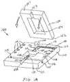
- FIG. 1Ais an exploded perspective view of an optical device package in accordance with the present description
- FIGS. 1B and 1Care plan views illustrating optical device packages with the optical fiber extending beyond lid
- FIG. 2is a perspective view of an optical fiber disposed within a ferrule
- FIGS. 3 and 4are exploded perspective views of alternative embodiments of the optical device package including a frame
- FIG. 5is a perspective view showing an alternative embodiment of the optical device package with an extended optical fiber and extended substrate
- FIGS. 6 and 7A and 7 Bare front elevational views illustrating the assembly of the optical device package
- FIGS. 8 , 9 and 10are perspective views showing an optical device package having optical fibers at opposite ends of the package
- FIG. 11is a front elevational view of an optical device package for flip mounting to a substrate
- FIG. 12is a front elevational view showing the optical device package of FIG. 11 mounted to a substrate;
- FIG. 13is a front elevational view of an alternative embodiment of a optical device package for flip mounting to a substrate.
- FIG. 14is a front elevational view of the optical device package of FIG. 13 mounted to a substrate.
- an optical device package 100includes a substrate 110 , an optical signal carrier such as optical fiber 130 , optionally an optical semiconductor component 140 with or without a lens 160 , and a lid 150 .
- Optical fiber 130is typically a relatively short stub having a length generally ranging from about 1 mm to about 5 mm.
- substrate 110can be any material suitable for providing an optical bench.
- a preferred material for fabricating substrate 110is silicon.
- Other suitable materialsinclude ceramic, polymers, and metal.
- Substrate 110has a proximal end 111 , a distal end 112 , and a horizontal upper major surface 116 .
- Substrate 110can be formed by etching and/or cutting or other suitable method to provide a reception means, i.e., longitudinally extending notch 113 for an optical signal carrier extending longitudinally for receiving the optical fiber 130 , and optionally a lateral groove 114 .
- the lateral groove 114can be formed by cutting the upper surface 116 with a dicing saw and is at least partially defined by proximal facing surface 115 .
- the notch 113is divided by the lateral groove 114 to form two separate notches, i.e., co-linear proximal notch 113 A and distal notch 113 B.
- the proximal end of proximal notch 113 Ais coterminous with the proximal end 111 of the substrate.
- the notch 113can have a V-shaped cross section and is typically referred to as a “V-groove,” although other cross sectional configurations such as U-shaped cross sections (semicircular, square, rectangular, etc.) are also contemplated.
- substrate 110is single crystal silicon with the upper major surface 116 being in the (100) crystallographic plane.
- the upper surface 116can be masked and selectively etched to form angled surfaces of the V-shaped notch 113 in the (111) crystallographic planes.
- Etchants capable of forming V-shaped groovesinclude potassium hydroxide, as is well known in the art.
- the depth of notch 113can be any suitable depth for accommodating the optical fiber 130 , and preferably ranges from about 50 microns to about 500 microns.
- Recess 118is optionally formed in the substrate. Likewise, a pocket 117 can be formed in which to mount a lens 117 for refracting the light beam traveling between the optical fiber 130 and the optical semiconductor component 140 .
- Optical fiber 130is positioned in distal section 113 B of the notch and can be any conventional optical fiber typically from about 1 mm to about 5 mm in length, although lengths outside of this range can also be employed when suitable.
- Optical fiber 130typically has a diameter of about 125 microns (standard). However, larger or smaller diameters can also be used when suitable.
- the optical fiber 130can be disposed through an axial bore 133 in a ferrule 131 , the ferrule 131 being disposed in proximal portion 113 B of the notch 113 .
- Ferrule 131is typically fabricated from ceramic or glass and generally can be from about 1 mm to 3 mm in diameter, although other diameters outside of this range can also be used.
- the optical semiconductor component 140is preferably mounted on the upper surface 116 of the substrate and can be any suitable semiconductor device for emitting or receiving light such as, for example, a laser diode, light emitting diode (LED), or a photodetector. Such optical semiconductor devices are well known in the art.
- Lid 150is can be fabricated from any suitable material such as silicon, glass, ceramic, metal, and the like. Lid 150 includes a recess 154 and a notch 153 for engaging an upper portion of the optical fiber 130 . Lid 150 can be mounted to the upper surface 116 of the substrate by means of a bonding agent such as adhesives such as epoxy resin, benzocyclobutene resin (BCB), or soldering agents such as solder metal or solder glass frit, and at least partially defines an interior space in which the optical semiconductor component 140 and lens 160 are enclosed.
- a bonding agentsuch as adhesives such as epoxy resin, benzocyclobutene resin (BCB), or soldering agents such as solder metal or solder glass frit
- Solder glass fritis a low melting point glass such as borate glass, lead zinc borate glass, and the like. Generally, solder glass frit can have a melting point of from about 300° C. to about 800° C., usually 325° C. to about 500° C. Solder glass frit suitable for use in the present invention is commercially available, for example, from Schott Glass Technologies of Duryea, Pa.
- the optical fiber 130can extend proximally beyond the proximal end 151 of the lid and over lateral groove 114 , preferably by a distance of from about 50 microns to about 400 microns. This provides the advantage that the bonding agent 50 does not wet the exposed proximal end face 132 of the optical fiber.
- the optical fiber 130can extend into the proximal notch 113 A.
- optical device package 100 Ais similar to embodiment 100 , except that a frame 120 is also employed, the frame 120 being mounted to the upper surface 116 of the substrate, and the lid 150 A being mounted to the frame. Lid 150 A does not require a recess to accommodate optical fiber 130 since this function is accomplished by the frame 120 .
- Frame 120is preferably a single piece band-like shaped member defining an opening 124 , and having a top surface 122 and a recess 123 configured and dimensioned to accommodate optical fiber 130 .
- Frame 120is an intermediate support structure preferably fabricated from a ceramic, glass, silicon, metal or other suitable material which does not plastically deform at the temperatures used to process and fabricate the present optical device package.
- Frame 120can be of any suitable dimensions and is preferably has a thickness D (see FIG. 6 ) ranging from about 100 microns to about 5 mm.
- Frame 120is fixedly bonded to the upper surface 116 of the substrate such that the optical semiconductor device 140 and at least a portion of the optical fiber 130 are at least partially disposed within the opening of the band-shaped frame 120 .
- Bonding of frame 120 to substrate 110can be achieved by any suitable means such as soldering with metal, bonding with solder glass frit or BCB or epoxy resins, etc.
- Upper surface 122 of frame 120can be metallized or roughened, if necessary, to facilitate soldering or bonding of the lid thereto.
- optical device package 100 Bis similar to optical device package 100 A except that the substrate 110 A, unlike substrate 110 , does not include a lateral groove equivalent to groove 114 in FIG. 3 .
- optical device package 100 Cis similar to optical device package 100 shown in FIG. 1A , except that substrate 110 A, unlike substrate 110 , does not include a lateral groove equivalent to groove 114 .
- the proximal end of notch 113is coterminous with the proximal end 111 of the substrate.
- the proximal end 111 of the substrateextends proximally beyond the proximal end 151 of the lid.
- proximal end 132 of the optical fiber 130extends proximally beyond the proximal end 151 of the lid by a distance of, for example, about 50 microns to about 500 microns, but is distally spaced apart from the proximal end 111 of the substrate.
- a substrate 110is provided with a V-shaped notch 113 configured and dimensioned to accommodate an optical fiber 130 (with or without ferrule 131 ).
- the exterior surface of the ferrule 131is coated with a layer of bonding agent such as solder glass 50 A. While the embodiment is described herein with reference to solder glass, it should be recognized that any suitable bond agent (examples given above) can be used instead of solder glass.
- the substrate and/or notch 113can be coated with solder glass.
- the frame 120includes a recess 123 for accommodating the ferrule 131 with the optical fiber.
- Recess 123can be of any suitable shape such as, e.g., hemispherical, V-shaped, U-shaped, rectangular, and the like.
- the bottom surface of the frame 120(or the upper surface of the substrate 110 ) is coated with a layer 50 B of solder glass.
- the optical fiber 130(with or without ferrule 131 ) is positioned within the V-shaped notch 113 and the frame is mounted to the substrate. Then the assembled frame 120 , optical fiber 130 (and optionally ferrule 131 ), and substrate 110 are heated to a temperature sufficient to fuse the solder glass, thereby fixedly bonding the frame 120 to the substrate 110 by means of a layer 50 of fused solder glass, as shown in FIG. 7A .
- layer 50 of fused solder glassfixedly secures the optical fiber 130 or ferrule 131 within V-shaped notch 113 and recess 123 .
- the optical semiconductor component or other internal componentscan then be mounted to the substrate 110 through the opening 124 of the frame (not shown).
- a lid 150 Acan be bonded to the upper surface of frame 120 by means of bonding agent 55 , which can be an adhesive, such as epoxy, or other bonding agent, including solder glass, which is capable of being cured, activated or fused at a temperature lower than that required for the step of securing the frame 120 to the substrate 110 .
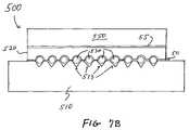
- FIG. 7Billustrates an optical device package 500 having a substrate 510 , frame 520 , and lid 550 .
- a layer of bonding agent 50is disposed between the frame 520 and the substrate 510 .
- a layer of bonding agent 55is disposed between the lid 550 and the frame 520 .
- Optical device package 500is similar to that illustrated in FIG. 7A except that multiple parallel spaced apart optical fibers 530 are disposed in respective multiple parallel notches 513 in the substrate.
- Optical semiconductor componentsare typically more sensitive to damage by heat than the optical fibers.
- use of a frame 120permits the optical fiber 130 to be secured at a relatively high temperature and the optical semiconductor component 140 to be subsequently secured to the substrate at a relatively lower temperature.
- bonding pads 170are disposed around the peripheral portion of the upper surface 116 of the substrate not covered by lid 150 . At least some of the bonding pads 170 are connected to the optical semiconductor component 140 by means of conductive electrical leads 171 .
- the optical semiconductor component 140is mounted to the ends 172 of leads 171 in the interior of the optical device package. Leads 171 extend under the lid 150 to the respective bonding pads 170 . Leads 171 are generally no thicker than the layer of the bonding agent (solder glass, adhesive, etc.) which secures the lid to the substrate.
- the frame 120can have recesses to accommodate the leads 171 .
- substrate 210includes an upper surface 216 , a recessed area 218 , a proximal end 211 and a distal end 212 .
- Substrate 210further includes a proximal V-shaped notch 213 A and a distal V-shaped notch 213 B.
- a first optical fiber stub 230 A(optionally disposed through a ferrule) is positioned in V-shaped notch 213 A.
- a second optical fiber stub 230 B(also optionally disposed through a ferrule) is positioned in V-shaped notch 213 B.
- a frame 220is fixedly mounted to the upper surface 216 of the substrate, e.g., by solder glass, epoxy resin, or other suitable bonding agent.
- Frame 220is preferably a single piece member having a band like structure which surrounds an opening, and proximal and distal recesses 223 A and 223 B, respectively, to accommodate the optical fibers 230 A and 230 B, respectively.
- the first and second optical fiber stubsmay optionally be co-linear or not co-linear.
- various optical devicessuch as lenses, filters, modulators, etc., can be positioned in the recessed area 218 of the substrate between the distal end of first optical fiber stub 230 A and the proximal end of second optical fiber stub 230 B.
- a lid(not shown) can optionally be fixedly mounted to the upper surface 221 of the frame.
- the proximal and distal ends of the optical fibers 230 A and 230 B, respectively,are flush with the proximal and distal ends, 211 and 212 , respectively, of the substrate.
- the substrate 210 Ahas a proximal end 211 A which extends proximally beyond the proximal end of the frame, and a distal end 212 A which extends distally beyond the distal end of the frame.
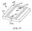
- substrate 251has a flat upper surface 254 without any recess corresponding to, e.g., recess 218 of FIGS. 8 and 9 .
- Optical fibers 261 and 262are positioned respectively in notches 252 and 253 .
- the optical axes of optical fibers 261 and 262are above the level of the upper surface 254 by any suitable distance, typically 5 microns to about 30 microns.
- Optical semiconductors, or other optical componentscan be mounted to the upper surface 254 within the area bounded by frame 270 .
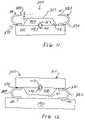
- an optical device package 300includes a substrate 310 having a notch 313 for the reception of optical fiber 330 .
- Lid 350is mounted to the substrate 310 and at least partially defines an interior space for enclosing various optical components such as optical semiconductor components, lenses, and the like.
- Bonding pads 370are disposed along the peripheral portion of the upper surface of the substrate which is not covered by the lid 350 .
- Legs 380are secured to respective bonding pads 370 .
- Legs 380are preferably U-shaped strips of conductive metal which provide flip mounting ability for the optical device package 300 .
- the top surface 381 of each leg 380is preferably at a level higher than the level of the top surface 351 of the lid 350 by a distance H, wherein H can be any suitable distance.
- Hcan range from about 25 microns to about 300 microns, more preferably from about 50 microns to about 200 microns.
- the top surface 381 of the legscan be from about 250 microns to about 1,000 microns above the upper surface 316 of the substrate 310 .
- legs 380are fabricated from a resilient metal so as to function as springs.
- the optical semiconductor componentis electrically connected to legs 380 by means of electrical leads, in a manner similar to the optical device package illustrated in FIGS.
- the electrically conductive leadsextend from the bonding pads 370 to the optical semiconductor component.
- the electrical leadsinclude thin films of conductive metal which are preferably no thicker than the layer of bonding agent (solder glass, epoxy resin, etc.) by which the lid 350 is bonded to the substrate 310 .
- bonding agentsolder glass, epoxy resin, etc.
- an optical device package 400includes a substrate 410 having a notch 413 for the reception of optical fiber 430 .
- Lid 450is mounted to the substrate 410 and at least partially defines an interior space for enclosing various optical components such as optical semiconductor components, lenses, and the like.
- Bonding pads 470are disposed along the peripheral portion of the upper surface of the substrate which is not covered by the lid 450 .
- Conductive metal legs 480are secured to respective bonding pads 370 .
- the metal legs 480can be electroformed or stamped copper or other metals such as gold, tin, silver, solder metal, and the like.
- the metal legs 480are shown in FIG. 9 as spheres. However, they can alternatively be cylindrical or of other shapes.
- each leg 480is higher than the top surface 451 of the lid to facilitate flip mounting of the optical device package 400 as discussed below.
- the legs 480can range in height of from about 250 microns to about 1,000 microns, although dimensions outside of this range can also be used when appropriate.
- the optical semiconductor componentis electrically connected to legs 480 by means of electrical leads, in a manner similar to the optical device package illustrated in FIGS. 1A and 3 .
- legs 480are contacted with corresponding electrical contacts (not shown) for incorporation into an electric circuit.
Landscapes
- Physics & Mathematics (AREA)
- General Physics & Mathematics (AREA)
- Optics & Photonics (AREA)
- Optical Couplings Of Light Guides (AREA)
Abstract
Description
Claims (22)
Priority Applications (2)
| Application Number | Priority Date | Filing Date | Title |
|---|---|---|---|
| US09/999,517US7345316B2 (en) | 2000-10-25 | 2001-10-24 | Wafer level packaging for optoelectronic devices |
| US11/503,023US8399897B2 (en) | 2000-10-25 | 2006-08-11 | Optical device package |
Applications Claiming Priority (2)
| Application Number | Priority Date | Filing Date | Title |
|---|---|---|---|
| US24317200P | 2000-10-25 | 2000-10-25 | |
| US09/999,517US7345316B2 (en) | 2000-10-25 | 2001-10-24 | Wafer level packaging for optoelectronic devices |
Related Child Applications (1)
| Application Number | Title | Priority Date | Filing Date |
|---|---|---|---|
| US11/503,023ContinuationUS8399897B2 (en) | 2000-10-25 | 2006-08-11 | Optical device package |
Publications (2)
| Publication Number | Publication Date |
|---|---|
| US20040264866A1 US20040264866A1 (en) | 2004-12-30 |
| US7345316B2true US7345316B2 (en) | 2008-03-18 |
Family
ID=33543795
Family Applications (2)
| Application Number | Title | Priority Date | Filing Date |
|---|---|---|---|
| US09/999,517Expired - Fee RelatedUS7345316B2 (en) | 2000-10-25 | 2001-10-24 | Wafer level packaging for optoelectronic devices |
| US11/503,023Expired - Fee RelatedUS8399897B2 (en) | 2000-10-25 | 2006-08-11 | Optical device package |
Family Applications After (1)
| Application Number | Title | Priority Date | Filing Date |
|---|---|---|---|
| US11/503,023Expired - Fee RelatedUS8399897B2 (en) | 2000-10-25 | 2006-08-11 | Optical device package |
Country Status (1)
| Country | Link |
|---|---|
| US (2) | US7345316B2 (en) |
Cited By (10)
| Publication number | Priority date | Publication date | Assignee | Title |
|---|---|---|---|---|
| US20090225636A1 (en)* | 2008-03-10 | 2009-09-10 | Toshiki Hirano | Components and assembly procedure for thermal assisted recording |
| US9206965B2 (en) | 2012-12-20 | 2015-12-08 | International Business Machines Corporation | Semiconductor photonic package |
| US9285542B2 (en)* | 2014-07-09 | 2016-03-15 | International Business Machines Corporation | Fiber optic interface with adhesive fill system |
| US9316796B2 (en) | 2013-03-14 | 2016-04-19 | International Business Machines Corporation | Fiber pigtail with integrated lid |
| US20160240306A1 (en)* | 2015-02-13 | 2016-08-18 | Murata Manufacturing Co., Ltd. | Coil component |
| US20160358832A1 (en)* | 2015-06-02 | 2016-12-08 | Ngk Spark Plug Co., Ltd. | Ceramic package and manufacturing method therefor |
| US9706670B1 (en) | 2015-12-31 | 2017-07-11 | International Business Machines Corporation | Connecting mid-board electronic devices |
| US9772458B1 (en)* | 2016-09-12 | 2017-09-26 | Yottahn, Inc. | Optical module for optical fibers and method of manufacturing the same |
| CN111128771A (en)* | 2019-12-19 | 2020-05-08 | 西北电子装备技术研究所(中国电子科技集团公司第二研究所) | Self-leveling and locking method for large-pressure flip bonding and adjusting platform of chip substrate |
| US11280968B2 (en) | 2020-02-21 | 2022-03-22 | International Business Machines Corporation | High-bandwidth embedded optical connector with latching mechanism |
Families Citing this family (27)
| Publication number | Priority date | Publication date | Assignee | Title |
|---|---|---|---|---|
| US6932519B2 (en)* | 2000-11-16 | 2005-08-23 | Shipley Company, L.L.C. | Optical device package |
| US7078671B1 (en)* | 2001-08-06 | 2006-07-18 | Shipley Company, L.L.C. | Silicon optical microbench devices and wafer-level testing thereof |
| US20040021214A1 (en)* | 2002-04-16 | 2004-02-05 | Avner Badehi | Electro-optic integrated circuits with connectors and methods for the production thereof |
| US7376312B2 (en)* | 2002-11-05 | 2008-05-20 | Rohm Co., Ltd. | Optical module and method for manufacturing the same |
| JP2004233484A (en)* | 2003-01-29 | 2004-08-19 | Oki Electric Ind Co Ltd | Optical module |
| EP1517166B1 (en) | 2003-09-15 | 2015-10-21 | Nuvotronics, LLC | Device package and methods for the fabrication and testing thereof |
| JP4258367B2 (en)* | 2003-12-18 | 2009-04-30 | 株式会社日立製作所 | Optical component mounting package and manufacturing method thereof |
| EP1677133A1 (en)* | 2004-12-30 | 2006-07-05 | Rohm and Haas Electronic Materials, L.L.C. | Microcomponent holder and method for manufacture thereof |
| US7267494B2 (en)* | 2005-02-01 | 2007-09-11 | Finisar Corporation | Fiber stub for cladding mode coupling reduction |
| US8050526B2 (en)* | 2005-02-08 | 2011-11-01 | Samsung Electronics Co., Ltd. | Micro-optical device and method of making same |
| TW200702762A (en)* | 2005-06-01 | 2007-01-16 | Rohm & Haas Elect Mat | Optical assemblies |
| CA2556117A1 (en)* | 2005-08-15 | 2007-02-15 | Rohm And Haas Electronic Materials Llc | Bonding methods and optical assemblies |
| KR100657971B1 (en)* | 2005-10-06 | 2006-12-14 | 삼성전자주식회사 | Optical Transmission Module and Thermal Auxiliary Magnetic Recording Head |
| EP1780565B1 (en)* | 2005-10-11 | 2014-01-01 | Samsung Electronics Co., Ltd. | Micro-optical device with a U-shaped type alignment waveguide |
| CN100586253C (en)* | 2005-11-09 | 2010-01-27 | 皇家飞利浦电子股份有限公司 | Packaging, packaging carrier and manufacturing method thereof, diagnostic device and manufacturing method thereof |
| JP5359272B2 (en)* | 2006-07-19 | 2013-12-04 | 株式会社ニコン | Optical fiber amplifier cassette, optical fiber amplifier, and light source device |
| US20090294949A1 (en)* | 2008-05-30 | 2009-12-03 | Infineon Technologies Ag | Molded semiconductor device |
| US8215850B2 (en)* | 2009-12-29 | 2012-07-10 | Prasad Yalamanchili | Optical module with fiber feedthrough |
| US20140127857A1 (en)* | 2012-11-07 | 2014-05-08 | Taiwan Semiconductor Manufacturing Company, Ltd. | Carrier Wafers, Methods of Manufacture Thereof, and Packaging Methods |
| US8916896B2 (en)* | 2013-02-22 | 2014-12-23 | Cree, Inc. | Light emitter components and methods having improved performance |
| CN104133271B (en)* | 2013-04-30 | 2017-06-16 | 赛恩倍吉科技顾问(深圳)有限公司 | Optical Fiber Transmission joint |
| US20150212267A1 (en)* | 2014-01-30 | 2015-07-30 | Tyco Electronics Nederland B.V. | Optical Assembly |
| US10319654B1 (en) | 2017-12-01 | 2019-06-11 | Cubic Corporation | Integrated chip scale packages |
| CN109116553B (en)* | 2018-10-10 | 2025-03-14 | 昂纳科技(深圳)集团股份有限公司 | Protective cover and protective structure |
| US11740418B2 (en) | 2021-03-23 | 2023-08-29 | Globalfoundries U.S. Inc. | Barrier structure with passage for waveguide in photonic integrated circuit |
| GB2607913A (en) | 2021-06-15 | 2022-12-21 | Rockley Photonics Ltd | Thermosonic bonding for securing photonic components |
| US12399325B2 (en)* | 2021-11-12 | 2025-08-26 | Cloud Light Technology Limited | Fiber to silicon photonics assembly method with fiber retaining apparatus |
Citations (89)
| Publication number | Priority date | Publication date | Assignee | Title |
|---|---|---|---|---|
| US3404215A (en) | 1966-04-14 | 1968-10-01 | Sprague Electric Co | Hermetically sealed electronic module |
| US3768991A (en) | 1972-06-14 | 1973-10-30 | Diacon | Method for sealing an enclosure for an electronic component |
| US3874549A (en) | 1972-05-26 | 1975-04-01 | Norman Hascoe | Hermetic sealing cover for a container for a semiconductor device |
| US4038157A (en) | 1976-04-16 | 1977-07-26 | The United States Of America As Represented By The Secretary Of The Air Force | Method of hermetically sealing semiconductor devices |
| US4065203A (en) | 1975-12-10 | 1977-12-27 | International Telephone And Telegraph Corporation | Couplers for electro-optical elements |
| US4199222A (en) | 1976-11-12 | 1980-04-22 | Hitachi, Ltd. | Optical device with a laser-to-fiber coupler |
| US4270134A (en) | 1978-04-28 | 1981-05-26 | Hitachi, Ltd. | Light-emitting semiconductor device |
| US4611884A (en) | 1982-11-24 | 1986-09-16 | Magnetic Controls Company | Bi-directional optical fiber coupler |
| US4639074A (en)* | 1984-06-18 | 1987-01-27 | At&T Bell Laboratories | Fiber-waveguide self alignment coupler |
| US4725114A (en)* | 1984-09-28 | 1988-02-16 | American Telephone And Telegraph Company, At&T Bell Laboratories | Optical waveguide lateral alignment arrangement |
| US4791075A (en) | 1987-10-05 | 1988-12-13 | Motorola, Inc. | Process for making a hermetic low cost pin grid array package |
| US4802952A (en) | 1987-03-06 | 1989-02-07 | Hitachi, Ltd. | Method for manufacturing semiconductor absolute pressure sensor units |
| US4818058A (en) | 1988-03-03 | 1989-04-04 | American Telephone And Telegraph Company At&T Bell Laboratories | Optical connector |
| US4826272A (en) | 1987-08-27 | 1989-05-02 | American Telephone And Telegraph Company At&T Bell Laboratories | Means for coupling an optical fiber to an opto-electronic device |
| US4897711A (en) | 1988-03-03 | 1990-01-30 | American Telephone And Telegraph Company | Subassembly for optoelectronic devices |
| US4904036A (en) | 1988-03-03 | 1990-02-27 | American Telephone And Telegraph Company, At&T Bell Laboratories | Subassemblies for optoelectronic hybrid integrated circuits |
| US4907065A (en) | 1988-03-01 | 1990-03-06 | Lsi Logic Corporation | Integrated circuit chip sealing assembly |
| US5071213A (en) | 1990-10-31 | 1991-12-10 | The Boeing Company | Optical coupler and method of making optical coupler |
| US5291572A (en) | 1993-01-14 | 1994-03-01 | At&T Bell Laboratories | Article comprising compression bonded parts |
| US5323051A (en) | 1991-12-16 | 1994-06-21 | Motorola, Inc. | Semiconductor wafer level package |
| US5384872A (en) | 1992-02-14 | 1995-01-24 | Lucas Industries Public Limited Company | Optical device and a method of manufacture thereof |
| US5412748A (en) | 1992-12-04 | 1995-05-02 | Kabushiki Kaisha Toshiba | Optical semiconductor module |
| US5436996A (en)* | 1990-07-11 | 1995-07-25 | Gte Laboratories Incorporated | Waferboard structure |
| US5448014A (en) | 1993-01-27 | 1995-09-05 | Trw Inc. | Mass simultaneous sealing and electrical connection of electronic devices |
| US5454055A (en) | 1992-09-29 | 1995-09-26 | Robert Bosch Gmbh | Method of making a cover for an integrated optical circuit, cover for an integrated optical circuit, and integrated optical circuit made with this cover |
| US5475778A (en) | 1993-10-21 | 1995-12-12 | Motorola, Inc. | Smart optical coupler and smart optical coupler system |
| US5497027A (en) | 1993-11-30 | 1996-03-05 | At&T Global Information Solutions Company | Multi-chip module packaging system |
| US5504372A (en) | 1992-08-21 | 1996-04-02 | Olin Corporation | Adhesively sealed metal electronic package incorporating a multi-chip module |
| US5550398A (en) | 1994-10-31 | 1996-08-27 | Texas Instruments Incorporated | Hermetic packaging with optical |
| US5557695A (en) | 1994-05-12 | 1996-09-17 | Fujitsu Limited | Waveguide-optical fiber connection structure and waveguide-optical fiber connection method |
| US5562837A (en) | 1994-02-10 | 1996-10-08 | Matra Marconi Space France | Method for connecting electronic circuits in a multi-chip module having a co-fired substrate and multi-chip module obtained thereby |
| US5604160A (en) | 1996-07-29 | 1997-02-18 | Motorola, Inc. | Method for packaging semiconductor devices |
| US5625733A (en) | 1995-02-09 | 1997-04-29 | Lucent Technologies Inc. | Arrangement for interconnecting an optical fiber to an optical component |
| US5631502A (en) | 1993-03-15 | 1997-05-20 | Kabushiki Kaisha Toshiba | Multi-chip module |
| US5635761A (en) | 1994-12-14 | 1997-06-03 | International Business Machines, Inc. | Internal resistor termination in multi-chip module environments |
| US5647042A (en)* | 1995-07-05 | 1997-07-08 | Fujitsu Limited | Optical link module connection system |
| US5656552A (en) | 1996-06-24 | 1997-08-12 | Hudak; John James | Method of making a thin conformal high-yielding multi-chip module |
| US5671315A (en) | 1994-03-09 | 1997-09-23 | Fujitsu Limited | Optical parts fixing apparatus and method of manufacturing the same |
| US5699073A (en) | 1996-03-04 | 1997-12-16 | Motorola | Integrated electro-optical package with carrier ring and method of fabrication |
| US5727104A (en)* | 1996-05-24 | 1998-03-10 | Fujitsu Limited | Optical transmission module and a method of producing the same |
| US5734555A (en) | 1994-03-30 | 1998-03-31 | Intel Corporation | Shared socket multi-chip module and/or piggyback pin grid array package |
| US5748822A (en)* | 1995-07-10 | 1998-05-05 | Fujitsu Limited | Optical module for connecting optical element and optical fiber |
| US5747870A (en) | 1994-06-30 | 1998-05-05 | Plessey Semiconductors Limited | Multi-chip module inductor structure |
| US5774614A (en) | 1996-07-16 | 1998-06-30 | Gilliland; Patrick B. | Optoelectronic coupling and method of making same |
| US5784780A (en) | 1995-10-04 | 1998-07-28 | Lsi Logic Corporation | Method of mounting a flip-chip |
| US5798557A (en) | 1996-08-29 | 1998-08-25 | Harris Corporation | Lid wafer bond packaging and micromachining |
| US5812571A (en) | 1996-10-25 | 1998-09-22 | W. L. Gore & Associates, Inc. | High-power vertical cavity surface emitting laser cluster |
| US5818404A (en) | 1996-03-04 | 1998-10-06 | Motorola, Inc. | Integrated electro-optical package |
| US5818699A (en) | 1995-07-05 | 1998-10-06 | Kabushiki Kaisha Toshiba | Multi-chip module and production method thereof |
| US5917976A (en) | 1997-04-23 | 1999-06-29 | Oki Electric Industry Co., Ltd. | Optical transmission path coupling method and optical transmission path coupling apparatus as well as optical axis self-alignment tool |
| US5933558A (en) | 1997-05-22 | 1999-08-03 | Motorola, Inc. | Optoelectronic device and method of assembly |
| US5949654A (en) | 1996-07-03 | 1999-09-07 | Kabushiki Kaisha Toshiba | Multi-chip module, an electronic device, and production method thereof |
| US5960141A (en) | 1997-10-17 | 1999-09-28 | Fujitsu Limited | Optical transmission terminal device |
| US6056448A (en) | 1998-04-16 | 2000-05-02 | Lockheed Martin Corporation | Vertical cavity surface emitting laser array packaging |
| US6061228A (en) | 1998-04-28 | 2000-05-09 | Harris Corporation | Multi-chip module having an integral capacitor element |
| US6074104A (en) | 1997-04-18 | 2000-06-13 | Nec Corporation | Method for hermetically sealing optical fiber introducing section and hermetically sealed structure |
| US6106735A (en) | 1997-01-11 | 2000-08-22 | Robert Bosch Gmbh | Wafer stack and method of producing sensors |
| US6112002A (en)* | 1996-11-29 | 2000-08-29 | Fujitsu Limited | Optical coupler optically coupling a light beam of a semiconductor laser source with a single mode optical waveguide or fiber |
| US6130979A (en) | 1997-07-14 | 2000-10-10 | Mitel Semiconductor Ab | Opto-electronic module |
| US6130444A (en)* | 1998-02-27 | 2000-10-10 | Nec Corporation | Optical fiber secured with a photosetting resin covered with a UV light-transmissive plate |
| US6165885A (en) | 1995-08-02 | 2000-12-26 | International Business Machines Corporation | Method of making components with solder balls |
| US6207950B1 (en) | 1999-01-11 | 2001-03-27 | Lightlogic, Inc. | Optical electronic assembly having a flexure for maintaining alignment between optical elements |
| US6221753B1 (en) | 1997-01-24 | 2001-04-24 | Micron Technology, Inc. | Flip chip technique for chip assembly |
| US6222967B1 (en) | 1997-03-13 | 2001-04-24 | Nippon Telegraph And Telephone Corporation | Packaging platform, optical module using the platform, and methods for producing the platform and the module |
| US6228675B1 (en) | 1999-07-23 | 2001-05-08 | Agilent Technologies, Inc. | Microcap wafer-level package with vias |
| US20010022382A1 (en) | 1998-07-29 | 2001-09-20 | Shook James Gill | Method of and apparatus for sealing an hermetic lid to a semiconductor die |
| US6293711B1 (en)* | 1998-03-18 | 2001-09-25 | Fujitsu Limited | Optical transmission module |
| US6309113B1 (en)* | 1998-04-02 | 2001-10-30 | Oki Electric Industry Co., Ltd. | Optical module, optical fiber connecting plug, and optical coupler equipped with the same |
| US6318909B1 (en) | 1999-02-11 | 2001-11-20 | Agilent Technologies, Inc. | Integrated packaging system for optical communications devices that provides automatic alignment with optical fibers |
| US6326680B1 (en)* | 1994-10-19 | 2001-12-04 | Telefonaktiebolaget Lm Ericsson (Publ) | Injection of encapsulating material on a optocomponent |
| US6377742B1 (en) | 1998-03-16 | 2002-04-23 | Sumitomo Electric Industries, Ltd. | Lead frame, optical module, and a method of optical module |
| US6376280B1 (en) | 1999-07-23 | 2002-04-23 | Agilent Technologies, Inc. | Microcap wafer-level package |
| US6400009B1 (en)* | 1999-10-15 | 2002-06-04 | Lucent Technologies Inc. | Hermatic firewall for MEMS packaging in flip-chip bonded geometry |
| US20020090749A1 (en) | 2001-01-09 | 2002-07-11 | 3M Innovative Properties Company | Hermetic package for mems devices with integrated carrier |
| US20020113296A1 (en) | 2001-02-03 | 2002-08-22 | Samsung Electronics Co., Ltd. | Wafer level hermetic sealing method |
| US6441481B1 (en) | 2000-04-10 | 2002-08-27 | Analog Devices, Inc. | Hermetically sealed microstructure package |
| US6452238B1 (en) | 1999-10-04 | 2002-09-17 | Texas Instruments Incorporated | MEMS wafer level package |
| US6513993B1 (en)* | 1999-09-28 | 2003-02-04 | Sumitomo Electric Industries, Ltd. | Optical communications device |
| US6521989B2 (en)* | 1998-10-08 | 2003-02-18 | Honeywell Inc. | Methods and apparatus for hermetically sealing electronic packages |
| US20030071283A1 (en) | 2001-10-17 | 2003-04-17 | Hymite A/S | Semiconductor structure with one or more through-holes |
| US20030081914A1 (en) | 2000-11-16 | 2003-05-01 | Steinberg Dan A. | Optical device package |
| US20030095759A1 (en) | 2000-12-14 | 2003-05-22 | Dautartas Mindaugas F. | Optical device package for flip-chip mounting |
| US20030123816A1 (en) | 2000-12-01 | 2003-07-03 | Steinberg Dan A. | Optical device package having a configured frame |
| US6611001B2 (en) | 2001-02-06 | 2003-08-26 | Lucent Technologies Inc. | Laser package |
| US6632027B1 (en)* | 1998-08-01 | 2003-10-14 | Hitachi, Ltd. | Optical module |
| US6635866B2 (en) | 2001-04-19 | 2003-10-21 | Internation Business Machines Corporation | Multi-functional fiber optic coupler |
| US6680491B2 (en) | 2000-02-01 | 2004-01-20 | Matsushita Electric Industrial Co., Ltd. | Optical electronic apparatus and method for producing the same |
| US20040012083A1 (en) | 2002-06-19 | 2004-01-22 | Brian Farrell | Electronic and optoelectronic component packaging technique |
| US6786654B2 (en)* | 2002-08-21 | 2004-09-07 | Hymite A/S | Encapsulated optical fiber end-coupled device |
Family Cites Families (6)
| Publication number | Priority date | Publication date | Assignee | Title |
|---|---|---|---|---|
| US4293826A (en)* | 1979-04-30 | 1981-10-06 | Xerox Corporation | Hybrid semiconductor laser/detectors |
| US5181216A (en)* | 1990-08-27 | 1993-01-19 | At&T Bell Laboratories | Photonics module apparatus |
| US5500540A (en)* | 1994-04-15 | 1996-03-19 | Photonics Research Incorporated | Wafer scale optoelectronic package |
| DE4431285C1 (en)* | 1994-09-02 | 1995-12-07 | Ant Nachrichtentech | Semiconductor laser module esp. for coupling into optical waveguide |
| DE19605726A1 (en) | 1996-02-16 | 1997-08-21 | Sel Alcatel Ag | Arrangement for optically coupling a monitor diode to a laser diode |
| US6516104B1 (en)* | 1999-06-25 | 2003-02-04 | Kabushiki Kaisha Toshiba | Optical wiring device |
- 2001
- 2001-10-24USUS09/999,517patent/US7345316B2/ennot_activeExpired - Fee Related
- 2006
- 2006-08-11USUS11/503,023patent/US8399897B2/ennot_activeExpired - Fee Related
Patent Citations (93)
| Publication number | Priority date | Publication date | Assignee | Title |
|---|---|---|---|---|
| US3404215A (en) | 1966-04-14 | 1968-10-01 | Sprague Electric Co | Hermetically sealed electronic module |
| US3874549A (en) | 1972-05-26 | 1975-04-01 | Norman Hascoe | Hermetic sealing cover for a container for a semiconductor device |
| US3768991A (en) | 1972-06-14 | 1973-10-30 | Diacon | Method for sealing an enclosure for an electronic component |
| US4065203A (en) | 1975-12-10 | 1977-12-27 | International Telephone And Telegraph Corporation | Couplers for electro-optical elements |
| US4038157A (en) | 1976-04-16 | 1977-07-26 | The United States Of America As Represented By The Secretary Of The Air Force | Method of hermetically sealing semiconductor devices |
| US4199222A (en) | 1976-11-12 | 1980-04-22 | Hitachi, Ltd. | Optical device with a laser-to-fiber coupler |
| US4270134A (en) | 1978-04-28 | 1981-05-26 | Hitachi, Ltd. | Light-emitting semiconductor device |
| US4611884A (en) | 1982-11-24 | 1986-09-16 | Magnetic Controls Company | Bi-directional optical fiber coupler |
| US4639074A (en)* | 1984-06-18 | 1987-01-27 | At&T Bell Laboratories | Fiber-waveguide self alignment coupler |
| US4725114A (en)* | 1984-09-28 | 1988-02-16 | American Telephone And Telegraph Company, At&T Bell Laboratories | Optical waveguide lateral alignment arrangement |
| US4802952A (en) | 1987-03-06 | 1989-02-07 | Hitachi, Ltd. | Method for manufacturing semiconductor absolute pressure sensor units |
| US4826272A (en) | 1987-08-27 | 1989-05-02 | American Telephone And Telegraph Company At&T Bell Laboratories | Means for coupling an optical fiber to an opto-electronic device |
| US4791075A (en) | 1987-10-05 | 1988-12-13 | Motorola, Inc. | Process for making a hermetic low cost pin grid array package |
| US4907065A (en) | 1988-03-01 | 1990-03-06 | Lsi Logic Corporation | Integrated circuit chip sealing assembly |
| US4897711A (en) | 1988-03-03 | 1990-01-30 | American Telephone And Telegraph Company | Subassembly for optoelectronic devices |
| US4904036A (en) | 1988-03-03 | 1990-02-27 | American Telephone And Telegraph Company, At&T Bell Laboratories | Subassemblies for optoelectronic hybrid integrated circuits |
| US4818058B1 (en) | 1988-03-03 | 1995-04-25 | Bell Telephone Labor Inc | Optical connector. |
| US4818058A (en) | 1988-03-03 | 1989-04-04 | American Telephone And Telegraph Company At&T Bell Laboratories | Optical connector |
| US5436996A (en)* | 1990-07-11 | 1995-07-25 | Gte Laboratories Incorporated | Waferboard structure |
| US5071213A (en) | 1990-10-31 | 1991-12-10 | The Boeing Company | Optical coupler and method of making optical coupler |
| US5323051A (en) | 1991-12-16 | 1994-06-21 | Motorola, Inc. | Semiconductor wafer level package |
| US5384872A (en) | 1992-02-14 | 1995-01-24 | Lucas Industries Public Limited Company | Optical device and a method of manufacture thereof |
| US5504372A (en) | 1992-08-21 | 1996-04-02 | Olin Corporation | Adhesively sealed metal electronic package incorporating a multi-chip module |
| US5454055A (en) | 1992-09-29 | 1995-09-26 | Robert Bosch Gmbh | Method of making a cover for an integrated optical circuit, cover for an integrated optical circuit, and integrated optical circuit made with this cover |
| US5412748A (en) | 1992-12-04 | 1995-05-02 | Kabushiki Kaisha Toshiba | Optical semiconductor module |
| US5291572A (en) | 1993-01-14 | 1994-03-01 | At&T Bell Laboratories | Article comprising compression bonded parts |
| US5448014A (en) | 1993-01-27 | 1995-09-05 | Trw Inc. | Mass simultaneous sealing and electrical connection of electronic devices |
| US5631502A (en) | 1993-03-15 | 1997-05-20 | Kabushiki Kaisha Toshiba | Multi-chip module |
| US5475778A (en) | 1993-10-21 | 1995-12-12 | Motorola, Inc. | Smart optical coupler and smart optical coupler system |
| US5497027A (en) | 1993-11-30 | 1996-03-05 | At&T Global Information Solutions Company | Multi-chip module packaging system |
| US5562837A (en) | 1994-02-10 | 1996-10-08 | Matra Marconi Space France | Method for connecting electronic circuits in a multi-chip module having a co-fired substrate and multi-chip module obtained thereby |
| US5671315A (en) | 1994-03-09 | 1997-09-23 | Fujitsu Limited | Optical parts fixing apparatus and method of manufacturing the same |
| US5734555A (en) | 1994-03-30 | 1998-03-31 | Intel Corporation | Shared socket multi-chip module and/or piggyback pin grid array package |
| US5557695A (en) | 1994-05-12 | 1996-09-17 | Fujitsu Limited | Waveguide-optical fiber connection structure and waveguide-optical fiber connection method |
| US5747870A (en) | 1994-06-30 | 1998-05-05 | Plessey Semiconductors Limited | Multi-chip module inductor structure |
| US6326680B1 (en)* | 1994-10-19 | 2001-12-04 | Telefonaktiebolaget Lm Ericsson (Publ) | Injection of encapsulating material on a optocomponent |
| US5550398A (en) | 1994-10-31 | 1996-08-27 | Texas Instruments Incorporated | Hermetic packaging with optical |
| US5635761A (en) | 1994-12-14 | 1997-06-03 | International Business Machines, Inc. | Internal resistor termination in multi-chip module environments |
| US5625733A (en) | 1995-02-09 | 1997-04-29 | Lucent Technologies Inc. | Arrangement for interconnecting an optical fiber to an optical component |
| US5818699A (en) | 1995-07-05 | 1998-10-06 | Kabushiki Kaisha Toshiba | Multi-chip module and production method thereof |
| US5647042A (en)* | 1995-07-05 | 1997-07-08 | Fujitsu Limited | Optical link module connection system |
| US5748822A (en)* | 1995-07-10 | 1998-05-05 | Fujitsu Limited | Optical module for connecting optical element and optical fiber |
| US5966488A (en)* | 1995-07-10 | 1999-10-12 | Fujitsu Limited | Optical module for connecting optical element and optical fiber |
| US6165885A (en) | 1995-08-02 | 2000-12-26 | International Business Machines Corporation | Method of making components with solder balls |
| US5784780A (en) | 1995-10-04 | 1998-07-28 | Lsi Logic Corporation | Method of mounting a flip-chip |
| US5699073A (en) | 1996-03-04 | 1997-12-16 | Motorola | Integrated electro-optical package with carrier ring and method of fabrication |
| US5818404A (en) | 1996-03-04 | 1998-10-06 | Motorola, Inc. | Integrated electro-optical package |
| US5727104A (en)* | 1996-05-24 | 1998-03-10 | Fujitsu Limited | Optical transmission module and a method of producing the same |
| US5656552A (en) | 1996-06-24 | 1997-08-12 | Hudak; John James | Method of making a thin conformal high-yielding multi-chip module |
| US5949654A (en) | 1996-07-03 | 1999-09-07 | Kabushiki Kaisha Toshiba | Multi-chip module, an electronic device, and production method thereof |
| US5774614A (en) | 1996-07-16 | 1998-06-30 | Gilliland; Patrick B. | Optoelectronic coupling and method of making same |
| US5604160A (en) | 1996-07-29 | 1997-02-18 | Motorola, Inc. | Method for packaging semiconductor devices |
| US5798557A (en) | 1996-08-29 | 1998-08-25 | Harris Corporation | Lid wafer bond packaging and micromachining |
| US5915168A (en) | 1996-08-29 | 1999-06-22 | Harris Corporation | Lid wafer bond packaging and micromachining |
| US5812571A (en) | 1996-10-25 | 1998-09-22 | W. L. Gore & Associates, Inc. | High-power vertical cavity surface emitting laser cluster |
| US6112002A (en)* | 1996-11-29 | 2000-08-29 | Fujitsu Limited | Optical coupler optically coupling a light beam of a semiconductor laser source with a single mode optical waveguide or fiber |
| US6106735A (en) | 1997-01-11 | 2000-08-22 | Robert Bosch Gmbh | Wafer stack and method of producing sensors |
| US6221753B1 (en) | 1997-01-24 | 2001-04-24 | Micron Technology, Inc. | Flip chip technique for chip assembly |
| US6222967B1 (en) | 1997-03-13 | 2001-04-24 | Nippon Telegraph And Telephone Corporation | Packaging platform, optical module using the platform, and methods for producing the platform and the module |
| US6318910B1 (en) | 1997-04-18 | 2001-11-20 | Nec Corporation | Method for hermetically sealing optical fiber introducing section and hermetically sealed structure |
| US6074104A (en) | 1997-04-18 | 2000-06-13 | Nec Corporation | Method for hermetically sealing optical fiber introducing section and hermetically sealed structure |
| US5917976A (en) | 1997-04-23 | 1999-06-29 | Oki Electric Industry Co., Ltd. | Optical transmission path coupling method and optical transmission path coupling apparatus as well as optical axis self-alignment tool |
| US5933558A (en) | 1997-05-22 | 1999-08-03 | Motorola, Inc. | Optoelectronic device and method of assembly |
| US6130979A (en) | 1997-07-14 | 2000-10-10 | Mitel Semiconductor Ab | Opto-electronic module |
| US5960141A (en) | 1997-10-17 | 1999-09-28 | Fujitsu Limited | Optical transmission terminal device |
| US6130444A (en)* | 1998-02-27 | 2000-10-10 | Nec Corporation | Optical fiber secured with a photosetting resin covered with a UV light-transmissive plate |
| US6377742B1 (en) | 1998-03-16 | 2002-04-23 | Sumitomo Electric Industries, Ltd. | Lead frame, optical module, and a method of optical module |
| US6293711B1 (en)* | 1998-03-18 | 2001-09-25 | Fujitsu Limited | Optical transmission module |
| US6309113B1 (en)* | 1998-04-02 | 2001-10-30 | Oki Electric Industry Co., Ltd. | Optical module, optical fiber connecting plug, and optical coupler equipped with the same |
| US6056448A (en) | 1998-04-16 | 2000-05-02 | Lockheed Martin Corporation | Vertical cavity surface emitting laser array packaging |
| US6061228A (en) | 1998-04-28 | 2000-05-09 | Harris Corporation | Multi-chip module having an integral capacitor element |
| US20010022382A1 (en) | 1998-07-29 | 2001-09-20 | Shook James Gill | Method of and apparatus for sealing an hermetic lid to a semiconductor die |
| US6632027B1 (en)* | 1998-08-01 | 2003-10-14 | Hitachi, Ltd. | Optical module |
| US6521989B2 (en)* | 1998-10-08 | 2003-02-18 | Honeywell Inc. | Methods and apparatus for hermetically sealing electronic packages |
| US6207950B1 (en) | 1999-01-11 | 2001-03-27 | Lightlogic, Inc. | Optical electronic assembly having a flexure for maintaining alignment between optical elements |
| US6318909B1 (en) | 1999-02-11 | 2001-11-20 | Agilent Technologies, Inc. | Integrated packaging system for optical communications devices that provides automatic alignment with optical fibers |
| US6376280B1 (en) | 1999-07-23 | 2002-04-23 | Agilent Technologies, Inc. | Microcap wafer-level package |
| US6228675B1 (en) | 1999-07-23 | 2001-05-08 | Agilent Technologies, Inc. | Microcap wafer-level package with vias |
| US6513993B1 (en)* | 1999-09-28 | 2003-02-04 | Sumitomo Electric Industries, Ltd. | Optical communications device |
| US6452238B1 (en) | 1999-10-04 | 2002-09-17 | Texas Instruments Incorporated | MEMS wafer level package |
| US6400009B1 (en)* | 1999-10-15 | 2002-06-04 | Lucent Technologies Inc. | Hermatic firewall for MEMS packaging in flip-chip bonded geometry |
| US6680491B2 (en) | 2000-02-01 | 2004-01-20 | Matsushita Electric Industrial Co., Ltd. | Optical electronic apparatus and method for producing the same |
| US6441481B1 (en) | 2000-04-10 | 2002-08-27 | Analog Devices, Inc. | Hermetically sealed microstructure package |
| US20030081914A1 (en) | 2000-11-16 | 2003-05-01 | Steinberg Dan A. | Optical device package |
| US20030123816A1 (en) | 2000-12-01 | 2003-07-03 | Steinberg Dan A. | Optical device package having a configured frame |
| US20030095759A1 (en) | 2000-12-14 | 2003-05-22 | Dautartas Mindaugas F. | Optical device package for flip-chip mounting |
| US20020090749A1 (en) | 2001-01-09 | 2002-07-11 | 3M Innovative Properties Company | Hermetic package for mems devices with integrated carrier |
| US20020113296A1 (en) | 2001-02-03 | 2002-08-22 | Samsung Electronics Co., Ltd. | Wafer level hermetic sealing method |
| US6611001B2 (en) | 2001-02-06 | 2003-08-26 | Lucent Technologies Inc. | Laser package |
| US6635866B2 (en) | 2001-04-19 | 2003-10-21 | Internation Business Machines Corporation | Multi-functional fiber optic coupler |
| US20030071283A1 (en) | 2001-10-17 | 2003-04-17 | Hymite A/S | Semiconductor structure with one or more through-holes |
| US20040012083A1 (en) | 2002-06-19 | 2004-01-22 | Brian Farrell | Electronic and optoelectronic component packaging technique |
| US6786654B2 (en)* | 2002-08-21 | 2004-09-07 | Hymite A/S | Encapsulated optical fiber end-coupled device |
Cited By (15)
| Publication number | Priority date | Publication date | Assignee | Title |
|---|---|---|---|---|
| US20090225636A1 (en)* | 2008-03-10 | 2009-09-10 | Toshiki Hirano | Components and assembly procedure for thermal assisted recording |
| US7986592B2 (en)* | 2008-03-10 | 2011-07-26 | Hitachi Global Storage Technologies, Netherlands B.V. | Components and assembly procedure for thermal assisted recording |
| US9206965B2 (en) | 2012-12-20 | 2015-12-08 | International Business Machines Corporation | Semiconductor photonic package |
| US9243784B2 (en) | 2012-12-20 | 2016-01-26 | International Business Machines Corporation | Semiconductor photonic package |
| US9400356B2 (en) | 2013-03-14 | 2016-07-26 | International Business Machines Corporation | Fiber pigtail with integrated lid |
| US9316796B2 (en) | 2013-03-14 | 2016-04-19 | International Business Machines Corporation | Fiber pigtail with integrated lid |
| US9285542B2 (en)* | 2014-07-09 | 2016-03-15 | International Business Machines Corporation | Fiber optic interface with adhesive fill system |
| US20160240306A1 (en)* | 2015-02-13 | 2016-08-18 | Murata Manufacturing Co., Ltd. | Coil component |
| US10347415B2 (en)* | 2015-02-13 | 2019-07-09 | Murata Manufacturing Co., Ltd. | Coil component |
| US20160358832A1 (en)* | 2015-06-02 | 2016-12-08 | Ngk Spark Plug Co., Ltd. | Ceramic package and manufacturing method therefor |
| US10014189B2 (en)* | 2015-06-02 | 2018-07-03 | Ngk Spark Plug Co., Ltd. | Ceramic package with brazing material near seal member |
| US9706670B1 (en) | 2015-12-31 | 2017-07-11 | International Business Machines Corporation | Connecting mid-board electronic devices |
| US9772458B1 (en)* | 2016-09-12 | 2017-09-26 | Yottahn, Inc. | Optical module for optical fibers and method of manufacturing the same |
| CN111128771A (en)* | 2019-12-19 | 2020-05-08 | 西北电子装备技术研究所(中国电子科技集团公司第二研究所) | Self-leveling and locking method for large-pressure flip bonding and adjusting platform of chip substrate |
| US11280968B2 (en) | 2020-02-21 | 2022-03-22 | International Business Machines Corporation | High-bandwidth embedded optical connector with latching mechanism |
Also Published As
| Publication number | Publication date |
|---|---|
| US8399897B2 (en) | 2013-03-19 |
| US20060284294A1 (en) | 2006-12-21 |
| US20040264866A1 (en) | 2004-12-30 |
Similar Documents
| Publication | Publication Date | Title |
|---|---|---|
| US7345316B2 (en) | Wafer level packaging for optoelectronic devices | |
| US6932519B2 (en) | Optical device package | |
| US6883977B2 (en) | Optical device package for flip-chip mounting | |
| JP3778549B2 (en) | Airtight chip scale package for photon devices | |
| US6686588B1 (en) | Optical module with lens integral holder | |
| US6900509B2 (en) | Optical receiver package | |
| KR920003708B1 (en) | Subassemblies for Optoelectronic Devices | |
| US7609461B1 (en) | Optical module having cavity substrate | |
| US7138661B2 (en) | Optoelectronic component and optoelectronic arrangement with an optoelectronic component | |
| US7961989B2 (en) | Optical chassis, camera having an optical chassis, and associated methods | |
| US20060110110A1 (en) | Optical turn system for optoelectronic modules | |
| JPS63102379A (en) | Photocoupler or reflected light barrier and manufacture of the same | |
| TW201436294A (en) | Optoelectronic device with laminated leadless carrier package oriented in lateral or topographical orientation (1) | |
| US6827503B2 (en) | Optical device package having a configured frame | |
| US7520679B2 (en) | Optical device package with turning mirror and alignment post | |
| TWI233509B (en) | Optoelectronic package structure and process for planar passive optical and optoelectronic devices | |
| JPS60180183A (en) | Hermetically sealing package for optical semiconductor element | |
| JP4728625B2 (en) | Optical semiconductor device and optical module using the same | |
| JP3717623B2 (en) | Optoelectronic device and manufacturing method thereof | |
| JP4038669B2 (en) | Optical receiver and manufacturing method thereof | |
| EP0118554B1 (en) | Optical device | |
| JPH10213723A (en) | Optical semiconductor module and manufacturing method thereof | |
| EP1953577B1 (en) | Package for optoelectronic device on wafer level | |
| JPH04212905A (en) | optical semiconductor module | |
| JPH10153724A (en) | Photosemiconductor module |
Legal Events
| Date | Code | Title | Description |
|---|---|---|---|
| AS | Assignment | Owner name:HALEOS, INC., VIRGINIA Free format text:ASSIGNMENT OF ASSIGNORS INTEREST;ASSIGNORS:STEINBERG, DAN A.;HUGHES, WILLIAM T.;DAUTARTAS, MINDAUGAS F.;AND OTHERS;REEL/FRAME:013174/0328;SIGNING DATES FROM 20020910 TO 20020920 Owner name:SHIPLEY COMPANY, L.L.C., MASSACHUSETTS Free format text:ASSIGNMENT OF ASSIGNORS INTEREST;ASSIGNOR:HALEOS, INC.;REEL/FRAME:013181/0159 Effective date:20020911 Owner name:HALEOS, INC., VIRGINIA Free format text:ASSIGNMENT OF ASSIGNORS INTEREST;ASSIGNORS:STEINBERG, DAN A.;HUGHES, WILLIAM T.;DAUTARTAS, MINDAUGAS F.;AND OTHERS;SIGNING DATES FROM 20020910 TO 20020920;REEL/FRAME:013174/0328 | |
| STCF | Information on status: patent grant | Free format text:PATENTED CASE | |
| AS | Assignment | Owner name:ROHM AND HAAS ELECTRONIC MATERIALS LLC, MARYLAND Free format text:CHANGE OF NAME;ASSIGNOR:SHIPLEY COMPANY, L.L.C.;REEL/FRAME:022542/0113 Effective date:20040119 Owner name:NUVOTRONICS, LLC, VIRGINIA Free format text:ASSIGNMENT OF ASSIGNORS INTEREST;ASSIGNOR:ROHM AND HAAS ELECTRONIC MATERIALS LLC;REEL/FRAME:022542/0125 Effective date:20080708 | |
| FEPP | Fee payment procedure | Free format text:PAYOR NUMBER ASSIGNED (ORIGINAL EVENT CODE: ASPN); ENTITY STATUS OF PATENT OWNER: LARGE ENTITY Free format text:PAYER NUMBER DE-ASSIGNED (ORIGINAL EVENT CODE: RMPN); ENTITY STATUS OF PATENT OWNER: LARGE ENTITY | |
| AS | Assignment | Owner name:IP CUBE PARTNERS CO. LTD., KOREA, REPUBLIC OF Free format text:ASSIGNMENT OF ASSIGNORS INTEREST;ASSIGNOR:NUVOTRONICS, LLC;REEL/FRAME:025955/0330 Effective date:20100831 | |
| AS | Assignment | Owner name:SAMSUNG ELECTRONICS CO., LTD., KOREA, REPUBLIC OF Free format text:ASSIGNMENT OF ASSIGNORS INTEREST;ASSIGNOR:IP CUBE PARTNERS CO. LTD.;REEL/FRAME:026323/0651 Effective date:20110512 | |
| FPAY | Fee payment | Year of fee payment:4 | |
| FPAY | Fee payment | Year of fee payment:8 | |
| FEPP | Fee payment procedure | Free format text:MAINTENANCE FEE REMINDER MAILED (ORIGINAL EVENT CODE: REM.); ENTITY STATUS OF PATENT OWNER: LARGE ENTITY | |
| LAPS | Lapse for failure to pay maintenance fees | Free format text:PATENT EXPIRED FOR FAILURE TO PAY MAINTENANCE FEES (ORIGINAL EVENT CODE: EXP.); ENTITY STATUS OF PATENT OWNER: LARGE ENTITY | |
| STCH | Information on status: patent discontinuation | Free format text:PATENT EXPIRED DUE TO NONPAYMENT OF MAINTENANCE FEES UNDER 37 CFR 1.362 | |
| FP | Lapsed due to failure to pay maintenance fee | Effective date:20200318 |