US7342981B2 - Digital receiver having adaptive carrier recovery circuit - Google Patents
Digital receiver having adaptive carrier recovery circuitDownload PDFInfo
- Publication number
- US7342981B2 US7342981B2US10/757,536US75753604AUS7342981B2US 7342981 B2US7342981 B2US 7342981B2US 75753604 AUS75753604 AUS 75753604AUS 7342981 B2US7342981 B2US 7342981B2
- Authority
- US
- United States
- Prior art keywords
- signal
- phase
- receiver
- phase error
- estimate
- Prior art date
- Legal status (The legal status is an assumption and is not a legal conclusion. Google has not performed a legal analysis and makes no representation as to the accuracy of the status listed.)
- Expired - Fee Related, expires
Links
Images


Classifications
- H—ELECTRICITY
- H04—ELECTRIC COMMUNICATION TECHNIQUE
- H04L—TRANSMISSION OF DIGITAL INFORMATION, e.g. TELEGRAPHIC COMMUNICATION
- H04L25/00—Baseband systems
- H04L25/02—Details ; arrangements for supplying electrical power along data transmission lines
- H04L25/03—Shaping networks in transmitter or receiver, e.g. adaptive shaping networks
- H04L25/03006—Arrangements for removing intersymbol interference
- H04L25/03012—Arrangements for removing intersymbol interference operating in the time domain
- H04L25/03019—Arrangements for removing intersymbol interference operating in the time domain adaptive, i.e. capable of adjustment during data reception
- H04L25/03057—Arrangements for removing intersymbol interference operating in the time domain adaptive, i.e. capable of adjustment during data reception with a recursive structure
- H04L25/0307—Arrangements for removing intersymbol interference operating in the time domain adaptive, i.e. capable of adjustment during data reception with a recursive structure using blind adaptation
- H—ELECTRICITY
- H04—ELECTRIC COMMUNICATION TECHNIQUE
- H04L—TRANSMISSION OF DIGITAL INFORMATION, e.g. TELEGRAPHIC COMMUNICATION
- H04L27/00—Modulated-carrier systems
- H04L27/02—Amplitude-modulated carrier systems, e.g. using on-off keying; Single sideband or vestigial sideband modulation
- H04L27/06—Demodulator circuits; Receiver circuits
- H04L27/066—Carrier recovery circuits
- H—ELECTRICITY
- H04—ELECTRIC COMMUNICATION TECHNIQUE
- H04L—TRANSMISSION OF DIGITAL INFORMATION, e.g. TELEGRAPHIC COMMUNICATION
- H04L25/00—Baseband systems
- H04L25/02—Details ; arrangements for supplying electrical power along data transmission lines
- H04L25/03—Shaping networks in transmitter or receiver, e.g. adaptive shaping networks
- H04L25/03006—Arrangements for removing intersymbol interference
- H04L2025/0335—Arrangements for removing intersymbol interference characterised by the type of transmission
- H04L2025/03375—Passband transmission
- H04L2025/03382—Single of vestigal sideband
- H—ELECTRICITY
- H04—ELECTRIC COMMUNICATION TECHNIQUE
- H04L—TRANSMISSION OF DIGITAL INFORMATION, e.g. TELEGRAPHIC COMMUNICATION
- H04L25/00—Baseband systems
- H04L25/02—Details ; arrangements for supplying electrical power along data transmission lines
- H04L25/03—Shaping networks in transmitter or receiver, e.g. adaptive shaping networks
- H04L25/03006—Arrangements for removing intersymbol interference
- H04L2025/0335—Arrangements for removing intersymbol interference characterised by the type of transmission
- H04L2025/03375—Passband transmission
- H04L2025/0342—QAM
- H—ELECTRICITY
- H04—ELECTRIC COMMUNICATION TECHNIQUE
- H04L—TRANSMISSION OF DIGITAL INFORMATION, e.g. TELEGRAPHIC COMMUNICATION
- H04L25/00—Baseband systems
- H04L25/02—Details ; arrangements for supplying electrical power along data transmission lines
- H04L25/03—Shaping networks in transmitter or receiver, e.g. adaptive shaping networks
- H04L25/03006—Arrangements for removing intersymbol interference
- H04L2025/03433—Arrangements for removing intersymbol interference characterised by equaliser structure
- H04L2025/03439—Fixed structures
- H04L2025/03445—Time domain
- H04L2025/03471—Tapped delay lines
- H04L2025/03484—Tapped delay lines time-recursive
- H04L2025/0349—Tapped delay lines time-recursive as a feedback filter
- H—ELECTRICITY
- H04—ELECTRIC COMMUNICATION TECHNIQUE
- H04L—TRANSMISSION OF DIGITAL INFORMATION, e.g. TELEGRAPHIC COMMUNICATION
- H04L25/00—Baseband systems
- H04L25/02—Details ; arrangements for supplying electrical power along data transmission lines
- H04L25/03—Shaping networks in transmitter or receiver, e.g. adaptive shaping networks
- H04L25/03006—Arrangements for removing intersymbol interference
- H04L2025/03592—Adaptation methods
- H04L2025/03598—Algorithms
- H04L2025/03611—Iterative algorithms
- H04L2025/03617—Time recursive algorithms
- H04L2025/0363—Feature restoration, e.g. constant modulus
- H—ELECTRICITY
- H04—ELECTRIC COMMUNICATION TECHNIQUE
- H04L—TRANSMISSION OF DIGITAL INFORMATION, e.g. TELEGRAPHIC COMMUNICATION
- H04L27/00—Modulated-carrier systems
- H04L27/0014—Carrier regulation
- H04L2027/0024—Carrier regulation at the receiver end
- H04L2027/0026—Correction of carrier offset
- H04L2027/003—Correction of carrier offset at baseband only
- H—ELECTRICITY
- H04—ELECTRIC COMMUNICATION TECHNIQUE
- H04L—TRANSMISSION OF DIGITAL INFORMATION, e.g. TELEGRAPHIC COMMUNICATION
- H04L27/00—Modulated-carrier systems
- H04L27/0014—Carrier regulation
- H04L2027/0024—Carrier regulation at the receiver end
- H04L2027/0026—Correction of carrier offset
- H04L2027/0038—Correction of carrier offset using an equaliser
- H—ELECTRICITY
- H04—ELECTRIC COMMUNICATION TECHNIQUE
- H04L—TRANSMISSION OF DIGITAL INFORMATION, e.g. TELEGRAPHIC COMMUNICATION
- H04L27/00—Modulated-carrier systems
- H04L27/0014—Carrier regulation
- H04L2027/0044—Control loops for carrier regulation
- H04L2027/0063—Elements of loops
- H04L2027/0067—Phase error detectors
- H—ELECTRICITY
- H04—ELECTRIC COMMUNICATION TECHNIQUE
- H04L—TRANSMISSION OF DIGITAL INFORMATION, e.g. TELEGRAPHIC COMMUNICATION
- H04L27/00—Modulated-carrier systems
- H04L27/0014—Carrier regulation
- H04L2027/0044—Control loops for carrier regulation
- H04L2027/0063—Elements of loops
- H04L2027/0069—Loop filters
- H—ELECTRICITY
- H04—ELECTRIC COMMUNICATION TECHNIQUE
- H04L—TRANSMISSION OF DIGITAL INFORMATION, e.g. TELEGRAPHIC COMMUNICATION
- H04L27/00—Modulated-carrier systems
- H04L27/0014—Carrier regulation
- H04L2027/0044—Control loops for carrier regulation
- H04L2027/0071—Control of loops
Definitions
- the present inventionrelates generally to digital signal receivers and more particularly to a receiver including an adaptive carrier recovery circuit and methods for such receivers.
- digital transmittersmodulate digital information onto radio frequency carrier signals.
- the modulated information signalsare propagated to digital signal receivers where the digital signals may be demodulated and decoded.
- quadrature amplitude modulationas detailed in International Telecommunications Union (ITU) recommendation ITU-T J.83B/SCTE DVS-031/DOCSIS
- VSBvestigial side-band modulation
- ATSCAdvanced Television Standard Committee
- propagation media for the signalsintroduce distortions in signals received at the receiver.
- Distortionsmay, for example, be introduced as a result of noise, phase shifts, signal attenuation, and multi-path interference.
- Imperfections at the transmittermay similarly introduce distortions in the transmitted signal.
- these distortionsmay manifest themselves as increased bit errors in the decoded digital signal at the receiver.
- the digital signalsmay include forward error correcting (FEC) codes.
- FECforward error correcting
- One or more equalizersmay be used at the receiver to compensate for phase and amplitude distortions introduced into the transmitted signal by the propagation medium, such as multipath distortion.
- any equalizer at the receiveris typically adaptive and allows its parameters to be matched to the propagation medium at the receiver.
- the equalizershould also be able to compensate for variations in the propagation medium over time.
- a conventional digital receivermay include a feed forward equalizer (FFE), a decision feedback equalizer (DFE), and a carrier recovery circuit, each designed to compensate for distortion in the received signal.
- FFEfeed forward equalizer
- DFEdecision feedback equalizer
- carrier recovery circuiteach designed to compensate for distortion in the received signal.
- the FFE and DFEminimize multipath inter-symbol interference. Specifically, the FFE mitigates the effect of delayed echo multipath distortion (“pre-cursor”), while the DFE minimizes leading (“post cursor”) multipath interference. Error metrics between the demodulated signal and the reconstructed signal are used to provide closed loop adjustment of equalizer parameters.
- the carrier recovery circuitcompensates for shifts in phase and/or of the carrier frequency of the broadcasted signal. The aim is to adjust simultaneously FFE and DFE equalizer and carrier recovery circuit parameters to compensate for the propagation medium distortion.
- a blind equalization techniqueusing for example, the Constant Modulus Algorithm (CMA), may be used to adjust equalizer parameters.
- CMAConstant Modulus Algorithm
- the disclosed receivermay not be able to track fast changes in the carrier frequency or phase. This is particularly acute when the receiver is used to receive VSB modulated signals, which are highly carrier dependent. Indeed, for VSB signals phase distortion affects real and complex values of the VSB constellation differently. Furthermore, a CMA will not be phase independent when applied to a signal modulated with a VSB constellation, as it is with a QAM modulation for example.
- a digital receiverincludes an adaptive fine carrier recovery circuit that compensates for deviations in the carrier frequency or phase.
- the fine carrier recovery circuitde-rotates a signal including phase errors.
- Estimations of phase errorsare filtered using a filter whose gain and bandwidth are adjusted adaptively. This allows the carrier recovery circuit to track phase/frequency offset without introducing significant jitter.
- the receiverincludes a DFE, and the adaptive carrier recovery circuit mitigates instability that might be associated with the DFE.
- a digital receiverfor demodulating a digital signal modulated onto a carrier, includes a tuner; an analog to digital converter, for digitizing a channel tuned by the tuner to provide a digitized channel; a coarse carrier recovery circuit for extracting the signal from the digitized channel at near baseband; a feed forward equalizer receiving the signal at near baseband and outputting a feed forward equalized signal; a fine carrier recovery circuit for phase shifting the feed forward equalized signal by a phase correction angle to adjust for remaining offsets in phase and frequency of the feed forward equalized signal attributable to phase and frequency offsets in the carrier.
- the fine carrier recovery circuitincludes a filter for filtering an estimate of a phase error in the carrier to control the phase correction angle. At least one filter parameter of the filter varies adaptively with the phase error.
- a methodin a digital receiver for receiving a signal modulated onto a carrier, includes reducing multi-path interference in the signal, by filtering the signal through a feed-forward equalizer to produce a feed forward-equalized signal; determining an estimate of a remaining phase error in the carrier; filtering the estimate through a filter having at least one adjustable filter parameter to produce a phase correction signal; varying the adjustable parameter with the estimate of phase error; and multiplying the feed forward equalized signal by the phase correction signal to de-rotate the feed forward equalized signal.
- a digital receiverfor demodulating a digital signal modulated onto a carrier, to produce a demodulated digital signal.
- the receiverincludes a de-rotator for phase shifting an equalized version of the digital signal by a phase correction angle to adjust for remaining offsets in phase and frequency of the equalized version of the digital signal attributable to phase and frequency offsets in the carrier, and a filter in communication with the de-rotator, for filtering an estimate of a phase error in the demodulated digital signal to control the phase correction angle. At least one filter parameter of the filter varies adaptively with the phase error.
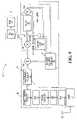
- FIG. 1is a simplified schematic block diagram of a VSB receiver exemplary of an embodiment of the present invention
- FIG. 2is a simplified schematic block diagram of a carrier loop of the receiver of FIG. 1 ;
- FIG. 3A-3E , 4 A- 4 B and 5 A- 5 Bare simplified block diagrams of portions of a phase error detector of the carrier loop of FIG. 2 ;
- FIG. 6is a simplified schematic block diagram of an adaptive loop filter of the carrier loop of FIG. 2 ;
- FIG. 7is a simplified schematic block diagram of an adaptive gain circuit of the carrier loop of FIG. 2 ;
- FIG. 8is a simplified schematic block diagram of a low pass filter of the carrier loop of FIG. 2 ;
- FIG. 9is a simplified schematic block diagram of a QAM receiver exemplary of an embodiment of the present invention.
- FIG. 1illustrates a VSB receiver 10 , including a carrier recovery circuit 29 , exemplary of an embodiment of the present invention.
- VSB receiver 10may for example be used to receive a digital television signal, as specified by the Advanced Television Systems Committee (ATSC) in the standard A53/B.
- Receiver 10may be formed as an integrated circuit using conventional application specific integrated circuit manufacturing techniques.
- Receiver 10is interconnected to an antenna 12 , providing a radio frequency signal to a tuner 14 .
- Tuner 14selects a tuned ATSC digital 6 Mhz wide channel of interest at an assumed frequency in a conventional manner.
- Tuner 14translates the tuned channel to an intermediate frequency (IF) so that all channels can be processed at a single unique frequency by the receiver front end 16 .
- Front end 16scales the received channel by automatic gain control amplifier 17 to allow the channel to be digitized by analog to digital (A/D) converter 18 .
- A/D converter 18samples the analog channel at the IF frequency and provides a digital signal corresponding to the digitized channel at second IF frequency.
- the digitized channelis passed to timing recovery block 20 where timing information is extracted, in a manner understood by those of ordinary skill.
- the timing informationestablishes the clock rate and phase at which symbols forming the signal of interest modulated on the carrier are detected.
- the digitized channelis optionally amplified by automatic gain control (AGC) block 21 to ensure the magnitude samples of channels are optimal for processing by the remainder of receiver 10 .
- AGCautomatic gain control
- the digitized channelis converted to near baseband through a frequency shift based on the assumed carrier frequency, at coarse carrier recovery circuit 22 .
- Coarse carrier recovery circuit 22may be formed in any number of ways appreciated by those of ordinary skill.
- Coarse carrier recovery circuit 22may for example be formed as a frequency and phase-locked loop adapted to detect and lock to a low level pilot signal contained in the received ATSC VSB channel.
- coarse carrier recover circuit 22extracts a near baseband digital signal that is provided to feed-forward equalizer circuit 24 .
- the signal providedis complex and thus includes two parallel data streams.
- front end 16is exemplary only.
- a suitable front end 16could be formed in many ways.
- the order of coarse carrier recovery circuit 22 and timing recovery block 20could be reversed.
- a person of ordinary skillwill recognize many other design alternatives.
- Input to detection circuit 24includes the sequence of VSB data symbols corrupted by noise, phase shifts, and inter-symbol interference.
- the signalincludes errors due to variations in carrier phase/frequency caused by carrier phase noise, not compensated for by carrier recovery circuit 22 .
- Feed-forward equalizer 26 in conjunction with decision feedback equalizer 36corrects signal degradation resulting from inter-symbol interference by filtering the input signal to detection circuit 24 and the output of slicer 38 with digital filters having variable coefficients.
- Exemplary FFE 26is a linear adaptive filter having complex coefficients.
- FFE 26may be formed as a finite impulse response (FIR) filter having complex coefficients, as detailed in “Current approaches to blind decision feedback equalization”, by R. A. Casas, T. J. Endres, A. Touzni, C. R. Johnson, Jr. in Signal Processing Advances in Wireless and Mobile Communications—Trends in Channel Estimation and Equalization. Vol 1. Chap 11, pp. 367-415, 2000.
- FFE 26takes complex valued data from coarse carrier recovery circuit 22 .
- the equalization performance of the FFE 26is improved.
- errors due to variations in carrier phase/frequency caused by carrier phase noiseare still present after FFE 26 .
- Example carrier recovery circuit 29includes a carrier loop 30 and a mixer/multiplier 28 .
- Carrier recovery circuit 29multiplies the signal output at FFE 26 by a sinusoidal signal produced by carrier loop 30 to produce a complex output, derot(n), for each symbol modulated onto the carrier. The multiplication rotates the modulated signal points about the origin of the signal plane. Multiplication by the sinusoidal signal compensates for any phase/frequency deviation of the carrier signal, as detailed below.
- carrier recovery circuit 29tracks the frequency and phase of the signal. Common approaches for signal de-rotation are, for example, detailed in, Meyr et al., Digital Communication Receivers, John Wiley & Sons, 1998.
- receiver 10is a VSB receiver
- the signal informationis carried in the real component of the modulated symbols.
- the real component of the output of carrier recovery circuit 29derot(n), extracted at block 32 and provided to slicer 38 .
- Slicer 38produces a demodulated, quantized signal S(n) of the real value of the complex signal constellation.
- a DFE 36filters a version of the quantized output signal S(n), and subtracts this version to the output derot(n) of carrier recovery circuit 29 to form y(n), which is a real valued estimation of the transmitted complex symbol, provided to the input of slicer 38 .
- DFE 36 in conjunction with FFE 26mitigates the effects of multipath interference.
- DFE 36like FFE 26 may be formed as an adaptive FIR filter, as detailed in “Current approaches to blind decision feedback equalization”, supra.
- DFE 36is a linear adaptive filter having real values for both data and coefficients. DFE 36 mitigates post-cursor multi-path interference by feeding back symbol estimates from the slicer 38 . However, DFE 36 easily becomes unstable especially when the output of the FFE has not been properly corrected in phase. Indeed, in this case, even a perfect inter-symbol correction provided by FFE 26 and DFE 36 may not compensate for a phase distortion of the output of FFE filter. This induces a compression of the soft estimation y(n) that may trigger an erroneous decision of the slicer 38 . That is, an erroneous decision of slicer 38 will be propagated in the DFE 36 and may lead to less effective inter-symbol equalization by DFE 36 . This is particularly acute for VSB modulated data since DFE 36 operates on real data, and carrier information is lost. In such circumstances DFE 36 cannot carry any phase information as FFE 36 does.
- slicer 38For VSB modulation such as in ATSC A53/B, for each modulated symbol, slicer 38 decodes y(n) to produce a 8-level or a 16-level discrete VSB symbol S(n) corresponding to the real value contribution of the complex 8/16-VSB constellation broadcasted by the transmitter. Each VSB symbol S(n) corresponds to an allowable VSB constellation. If slicer 38 is adapted to decode 8-VSB signals, each data symbol takes on one of eight relative values: ⁇ 7, ⁇ 5, ⁇ 3, ⁇ 1, 1, 3, 5, and 7.
- each data symboltakes on one of sixteen relative values: ⁇ 15, ⁇ 13, ⁇ 11, ⁇ 9, ⁇ 7, ⁇ 5, ⁇ 3, ⁇ 1, 1, 3, 5, 7, 9, 11, 13, 15.
- slicer 38may be formed as a trellis decoder to optimally decode the VSB signals.
- the signal S(n), the input y(n) to slicer 38 and the output of block 34are used to estimate the carrier phase error by computing appropriate error metrics.
- the metricsare calculated by carrier loop 30 , as detailed below.
- a similarly calculated error metricis also provided to FFE 26 and DFE 36 to adjust their filter parameters. Operating parameters of DFE 36 and FFE 26 may be adjusted using a simplified decision directed constant modulus algorithm and the approximated phase error, as detailed in U.S. Pat. No. 6,337,878, the contents of which are hereby incorporated by reference.
- FEC decoder 40receives the input y(n) to slicer 38 , and further corrects errors in the demodulated digital signals using FEC.
- the corrected decoded datais provided to a decoder 42 , which may be a MPEG-2 decoder, or the like, to provide audio and video data of interest.
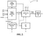
- FIG. 2further illustrates an example carrier loop 30 , exemplary of an embodiment of the present invention.
- carrier loop 30includes a multi-mode carrier phase error detector 50 , a loop filter 52 , an adaptive gain circuit 54 , a low pass filter 56 to filter the output of adaptive gain circuit 54 , a sine/cosine generator 58 , and a mode control block 60 .
- Mode control block 60assumes a number of states based on the state of receiver 10 (e.g. initial signal acquisition mode, tracking mode, etc.) and the quality of the received signal, and generates control signals to select the appropriate phase error detector 50 , and to loop filter 52 controlling one of multiple modes of operation of each of detector 50 and loop filter 52 , as detailed below.
- Example carrier phase error detector 50computes the phase error in the carrier from three inputs: input to slicer 38 (y(n)— FIG. 1 ), carrier corrected output of FFE 26 (real component of the complex valued derot(n)); and output of slicer 38 (S(n)). Using these inputs, detector 50 estimates the error that is caused by offset between carrier frequency and phase at the receiver and transmitter. Phase error in the carrier may be estimated in a number of ways. For example, phase error may be estimated by calculating the phase difference between the demodulated signal at the input and output of slicer 38 .
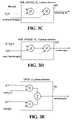
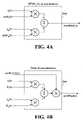
- Example carrier phase error detector 50includes seven phase error detector calculation blocks illustrated in FIGS. 3A-3E , FIGS. 4A-4B to calculate metrics to estimate the error in the imaginary (errorImag(n)) and real part (errorReal(n)) of the demodulated signal. These blocks are labelled DD_CL (block 62 a — FIG. 3A ), DD_CL_ALT (block 62 b — FIG. 3B ), MSE_SINGLE_CL_I (block 62 a — FIG. 3C ), MSE_SINGLE_CL_Q (block 62 d — FIG. 3D ), QPSK_CL (block 62 e — FIGS. 3E and 64 a — FIG. 4A ) and other (block 64 b — FIG. 4B ).
- DD_CLblock 62 a — FIG. 3A
- DD_CL_ALTblock 62 b — FIG. 3B
- MSE_SINGLE_CL_Iblock 62
- errorReal(n)may be determined as
- errorNormImag(n), and errorRealnorm(n)may be derived from the magnitudes of S i (n) and S q (n). These normalization factors normalize the amplitude of the different metrics and thus the phase error estimation resulting form the metrics.
- the normalization factorsare formed from S i (n) and S q (n) typically using a look-up table by block 100 a , of phase error detector 50 illustrated in FIG. 5B .
- errorNormImag1/2 ⁇ *(
- a minimal normalization valueis applied when both components are close to zeros.
- qpsk i (n) and qpsk q (n)are quadrature phase keyed approximations of y i (n) and y q (n), respectively. These are formed from y i (n) and y q (n) using a look-up table by block 100 b , of phase error detector 50 illustrated in FIG. 5B .
- block 100 bforms qpsk i (n) and qpsk q (n) as follows:
- S(n) and y(n)are real. The following may be used to assess phase error using blocks 62 a - 62 e and 64 a and 64 b and 100 a and 100 b .
- the input S i (n) and S q (n) and the output y i (n) and y q (n)are interpreted as follow:
- the inputs for the exemplary QPSK phase detectorare:
- Phase error detector 50thus generates two error signals; errorImag(n) and errorReal(n) using one of blocks 62 a - 62 e for errorImag(n), and block 64 a for errorReal(n) when 62 e is used for errorImag(n) and block 64 b for errorReal(n), for all other phase detector functions are used.
- the errorImag(n) phase detectors 62 a , 62 e and the errorReal(n) error signals 64 a and 64 bare the only signals used to compute the phase/frequency estimation.
- mode control block 60provides a signal to select one of three modes to phase error detector 50 reflective of whether the quality of the received signal demonstrates high reliability; low reliability; or intermediate reliability.
- the quality of the received signalmay be assessed in any number of ways by mode control block 60 , including measuring errors in reference/training portions of the received signal, measuring the signal to noise ratio, measuring the evolutions of the equalizer coefficient over time, measuring estimates of the signal spectrum over time, measuring variations of the signal in time, etc. or any suitable combinations of such measurements.
- Mode control block 60may accordingly additionally be provided with signals allowing such measurements.
- the results of block 62 a or 62 bmay be used when the signal is reliable and the receiver 10 is tracking the demodulated signal.
- the reliability of the signalmay be estimated by monitoring the variance of symbols y(n) over time in conjunction with a measure of variance over time of one or multiple coefficients of the DFE 36 and FFE 26 .
- the results of block 62 e ( FIG. 3E ) and block 64 amay be used for a low reliability signal, exhibited by high variance coefficients.
- phase detectorswill be used during a cold start initialisation of the receiver.
- the output of blocks 62 e and 64 amay, for example be used for ATSC signals after frames are detected.
- the results of block 62 c or 62 d( FIGS. 3C , 3 D—MSE_SINGLE_CL_I, MSE_SINGLE CL_Q) and block 64 b (FIG. 4 B—Other) may be used between these extreme signal conditions, such as for example, in the presence of an atypical event, which may lead to the loss of signal equalization.
- Atypical eventsinclude burst noise detection, abrupt change is signal gain, high jitter in the output of blocks 62 a or 62 b or abrupt changes in the adaptation of the coefficients of the FFE 26 or DFE 36 .
- phase correction angle estimate ⁇ (n)is filtered by loop filter 52 to provide a phase correction angle estimate ⁇ (n).
- Sine/cosine signal generator 58converts phase correction angle ⁇ (n) to generate a signal which is mixed by multiplier 28 with the output of FFE 26 ( FIG. 1 ) to de-rotate the output of FFE 26 to correct for carrier phase and frequency offsets.
- sine/cosine generator 58provides two output values corresponding to the sine and cosine of ⁇ (n) derived from the phase error estimate errorImag(n), calculated by phase error detector 50 and loop filter 52 .
- Sine/cosine valuesmay be calculated by a suitable look-up table.
- Mixer 28FIG. 1 ) multiplies the complex signal derot(n) by the complex quantity cos ⁇ (n)+j sin ⁇ (n) (i.e. e j ⁇ (n) ).
- loop filter 52takes as adaptive gain inputs, the output of an adaptive gain circuit 54 and an associated low pass filter 56 .
- Adaptive gain circuit 54takes errorImag(n) and errorReal(n) and adapts the gain of loop filter 52 to optimize the performance of carrier recovery circuit 29 .
- FIG. 6illustrates loop filter 52 of carrier loop 30 .
- Example filter 52is formed as second order phase locked loop (PLL) in order to track both the phase and frequency offset in the carrier.
- Loop filter 52may be operated in one of three modes: a non-adaptive mode of operation and two adaptive modes. Again, the mode of operation of loop filter 52 is controlled by mode control block 60 , in dependence on the operating state of receiver 10 , and the quality of the received signal.
- the non-adaptive modemay be used during receiver initialization; the first adaptive mode may be used during signal tracking (high quality signal reception); the second adaptive mode may be used for low and intermediate quality signals.
- the mode of operation for the phase error detector 50is selected in tandem with a specific phase error detector.
- the phase error detector of block 62 eQPSK_CL phase detector
- the phase error detector of block 62 a or block 62 bDD_CL; DD_CL_ALT phase detectors
- all adaptive gainsare computed in parallel, but are used by filter 52 only when needed. This mode of operation allows seamless transitions between fixed and variable gains.
- gain of loop filter 52is programmable through three programmable registers k 0 , k 1 , k 2 .
- Suitable values of k 0 , k 1 and k 2 for the non-adaptive mode of operationmay be hard coded, or provided by a controller (not shown) controlling overall operation of receiver 10 .
- a multiplier 70multiplies errorImag(n) by a scale factor k 1 .
- errorImag(n)is similarly multiplied by k 2 at multiplier 68 .
- Delayed versions of multiplied signalsare fed-back through delay blocks 78 and 80 , and added by adders 74 and 76 .
- a further delayed scaled version of the delayed multiplied signal, delayed by delay block 77 and scaled by the value of k 0 by multiplier 79is fed back to adder 74 .
- ⁇ ( n )⁇ ( n ⁇ 1)+ k 2 errorImag( n ⁇ 1)
- ⁇ ( n )(1 ⁇ k 0 ) ⁇ ( n ⁇ 1)+ k 1 ⁇ errorImag( n ⁇ 1)+ ⁇ ( n )
- errorImag(n)is the output of phase error detector 50 for symbol S(n).
- ⁇ (n)is now the frequency offset estimate, and ⁇ (n) is phase offset estimate.
- filter 52in its non-adaptive mode, is second order.
- k 0increases the range of phase errors to which loop filter 52 can lock.
- k 0induces a low pass filtering of the phase estimation which contributes to reduce impulsive phase noise that may be triggered in the VSB receiver by abrupt changes in the equalizer coefficients.
- Loop filter 52may be used in its non-adaptive mode at start-up (as controlled by mode control block 60 ). In the event the errorImag(n) exceeds a threshold, as may for example be caused by noise, errorImag(n) is clipped at block 66 . In the event the errorImag(n) does exceed the threshold, a value of zero (0) is provided by block 64 , ensuring stability of loop 30 .
- filters 52could be made adaptive in many other ways.
- exemplary filter 52is first order in its adaptive mode.
- the phase offset ⁇ (n)is calculated with a first order loop filter for which the gain is adaptive (i.e. the gain is a function of the past observation).
- the adaptive gainallows the carrier loop to adapt to abrupt variations of phase/frequency.
- exemplary loop filter 52calculates over time ⁇ (n) that minimizes an error comparable to the error detected by phase detector 50 , operating in its selected mode using gradient stochastic optimisation.
- the gradient stochastic optimizationuses variable gain k 1 adapt computed by block 54 .
- Variable gain k 1 adaptis calculated and adjusted adaptively as described below to track the variation of the channel over time which allows atrade-off between a fast change in the channel and an accurate estimate of the phase.
- an optimal gain k 1 adaptis calculated to optimize a cost function. For example, in the case of the single-axis constant modulus, cost
- k 1another gradient optimisation with respect k 1 is used.
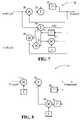
- FIG. 7schematically illustrates the adaptive gain controller 54 of carrier loop 30 .
- Adaptive gain controller 54calculates k 1 adapt(n) from past values of the phase error as estimated by phase error detector 50 .
- Low pass filter 56additionally calculates k 1 adaptavg(n), a filtered, averaged version of k 1 adapt(n).
- the structure of an example low pass filter 56is illustrated schematically in FIG. 8 .
- k 1 adaptavg(n)may be used in the second adaptive mode of filter 52 instead of k 1 adapt(n).
- ⁇controls the bandwidth of filter 52 .
- ⁇is selected close to 1. Suitable values of ⁇ and ⁇ may be hard coded, or provided by a controller (not shown) controlling overall operation of receiver 10 .
- a first order loop 52 with a low pass filterallows loop gain, k 1 adapt, to be computed by block 54 as a function of phase detector error to minimize error in the decoded symbol y(n) in much the same way as the phase offset estimate ⁇ (n) is calculated to minimize error in the decoded symbol y(n) by block 52 .
- Thisallows adjustment of the bandwidth of loop filter 52 continuously over time.
- loop gain k 1 adaptis adaptive changing on a symbol by symbol basis
- loop 52provides performance of a second order loop which allows tracking of frequency variation, using only a first order loop.
- this approachtakes into account any hidden parametric model affecting the variations of the RF signal frequency.
- receiver 10using adaptive loop filter 52 may better track time varying channels such as an RF channel for a moving receiver.
- the example receivermay better track a signal whose frequency is changing over time due to a Doppler shift. This may occur when a vehicle, such as a car or an airplane, is moving in the vicinity of a stationary receiver. Without adapting loop filter 52 , it is difficult to first detect a Doppler shift and then compute optimum gains k 1 , k 2 as these change continuously. If not processed adequately the phase correction would generally lead to a corruption of the symbol y(n) which will lead ultimately to a failure of the equalizer in the tracking mode.
- FIG. 9illustrates a QAM receiver 10 ′, similar to VSB receiver 10 and exemplary of an embodiment of the present invention.
- QAMquadrature amplitude modulation
- two orthogonal data streamsare transmitted at the same time.
- each symbol's I valuetakes one of eight relative values: ⁇ 7, ⁇ 5, ⁇ 3, ⁇ 1, 1, 3, 5, and 7, so does the Q value.
- For QAM256each symbol's I value takes one of sixteen values: ⁇ 15, ⁇ 13, ⁇ 11, ⁇ 9, ⁇ 7, ⁇ 5, ⁇ 3, ⁇ , 1, 3, 5, 7, 9, 11, and 15 so does the Q value.
- Receiver 10 ′is similar to receiver 10 sharing many identical components. As such, like components have been marked with like numerals and will not be further detailed herein. Components similar to those of receiver 10 , but adapted to operate on a QAM stream have been but including a prime (′) symbol. Adaptation of these components to process QAM signals will be apparent to those of ordination skill.
- slicer 38 ′may produce complex signals S(n) in the QAM constellation from complex signals y(n).
- FFE 26 ′ and DFE 36 ′are formed with complex filter parameter suitable for QAM signals. Interconnection between components reflects complex quantities, including real and imaginary data, transferred between functional blocks.
- phase errormay be derived by loop filter 52 from S(n) and y(n). Indeed, use of derot(n) to produce a phase error estimate of the carrier is no longer required.
- phase errorsmay be calculated by the equivalents of blocks 62 a - 62 e and 64 a - 64 b and 100 a - 100 b using complex valued S(n), y(n) and qpsk (i.e. actual S i (n), S q (n), y i (n), y q (n) qpsk i (n), qpsk q (n)) using these blocks.
- Loop filter, adaptive gain circuit, and low pass filter of carrier loop 30 ′may otherwise be formed in manners identical to loop filter 52 , adaptive gain control 54 and low pass filter 56 of receiver 10 .
- carrier recovery circuit 29 ′(and particularly mixer 28 ′) is downstream of summer 34 (unlike in receiver 10 ).
- a further mixer 31 ′re-rotates the output of slicer 38 ′ by an angle of ⁇ (n) so as not to lose information in the signal output by slicer 38 ′, indicative of a phase error in the received signal.
- receiver 10 and receiver 10 ′use common and similar components, these receivers could be combined to form a multi-mode receiver capable of receiving VSB or QAM signal.
- VSB/QAM modecould be toggled externally.
Landscapes
- Engineering & Computer Science (AREA)
- Computer Networks & Wireless Communication (AREA)
- Signal Processing (AREA)
- Power Engineering (AREA)
- Digital Transmission Methods That Use Modulated Carrier Waves (AREA)
Abstract
Description
- (yi(n)*Sq(n)−yq(n)Si(n))*errorNormImag (block62a,
FIG. 3A ); - sign(derotq(n))*(yi(n)−Si(n))*errorNormImag (block62b,
FIG. 3B );
where sign(derotq(n)) extracts the sign of derot(n) - deroti(n)*Sq(n)*errorNormImag (block62c,
FIG. 3C ); - −derotq(n)*Si(n)*errorNormImag (block62d,
FIG. 3D ); or - yi(n)*qpskq(n)−yq(n)*qpksi(n) (block62e,
FIG. 3E );
- (yi(n)*Sq(n)−yq(n)Si(n))*errorNormImag (block62a,
- (yi(n)*qpski(n)+yq(n)*qpskq(n)) (block64a,
FIG. 4A ); or - (Si(n)*yi(n)+Sq(n)*yq(n))*errorNormImag, (block64b,
FIG. 4B );
- (yi(n)*qpski(n)+yq(n)*qpskq(n)) (block64a,
- errorNormImag may be calculated by
block 100aas, - errorNormImag=1/(2π*(|Si(n)|+|Sq(n)|)), where |Si(n)| and |Sq(n)| denote respectively the magnitude of Si(n) and Sq(n).
- errorNormImag may be calculated by
- qpski(n)=1/(16*π) if yi(n)>0 and
- qpski(n)=−1/(16*π) if yi(n)<0,
- qpskq(n)=1/(16*π) if yq(n)>0 and
- qpskq(n)=−1/(16*π) if yq(n)<0
- Si(n)=S(n), Sq(n)=S(n−1)
- yi(n)=y(n), yq(n)=y(n−1)
- qpski(n)=qpsk(n), qpskq(n)=qpsk(n−1)
θ(n)=θ(n−1)+k2errorImag(n−1)
φ(n)=(1−k0)×φ(n−1)+
where errorImag(n) is the output of
θ(n)=θ(n−1)
φ(n)=(1−k0)×φ(n−1)+k1adapt×errorImag(n−1)+θ(n)
[or φ(n)=(1−k0)×φ(n−1)+k1adaptavg×errorImag(n−1)+θ(n)]
Of course filters52 could be made adaptive in many other ways. In this mode, the frequency offset θ(n) is assumed to be correct and a constant over time. Unlike in its non-adaptive mode,
is optimised with respect θ(n) and the gain k1 under the constraint that the gradient estimate of θ(n) can be expressed in the form θ(n)=θ(n−1)+k1Δ, where Δ is the derivative of the constant modulus cost function with respect to θ. To estimate k1adapt, another gradient optimisation with respect k1 is used.
k1adapt(n)=k1adapt(n−1)+2γα(n−1)errorImag(n−1))
α(n)=(1−k1adapt(n−1)*errorReal(n)*α(n−1)−errorImag(n))
where γ is a small positive auxiliary step size.
k1adaptavg(n)=λ*k1adapt(n)+(1−λ)*k1adaptavg(n−1)
k1adaptavg(n) may be used in the second adaptive mode of
Claims (44)
k1adapt(n)=k1adapt(n−1)+2γα(n−1)errorImag(n−1)), where
α(n)=(1−k1adapt(n−1)*errorReal(n)*α(n−1) errorImag(n))
φ(n)=(1−k0)xφ(n−1)+k1adapt ×errorImag(n−1)+0
k1adapt(n)=k1adapt(n−1)+2γα(n−1)errorImag(n−1)), where
α(n)=(1−k1adapt(n−1)*errorReal(n)*α(n−1)−errorImag(n))
k1adapt(n)=k1adapt(n−1)+2γα(n−1)errorImag(n−1 )), where
α(n)=(1−k1adapt(n−1)*errorReal(n)*α(n−1) errorImag(n))
φ(n)=(1−k0)xφ(n−1)+k1adapt ×errorImag(n−1)+θ
Priority Applications (1)
| Application Number | Priority Date | Filing Date | Title |
|---|---|---|---|
| US10/757,536US7342981B2 (en) | 2004-01-15 | 2004-01-15 | Digital receiver having adaptive carrier recovery circuit |
Applications Claiming Priority (1)
| Application Number | Priority Date | Filing Date | Title |
|---|---|---|---|
| US10/757,536US7342981B2 (en) | 2004-01-15 | 2004-01-15 | Digital receiver having adaptive carrier recovery circuit |
Publications (2)
| Publication Number | Publication Date |
|---|---|
| US20050157820A1 US20050157820A1 (en) | 2005-07-21 |
| US7342981B2true US7342981B2 (en) | 2008-03-11 |
Family
ID=34749396
Family Applications (1)
| Application Number | Title | Priority Date | Filing Date |
|---|---|---|---|
| US10/757,536Expired - Fee RelatedUS7342981B2 (en) | 2004-01-15 | 2004-01-15 | Digital receiver having adaptive carrier recovery circuit |
Country Status (1)
| Country | Link |
|---|---|
| US (1) | US7342981B2 (en) |
Cited By (13)
| Publication number | Priority date | Publication date | Assignee | Title |
|---|---|---|---|---|
| US20040157626A1 (en)* | 2003-02-10 | 2004-08-12 | Vincent Park | Paging methods and apparatus |
| US20060045209A1 (en)* | 2004-08-27 | 2006-03-02 | Dong-Hoon Lee | Carrier recovery apparatus usable with VSB type receiver and method thereof |
| US20060098728A1 (en)* | 2003-02-11 | 2006-05-11 | Sung-Ik Park | Decision feedback equalizer for digital tv and method thereof |
| US20060251195A1 (en)* | 2005-05-05 | 2006-11-09 | Chung-Jue Chen | State based algorithm to minimize mean squared error |
| US20070033476A1 (en)* | 2005-07-21 | 2007-02-08 | Stmicroelectronics S.R.L. | Method and system for decoding signals, corresponding receiver and computer program product |
| US20070234175A1 (en)* | 2003-04-02 | 2007-10-04 | Qualcomm Incorporated | Methods and apparatus for interleaving in a block-coherent communication system |
| US20080107168A1 (en)* | 2004-04-09 | 2008-05-08 | Micronas Semiconductors, Inc. | Advanced Digital Receiver |
| US20080123787A1 (en)* | 2006-11-29 | 2008-05-29 | Supat Wongwirawat | Method and apparatus for detecting and correcting modulated signal impairments |
| US20110069789A1 (en)* | 2009-09-21 | 2011-03-24 | Honghui Xu | Method and system for carrier recovery for qam |
| US8483317B2 (en) | 2004-04-09 | 2013-07-09 | Entropic Communications, Inc. | Apparatus for and method of controlling sampling frequency and sampling phase of a sampling device |
| US9276782B1 (en)* | 2015-04-28 | 2016-03-01 | Xilinx, Inc. | Precursor inter-symbol interference reduction |
| US11595137B1 (en)* | 2021-02-17 | 2023-02-28 | Keysight Technologies, Inc. | System and method of measuring error vector magnitude in the time domain |
| US20240259038A1 (en)* | 2021-07-29 | 2024-08-01 | St Engineering Idirect (Europe) Cy Nv | Method for estimating phase noise |
Families Citing this family (80)
| Publication number | Priority date | Publication date | Assignee | Title |
|---|---|---|---|---|
| US7434145B2 (en)* | 2003-04-02 | 2008-10-07 | Qualcomm Incorporated | Extracting soft information in a block-coherent communication system |
| US7477325B2 (en)* | 2004-03-29 | 2009-01-13 | Ati Technologies, Inc. | Audio/video separator |
| TWI258085B (en)* | 2005-04-12 | 2006-07-11 | Univ Nat Taiwan | Soft-threshold-based multi-layer decision feedback equalizer and decision method |
| US7706474B2 (en)* | 2005-11-14 | 2010-04-27 | Ibiquity Digital Corporation | Carrier tracking for AM in-band on-channel radio receivers |
| US7590174B2 (en)* | 2005-12-20 | 2009-09-15 | Altera Corporation | Signal adjustment receiver circuitry |
| US8537883B1 (en) | 2007-02-02 | 2013-09-17 | Marvell International Ltd. | Detector for low frequency offset distortion |
| US8111739B1 (en)* | 2007-02-02 | 2012-02-07 | Marvell International Ltd. | Detector for low frequency offset distortion |
| US7796688B2 (en)* | 2007-05-22 | 2010-09-14 | Freescale Semiconductor, Inc. | Radio receiver having a channel equalizer and method therefor |
| US8212941B2 (en)* | 2008-04-30 | 2012-07-03 | Mediatek Inc. | Digitized analog TV signal processing system |
| US11943089B2 (en) | 2010-05-28 | 2024-03-26 | Cohere Technologies, Inc. | Modulation and equalization in an orthonormal time-shifting communications system |
| US8976851B2 (en) | 2011-05-26 | 2015-03-10 | Cohere Technologies, Inc. | Modulation and equalization in an orthonormal time-frequency shifting communications system |
| US9071285B2 (en) | 2011-05-26 | 2015-06-30 | Cohere Technologies, Inc. | Modulation and equalization in an orthonormal time-frequency shifting communications system |
| US9130638B2 (en)* | 2011-05-26 | 2015-09-08 | Cohere Technologies, Inc. | Modulation and equalization in an orthonormal time-frequency shifting communications system |
| US10667148B1 (en) | 2010-05-28 | 2020-05-26 | Cohere Technologies, Inc. | Methods of operating and implementing wireless communications systems |
| US9444514B2 (en) | 2010-05-28 | 2016-09-13 | Cohere Technologies, Inc. | OTFS methods of data channel characterization and uses thereof |
| US9071286B2 (en) | 2011-05-26 | 2015-06-30 | Cohere Technologies, Inc. | Modulation and equalization in an orthonormal time-frequency shifting communications system |
| US10681568B1 (en) | 2010-05-28 | 2020-06-09 | Cohere Technologies, Inc. | Methods of data channel characterization and uses thereof |
| CA2814203C (en)* | 2010-10-29 | 2017-07-04 | Lilee Systems, Ltd | System and method of frequency offset compensation for radio system with fast doppler shift |
| US9083471B2 (en)* | 2011-03-03 | 2015-07-14 | Technion Research And Development Foundation Ltd. | Coherent and self-coherent signal processing techniques |
| EP2754249A4 (en)* | 2011-09-09 | 2015-07-01 | Entropic Communications Inc | Systems and methods for performing phase tracking within an adc-based tuner |
| WO2013130042A1 (en)* | 2012-02-28 | 2013-09-06 | Intel Corporation | Dynamic optimization of carrier recovery performance for communications systems |
| US10003487B2 (en) | 2013-03-15 | 2018-06-19 | Cohere Technologies, Inc. | Symplectic orthogonal time frequency space modulation system |
| US10469215B2 (en) | 2012-06-25 | 2019-11-05 | Cohere Technologies, Inc. | Orthogonal time frequency space modulation system for the Internet of Things |
| US10411843B2 (en) | 2012-06-25 | 2019-09-10 | Cohere Technologies, Inc. | Orthogonal time frequency space communication system compatible with OFDM |
| US9929783B2 (en) | 2012-06-25 | 2018-03-27 | Cohere Technologies, Inc. | Orthogonal time frequency space modulation system |
| US9912507B2 (en) | 2012-06-25 | 2018-03-06 | Cohere Technologies, Inc. | Orthogonal time frequency space communication system compatible with OFDM |
| US10090972B2 (en) | 2012-06-25 | 2018-10-02 | Cohere Technologies, Inc. | System and method for two-dimensional equalization in an orthogonal time frequency space communication system |
| US9042490B2 (en)* | 2012-08-30 | 2015-05-26 | The Boeing Company | Systems and methods for carrier phase recovery |
| US9246587B2 (en)* | 2013-04-15 | 2016-01-26 | Broadcom Corporation | Compensation for optical multi-path interference |
| US20140347564A1 (en)* | 2013-05-27 | 2014-11-27 | Lin Yang | Wi-Fi ATSC TV Antenna With Waveform Compression |
| US20150052574A1 (en)* | 2013-08-16 | 2015-02-19 | M&A Holdings | Software defined atsc tv demodulator with wi-fi tuners |
| US10090973B2 (en) | 2015-05-11 | 2018-10-02 | Cohere Technologies, Inc. | Multiple access in an orthogonal time frequency space communication system |
| EP3295572A4 (en) | 2015-05-11 | 2018-12-26 | Cohere Technologies, Inc. | Systems and methods for symplectic orthogonal time frequency shifting modulation and transmission of data |
| US10574317B2 (en) | 2015-06-18 | 2020-02-25 | Cohere Technologies, Inc. | System and method for providing wireless communication services using configurable broadband infrastructure shared among multiple network operators |
| US9866363B2 (en) | 2015-06-18 | 2018-01-09 | Cohere Technologies, Inc. | System and method for coordinated management of network access points |
| CN112532558B (en) | 2015-06-27 | 2024-12-10 | 凝聚技术股份有限公司 | Orthogonal time-frequency space communication system compatible with OFDM |
| US10693581B2 (en) | 2015-07-12 | 2020-06-23 | Cohere Technologies, Inc. | Orthogonal time frequency space modulation over a plurality of narrow band subcarriers |
| US9455847B1 (en)* | 2015-07-27 | 2016-09-27 | Sanguoon Chung | Wireless communication apparatus with phase noise mitigation |
| EP3348015B1 (en) | 2015-09-07 | 2022-09-07 | Cohere Technologies, Inc. | Multiple access using orthogonal time frequency space modulation |
| WO2017087706A1 (en) | 2015-11-18 | 2017-05-26 | Cohere Technologies | Orthogonal time frequency space modulation techniques |
| CN108781072B (en) | 2015-12-09 | 2022-04-26 | 凝聚技术公司 | Pilot encapsulation using complex orthogonal functions |
| US10666314B2 (en) | 2016-02-25 | 2020-05-26 | Cohere Technologies, Inc. | Reference signal packing for wireless communications |
| EP3433969B1 (en) | 2016-03-23 | 2021-11-03 | Cohere Technologies, Inc. | Receiver-side processing of orthogonal time frequency space modulated signals |
| US9667307B1 (en) | 2016-03-31 | 2017-05-30 | Cohere Technologies | Wireless telecommunications system for high-mobility applications |
| WO2017173160A1 (en) | 2016-03-31 | 2017-10-05 | Cohere Technologies | Channel acquisition using orthogonal time frequency space modulated pilot signal |
| EP3437197B1 (en) | 2016-04-01 | 2022-03-09 | Cohere Technologies, Inc. | Tomlinson-harashima precoding in an otfs communication system |
| WO2017173389A1 (en) | 2016-04-01 | 2017-10-05 | Cohere Technologies | Iterative two dimensional equalization of orthogonal time frequency space modulated signals |
| WO2017201467A1 (en) | 2016-05-20 | 2017-11-23 | Cohere Technologies | Iterative channel estimation and equalization with superimposed reference signals |
| EP3497785B1 (en) | 2016-08-12 | 2024-03-13 | Cohere Technologies, Inc. | Method for multi-user multiplexing of orthogonal time frequency space signals |
| EP3497799A4 (en) | 2016-08-12 | 2020-04-15 | Cohere Technologies, Inc. | ITERATIVE MULTI-STAGE EQUALIZATION AND DECODING |
| EP3497907A4 (en) | 2016-08-12 | 2020-03-04 | Cohere Technologies, Inc. | LOCALIZED EQUALIZATION FOR CHANNELS WITH INTERMEDIATE INTERFERENCE INTERFERENCES |
| US11310000B2 (en) | 2016-09-29 | 2022-04-19 | Cohere Technologies, Inc. | Transport block segmentation for multi-level codes |
| EP3520310B1 (en) | 2016-09-30 | 2021-10-27 | Cohere Technologies, Inc. | Uplink user resource allocation for orthogonal time frequency space modulation |
| EP3549200B1 (en) | 2016-12-05 | 2022-06-29 | Cohere Technologies, Inc. | Fixed wireless access using orthogonal time frequency space modulation |
| US10355889B1 (en)* | 2016-12-12 | 2019-07-16 | Cadence Design Systems, Inc. | Adaptive pattern filtering for clock and data recovery to minimize interaction with decision feedback equalization |
| EP3566379B1 (en) | 2017-01-09 | 2024-12-11 | Cohere Technologies, Inc. | Pilot scrambling for channel estimation |
| US10356632B2 (en) | 2017-01-27 | 2019-07-16 | Cohere Technologies, Inc. | Variable beamwidth multiband antenna |
| US10568143B2 (en) | 2017-03-28 | 2020-02-18 | Cohere Technologies, Inc. | Windowed sequence for random access method and apparatus |
| EP3610582A4 (en) | 2017-04-11 | 2021-01-06 | Cohere Technologies, Inc. | Digital communication using dispersed orthogonal time frequency space modulated signals |
| EP4109983A1 (en) | 2017-04-21 | 2022-12-28 | Cohere Technologies, Inc. | Communication techniques using quasi-static properties of wireless channels |
| EP3616265A4 (en) | 2017-04-24 | 2021-01-13 | Cohere Technologies, Inc. | Multibeam antenna designs and operation |
| WO2018200577A1 (en) | 2017-04-24 | 2018-11-01 | Cohere Technologies | Digital communication using lattice division multiplexing |
| US9954712B1 (en)* | 2017-06-23 | 2018-04-24 | Intel Corporation | Blind decoding in orthogonal frequency division multiplexing (OFDM) communication systems |
| EP3652907A4 (en) | 2017-07-12 | 2021-04-07 | Cohere Technologies, Inc. | DATA MODULATION SCHEMES BASED ON ZAK TRANSFORMATION |
| US11546068B2 (en) | 2017-08-11 | 2023-01-03 | Cohere Technologies, Inc. | Ray tracing technique for wireless channel measurements |
| WO2019036492A1 (en) | 2017-08-14 | 2019-02-21 | Cohere Technologies | Transmission resource allocation by splitting physical resource blocks |
| EP3679493B1 (en) | 2017-09-06 | 2024-03-13 | Cohere Technologies, Inc. | Lattice reduction in orthogonal time frequency space modulation |
| US11283561B2 (en) | 2017-09-11 | 2022-03-22 | Cohere Technologies, Inc. | Wireless local area networks using orthogonal time frequency space modulation |
| US11190308B2 (en) | 2017-09-15 | 2021-11-30 | Cohere Technologies, Inc. | Achieving synchronization in an orthogonal time frequency space signal receiver |
| US11532891B2 (en) | 2017-09-20 | 2022-12-20 | Cohere Technologies, Inc. | Low cost electromagnetic feed network |
| WO2019068053A1 (en) | 2017-09-29 | 2019-04-04 | Cohere Technologies, Inc. | Forward error correction using non-binary low density parity check codes |
| EP4362344A3 (en) | 2017-11-01 | 2024-07-31 | Cohere Technologies, Inc. | Precoding in wireless systems using orthogonal time frequency space multiplexing |
| WO2019113046A1 (en) | 2017-12-04 | 2019-06-13 | Cohere Technologies, Inc. | Implementation of orthogonal time frequency space modulation for wireless communications |
| US10505768B2 (en)* | 2017-12-12 | 2019-12-10 | Huawei Technologies Co., Ltd. | Partially disjoint equalization and carrier recovery |
| FR3076412A1 (en)* | 2017-12-29 | 2019-07-05 | Avantix | System for the blind demodulation of digital telecommunication signals |
| WO2019157230A1 (en) | 2018-02-08 | 2019-08-15 | Cohere Technologies, Inc. | Aspects of channel estimation for orthogonal time frequency space modulation for wireless communications |
| US11489559B2 (en) | 2018-03-08 | 2022-11-01 | Cohere Technologies, Inc. | Scheduling multi-user MIMO transmissions in fixed wireless access systems |
| WO2019241589A1 (en) | 2018-06-13 | 2019-12-19 | Cohere Technologies, Inc. | Reciprocal calibration for channel estimation based on second-order statistics |
| US11522600B1 (en) | 2018-08-01 | 2022-12-06 | Cohere Technologies, Inc. | Airborne RF-head system |
| EP4331193A4 (en) | 2021-04-29 | 2024-10-30 | Cohere Technologies, Inc. | ULTRA WIDEBAND SIGNALS WITH ORTHOGONAL TIME-FREQUENCY SPACE MODULATION |
Citations (12)
| Publication number | Priority date | Publication date | Assignee | Title |
|---|---|---|---|---|
| US4691176A (en) | 1986-03-17 | 1987-09-01 | General Electric Company | Adaptive carrier tracking circuit |
| US5604648A (en)* | 1992-06-26 | 1997-02-18 | Goldstar Co., Ltd. | Circuit and method for controlling speed and phase of VCR servo system |
| US5703597A (en) | 1995-12-22 | 1997-12-30 | Alliedsignal, Inc. | Adaptive carrier phase lock loop in a GPS receiver |
| US5712873A (en)* | 1996-06-04 | 1998-01-27 | Thomson Consumer Electronics, Inc. | Multi-mode equalizer in a digital video signal processing system |
| US6018556A (en) | 1996-11-21 | 2000-01-25 | Dsp Group, Inc. | Programmable loop filter for carrier recovery in a radio receiver |
| US20020080516A1 (en)* | 2000-11-24 | 2002-06-27 | Bhakta Bhavesh G. | Implementation method of digital phase-locked loop |
| US6418164B1 (en)* | 1999-01-14 | 2002-07-09 | Nxtwave Communications, Inc. | Adaptive equalizer with enhanced error quantization |
| US6668014B1 (en)* | 1999-12-09 | 2003-12-23 | Ati Technologies Inc. | Equalizer method and apparatus using constant modulus algorithm blind equalization and partial decoding |
| US6671339B1 (en)* | 1999-07-13 | 2003-12-30 | Lg Electronics Inc. | Lock detecting apparatus and method for multimedia digital broadcasting receiver |
| US6696886B1 (en)* | 2002-11-18 | 2004-02-24 | Industrial Technology Research Institute | Automatically adjusting gain/bandwidth loop filter |
| US6868129B2 (en)* | 2001-03-12 | 2005-03-15 | Freescale Semiconductor, Inc. | Demodulator for a radio receiver and method of operation |
| US7027500B1 (en)* | 2000-12-12 | 2006-04-11 | Ati Research, Inc. | Linear prediction based initialization of a single-axis blind equalizer for VSB signals |
- 2004
- 2004-01-15USUS10/757,536patent/US7342981B2/ennot_activeExpired - Fee Related
Patent Citations (12)
| Publication number | Priority date | Publication date | Assignee | Title |
|---|---|---|---|---|
| US4691176A (en) | 1986-03-17 | 1987-09-01 | General Electric Company | Adaptive carrier tracking circuit |
| US5604648A (en)* | 1992-06-26 | 1997-02-18 | Goldstar Co., Ltd. | Circuit and method for controlling speed and phase of VCR servo system |
| US5703597A (en) | 1995-12-22 | 1997-12-30 | Alliedsignal, Inc. | Adaptive carrier phase lock loop in a GPS receiver |
| US5712873A (en)* | 1996-06-04 | 1998-01-27 | Thomson Consumer Electronics, Inc. | Multi-mode equalizer in a digital video signal processing system |
| US6018556A (en) | 1996-11-21 | 2000-01-25 | Dsp Group, Inc. | Programmable loop filter for carrier recovery in a radio receiver |
| US6418164B1 (en)* | 1999-01-14 | 2002-07-09 | Nxtwave Communications, Inc. | Adaptive equalizer with enhanced error quantization |
| US6671339B1 (en)* | 1999-07-13 | 2003-12-30 | Lg Electronics Inc. | Lock detecting apparatus and method for multimedia digital broadcasting receiver |
| US6668014B1 (en)* | 1999-12-09 | 2003-12-23 | Ati Technologies Inc. | Equalizer method and apparatus using constant modulus algorithm blind equalization and partial decoding |
| US20020080516A1 (en)* | 2000-11-24 | 2002-06-27 | Bhakta Bhavesh G. | Implementation method of digital phase-locked loop |
| US7027500B1 (en)* | 2000-12-12 | 2006-04-11 | Ati Research, Inc. | Linear prediction based initialization of a single-axis blind equalizer for VSB signals |
| US6868129B2 (en)* | 2001-03-12 | 2005-03-15 | Freescale Semiconductor, Inc. | Demodulator for a radio receiver and method of operation |
| US6696886B1 (en)* | 2002-11-18 | 2004-02-24 | Industrial Technology Research Institute | Automatically adjusting gain/bandwidth loop filter |
Non-Patent Citations (1)
| Title |
|---|
| Richard Citta & Gary Sgrignoli, "ATSC Transmission System: VSB Tutorial", Zenith Electronics Corporation, Montreuz Symposium, Jun. 12, 1997. |
Cited By (22)
| Publication number | Priority date | Publication date | Assignee | Title |
|---|---|---|---|---|
| US20070060175A1 (en)* | 2003-02-10 | 2007-03-15 | Vincent Park | Paging methods and apparatus |
| US20040157626A1 (en)* | 2003-02-10 | 2004-08-12 | Vincent Park | Paging methods and apparatus |
| US8233522B2 (en)* | 2003-02-11 | 2012-07-31 | Electronics And Telecommunications Research Institute | Decision feedback equalizer for digital TV and method thereof |
| US20060098728A1 (en)* | 2003-02-11 | 2006-05-11 | Sung-Ik Park | Decision feedback equalizer for digital tv and method thereof |
| US20070234175A1 (en)* | 2003-04-02 | 2007-10-04 | Qualcomm Incorporated | Methods and apparatus for interleaving in a block-coherent communication system |
| US8196000B2 (en) | 2003-04-02 | 2012-06-05 | Qualcomm Incorporated | Methods and apparatus for interleaving in a block-coherent communication system |
| US7995648B2 (en)* | 2004-04-09 | 2011-08-09 | Trident Microsystems (Far East) Ltd. | Advanced digital receiver |
| US8483317B2 (en) | 2004-04-09 | 2013-07-09 | Entropic Communications, Inc. | Apparatus for and method of controlling sampling frequency and sampling phase of a sampling device |
| US20080107168A1 (en)* | 2004-04-09 | 2008-05-08 | Micronas Semiconductors, Inc. | Advanced Digital Receiver |
| US8130873B2 (en)* | 2004-08-27 | 2012-03-06 | Samsung Electronics Co., Ltd. | Carrier recovery apparatus usable with VSB type receiver and method thereof |
| US20060045209A1 (en)* | 2004-08-27 | 2006-03-02 | Dong-Hoon Lee | Carrier recovery apparatus usable with VSB type receiver and method thereof |
| US7702053B2 (en)* | 2005-05-05 | 2010-04-20 | Broadcom Corporation | State based algorithm to minimize mean squared error |
| US20060251195A1 (en)* | 2005-05-05 | 2006-11-09 | Chung-Jue Chen | State based algorithm to minimize mean squared error |
| US8069399B2 (en)* | 2005-07-21 | 2011-11-29 | Stmicroelectronics, S.R.L. | Method and system for decoding signals, corresponding receiver and computer program product |
| US20070033476A1 (en)* | 2005-07-21 | 2007-02-08 | Stmicroelectronics S.R.L. | Method and system for decoding signals, corresponding receiver and computer program product |
| US20080123787A1 (en)* | 2006-11-29 | 2008-05-29 | Supat Wongwirawat | Method and apparatus for detecting and correcting modulated signal impairments |
| US20110069789A1 (en)* | 2009-09-21 | 2011-03-24 | Honghui Xu | Method and system for carrier recovery for qam |
| US8259859B2 (en)* | 2009-09-21 | 2012-09-04 | Techwell Llc | Method and system for carrier recovery for QAM |
| US9276782B1 (en)* | 2015-04-28 | 2016-03-01 | Xilinx, Inc. | Precursor inter-symbol interference reduction |
| US11595137B1 (en)* | 2021-02-17 | 2023-02-28 | Keysight Technologies, Inc. | System and method of measuring error vector magnitude in the time domain |
| US20240259038A1 (en)* | 2021-07-29 | 2024-08-01 | St Engineering Idirect (Europe) Cy Nv | Method for estimating phase noise |
| US12368460B2 (en)* | 2021-07-29 | 2025-07-22 | St Engineering Indirect (Europe) Cy Nv | Method for estimating phase noise |
Also Published As
| Publication number | Publication date |
|---|---|
| US20050157820A1 (en) | 2005-07-21 |
Similar Documents
| Publication | Publication Date | Title |
|---|---|---|
| US7342981B2 (en) | Digital receiver having adaptive carrier recovery circuit | |
| US7031405B1 (en) | Carrier phase estimation based on single-axis constant modulus cost criterion and Bussgang criteria | |
| US7027500B1 (en) | Linear prediction based initialization of a single-axis blind equalizer for VSB signals | |
| US6240133B1 (en) | High stability fast tracking adaptive equalizer for use with time varying communication channels | |
| US7580482B2 (en) | Joint, adaptive control of equalization, synchronization, and gain in a digital communications receiver | |
| US6668014B1 (en) | Equalizer method and apparatus using constant modulus algorithm blind equalization and partial decoding | |
| US7151797B2 (en) | Adaptive K-factor-improvement filter for receiver of radio signals subject to multipath distortion | |
| US6337878B1 (en) | Adaptive equalizer with decision directed constant modulus algorithm | |
| US20030219085A1 (en) | Self-initializing decision feedback equalizer with automatic gain control | |
| US7551679B2 (en) | Symmetrical data signal processing | |
| US8175193B2 (en) | Apparatus for recovering carrier wave in digital broadcasting receiver and method therefor | |
| JP4947603B2 (en) | Nonlinear signal distortion detection using multiple signal-to-noise ratio measurement sources | |
| US7006565B1 (en) | Hybrid soft and hard decision feedback equalizer | |
| US20050286625A1 (en) | Equalizer capable of adjusting step size and equalization method thereof | |
| KR100609941B1 (en) | Crystal-oriented phase detector | |
| KR100930988B1 (en) | Phase tracking system and method | |
| US9882709B2 (en) | Timing recovery with adaptive channel response estimation | |
| US8199864B1 (en) | Quadrature phase shift keying demodulator of digital broadcast reception system and demodulation method thereof | |
| US20050141660A1 (en) | Symbol timing recovery and broadcast receiver using the same | |
| US9503290B2 (en) | Diversity reception device, diversity reception method, reception program, and recording medium | |
| KR100510665B1 (en) | Apparatus and method for tracking phase error in digital TV receiver | |
| US7739320B2 (en) | Waveform equalizer, waveform equalization method, and integrated circuit | |
| US6445752B1 (en) | Apparatus and method for phase tracking in a demodulator | |
| KR100390433B1 (en) | Apparatus for tracking error of digital TV receiver | |
| KR100720562B1 (en) | Broadcast Signal Demodulation Apparatus and Method of Digital Broadcast Receiver |
Legal Events
| Date | Code | Title | Description |
|---|---|---|---|
| AS | Assignment | Owner name:ATI TECHNOLOGIES INC., CANADA Free format text:ASSIGNMENT OF ASSIGNORS INTEREST;ASSIGNORS:WONGWIRAWAT, SUPAT;TOUZNI, AZZEDINE;HRYSZKO, MARK;AND OTHERS;REEL/FRAME:014894/0682;SIGNING DATES FROM 20040112 TO 20040113 | |
| AS | Assignment | Owner name:ATI TECHNOLOGIES ULC, CANADA Free format text:CHANGE OF NAME;ASSIGNOR:ATI TECHNOLOGIES INC.;REEL/FRAME:021679/0230 Effective date:20061025 Owner name:ATI TECHNOLOGIES ULC,CANADA Free format text:CHANGE OF NAME;ASSIGNOR:ATI TECHNOLOGIES INC.;REEL/FRAME:021679/0230 Effective date:20061025 | |
| AS | Assignment | Owner name:BROADCOM CORPORATION, CALIFORNIA Free format text:ASSIGNMENT OF ASSIGNORS INTEREST;ASSIGNORS:ADVANCED MICRO DEVICES, INC.;ATI TECHNOLOGIES ULC;ATI INTERNATIONAL SRL;REEL/FRAME:022083/0433 Effective date:20081027 Owner name:BROADCOM CORPORATION,CALIFORNIA Free format text:ASSIGNMENT OF ASSIGNORS INTEREST;ASSIGNORS:ADVANCED MICRO DEVICES, INC.;ATI TECHNOLOGIES ULC;ATI INTERNATIONAL SRL;REEL/FRAME:022083/0433 Effective date:20081027 | |
| FPAY | Fee payment | Year of fee payment:4 | |
| REMI | Maintenance fee reminder mailed | ||
| AS | Assignment | Owner name:BANK OF AMERICA, N.A., AS COLLATERAL AGENT, NORTH CAROLINA Free format text:PATENT SECURITY AGREEMENT;ASSIGNOR:BROADCOM CORPORATION;REEL/FRAME:037806/0001 Effective date:20160201 Owner name:BANK OF AMERICA, N.A., AS COLLATERAL AGENT, NORTH Free format text:PATENT SECURITY AGREEMENT;ASSIGNOR:BROADCOM CORPORATION;REEL/FRAME:037806/0001 Effective date:20160201 | |
| LAPS | Lapse for failure to pay maintenance fees | ||
| STCH | Information on status: patent discontinuation | Free format text:PATENT EXPIRED DUE TO NONPAYMENT OF MAINTENANCE FEES UNDER 37 CFR 1.362 | |
| FP | Lapsed due to failure to pay maintenance fee | Effective date:20160311 | |
| AS | Assignment | Owner name:AVAGO TECHNOLOGIES GENERAL IP (SINGAPORE) PTE. LTD., SINGAPORE Free format text:ASSIGNMENT OF ASSIGNORS INTEREST;ASSIGNOR:BROADCOM CORPORATION;REEL/FRAME:041706/0001 Effective date:20170120 Owner name:AVAGO TECHNOLOGIES GENERAL IP (SINGAPORE) PTE. LTD Free format text:ASSIGNMENT OF ASSIGNORS INTEREST;ASSIGNOR:BROADCOM CORPORATION;REEL/FRAME:041706/0001 Effective date:20170120 | |
| AS | Assignment | Owner name:BROADCOM CORPORATION, CALIFORNIA Free format text:TERMINATION AND RELEASE OF SECURITY INTEREST IN PATENTS;ASSIGNOR:BANK OF AMERICA, N.A., AS COLLATERAL AGENT;REEL/FRAME:041712/0001 Effective date:20170119 | |
| AS | Assignment | Owner name:AVAGO TECHNOLOGIES INTERNATIONAL SALES PTE. LIMITE Free format text:MERGER;ASSIGNOR:AVAGO TECHNOLOGIES GENERAL IP (SINGAPORE) PTE. LTD.;REEL/FRAME:047195/0658 Effective date:20180509 | |
| AS | Assignment | Owner name:AVAGO TECHNOLOGIES INTERNATIONAL SALES PTE. LIMITE Free format text:CORRECTIVE ASSIGNMENT TO CORRECT THE EFFECTIVE DATE OF MERGER PREVIOUSLY RECORDED ON REEL 047195 FRAME 0658. ASSIGNOR(S) HEREBY CONFIRMS THE THE EFFECTIVE DATE IS 09/05/2018;ASSIGNOR:AVAGO TECHNOLOGIES GENERAL IP (SINGAPORE) PTE. LTD.;REEL/FRAME:047357/0302 Effective date:20180905 | |
| AS | Assignment | Owner name:AVAGO TECHNOLOGIES INTERNATIONAL SALES PTE. LIMITE Free format text:CORRECTIVE ASSIGNMENT TO CORRECT THE ERROR IN RECORDING THE MERGER PREVIOUSLY RECORDED AT REEL: 047357 FRAME: 0302. ASSIGNOR(S) HEREBY CONFIRMS THE ASSIGNMENT;ASSIGNOR:AVAGO TECHNOLOGIES GENERAL IP (SINGAPORE) PTE. LTD.;REEL/FRAME:048674/0834 Effective date:20180905 |