US7342752B1 - Magnetoresistive read head having a bias structure with at least one dusting layer - Google Patents
Magnetoresistive read head having a bias structure with at least one dusting layerDownload PDFInfo
- Publication number
- US7342752B1 US7342752B1US10/769,239US76923904AUS7342752B1US 7342752 B1US7342752 B1US 7342752B1US 76923904 AUS76923904 AUS 76923904AUS 7342752 B1US7342752 B1US 7342752B1
- Authority
- US
- United States
- Prior art keywords
- read head
- layer
- magnetoresistive read
- dusting layer
- magnetoresistive
- Prior art date
- Legal status (The legal status is an assumption and is not a legal conclusion. Google has not performed a legal analysis and makes no representation as to the accuracy of the status listed.)
- Expired - Fee Related, expires
Links
- 238000010410dustingMethods0.000titleclaimsabstractdescription169
- 239000000463materialSubstances0.000claimsdescription52
- 239000011651chromiumSubstances0.000claimsdescription20
- 229910052721tungstenInorganic materials0.000claimsdescription19
- WFKWXMTUELFFGS-UHFFFAOYSA-NtungstenChemical compound[W]WFKWXMTUELFFGS-UHFFFAOYSA-N0.000claimsdescription18
- 239000010937tungstenSubstances0.000claimsdescription18
- 229910045601alloyInorganic materials0.000claimsdescription15
- 239000000956alloySubstances0.000claimsdescription15
- 230000008018meltingEffects0.000claimsdescription14
- 238000002844meltingMethods0.000claimsdescription14
- 229910052804chromiumInorganic materials0.000claimsdescription13
- VYZAMTAEIAYCRO-UHFFFAOYSA-NChromiumChemical compound[Cr]VYZAMTAEIAYCRO-UHFFFAOYSA-N0.000claimsdescription12
- 229910018979CoPtInorganic materials0.000claimsdescription11
- 238000007737ion beam depositionMethods0.000claimsdescription10
- 239000000758substrateSubstances0.000claimsdescription10
- 229910000838Al alloyInorganic materials0.000claimsdescription8
- ZOKXTWBITQBERF-UHFFFAOYSA-NMolybdenumChemical compound[Mo]ZOKXTWBITQBERF-UHFFFAOYSA-N0.000claimsdescription8
- 229910052750molybdenumInorganic materials0.000claimsdescription8
- 239000011733molybdenumSubstances0.000claimsdescription8
- 239000010936titaniumSubstances0.000claimsdescription7
- NPXOKRUENSOPAO-UHFFFAOYSA-NRaney nickelChemical compound[Al].[Ni]NPXOKRUENSOPAO-UHFFFAOYSA-N0.000claimsdescription6
- XUIMIQQOPSSXEZ-UHFFFAOYSA-NSiliconChemical compound[Si]XUIMIQQOPSSXEZ-UHFFFAOYSA-N0.000claimsdescription6
- RTAQQCXQSZGOHL-UHFFFAOYSA-NTitaniumChemical compound[Ti]RTAQQCXQSZGOHL-UHFFFAOYSA-N0.000claimsdescription6
- TWNQGVIAIRXVLR-UHFFFAOYSA-Noxo(oxoalumanyloxy)alumaneChemical compoundO=[Al]O[Al]=OTWNQGVIAIRXVLR-UHFFFAOYSA-N0.000claimsdescription6
- 229910052710siliconInorganic materials0.000claimsdescription6
- 239000010703siliconSubstances0.000claimsdescription6
- 229910052719titaniumInorganic materials0.000claimsdescription6
- BASFCYQUMIYNBI-UHFFFAOYSA-NplatinumChemical compound[Pt]BASFCYQUMIYNBI-UHFFFAOYSA-N0.000claimsdescription5
- 229910052703rhodiumInorganic materials0.000claimsdescription5
- 239000010948rhodiumSubstances0.000claimsdescription5
- MHOVAHRLVXNVSD-UHFFFAOYSA-Nrhodium atomChemical compound[Rh]MHOVAHRLVXNVSD-UHFFFAOYSA-N0.000claimsdescription5
- 229910000599Cr alloyInorganic materials0.000claimsdescription4
- 229910001069Ti alloyInorganic materials0.000claimsdescription4
- 239000000788chromium alloySubstances0.000claimsdescription4
- QNHZQZQTTIYAQM-UHFFFAOYSA-Nchromium tungstenChemical compound[Cr][W]QNHZQZQTTIYAQM-UHFFFAOYSA-N0.000claimsdescription4
- 229910052758niobiumInorganic materials0.000claimsdescription4
- 239000010955niobiumSubstances0.000claimsdescription4
- GUCVJGMIXFAOAE-UHFFFAOYSA-Nniobium atomChemical compound[Nb]GUCVJGMIXFAOAE-UHFFFAOYSA-N0.000claimsdescription4
- 229910052715tantalumInorganic materials0.000claimsdescription4
- GUVRBAGPIYLISA-UHFFFAOYSA-Ntantalum atomChemical compound[Ta]GUVRBAGPIYLISA-UHFFFAOYSA-N0.000claimsdescription4
- MAKDTFFYCIMFQP-UHFFFAOYSA-Ntitanium tungstenChemical compound[Ti].[W]MAKDTFFYCIMFQP-UHFFFAOYSA-N0.000claimsdescription4
- 229910052720vanadiumInorganic materials0.000claimsdescription4
- LEONUFNNVUYDNQ-UHFFFAOYSA-Nvanadium atomChemical compound[V]LEONUFNNVUYDNQ-UHFFFAOYSA-N0.000claimsdescription4
- 229910019222CoCrPtInorganic materials0.000claimsdescription3
- 239000002105nanoparticleSubstances0.000claimsdescription3
- 229910005335FePtInorganic materials0.000claimsdescription2
- KCZFLPPCFOHPNI-UHFFFAOYSA-Nalumane;ironChemical compound[AlH3].[Fe]KCZFLPPCFOHPNI-UHFFFAOYSA-N0.000claimsdescription2
- 229910052802copperInorganic materials0.000claimsdescription2
- 239000010949copperSubstances0.000claimsdescription2
- WPBNNNQJVZRUHP-UHFFFAOYSA-Lmanganese(2+);methyl n-[[2-(methoxycarbonylcarbamothioylamino)phenyl]carbamothioyl]carbamate;n-[2-(sulfidocarbothioylamino)ethyl]carbamodithioateChemical compound[Mn+2].[S-]C(=S)NCCNC([S-])=S.COC(=O)NC(=S)NC1=CC=CC=C1NC(=S)NC(=O)OCWPBNNNQJVZRUHP-UHFFFAOYSA-L0.000claimsdescription2
- 229910052697platinumInorganic materials0.000claimsdescription2
- 230000005641tunnelingEffects0.000claimsdescription2
- RYGMFSIKBFXOCR-UHFFFAOYSA-NCopperChemical compound[Cu]RYGMFSIKBFXOCR-UHFFFAOYSA-N0.000claims1
- PCHJSUWPFVWCPO-UHFFFAOYSA-NgoldChemical compound[Au]PCHJSUWPFVWCPO-UHFFFAOYSA-N0.000claims1
- 229910052737goldInorganic materials0.000claims1
- 239000010931goldSubstances0.000claims1
- 230000008021depositionEffects0.000description18
- 230000005291magnetic effectEffects0.000description16
- 229910000525Si/Al2O3Inorganic materials0.000description14
- 238000000034methodMethods0.000description13
- 238000003801millingMethods0.000description7
- 238000002465magnetic force microscopyMethods0.000description6
- 230000005415magnetizationEffects0.000description6
- PNEYBMLMFCGWSK-UHFFFAOYSA-Naluminium oxideInorganic materials[O-2].[O-2].[O-2].[Al+3].[Al+3]PNEYBMLMFCGWSK-UHFFFAOYSA-N0.000description5
- 229910052593corundumInorganic materials0.000description5
- 238000010884ion-beam techniqueMethods0.000description5
- 229910001845yogo sapphireInorganic materials0.000description5
- 238000003917TEM imageMethods0.000description4
- 239000011248coating agentSubstances0.000description4
- 238000000576coating methodMethods0.000description4
- 230000001965increasing effectEffects0.000description4
- 238000004519manufacturing processMethods0.000description3
- 230000006911nucleationEffects0.000description3
- 238000010899nucleationMethods0.000description3
- UQSXHKLRYXJYBZ-UHFFFAOYSA-NIron oxideChemical compound[Fe]=OUQSXHKLRYXJYBZ-UHFFFAOYSA-N0.000description2
- 238000000089atomic force micrographMethods0.000description2
- 238000004630atomic force microscopyMethods0.000description2
- 230000002708enhancing effectEffects0.000description2
- 230000005294ferromagnetic effectEffects0.000description2
- 238000005259measurementMethods0.000description2
- 238000005549size reductionMethods0.000description2
- 125000006850spacer groupChemical group0.000description2
- 238000003860storageMethods0.000description2
- 238000004627transmission electron microscopyMethods0.000description2
- 229910000531Co alloyInorganic materials0.000description1
- 229910003321CoFeInorganic materials0.000description1
- 229910001030Iron–nickel alloyInorganic materials0.000description1
- 229910019041PtMnInorganic materials0.000description1
- 239000004020conductorSubstances0.000description1
- 230000007423decreaseEffects0.000description1
- 230000003247decreasing effectEffects0.000description1
- 230000001419dependent effectEffects0.000description1
- 238000001514detection methodMethods0.000description1
- 238000002050diffraction methodMethods0.000description1
- 230000003467diminishing effectEffects0.000description1
- 230000009977dual effectEffects0.000description1
- 230000000694effectsEffects0.000description1
- 238000005530etchingMethods0.000description1
- UCNNJGDEJXIUCC-UHFFFAOYSA-Lhydroxy(oxo)iron;ironChemical compound[Fe].O[Fe]=O.O[Fe]=OUCNNJGDEJXIUCC-UHFFFAOYSA-L0.000description1
- 230000001939inductive effectEffects0.000description1
- 230000005381magnetic domainEffects0.000description1
- 238000000059patterningMethods0.000description1
- 229920002120photoresistant polymerPolymers0.000description1
Images


Classifications
- G—PHYSICS
- G11—INFORMATION STORAGE
- G11B—INFORMATION STORAGE BASED ON RELATIVE MOVEMENT BETWEEN RECORD CARRIER AND TRANSDUCER
- G11B5/00—Recording by magnetisation or demagnetisation of a record carrier; Reproducing by magnetic means; Record carriers therefor
- G11B5/127—Structure or manufacture of heads, e.g. inductive
- G11B5/33—Structure or manufacture of flux-sensitive heads, i.e. for reproduction only; Combination of such heads with means for recording or erasing only
- G11B5/39—Structure or manufacture of flux-sensitive heads, i.e. for reproduction only; Combination of such heads with means for recording or erasing only using magneto-resistive devices or effects
- G11B5/3903—Structure or manufacture of flux-sensitive heads, i.e. for reproduction only; Combination of such heads with means for recording or erasing only using magneto-resistive devices or effects using magnetic thin film layers or their effects, the films being part of integrated structures
- G11B5/3906—Details related to the use of magnetic thin film layers or to their effects
- G11B5/3909—Arrangements using a magnetic tunnel junction
- B—PERFORMING OPERATIONS; TRANSPORTING
- B82—NANOTECHNOLOGY
- B82Y—SPECIFIC USES OR APPLICATIONS OF NANOSTRUCTURES; MEASUREMENT OR ANALYSIS OF NANOSTRUCTURES; MANUFACTURE OR TREATMENT OF NANOSTRUCTURES
- B82Y10/00—Nanotechnology for information processing, storage or transmission, e.g. quantum computing or single electron logic
- B—PERFORMING OPERATIONS; TRANSPORTING
- B82—NANOTECHNOLOGY
- B82Y—SPECIFIC USES OR APPLICATIONS OF NANOSTRUCTURES; MEASUREMENT OR ANALYSIS OF NANOSTRUCTURES; MANUFACTURE OR TREATMENT OF NANOSTRUCTURES
- B82Y25/00—Nanomagnetism, e.g. magnetoimpedance, anisotropic magnetoresistance, giant magnetoresistance or tunneling magnetoresistance
- G—PHYSICS
- G11—INFORMATION STORAGE
- G11B—INFORMATION STORAGE BASED ON RELATIVE MOVEMENT BETWEEN RECORD CARRIER AND TRANSDUCER
- G11B5/00—Recording by magnetisation or demagnetisation of a record carrier; Reproducing by magnetic means; Record carriers therefor
- G11B5/127—Structure or manufacture of heads, e.g. inductive
- G11B5/33—Structure or manufacture of flux-sensitive heads, i.e. for reproduction only; Combination of such heads with means for recording or erasing only
- G11B5/39—Structure or manufacture of flux-sensitive heads, i.e. for reproduction only; Combination of such heads with means for recording or erasing only using magneto-resistive devices or effects
- G11B5/3903—Structure or manufacture of flux-sensitive heads, i.e. for reproduction only; Combination of such heads with means for recording or erasing only using magneto-resistive devices or effects using magnetic thin film layers or their effects, the films being part of integrated structures
- G11B5/3906—Details related to the use of magnetic thin film layers or to their effects
- G11B5/3929—Disposition of magnetic thin films not used for directly coupling magnetic flux from the track to the MR film or for shielding
- G11B5/3932—Magnetic biasing films
- G—PHYSICS
- G11—INFORMATION STORAGE
- G11B—INFORMATION STORAGE BASED ON RELATIVE MOVEMENT BETWEEN RECORD CARRIER AND TRANSDUCER
- G11B5/00—Recording by magnetisation or demagnetisation of a record carrier; Reproducing by magnetic means; Record carriers therefor
- G11B5/127—Structure or manufacture of heads, e.g. inductive
- G11B5/33—Structure or manufacture of flux-sensitive heads, i.e. for reproduction only; Combination of such heads with means for recording or erasing only
- G11B5/39—Structure or manufacture of flux-sensitive heads, i.e. for reproduction only; Combination of such heads with means for recording or erasing only using magneto-resistive devices or effects
- G11B2005/3996—Structure or manufacture of flux-sensitive heads, i.e. for reproduction only; Combination of such heads with means for recording or erasing only using magneto-resistive devices or effects large or giant magnetoresistive effects [GMR], e.g. as generated in spin-valve [SV] devices
- G—PHYSICS
- G11—INFORMATION STORAGE
- G11B—INFORMATION STORAGE BASED ON RELATIVE MOVEMENT BETWEEN RECORD CARRIER AND TRANSDUCER
- G11B5/00—Recording by magnetisation or demagnetisation of a record carrier; Reproducing by magnetic means; Record carriers therefor
- G11B5/127—Structure or manufacture of heads, e.g. inductive
- G11B5/31—Structure or manufacture of heads, e.g. inductive using thin films
- G11B5/3163—Fabrication methods or processes specially adapted for a particular head structure, e.g. using base layers for electroplating, using functional layers for masking, using energy or particle beams for shaping the structure or modifying the properties of the basic layers
Definitions
- This inventionrelates generally to the field of magnetic storage, and more particularly to the field of magnetoresistive read heads.
- Magnetoresistive (“MR”) read heads for magnetic storage devicesutilize MR sensors (e.g., giant magnetoresistive or “GMR” sensors) which comprise a ferromagnetic free layer having a magnetization orientation which can be switched between two states by applying a magnetic field.
- MR sensorse.g., giant magnetoresistive or “GMR” sensors
- GMRgiant magnetoresistive
- magnetic fields from the data bits being readinduce the magnetization orientation of the free layer to be in one of the two states. Since the resistance of the MR sensor depends on the magnetization orientation of the free layer, the magnetization state of the free layer can be detected by using a sensing current through the MR sensor to read the data.
- the MR sensoris formed adjacent to a hard magnetic bias layer which generates a longitudinal magnetostatic bias field for various desirable results.
- the bias fieldcan provide magnetic stability against domain wall movement within the free layer, hereby reducing noise.
- the bias fieldcan enhance the linearity of the MR sensor during the readback operation.
- the bias layertypically comprises a nonmagnetic underlayer and a ferromagnetic hard bias (HB) layer.
- the underlayerserves to induce desirable morphology (e.g., in-plane crystallographic texture) in the HB layer.
- exemplary materials for the underlayerinclude, but are not limited to, Cr, W, and CrTi alloys.
- the HB layerproduces the longitudinal bias field which is applied to the free layer of the MR sensor.
- Exemplary materials for the HB layerinclude, but are not limited to, CoPt, CoCrPt, and other cobalt-based alloys.
- the remanence moment (M r ) and the thickness of the HB layer (t)are properly chosen whereby their product (M r x t) provides a suitable bias field for the MR sensor.
- the HB layerpreferably has a sufficiently high coercivity (H c ) for magnetic stability of the HB layer, and a preferred in-plane easy axis orientation of magnetization for producing uniform magnetic charge along the edges of the MR sensor to provide the bias field.
- the bias fieldis strongly dependent on the properties of the HB layer (e.g., material, morphology) and on the junction profile between the bias layer and the free layer.
- the HB layersignificantly impacts such properties of the MR sensor as amplitude, asymmetry, hysteresis, magnetic read width (“MRW”), skirt ratio, and pulse half-width (“PW50”).
- the granular nature of the HB layercan cause non-uniformity of the bias field at the edges of the free layer.
- Such non-uniformitiescan be the source of varying performance properties among manufactured MR sensors, even among MR sensors formed on the same wafer (so-called “nearest neighbor jump,” or “NNJ”), which can vary by 30%-40%.
- NJnearest neighbor jump
- a smaller grain size in the HB layercan reduce the non-uniformities due to grain size, as well as reducing the reader noise and further enhancing the signal-to-noise ratio of the MR sensor.
- a reduction of the grain sizes of the HB layercan result in a lower coercivity of the HB layer. It is therefore desirable to reduce the grain sizes of the HB layer while maintaining a high coercivity.
- a magnetoresistive read headcomprising a magnetoresistive sensor and a bias structure adjacent to the magnetoresistive sensor.
- the bias structureprovides a magnetostatic bias field for the magnetoresistive sensor.
- the bias structurecomprises an underlayer, a bias layer over the underlayer, and at least one dusting layer directly below at least one of the underlayer or the bias layer.
- a magnetoresistive read headcomprising a magnetoresistive sensor and a bias structure adjacent to the magnetoresistive sensor.
- the bias structureprovides a magnetostatic bias field for the magnetoresistive sensor.
- the bias structurecomprises an underlayer and a bias layer over the underlayer.
- the bias layerfurther comprises a first dusting layer directly below the underlayer and a second dusting layer directly below the bias layer.
- Certain embodimentsprovide a method of fabricating a bias structure of a magnetoresistive read head.
- the magnetoresistive read headcomprises a magnetoresistive sensor formed on a substrate.
- the bias structureis adjacent to the magnetoresistive sensor.
- the bias structureprovides a magnetostatic bias field for the magnetoresistive sensor.
- the methodcomprises forming an underlayer and forming a bias layer over the underlayer.
- the methodfurther comprises forming a dusting layer either directly below the underlayer or directly below the bias layer.
- a magnetoresistive read headcomprising a magnetoresistive sensor and a bias structure adjacent to the magnetoresistive sensor.
- the bias structureprovides a magnetostatic bias field for the magnetoresistive sensor.
- the bias structurecomprises an underlayer having an average underlayer grain size and a bias layer over the underlayer.
- the bias layerhas an average bias layer grain size larger than the average underlayer grain size.
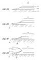
- FIGS. 1A-1Cschematically illustrate various embodiments of the present invention with an abutted junction structure.
- FIGS. 2A-2Fschematically illustrate an exemplary method of forming the MR read head with a continuous or abutted junction with a dusting layer directly below the underlayer.
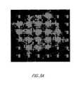
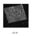
- FIG. 3Ais a 5 ⁇ m-by-5 ⁇ m atomic-force-microscopy (“AFM”) image of a 3-Angstrom-thick tungsten (W) dusting layer deposited on an aluminum oxide coating of a silicon substrate.
- AFMatomic-force-microscopy
- FIG. 3Bis a 5 ⁇ m-by-5 ⁇ m AFM image of a 7-Angstrom-thick W dusting layer on an aluminum oxide coating of a silicon substrate.
- FIG. 4Ais a 10 ⁇ m-by-10 ⁇ m magnetic-force-microscopy (“MFM”) image of a Si/Al 2 O 3 /70 ⁇ Cr/195 ⁇ CoPt structure.
- MFMmagnetic-force-microscopy
- FIG. 4Bis a 10 ⁇ m-by-10 ⁇ m MFM image of a Si/Al 2 O 3 /3 ⁇ W/70 ⁇ Cr/195 ⁇ CoPt structure.
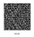
- FIG. 5Ais a 350 nm-by-350 nm plane-view transmission-electron-microscopy (“TEM”) image of a Si/Al 2 O 3 /70 ⁇ Cr/195 ⁇ CoPt structure.
- TEMtransmission-electron-microscopy
- FIG. 5Bis a 350 nm-by-350 nm plane-view TEM image of a Si/Al 2 O 3 /3 ⁇ W/70 ⁇ Cr/195 ⁇ CoPt structure.
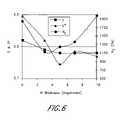
- FIG. 6is a vibrating sample magnetometer (“VSM”) measurement of the magnetic properties of a Si/Al 2 O 3 /W(t)/70 ⁇ Cr/195 ⁇ CoPt structure as a function of the thickness t of the grain size control W dusting layer.
- VSMvibrating sample magnetometer
- FIGS. 7A-7Dschematically illustrate an exemplary method of forming a continuous or abutted junction MR read head with a dusting layer directly below the HB layer.
- FIG. 8illustrates a VSM measurement of the magnetic properties of a Si/Al 2 O 3 /3 ⁇ W/70 ⁇ Cr/WTi(t)/195 ⁇ CoPt structure as a function of the thickness t of the WTi second dusting layer.
- FIG. 9is a 350 nm-by-350 nm plane-view TEM image of a Si/Al 2 O 3 /3 ⁇ W/70 ⁇ Cr/7 ⁇ WTi/195 ⁇ CoPt structure.
- FIGS. 1A-1Cschematically illustrate various embodiments of the present invention with an abutted junction structure.
- a magnetoresistive (“MR”) read head 10comprises a MR sensor 20 and a bias structure 30 adjacent to the MR sensor 20 .
- the bias structure 30provides a magnetostatic bias field for the MR sensor 20 .
- the bias structure 30comprises an underlayer 40 , a hard bias (“HB”) layer 50 over the underlayer 40 , and at least one dusting layer 60 a or 60 b .
- the dusting layer 60 a or 60 bis directly below at least one of the underlayer 40 or the HB layer 50 .
- the dusting layer 60 ais directly below the underlayer 40 .
- FIG. 1Athe dusting layer 60 a is directly below the underlayer 40 .
- FIG. 1Athe dusting layer 60 a is directly below the underlayer 40 .
- the dusting layer 60 bis directly below the HB layer 50 .
- a first dusting layer 60 ais directly below the underlayer 40 and a second dusting layer 60 b is directly below the HB layer 50 .
- the MR read head 10further comprises an electrically conductive lead layer 70 over the HB layer 50 .
- the MR sensor 20is selected from a group consisting of a giant magnetoresistive (GMR) sensor, an anisotropic magnetoresistive (AMR) sensor, a tunneling magnetoresistive (TMR) sensor, a spin-dependent-tunneling (SDT) sensor, a spin valve (SV) sensor, a current-in-plane (CIP) sensor, and a current-perpendicular-to-the-plane (CPP) sensor.
- GMRgiant magnetoresistive
- AMRanisotropic magnetoresistive
- TMRtunneling magnetoresistive
- SDTspin-dependent-tunneling
- SVspin valve
- CIPcurrent-in-plane
- CPPcurrent-perpendicular-to-the-plane
- the MR sensor 20comprises a dielectric layer 22 (e.g., aluminum oxide) formed on a substrate 23 (e.g., silicon), a pinning layer 24 over the dielectric layer 22 , a pinned layer 25 over the pinning layer 24 and antiferromagnetically coupled to the pinning layer 24 , a spacer layer 26 over the pinned layer 25 , a free layer 28 over the spacer layer 26 , and an overlayer 29 .
- the GMR-stack structure of the MR sensor 20 of FIG. 1Ais exemplary; other types and structures of MR sensors 20 are compatible with embodiments described herein.
- the underlayer 40comprises a material selected from a group consisting of chromium, chromium-containing alloy, tungsten, tungsten-containing alloy, nickel-aluminum alloy, and iron-aluminum alloy.
- the chromium-containing alloycan comprise a material selected from a group consisting of titanium, vanadium, molybdenum, manganese, and tungsten.
- the tungsten-containing alloycan comprise a material selected from a group consisting of chromium, titanium, vanadium, and molybdenum.
- the material of the underlayer 40 of certain embodimentsis selected to provide good lattice match with the material of the HB layer 50 (e.g., Cr underlayer 40 with a CoPt HB layer 50 ).
- the underlayer 40has a thickness in a range from approximately 20 Angstroms to approximately 250 Angstroms. In still other embodiments, the underlayer 40 has a thickness in a range from approximately 70 Angstroms to approximately 200 Angstroms. Other materials and thicknesses of the underlayer 40 are compatible with embodiments described herein.
- the HB layer 50comprises a material selected from a group consisting of CoPt, CoCrPt, CoCrPtTa, CoCrPtB, CrPt, CoPt, and FePt.
- the HB layer 50comprises a magnetic oxide (e.g., ferrous oxide).
- the material of the HB layer 50 of certain embodimentsis selected to provide a sufficiently high bias field to the MR sensor 20 to improve performance.
- the HB layer 50has a thickness in a range from approximately 75 Angstroms to approximately 300 Angstroms. In still other embodiments, the HB layer 50 has a thickness in a range from approximately 100 Angstroms to approximately 250 Angstroms. Other materials and thickness of the HB layer 50 are compatible with embodiments described herein.
- the MR read head 10comprises a dusting layer 60 a which is directly below the underlayer 40 .
- the dusting layer 60 a of certain embodimentscomprises discontinuous, densely-packed, small islands of material.
- the dusting layer 60 acomprises a material having a sufficiently high surface energy and a sufficiently low atomic mobility to form the islands.
- the dusting layer 60 acomprises a material having a body-centered-cubic crystallographic structure, while in other embodiments, the dusting layer 60 a comprises a material having a CsCl-type crystallographic structure.
- Exemplary materials for the dusting layer 60 acan be selected from the group consisting of tungsten, tantalum, niobium, rhodium, molybdenum, tungsten-titanium alloy, tungsten-chromium alloy, and nickel-aluminum alloy. Still other embodiments utilize a dusting layer 60 a comprising platinum or titanium.
- the dusting layer 60 a of certain embodimentscomprises a material having a melting temperature above the melting temperature of the underlayer 40 .
- the dusting layer 60 acomprises a material having a melting temperature above 1800 degrees Celsius.
- Such high melting point materialshave relatively high surface energy and low atomic mobility so as to form high density, nano-sized, island-like grains.
- Other materials for the dusting layer 60 aare compatible with embodiments described herein.
- the dusting layer 60 ahas a thickness less than approximately 10 Angstroms. In certain other embodiments, the dusting layer 60 a has a thickness in a range from approximately 2 Angstroms to approximately 6 Angstroms. In still other embodiments, the dusting layer 60 a has a thickness of approximately 3 Angstroms.
- the dusting layer 60 adiffers from multilayer underlayer structures, which have components which are significantly thicker (e.g., tens of Angstroms) than the dusting layer 60 a.
- FIGS. 2A-2Fschematically illustrate an exemplary method of forming a continuous or butted junction MR read head 10 with a dusting layer 60 a , as schematically illustrated by FIG. 1A .
- a MR sensor stack 110 having a dielectric layer 112 and a MR layer 113is first provided on a substrate 114 , as shown in FIG. 2A .
- the MR layer 113 of certain embodimentscomprises multiple layers, including the free layer 28 , as shown in FIG. 1A .
- the MR sensor stack 110is then patterned by etching or milling using a bi-layer (lift-off) photoresist mask. In certain embodiments, an ion-beam milling method is used to fabricate the MR sensor 20 .
- the ion-beam millingis controlled to stop in the dielectric layer 112 using end-point detection technique, as shown in FIG. 2B .
- the ion-beam millingcan be controlled to stop in another layer of the MR sensor stack 110 (e.g., PtMn, NiFe, CoFe).
- PtMne.g., NiFe, CoFe
- An exemplary method of ion-beam millingis described by U.S. Pat. No. 5,664,316 issued to Chen et al., which is incorporated in its entirety by reference herein.
- the structure shown FIG. 2B with a milled surface at the edge of the MR sensor 20is formed. Persons skilled in the art are able to use other methods of fabricating the MR sensor 20 in accordance with embodiments described herein.
- the dusting layer 60 ais then deposited on the milled surface of the MR sensor 20 , resulting in the structure shown in FIG. 2C .
- the dusting layer 60 a of certain embodimentscomprises discontinuous, densely-packed, small islands of material on the milled surface, as shown schematically in FIG. 2C .
- IBDion-beam deposition
- the dusting layer 60 ais relatively thin (e.g., approximately 3-6 Angstroms), the deposition rate is kept relatively low. For example, in certain embodiments using a IBD Model No. 350 tool from Veeco Instruments, Inc.
- the deposition energyis maintained to be approximately 650 Volts with a beam current of approximately 150 milliamps, thereby yielding a deposition rate of approximately 0.3 Angstroms/second.
- Other embodimentscan utilize other ion-beam-deposition tools (e.g., NEXUS IBD tool from Veeco Instruments, Inc.).
- the deposition of the dusting layer 60 ais performed at a deposition rate of approximately 0.3 Angstroms/second. In certain such embodiments, the deposition is performed for a time period having a duration ranging from approximately 8 seconds to approximately 30 seconds. In certain other embodiments, the deposition of the dusting layer 60 a is performed at a deposition rate of approximately 0.7 Angstroms/second. In certain such embodiments, the deposition is performed for a time period having a duration ranging from approximately 2 seconds to approximately 15 seconds.
- the underlayer 40is then deposited over the dusting layer 60 a , resulting in the structure shown in FIG. 2D .
- the HB layer 50is then deposited over the underlayer 40 , resulting in the structure shown in FIG. 2E .
- the underlayer 40establishes the desired c-axis in-plane orientation of the HB layer 50 .
- the center of the HB layer 50is approximately aligned with the free layer of the MR sensor 20 .
- the lead layer 70is deposited over the HB layer 50 , resulting in the structure shown in FIG. 2F .
- the lead layer 70comprises a conductive material (e.g., Au, W, Ph, Cr, Cu) with a range of thicknesses between about 100 Angstroms and about 1000 Angstroms thick.
- the lead layer 70provides the electrical connections to the MR sensor 20 for the sensing current.
- IBDis used to deposit the underlayer 40 , the HB layer 50 , and the lead layer 70 . Persons skilled in the art can select appropriate materials, thicknesses, and deposition parameters for these layers.
- the dusting layer 60 ainfluences the morphology (e.g., grain sizes) of the underlayer 40 deposited on the dusting layer 60 a .
- morphologye.g., grain sizes
- using the dusting layer 60 acan result in an underlayer 40 with small grain sizes, e.g., less than approximately 150 Angstroms.
- the dusting layer 60 acan also influence the morphology of the HB layer 50 deposited on the underlayer 40 .
- both the underlayer 40 and the HB layer 50can have grain sizes of approximately 100-110 Angstroms.
- the dusting layer 60 a and a thin underlayer 40the grain sizes of the HB layer 50 are affected by the dusting layer 60 a .
- the dusting layer 60 ais sometimes referred to as the “grain size control” dusting layer.
- the influence of the dusting layer 60 a on the grain sizes of the HB layer 50is more pronounced for thinner underlayers 40 and for dusting layers 60 a which are more island-like (e.g., less than 10 Angstroms in thickness).
- the island-like grains of the dusting layer 60 aare thought to act as nucleation sites for grain growth for the underlayer 40 , thereby significantly reducing the grain sizes of the underlayer 40 .
- the smaller grains of the underlayer 40are thought to then act as nucleation sites for grain growth for the HB layer 50 , thereby significantly reducing the grain sizes of the HB layer 50 .
- FIG. 3Ais an atomic-force-microscopy (“AFM”) image of a 3-Angstrom-thick tungsten (W) dusting layer 60 a deposited on an aluminum oxide coating of a silicon substrate.
- FIG. 3Bis an AFM image of a 7-Angstrom-thick W dusting layer 60 a on an aluminum oxide coating of a silicon substrate.
- Each of FIGS. 3A and 3Billustrates an approximately 5 microns by 5 microns square area of the W dusting layer 60 a .
- the morphology of the 3-Angstrom-thick W dusting layer 60 aincludes discrete W islands, as shown in FIG. 3A . As the thickness of the W dusting layer 60 a is increased to 7 Angstroms, as shown in FIG. 3B , more surface coverage of the dusting layer 60 a is formed, although it remains discontinuous.
- FIG. 4Ais a magnetic-force-microscopy (“MFM”) image of a 195-Angstrom-thick CoPt HB layer 50 on a 70-Angstrom-thick Cr underlayer 40 on an Al 2 O 3 dielectric layer 22 on a Si substrate 23 (denoted by Si/Al 2 O 3 /70 ⁇ Cr/195 ⁇ CoPt).
- FIG. 4Bis an MFM image of a similar structure, but with a 3-Angstrom-thick W dusting layer 60 a between the Al 2 O 3 dielectric layer 22 and the Cr underlayer 40 (denoted by Si/Al 2 O 3 /3 ⁇ W/70 ⁇ Cr/195 ⁇ CoPt).
- MFMmagnetic-force-microscopy
- FIG. 4A and 4Billustrates an approximately 10 microns by 10 microns square area of the HB layer 50 .
- Comparison of FIG. 4A and FIG. 4Billustrates that the HB layer 50 with the 3-Angstrom-thick W dusting layer 60 a exhibits smaller magnetic domain sizes, indicating the magnetic grain size reduction in the HB layer 50 resulting from the 3-Angstrom-thick dusting layer 60 a.
- FIG. 5Ais a plane-view transmission electron-microscopy (“TEM”) image of a 195-Angstrom-thick CoPt HB layer 50 on a 70-Angstrom-thick Cr underlayer 40 on an Al2O3 dielectric layer 22 on a Si substrate 23 (i.e., Si/Al2O3/70 ⁇ Cr/195 ⁇ CoPt).
- FIG. 5Bis a plane-view TEM image of a similar structure, but with a 3 Angstrom-thick W dusting layer 60 a between the Al2O3 dielectric layer 22 and the Cr underlayer 40 (i.e., Si/Al2O3/3 ⁇ W/70 ⁇ Cr/195 ⁇ CoPt).
- TEMtransmission electron-microscopy
- FIG. 5A and 5Billustrates an approximately 350 nanometers by 350 nanometers square area of the HB layer 50 .
- FIG. 5Aillustrates a polycrystalline grain structure with an average grain size of approximately 17.6 nanometers.
- FIG. 5Billustrates a much smaller grain size of approximately 10 nanometers.
- the W dusting layer 60 ahas improved the grain size uniformity, which is also desirable.
- the magnetic properties of the bias structure Si/Al 2 O 3 /W(t)/70 ⁇ Cr/195 ⁇ CoPt as a function of the thickness t of the grain size control W dusting layer 60 awere measured using a vibrating sample magnetometer (“VSM”), and the results are illustrated in FIG. 6 .
- the coercivity H cinitially decreases with increasing thickness of the W dusting layer 60 a , and reaches a minimum value at a thickness of approximately 3 Angstroms. Further increases of the thickness of the W dusting layer 60 a to a thickness of approximately 10 Angstroms result in a rebound of H c , reaching the same value as in a film without the W dusting layer 60 a . While the dusting layer 60 a reduces the grain sizes of the HB layer 50 , it also reduces the coercivity of the HB layer 50 .
- TEM studiesindicate that the increase of H c at thicker W dusting layers 60 a is accompanied by an increase in the grain size of the CoPt HB layer 50 , possibly due to the diminishing effect of the grain size control dusting layer 60 a .
- Other embodiments using dual dusting layers 60 a , 60 bcan be used to obtain high H c while maintaining the small grain size achieved by using the grain size control dusting layer 60 a , as described in more detail below.
- FIG. 1Bschematically illustrates another embodiment in which the MR read head 10 comprises a dusting layer 60 b which is directly below the HB layer 50 .
- the dusting layer 60 b of certain embodimentscomprises discontinuous, densely-packed, small islands of material.
- the dusting layer 60 bcomprises a material having a sufficiently high surface energy and a sufficiently low atomic mobility to form the islands.
- the dusting layer 60 bis a continuous layer with good lattice match to both the underlayer 40 and the HB layer 50 .
- the dusting layer 60 bcomprises a material having a body-centered-cubic crystallographic structure, while in other embodiments, the dusting layer 60 b comprises a material having a CsCl-type crystallographic structure.
- Exemplary materials for the dusting layer 60 bcan be selected from the group consisting of tungsten, tantalum, niobium, rhodium, molybdenum, tungsten-containing alloy, chromium-containing alloy, tungsten-titanium alloy, tungsten-chromium alloy, and nickel-aluminum alloy.
- the dusting layer 60 b of certain embodimentscomprises a material having a melting temperature above the melting temperature of the underlayer 40 .
- the dusting layer 60 bcomprises a material having a melting temperature above 1800 degrees Celsius.
- Such high melting point materialshave relatively high surface energy and low atomic mobility so as to form high density, nano-sized, island-like grains.
- Other materials for the dusting layer 60 bare compatible with embodiments described herein.
- the dusting layer 60 bhas a thickness less than approximately 10 Angstroms. In certain other embodiments, the dusting layer 60 b has a thickness in a range from approximately 5 Angstroms to approximately 10 Angstroms. In still other embodiments, the dusting layer 60 b has a thickness of approximately 7 Angstroms.
- the dusting layer 60 bdiffers from multilayer underlayer structures, which have components which are significantly thicker (e.g., tens of Angstroms) than the dusting layer 60 b.
- FIGS. 7A-7Dschematically illustrate an exemplary method of forming a continuous or abutted junction MR read head 10 with the dusting layer 60 b , as schematically illustrated by FIG. 1B .
- FIG. 7Aschematically illustrates a patterned MR sensor 20 which is the same as that shown in FIG. 2B , and can be formed using the same techniques as described above in relation to FIG. 2B .
- Persons skilled in the artare able to use other methods of fabricating the MR sensor 20 in accordance with embodiments described herein.
- the underlayer 40is deposited on the milled surface of the MR sensor 20 , resulting in the structure shown in FIG. 7B .
- the dusting layer 60 bis then deposited on the underlayer 40 , resulting in the structure shown in FIG. 7C .
- the dusting layer 60 b of certain embodimentscomprises discontinuous, densely-packed, small islands of material on the underlayer 40 , as shown schematically in FIG. 7C .
- the dusting layer 60 bis a continuous layer with good lattice match to both the underlayer 40 and the HB layer 50 .
- the dusting layer 60 b of certain embodimentsis deposited on the underlayer 40 using IBD techniques. If the thickness of the dusting layer 60 b is above 10 Angstroms, the dusting layer 60 b becomes less island-like and more continuous, so the thickness of the dusting layer 60 b is preferably carefully monitored.
- the deposition of the dusting layer 60 bis performed at a deposition rate of approximately 0.3 Angstroms/second. In certain such embodiments, the deposition is performed for a time period having a duration ranging from approximately 15 seconds to approximately 30 seconds. In certain other embodiments, the deposition of the dusting layer 60 b is performed at a deposition rate of approximately 0.7 Angstroms/second. In certain such embodiments, the deposition is performed for a time period having a duration ranging from approximately 7 seconds to approximately 15 seconds.
- the HB layer 50is then deposited over the dusting layer 60 b .
- the center of the HB layer 50is approximately aligned with the free layer of the MR sensor 20 .
- the lead layer 70is deposited over the HB layer 50 , resulting in the structure shown in FIG. 7D .
- IBDis used to deposit the underlayer 40 , the HB layer 50 , and the lead layer 70 . Persons skilled in the art can select appropriate materials, thicknesses, and deposition parameters for these layers.
- the dusting layer 60 binfluences the morphology (e.g., texture) of the HB layer 50 deposited on the dusting layer 60 b .
- the dusting layer 60 bis sometimes referred to as the “texture control” dusting layer.
- the texture control dusting layer 60 bmodifies the crystallography of the HB layer 50 by inducing better in-plane texture and thus higher coercivity due to better lattice match between the dusting layer 60 b and the HB layer 50 . Due to the small thickness of the dusting layer 60 b , the higher coercivity is achieved without significant penalty of increasing grain size in the HB layer 50 .
- the dusting layer 60 bhas an island-like structure
- the islandsact as nucleation sites for grain growth for the HB layer 50 .
- the lattice of the dusting layer 60 bas a template for growth of the HB layer 50 .
- embodiments utilizing the grain size control dusting layer 60 a aloneproduce small grain sizes in the HB layer 50 , and a corresponding reduction of the coercivity H c .
- embodiments utilizing the texture control dusting layer 60 b directly below the HB layer 50 in conjunction with the grain size control dusting layer 60 a directly below the underlayer 40can maintain relatively small grain sizes while achieving higher coercivities H c .
- One embodiment of such a bias structure 40is shown schematically in FIG. 1C .
- Such embodimentscan be fabricated by an exemplary method which combines the two processes outlined by FIGS. 2A-2F and FIGS. 7A-7D .
- the first dusting layer 60 ais deposited on the milled surface.
- the underlayer 40is then deposited on the first dusting layer 60 a
- the second dusting layer 60 bis deposited on the underlayer 40 .
- the HB layer 50is then deposited on the second dusting layer 60 b
- the lead layer 70is deposited on the HB layer 50 .
- the first dusting layer 60 a and the second dusting layer 60 bcomprise the same material, while in other embodiments, the two dusting layers 60 a and 60 b comprise different materials.
- Persons skilled in the artcan select appropriate materials, thicknesses and deposition parameters for the various layers.
- the grain sizes of the HB layer 50 and of the underlayer 40are substantially the same (e.g. 100-110 Angstroms). However, in embodiments which also use the texture control dusting layer 60 b , the grain sizes of the HB layer 50 are increased (e.g., 140-150 Angstroms) to be larger than the grain sizes of the underlayer 40 (e.g., 100-110 Angstroms). Thus, in certain embodiments, the bias layer has an average grain size which is larger than an average grain size of the underlayer 40 .
- FIG. 8illustrates the VSM-measured magnetic properties of such a bias structure 30 with the two dusting layers 60 a , 60 b .
- the bias structure 30comprises a 3-Angstrom-thick W first dusting layer 60 a deposited on Al 2 O 3 , a 70-Angstrom-thick Cr underlayer 40 deposited on the first dusting layer 60 a , a WTi second dusting layer 60 b deposited on the underlayer 40 , and a 195-Angstrom-thick CoPt HB layer 50 deposited on the second dusting layer 60 b (i.e., Si/Al 2 O 3 /3 ⁇ W/70 ⁇ Cr/WTi(t)/195 ⁇ CoPt) as a function of the thickness t of the WTi second dusting layer 60 b .
- H cis improved from 1100 Oersteds to about 2400 Oersteds with a WTi thickness of approximately 5 Angstroms.
- Such improvementis attributable to better lattice matching between the WTi (with an atomic percentage of Ti of approximately 20%) and the CoPt (with an atomic percentage of Pt of approximately 20%).
- FIG. 9illustrates a 350-nanometer-by-350-nanometer plane-view TEM image of the grains of a bias structure 30 with a 3-Angstrom-thick W first dusting layer 60 a and a 7-Angstrom-thick WTi second dusting layer 60 b (i.e. Si/Al 2 O 3 /3 ⁇ W/70 ⁇ Cr/7 ⁇ WTi/195 ⁇ CoPt).
- FIG. 9shows an average grain size, calculated from the dark field image, of approximately 14 nanometers, which is 30% smaller than that of a conventional HB layer 50 with a 70-Angstrom-thick Cr Linderlayer 40 and a 195-Angstrom-thick CoPt HB layer 50 .
- the coercivity H cis approximately 40% higher than that of the conventional structure, indicating the benefit of using the two dusting layers 60 a , 60 b .
- the grain size of the HB layer 50is decreased while maintaining a high coercivity H c .
- Certain embodimentsare particularly useful for minimizing the effects of NNJ on amplitude, asymmetry, and other properties of the MR sensor 10 . Certain embodiments are also used to suppress hard-bias-related magnetic noise, thereby enhancing the signal-to-noise ratio of the read head.
Landscapes
- Engineering & Computer Science (AREA)
- Chemical & Material Sciences (AREA)
- Nanotechnology (AREA)
- Crystallography & Structural Chemistry (AREA)
- Manufacturing & Machinery (AREA)
- Physics & Mathematics (AREA)
- Mathematical Physics (AREA)
- Theoretical Computer Science (AREA)
- Magnetic Heads (AREA)
Abstract
Description
Claims (36)
Priority Applications (2)
| Application Number | Priority Date | Filing Date | Title |
|---|---|---|---|
| US10/769,239US7342752B1 (en) | 2004-01-31 | 2004-01-31 | Magnetoresistive read head having a bias structure with at least one dusting layer |
| US11/971,398US7691434B1 (en) | 2004-01-31 | 2008-01-09 | Method for fabricating magnetoresistive read head having a bias structure with at least one dusting layer |
Applications Claiming Priority (1)
| Application Number | Priority Date | Filing Date | Title |
|---|---|---|---|
| US10/769,239US7342752B1 (en) | 2004-01-31 | 2004-01-31 | Magnetoresistive read head having a bias structure with at least one dusting layer |
Related Child Applications (1)
| Application Number | Title | Priority Date | Filing Date |
|---|---|---|---|
| US11/971,398DivisionUS7691434B1 (en) | 2004-01-31 | 2008-01-09 | Method for fabricating magnetoresistive read head having a bias structure with at least one dusting layer |
Publications (1)
| Publication Number | Publication Date |
|---|---|
| US7342752B1true US7342752B1 (en) | 2008-03-11 |
Family
ID=39155375
Family Applications (2)
| Application Number | Title | Priority Date | Filing Date |
|---|---|---|---|
| US10/769,239Expired - Fee RelatedUS7342752B1 (en) | 2004-01-31 | 2004-01-31 | Magnetoresistive read head having a bias structure with at least one dusting layer |
| US11/971,398Expired - Fee RelatedUS7691434B1 (en) | 2004-01-31 | 2008-01-09 | Method for fabricating magnetoresistive read head having a bias structure with at least one dusting layer |
Family Applications After (1)
| Application Number | Title | Priority Date | Filing Date |
|---|---|---|---|
| US11/971,398Expired - Fee RelatedUS7691434B1 (en) | 2004-01-31 | 2008-01-09 | Method for fabricating magnetoresistive read head having a bias structure with at least one dusting layer |
Country Status (1)
| Country | Link |
|---|---|
| US (2) | US7342752B1 (en) |
Cited By (136)
| Publication number | Priority date | Publication date | Assignee | Title |
|---|---|---|---|---|
| US20060222112A1 (en)* | 2005-03-31 | 2006-10-05 | Hitachi Global Storage Technologies | Magnetic read sensor employing oblique etched underlayers for inducing uniaxial magnetic anisotropy in hard magnetic bias layers |
| US7639457B1 (en)* | 2004-02-27 | 2009-12-29 | Western Digital (Fremont), Llc | Magnetic sensor with underlayers promoting high-coercivity, in-plane bias layers |
| US7672090B2 (en) | 2005-03-31 | 2010-03-02 | Hitachi Global Storage Technologies Netherlands B.V. | Magnetic read sensor employing oblique etched underlayers for inducing uniaxial magnetic anisotropy in a hard magnetic pinning layer |
| US20110235216A1 (en)* | 2010-03-26 | 2011-09-29 | Tsann Lin | Longitudinal bias stack for a current-perpendicular-to-plane (cpp) read sensor |
| US8339753B1 (en)* | 2011-10-11 | 2012-12-25 | Hitachi Global Storage Technologies Netherlands B.V. | Magnetic bias structure for magnetoresistive sensor |
| US8385025B2 (en) | 2010-12-15 | 2013-02-26 | HGST Netherlands B.V. | Current-perpendicular-to-the-plane (CPP) magnetoresistive (MR) sensor with improved seed layer structure for hard bias layer |
| US8830628B1 (en) | 2009-02-23 | 2014-09-09 | Western Digital (Fremont), Llc | Method and system for providing a perpendicular magnetic recording head |
| US8879207B1 (en) | 2011-12-20 | 2014-11-04 | Western Digital (Fremont), Llc | Method for providing a side shield for a magnetic recording transducer using an air bridge |
| US8883017B1 (en) | 2013-03-12 | 2014-11-11 | Western Digital (Fremont), Llc | Method and system for providing a read transducer having seamless interfaces |
| US8917581B1 (en) | 2013-12-18 | 2014-12-23 | Western Digital Technologies, Inc. | Self-anneal process for a near field transducer and chimney in a hard disk drive assembly |
| US8923102B1 (en) | 2013-07-16 | 2014-12-30 | Western Digital (Fremont), Llc | Optical grating coupling for interferometric waveguides in heat assisted magnetic recording heads |
| US8947985B1 (en) | 2013-07-16 | 2015-02-03 | Western Digital (Fremont), Llc | Heat assisted magnetic recording transducers having a recessed pole |
| US8953422B1 (en) | 2014-06-10 | 2015-02-10 | Western Digital (Fremont), Llc | Near field transducer using dielectric waveguide core with fine ridge feature |
| US8958272B1 (en) | 2014-06-10 | 2015-02-17 | Western Digital (Fremont), Llc | Interfering near field transducer for energy assisted magnetic recording |
| US8970988B1 (en) | 2013-12-31 | 2015-03-03 | Western Digital (Fremont), Llc | Electric gaps and method for making electric gaps for multiple sensor arrays |
| US8971160B1 (en) | 2013-12-19 | 2015-03-03 | Western Digital (Fremont), Llc | Near field transducer with high refractive index pin for heat assisted magnetic recording |
| US8976635B1 (en) | 2014-06-10 | 2015-03-10 | Western Digital (Fremont), Llc | Near field transducer driven by a transverse electric waveguide for energy assisted magnetic recording |
| US8980109B1 (en) | 2012-12-11 | 2015-03-17 | Western Digital (Fremont), Llc | Method for providing a magnetic recording transducer using a combined main pole and side shield CMP for a wraparound shield scheme |
| US8982508B1 (en) | 2011-10-31 | 2015-03-17 | Western Digital (Fremont), Llc | Method for providing a side shield for a magnetic recording transducer |
| US8984740B1 (en) | 2012-11-30 | 2015-03-24 | Western Digital (Fremont), Llc | Process for providing a magnetic recording transducer having a smooth magnetic seed layer |
| US8988825B1 (en) | 2014-02-28 | 2015-03-24 | Western Digital (Fremont, LLC | Method for fabricating a magnetic writer having half-side shields |
| US8988812B1 (en) | 2013-11-27 | 2015-03-24 | Western Digital (Fremont), Llc | Multi-sensor array configuration for a two-dimensional magnetic recording (TDMR) operation |
| US8993217B1 (en) | 2013-04-04 | 2015-03-31 | Western Digital (Fremont), Llc | Double exposure technique for high resolution disk imaging |
| US8995087B1 (en) | 2006-11-29 | 2015-03-31 | Western Digital (Fremont), Llc | Perpendicular magnetic recording write head having a wrap around shield |
| US9001628B1 (en) | 2013-12-16 | 2015-04-07 | Western Digital (Fremont), Llc | Assistant waveguides for evaluating main waveguide coupling efficiency and diode laser alignment tolerances for hard disk |
| US9001467B1 (en) | 2014-03-05 | 2015-04-07 | Western Digital (Fremont), Llc | Method for fabricating side shields in a magnetic writer |
| US8997832B1 (en) | 2010-11-23 | 2015-04-07 | Western Digital (Fremont), Llc | Method of fabricating micrometer scale components |
| US9007879B1 (en) | 2014-06-10 | 2015-04-14 | Western Digital (Fremont), Llc | Interfering near field transducer having a wide metal bar feature for energy assisted magnetic recording |
| US9007719B1 (en) | 2013-10-23 | 2015-04-14 | Western Digital (Fremont), Llc | Systems and methods for using double mask techniques to achieve very small features |
| US9007725B1 (en) | 2014-10-07 | 2015-04-14 | Western Digital (Fremont), Llc | Sensor with positive coupling between dual ferromagnetic free layer laminates |
| US9013836B1 (en) | 2013-04-02 | 2015-04-21 | Western Digital (Fremont), Llc | Method and system for providing an antiferromagnetically coupled return pole |
| US9042208B1 (en) | 2013-03-11 | 2015-05-26 | Western Digital Technologies, Inc. | Disk drive measuring fly height by applying a bias voltage to an electrically insulated write component of a head |
| US9042057B1 (en) | 2013-01-09 | 2015-05-26 | Western Digital (Fremont), Llc | Methods for providing magnetic storage elements with high magneto-resistance using Heusler alloys |
| US9042051B2 (en) | 2013-08-15 | 2015-05-26 | Western Digital (Fremont), Llc | Gradient write gap for perpendicular magnetic recording writer |
| US9042052B1 (en) | 2014-06-23 | 2015-05-26 | Western Digital (Fremont), Llc | Magnetic writer having a partially shunted coil |
| US9042058B1 (en) | 2013-10-17 | 2015-05-26 | Western Digital Technologies, Inc. | Shield designed for middle shields in a multiple sensor array |
| US9053735B1 (en) | 2014-06-20 | 2015-06-09 | Western Digital (Fremont), Llc | Method for fabricating a magnetic writer using a full-film metal planarization |
| US9064528B1 (en) | 2013-05-17 | 2015-06-23 | Western Digital Technologies, Inc. | Interferometric waveguide usable in shingled heat assisted magnetic recording in the absence of a near-field transducer |
| US9065043B1 (en) | 2012-06-29 | 2015-06-23 | Western Digital (Fremont), Llc | Tunnel magnetoresistance read head with narrow shield-to-shield spacing |
| US9064527B1 (en) | 2013-04-12 | 2015-06-23 | Western Digital (Fremont), Llc | High order tapered waveguide for use in a heat assisted magnetic recording head |
| US9064507B1 (en) | 2009-07-31 | 2015-06-23 | Western Digital (Fremont), Llc | Magnetic etch-stop layer for magnetoresistive read heads |
| US9070381B1 (en) | 2013-04-12 | 2015-06-30 | Western Digital (Fremont), Llc | Magnetic recording read transducer having a laminated free layer |
| US9082423B1 (en) | 2013-12-18 | 2015-07-14 | Western Digital (Fremont), Llc | Magnetic recording write transducer having an improved trailing surface profile |
| US9087527B1 (en) | 2014-10-28 | 2015-07-21 | Western Digital (Fremont), Llc | Apparatus and method for middle shield connection in magnetic recording transducers |
| US9087534B1 (en) | 2011-12-20 | 2015-07-21 | Western Digital (Fremont), Llc | Method and system for providing a read transducer having soft and hard magnetic bias structures |
| US9093639B2 (en) | 2012-02-21 | 2015-07-28 | Western Digital (Fremont), Llc | Methods for manufacturing a magnetoresistive structure utilizing heating and cooling |
| US9104107B1 (en) | 2013-04-03 | 2015-08-11 | Western Digital (Fremont), Llc | DUV photoresist process |
| US9111550B1 (en) | 2014-12-04 | 2015-08-18 | Western Digital (Fremont), Llc | Write transducer having a magnetic buffer layer spaced between a side shield and a write pole by non-magnetic layers |
| US9111558B1 (en) | 2014-03-14 | 2015-08-18 | Western Digital (Fremont), Llc | System and method of diffractive focusing of light in a waveguide |
| US9111564B1 (en) | 2013-04-02 | 2015-08-18 | Western Digital (Fremont), Llc | Magnetic recording writer having a main pole with multiple flare angles |
| US9123358B1 (en) | 2012-06-11 | 2015-09-01 | Western Digital (Fremont), Llc | Conformal high moment side shield seed layer for perpendicular magnetic recording writer |
| US9123362B1 (en) | 2011-03-22 | 2015-09-01 | Western Digital (Fremont), Llc | Methods for assembling an electrically assisted magnetic recording (EAMR) head |
| US9123374B1 (en) | 2015-02-12 | 2015-09-01 | Western Digital (Fremont), Llc | Heat assisted magnetic recording writer having an integrated polarization rotation plate |
| US9123359B1 (en) | 2010-12-22 | 2015-09-01 | Western Digital (Fremont), Llc | Magnetic recording transducer with sputtered antiferromagnetic coupling trilayer between plated ferromagnetic shields and method of fabrication |
| US9135930B1 (en) | 2014-03-06 | 2015-09-15 | Western Digital (Fremont), Llc | Method for fabricating a magnetic write pole using vacuum deposition |
| US9135937B1 (en) | 2014-05-09 | 2015-09-15 | Western Digital (Fremont), Llc | Current modulation on laser diode for energy assisted magnetic recording transducer |
| US9142233B1 (en) | 2014-02-28 | 2015-09-22 | Western Digital (Fremont), Llc | Heat assisted magnetic recording writer having a recessed pole |
| US9147408B1 (en) | 2013-12-19 | 2015-09-29 | Western Digital (Fremont), Llc | Heated AFM layer deposition and cooling process for TMR magnetic recording sensor with high pinning field |
| US9147404B1 (en) | 2015-03-31 | 2015-09-29 | Western Digital (Fremont), Llc | Method and system for providing a read transducer having a dual free layer |
| US9153255B1 (en) | 2014-03-05 | 2015-10-06 | Western Digital (Fremont), Llc | Method for fabricating a magnetic writer having an asymmetric gap and shields |
| US9183854B2 (en) | 2014-02-24 | 2015-11-10 | Western Digital (Fremont), Llc | Method to make interferometric taper waveguide for HAMR light delivery |
| US9190079B1 (en) | 2014-09-22 | 2015-11-17 | Western Digital (Fremont), Llc | Magnetic write pole having engineered radius of curvature and chisel angle profiles |
| US9190085B1 (en) | 2014-03-12 | 2015-11-17 | Western Digital (Fremont), Llc | Waveguide with reflective grating for localized energy intensity |
| US9194692B1 (en) | 2013-12-06 | 2015-11-24 | Western Digital (Fremont), Llc | Systems and methods for using white light interferometry to measure undercut of a bi-layer structure |
| US9202480B2 (en) | 2009-10-14 | 2015-12-01 | Western Digital (Fremont), LLC. | Double patterning hard mask for damascene perpendicular magnetic recording (PMR) writer |
| US9202493B1 (en) | 2014-02-28 | 2015-12-01 | Western Digital (Fremont), Llc | Method of making an ultra-sharp tip mode converter for a HAMR head |
| US9214172B2 (en) | 2013-10-23 | 2015-12-15 | Western Digital (Fremont), Llc | Method of manufacturing a magnetic read head |
| US9214165B1 (en) | 2014-12-18 | 2015-12-15 | Western Digital (Fremont), Llc | Magnetic writer having a gradient in saturation magnetization of the shields |
| US9213322B1 (en) | 2012-08-16 | 2015-12-15 | Western Digital (Fremont), Llc | Methods for providing run to run process control using a dynamic tuner |
| US9214169B1 (en) | 2014-06-20 | 2015-12-15 | Western Digital (Fremont), Llc | Magnetic recording read transducer having a laminated free layer |
| US9230565B1 (en) | 2014-06-24 | 2016-01-05 | Western Digital (Fremont), Llc | Magnetic shield for magnetic recording head |
| US9236560B1 (en) | 2014-12-08 | 2016-01-12 | Western Digital (Fremont), Llc | Spin transfer torque tunneling magnetoresistive device having a laminated free layer with perpendicular magnetic anisotropy |
| US9245545B1 (en) | 2013-04-12 | 2016-01-26 | Wester Digital (Fremont), Llc | Short yoke length coils for magnetic heads in disk drives |
| US9245562B1 (en) | 2015-03-30 | 2016-01-26 | Western Digital (Fremont), Llc | Magnetic recording writer with a composite main pole |
| US9245543B1 (en) | 2010-06-25 | 2016-01-26 | Western Digital (Fremont), Llc | Method for providing an energy assisted magnetic recording head having a laser integrally mounted to the slider |
| US9251813B1 (en) | 2009-04-19 | 2016-02-02 | Western Digital (Fremont), Llc | Method of making a magnetic recording head |
| US9263067B1 (en) | 2013-05-29 | 2016-02-16 | Western Digital (Fremont), Llc | Process for making PMR writer with constant side wall angle |
| US9263071B1 (en) | 2015-03-31 | 2016-02-16 | Western Digital (Fremont), Llc | Flat NFT for heat assisted magnetic recording |
| US9269382B1 (en) | 2012-06-29 | 2016-02-23 | Western Digital (Fremont), Llc | Method and system for providing a read transducer having improved pinning of the pinned layer at higher recording densities |
| US9275657B1 (en) | 2013-08-14 | 2016-03-01 | Western Digital (Fremont), Llc | Process for making PMR writer with non-conformal side gaps |
| US9280990B1 (en) | 2013-12-11 | 2016-03-08 | Western Digital (Fremont), Llc | Method for fabricating a magnetic writer using multiple etches |
| US9287494B1 (en) | 2013-06-28 | 2016-03-15 | Western Digital (Fremont), Llc | Magnetic tunnel junction (MTJ) with a magnesium oxide tunnel barrier |
| US9286919B1 (en) | 2014-12-17 | 2016-03-15 | Western Digital (Fremont), Llc | Magnetic writer having a dual side gap |
| US9305583B1 (en) | 2014-02-18 | 2016-04-05 | Western Digital (Fremont), Llc | Method for fabricating a magnetic writer using multiple etches of damascene materials |
| US9312064B1 (en) | 2015-03-02 | 2016-04-12 | Western Digital (Fremont), Llc | Method to fabricate a magnetic head including ion milling of read gap using dual layer hard mask |
| US9318130B1 (en) | 2013-07-02 | 2016-04-19 | Western Digital (Fremont), Llc | Method to fabricate tunneling magnetic recording heads with extended pinned layer |
| US9336814B1 (en) | 2013-03-12 | 2016-05-10 | Western Digital (Fremont), Llc | Inverse tapered waveguide for use in a heat assisted magnetic recording head |
| US9343098B1 (en) | 2013-08-23 | 2016-05-17 | Western Digital (Fremont), Llc | Method for providing a heat assisted magnetic recording transducer having protective pads |
| US9343087B1 (en) | 2014-12-21 | 2016-05-17 | Western Digital (Fremont), Llc | Method for fabricating a magnetic writer having half shields |
| US9343086B1 (en) | 2013-09-11 | 2016-05-17 | Western Digital (Fremont), Llc | Magnetic recording write transducer having an improved sidewall angle profile |
| US9349394B1 (en) | 2013-10-18 | 2016-05-24 | Western Digital (Fremont), Llc | Method for fabricating a magnetic writer having a gradient side gap |
| US9349392B1 (en) | 2012-05-24 | 2016-05-24 | Western Digital (Fremont), Llc | Methods for improving adhesion on dielectric substrates |
| US9361913B1 (en) | 2013-06-03 | 2016-06-07 | Western Digital (Fremont), Llc | Recording read heads with a multi-layer AFM layer methods and apparatuses |
| US9361914B1 (en) | 2014-06-18 | 2016-06-07 | Western Digital (Fremont), Llc | Magnetic sensor with thin capping layer |
| US9368134B1 (en) | 2010-12-16 | 2016-06-14 | Western Digital (Fremont), Llc | Method and system for providing an antiferromagnetically coupled writer |
| US9384763B1 (en) | 2015-03-26 | 2016-07-05 | Western Digital (Fremont), Llc | Dual free layer magnetic reader having a rear bias structure including a soft bias layer |
| US9384765B1 (en) | 2015-09-24 | 2016-07-05 | Western Digital (Fremont), Llc | Method and system for providing a HAMR writer having improved optical efficiency |
| US9396743B1 (en) | 2014-02-28 | 2016-07-19 | Western Digital (Fremont), Llc | Systems and methods for controlling soft bias thickness for tunnel magnetoresistance readers |
| US9396742B1 (en) | 2012-11-30 | 2016-07-19 | Western Digital (Fremont), Llc | Magnetoresistive sensor for a magnetic storage system read head, and fabrication method thereof |
| US9406331B1 (en) | 2013-06-17 | 2016-08-02 | Western Digital (Fremont), Llc | Method for making ultra-narrow read sensor and read transducer device resulting therefrom |
| US9424866B1 (en) | 2015-09-24 | 2016-08-23 | Western Digital (Fremont), Llc | Heat assisted magnetic recording write apparatus having a dielectric gap |
| US9431032B1 (en) | 2013-08-14 | 2016-08-30 | Western Digital (Fremont), Llc | Electrical connection arrangement for a multiple sensor array usable in two-dimensional magnetic recording |
| US9431038B1 (en) | 2015-06-29 | 2016-08-30 | Western Digital (Fremont), Llc | Method for fabricating a magnetic write pole having an improved sidewall angle profile |
| US9431047B1 (en) | 2013-05-01 | 2016-08-30 | Western Digital (Fremont), Llc | Method for providing an improved AFM reader shield |
| US9431031B1 (en) | 2015-03-24 | 2016-08-30 | Western Digital (Fremont), Llc | System and method for magnetic transducers having multiple sensors and AFC shields |
| US9431039B1 (en) | 2013-05-21 | 2016-08-30 | Western Digital (Fremont), Llc | Multiple sensor array usable in two-dimensional magnetic recording |
| US9437251B1 (en) | 2014-12-22 | 2016-09-06 | Western Digital (Fremont), Llc | Apparatus and method having TDMR reader to reader shunts |
| US9441938B1 (en) | 2013-10-08 | 2016-09-13 | Western Digital (Fremont), Llc | Test structures for measuring near field transducer disc length |
| US9443541B1 (en) | 2015-03-24 | 2016-09-13 | Western Digital (Fremont), Llc | Magnetic writer having a gradient in saturation magnetization of the shields and return pole |
| US9449621B1 (en) | 2015-03-26 | 2016-09-20 | Western Digital (Fremont), Llc | Dual free layer magnetic reader having a rear bias structure having a high aspect ratio |
| US9449625B1 (en) | 2014-12-24 | 2016-09-20 | Western Digital (Fremont), Llc | Heat assisted magnetic recording head having a plurality of diffusion barrier layers |
| US9472216B1 (en) | 2015-09-23 | 2016-10-18 | Western Digital (Fremont), Llc | Differential dual free layer magnetic reader |
| US9484051B1 (en) | 2015-11-09 | 2016-11-01 | The Provost, Fellows, Foundation Scholars and the other members of Board, of the College of the Holy and Undivided Trinity of Queen Elizabeth near Dublin | Method and system for reducing undesirable reflections in a HAMR write apparatus |
| US9508372B1 (en) | 2015-06-03 | 2016-11-29 | Western Digital (Fremont), Llc | Shingle magnetic writer having a low sidewall angle pole |
| US9508363B1 (en) | 2014-06-17 | 2016-11-29 | Western Digital (Fremont), Llc | Method for fabricating a magnetic write pole having a leading edge bevel |
| US9508365B1 (en) | 2015-06-24 | 2016-11-29 | Western Digital (Fremont), LLC. | Magnetic reader having a crystal decoupling structure |
| US9530443B1 (en) | 2015-06-25 | 2016-12-27 | Western Digital (Fremont), Llc | Method for fabricating a magnetic recording device having a high aspect ratio structure |
| US9564150B1 (en) | 2015-11-24 | 2017-02-07 | Western Digital (Fremont), Llc | Magnetic read apparatus having an improved read sensor isolation circuit |
| US9595273B1 (en) | 2015-09-30 | 2017-03-14 | Western Digital (Fremont), Llc | Shingle magnetic writer having nonconformal shields |
| US9646639B2 (en) | 2015-06-26 | 2017-05-09 | Western Digital (Fremont), Llc | Heat assisted magnetic recording writer having integrated polarization rotation waveguides |
| US9666214B1 (en) | 2015-09-23 | 2017-05-30 | Western Digital (Fremont), Llc | Free layer magnetic reader that may have a reduced shield-to-shield spacing |
| US9721595B1 (en) | 2014-12-04 | 2017-08-01 | Western Digital (Fremont), Llc | Method for providing a storage device |
| US9740805B1 (en) | 2015-12-01 | 2017-08-22 | Western Digital (Fremont), Llc | Method and system for detecting hotspots for photolithographically-defined devices |
| US9741366B1 (en) | 2014-12-18 | 2017-08-22 | Western Digital (Fremont), Llc | Method for fabricating a magnetic writer having a gradient in saturation magnetization of the shields |
| US9754611B1 (en) | 2015-11-30 | 2017-09-05 | Western Digital (Fremont), Llc | Magnetic recording write apparatus having a stepped conformal trailing shield |
| US9767831B1 (en) | 2015-12-01 | 2017-09-19 | Western Digital (Fremont), Llc | Magnetic writer having convex trailing surface pole and conformal write gap |
| US9786301B1 (en) | 2014-12-02 | 2017-10-10 | Western Digital (Fremont), Llc | Apparatuses and methods for providing thin shields in a multiple sensor array |
| US9799351B1 (en) | 2015-11-30 | 2017-10-24 | Western Digital (Fremont), Llc | Short yoke length writer having assist coils |
| US9812155B1 (en) | 2015-11-23 | 2017-11-07 | Western Digital (Fremont), Llc | Method and system for fabricating high junction angle read sensors |
| US9842615B1 (en) | 2015-06-26 | 2017-12-12 | Western Digital (Fremont), Llc | Magnetic reader having a nonmagnetic insertion layer for the pinning layer |
| US9858951B1 (en) | 2015-12-01 | 2018-01-02 | Western Digital (Fremont), Llc | Method for providing a multilayer AFM layer in a read sensor |
| US9881638B1 (en) | 2014-12-17 | 2018-01-30 | Western Digital (Fremont), Llc | Method for providing a near-field transducer (NFT) for a heat assisted magnetic recording (HAMR) device |
| US9934811B1 (en) | 2014-03-07 | 2018-04-03 | Western Digital (Fremont), Llc | Methods for controlling stray fields of magnetic features using magneto-elastic anisotropy |
| US9953670B1 (en) | 2015-11-10 | 2018-04-24 | Western Digital (Fremont), Llc | Method and system for providing a HAMR writer including a multi-mode interference device |
| US10037770B1 (en) | 2015-11-12 | 2018-07-31 | Western Digital (Fremont), Llc | Method for providing a magnetic recording write apparatus having a seamless pole |
| US10074387B1 (en) | 2014-12-21 | 2018-09-11 | Western Digital (Fremont), Llc | Method and system for providing a read transducer having symmetric antiferromagnetically coupled shields |
Families Citing this family (1)
| Publication number | Priority date | Publication date | Assignee | Title |
|---|---|---|---|---|
| US9099126B2 (en) | 2013-07-30 | 2015-08-04 | HGST Netherlands B.V. | System and method of forming spacer structures using ultra narrow magnetic head fabrication |
Citations (8)
| Publication number | Priority date | Publication date | Assignee | Title |
|---|---|---|---|---|
| US5434826A (en) | 1994-09-26 | 1995-07-18 | Read-Rite Corporation | Multilayer hard bias films for longitudinal biasing in magnetoresistive transducer |
| US5664316A (en) | 1995-01-17 | 1997-09-09 | International Business Machines Corporation | Method of manufacturing magnetoresistive read transducer having a contiguous longitudinal bias layer |
| US6185081B1 (en) | 1999-06-30 | 2001-02-06 | Read-Rite Corporation | Bias layers which are formed on underlayers promoting in-plane alignment of the c-axis of cobalt used in magnetoresistive transducers |
| US6353318B1 (en) | 2000-03-10 | 2002-03-05 | Read-Rite Corporation | Magnetoresistive sensor having hard biased current perpendicular to the plane sensor |
| US6417999B1 (en) | 2000-02-04 | 2002-07-09 | Read-Rite Corporation | Magnetoresistive head stabilized structure and method of fabrication thereof |
| US20020186516A1 (en)* | 2001-06-12 | 2002-12-12 | Seagate Technology Llc | Magnetoresistive sensor having low resistivity dual path conductor and optimized magnetic layer |
| US20030030947A1 (en)* | 2001-08-08 | 2003-02-13 | Alps Electric Co., Ltd. | Magnetic sensing element having hard bias layer formed on bias underlayer and process for manufacturing the same |
| US20030058586A1 (en)* | 2001-09-18 | 2003-03-27 | Mustafa Pinarbasi | Methods and apparatus for improved hard magnet properties in magnetoresistive read heads |
Family Cites Families (3)
| Publication number | Priority date | Publication date | Assignee | Title |
|---|---|---|---|---|
| US6541392B2 (en)* | 2000-09-15 | 2003-04-01 | Technology Ventures, L.L.C. | Method for fabricating three dimensional anisotropic thin films |
| US20050259365A1 (en)* | 2002-03-08 | 2005-11-24 | Seagate Technology Llc | Magnetoresistive sensor with a specular scattering layer formed by deposition from an oxide target |
| US7170721B2 (en)* | 2002-06-25 | 2007-01-30 | Quantum Corporation | Method of producing flux guides in magnetic recording heads |
- 2004
- 2004-01-31USUS10/769,239patent/US7342752B1/ennot_activeExpired - Fee Related
- 2008
- 2008-01-09USUS11/971,398patent/US7691434B1/ennot_activeExpired - Fee Related
Patent Citations (8)
| Publication number | Priority date | Publication date | Assignee | Title |
|---|---|---|---|---|
| US5434826A (en) | 1994-09-26 | 1995-07-18 | Read-Rite Corporation | Multilayer hard bias films for longitudinal biasing in magnetoresistive transducer |
| US5664316A (en) | 1995-01-17 | 1997-09-09 | International Business Machines Corporation | Method of manufacturing magnetoresistive read transducer having a contiguous longitudinal bias layer |
| US6185081B1 (en) | 1999-06-30 | 2001-02-06 | Read-Rite Corporation | Bias layers which are formed on underlayers promoting in-plane alignment of the c-axis of cobalt used in magnetoresistive transducers |
| US6417999B1 (en) | 2000-02-04 | 2002-07-09 | Read-Rite Corporation | Magnetoresistive head stabilized structure and method of fabrication thereof |
| US6353318B1 (en) | 2000-03-10 | 2002-03-05 | Read-Rite Corporation | Magnetoresistive sensor having hard biased current perpendicular to the plane sensor |
| US20020186516A1 (en)* | 2001-06-12 | 2002-12-12 | Seagate Technology Llc | Magnetoresistive sensor having low resistivity dual path conductor and optimized magnetic layer |
| US20030030947A1 (en)* | 2001-08-08 | 2003-02-13 | Alps Electric Co., Ltd. | Magnetic sensing element having hard bias layer formed on bias underlayer and process for manufacturing the same |
| US20030058586A1 (en)* | 2001-09-18 | 2003-03-27 | Mustafa Pinarbasi | Methods and apparatus for improved hard magnet properties in magnetoresistive read heads |
Cited By (155)
| Publication number | Priority date | Publication date | Assignee | Title |
|---|---|---|---|---|
| US7639457B1 (en)* | 2004-02-27 | 2009-12-29 | Western Digital (Fremont), Llc | Magnetic sensor with underlayers promoting high-coercivity, in-plane bias layers |
| US20060222112A1 (en)* | 2005-03-31 | 2006-10-05 | Hitachi Global Storage Technologies | Magnetic read sensor employing oblique etched underlayers for inducing uniaxial magnetic anisotropy in hard magnetic bias layers |
| US7457085B2 (en)* | 2005-03-31 | 2008-11-25 | Hitachi Global Storage Technologies Netherlands B.V. | Magnetic read sensor employing oblique etched underlayers for inducing uniaxial magnetic anisotropy in hard magnetic bias layers |
| US7672090B2 (en) | 2005-03-31 | 2010-03-02 | Hitachi Global Storage Technologies Netherlands B.V. | Magnetic read sensor employing oblique etched underlayers for inducing uniaxial magnetic anisotropy in a hard magnetic pinning layer |
| US8995087B1 (en) | 2006-11-29 | 2015-03-31 | Western Digital (Fremont), Llc | Perpendicular magnetic recording write head having a wrap around shield |
| US8830628B1 (en) | 2009-02-23 | 2014-09-09 | Western Digital (Fremont), Llc | Method and system for providing a perpendicular magnetic recording head |
| US9251813B1 (en) | 2009-04-19 | 2016-02-02 | Western Digital (Fremont), Llc | Method of making a magnetic recording head |
| US9064507B1 (en) | 2009-07-31 | 2015-06-23 | Western Digital (Fremont), Llc | Magnetic etch-stop layer for magnetoresistive read heads |
| US9202480B2 (en) | 2009-10-14 | 2015-12-01 | Western Digital (Fremont), LLC. | Double patterning hard mask for damascene perpendicular magnetic recording (PMR) writer |
| US20110235216A1 (en)* | 2010-03-26 | 2011-09-29 | Tsann Lin | Longitudinal bias stack for a current-perpendicular-to-plane (cpp) read sensor |
| US9245543B1 (en) | 2010-06-25 | 2016-01-26 | Western Digital (Fremont), Llc | Method for providing an energy assisted magnetic recording head having a laser integrally mounted to the slider |
| US8997832B1 (en) | 2010-11-23 | 2015-04-07 | Western Digital (Fremont), Llc | Method of fabricating micrometer scale components |
| US9672847B2 (en) | 2010-11-23 | 2017-06-06 | Western Digital (Fremont), Llc | Micrometer scale components |
| US9159345B1 (en) | 2010-11-23 | 2015-10-13 | Western Digital (Fremont), Llc | Micrometer scale components |
| US8385025B2 (en) | 2010-12-15 | 2013-02-26 | HGST Netherlands B.V. | Current-perpendicular-to-the-plane (CPP) magnetoresistive (MR) sensor with improved seed layer structure for hard bias layer |
| US9368134B1 (en) | 2010-12-16 | 2016-06-14 | Western Digital (Fremont), Llc | Method and system for providing an antiferromagnetically coupled writer |
| US9123359B1 (en) | 2010-12-22 | 2015-09-01 | Western Digital (Fremont), Llc | Magnetic recording transducer with sputtered antiferromagnetic coupling trilayer between plated ferromagnetic shields and method of fabrication |
| US9123362B1 (en) | 2011-03-22 | 2015-09-01 | Western Digital (Fremont), Llc | Methods for assembling an electrically assisted magnetic recording (EAMR) head |
| JP2013084338A (en)* | 2011-10-11 | 2013-05-09 | Hgst Netherlands B V | Magnetic bias structure for magnetoresistive sensor |
| US8339753B1 (en)* | 2011-10-11 | 2012-12-25 | Hitachi Global Storage Technologies Netherlands B.V. | Magnetic bias structure for magnetoresistive sensor |
| US8982508B1 (en) | 2011-10-31 | 2015-03-17 | Western Digital (Fremont), Llc | Method for providing a side shield for a magnetic recording transducer |
| US9087534B1 (en) | 2011-12-20 | 2015-07-21 | Western Digital (Fremont), Llc | Method and system for providing a read transducer having soft and hard magnetic bias structures |
| US8879207B1 (en) | 2011-12-20 | 2014-11-04 | Western Digital (Fremont), Llc | Method for providing a side shield for a magnetic recording transducer using an air bridge |
| US9093639B2 (en) | 2012-02-21 | 2015-07-28 | Western Digital (Fremont), Llc | Methods for manufacturing a magnetoresistive structure utilizing heating and cooling |
| US9349392B1 (en) | 2012-05-24 | 2016-05-24 | Western Digital (Fremont), Llc | Methods for improving adhesion on dielectric substrates |
| US9940950B2 (en) | 2012-05-24 | 2018-04-10 | Western Digital (Fremont), Llc | Methods for improving adhesion on dielectric substrates |
| US9123358B1 (en) | 2012-06-11 | 2015-09-01 | Western Digital (Fremont), Llc | Conformal high moment side shield seed layer for perpendicular magnetic recording writer |
| US9412400B2 (en) | 2012-06-29 | 2016-08-09 | Western Digital (Fremont), Llc | Tunnel magnetoresistance read head with narrow shield-to-shield spacing |
| US9065043B1 (en) | 2012-06-29 | 2015-06-23 | Western Digital (Fremont), Llc | Tunnel magnetoresistance read head with narrow shield-to-shield spacing |
| US9269382B1 (en) | 2012-06-29 | 2016-02-23 | Western Digital (Fremont), Llc | Method and system for providing a read transducer having improved pinning of the pinned layer at higher recording densities |
| US9213322B1 (en) | 2012-08-16 | 2015-12-15 | Western Digital (Fremont), Llc | Methods for providing run to run process control using a dynamic tuner |
| US9396742B1 (en) | 2012-11-30 | 2016-07-19 | Western Digital (Fremont), Llc | Magnetoresistive sensor for a magnetic storage system read head, and fabrication method thereof |
| US8984740B1 (en) | 2012-11-30 | 2015-03-24 | Western Digital (Fremont), Llc | Process for providing a magnetic recording transducer having a smooth magnetic seed layer |
| US8980109B1 (en) | 2012-12-11 | 2015-03-17 | Western Digital (Fremont), Llc | Method for providing a magnetic recording transducer using a combined main pole and side shield CMP for a wraparound shield scheme |
| US9042057B1 (en) | 2013-01-09 | 2015-05-26 | Western Digital (Fremont), Llc | Methods for providing magnetic storage elements with high magneto-resistance using Heusler alloys |
| US9042208B1 (en) | 2013-03-11 | 2015-05-26 | Western Digital Technologies, Inc. | Disk drive measuring fly height by applying a bias voltage to an electrically insulated write component of a head |
| US9336814B1 (en) | 2013-03-12 | 2016-05-10 | Western Digital (Fremont), Llc | Inverse tapered waveguide for use in a heat assisted magnetic recording head |
| US8883017B1 (en) | 2013-03-12 | 2014-11-11 | Western Digital (Fremont), Llc | Method and system for providing a read transducer having seamless interfaces |
| US9013836B1 (en) | 2013-04-02 | 2015-04-21 | Western Digital (Fremont), Llc | Method and system for providing an antiferromagnetically coupled return pole |
| US9111564B1 (en) | 2013-04-02 | 2015-08-18 | Western Digital (Fremont), Llc | Magnetic recording writer having a main pole with multiple flare angles |
| US9104107B1 (en) | 2013-04-03 | 2015-08-11 | Western Digital (Fremont), Llc | DUV photoresist process |
| US8993217B1 (en) | 2013-04-04 | 2015-03-31 | Western Digital (Fremont), Llc | Double exposure technique for high resolution disk imaging |
| US9070381B1 (en) | 2013-04-12 | 2015-06-30 | Western Digital (Fremont), Llc | Magnetic recording read transducer having a laminated free layer |
| US9245545B1 (en) | 2013-04-12 | 2016-01-26 | Wester Digital (Fremont), Llc | Short yoke length coils for magnetic heads in disk drives |
| US9064527B1 (en) | 2013-04-12 | 2015-06-23 | Western Digital (Fremont), Llc | High order tapered waveguide for use in a heat assisted magnetic recording head |
| US9431047B1 (en) | 2013-05-01 | 2016-08-30 | Western Digital (Fremont), Llc | Method for providing an improved AFM reader shield |
| US9064528B1 (en) | 2013-05-17 | 2015-06-23 | Western Digital Technologies, Inc. | Interferometric waveguide usable in shingled heat assisted magnetic recording in the absence of a near-field transducer |
| US9431039B1 (en) | 2013-05-21 | 2016-08-30 | Western Digital (Fremont), Llc | Multiple sensor array usable in two-dimensional magnetic recording |
| US9263067B1 (en) | 2013-05-29 | 2016-02-16 | Western Digital (Fremont), Llc | Process for making PMR writer with constant side wall angle |
| US9361913B1 (en) | 2013-06-03 | 2016-06-07 | Western Digital (Fremont), Llc | Recording read heads with a multi-layer AFM layer methods and apparatuses |
| US9406331B1 (en) | 2013-06-17 | 2016-08-02 | Western Digital (Fremont), Llc | Method for making ultra-narrow read sensor and read transducer device resulting therefrom |
| US9287494B1 (en) | 2013-06-28 | 2016-03-15 | Western Digital (Fremont), Llc | Magnetic tunnel junction (MTJ) with a magnesium oxide tunnel barrier |
| US9318130B1 (en) | 2013-07-02 | 2016-04-19 | Western Digital (Fremont), Llc | Method to fabricate tunneling magnetic recording heads with extended pinned layer |
| US8923102B1 (en) | 2013-07-16 | 2014-12-30 | Western Digital (Fremont), Llc | Optical grating coupling for interferometric waveguides in heat assisted magnetic recording heads |
| US8947985B1 (en) | 2013-07-16 | 2015-02-03 | Western Digital (Fremont), Llc | Heat assisted magnetic recording transducers having a recessed pole |
| US9431032B1 (en) | 2013-08-14 | 2016-08-30 | Western Digital (Fremont), Llc | Electrical connection arrangement for a multiple sensor array usable in two-dimensional magnetic recording |
| US9275657B1 (en) | 2013-08-14 | 2016-03-01 | Western Digital (Fremont), Llc | Process for making PMR writer with non-conformal side gaps |
| US9042051B2 (en) | 2013-08-15 | 2015-05-26 | Western Digital (Fremont), Llc | Gradient write gap for perpendicular magnetic recording writer |
| US9343098B1 (en) | 2013-08-23 | 2016-05-17 | Western Digital (Fremont), Llc | Method for providing a heat assisted magnetic recording transducer having protective pads |
| US9343086B1 (en) | 2013-09-11 | 2016-05-17 | Western Digital (Fremont), Llc | Magnetic recording write transducer having an improved sidewall angle profile |
| US9441938B1 (en) | 2013-10-08 | 2016-09-13 | Western Digital (Fremont), Llc | Test structures for measuring near field transducer disc length |
| US9042058B1 (en) | 2013-10-17 | 2015-05-26 | Western Digital Technologies, Inc. | Shield designed for middle shields in a multiple sensor array |
| US9349394B1 (en) | 2013-10-18 | 2016-05-24 | Western Digital (Fremont), Llc | Method for fabricating a magnetic writer having a gradient side gap |
| US9007719B1 (en) | 2013-10-23 | 2015-04-14 | Western Digital (Fremont), Llc | Systems and methods for using double mask techniques to achieve very small features |
| US9214172B2 (en) | 2013-10-23 | 2015-12-15 | Western Digital (Fremont), Llc | Method of manufacturing a magnetic read head |
| US9830936B2 (en) | 2013-10-23 | 2017-11-28 | Western Digital (Fremont), Llc | Magnetic read head with antiferromagentic layer |
| US8988812B1 (en) | 2013-11-27 | 2015-03-24 | Western Digital (Fremont), Llc | Multi-sensor array configuration for a two-dimensional magnetic recording (TDMR) operation |
| US9194692B1 (en) | 2013-12-06 | 2015-11-24 | Western Digital (Fremont), Llc | Systems and methods for using white light interferometry to measure undercut of a bi-layer structure |
| US9280990B1 (en) | 2013-12-11 | 2016-03-08 | Western Digital (Fremont), Llc | Method for fabricating a magnetic writer using multiple etches |
| US9001628B1 (en) | 2013-12-16 | 2015-04-07 | Western Digital (Fremont), Llc | Assistant waveguides for evaluating main waveguide coupling efficiency and diode laser alignment tolerances for hard disk |
| US9082423B1 (en) | 2013-12-18 | 2015-07-14 | Western Digital (Fremont), Llc | Magnetic recording write transducer having an improved trailing surface profile |
| US8917581B1 (en) | 2013-12-18 | 2014-12-23 | Western Digital Technologies, Inc. | Self-anneal process for a near field transducer and chimney in a hard disk drive assembly |
| US8971160B1 (en) | 2013-12-19 | 2015-03-03 | Western Digital (Fremont), Llc | Near field transducer with high refractive index pin for heat assisted magnetic recording |
| US9147408B1 (en) | 2013-12-19 | 2015-09-29 | Western Digital (Fremont), Llc | Heated AFM layer deposition and cooling process for TMR magnetic recording sensor with high pinning field |
| US8970988B1 (en) | 2013-12-31 | 2015-03-03 | Western Digital (Fremont), Llc | Electric gaps and method for making electric gaps for multiple sensor arrays |
| US9305583B1 (en) | 2014-02-18 | 2016-04-05 | Western Digital (Fremont), Llc | Method for fabricating a magnetic writer using multiple etches of damascene materials |
| US9183854B2 (en) | 2014-02-24 | 2015-11-10 | Western Digital (Fremont), Llc | Method to make interferometric taper waveguide for HAMR light delivery |
| US9396743B1 (en) | 2014-02-28 | 2016-07-19 | Western Digital (Fremont), Llc | Systems and methods for controlling soft bias thickness for tunnel magnetoresistance readers |
| US8988825B1 (en) | 2014-02-28 | 2015-03-24 | Western Digital (Fremont, LLC | Method for fabricating a magnetic writer having half-side shields |
| US9202493B1 (en) | 2014-02-28 | 2015-12-01 | Western Digital (Fremont), Llc | Method of making an ultra-sharp tip mode converter for a HAMR head |
| US9142233B1 (en) | 2014-02-28 | 2015-09-22 | Western Digital (Fremont), Llc | Heat assisted magnetic recording writer having a recessed pole |
| US9001467B1 (en) | 2014-03-05 | 2015-04-07 | Western Digital (Fremont), Llc | Method for fabricating side shields in a magnetic writer |
| US9349393B2 (en) | 2014-03-05 | 2016-05-24 | Western Digital (Fremont), Llc | Magnetic writer having an asymmetric gap and shields |
| US9153255B1 (en) | 2014-03-05 | 2015-10-06 | Western Digital (Fremont), Llc | Method for fabricating a magnetic writer having an asymmetric gap and shields |
| US9135930B1 (en) | 2014-03-06 | 2015-09-15 | Western Digital (Fremont), Llc | Method for fabricating a magnetic write pole using vacuum deposition |
| US9934811B1 (en) | 2014-03-07 | 2018-04-03 | Western Digital (Fremont), Llc | Methods for controlling stray fields of magnetic features using magneto-elastic anisotropy |
| US9495984B2 (en) | 2014-03-12 | 2016-11-15 | Western Digital (Fremont), Llc | Waveguide with reflective grating for localized energy intensity |
| US9190085B1 (en) | 2014-03-12 | 2015-11-17 | Western Digital (Fremont), Llc | Waveguide with reflective grating for localized energy intensity |
| US9111558B1 (en) | 2014-03-14 | 2015-08-18 | Western Digital (Fremont), Llc | System and method of diffractive focusing of light in a waveguide |
| US9135937B1 (en) | 2014-05-09 | 2015-09-15 | Western Digital (Fremont), Llc | Current modulation on laser diode for energy assisted magnetic recording transducer |
| US8953422B1 (en) | 2014-06-10 | 2015-02-10 | Western Digital (Fremont), Llc | Near field transducer using dielectric waveguide core with fine ridge feature |
| US8958272B1 (en) | 2014-06-10 | 2015-02-17 | Western Digital (Fremont), Llc | Interfering near field transducer for energy assisted magnetic recording |
| US9159346B1 (en) | 2014-06-10 | 2015-10-13 | Western Digital (Fremont), Llc | Near field transducer using dielectric waveguide core with fine ridge feature |
| US9007879B1 (en) | 2014-06-10 | 2015-04-14 | Western Digital (Fremont), Llc | Interfering near field transducer having a wide metal bar feature for energy assisted magnetic recording |
| US9311952B2 (en) | 2014-06-10 | 2016-04-12 | Western Digital (Fremont), Llc | Interfering near field transducer for energy assisted magnetic recording |
| US8976635B1 (en) | 2014-06-10 | 2015-03-10 | Western Digital (Fremont), Llc | Near field transducer driven by a transverse electric waveguide for energy assisted magnetic recording |
| US9508363B1 (en) | 2014-06-17 | 2016-11-29 | Western Digital (Fremont), Llc | Method for fabricating a magnetic write pole having a leading edge bevel |
| US9361914B1 (en) | 2014-06-18 | 2016-06-07 | Western Digital (Fremont), Llc | Magnetic sensor with thin capping layer |
| US9214169B1 (en) | 2014-06-20 | 2015-12-15 | Western Digital (Fremont), Llc | Magnetic recording read transducer having a laminated free layer |
| US9053735B1 (en) | 2014-06-20 | 2015-06-09 | Western Digital (Fremont), Llc | Method for fabricating a magnetic writer using a full-film metal planarization |
| US9042052B1 (en) | 2014-06-23 | 2015-05-26 | Western Digital (Fremont), Llc | Magnetic writer having a partially shunted coil |
| US9230565B1 (en) | 2014-06-24 | 2016-01-05 | Western Digital (Fremont), Llc | Magnetic shield for magnetic recording head |
| US9190079B1 (en) | 2014-09-22 | 2015-11-17 | Western Digital (Fremont), Llc | Magnetic write pole having engineered radius of curvature and chisel angle profiles |
| US9007725B1 (en) | 2014-10-07 | 2015-04-14 | Western Digital (Fremont), Llc | Sensor with positive coupling between dual ferromagnetic free layer laminates |
| US9087527B1 (en) | 2014-10-28 | 2015-07-21 | Western Digital (Fremont), Llc | Apparatus and method for middle shield connection in magnetic recording transducers |
| US9786301B1 (en) | 2014-12-02 | 2017-10-10 | Western Digital (Fremont), Llc | Apparatuses and methods for providing thin shields in a multiple sensor array |
| US9111550B1 (en) | 2014-12-04 | 2015-08-18 | Western Digital (Fremont), Llc | Write transducer having a magnetic buffer layer spaced between a side shield and a write pole by non-magnetic layers |
| US9721595B1 (en) | 2014-12-04 | 2017-08-01 | Western Digital (Fremont), Llc | Method for providing a storage device |
| US9236560B1 (en) | 2014-12-08 | 2016-01-12 | Western Digital (Fremont), Llc | Spin transfer torque tunneling magnetoresistive device having a laminated free layer with perpendicular magnetic anisotropy |
| US9705072B2 (en) | 2014-12-08 | 2017-07-11 | Western Digital (Fremont), Llc | Spin transfer torque tunneling magnetoresistive device having a laminated free layer with perpendicular magnetic anisotropy |
| US10553241B2 (en) | 2014-12-17 | 2020-02-04 | Western Digital Technologies, Inc. | Near-field transducer (NFT) for a heat assisted magnetic recording (HAMR) device |
| US9286919B1 (en) | 2014-12-17 | 2016-03-15 | Western Digital (Fremont), Llc | Magnetic writer having a dual side gap |
| US9881638B1 (en) | 2014-12-17 | 2018-01-30 | Western Digital (Fremont), Llc | Method for providing a near-field transducer (NFT) for a heat assisted magnetic recording (HAMR) device |
| US9741366B1 (en) | 2014-12-18 | 2017-08-22 | Western Digital (Fremont), Llc | Method for fabricating a magnetic writer having a gradient in saturation magnetization of the shields |
| US9214165B1 (en) | 2014-12-18 | 2015-12-15 | Western Digital (Fremont), Llc | Magnetic writer having a gradient in saturation magnetization of the shields |
| US9343087B1 (en) | 2014-12-21 | 2016-05-17 | Western Digital (Fremont), Llc | Method for fabricating a magnetic writer having half shields |
| US10074387B1 (en) | 2014-12-21 | 2018-09-11 | Western Digital (Fremont), Llc | Method and system for providing a read transducer having symmetric antiferromagnetically coupled shields |
| US9437251B1 (en) | 2014-12-22 | 2016-09-06 | Western Digital (Fremont), Llc | Apparatus and method having TDMR reader to reader shunts |
| US9449625B1 (en) | 2014-12-24 | 2016-09-20 | Western Digital (Fremont), Llc | Heat assisted magnetic recording head having a plurality of diffusion barrier layers |
| US9123374B1 (en) | 2015-02-12 | 2015-09-01 | Western Digital (Fremont), Llc | Heat assisted magnetic recording writer having an integrated polarization rotation plate |
| US9312064B1 (en) | 2015-03-02 | 2016-04-12 | Western Digital (Fremont), Llc | Method to fabricate a magnetic head including ion milling of read gap using dual layer hard mask |
| US9443541B1 (en) | 2015-03-24 | 2016-09-13 | Western Digital (Fremont), Llc | Magnetic writer having a gradient in saturation magnetization of the shields and return pole |
| US9754613B2 (en) | 2015-03-24 | 2017-09-05 | Western Digital (Fremont), Llc | Method for AFC shields for multiple sensor magnetic transducers and magnetic transducers having multiple sensors and AFC shields |
| US9431031B1 (en) | 2015-03-24 | 2016-08-30 | Western Digital (Fremont), Llc | System and method for magnetic transducers having multiple sensors and AFC shields |
| US9922672B1 (en) | 2015-03-26 | 2018-03-20 | Western Digital (Fremont), Llc | Dual free layer magnetic reader having a rear bias structure having a high aspect ratio |
| US9449621B1 (en) | 2015-03-26 | 2016-09-20 | Western Digital (Fremont), Llc | Dual free layer magnetic reader having a rear bias structure having a high aspect ratio |
| US9384763B1 (en) | 2015-03-26 | 2016-07-05 | Western Digital (Fremont), Llc | Dual free layer magnetic reader having a rear bias structure including a soft bias layer |
| US9245562B1 (en) | 2015-03-30 | 2016-01-26 | Western Digital (Fremont), Llc | Magnetic recording writer with a composite main pole |
| US9263071B1 (en) | 2015-03-31 | 2016-02-16 | Western Digital (Fremont), Llc | Flat NFT for heat assisted magnetic recording |
| US9147404B1 (en) | 2015-03-31 | 2015-09-29 | Western Digital (Fremont), Llc | Method and system for providing a read transducer having a dual free layer |
| US9508372B1 (en) | 2015-06-03 | 2016-11-29 | Western Digital (Fremont), Llc | Shingle magnetic writer having a low sidewall angle pole |
| US9508365B1 (en) | 2015-06-24 | 2016-11-29 | Western Digital (Fremont), LLC. | Magnetic reader having a crystal decoupling structure |
| US9530443B1 (en) | 2015-06-25 | 2016-12-27 | Western Digital (Fremont), Llc | Method for fabricating a magnetic recording device having a high aspect ratio structure |
| US9646639B2 (en) | 2015-06-26 | 2017-05-09 | Western Digital (Fremont), Llc | Heat assisted magnetic recording writer having integrated polarization rotation waveguides |
| US9842615B1 (en) | 2015-06-26 | 2017-12-12 | Western Digital (Fremont), Llc | Magnetic reader having a nonmagnetic insertion layer for the pinning layer |
| US10242700B2 (en) | 2015-06-26 | 2019-03-26 | Western Digital (Fremont), Llc | Magnetic reader having a nonmagnetic insertion layer for the pinning layer |
| US9431038B1 (en) | 2015-06-29 | 2016-08-30 | Western Digital (Fremont), Llc | Method for fabricating a magnetic write pole having an improved sidewall angle profile |
| US9666214B1 (en) | 2015-09-23 | 2017-05-30 | Western Digital (Fremont), Llc | Free layer magnetic reader that may have a reduced shield-to-shield spacing |
| US9472216B1 (en) | 2015-09-23 | 2016-10-18 | Western Digital (Fremont), Llc | Differential dual free layer magnetic reader |
| US9424866B1 (en) | 2015-09-24 | 2016-08-23 | Western Digital (Fremont), Llc | Heat assisted magnetic recording write apparatus having a dielectric gap |
| US9384765B1 (en) | 2015-09-24 | 2016-07-05 | Western Digital (Fremont), Llc | Method and system for providing a HAMR writer having improved optical efficiency |
| US9595273B1 (en) | 2015-09-30 | 2017-03-14 | Western Digital (Fremont), Llc | Shingle magnetic writer having nonconformal shields |
| US9484051B1 (en) | 2015-11-09 | 2016-11-01 | The Provost, Fellows, Foundation Scholars and the other members of Board, of the College of the Holy and Undivided Trinity of Queen Elizabeth near Dublin | Method and system for reducing undesirable reflections in a HAMR write apparatus |
| US9953670B1 (en) | 2015-11-10 | 2018-04-24 | Western Digital (Fremont), Llc | Method and system for providing a HAMR writer including a multi-mode interference device |
| US10381029B2 (en) | 2015-11-10 | 2019-08-13 | Western Digital (Fremont), Llc | Method and system for providing a HAMR writer including a multi-mode interference device |
| US10037770B1 (en) | 2015-11-12 | 2018-07-31 | Western Digital (Fremont), Llc | Method for providing a magnetic recording write apparatus having a seamless pole |
| US9812155B1 (en) | 2015-11-23 | 2017-11-07 | Western Digital (Fremont), Llc | Method and system for fabricating high junction angle read sensors |
| US9564150B1 (en) | 2015-11-24 | 2017-02-07 | Western Digital (Fremont), Llc | Magnetic read apparatus having an improved read sensor isolation circuit |
| US9799351B1 (en) | 2015-11-30 | 2017-10-24 | Western Digital (Fremont), Llc | Short yoke length writer having assist coils |
| US9754611B1 (en) | 2015-11-30 | 2017-09-05 | Western Digital (Fremont), Llc | Magnetic recording write apparatus having a stepped conformal trailing shield |
| US10121495B2 (en) | 2015-11-30 | 2018-11-06 | Western Digital (Fremont), Llc | Magnetic recording write apparatus having a stepped conformal trailing shield |
| US9858951B1 (en) | 2015-12-01 | 2018-01-02 | Western Digital (Fremont), Llc | Method for providing a multilayer AFM layer in a read sensor |
| US9767831B1 (en) | 2015-12-01 | 2017-09-19 | Western Digital (Fremont), Llc | Magnetic writer having convex trailing surface pole and conformal write gap |
| US9997177B2 (en) | 2015-12-01 | 2018-06-12 | Western Digital (Fremont), Llc | Magnetic writer having convex trailing surface pole and conformal write gap |
| US9740805B1 (en) | 2015-12-01 | 2017-08-22 | Western Digital (Fremont), Llc | Method and system for detecting hotspots for photolithographically-defined devices |
Also Published As
| Publication number | Publication date |
|---|---|
| US7691434B1 (en) | 2010-04-06 |
Similar Documents
| Publication | Publication Date | Title |
|---|---|---|
| US7342752B1 (en) | Magnetoresistive read head having a bias structure with at least one dusting layer | |
| US7639457B1 (en) | Magnetic sensor with underlayers promoting high-coercivity, in-plane bias layers | |
| US7372673B2 (en) | Magnetoresistive effect transducer having longitudinal bias layer and control layer directly connected to free layer | |
| US7804668B2 (en) | Enhanced hard bias in thin film magnetoresistive sensors with perpendicular easy axis growth of hard bias and strong shield-hard bias coupling | |
| US8638530B1 (en) | Current-perpendicular-to-the-plane (CPP) magnetoresistive (MR) sensor having a top shield with an antiparallel structure | |
| US8514525B2 (en) | Current-perpendicular-to-the-plane (CPP) magnetoresistive (MR) sensor with reference layer integrated in magnetic shield | |
| US7446987B2 (en) | Composite hard bias design with a soft magnetic underlayer for sensor applications | |
| US7382586B2 (en) | Magnetic read sensor employing oblique etched underlayers for inducing uniaxial magnetic anisotropy in a self biased free layer | |
| US8218270B1 (en) | Current-perpendicular-to-the-plane (CPP) magnetoresistive (MR) sensor with improved hard magnet biasing structure | |
| US7057862B2 (en) | Current-perpendicular-to-plane-magnetoresistive sensor with free layer stabilized against vortex magnetic domains generated by the sense current | |
| US8385025B2 (en) | Current-perpendicular-to-the-plane (CPP) magnetoresistive (MR) sensor with improved seed layer structure for hard bias layer | |
| US20150147481A1 (en) | Method for making a scissoring-type current-perpendicular-to-the-plane (cpp) magnetoresistive sensor with exchange-coupled soft side shields | |
| JP3253557B2 (en) | Magnetoresistive element, magnetic head and magnetic storage device using the same | |
| US7515388B2 (en) | Composite hard bias design with a soft magnetic underlayer for sensor applications | |
| US6760200B2 (en) | Spin-valve thin-film magnetic element suitable for track narrowing and thin-film magnetic head using the same | |
| US7363699B2 (en) | Method for manufacturing a magnetic read sensor employing oblique etched underlayers for inducing uniaxial magnetic anisotropy in hard magnetic bias layers | |
| US8852963B2 (en) | Method for making a current-perpendicular-to-the-plane (CPP) magnetoresistive sensor having a low-coercivity reference layer | |
| US7460343B2 (en) | Magnetic read sensor employing oblique etched underlayers for inducing uniaxial magnetic anisotropy in a hard magnetic in-stack bias layer | |
| JP3904467B2 (en) | Magnetic sensing element and manufacturing method thereof | |
| US6721148B2 (en) | Magnetoresistive sensor, thin-film read/write head, and magnetic recording apparatus using the sensor | |
| US7457085B2 (en) | Magnetic read sensor employing oblique etched underlayers for inducing uniaxial magnetic anisotropy in hard magnetic bias layers | |
| JP2002305336A (en) | Spin-valve-type thin-film element and its manufacturing method | |
| US6798624B2 (en) | Magnetization sensor for sensing the write field characteristics of a perpendicular or longitudinal recording head | |
| CN100390863C (en) | Thin-film dielectric and magnetoresistive sensors with Ru alloy antiparallel spacer layers | |
| JPH07182629A (en) | Magnetic sensor |
Legal Events
| Date | Code | Title | Description |
|---|---|---|---|
| AS | Assignment | Owner name:WESTERN DIGITAL (FREMONT), INC., CALIFORNIA Free format text:ASSIGNMENT OF ASSIGNORS INTEREST;ASSIGNORS:ZHANG, WEI;CHEN, YINGJIAN;REEL/FRAME:014954/0025 Effective date:20040128 | |
| AS | Assignment | Owner name:WESTERN DIGITAL (FREMONT), INC., CALIFORNIA Free format text:ASSIGNMENT OF ASSIGNORS INTEREST;ASSIGNORS:ARAKI, SATORU;KROUNBI, MOHAMAD T.;REEL/FRAME:015429/0489;SIGNING DATES FROM 20041118 TO 20041119 | |
| STCF | Information on status: patent grant | Free format text:PATENTED CASE | |
| FPAY | Fee payment | Year of fee payment:4 | |
| FPAY | Fee payment | Year of fee payment:8 | |
| SULP | Surcharge for late payment | Year of fee payment:7 | |
| AS | Assignment | Owner name:JPMORGAN CHASE BANK, N.A., AS COLLATERAL AGENT, IL Free format text:SECURITY AGREEMENT;ASSIGNOR:WESTERN DIGITAL (FREMONT), LLC;REEL/FRAME:038710/0845 Effective date:20160512 Owner name:U.S. BANK NATIONAL ASSOCIATION, AS COLLATERAL AGEN Free format text:SECURITY AGREEMENT;ASSIGNOR:WESTERN DIGITAL (FREMONT), LLC;REEL/FRAME:038744/0675 Effective date:20160512 Owner name:JPMORGAN CHASE BANK, N.A., AS COLLATERAL AGENT, IL Free format text:SECURITY AGREEMENT;ASSIGNOR:WESTERN DIGITAL (FREMONT), LLC;REEL/FRAME:038744/0755 Effective date:20160512 | |
| AS | Assignment | Owner name:WESTERN DIGITAL (FREMONT), LLC, CALIFORNIA Free format text:RELEASE BY SECURED PARTY;ASSIGNOR:U.S. BANK NATIONAL ASSOCIATION, AS COLLATERAL AGENT;REEL/FRAME:045501/0158 Effective date:20180227 | |
| AS | Assignment | Owner name:WESTERN DIGITAL (FREMONT), LLC, CALIFORNIA Free format text:ENTITY CONVERSION FROM INC TO LLC;ASSIGNOR:WESTERN DIGITAL (FREMONT), INC;REEL/FRAME:048501/0925 Effective date:20070629 | |
| AS | Assignment | Owner name:WESTERN DIGITAL TECHNOLOGIES, INC., CALIFORNIA Free format text:ASSIGNMENT OF ASSIGNORS INTEREST;ASSIGNOR:WESTERN DIGITAL (FREMONT), LLC;REEL/FRAME:050450/0582 Effective date:20190508 | |
| FEPP | Fee payment procedure | Free format text:MAINTENANCE FEE REMINDER MAILED (ORIGINAL EVENT CODE: REM.); ENTITY STATUS OF PATENT OWNER: LARGE ENTITY | |
| LAPS | Lapse for failure to pay maintenance fees | Free format text:PATENT EXPIRED FOR FAILURE TO PAY MAINTENANCE FEES (ORIGINAL EVENT CODE: EXP.); ENTITY STATUS OF PATENT OWNER: LARGE ENTITY | |
| STCH | Information on status: patent discontinuation | Free format text:PATENT EXPIRED DUE TO NONPAYMENT OF MAINTENANCE FEES UNDER 37 CFR 1.362 | |
| FP | Lapsed due to failure to pay maintenance fee | Effective date:20200311 | |
| AS | Assignment | Owner name:WESTERN DIGITAL TECHNOLOGIES, INC., CALIFORNIA Free format text:RELEASE OF SECURITY INTEREST AT REEL 038710 FRAME 0845;ASSIGNOR:JPMORGAN CHASE BANK, N.A.;REEL/FRAME:058965/0445 Effective date:20220203 Owner name:WESTERN DIGITAL (FREMONT), LLC, CALIFORNIA Free format text:RELEASE OF SECURITY INTEREST AT REEL 038710 FRAME 0845;ASSIGNOR:JPMORGAN CHASE BANK, N.A.;REEL/FRAME:058965/0445 Effective date:20220203 |