US7342295B2 - Porogen material - Google Patents
Porogen materialDownload PDFInfo
- Publication number
- US7342295B2 US7342295B2US11/071,621US7162105AUS7342295B2US 7342295 B2US7342295 B2US 7342295B2US 7162105 AUS7162105 AUS 7162105AUS 7342295 B2US7342295 B2US 7342295B2
- Authority
- US
- United States
- Prior art keywords
- semiconductor wafer
- porogen
- silicon
- metal lines
- side chain
- Prior art date
- Legal status (The legal status is an assumption and is not a legal conclusion. Google has not performed a legal analysis and makes no representation as to the accuracy of the status listed.)
- Expired - Lifetime, expires
Links
Images


Classifications
- H—ELECTRICITY
- H01—ELECTRIC ELEMENTS
- H01L—SEMICONDUCTOR DEVICES NOT COVERED BY CLASS H10
- H01L21/00—Processes or apparatus adapted for the manufacture or treatment of semiconductor or solid state devices or of parts thereof
- H01L21/02—Manufacture or treatment of semiconductor devices or of parts thereof
- H01L21/02104—Forming layers
- H01L21/02107—Forming insulating materials on a substrate
- H01L21/02225—Forming insulating materials on a substrate characterised by the process for the formation of the insulating layer
- H01L21/0226—Forming insulating materials on a substrate characterised by the process for the formation of the insulating layer formation by a deposition process
- H01L21/02263—Forming insulating materials on a substrate characterised by the process for the formation of the insulating layer formation by a deposition process deposition from the gas or vapour phase
- H01L21/02271—Forming insulating materials on a substrate characterised by the process for the formation of the insulating layer formation by a deposition process deposition from the gas or vapour phase deposition by decomposition or reaction of gaseous or vapour phase compounds, i.e. chemical vapour deposition
- H—ELECTRICITY
- H01—ELECTRIC ELEMENTS
- H01L—SEMICONDUCTOR DEVICES NOT COVERED BY CLASS H10
- H01L21/00—Processes or apparatus adapted for the manufacture or treatment of semiconductor or solid state devices or of parts thereof
- H01L21/02—Manufacture or treatment of semiconductor devices or of parts thereof
- H01L21/02104—Forming layers
- H01L21/02107—Forming insulating materials on a substrate
- H01L21/02109—Forming insulating materials on a substrate characterised by the type of layer, e.g. type of material, porous/non-porous, pre-cursors, mixtures or laminates
- H01L21/02112—Forming insulating materials on a substrate characterised by the type of layer, e.g. type of material, porous/non-porous, pre-cursors, mixtures or laminates characterised by the material of the layer
- H01L21/02123—Forming insulating materials on a substrate characterised by the type of layer, e.g. type of material, porous/non-porous, pre-cursors, mixtures or laminates characterised by the material of the layer the material containing silicon
- H01L21/02126—Forming insulating materials on a substrate characterised by the type of layer, e.g. type of material, porous/non-porous, pre-cursors, mixtures or laminates characterised by the material of the layer the material containing silicon the material containing Si, O, and at least one of H, N, C, F, or other non-metal elements, e.g. SiOC, SiOC:H or SiONC
- H—ELECTRICITY
- H01—ELECTRIC ELEMENTS
- H01L—SEMICONDUCTOR DEVICES NOT COVERED BY CLASS H10
- H01L21/00—Processes or apparatus adapted for the manufacture or treatment of semiconductor or solid state devices or of parts thereof
- H01L21/02—Manufacture or treatment of semiconductor devices or of parts thereof
- H01L21/02104—Forming layers
- H01L21/02107—Forming insulating materials on a substrate
- H01L21/02109—Forming insulating materials on a substrate characterised by the type of layer, e.g. type of material, porous/non-porous, pre-cursors, mixtures or laminates
- H01L21/02203—Forming insulating materials on a substrate characterised by the type of layer, e.g. type of material, porous/non-porous, pre-cursors, mixtures or laminates the layer being porous
- H—ELECTRICITY
- H01—ELECTRIC ELEMENTS
- H01L—SEMICONDUCTOR DEVICES NOT COVERED BY CLASS H10
- H01L21/00—Processes or apparatus adapted for the manufacture or treatment of semiconductor or solid state devices or of parts thereof
- H01L21/02—Manufacture or treatment of semiconductor devices or of parts thereof
- H01L21/02104—Forming layers
- H01L21/02107—Forming insulating materials on a substrate
- H01L21/02109—Forming insulating materials on a substrate characterised by the type of layer, e.g. type of material, porous/non-porous, pre-cursors, mixtures or laminates
- H01L21/02205—Forming insulating materials on a substrate characterised by the type of layer, e.g. type of material, porous/non-porous, pre-cursors, mixtures or laminates the layer being characterised by the precursor material for deposition
- H01L21/02208—Forming insulating materials on a substrate characterised by the type of layer, e.g. type of material, porous/non-porous, pre-cursors, mixtures or laminates the layer being characterised by the precursor material for deposition the precursor containing a compound comprising Si
- H01L21/02214—Forming insulating materials on a substrate characterised by the type of layer, e.g. type of material, porous/non-porous, pre-cursors, mixtures or laminates the layer being characterised by the precursor material for deposition the precursor containing a compound comprising Si the compound comprising silicon and oxygen
- H01L21/02216—Forming insulating materials on a substrate characterised by the type of layer, e.g. type of material, porous/non-porous, pre-cursors, mixtures or laminates the layer being characterised by the precursor material for deposition the precursor containing a compound comprising Si the compound comprising silicon and oxygen the compound being a molecule comprising at least one silicon-oxygen bond and the compound having hydrogen or an organic group attached to the silicon or oxygen, e.g. a siloxane
- H—ELECTRICITY
- H01—ELECTRIC ELEMENTS
- H01L—SEMICONDUCTOR DEVICES NOT COVERED BY CLASS H10
- H01L21/00—Processes or apparatus adapted for the manufacture or treatment of semiconductor or solid state devices or of parts thereof
- H01L21/02—Manufacture or treatment of semiconductor devices or of parts thereof
- H01L21/02104—Forming layers
- H01L21/02107—Forming insulating materials on a substrate
- H01L21/02225—Forming insulating materials on a substrate characterised by the process for the formation of the insulating layer
- H01L21/0226—Forming insulating materials on a substrate characterised by the process for the formation of the insulating layer formation by a deposition process
- H01L21/02263—Forming insulating materials on a substrate characterised by the process for the formation of the insulating layer formation by a deposition process deposition from the gas or vapour phase
- H01L21/02271—Forming insulating materials on a substrate characterised by the process for the formation of the insulating layer formation by a deposition process deposition from the gas or vapour phase deposition by decomposition or reaction of gaseous or vapour phase compounds, i.e. chemical vapour deposition
- H01L21/02274—Forming insulating materials on a substrate characterised by the process for the formation of the insulating layer formation by a deposition process deposition from the gas or vapour phase deposition by decomposition or reaction of gaseous or vapour phase compounds, i.e. chemical vapour deposition in the presence of a plasma [PECVD]
- H—ELECTRICITY
- H01—ELECTRIC ELEMENTS
- H01L—SEMICONDUCTOR DEVICES NOT COVERED BY CLASS H10
- H01L21/00—Processes or apparatus adapted for the manufacture or treatment of semiconductor or solid state devices or of parts thereof
- H01L21/02—Manufacture or treatment of semiconductor devices or of parts thereof
- H01L21/02104—Forming layers
- H01L21/02107—Forming insulating materials on a substrate
- H01L21/02225—Forming insulating materials on a substrate characterised by the process for the formation of the insulating layer
- H01L21/0226—Forming insulating materials on a substrate characterised by the process for the formation of the insulating layer formation by a deposition process
- H01L21/02282—Forming insulating materials on a substrate characterised by the process for the formation of the insulating layer formation by a deposition process liquid deposition, e.g. spin-coating, sol-gel techniques, spray coating
- Y—GENERAL TAGGING OF NEW TECHNOLOGICAL DEVELOPMENTS; GENERAL TAGGING OF CROSS-SECTIONAL TECHNOLOGIES SPANNING OVER SEVERAL SECTIONS OF THE IPC; TECHNICAL SUBJECTS COVERED BY FORMER USPC CROSS-REFERENCE ART COLLECTIONS [XRACs] AND DIGESTS
- Y10—TECHNICAL SUBJECTS COVERED BY FORMER USPC
- Y10T—TECHNICAL SUBJECTS COVERED BY FORMER US CLASSIFICATION
- Y10T428/00—Stock material or miscellaneous articles
- Y10T428/29—Coated or structually defined flake, particle, cell, strand, strand portion, rod, filament, macroscopic fiber or mass thereof
- Y10T428/2982—Particulate matter [e.g., sphere, flake, etc.]
- Y10T428/2984—Microcapsule with fluid core [includes liposome]
- Y10T428/2985—Solid-walled microcapsule from synthetic polymer
- Y—GENERAL TAGGING OF NEW TECHNOLOGICAL DEVELOPMENTS; GENERAL TAGGING OF CROSS-SECTIONAL TECHNOLOGIES SPANNING OVER SEVERAL SECTIONS OF THE IPC; TECHNICAL SUBJECTS COVERED BY FORMER USPC CROSS-REFERENCE ART COLLECTIONS [XRACs] AND DIGESTS
- Y10—TECHNICAL SUBJECTS COVERED BY FORMER USPC
- Y10T—TECHNICAL SUBJECTS COVERED BY FORMER US CLASSIFICATION
- Y10T428/00—Stock material or miscellaneous articles
- Y10T428/29—Coated or structually defined flake, particle, cell, strand, strand portion, rod, filament, macroscopic fiber or mass thereof
- Y10T428/2982—Particulate matter [e.g., sphere, flake, etc.]
- Y10T428/2991—Coated
- Y10T428/2998—Coated including synthetic resin or polymer
Definitions
- Embodiments describedrelate to inter layer dieletric (ILD) films.
- embodimentsrelate to K ILD films.
- ILDinter-layer dielectric
- a decrease in capacitance, and therefore electrical resistancemay be sought.
- the particular ILD employed to isolate the metal linesis often of a ‘low k’ character. That is, where capacitance (C) is k ⁇ A/d, with a permittivity constant ( ⁇ ), a distance (d) between the parallel metal lines, and an interfacing area (A) of the metal lines with respect to one another, capacitance (C) may be lowered where the dielectric constant (k) is reduced.
- a low k ILDmay be an ILD with a dielectric constant (k) that is below about 4.
- the WLD materialmay be deposited on the semiconductor substrate and pores generated therein. That is, an ILD material such as silicon dioxide may mixed with an additional material, often referred to as a porogen, and deposited. The ILD may then be treated to remove the porogen such that pores are generated in the ILD at locations where the porogen has been removed. A lower k value is then associated with the ILD material layer as its overall porosity increases.
- the mixture of the porogen and the ILDis not necessarily consistent nor uniform. Rather, the fully formed ILD material layer is likely to have regions which are quite variable from one another in porosity. Therefore, the actual dielectric constant (k) may be quite variable from one portion of the ILD to another. This may potentially have an adverse affect on the performance of various circuit features such as the indicated parallel metal lines.
- a porogen materialis provided.
- the porogen materialmay include a silicon containing porogen and a silicon based dielectric precursor.
- the silicon based dielectric precursor and silicon containing porogenare delivered to a semiconductor substrate where the porogen material is formed as a film.
- the filmmay then be thermally annealed, such that uniform pores are generated.
- FIG. 1is a side view of a semiconductor wafer having a porous film formed thereon.
- FIG. 2is an exploded view of a portion of the semiconductor wafer taken from 2 - 2 of FIG. 1 .
- FIG. 3Ais a side cross-sectional view of a semiconductor wafer having a patterned photoresist formed above a porous film.
- FIG. 3Bis a side cross-sectional view of the semiconductor wafer of FIG. 3A having trenches formed in the porous film.
- FIG. 3Cis a side cross-sectional view of the semiconductor wafer of FIG. 3B following metalization.
- FIG. 3Dis a side cross-sectional view of the semiconductor wafer of FIG. 3C following application of chemical mechanical polishing to isolate pairs of metal lines.
- FIG. 4is a flow chart summarizing embodiments of isolating patterned semiconductor circuitry with a porous silicon based dielectric composition.
- embodimentsare described with reference to certain circuit features isolated by a porous dielectric film, embodiments may be applicable to any circuit feature to be isolated by a porous film formed in part by utilizing a porogen. Additionally, embodiments may be particularly useful when multiple circuit features are to be isolated by the same porous dielectric film.
- the semiconductor wafer 101includes a substrate 110 which may be of monocrystalline silicon or other conventional semiconductor material.
- An embodiment of a porous film 100is shown on the substrate 110 .
- the porous film 100is of substantially uniform porosity. As a result of the uniform porosity, a substantially uniform dielectric constant value is present throughout the porous film 100 . As described further herein, the presence of such a uniform dielectric constant value throughout the porous film 100 helps to enhance the reliability of circuit features to be isolated by the material of the porous film 100 .
- the porous film 100 shown in FIG. 1is formed by activating a porogen material deposited above the semiconductor wafer 101 to a porous state as described further herein. For example, heat may be applied through a susceptor 175 of a conventional semiconductor oven 170 in order to induce a chemical and physical change in the porogen material, such that it is transformed into the porous film 100 shown.
- Embodiments of the porogen material described abovemay be delivered to the semiconductor wafer 101 by conventional means.
- the semiconductor wafer 101may be placed in a conventional chemical vapor deposition (CVD) apparatus where a gas mixture, including components of the porogen material and other filler gasses are introduced.
- CVDchemical vapor deposition
- RFRadio frequency
- PECVDplasma enhanced CVD
- Conventional pressures, RF, and temperatures, described further below,may be applied during delivery of the porogen material.
- the porous film 100is shown having substantially uniform porosity as noted above. That is, pores 250 are distributed fairly uniformly throughout the porous film 100 . As described further herein, this will lead to a more uniform and predictable dielectric constant, and thus, more reliable device performance.
- the porogen materialitself is a composition of a silicon based dielectric precursor and a silicon containing porogen which chemically bond to one another when delivered to the semiconductor wafer 101 as described above.
- the silicon containing porogenis not randomly distributed, but rather is more uniformly associated with the silicon based dielectric precursor through chemical bonding.
- pores 250 formed by the silicon containing porogenwill be more uniformly distributed as well.
- Embodiments of the silicon based dielectric precursormay include tetramethylcyclotetrasiloxane (TMCTS), hexamethylcyclotetrasiloxane (HMCTS), octamethylcyclotetrasiloxane (OMCTS), and others.
- the silicon based dielectric precursorwill be a cyclic siloxane.
- the cyclic siloxane or other silicon based dielectric precursormay be delivered to the vicinity of a semiconductor wafer 101 where a silicon containing porogen is also delivered. As described above, this may be accomplished through conventional CVD or other deposition methods. In this manner, the silicon based dielectric precursor and the silicon containing porogen combine to form the porogen material noted above.
- the silicon containing porogens of the porogen materialmay include a thermally cleavable organic group.
- the porogen materialis thermally activated to release the thermally cleavable organic group, leaving behind a pore 250 such as those shown in FIG. 2 .
- Such silicon containing porogensmay include carboxylates with alkyl, fluoroalkyl, perfluoroalkyl, cycloalkyl, aryl, fluoroaryl, vinyl, allyl, or other side chains.
- silicon containing porogensmay include a thermally cleavable side chain which is a tertiary alkyl group, such as a t-butyl or amyl group.
- the particular silicon containing porogen employedis a matter of design choice depending on factors such as compatibility with the silicon based dielectric precursor, the size and amount of pores 250 to be formed, and the desired parameters to be employed in activating the porogenesis.
- the semiconductor wafer 101is shown on a susceptor 175 of a conventional semiconductor bake oven 170 .
- the susceptor 175heats the semiconductor wafer 101 changing the porogen material into the porous film 100 with substantially uniformly distributed pores 250 as shown in FIG. 2 .
- the heat provided by the susceptor 175may be between about 100° C. and about 450° C., preferably below about 400° C.
- the exact temperature applied as well as the amount of time heat is appliedare a matter of design choice. For example, where increased porosity and a lower dielectric constant value are paramount, the time and extent of heat application will similarly be higher. However, give the same porogen material, if durability of the semiconductor wafer 101 is at issue, less heat may be applied for a shorter amount of time resulting in a lower level of overall porosity.
- the overall level of porosity to be activatedmay be particularly tailored by the exact composition of the porogen material itself in addition to parameters such as temperature utilized in activating the porogenesis. Regardless of the degree of porosity formed, the pores 250 will remain substantially uniformly distributed throughout the porous film 100 .
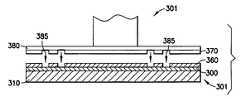
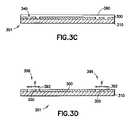
- FIGS. 3A-3Dthe formation of metal lines 392 isolated by a porous film 300 is discussed in detail.
- the embodiments described with reference to FIGS. 3A-3Edescribe the formation of particular circuit features (metal lines 392 ) isolated by the porous film 300 .
- additional circuit featuresmay be formed and isolated by the porous film 300 .
- FIG. 4is a flow chart summarizing embodiments of forming a metal lines 392 in a semiconductor wafer 301 as described in FIGS. 3A-3D . Therefore, FIG. 4 is referenced throughout remaining portions of the description as an aid in describing the embodiments referenced in FIGS. 3A-3D .
- a semiconductor wafer 301is shown having a porous film 300 formed on a substrate 310 thereof as indicated at 410 of FIG. 4 .
- the porous film 300is formed according to methods described above with reference to FIGS. 1 and 2 and includes a substantially uniform porosity and dielectric constant value throughout.
- a chemically resilient photo resist 360is placed above the porous film 300 .
- the photo resist 360is then patterned as indicted at 430 with a photomasking tool 301 as shown in FIG. 3A .
- the photo resist 360is subject to deterioration upon exposure to certain conditions such as ultraviolet (UV) light. Therefore, in order to pattern the photo resist 360 , the photomasking tool 301 includes UV emitting portions 385 defined and contained by a mask 370 . In this manner the photomasking tool 301 may be applied to pattern the photo resist 360 as shown in FIG. 3A .
- Conventional etching techniquesmay follow the patterning of the photo resist 360 . That is, as indicated at 440 of FIG. 4 ., conventional chemical etchants may be delivered to the semiconductor wafer 301 to form trenches 340 in the porous film 300 .
- the patterned photo resist 360protects the porous film 300 where present. However, the patterning described above, allows chemical etchants to reach the porous film 300 at certain locations where the trenches 340 are formed.
- the patterned photo resist 360may be removed as indicated at 450 of FIG. 4 . This may be achieved for example by further exposure to UV light, leaving the semiconductor wafer 301 as shown in FIG. 3B .
- the semiconductor wafer 301is metalized as indicated at 460 .
- copper, aluminum, or other electrically conductive materialmay be deposited above the substrate 310 and porous film 300 while filling the trenches 340 . This may be achieved by conventional techniques such as CVD described above.
- the resulting metal layer 390remains to be isolated and formed into independent circuit features as described below.
- the semiconductor wafer 301is shown following the application of conventional chemical mechanical polishing (CMP) to isolate circuit features in the form of metal lines 392 as indicated at 470 of FIG. 4 . That is, a chemical slurry is delivered, and a rotating polishing pad applied, to the semiconductor wafer 301 until the metal lines 392 are left isolated by the porous film 300 .
- CMPchemical mechanical polishing
- a first pair 398 of metal lines 392 at one location of the semiconductor wafer 301may be compared to a second pair 399 at another location.
- Each pair 398 , 399includes metal lines 392 separated by porous film 300 of a distance (d). While the pairs 398 , 399 are located in entirely different areas of the semiconductor wafer 301 , the porous film 300 , formed according to methods described herein, is of substantially uniform porosity throughout.
- the dielectric constant (k) valueremains substantially consistent. That is, the dielectric constant (k) value for the first pair 398 of metal lines 392 is substantially equivalent to the dielectric constant value (k) for the second pair 399 .
- capacitance (C)(which is k ⁇ A/d) is less variable even as the dielectric constant (k) is lowered by the addition of a porosity.
- Resulting circuit features, such as the metal lines 392 , isolated by the porous film 300therefore perform in a more reliable and predictable manner. Further processing may follow wherein the semiconductor wafer 301 is sawed into individual dice for integrated circuits with individual circuit features. Nevertheless consistent performance may be expected from semiconductor devices employing such integrated circuits.
- Embodiments of the inventioninclude a porous dielectric film having a substantially uniform level of porosity throughout. Although exemplary embodiments describe particular circuit features isolated by a porous film additional embodiments are possible. Many changes, modifications, and substitutions may be made without departing from the spirit and scope of these embodiments.
Landscapes
- Engineering & Computer Science (AREA)
- Chemical & Material Sciences (AREA)
- Chemical Kinetics & Catalysis (AREA)
- Physics & Mathematics (AREA)
- Condensed Matter Physics & Semiconductors (AREA)
- General Physics & Mathematics (AREA)
- Manufacturing & Machinery (AREA)
- Computer Hardware Design (AREA)
- Microelectronics & Electronic Packaging (AREA)
- Power Engineering (AREA)
- Internal Circuitry In Semiconductor Integrated Circuit Devices (AREA)
- Formation Of Insulating Films (AREA)
Abstract
Description
Claims (9)
Priority Applications (1)
| Application Number | Priority Date | Filing Date | Title |
|---|---|---|---|
| US11/071,621US7342295B2 (en) | 2002-11-21 | 2005-03-03 | Porogen material |
Applications Claiming Priority (2)
| Application Number | Priority Date | Filing Date | Title |
|---|---|---|---|
| US10/301,109US7456488B2 (en) | 2002-11-21 | 2002-11-21 | Porogen material |
| US11/071,621US7342295B2 (en) | 2002-11-21 | 2005-03-03 | Porogen material |
Related Parent Applications (1)
| Application Number | Title | Priority Date | Filing Date |
|---|---|---|---|
| US10/301,109DivisionUS7456488B2 (en) | 2001-12-13 | 2002-11-21 | Porogen material |
Publications (2)
| Publication Number | Publication Date |
|---|---|
| US20050161763A1 US20050161763A1 (en) | 2005-07-28 |
| US7342295B2true US7342295B2 (en) | 2008-03-11 |
Family
ID=32324473
Family Applications (2)
| Application Number | Title | Priority Date | Filing Date |
|---|---|---|---|
| US10/301,109Expired - Fee RelatedUS7456488B2 (en) | 2001-12-13 | 2002-11-21 | Porogen material |
| US11/071,621Expired - LifetimeUS7342295B2 (en) | 2002-11-21 | 2005-03-03 | Porogen material |
Family Applications Before (1)
| Application Number | Title | Priority Date | Filing Date |
|---|---|---|---|
| US10/301,109Expired - Fee RelatedUS7456488B2 (en) | 2001-12-13 | 2002-11-21 | Porogen material |
Country Status (3)
| Country | Link |
|---|---|
| US (2) | US7456488B2 (en) |
| AU (1) | AU2003294408A1 (en) |
| WO (1) | WO2004049398A2 (en) |
Cited By (2)
| Publication number | Priority date | Publication date | Assignee | Title |
|---|---|---|---|---|
| US20060235182A1 (en)* | 2001-12-13 | 2006-10-19 | Chongying Xu | Method for removal of impurities in cyclic siloxanes useful as precursors for low dielectric constant thin films |
| US20110204492A1 (en)* | 2010-02-23 | 2011-08-25 | Applied Materials, Inc. | Microelectronic structure including a low K dielectric and a method of controlling carbon distribution in the structure |
Families Citing this family (20)
| Publication number | Priority date | Publication date | Assignee | Title |
|---|---|---|---|---|
| US6800571B2 (en)* | 1998-09-29 | 2004-10-05 | Applied Materials Inc. | CVD plasma assisted low dielectric constant films |
| US6541367B1 (en)* | 2000-01-18 | 2003-04-01 | Applied Materials, Inc. | Very low dielectric constant plasma-enhanced CVD films |
| US7456488B2 (en)* | 2002-11-21 | 2008-11-25 | Advanced Technology Materials, Inc. | Porogen material |
| US8293001B2 (en)* | 2002-04-17 | 2012-10-23 | Air Products And Chemicals, Inc. | Porogens, porogenated precursors and methods for using the same to provide porous organosilica glass films with low dielectric constants |
| US8951342B2 (en) | 2002-04-17 | 2015-02-10 | Air Products And Chemicals, Inc. | Methods for using porogens for low k porous organosilica glass films |
| US6846515B2 (en)* | 2002-04-17 | 2005-01-25 | Air Products And Chemicals, Inc. | Methods for using porogens and/or porogenated precursors to provide porous organosilica glass films with low dielectric constants |
| US7384471B2 (en)* | 2002-04-17 | 2008-06-10 | Air Products And Chemicals, Inc. | Porogens, porogenated precursors and methods for using the same to provide porous organosilica glass films with low dielectric constants |
| US9061317B2 (en) | 2002-04-17 | 2015-06-23 | Air Products And Chemicals, Inc. | Porogens, porogenated precursors and methods for using the same to provide porous organosilica glass films with low dielectric constants |
| US20080268177A1 (en)* | 2002-05-17 | 2008-10-30 | Air Products And Chemicals, Inc. | Porogens, Porogenated Precursors and Methods for Using the Same to Provide Porous Organosilica Glass Films with Low Dielectric Constants |
| US6936551B2 (en)* | 2002-05-08 | 2005-08-30 | Applied Materials Inc. | Methods and apparatus for E-beam treatment used to fabricate integrated circuit devices |
| US6953698B2 (en)* | 2003-06-19 | 2005-10-11 | Agilent Technologies, Inc. | Methods for making microwave circuits |
| US7148263B2 (en)* | 2004-07-14 | 2006-12-12 | Honeywell International Inc. | Hybrid inorganic/organic low k dielectric films with improved mechanical strength |
| US7132374B2 (en)* | 2004-08-17 | 2006-11-07 | Cecilia Y. Mak | Method for depositing porous films |
| US7332445B2 (en)* | 2004-09-28 | 2008-02-19 | Air Products And Chemicals, Inc. | Porous low dielectric constant compositions and methods for making and using same |
| US7465652B2 (en) | 2005-08-16 | 2008-12-16 | Sony Corporation | Method of forming a catalyst layer on the barrier layer of a conductive interconnect of a semiconductor device |
| US7422975B2 (en) | 2005-08-18 | 2008-09-09 | Sony Corporation | Composite inter-level dielectric structure for an integrated circuit |
| US8586468B2 (en) | 2005-08-24 | 2013-11-19 | Sony Corporation | Integrated circuit chip stack employing carbon nanotube interconnects |
| US7251799B2 (en) | 2005-08-30 | 2007-07-31 | Sony Corporation | Metal interconnect structure for integrated circuits and a design rule therefor |
| US8053375B1 (en)* | 2006-11-03 | 2011-11-08 | Advanced Technology Materials, Inc. | Super-dry reagent compositions for formation of ultra low k films |
| EP3002262B1 (en) | 2014-10-01 | 2018-06-27 | Heraeus Quarzglas GmbH & Co. KG | Method for the manufacture of synthetic quartz glass with polymerizable polyalkylsiloxane |
Citations (54)
| Publication number | Priority date | Publication date | Assignee | Title |
|---|---|---|---|---|
| JPS50111198A (en) | 1974-01-28 | 1975-09-01 | ||
| US4087448A (en) | 1976-04-08 | 1978-05-02 | Th. Goldschmidt Ag | Process for preparing equilibrated organopolysiloxane mixtures with organosulfonic acid groups linked to silicon |
| US4127598A (en) | 1977-02-22 | 1978-11-28 | Mcentee Harry R | Process for removing biphenyls from chlorosilanes |
| US4156689A (en) | 1978-02-13 | 1979-05-29 | General Electric Company | Purification of hydrosilanes and siloxanes |
| US4374110A (en) | 1981-06-15 | 1983-02-15 | Motorola, Inc. | Purification of silicon source materials |
| US4670299A (en) | 1984-11-01 | 1987-06-02 | Fujitsu Limited | Preparation of lower alkyl polysilsesquioxane and formation of insulating layer of silylated polymer on electronic circuit board |
| US4745169A (en) | 1985-05-10 | 1988-05-17 | Hitachi, Ltd. | Alkali-soluble siloxane polymer, silmethylene polymer, and polyorganosilsesquioxane polymer |
| US4755370A (en) | 1982-03-18 | 1988-07-05 | General Electric Company | Purification of silicon halides |
| US4764631A (en) | 1988-01-15 | 1988-08-16 | Dow Corning Corporation | Preparation of cyclopolydiorganosiloxanes via vapor phase rearrangement |
| US4871616A (en) | 1986-10-20 | 1989-10-03 | Toshiba Silicone Co., Ltd. | Surface-treated poly methyl silsequoxane powder |
| US5043789A (en) | 1990-03-15 | 1991-08-27 | International Business Machines Corporation | Planarizing silsesquioxane copolymer coating |
| US5047492A (en) | 1988-11-03 | 1991-09-10 | Wacker-Chemie Gmbh | Organooligosilsesquioxanes |
| US5098865A (en) | 1989-11-02 | 1992-03-24 | Machado Jose R | High step coverage silicon oxide thin films |
| US5204314A (en) | 1990-07-06 | 1993-04-20 | Advanced Technology Materials, Inc. | Method for delivering an involatile reagent in vapor form to a CVD reactor |
| US5210250A (en) | 1991-08-28 | 1993-05-11 | Shin-Etsu Chemical Co. Ltd. | Method for decolorizing purification of halogenated silane |
| EP0543665A1 (en) | 1991-11-22 | 1993-05-26 | Shin-Etsu Chemical Co., Ltd. | Siloxane purification |
| US5276173A (en) | 1992-10-05 | 1994-01-04 | Dow Corning Corporation | Method for removal for ionic chloride from hydroxyl-terminated siloxanes |
| US5281686A (en) | 1991-05-24 | 1994-01-25 | General Electric Company | Method for making silicone-polyphenylene ether graft copolymers and products |
| US5312947A (en) | 1992-09-24 | 1994-05-17 | Shin-Etsu Chemical Co., Ltd. | Siloxane purification |
| US5484867A (en) | 1993-08-12 | 1996-01-16 | The University Of Dayton | Process for preparation of polyhedral oligomeric silsesquioxanes and systhesis of polymers containing polyhedral oligomeric silsesqioxane group segments |
| US5536323A (en) | 1990-07-06 | 1996-07-16 | Advanced Technology Materials, Inc. | Apparatus for flash vaporization delivery of reagents |
| US5711816A (en) | 1990-07-06 | 1998-01-27 | Advanced Technolgy Materials, Inc. | Source reagent liquid delivery apparatus, and chemical vapor deposition system comprising same |
| WO1998015499A1 (en) | 1996-10-08 | 1998-04-16 | Corning Incorporated | Method of inhibiting gelling of siloxane feedstocks and a gel inhibited feedstock |
| US5804040A (en) | 1995-09-08 | 1998-09-08 | Kaneka Corporation | Purification process for silane compound |
| US5879649A (en) | 1995-12-19 | 1999-03-09 | Corning Incorporated | Method for purifying polyalkylsiloxanes and the resulting products |
| US6114500A (en) | 1998-01-08 | 2000-09-05 | Shin-Etsu Chemical Co., Ltd. | Purification of organic silicon polymer |
| US6147009A (en) | 1998-06-29 | 2000-11-14 | International Business Machines Corporation | Hydrogenated oxidized silicon carbon material |
| US6171945B1 (en) | 1998-10-22 | 2001-01-09 | Applied Materials, Inc. | CVD nanoporous silica low dielectric constant films |
| US6331494B1 (en) | 1999-12-30 | 2001-12-18 | Novellus Systems, Inc. | Deposition of low dielectric constant thin film without use of an oxidizer |
| US6368359B1 (en) | 1999-12-17 | 2002-04-09 | General Electric Company | Process for stabilization of dry cleaning solutions |
| US6383955B1 (en) | 1998-02-05 | 2002-05-07 | Asm Japan K.K. | Silicone polymer insulation film on semiconductor substrate and method for forming the film |
| US6420441B1 (en) | 1999-10-01 | 2002-07-16 | Shipley Company, L.L.C. | Porous materials |
| US6451712B1 (en)* | 2000-12-18 | 2002-09-17 | International Business Machines Corporation | Method for forming a porous dielectric material layer in a semiconductor device and device formed |
| US20020142579A1 (en) | 2001-01-17 | 2002-10-03 | Vincent Jean Louise | Organosilicon precursors for interlayer dielectric films with low dielectric constants |
| US6486082B1 (en) | 2001-06-18 | 2002-11-26 | Applied Materials, Inc. | CVD plasma assisted lower dielectric constant sicoh film |
| US6495479B1 (en)* | 2000-05-05 | 2002-12-17 | Honeywell International, Inc. | Simplified method to produce nanoporous silicon-based films |
| US6528409B1 (en) | 2002-04-29 | 2003-03-04 | Advanced Micro Devices, Inc. | Interconnect structure formed in porous dielectric material with minimized degradation and electromigration |
| US20030044531A1 (en)* | 2001-09-04 | 2003-03-06 | Hiroshi Ishida | Film forming apparatus and film forming method |
| EP1321469A1 (en) | 2001-12-21 | 2003-06-25 | Air Products And Chemicals, Inc. | Stabilizers to inhibit the polymerization of substituted cyclotetrasiloxane |
| US20030124785A1 (en)* | 2001-12-31 | 2003-07-03 | Chongying Xu | Supercritical fluid-assisted deposition of materials on semiconductor substrates |
| US20030146451A1 (en)* | 2001-03-14 | 2003-08-07 | Huang Elbert Emin | Nitrogen-containing polymers as porogens in the preparation of highly porous, low dielectric constant materials |
| US6632531B2 (en) | 2001-02-15 | 2003-10-14 | Rohm And Haas Company | Porous particles, their aqueous dispersions, and method of preparation |
| US20030232137A1 (en) | 2002-04-17 | 2003-12-18 | Vrtis Raymond Nicholas | Porogens, porogenated precursors and methods for using the same to provide porous organosilica glass films with low dielectric constants |
| US20040039219A1 (en) | 2001-12-13 | 2004-02-26 | Tianniu Chen | Stabilized cyclosiloxanes for use as CVD precursors for low-dielectric constant thin films |
| WO2004027110A2 (en) | 2002-09-18 | 2004-04-01 | Arch Specialty Chemicals, Inc. | Additives to prevent degradation of alkyl-hydrogen siloxanes |
| US20040071878A1 (en)* | 2002-08-15 | 2004-04-15 | Interuniversitair Microelektronica Centrum (Imec Vzw) | Surface preparation using plasma for ALD Films |
| US20040087184A1 (en)* | 2000-04-04 | 2004-05-06 | Applied Materials Inc., A Delaware Corporation | Ionic additives for extreme low dielectric constant chemical formulations |
| US20040102006A1 (en) | 2002-11-21 | 2004-05-27 | Chongying Xu | Porogen material |
| US20040137243A1 (en) | 2002-10-21 | 2004-07-15 | Massachusetts Institute Of Technology | Chemical vapor deposition of organosilicate thin films |
| US20050130404A1 (en)* | 2002-05-08 | 2005-06-16 | Applied Materials, Inc. | Methods and apparatus for e-beam treatment used to fabricate integrated circuit devices |
| US7056560B2 (en) | 2002-05-08 | 2006-06-06 | Applies Materials Inc. | Ultra low dielectric materials based on hybrid system of linear silicon precursor and organic porogen by plasma-enhanced chemical vapor deposition (PECVD) |
| US7060330B2 (en) | 2002-05-08 | 2006-06-13 | Applied Materials, Inc. | Method for forming ultra low k films using electron beam |
| US7101948B2 (en) | 2001-12-21 | 2006-09-05 | Air Products And Chemicals, Inc. | Stabilizers to inhibit the polymerization of substituted cyclotetrasiloxane |
| US7108771B2 (en) | 2001-12-13 | 2006-09-19 | Advanced Technology Materials, Inc. | Method for removal of impurities in cyclic siloxanes useful as precursors for low dielectric constant thin films |
Family Cites Families (5)
| Publication number | Priority date | Publication date | Assignee | Title |
|---|---|---|---|---|
| US4347110A (en)* | 1980-07-10 | 1982-08-31 | Scm Corporation | Method for tall oil recovery and apparatus therefor |
| US6366359B1 (en)* | 1998-04-09 | 2002-04-02 | Canon Kabushiki Kaisha | Integrated digital television and video printer |
| US6582673B1 (en)* | 2000-03-17 | 2003-06-24 | University Of Central Florida | Carbon nanotube with a graphitic outer layer: process and application |
| US6656837B2 (en)* | 2001-10-11 | 2003-12-02 | Applied Materials, Inc. | Method of eliminating photoresist poisoning in damascene applications |
| US6846515B2 (en)* | 2002-04-17 | 2005-01-25 | Air Products And Chemicals, Inc. | Methods for using porogens and/or porogenated precursors to provide porous organosilica glass films with low dielectric constants |
- 2002
- 2002-11-21USUS10/301,109patent/US7456488B2/ennot_activeExpired - Fee Related
- 2003
- 2003-11-19AUAU2003294408Apatent/AU2003294408A1/ennot_activeAbandoned
- 2003-11-19WOPCT/US2003/037171patent/WO2004049398A2/ennot_activeApplication Discontinuation
- 2005
- 2005-03-03USUS11/071,621patent/US7342295B2/ennot_activeExpired - Lifetime
Patent Citations (63)
| Publication number | Priority date | Publication date | Assignee | Title |
|---|---|---|---|---|
| JPS50111198A (en) | 1974-01-28 | 1975-09-01 | ||
| US4087448A (en) | 1976-04-08 | 1978-05-02 | Th. Goldschmidt Ag | Process for preparing equilibrated organopolysiloxane mixtures with organosulfonic acid groups linked to silicon |
| US4127598A (en) | 1977-02-22 | 1978-11-28 | Mcentee Harry R | Process for removing biphenyls from chlorosilanes |
| US4127598B1 (en) | 1977-02-22 | 1985-09-10 | ||
| US4156689A (en) | 1978-02-13 | 1979-05-29 | General Electric Company | Purification of hydrosilanes and siloxanes |
| US4374110A (en) | 1981-06-15 | 1983-02-15 | Motorola, Inc. | Purification of silicon source materials |
| US4755370A (en) | 1982-03-18 | 1988-07-05 | General Electric Company | Purification of silicon halides |
| US4670299A (en) | 1984-11-01 | 1987-06-02 | Fujitsu Limited | Preparation of lower alkyl polysilsesquioxane and formation of insulating layer of silylated polymer on electronic circuit board |
| US4745169A (en) | 1985-05-10 | 1988-05-17 | Hitachi, Ltd. | Alkali-soluble siloxane polymer, silmethylene polymer, and polyorganosilsesquioxane polymer |
| US4871616A (en) | 1986-10-20 | 1989-10-03 | Toshiba Silicone Co., Ltd. | Surface-treated poly methyl silsequoxane powder |
| US4764631A (en) | 1988-01-15 | 1988-08-16 | Dow Corning Corporation | Preparation of cyclopolydiorganosiloxanes via vapor phase rearrangement |
| US5047492A (en) | 1988-11-03 | 1991-09-10 | Wacker-Chemie Gmbh | Organooligosilsesquioxanes |
| US5098865A (en) | 1989-11-02 | 1992-03-24 | Machado Jose R | High step coverage silicon oxide thin films |
| US5043789A (en) | 1990-03-15 | 1991-08-27 | International Business Machines Corporation | Planarizing silsesquioxane copolymer coating |
| US5536323A (en) | 1990-07-06 | 1996-07-16 | Advanced Technology Materials, Inc. | Apparatus for flash vaporization delivery of reagents |
| US5204314A (en) | 1990-07-06 | 1993-04-20 | Advanced Technology Materials, Inc. | Method for delivering an involatile reagent in vapor form to a CVD reactor |
| US5711816A (en) | 1990-07-06 | 1998-01-27 | Advanced Technolgy Materials, Inc. | Source reagent liquid delivery apparatus, and chemical vapor deposition system comprising same |
| US5281686A (en) | 1991-05-24 | 1994-01-25 | General Electric Company | Method for making silicone-polyphenylene ether graft copolymers and products |
| US5210250A (en) | 1991-08-28 | 1993-05-11 | Shin-Etsu Chemical Co. Ltd. | Method for decolorizing purification of halogenated silane |
| EP0543665A1 (en) | 1991-11-22 | 1993-05-26 | Shin-Etsu Chemical Co., Ltd. | Siloxane purification |
| US5312947A (en) | 1992-09-24 | 1994-05-17 | Shin-Etsu Chemical Co., Ltd. | Siloxane purification |
| US5276173A (en) | 1992-10-05 | 1994-01-04 | Dow Corning Corporation | Method for removal for ionic chloride from hydroxyl-terminated siloxanes |
| US5484867A (en) | 1993-08-12 | 1996-01-16 | The University Of Dayton | Process for preparation of polyhedral oligomeric silsesquioxanes and systhesis of polymers containing polyhedral oligomeric silsesqioxane group segments |
| US5804040A (en) | 1995-09-08 | 1998-09-08 | Kaneka Corporation | Purification process for silane compound |
| US5879649A (en) | 1995-12-19 | 1999-03-09 | Corning Incorporated | Method for purifying polyalkylsiloxanes and the resulting products |
| WO1998015499A1 (en) | 1996-10-08 | 1998-04-16 | Corning Incorporated | Method of inhibiting gelling of siloxane feedstocks and a gel inhibited feedstock |
| US6114500A (en) | 1998-01-08 | 2000-09-05 | Shin-Etsu Chemical Co., Ltd. | Purification of organic silicon polymer |
| US6410463B1 (en) | 1998-02-05 | 2002-06-25 | Asm Japan K.K. | Method for forming film with low dielectric constant on semiconductor substrate |
| US6383955B1 (en) | 1998-02-05 | 2002-05-07 | Asm Japan K.K. | Silicone polymer insulation film on semiconductor substrate and method for forming the film |
| US6147009A (en) | 1998-06-29 | 2000-11-14 | International Business Machines Corporation | Hydrogenated oxidized silicon carbon material |
| US6171945B1 (en) | 1998-10-22 | 2001-01-09 | Applied Materials, Inc. | CVD nanoporous silica low dielectric constant films |
| US6420441B1 (en) | 1999-10-01 | 2002-07-16 | Shipley Company, L.L.C. | Porous materials |
| US6368359B1 (en) | 1999-12-17 | 2002-04-09 | General Electric Company | Process for stabilization of dry cleaning solutions |
| US6331494B1 (en) | 1999-12-30 | 2001-12-18 | Novellus Systems, Inc. | Deposition of low dielectric constant thin film without use of an oxidizer |
| US20040087184A1 (en)* | 2000-04-04 | 2004-05-06 | Applied Materials Inc., A Delaware Corporation | Ionic additives for extreme low dielectric constant chemical formulations |
| US6495479B1 (en)* | 2000-05-05 | 2002-12-17 | Honeywell International, Inc. | Simplified method to produce nanoporous silicon-based films |
| US20030077918A1 (en)* | 2000-05-05 | 2003-04-24 | Hui-Jung Wu | Simplified method to produce nanoporous silicon-based films |
| US6451712B1 (en)* | 2000-12-18 | 2002-09-17 | International Business Machines Corporation | Method for forming a porous dielectric material layer in a semiconductor device and device formed |
| US20020142579A1 (en) | 2001-01-17 | 2002-10-03 | Vincent Jean Louise | Organosilicon precursors for interlayer dielectric films with low dielectric constants |
| US6632531B2 (en) | 2001-02-15 | 2003-10-14 | Rohm And Haas Company | Porous particles, their aqueous dispersions, and method of preparation |
| US6670285B2 (en) | 2001-03-14 | 2003-12-30 | International Business Machines Corporation | Nitrogen-containing polymers as porogens in the preparation of highly porous, low dielectric constant materials |
| US20030146451A1 (en)* | 2001-03-14 | 2003-08-07 | Huang Elbert Emin | Nitrogen-containing polymers as porogens in the preparation of highly porous, low dielectric constant materials |
| US6486082B1 (en) | 2001-06-18 | 2002-11-26 | Applied Materials, Inc. | CVD plasma assisted lower dielectric constant sicoh film |
| US20050268849A1 (en)* | 2001-09-04 | 2005-12-08 | Tokyo Electron Limited | Film forming apparatus and film forming method |
| US20030044531A1 (en)* | 2001-09-04 | 2003-03-06 | Hiroshi Ishida | Film forming apparatus and film forming method |
| US7011864B2 (en)* | 2001-09-04 | 2006-03-14 | Tokyo Electron Limited | Film forming apparatus and film forming method |
| US20040039219A1 (en) | 2001-12-13 | 2004-02-26 | Tianniu Chen | Stabilized cyclosiloxanes for use as CVD precursors for low-dielectric constant thin films |
| US7108771B2 (en) | 2001-12-13 | 2006-09-19 | Advanced Technology Materials, Inc. | Method for removal of impurities in cyclic siloxanes useful as precursors for low dielectric constant thin films |
| US7101948B2 (en) | 2001-12-21 | 2006-09-05 | Air Products And Chemicals, Inc. | Stabilizers to inhibit the polymerization of substituted cyclotetrasiloxane |
| US6858697B2 (en) | 2001-12-21 | 2005-02-22 | Air Products And Chemicals, Inc. | Stabilizers to inhibit the polymerization of substituted cyclotetrasiloxane |
| EP1321469A1 (en) | 2001-12-21 | 2003-06-25 | Air Products And Chemicals, Inc. | Stabilizers to inhibit the polymerization of substituted cyclotetrasiloxane |
| US20050181613A1 (en)* | 2001-12-31 | 2005-08-18 | Chongying Xu | Supercritical fluid-assisted deposition of materials on semiconductor substrates |
| US20030124785A1 (en)* | 2001-12-31 | 2003-07-03 | Chongying Xu | Supercritical fluid-assisted deposition of materials on semiconductor substrates |
| US20030232137A1 (en) | 2002-04-17 | 2003-12-18 | Vrtis Raymond Nicholas | Porogens, porogenated precursors and methods for using the same to provide porous organosilica glass films with low dielectric constants |
| US6528409B1 (en) | 2002-04-29 | 2003-03-04 | Advanced Micro Devices, Inc. | Interconnect structure formed in porous dielectric material with minimized degradation and electromigration |
| US7056560B2 (en) | 2002-05-08 | 2006-06-06 | Applies Materials Inc. | Ultra low dielectric materials based on hybrid system of linear silicon precursor and organic porogen by plasma-enhanced chemical vapor deposition (PECVD) |
| US6936551B2 (en)* | 2002-05-08 | 2005-08-30 | Applied Materials Inc. | Methods and apparatus for E-beam treatment used to fabricate integrated circuit devices |
| US20050130404A1 (en)* | 2002-05-08 | 2005-06-16 | Applied Materials, Inc. | Methods and apparatus for e-beam treatment used to fabricate integrated circuit devices |
| US7060330B2 (en) | 2002-05-08 | 2006-06-13 | Applied Materials, Inc. | Method for forming ultra low k films using electron beam |
| US20040071878A1 (en)* | 2002-08-15 | 2004-04-15 | Interuniversitair Microelektronica Centrum (Imec Vzw) | Surface preparation using plasma for ALD Films |
| WO2004027110A2 (en) | 2002-09-18 | 2004-04-01 | Arch Specialty Chemicals, Inc. | Additives to prevent degradation of alkyl-hydrogen siloxanes |
| US20040137243A1 (en) | 2002-10-21 | 2004-07-15 | Massachusetts Institute Of Technology | Chemical vapor deposition of organosilicate thin films |
| US20040102006A1 (en) | 2002-11-21 | 2004-05-27 | Chongying Xu | Porogen material |
Non-Patent Citations (5)
| Title |
|---|
| A. Grill, et al., "Ultralow-k dielectrics prepared by plasm-enhanced chemical vapor deposition" Applied Physics Letters, vol. 79, No. 6, pp. 803-805, date is not available. |
| Grill, Alfred, et al., Novel low-k dual-phase materials pepared by PECVD, Mat. Res. Soc. Symp. Proc., 2000, vol. 612. |
| Laxman, Ravi K., et al., Synthesizing Low-K CVD Materials for Fab Use. Semiconductor International, Nov. 1, 2000. |
| Mantz, R.A., et al., Thermolysis of Polyhedral Oligomeric Silsesquioxane (POSS) Macromers and POSS-Siloxane Copolymers, Chem. Mater., Jun. 1996, pp. 1250-1259, vol. 8, No. 6. |
| Wang, Albert, et al., TMCTS for gate dielectric in thin films transistors, Mat Res. Soc. Meeting, 1996. |
Cited By (3)
| Publication number | Priority date | Publication date | Assignee | Title |
|---|---|---|---|---|
| US20060235182A1 (en)* | 2001-12-13 | 2006-10-19 | Chongying Xu | Method for removal of impurities in cyclic siloxanes useful as precursors for low dielectric constant thin films |
| US20110204492A1 (en)* | 2010-02-23 | 2011-08-25 | Applied Materials, Inc. | Microelectronic structure including a low K dielectric and a method of controlling carbon distribution in the structure |
| US8349746B2 (en) | 2010-02-23 | 2013-01-08 | Applied Materials, Inc. | Microelectronic structure including a low k dielectric and a method of controlling carbon distribution in the structure |
Also Published As
| Publication number | Publication date |
|---|---|
| AU2003294408A1 (en) | 2004-06-18 |
| WO2004049398B1 (en) | 2005-07-14 |
| WO2004049398A2 (en) | 2004-06-10 |
| US7456488B2 (en) | 2008-11-25 |
| AU2003294408A8 (en) | 2004-06-18 |
| WO2004049398A3 (en) | 2005-06-09 |
| US20040102006A1 (en) | 2004-05-27 |
| US20050161763A1 (en) | 2005-07-28 |
Similar Documents
| Publication | Publication Date | Title |
|---|---|---|
| US7342295B2 (en) | Porogen material | |
| JP3276963B2 (en) | Method of forming dielectric film on substrate | |
| JP5271255B2 (en) | Method for removing damaged dielectric material | |
| KR100447684B1 (en) | Organosilicon precursors for interlayer dielectric films with low dielectric constants | |
| KR100696035B1 (en) | CDN nanoporous silica low dielectric constant membrane | |
| TWI613724B (en) | Method for forming sioch film using organoaminosilane annealing | |
| KR100661201B1 (en) | Processes for depositing and etching dielectric layers | |
| JP5380797B2 (en) | Manufacturing method of semiconductor device | |
| US7723237B2 (en) | Method for selective removal of damaged multi-stack bilayer films | |
| JP2004006983A (en) | Low κ dielectric inorganic / organic hybrid film | |
| JP2004507108A (en) | Low dielectric constant silicon nitride film and method for forming the same, semiconductor device and apparatus for manufacturing the same | |
| US7830012B2 (en) | Material for forming exposure light-blocking film, multilayer interconnection structure and manufacturing method thereof, and semiconductor device | |
| US7985700B2 (en) | Composition for forming insulating film and method for fabricating semiconductor device | |
| US7034380B2 (en) | Low-dielectric constant structure with a multilayer stack of thin films with pores | |
| KR102642184B1 (en) | Semiconductor device manufacturing method | |
| KR20050102620A (en) | Patterning layers comprised of spin-on ceramic films | |
| JP5470687B2 (en) | Silicon compound, ultraviolet absorber, multilayer wiring device manufacturing method, and multilayer wiring device | |
| KR101443999B1 (en) | Method for manufacturing semiconductor device | |
| KR20050084286A (en) | Nitrogen-free dielectric anti-reflective coating and hardmask |
Legal Events
| Date | Code | Title | Description |
|---|---|---|---|
| STCF | Information on status: patent grant | Free format text:PATENTED CASE | |
| FEPP | Fee payment procedure | Free format text:PAYOR NUMBER ASSIGNED (ORIGINAL EVENT CODE: ASPN); ENTITY STATUS OF PATENT OWNER: LARGE ENTITY | |
| CC | Certificate of correction | ||
| FPAY | Fee payment | Year of fee payment:4 | |
| AS | Assignment | Owner name:GOLDMAN SACHS BANK USA, AS COLLATERAL AGENT, NEW YORK Free format text:SECURITY INTEREST;ASSIGNORS:ENTEGRIS, INC.;POCO GRAPHITE, INC.;ATMI, INC.;AND OTHERS;REEL/FRAME:032815/0852 Effective date:20140430 Owner name:GOLDMAN SACHS BANK USA, AS COLLATERAL AGENT, NEW Y Free format text:SECURITY INTEREST;ASSIGNORS:ENTEGRIS, INC.;POCO GRAPHITE, INC.;ATMI, INC.;AND OTHERS;REEL/FRAME:032815/0852 Effective date:20140430 | |
| AS | Assignment | Owner name:GOLDMAN SACHS BANK USA, AS COLLATERAL AGENT, NEW YORK Free format text:SECURITY INTEREST;ASSIGNORS:ENTEGRIS, INC.;POCO GRAPHITE, INC.;ATMI, INC.;AND OTHERS;REEL/FRAME:032812/0192 Effective date:20140430 Owner name:GOLDMAN SACHS BANK USA, AS COLLATERAL AGENT, NEW Y Free format text:SECURITY INTEREST;ASSIGNORS:ENTEGRIS, INC.;POCO GRAPHITE, INC.;ATMI, INC.;AND OTHERS;REEL/FRAME:032812/0192 Effective date:20140430 | |
| AS | Assignment | Owner name:ENTEGRIS, INC., MASSACHUSETTS Free format text:ASSIGNMENT OF ASSIGNORS INTEREST;ASSIGNOR:ADVANCED TECHNOLOGY MATERIALS, INC.;REEL/FRAME:034894/0025 Effective date:20150204 | |
| FPAY | Fee payment | Year of fee payment:8 | |
| AS | Assignment | Owner name:ENTEGRIS, INC., MASSACHUSETTS Free format text:RELEASE BY SECURED PARTY;ASSIGNOR:GOLDMAN SACHS BANK USA, AS COLLATERAL AGENT;REEL/FRAME:047477/0032 Effective date:20181106 Owner name:ADVANCED TECHNOLOGY MATERIALS, INC., CONNECTICUT Free format text:RELEASE BY SECURED PARTY;ASSIGNOR:GOLDMAN SACHS BANK USA, AS COLLATERAL AGENT;REEL/FRAME:047477/0032 Effective date:20181106 Owner name:ATMI PACKAGING, INC., CONNECTICUT Free format text:RELEASE BY SECURED PARTY;ASSIGNOR:GOLDMAN SACHS BANK USA, AS COLLATERAL AGENT;REEL/FRAME:047477/0032 Effective date:20181106 Owner name:ATMI, INC., CONNECTICUT Free format text:RELEASE BY SECURED PARTY;ASSIGNOR:GOLDMAN SACHS BANK USA, AS COLLATERAL AGENT;REEL/FRAME:047477/0032 Effective date:20181106 Owner name:POCO GRAPHITE, INC., MASSACHUSETTS Free format text:RELEASE BY SECURED PARTY;ASSIGNOR:GOLDMAN SACHS BANK USA, AS COLLATERAL AGENT;REEL/FRAME:047477/0032 Effective date:20181106 Owner name:POCO GRAPHITE, INC., MASSACHUSETTS Free format text:RELEASE BY SECURED PARTY;ASSIGNOR:GOLDMAN SACHS BANK USA, AS COLLATERAL AGENT;REEL/FRAME:047477/0151 Effective date:20181106 Owner name:ATMI, INC., CONNECTICUT Free format text:RELEASE BY SECURED PARTY;ASSIGNOR:GOLDMAN SACHS BANK USA, AS COLLATERAL AGENT;REEL/FRAME:047477/0151 Effective date:20181106 Owner name:ENTEGRIS, INC., MASSACHUSETTS Free format text:RELEASE BY SECURED PARTY;ASSIGNOR:GOLDMAN SACHS BANK USA, AS COLLATERAL AGENT;REEL/FRAME:047477/0151 Effective date:20181106 Owner name:ATMI PACKAGING, INC., CONNECTICUT Free format text:RELEASE BY SECURED PARTY;ASSIGNOR:GOLDMAN SACHS BANK USA, AS COLLATERAL AGENT;REEL/FRAME:047477/0151 Effective date:20181106 Owner name:ADVANCED TECHNOLOGY MATERIALS, INC., CONNECTICUT Free format text:RELEASE BY SECURED PARTY;ASSIGNOR:GOLDMAN SACHS BANK USA, AS COLLATERAL AGENT;REEL/FRAME:047477/0151 Effective date:20181106 | |
| AS | Assignment | Owner name:GOLDMAN SACHS BANK USA, NEW YORK Free format text:SECURITY INTEREST;ASSIGNORS:ENTEGRIS, INC.;SAES PURE GAS, INC.;REEL/FRAME:048811/0679 Effective date:20181106 | |
| MAFP | Maintenance fee payment | Free format text:PAYMENT OF MAINTENANCE FEE, 12TH YEAR, LARGE ENTITY (ORIGINAL EVENT CODE: M1553); ENTITY STATUS OF PATENT OWNER: LARGE ENTITY Year of fee payment:12 | |
| AS | Assignment | Owner name:MORGAN STANLEY SENIOR FUNDING, INC., MARYLAND Free format text:ASSIGNMENT OF PATENT SECURITY INTEREST RECORDED AT REEL/FRAME 048811/0679;ASSIGNOR:GOLDMAN SACHS BANK USA;REEL/FRAME:050965/0035 Effective date:20191031 | |
| AS | Assignment | Owner name:TRUIST BANK, AS NOTES COLLATERAL AGENT, NORTH CAROLINA Free format text:SECURITY INTEREST;ASSIGNORS:ENTEGRIS, INC.;ENTEGRIS GP, INC.;POCO GRAPHITE, INC.;AND OTHERS;REEL/FRAME:060613/0072 Effective date:20220706 |