US7341956B1 - Disposable hard mask for forming bit lines - Google Patents
Disposable hard mask for forming bit linesDownload PDFInfo
- Publication number
- US7341956B1 US7341956B1US11/100,563US10056305AUS7341956B1US 7341956 B1US7341956 B1US 7341956B1US 10056305 AUS10056305 AUS 10056305AUS 7341956 B1US7341956 B1US 7341956B1
- Authority
- US
- United States
- Prior art keywords
- hard mask
- forming
- mask structures
- layer
- structures
- Prior art date
- Legal status (The legal status is an assumption and is not a legal conclusion. Google has not performed a legal analysis and makes no representation as to the accuracy of the status listed.)
- Active, expires
Links
- 238000000034methodMethods0.000claimsabstractdescription41
- 239000004065semiconductorSubstances0.000claimsabstractdescription30
- 239000000463materialSubstances0.000claimsdescription18
- 229920002120photoresistant polymerPolymers0.000claimsdescription16
- 238000005530etchingMethods0.000claimsdescription7
- 239000007943implantSubstances0.000claimsdescription6
- 239000006117anti-reflective coatingSubstances0.000claimsdescription4
- 238000005468ion implantationMethods0.000claimsdescription4
- 238000000059patterningMethods0.000claimsdescription3
- 229920000642polymerPolymers0.000claimsdescription2
- 239000003575carbonaceous materialSubstances0.000claims1
- 239000010410layerSubstances0.000description49
- 238000003860storageMethods0.000description10
- VYPSYNLAJGMNEJ-UHFFFAOYSA-NSilicium dioxideChemical compoundO=[Si]=OVYPSYNLAJGMNEJ-UHFFFAOYSA-N0.000description6
- 239000002019doping agentSubstances0.000description6
- 238000004519manufacturing processMethods0.000description5
- 230000015572biosynthetic processEffects0.000description4
- 239000011295pitchSubstances0.000description4
- 229910052814silicon oxideInorganic materials0.000description3
- RYGMFSIKBFXOCR-UHFFFAOYSA-NCopperChemical compound[Cu]RYGMFSIKBFXOCR-UHFFFAOYSA-N0.000description2
- 229910052581Si3N4Inorganic materials0.000description2
- 229910052782aluminiumInorganic materials0.000description2
- XAGFODPZIPBFFR-UHFFFAOYSA-NaluminiumChemical compound[Al]XAGFODPZIPBFFR-UHFFFAOYSA-N0.000description2
- 238000005229chemical vapour depositionMethods0.000description2
- 229910052802copperInorganic materials0.000description2
- 239000010949copperSubstances0.000description2
- 239000003989dielectric materialSubstances0.000description2
- 230000006870functionEffects0.000description2
- 238000002513implantationMethods0.000description2
- 229910052751metalInorganic materials0.000description2
- 239000002184metalSubstances0.000description2
- 239000005360phosphosilicate glassSubstances0.000description2
- 229910021420polycrystalline siliconInorganic materials0.000description2
- 229920005591polysiliconPolymers0.000description2
- 229910052710siliconInorganic materials0.000description2
- 239000010703siliconSubstances0.000description2
- 239000000377silicon dioxideSubstances0.000description2
- HQVNEWCFYHHQES-UHFFFAOYSA-Nsilicon nitrideChemical compoundN12[Si]34N5[Si]62N3[Si]51N64HQVNEWCFYHHQES-UHFFFAOYSA-N0.000description2
- 239000000758substrateSubstances0.000description2
- ZOXJGFHDIHLPTG-UHFFFAOYSA-NBoronChemical compound[B]ZOXJGFHDIHLPTG-UHFFFAOYSA-N0.000description1
- OKTJSMMVPCPJKN-UHFFFAOYSA-NCarbonChemical compound[C]OKTJSMMVPCPJKN-UHFFFAOYSA-N0.000description1
- 229910000577Silicon-germaniumInorganic materials0.000description1
- LEVVHYCKPQWKOP-UHFFFAOYSA-N[Si].[Ge]Chemical compound[Si].[Ge]LEVVHYCKPQWKOP-UHFFFAOYSA-N0.000description1
- 229910003481amorphous carbonInorganic materials0.000description1
- 229910052785arsenicInorganic materials0.000description1
- RQNWIZPPADIBDY-UHFFFAOYSA-Narsenic atomChemical compound[As]RQNWIZPPADIBDY-UHFFFAOYSA-N0.000description1
- 229910052796boronInorganic materials0.000description1
- 229910052799carbonInorganic materials0.000description1
- 229910052681coesiteInorganic materials0.000description1
- 229910052906cristobaliteInorganic materials0.000description1
- 230000001419dependent effectEffects0.000description1
- 238000000151depositionMethods0.000description1
- 230000008021depositionEffects0.000description1
- 229910052732germaniumInorganic materials0.000description1
- GNPVGFCGXDBREM-UHFFFAOYSA-Ngermanium atomChemical compound[Ge]GNPVGFCGXDBREM-UHFFFAOYSA-N0.000description1
- 239000002784hot electronSubstances0.000description1
- BHEPBYXIRTUNPN-UHFFFAOYSA-Nhydridophosphorus(.) (triplet)Chemical compound[PH]BHEPBYXIRTUNPN-UHFFFAOYSA-N0.000description1
- 238000002347injectionMethods0.000description1
- 239000007924injectionSubstances0.000description1
- 239000011229interlayerSubstances0.000description1
- 150000002500ionsChemical class0.000description1
- 238000012986modificationMethods0.000description1
- 230000004048modificationEffects0.000description1
- 239000012811non-conductive materialSubstances0.000description1
- 230000000149penetrating effectEffects0.000description1
- 238000005498polishingMethods0.000description1
- 235000012239silicon dioxideNutrition0.000description1
- 229910052682stishoviteInorganic materials0.000description1
- -1structuresSubstances0.000description1
- 239000000126substanceSubstances0.000description1
- 229910052905tridymiteInorganic materials0.000description1
Images


Classifications
- H—ELECTRICITY
- H10—SEMICONDUCTOR DEVICES; ELECTRIC SOLID-STATE DEVICES NOT OTHERWISE PROVIDED FOR
- H10B—ELECTRONIC MEMORY DEVICES
- H10B43/00—EEPROM devices comprising charge-trapping gate insulators
- H10B43/30—EEPROM devices comprising charge-trapping gate insulators characterised by the memory core region
- H—ELECTRICITY
- H01—ELECTRIC ELEMENTS
- H01L—SEMICONDUCTOR DEVICES NOT COVERED BY CLASS H10
- H01L21/00—Processes or apparatus adapted for the manufacture or treatment of semiconductor or solid state devices or of parts thereof
- H01L21/02—Manufacture or treatment of semiconductor devices or of parts thereof
- H01L21/04—Manufacture or treatment of semiconductor devices or of parts thereof the devices having potential barriers, e.g. a PN junction, depletion layer or carrier concentration layer
- H01L21/18—Manufacture or treatment of semiconductor devices or of parts thereof the devices having potential barriers, e.g. a PN junction, depletion layer or carrier concentration layer the devices having semiconductor bodies comprising elements of Group IV of the Periodic Table or AIIIBV compounds with or without impurities, e.g. doping materials
- H01L21/26—Bombardment with radiation
- H01L21/263—Bombardment with radiation with high-energy radiation
- H01L21/265—Bombardment with radiation with high-energy radiation producing ion implantation
- H01L21/266—Bombardment with radiation with high-energy radiation producing ion implantation using masks
Definitions
- Implementations consistent with the principles of the inventionrelate generally to semiconductor manufacturing and, more particularly, to forming bit lines in semiconductor devices.
- a methodincludes forming a hard mask layer on a semiconductor device, forming a photoresist layer, patterning the photoresist layer, etching the hard mask layer using the patterned photoresist layer to form a group of hard mask structures, and performing an ion implantation to form source or drain junctions between successive hard mask structures.
- a methodin another implementation consistent with the principles of the invention, includes forming a group of disposable hard mask structures on a semiconductor device that includes a group of memory cells. The method further includes using the disposable hard mask structures to precisely control a junction profile of the memory cells.
- a method for forming a bit lineincludes forming a group of hard mask structures using a photoresist. Each hard mask structure is formed to a width ranging from 450 ⁇ to about 1,200 ⁇ and a height ranging from about 500 ⁇ to about 5,000 ⁇ . The method further includes performing a first implant process to form the bit line and removing the hard mask structures.
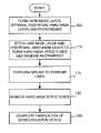
- FIG. 1illustrates an exemplary process for forming a semiconductor memory device in an implementation consistent with the principles of the invention
- FIGS. 2-10illustrate exemplary views of a semiconductor memory device fabricated according to the processing described in FIG. 1 .
- FIG. 1illustrates an exemplary process for forming a semiconductor memory device in an implementation consistent with the principles of the invention.
- the semiconductor memory deviceincludes a core memory array of a flash memory device.
- FIGS. 2-10illustrate exemplary views of a semiconductor memory device fabricated according to the processing described in FIG. 1 .
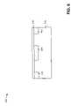
- processingmay begin with a semiconductor device 200 that includes a layer 210 (or an area 210 ).
- layer 210may be any appropriately selected semiconductor substrate known in the art.
- layer 210may comprise silicon or other semiconducting materials, such as germanium, or combinations of semiconducting materials, such as silicon-germanium.
- layer 210may include a layer of material formed one or more layers above the semiconductor substrate.
- area 210may represent a group of memory cells formed in a core area of a memory array. In this implementation, the subsequent processing described below may be performed to facilitate forming source/drain junctions for each memory cell.
- a hard mask layer 220may be formed on layer 210 in a well-known manner (act 105 ). In one implementation consistent with the principles of the invention, hard mask layer 220 may be formed on layer 210 to a thickness ranging from about 500 ⁇ to about 5000 ⁇ . Hard mask layer 220 may comprise, for example, amorphous carbon, SiLK, other materials that comprise carbon or a polymer, etc.
- An optional additional hard mask layer 230may be formed on hard mask layer 220 (act 105 ).
- additional hard mask layer 230may be formed on hard mask layer 220 to a thickness ranging from about 100 ⁇ to about 3,000 ⁇ .
- Additional hard mask layer 230may comprise an anti-reflective coating (ARC) or other types of materials, such as SiON, SiOC, an oxide, or a silicon nitride.
- ARCanti-reflective coating
- a photoresist materialmay be patterned and etched to form masks 240 on the top surface of additional hard mask layer 230 (act 105 ).
- Masks 240may be used to facilitate formation of one or hard mask structures on semiconductor device 200 , as described in more detail below.
- the width of each mask 240may range from about 450 ⁇ to about 1,200 ⁇ .
- the pitchi.e., the center-to-center distance between masks 240 may range from about 900 ⁇ to about 2,400 ⁇ ).
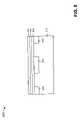
- Semiconductor device 200may then be etched, as illustrated in FIG. 3 (act 110 ).
- layers 220 and 230may be etched in a conventional manner with the etching terminating at layer 210 , thereby forming hard mask structures 310 .
- Photoresist mask 240may be removed during the etching of layers 220 and 230 (act 110 ).
- the width of hard mask structures 310may be substantially similar to the width of masks 240 (i.e., the width of each hard mask structure 310 may range from about 450 ⁇ to about 1,200 ⁇ ).
- the pitch of mask structures 310may also be substantially similar to the pitch of masks 240 (e.g., about 900 ⁇ to about 2,400 ⁇ ).
- hard mask structures 310have a substantially rectangular cross-sectional shape, as opposed to masks 240 which exhibit rounding at the top portions. Having this uniform rectangular shape enables structures 310 to facilitate more precisely formed source/drain junction profiles for semiconductor device 200 .
- Source/drain junctions or bit lines 410 for a subsequently (or previously) formed memory arraymay be formed, as illustrated in FIG. 4 , in the areas between hard mask structures 310 (act 115 ).
- bit lines 410may be formed by a main perpendicular implant process.
- the main perpendicular implantmay be a relatively high concentration implant that is capable of producing bit lines 410 .
- a p-type dopantsuch as boron, may be used as the dopant.
- the p-type dopant atomsmay be implanted at a dosage of about 1 ⁇ 10 13 atoms/cm 2 to about 1 ⁇ 10 15 atoms/cm 2 and an implantation energy of about 4 KeV to about 40 KeV, which may depend on the desired junction depth for bit lines 410 .
- an n-type dopantsuch as arsenic or phosphorous, may be used as the dopant.
- the n-type dopant atomsmay be implanted at a dosage of about 1 ⁇ 10 13 atoms/cm 2 to about 1 ⁇ 10 15 atoms/cm 2 and an implantation energy of about 4 KeV to about 40 KeV, which may depend on the desired junction depth for bit lines 410 .
- the junction profile of bit lines 410may be precisely controlled.
- the junction profile of bit lines 410may be substantially aligned with the side surfaces of hard mask structures 310 and may have a substantially rectangular shape. That is, the ions are substantially blocked from penetrating beneath structures hard mask structures 310 , resulting in a desired junction profile between hard mask structures 310 .
- Bit lines 410may, for example, be formed to a width (W) ranging from about 200 ⁇ to about 600 ⁇ and a depth (D) ranging from about 200 ⁇ to about 3,000 ⁇ .
- Hard mask structures 310may be removed, as illustrated in FIG. 5 (act 120 ). Processing may then continue with the completion of memory cell fabrication (act 125 ). It will be appreciated that in other implementations consistent with the principles of the invention, one or more of the following acts may be performed prior to the formation of bit lines 410 described above.
- area 210may represent a memory cell array.
- Each memory cellfor example, may be formed by forming a dielectric layer 610 , such as a silicon oxide layer, on device 200 , as illustrated in FIG. 6 .
- dielectric layer 610may comprise SiO 2 and may be deposited using chemical vapor deposition (CVD) (or thermally grown) to a thickness ranging from about 50 ⁇ to about 200 ⁇ . It will be appreciated that dielectric layer 610 may comprise other materials that may be deposited or grown.
- a charge storage layer 710may be formed on dielectric layer 610 , as illustrated in FIG. 7 .
- charge storage layer 710may be formed, for example, from a non-conductive material, such as a silicon nitride material, a silicon oxide material, or another dielectric material, and may be deposited to a thickness ranging from about 50 ⁇ to about 500 ⁇ .
- a dielectric layer 810may be formed on charge storage layer 710 , as illustrated in FIG. 8 .
- dielectric layer 810may comprise silicon dioxide or another material formed to a thickness ranging from about 30 ⁇ to about 200 ⁇ .
- a polysilicon layermay be deposited, patterned, and etched to form word line 910 over dielectric layer 810 , as illustrated in FIG. 9 .
- word line 910may function as a control gate electrode.
- the polysilicon layermay be deposited to a thickness ranging from about 500 ⁇ to about 3,000 ⁇ .
- Semiconductor device 200 illustrated in FIG. 9may be a silicon-oxide-nitride-oxide-silicon (SONOS) type memory device, with layer 710 acting as a charge storage element for each memory cell of the memory device.
- Each memory cellmay be an EEPROM type memory device and one or more programming circuits (not shown) may be used to facilitate programming and erasing of one or more memory cells of semiconductor device 200 .
- each memory cell of semiconductor device 200may be configured to store two bits of data (labeled 1010 and 1020 ), as illustrated in FIG. 10 . That is, charge storage layer 710 may be programmed to store two separate bits of data 1010 and 1020 by localizing the first and second charges to the respective left and right sides of charge storage layer 710 , as illustrated in FIG. 10 .
- charge storage layer 710may be programmed to store two separate bits of data 1010 and 1020 by localizing the first and second charges to the respective left and right sides of charge storage layer 710 , as illustrated in FIG. 10 .
- each of the two bits 1010 and 1020 of a memory cellmay be programmed independently by, for example, channel hot electron injection, to store a bit on each respective side of the charge storage layer 710 . In this manner, the charges in charge storage layer 710 become effectively trapped on each respective side of charge storage layer 710 . Erasing of each bit in the memory cell may also be performed independently. During erasing, the bits stored in charge storage layer 710
- a dielectric layer(not shown) may be deposited over semiconductor device 200 .
- the dielectric layermay act as an inter-layer dielectric (ILD) for semiconductor device 200 .
- the ILDmay include, for example, a phosphosilicate glass (PSG) material, a boro-phosphosilicate (BSPG) material, an oxide or some other dielectric material.
- PSGphosphosilicate glass
- BSPGboro-phosphosilicate
- the ILDmay optionally be planarized using a conventional process, such as a chemical-mechanical polishing (CMP) process.
- CMPchemical-mechanical polishing
- the CMP processmay planarize the top surface of the ILD to facilitate formation of subsequent structures, such as interconnect lines.
- the ILDfunctions to isolate various conductive structures, such as various interconnect lines (not shown) or bit lines 410 from an external electrode, etc.
- a trench(not shown) may subsequently be formed in the ILD using conventional photolithographic and etching techniques.
- the trenchmay be used to form a contact to, for example, a bit line 410 .
- a metal layersuch as copper or aluminum, may be deposited to fill the trench.
- An interconnect linemay be formed over the planarized top surface of the ILD.
- a metalsuch as copper or aluminum, may be deposited to form an interconnect that connects various features in semiconductor device 200 , such as bit lines 410 to an external electrode, to facilitate programming or erasing the various memory cells in semiconductor device 200 .
- disposable hard mask structuresmay be used in the fabrication of a semiconductor memory device to precisely control the junction profile, thereby improving the performance of the memory device.
Landscapes
- Physics & Mathematics (AREA)
- High Energy & Nuclear Physics (AREA)
- Engineering & Computer Science (AREA)
- Health & Medical Sciences (AREA)
- Toxicology (AREA)
- Condensed Matter Physics & Semiconductors (AREA)
- General Physics & Mathematics (AREA)
- Manufacturing & Machinery (AREA)
- Computer Hardware Design (AREA)
- Microelectronics & Electronic Packaging (AREA)
- Power Engineering (AREA)
- Semiconductor Memories (AREA)
Abstract
Description
Claims (19)
Priority Applications (1)
| Application Number | Priority Date | Filing Date | Title |
|---|---|---|---|
| US11/100,563US7341956B1 (en) | 2005-04-07 | 2005-04-07 | Disposable hard mask for forming bit lines |
Applications Claiming Priority (1)
| Application Number | Priority Date | Filing Date | Title |
|---|---|---|---|
| US11/100,563US7341956B1 (en) | 2005-04-07 | 2005-04-07 | Disposable hard mask for forming bit lines |
Publications (1)
| Publication Number | Publication Date |
|---|---|
| US7341956B1true US7341956B1 (en) | 2008-03-11 |
Family
ID=39155322
Family Applications (1)
| Application Number | Title | Priority Date | Filing Date |
|---|---|---|---|
| US11/100,563Active2026-04-13US7341956B1 (en) | 2005-04-07 | 2005-04-07 | Disposable hard mask for forming bit lines |
Country Status (1)
| Country | Link |
|---|---|
| US (1) | US7341956B1 (en) |
Cited By (3)
| Publication number | Priority date | Publication date | Assignee | Title |
|---|---|---|---|---|
| US20060292800A1 (en)* | 2005-06-23 | 2006-12-28 | Yen-Hao Shih | ONO formation of semiconductor memory device and method of fabricating the same |
| EP3041031A1 (en)* | 2014-12-30 | 2016-07-06 | IMEC vzw | A method of providing an implanted region in a semiconductor structure |
| CN114743867A (en)* | 2022-06-13 | 2022-07-12 | 合肥新晶集成电路有限公司 | Semiconductor structure and preparation method thereof |
Citations (22)
| Publication number | Priority date | Publication date | Assignee | Title |
|---|---|---|---|---|
| US5753557A (en)* | 1996-10-07 | 1998-05-19 | Vanguard International Semiconductor Company | Bridge-free self aligned silicide process |
| US6171940B1 (en)* | 1999-10-01 | 2001-01-09 | United Microelectronics Corp. | Method for fabricating semiconductor devices having small dimension gate structures |
| EP1170800A2 (en) | 2000-07-03 | 2002-01-09 | Sharp Kabushiki Kaisha | Nonvolatile semiconductor memory device, process of manufacturing the same and method of operating the same |
| US20020086547A1 (en)* | 2000-02-17 | 2002-07-04 | Applied Materials, Inc. | Etch pattern definition using a CVD organic layer as an anti-reflection coating and hardmask |
| DE10110150A1 (en) | 2001-03-02 | 2002-09-19 | Infineon Technologies Ag | Method for producing metallic bit lines for memory cell arrays, method for producing memory cell arrays and memory cell array |
| US20030096503A1 (en)* | 2001-10-15 | 2003-05-22 | Cho Sung Yoon | Method of fabricating a semiconductor device |
| US6576562B2 (en)* | 2000-12-15 | 2003-06-10 | Kabushiki Kaisha Toshiba | Manufacturing method of semiconductor device using mask pattern having high etching resistance |
| US6605541B1 (en)* | 1998-05-07 | 2003-08-12 | Advanced Micro Devices, Inc. | Pitch reduction using a set of offset masks |
| US6607955B2 (en)* | 1998-07-13 | 2003-08-19 | Samsung Electronics Co., Ltd. | Method of forming self-aligned contacts in a semiconductor device |
| US6620741B1 (en) | 2002-06-10 | 2003-09-16 | Intel Corporation | Method for controlling etch bias of carbon doped oxide films |
| US20040005778A1 (en)* | 2002-06-14 | 2004-01-08 | Matthias Kronke | Method for structuring a silicon layer |
| US20040058518A1 (en) | 2002-09-23 | 2004-03-25 | Infineon Technologies North America Corp. | Method of forming organic spacers and using organic spacers to form semiconductor device features |
| US6764903B1 (en)* | 2003-04-30 | 2004-07-20 | Taiwan Semiconductor Manufacturing Co., Ltd | Dual hard mask layer patterning method |
| US6797565B1 (en) | 2002-09-16 | 2004-09-28 | Advanced Micro Devices, Inc. | Methods for fabricating and planarizing dual poly scalable SONOS flash memory |
| US6864556B1 (en)* | 2002-07-31 | 2005-03-08 | Advanced Micro Devices, Inc. | CVD organic polymer film for advanced gate patterning |
| US20050136630A1 (en) | 2003-12-23 | 2005-06-23 | Kim In S. | Methods of forming a pattern for a semiconductor device |
| US6927145B1 (en) | 2004-02-02 | 2005-08-09 | Advanced Micro Devices, Inc. | Bitline hard mask spacer flow for memory cell scaling |
| US20050212035A1 (en) | 2002-08-30 | 2005-09-29 | Fujitsu Amd Semiconductor Limited | Semiconductor storage device and manufacturing method thereof |
| US20060030151A1 (en) | 2004-08-09 | 2006-02-09 | Applied Materials, Inc. | Sputter deposition and etching of metallization seed layer for overhang and sidewall improvement |
| US7037850B2 (en)* | 2003-04-04 | 2006-05-02 | Hynix Semiconductor Inc. | Method for fabricating semiconductor device with fine patterns |
| US20060154477A1 (en)* | 2005-01-12 | 2006-07-13 | Quain Geng | Polymer spacer formation |
| US20060264002A1 (en)* | 2004-08-31 | 2006-11-23 | Luan Tran | Methods for increasing photo-alignment margins |
- 2005
- 2005-04-07USUS11/100,563patent/US7341956B1/enactiveActive
Patent Citations (22)
| Publication number | Priority date | Publication date | Assignee | Title |
|---|---|---|---|---|
| US5753557A (en)* | 1996-10-07 | 1998-05-19 | Vanguard International Semiconductor Company | Bridge-free self aligned silicide process |
| US6605541B1 (en)* | 1998-05-07 | 2003-08-12 | Advanced Micro Devices, Inc. | Pitch reduction using a set of offset masks |
| US6607955B2 (en)* | 1998-07-13 | 2003-08-19 | Samsung Electronics Co., Ltd. | Method of forming self-aligned contacts in a semiconductor device |
| US6171940B1 (en)* | 1999-10-01 | 2001-01-09 | United Microelectronics Corp. | Method for fabricating semiconductor devices having small dimension gate structures |
| US20020086547A1 (en)* | 2000-02-17 | 2002-07-04 | Applied Materials, Inc. | Etch pattern definition using a CVD organic layer as an anti-reflection coating and hardmask |
| EP1170800A2 (en) | 2000-07-03 | 2002-01-09 | Sharp Kabushiki Kaisha | Nonvolatile semiconductor memory device, process of manufacturing the same and method of operating the same |
| US6576562B2 (en)* | 2000-12-15 | 2003-06-10 | Kabushiki Kaisha Toshiba | Manufacturing method of semiconductor device using mask pattern having high etching resistance |
| DE10110150A1 (en) | 2001-03-02 | 2002-09-19 | Infineon Technologies Ag | Method for producing metallic bit lines for memory cell arrays, method for producing memory cell arrays and memory cell array |
| US20030096503A1 (en)* | 2001-10-15 | 2003-05-22 | Cho Sung Yoon | Method of fabricating a semiconductor device |
| US6620741B1 (en) | 2002-06-10 | 2003-09-16 | Intel Corporation | Method for controlling etch bias of carbon doped oxide films |
| US20040005778A1 (en)* | 2002-06-14 | 2004-01-08 | Matthias Kronke | Method for structuring a silicon layer |
| US6864556B1 (en)* | 2002-07-31 | 2005-03-08 | Advanced Micro Devices, Inc. | CVD organic polymer film for advanced gate patterning |
| US20050212035A1 (en) | 2002-08-30 | 2005-09-29 | Fujitsu Amd Semiconductor Limited | Semiconductor storage device and manufacturing method thereof |
| US6797565B1 (en) | 2002-09-16 | 2004-09-28 | Advanced Micro Devices, Inc. | Methods for fabricating and planarizing dual poly scalable SONOS flash memory |
| US20040058518A1 (en) | 2002-09-23 | 2004-03-25 | Infineon Technologies North America Corp. | Method of forming organic spacers and using organic spacers to form semiconductor device features |
| US7037850B2 (en)* | 2003-04-04 | 2006-05-02 | Hynix Semiconductor Inc. | Method for fabricating semiconductor device with fine patterns |
| US6764903B1 (en)* | 2003-04-30 | 2004-07-20 | Taiwan Semiconductor Manufacturing Co., Ltd | Dual hard mask layer patterning method |
| US20050136630A1 (en) | 2003-12-23 | 2005-06-23 | Kim In S. | Methods of forming a pattern for a semiconductor device |
| US6927145B1 (en) | 2004-02-02 | 2005-08-09 | Advanced Micro Devices, Inc. | Bitline hard mask spacer flow for memory cell scaling |
| US20060030151A1 (en) | 2004-08-09 | 2006-02-09 | Applied Materials, Inc. | Sputter deposition and etching of metallization seed layer for overhang and sidewall improvement |
| US20060264002A1 (en)* | 2004-08-31 | 2006-11-23 | Luan Tran | Methods for increasing photo-alignment margins |
| US20060154477A1 (en)* | 2005-01-12 | 2006-07-13 | Quain Geng | Polymer spacer formation |
Non-Patent Citations (2)
| Title |
|---|
| 2002 IEEE International Solid-State Circuits Conference, 29 pages. |
| 2002 IEEE International Solid-State Circuits Conference, Session 6, "SRAM and Non-Volatile Memories," Feb. 4, 2004,6pages. |
Cited By (4)
| Publication number | Priority date | Publication date | Assignee | Title |
|---|---|---|---|---|
| US20060292800A1 (en)* | 2005-06-23 | 2006-12-28 | Yen-Hao Shih | ONO formation of semiconductor memory device and method of fabricating the same |
| US7763935B2 (en)* | 2005-06-23 | 2010-07-27 | Macronix International Co., Ltd. | ONO formation of semiconductor memory device and method of fabricating the same |
| EP3041031A1 (en)* | 2014-12-30 | 2016-07-06 | IMEC vzw | A method of providing an implanted region in a semiconductor structure |
| CN114743867A (en)* | 2022-06-13 | 2022-07-12 | 合肥新晶集成电路有限公司 | Semiconductor structure and preparation method thereof |
Similar Documents
| Publication | Publication Date | Title |
|---|---|---|
| US12262539B2 (en) | 3D NAND memory device and method of forming the same | |
| US8497555B2 (en) | Vertical memory devices including indium and/or gallium channel doping | |
| CN100405582C (en) | Charge trap memory device and manufacturing method thereof | |
| US7670959B2 (en) | Memory device etch methods | |
| US8314454B2 (en) | Local interconnect having increased misalignment tolerance | |
| US7341956B1 (en) | Disposable hard mask for forming bit lines | |
| US7498222B1 (en) | Enhanced etching of a high dielectric constant layer | |
| US7972948B2 (en) | Method for forming bit lines for semiconductor devices | |
| US8404541B2 (en) | Strapping contact for charge protection | |
| US6750100B2 (en) | Nano-meter memory device and method of making the same | |
| US7285499B1 (en) | Polymer spacers for creating sub-lithographic spaces | |
| US8203178B2 (en) | System and method for reducing process-induced charging | |
| US7167398B1 (en) | System and method for erasing a memory cell | |
| CN102479787B (en) | Semiconductor integrated circuit device and manufacturing method, and layout of semiconductor memory device | |
| US7561457B2 (en) | Select transistor using buried bit line from core | |
| US7704878B2 (en) | Contact spacer formation using atomic layer deposition | |
| US7476604B1 (en) | Aggressive cleaning process for semiconductor device contact formation | |
| US7238571B1 (en) | Non-volatile memory device with increased reliability |
Legal Events
| Date | Code | Title | Description |
|---|---|---|---|
| AS | Assignment | Owner name:SPANSION LLC, CALIFORNIA Free format text:ASSIGNMENT OF ASSIGNORS INTEREST;ASSIGNORS:TOKUNO, HIROKAZU;NGO, MINH-VAN;CHEN, CINTI XIAOHUA;REEL/FRAME:016459/0122;SIGNING DATES FROM 20050315 TO 20050316 Owner name:ADVANCED MICRO DEVICES, INC., CALIFORNIA Free format text:ASSIGNMENT OF ASSIGNORS INTEREST;ASSIGNOR:HUI, ANGELA T.;REEL/FRAME:016459/0117 Effective date:20050316 | |
| FEPP | Fee payment procedure | Free format text:PAYOR NUMBER ASSIGNED (ORIGINAL EVENT CODE: ASPN); ENTITY STATUS OF PATENT OWNER: LARGE ENTITY | |
| STCF | Information on status: patent grant | Free format text:PATENTED CASE | |
| AS | Assignment | Owner name:BARCLAYS BANK PLC,NEW YORK Free format text:SECURITY AGREEMENT;ASSIGNORS:SPANSION LLC;SPANSION INC.;SPANSION TECHNOLOGY INC.;AND OTHERS;REEL/FRAME:024522/0338 Effective date:20100510 Owner name:BARCLAYS BANK PLC, NEW YORK Free format text:SECURITY AGREEMENT;ASSIGNORS:SPANSION LLC;SPANSION INC.;SPANSION TECHNOLOGY INC.;AND OTHERS;REEL/FRAME:024522/0338 Effective date:20100510 | |
| FPAY | Fee payment | Year of fee payment:4 | |
| AS | Assignment | Owner name:SPANSION LLC, CALIFORNIA Free format text:RELEASE BY SECURED PARTY;ASSIGNOR:BARCLAYS BANK PLC;REEL/FRAME:035201/0159 Effective date:20150312 Owner name:SPANSION TECHNOLOGY LLC, CALIFORNIA Free format text:RELEASE BY SECURED PARTY;ASSIGNOR:BARCLAYS BANK PLC;REEL/FRAME:035201/0159 Effective date:20150312 Owner name:SPANSION INC., CALIFORNIA Free format text:RELEASE BY SECURED PARTY;ASSIGNOR:BARCLAYS BANK PLC;REEL/FRAME:035201/0159 Effective date:20150312 | |
| AS | Assignment | Owner name:MORGAN STANLEY SENIOR FUNDING, INC., NEW YORK Free format text:SECURITY INTEREST;ASSIGNORS:CYPRESS SEMICONDUCTOR CORPORATION;SPANSION LLC;REEL/FRAME:035240/0429 Effective date:20150312 | |
| FPAY | Fee payment | Year of fee payment:8 | |
| AS | Assignment | Owner name:SPANSION LLC, CALIFORNIA Free format text:ASSIGNMENT OF ASSIGNORS INTEREST;ASSIGNOR:ADVANCED MICRO DEVICES, INC.;REEL/FRAME:042416/0448 Effective date:20170509 | |
| AS | Assignment | Owner name:MONTEREY RESEARCH, LLC, CALIFORNIA Free format text:ASSIGNMENT OF ASSIGNORS INTEREST;ASSIGNOR:CYPRESS SEMICONDUCTOR CORPORATION;REEL/FRAME:044051/0244 Effective date:20170928 Owner name:SPANSION LLC, CALIFORNIA Free format text:RELEASE BY SECURED PARTY;ASSIGNOR:MORGAN STANLEY SENIOR FUNDING, INC.;REEL/FRAME:044052/0280 Effective date:20170928 Owner name:CYPRESS SEMICONDUCTOR CORPORATION, CALIFORNIA Free format text:RELEASE BY SECURED PARTY;ASSIGNOR:MORGAN STANLEY SENIOR FUNDING, INC.;REEL/FRAME:044052/0280 Effective date:20170928 | |
| AS | Assignment | Owner name:MONTEREY RESEARCH, LLC, CALIFORNIA Free format text:ASSIGNMENT OF ASSIGNORS INTEREST;ASSIGNOR:CYPRESS SEMICONDUCTOR CORPORATION;REEL/FRAME:044094/0669 Effective date:20170928 | |
| AS | Assignment | Owner name:CYPRESS SEMICONDUCTOR CORPORATION, CALIFORNIA Free format text:ASSIGNMENT OF ASSIGNORS INTEREST;ASSIGNOR:SPANSION LLC;REEL/FRAME:049898/0001 Effective date:20150601 | |
| MAFP | Maintenance fee payment | Free format text:PAYMENT OF MAINTENANCE FEE, 12TH YEAR, LARGE ENTITY (ORIGINAL EVENT CODE: M1553); ENTITY STATUS OF PATENT OWNER: LARGE ENTITY Year of fee payment:12 | |
| AS | Assignment | Owner name:MORGAN STANLEY SENIOR FUNDING, INC., NEW YORK Free format text:CORRECTIVE ASSIGNMENT TO CORRECT THE 8647899 PREVIOUSLY RECORDED ON REEL 035240 FRAME 0429. ASSIGNOR(S) HEREBY CONFIRMS THE SECURITY INTERST;ASSIGNORS:CYPRESS SEMICONDUCTOR CORPORATION;SPANSION LLC;REEL/FRAME:058002/0470 Effective date:20150312 |