US7339241B2 - FinFET structure with contacts - Google Patents
FinFET structure with contactsDownload PDFInfo
- Publication number
- US7339241B2 US7339241B2US11/216,974US21697405AUS7339241B2US 7339241 B2US7339241 B2US 7339241B2US 21697405 AUS21697405 AUS 21697405AUS 7339241 B2US7339241 B2US 7339241B2
- Authority
- US
- United States
- Prior art keywords
- current electrode
- fin
- gate
- horizontal direction
- electrode portion
- Prior art date
- Legal status (The legal status is an assumption and is not a legal conclusion. Google has not performed a legal analysis and makes no representation as to the accuracy of the status listed.)
- Expired - Fee Related, expires
Links
Images

Classifications
- H—ELECTRICITY
- H10—SEMICONDUCTOR DEVICES; ELECTRIC SOLID-STATE DEVICES NOT OTHERWISE PROVIDED FOR
- H10D—INORGANIC ELECTRIC SEMICONDUCTOR DEVICES
- H10D30/00—Field-effect transistors [FET]
- H10D30/60—Insulated-gate field-effect transistors [IGFET]
- H10D30/62—Fin field-effect transistors [FinFET]
- H—ELECTRICITY
- H10—SEMICONDUCTOR DEVICES; ELECTRIC SOLID-STATE DEVICES NOT OTHERWISE PROVIDED FOR
- H10D—INORGANIC ELECTRIC SEMICONDUCTOR DEVICES
- H10D30/00—Field-effect transistors [FET]
- H10D30/60—Insulated-gate field-effect transistors [IGFET]
- H10D30/67—Thin-film transistors [TFT]
- H10D30/6729—Thin-film transistors [TFT] characterised by the electrodes
Definitions
- This inventionrelates to FinFETs, and more particularly to FinFETs with contacts.
- FinFET technologyhas shown great promise in improving transistor density and reduced source/drain leakage while maintaining needed performance requirements.
- Thisuses a semiconductor structure elevated above a substrate floor.
- the channel portionitself resembles a fin so the name FinFET has been used.
- a gateoverlies the fin and the width of the gate in this structure determines the channel length.
- the height of the fin and the number of finsdetermines the channel width. This results in improved density.
- the gateis effective on two sides of the fin resulting in two channels for each fin.
- the finis also sufficiently thin that the entire thickness of the fin is under the influence of the gate. This results in reduced source/drain leakage.
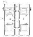
- FIG. 1is a top view of a FinFET useful in demonstrating a problem that has been discovered in performance and manufacturability;
- FIG. 2is a cross section of the FinFET of FIG. 1 ;
- FIG. 3is a top view of a FinFET according to an embodiment of the invention.
- FIG. 4is a cross section of the FinFET of FIG. 3 taken at one location;
- FIG. 5is a cross section of the FinFET of FIG. 3 taken at another location.
- FIG. 6is a top view of a FinFET according to an alternative embodiment.
- a FinFETwhich by its nature has both elevated source/drains and an elevated channel that are part of an elevated semiconductor portion that has parallel fins and one source/drain on one side of the fins and another source/drain on the other side of the fins, has all of the source/drains contacts away from the fins as much as reasonably possible.
- the gate contactsextend upward from the top surface of the elevated semiconductor portion.
- the gatealso extends upward from the top surface of the elevated semiconductor portion.
- the contactsare located between the fins where the gate is below the height of the elevated semiconductor portion so the contacts are as far as reasonably possible from the gate, thereby reducing gate to drain capacitance and providing additional assistance to alignment tolerance.
- FIG. 1Shown in FIG. 1 is a FinFET structure 10 , a type of semiconductor device, shown from a top view comprising an elevated semiconductor portion 12 having a source/drain region 22 on one side, a source/drain region 24 on the other side, and semiconductor fins 26 , 28 , and 30 .
- Source/drain regionscan be considered current electrodes.
- the elevated source/drains plus finscan be considered a semiconductor structure. Since increasing the number of fins is the way of increasing the effective channel width, in any integrated circuit with FinFETs, transistors will typically have multiple fins.
- On source/drain region 22are contacts 14 and 16 .
- On source/drain region 24are contacts 18 and 20 .
- Contacts 14 , 16 , 18 , and 20by making physical contact, make electrical contact.
- a gate 32runs over and between fins 26 , 28 , and 30 .
- Contacts 14 , 16 , 18 , and 20are not perfectly vertical but extend outward as they rise. While problems exist for vertical contacts, these problems are exacerbated as the contacts become more tapered.
- elevated semiconductor portion 12is silicon, but other semiconductor materials could be used.
- Contacts 14 , 16 , 18 , and 20are preferably tungsten with a silicide bottom to interface with elevated semiconductor portion 12 . The silicide bottoms are formed by siliciding the source/drains. Metal is then applied in holes over the silicide regions to make physical contact with these silicide regions and complete the contact formation.
- the upper dimension of contact 14is an area 17 which tapers to a lower dimension shown as area 15 .
- Area 15resides on the silicided portion of the source/drain region 22 .
- the contactscould simply be considered the region between the upper dimension and the lower dimension and the silicided region could be considered separate from the contact.
- Gate 32is preferably polysilicon because of the very conformal deposition characteristic of polysilicon. Other materials may also be used, especially metal if it can in fact be deposited effectively.
- the particular dimensions of the featureswill vary based on the particular technology being used and the design choices. The dimensions used in this example are as follows:
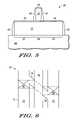
- FIG. 2Shown in FIG. 2 is FinFET structure 10 in a cross section taken through contacts 14 and 18 and fin 26 .
- FIG. 2shows that elevated semiconductor portion 12 is on a substrate 38 .
- Substrate 38is preferably an insulator such as silicon oxide.
- the top surface of substrate 38is considered horizontal so that any direction parallel to the top surface of substrate 38 is also considered horizontal.
- gate contacts 14 and 18angularly become closer to gate 32 as they rise from elevated semiconductor portion 12 . This shows the lower dimension 15 of contact 14 being smaller than an upper dimension 17 of contact 14 .
- the portion of the contacts with the lower dimensionis considered the base of the contact.
- a capacitance C 1is present between gate 32 and contact 14 .
- a capacitance C 2is present between gate 32 and contact 18 .
- Both capacitance C 1 and C 2add capacitive loading on the gate, which is an adverse effect.
- Gate to drain capacitancehas an effect that is generally even more adverse. Assuming source/drain region 22 acts as the drain in a particular application, capacitance C 1 increases the gate to drain capacitance.
- the voltage change on the gatecauses a change in voltage in the opposite direction on the drain. It is the speed with which the drain voltage responds to a change in gate voltage that determines the speed of operation.
- capacitance C 1works against this desired change because its effect is to move the drain voltage in the same direction as the gate voltage in opposition to the desired opposite direction.
- gate 32with misalignment of contacts 14 and 18 as well as gate 32 , the gate can come very close to one of contacts 14 and 18 . This could become a leakage point or an exceedingly high adverse gate to drain capacitance. In viewing FIGS. 1 and 2 together, this close edge of gate 32 to contacts 14 and 18 is for the whole width of fin 26 .
- This alignment of contacts 14 and 18 with fin 26maximizes capacitance and the risk of misalignment becoming a problem. This alignment is a natural alignment based on the general concept of placing the contact facing the channel, but even if the contacts are randomly placed, this would occur often.
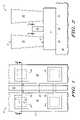
- FIG. 3Shown in FIG. 3 is a FinFET structure 40 similar to FinFET 10 of FIG. 1 with differently placed contacts to avoid or reduce the negative impact of the contact placement used in FinFET 10 .
- the elements that are the sameretain the same numbers.
- contact to source/drain region 22is made by contacts 44 and 46 being on source/drain region 22 .
- Contact to source/drain region 24is made by contact 48 and other contacts only partially shown.
- Contacts 44 , 46 , and 48are of same construction as contacts 14 and 16 but placed differently.
- contact 44exemplary of all of the contacts in this regard, has a lower dimension and an area 52 and a larger upper dimension of an area 54 .
- an additional fin 42is present and shown as being adjacent to fin 26 .
- Contact 44is centered between fins 42 and 26 .
- Contact 46is centered between fins 28 and 30 , which are also adjacent fins. Although centering is desired, it is not perfectly achieved in an actual manufacturing context, especially repeatably. Accordingly, centered in this context means that it is centered using a reasonable application of the design and manufacturing constraints used in implementing the structure.
- FIG. 4Shown in FIG. 4 is a cross section taken through the middle of contact 44 and between fins 42 and 26 . This shows sidewall spacers 60 around gate 32 and sidewall spacer 62 around source/drain regions 22 and 24 . Shown in FIG. 4 also is a silicide layer 56 that is over source/drain regions 22 and 24 and gate 32 . Silicide layer 56 forms part of contact 44 . This FIG. 4 shows that contact 44 is adjacent to gate 32 where gate 32 is between fins 42 and 26 so that gate 32 is below contact 44 .
- the gate height in this exampleis the same as the fin and source/drain height. This shows that there is a much greater overall distance between contact 44 and gate 32 in the area between fins 42 and 26 than between gate 32 and contact 14 in FIG. 2 .
- FIG. 4there is less capacitance for the case shown in FIG. 4 .
- the contacts for source/drain region 22are staggered with respect to the contacts for source/drain 24 . This provides for more flexibility in making connections to the two source/drain regions 22 and 24 . In this way, for example, parallel interconnect lines could run across FinFET structure 40 in the direction of the fins and separately contact source/drain regions 22 and 24 .
- FIG. 5Shown in FIG. 5 is a cross section through the middle of fin 26 .
- FIG. 5shows that there are no contacts adjacent to gate 32 where gate 32 is raised over fin 26 .
- the area where gate 32 rises over the finis where the particular vulnerability to increased capacitance and problems associated with misalignment occur.
- the corner of contact 44 closest to fin 26is relatively close to gate 32 as it rises over fin 26 .
- This is a relatively small area for increasing capacitanceso the capacitance added at this corner is small compared to the capacitance added by contact 14 being along the whole side of fin 26 and thus the whole side of gate 32 that passes over fin 26 .
- the corners of structuresare rounded in actual manufacturing. Thus, there is actually more distance from the corner of contact 44 to the raised portion of gate 32 over fin 26 than it would appear from FIG. 3 .
- finsare at different angle than a 90 degree angle to the source/drain regions.
- the point at which the gate rises over the finwill be somewhat offset from the point at which the fin intersects the source/drain region.
- the area where it is desirable to avoid having the contactis aligned to that region where the gate is over the fin.
- FIG. 6An example is shown in which there is a FinFET structure 70 having an elevated semiconductor region 71 having a source/drain region 72 , a source/drain region 73 , and a fin 76 between source/drain regions 72 and 73 . This shows fin 76 at angle to source/drain regions that is not 90 degrees. This is preferable when a particular crystal orientation is desired for a transistor type.
- N channel transistors and P channel transistorsmay be optimized for performance using a different crystal orientation for the channel.
- a gate 78overlies fin 76 . Where gate 78 crosses fin 76 is the area where adjacent contact placement should be avoided. Extending perpendicular to source/drain region 72 are dotted lines extending from the points where gate 78 crosses over fin 76 . These dotted lines define an area 80 on source/drain region 72 between them where a contact should be avoided. An “X” is placed in this area to show the region where contact should be avoided. Thus a contact should be centered between these areas along a given source/drain.
- a similar region 82 on source/drain region 73 orthogonally aligned to the elevated portion of gate 78should not have a contact.
- FIGS. 3-5 and FIG. 6This characterization is the same as for the orthogonal fin case shown in FIGS. 3-5 , it is just that the “no-contact” area is the same as the area adjacent to the fin in those cases. But in both cases, FIGS. 3-5 and FIG. 6 , it is the area in the source/drain region orthogonal to the sidewall of the portion of the gate that is over the fin that is the no-contact area. This portion of the source/drain region that is orthogonally adjacent to the elevated portion of the gate is considered a gate adjacent area. Thus the contacts should be placed between the boundaries of the gate adjacent areas. The actual portion of the contact that contacts the source/drain region is the base so it the base that is between the gate adjacent areas.
- the contactsare completely outside of the gate adjacent areas, but there may be situations in which the contact is too big to achieve that. In such case it would still be preferable to minimize the encroachment into the gate adjacent areas so centering between the gate adjacent areas would be preferable.
- Source/drainsare also called current electrodes.
- a fin with source/drainsis a semiconductor structure.
Landscapes
- Insulated Gate Type Field-Effect Transistor (AREA)
- Thin Film Transistor (AREA)
Abstract
Description
- Fin height: 100 nanometers (nm)
- Gate width: 40 nm
- Fin pitch: 140 nm
- Source/drain width: 150 nm
- Contact lower dimension: 90×90 nm
- Contact upper dimension: 120×120 nm
- Fin length (between source/drain regions): 80 nm
- Fin width: 20 nm
- Gate height: 100 nm
Claims (11)
Priority Applications (1)
| Application Number | Priority Date | Filing Date | Title |
|---|---|---|---|
| US11/216,974US7339241B2 (en) | 2005-08-31 | 2005-08-31 | FinFET structure with contacts |
Applications Claiming Priority (1)
| Application Number | Priority Date | Filing Date | Title |
|---|---|---|---|
| US11/216,974US7339241B2 (en) | 2005-08-31 | 2005-08-31 | FinFET structure with contacts |
Publications (2)
| Publication Number | Publication Date |
|---|---|
| US20070045735A1 US20070045735A1 (en) | 2007-03-01 |
| US7339241B2true US7339241B2 (en) | 2008-03-04 |
Family
ID=37802871
Family Applications (1)
| Application Number | Title | Priority Date | Filing Date |
|---|---|---|---|
| US11/216,974Expired - Fee RelatedUS7339241B2 (en) | 2005-08-31 | 2005-08-31 | FinFET structure with contacts |
Country Status (1)
| Country | Link |
|---|---|
| US (1) | US7339241B2 (en) |
Cited By (17)
| Publication number | Priority date | Publication date | Assignee | Title |
|---|---|---|---|---|
| US7898041B2 (en)* | 2005-06-30 | 2011-03-01 | Intel Corporation | Block contact architectures for nanoscale channel transistors |
| US7989280B2 (en) | 2005-11-30 | 2011-08-02 | Intel Corporation | Dielectric interface for group III-V semiconductor device |
| US8071983B2 (en) | 2005-06-21 | 2011-12-06 | Intel Corporation | Semiconductor device structures and methods of forming semiconductor structures |
| US8084818B2 (en) | 2004-06-30 | 2011-12-27 | Intel Corporation | High mobility tri-gate devices and methods of fabrication |
| US8183646B2 (en) | 2005-02-23 | 2012-05-22 | Intel Corporation | Field effect transistor with narrow bandgap source and drain regions and method of fabrication |
| US8273626B2 (en) | 2003-06-27 | 2012-09-25 | Intel Corporationn | Nonplanar semiconductor device with partially or fully wrapped around gate electrode and methods of fabrication |
| US8294180B2 (en) | 2005-09-28 | 2012-10-23 | Intel Corporation | CMOS devices with a single work function gate electrode and method of fabrication |
| US8362566B2 (en) | 2008-06-23 | 2013-01-29 | Intel Corporation | Stress in trigate devices using complimentary gate fill materials |
| US8502351B2 (en) | 2004-10-25 | 2013-08-06 | Intel Corporation | Nonplanar device with thinned lower body portion and method of fabrication |
| US8617945B2 (en) | 2006-08-02 | 2013-12-31 | Intel Corporation | Stacking fault and twin blocking barrier for integrating III-V on Si |
| US9000489B2 (en) | 2012-10-31 | 2015-04-07 | International Business Machines Corporation | Local interconnects for field effect transistor devices |
| US9337307B2 (en) | 2005-06-15 | 2016-05-10 | Intel Corporation | Method for fabricating transistor with thinned channel |
| US20180138104A1 (en)* | 2016-11-14 | 2018-05-17 | Mediatek Inc. | Thermal via arrangement for multi-channel semiconductor device |
| US10038081B1 (en) | 2017-09-06 | 2018-07-31 | Nxp Usa, Inc. | Substrate contacts for a transistor |
| US10896857B2 (en)* | 2014-12-04 | 2021-01-19 | International Business Machines Corporation | Vertical field effect transistors |
| US11495497B2 (en)* | 2016-04-13 | 2022-11-08 | Taiwan Semiconductor Manufacturing Company Limited | FinFET switch |
| US11557474B2 (en)* | 2019-07-29 | 2023-01-17 | Asm Ip Holding B.V. | Methods for selective deposition utilizing n-type dopants and/or alternative dopants to achieve high dopant incorporation |
Families Citing this family (4)
| Publication number | Priority date | Publication date | Assignee | Title |
|---|---|---|---|---|
| US7268058B2 (en)* | 2004-01-16 | 2007-09-11 | Intel Corporation | Tri-gate transistors and methods to fabricate same |
| JP4487266B2 (en)* | 2006-08-30 | 2010-06-23 | エルピーダメモリ株式会社 | Semiconductor device |
| US9905663B2 (en) | 2016-06-24 | 2018-02-27 | International Business Machines Corporation | Fabrication of a vertical fin field effect transistor with a reduced contact resistance |
| KR102663811B1 (en)* | 2019-11-06 | 2024-05-07 | 삼성전자주식회사 | Integrated circuit device and method of manufacturing the same |
Citations (9)
| Publication number | Priority date | Publication date | Assignee | Title |
|---|---|---|---|---|
| US20020153587A1 (en)* | 2000-03-16 | 2002-10-24 | International Business Machines Corporation | Double planar gated SOI MOSFET structure |
| US6563131B1 (en)* | 2000-06-02 | 2003-05-13 | International Business Machines Corporation | Method and structure of a dual/wrap-around gate field effect transistor |
| US6765303B1 (en)* | 2003-05-06 | 2004-07-20 | Advanced Micro Devices, Inc. | FinFET-based SRAM cell |
| US20050020015A1 (en)* | 2003-07-22 | 2005-01-27 | Leo Mathew | Method for converting a planar transistor design to a vertical double gate transistor design |
| US20050026343A1 (en)* | 2003-07-28 | 2005-02-03 | Chartered Semiconductor Manufacturing Ltd. | Thyistor-based SRAM and method using quasi-planar finfet process for the fabrication thereof |
| US6885055B2 (en)* | 2003-02-04 | 2005-04-26 | Lee Jong-Ho | Double-gate FinFET device and fabricating method thereof |
| US7122412B2 (en)* | 2004-04-30 | 2006-10-17 | Taiwan Semiconductor Manufacturing Company, Ltd. | Method of fabricating a necked FINFET device |
| US20070001219A1 (en)* | 2005-06-30 | 2007-01-04 | Marko Radosavljevic | Block contact architectures for nanoscale channel transistors |
| US7163864B1 (en)* | 2000-10-18 | 2007-01-16 | International Business Machines Corporation | Method of fabricating semiconductor side wall fin |
- 2005
- 2005-08-31USUS11/216,974patent/US7339241B2/ennot_activeExpired - Fee Related
Patent Citations (11)
| Publication number | Priority date | Publication date | Assignee | Title |
|---|---|---|---|---|
| US20020153587A1 (en)* | 2000-03-16 | 2002-10-24 | International Business Machines Corporation | Double planar gated SOI MOSFET structure |
| US6483156B1 (en)* | 2000-03-16 | 2002-11-19 | International Business Machines Corporation | Double planar gated SOI MOSFET structure |
| US6563131B1 (en)* | 2000-06-02 | 2003-05-13 | International Business Machines Corporation | Method and structure of a dual/wrap-around gate field effect transistor |
| US7163864B1 (en)* | 2000-10-18 | 2007-01-16 | International Business Machines Corporation | Method of fabricating semiconductor side wall fin |
| US6885055B2 (en)* | 2003-02-04 | 2005-04-26 | Lee Jong-Ho | Double-gate FinFET device and fabricating method thereof |
| US6765303B1 (en)* | 2003-05-06 | 2004-07-20 | Advanced Micro Devices, Inc. | FinFET-based SRAM cell |
| US20050020015A1 (en)* | 2003-07-22 | 2005-01-27 | Leo Mathew | Method for converting a planar transistor design to a vertical double gate transistor design |
| US7013447B2 (en)* | 2003-07-22 | 2006-03-14 | Freescale Semiconductor, Inc. | Method for converting a planar transistor design to a vertical double gate transistor design |
| US20050026343A1 (en)* | 2003-07-28 | 2005-02-03 | Chartered Semiconductor Manufacturing Ltd. | Thyistor-based SRAM and method using quasi-planar finfet process for the fabrication thereof |
| US7122412B2 (en)* | 2004-04-30 | 2006-10-17 | Taiwan Semiconductor Manufacturing Company, Ltd. | Method of fabricating a necked FINFET device |
| US20070001219A1 (en)* | 2005-06-30 | 2007-01-04 | Marko Radosavljevic | Block contact architectures for nanoscale channel transistors |
Non-Patent Citations (3)
| Title |
|---|
| H. Aanathan et al, "FinFET SRAM-Device and Circuit Design Considerations", Quality Electronic Design, 2004. 5<SUP>th </SUP>International Symposium 2004, pp. 511-516. |
| K.G. Anil et al, "Layout Density Analysis of FinFETs", ESSDERC Conference Proceedings 2003, pp. 139-142. |
| Y. Liu et al, "Systematic Electrical Characteristics of Ideal Rectangular Cross Section SiFin Channel Double-Gate MOSFETs" IEEE Trans. On Nanotechnology, vol. 2, p. 198-204. |
Cited By (42)
| Publication number | Priority date | Publication date | Assignee | Title |
|---|---|---|---|---|
| US8273626B2 (en) | 2003-06-27 | 2012-09-25 | Intel Corporationn | Nonplanar semiconductor device with partially or fully wrapped around gate electrode and methods of fabrication |
| US8084818B2 (en) | 2004-06-30 | 2011-12-27 | Intel Corporation | High mobility tri-gate devices and methods of fabrication |
| US8502351B2 (en) | 2004-10-25 | 2013-08-06 | Intel Corporation | Nonplanar device with thinned lower body portion and method of fabrication |
| US8749026B2 (en) | 2004-10-25 | 2014-06-10 | Intel Corporation | Nonplanar device with thinned lower body portion and method of fabrication |
| US9741809B2 (en) | 2004-10-25 | 2017-08-22 | Intel Corporation | Nonplanar device with thinned lower body portion and method of fabrication |
| US10236356B2 (en) | 2004-10-25 | 2019-03-19 | Intel Corporation | Nonplanar device with thinned lower body portion and method of fabrication |
| US9190518B2 (en) | 2004-10-25 | 2015-11-17 | Intel Corporation | Nonplanar device with thinned lower body portion and method of fabrication |
| US8368135B2 (en) | 2005-02-23 | 2013-02-05 | Intel Corporation | Field effect transistor with narrow bandgap source and drain regions and method of fabrication |
| US10121897B2 (en) | 2005-02-23 | 2018-11-06 | Intel Corporation | Field effect transistor with narrow bandgap source and drain regions and method of fabrication |
| US9368583B2 (en) | 2005-02-23 | 2016-06-14 | Intel Corporation | Field effect transistor with narrow bandgap source and drain regions and method of fabrication |
| US9614083B2 (en) | 2005-02-23 | 2017-04-04 | Intel Corporation | Field effect transistor with narrow bandgap source and drain regions and method of fabrication |
| US9048314B2 (en) | 2005-02-23 | 2015-06-02 | Intel Corporation | Field effect transistor with narrow bandgap source and drain regions and method of fabrication |
| US8664694B2 (en) | 2005-02-23 | 2014-03-04 | Intel Corporation | Field effect transistor with narrow bandgap source and drain regions and method of fabrication |
| US8183646B2 (en) | 2005-02-23 | 2012-05-22 | Intel Corporation | Field effect transistor with narrow bandgap source and drain regions and method of fabrication |
| US9748391B2 (en) | 2005-02-23 | 2017-08-29 | Intel Corporation | Field effect transistor with narrow bandgap source and drain regions and method of fabrication |
| US8816394B2 (en) | 2005-02-23 | 2014-08-26 | Intel Corporation | Field effect transistor with narrow bandgap source and drain regions and method of fabrication |
| US11978799B2 (en) | 2005-06-15 | 2024-05-07 | Tahoe Research, Ltd. | Method for fabricating transistor with thinned channel |
| US9337307B2 (en) | 2005-06-15 | 2016-05-10 | Intel Corporation | Method for fabricating transistor with thinned channel |
| US9806195B2 (en) | 2005-06-15 | 2017-10-31 | Intel Corporation | Method for fabricating transistor with thinned channel |
| US8933458B2 (en) | 2005-06-21 | 2015-01-13 | Intel Corporation | Semiconductor device structures and methods of forming semiconductor structures |
| US8581258B2 (en) | 2005-06-21 | 2013-11-12 | Intel Corporation | Semiconductor device structures and methods of forming semiconductor structures |
| US9761724B2 (en) | 2005-06-21 | 2017-09-12 | Intel Corporation | Semiconductor device structures and methods of forming semiconductor structures |
| US9385180B2 (en) | 2005-06-21 | 2016-07-05 | Intel Corporation | Semiconductor device structures and methods of forming semiconductor structures |
| US8071983B2 (en) | 2005-06-21 | 2011-12-06 | Intel Corporation | Semiconductor device structures and methods of forming semiconductor structures |
| US7898041B2 (en)* | 2005-06-30 | 2011-03-01 | Intel Corporation | Block contact architectures for nanoscale channel transistors |
| US8294180B2 (en) | 2005-09-28 | 2012-10-23 | Intel Corporation | CMOS devices with a single work function gate electrode and method of fabrication |
| US7989280B2 (en) | 2005-11-30 | 2011-08-02 | Intel Corporation | Dielectric interface for group III-V semiconductor device |
| US8617945B2 (en) | 2006-08-02 | 2013-12-31 | Intel Corporation | Stacking fault and twin blocking barrier for integrating III-V on Si |
| US9224754B2 (en) | 2008-06-23 | 2015-12-29 | Intel Corporation | Stress in trigate devices using complimentary gate fill materials |
| US9806193B2 (en) | 2008-06-23 | 2017-10-31 | Intel Corporation | Stress in trigate devices using complimentary gate fill materials |
| US8362566B2 (en) | 2008-06-23 | 2013-01-29 | Intel Corporation | Stress in trigate devices using complimentary gate fill materials |
| US8741733B2 (en) | 2008-06-23 | 2014-06-03 | Intel Corporation | Stress in trigate devices using complimentary gate fill materials |
| US9450092B2 (en) | 2008-06-23 | 2016-09-20 | Intel Corporation | Stress in trigate devices using complimentary gate fill materials |
| US9000489B2 (en) | 2012-10-31 | 2015-04-07 | International Business Machines Corporation | Local interconnects for field effect transistor devices |
| US11024546B2 (en)* | 2014-12-04 | 2021-06-01 | International Business Machines Corporation | Vertical field effect transistors |
| US10896857B2 (en)* | 2014-12-04 | 2021-01-19 | International Business Machines Corporation | Vertical field effect transistors |
| US10943831B2 (en)* | 2014-12-04 | 2021-03-09 | International Business Machines Corporation | Vertical field effect transistors |
| US11495497B2 (en)* | 2016-04-13 | 2022-11-08 | Taiwan Semiconductor Manufacturing Company Limited | FinFET switch |
| US10741469B2 (en)* | 2016-11-14 | 2020-08-11 | Mediatek Inc. | Thermal via arrangement for multi-channel semiconductor device |
| US20180138104A1 (en)* | 2016-11-14 | 2018-05-17 | Mediatek Inc. | Thermal via arrangement for multi-channel semiconductor device |
| US10038081B1 (en) | 2017-09-06 | 2018-07-31 | Nxp Usa, Inc. | Substrate contacts for a transistor |
| US11557474B2 (en)* | 2019-07-29 | 2023-01-17 | Asm Ip Holding B.V. | Methods for selective deposition utilizing n-type dopants and/or alternative dopants to achieve high dopant incorporation |
Also Published As
| Publication number | Publication date |
|---|---|
| US20070045735A1 (en) | 2007-03-01 |
Similar Documents
| Publication | Publication Date | Title |
|---|---|---|
| US7339241B2 (en) | FinFET structure with contacts | |
| KR102845466B1 (en) | Semiconductor device having stepped multi-stack transistor structure | |
| US9685564B2 (en) | Gate-all-around field effect transistors with horizontal nanosheet conductive channel structures for MOL/inter-channel spacing and related cell architectures | |
| US6265269B1 (en) | Method for fabricating a concave bottom oxide in a trench | |
| US7838925B2 (en) | Integrated circuit including a vertical transistor and method | |
| KR101225641B1 (en) | Semiconductor device and method of fabricating the same | |
| US8410547B2 (en) | Semiconductor device and method for fabricating the same | |
| CN111261704B (en) | Semiconductor device and method for manufacturing the same | |
| TWI783064B (en) | Semiconductor device and method of forming the same | |
| US20090166731A1 (en) | Vertical-type field-effect transistor and manufacturing method thereof | |
| US9917172B2 (en) | Semiconductor device for compensating internal delay, methods thereof, and data processing system having the same | |
| EP3642881A1 (en) | Layout technique for middle-end-of-line | |
| JP2007116049A (en) | Semiconductor device | |
| US10236375B2 (en) | High voltage metal oxide semiconductor device and manufacturing method thereof | |
| US20070004129A1 (en) | Semiconductor device having finfet and method of fabricating the same | |
| JP2004356490A (en) | Semiconductor device | |
| CN116613188A (en) | Semiconductor device and method for manufacturing the same | |
| CN103151372A (en) | Semiconductor structure with reinforced capping layer and method of making the same | |
| US10403624B2 (en) | Transistors with octagon waffle gate patterns | |
| US10622440B2 (en) | High voltage metal oxide semiconductor device and manufacturing method thereof | |
| US11670631B2 (en) | Semiconductor device | |
| CN115224119A (en) | Semiconductor structure and method for making the same | |
| US12224341B2 (en) | Semiconductor device and method of manufacturing the same | |
| JP7620121B2 (en) | Semiconductor structure and method of manufacturing the same - Patents.com | |
| US20250029893A1 (en) | Semiconductor device |
Legal Events
| Date | Code | Title | Description |
|---|---|---|---|
| AS | Assignment | Owner name:FREESCALE SEMICONDUCTOR, INC., TEXAS Free format text:ASSIGNMENT OF ASSIGNORS INTEREST;ASSIGNORS:ORLOWSKI, MARIUS K.;STEPHENS, TAB A.;REEL/FRAME:016951/0837;SIGNING DATES FROM 20050826 TO 20050830 | |
| AS | Assignment | Owner name:CITIBANK, N.A. AS COLLATERAL AGENT, NEW YORK Free format text:SECURITY AGREEMENT;ASSIGNORS:FREESCALE SEMICONDUCTOR, INC.;FREESCALE ACQUISITION CORPORATION;FREESCALE ACQUISITION HOLDINGS CORP.;AND OTHERS;REEL/FRAME:018855/0129 Effective date:20061201 Owner name:CITIBANK, N.A. AS COLLATERAL AGENT,NEW YORK Free format text:SECURITY AGREEMENT;ASSIGNORS:FREESCALE SEMICONDUCTOR, INC.;FREESCALE ACQUISITION CORPORATION;FREESCALE ACQUISITION HOLDINGS CORP.;AND OTHERS;REEL/FRAME:018855/0129 Effective date:20061201 | |
| STCF | Information on status: patent grant | Free format text:PATENTED CASE | |
| AS | Assignment | Owner name:CITIBANK, N.A., NEW YORK Free format text:SECURITY AGREEMENT;ASSIGNOR:FREESCALE SEMICONDUCTOR, INC.;REEL/FRAME:021194/0593 Effective date:20080425 Owner name:CITIBANK, N.A.,NEW YORK Free format text:SECURITY AGREEMENT;ASSIGNOR:FREESCALE SEMICONDUCTOR, INC.;REEL/FRAME:021194/0593 Effective date:20080425 | |
| AS | Assignment | Owner name:CITIBANK, N.A., AS COLLATERAL AGENT,NEW YORK Free format text:SECURITY AGREEMENT;ASSIGNOR:FREESCALE SEMICONDUCTOR, INC.;REEL/FRAME:024397/0001 Effective date:20100413 Owner name:CITIBANK, N.A., AS COLLATERAL AGENT, NEW YORK Free format text:SECURITY AGREEMENT;ASSIGNOR:FREESCALE SEMICONDUCTOR, INC.;REEL/FRAME:024397/0001 Effective date:20100413 | |
| FPAY | Fee payment | Year of fee payment:4 | |
| AS | Assignment | Owner name:CITIBANK, N.A., AS NOTES COLLATERAL AGENT, NEW YORK Free format text:SECURITY AGREEMENT;ASSIGNOR:FREESCALE SEMICONDUCTOR, INC.;REEL/FRAME:030633/0424 Effective date:20130521 Owner name:CITIBANK, N.A., AS NOTES COLLATERAL AGENT, NEW YOR Free format text:SECURITY AGREEMENT;ASSIGNOR:FREESCALE SEMICONDUCTOR, INC.;REEL/FRAME:030633/0424 Effective date:20130521 | |
| AS | Assignment | Owner name:CITIBANK, N.A., AS NOTES COLLATERAL AGENT, NEW YORK Free format text:SECURITY AGREEMENT;ASSIGNOR:FREESCALE SEMICONDUCTOR, INC.;REEL/FRAME:031591/0266 Effective date:20131101 Owner name:CITIBANK, N.A., AS NOTES COLLATERAL AGENT, NEW YOR Free format text:SECURITY AGREEMENT;ASSIGNOR:FREESCALE SEMICONDUCTOR, INC.;REEL/FRAME:031591/0266 Effective date:20131101 | |
| FPAY | Fee payment | Year of fee payment:8 | |
| AS | Assignment | Owner name:FREESCALE SEMICONDUCTOR, INC., TEXAS Free format text:PATENT RELEASE;ASSIGNOR:CITIBANK, N.A., AS COLLATERAL AGENT;REEL/FRAME:037354/0688 Effective date:20151207 Owner name:FREESCALE SEMICONDUCTOR, INC., TEXAS Free format text:PATENT RELEASE;ASSIGNOR:CITIBANK, N.A., AS COLLATERAL AGENT;REEL/FRAME:037354/0225 Effective date:20151207 Owner name:FREESCALE SEMICONDUCTOR, INC., TEXAS Free format text:PATENT RELEASE;ASSIGNOR:CITIBANK, N.A., AS COLLATERAL AGENT;REEL/FRAME:037356/0143 Effective date:20151207 Owner name:FREESCALE SEMICONDUCTOR, INC., TEXAS Free format text:PATENT RELEASE;ASSIGNOR:CITIBANK, N.A., AS COLLATERAL AGENT;REEL/FRAME:037356/0553 Effective date:20151207 | |
| AS | Assignment | Owner name:MORGAN STANLEY SENIOR FUNDING, INC., MARYLAND Free format text:ASSIGNMENT AND ASSUMPTION OF SECURITY INTEREST IN PATENTS;ASSIGNOR:CITIBANK, N.A.;REEL/FRAME:037486/0517 Effective date:20151207 | |
| AS | Assignment | Owner name:MORGAN STANLEY SENIOR FUNDING, INC., MARYLAND Free format text:ASSIGNMENT AND ASSUMPTION OF SECURITY INTEREST IN PATENTS;ASSIGNOR:CITIBANK, N.A.;REEL/FRAME:037518/0292 Effective date:20151207 | |
| AS | Assignment | Owner name:NORTH STAR INNOVATIONS INC., CALIFORNIA Free format text:ASSIGNMENT OF ASSIGNORS INTEREST;ASSIGNOR:FREESCALE SEMICONDUCTOR, INC.;REEL/FRAME:037694/0264 Effective date:20151002 | |
| AS | Assignment | Owner name:NXP, B.V., F/K/A FREESCALE SEMICONDUCTOR, INC., NETHERLANDS Free format text:RELEASE BY SECURED PARTY;ASSIGNOR:MORGAN STANLEY SENIOR FUNDING, INC.;REEL/FRAME:040925/0001 Effective date:20160912 Owner name:NXP, B.V., F/K/A FREESCALE SEMICONDUCTOR, INC., NE Free format text:RELEASE BY SECURED PARTY;ASSIGNOR:MORGAN STANLEY SENIOR FUNDING, INC.;REEL/FRAME:040925/0001 Effective date:20160912 | |
| AS | Assignment | Owner name:NXP B.V., NETHERLANDS Free format text:RELEASE BY SECURED PARTY;ASSIGNOR:MORGAN STANLEY SENIOR FUNDING, INC.;REEL/FRAME:040928/0001 Effective date:20160622 | |
| AS | Assignment | Owner name:MORGAN STANLEY SENIOR FUNDING, INC., MARYLAND Free format text:CORRECTIVE ASSIGNMENT TO CORRECT THE REMOVE PATENTS 8108266 AND 8062324 AND REPLACE THEM WITH 6108266 AND 8060324 PREVIOUSLY RECORDED ON REEL 037518 FRAME 0292. ASSIGNOR(S) HEREBY CONFIRMS THE ASSIGNMENT AND ASSUMPTION OF SECURITY INTEREST IN PATENTS;ASSIGNOR:CITIBANK, N.A.;REEL/FRAME:041703/0536 Effective date:20151207 | |
| AS | Assignment | Owner name:TAIWAN SEMICONDUCTOR MANUFACTURING CO., LTD., TAIW Free format text:ASSIGNMENT OF ASSIGNORS INTEREST;ASSIGNOR:NORTH STAR INNOVATIONS INC.;REEL/FRAME:041717/0736 Effective date:20161006 | |
| AS | Assignment | Owner name:SHENZHEN XINGUODU TECHNOLOGY CO., LTD., CHINA Free format text:CORRECTIVE ASSIGNMENT TO CORRECT THE TO CORRECT THE APPLICATION NO. FROM 13,883,290 TO 13,833,290 PREVIOUSLY RECORDED ON REEL 041703 FRAME 0536. ASSIGNOR(S) HEREBY CONFIRMS THE THE ASSIGNMENT AND ASSUMPTION OF SECURITYINTEREST IN PATENTS.;ASSIGNOR:MORGAN STANLEY SENIOR FUNDING, INC.;REEL/FRAME:048734/0001 Effective date:20190217 | |
| AS | Assignment | Owner name:TAIWAN SEMICONDUCTOR MANUFACTURING CO., LTD., TAIWAN Free format text:323.01(C) ASSIGNMENT OR CHANGE OF NAME IMPROPERLY FILED AND RECORDED BY ANOTHER PERSON AGAINST OWNER'S PATENT;ASSIGNOR:TAIWAN SEMICONDUCTOR MANUFACTURING CO., LTD.;REEL/FRAME:052459/0656 Effective date:20190924 | |
| FEPP | Fee payment procedure | Free format text:MAINTENANCE FEE REMINDER MAILED (ORIGINAL EVENT CODE: REM.); ENTITY STATUS OF PATENT OWNER: LARGE ENTITY | |
| AS | Assignment | Owner name:MORGAN STANLEY SENIOR FUNDING, INC., MARYLAND Free format text:CORRECTIVE ASSIGNMENT TO CORRECT THE REMOVE APPLICATION11759915 AND REPLACE IT WITH APPLICATION 11759935 PREVIOUSLY RECORDED ON REEL 037486 FRAME 0517. ASSIGNOR(S) HEREBY CONFIRMS THE ASSIGNMENT AND ASSUMPTION OF SECURITYINTEREST IN PATENTS;ASSIGNOR:CITIBANK, N.A.;REEL/FRAME:053547/0421 Effective date:20151207 | |
| AS | Assignment | Owner name:NXP B.V., NETHERLANDS Free format text:CORRECTIVE ASSIGNMENT TO CORRECT THE REMOVEAPPLICATION 11759915 AND REPLACE IT WITH APPLICATION11759935 PREVIOUSLY RECORDED ON REEL 040928 FRAME 0001. ASSIGNOR(S) HEREBY CONFIRMS THE RELEASE OF SECURITYINTEREST;ASSIGNOR:MORGAN STANLEY SENIOR FUNDING, INC.;REEL/FRAME:052915/0001 Effective date:20160622 | |
| AS | Assignment | Owner name:NXP, B.V. F/K/A FREESCALE SEMICONDUCTOR, INC., NETHERLANDS Free format text:CORRECTIVE ASSIGNMENT TO CORRECT THE REMOVEAPPLICATION 11759915 AND REPLACE IT WITH APPLICATION11759935 PREVIOUSLY RECORDED ON REEL 040925 FRAME 0001. ASSIGNOR(S) HEREBY CONFIRMS THE RELEASE OF SECURITYINTEREST;ASSIGNOR:MORGAN STANLEY SENIOR FUNDING, INC.;REEL/FRAME:052917/0001 Effective date:20160912 | |
| LAPS | Lapse for failure to pay maintenance fees | Free format text:PATENT EXPIRED FOR FAILURE TO PAY MAINTENANCE FEES (ORIGINAL EVENT CODE: EXP.); ENTITY STATUS OF PATENT OWNER: LARGE ENTITY | |
| STCH | Information on status: patent discontinuation | Free format text:PATENT EXPIRED DUE TO NONPAYMENT OF MAINTENANCE FEES UNDER 37 CFR 1.362 | |
| FP | Lapsed due to failure to pay maintenance fee | Effective date:20200304 |